fundamentals of particle detectors and developments in
TRANSCRIPT
Fundamentals of Particle Detectors and
Developments in Detector Technologies for
Future Experiments
4/27/2008
1W. Riegler, Particle Detectors
Abstract:
This lecture series will first review the elementary processes and techniqueson which particle detectors are based. These must always be kept in mindwhen discussing the limits of existing technologies and motivations fornovel developments. Using the examples of LHC detectors, the limits ofstate of the art detectors will be outlined and the current detector R&Dtrends for the LHC upgrade and other future experiments will be discussed.This discussion will include micro-pattern gas detectors, novel solid statedetector technologies and trends in microelectronics.
Werner Riegler, CERN
Lecture 5/5

Outline
1) History of InstrumentationCloud Chambers/Bubble Chambers/Geiger Counters/Scintillators/Electronics/Wire
Chambers
2) Electro-Magnetic Interaction of Charged Particles with MatterExcitation/ Ionization/ Bethe Bloch Formula/ Range of Particles/ PAI model/ Ionization
Fluctuation/ Bremsstrahlung/ Pair Production/ Showers/ Multiple Scattering
3) Signals/Gas DetectorsDetector Signals/ Signal Theorems/
Gaseous Detectors/ Wire Chambers/ Drift Chamber/ TPCs/ RPCs/ Limits of Gaseous
Detectors/ Current Trends in Gaseous Detector Development
4) Solid State DetectorsPrinciples of Solid State Detectors/ Diamond Detectors/ Silicon Detectors/ Limits of Solid
State Detectors/ Current Trends in Solid State Detectors
5) Calorimetry & Selected TopicsEM showers/ Hadronic Showers/ Crystal Calorimeters/ Noble Liquid Calirimeters/ Current
Trends in Calorimetry
4/27/2008
2
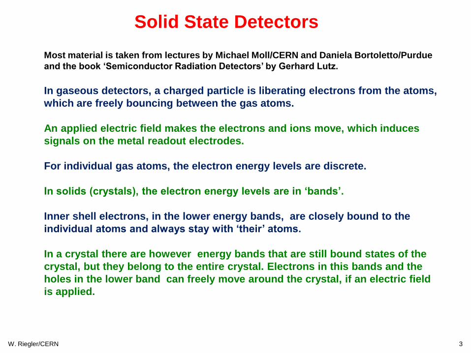
Most material is taken from lectures by Michael Moll/CERN and Daniela Bortoletto/Purdue
and the book ‘Semiconductor Radiation Detectors’ by Gerhard Lutz.
In gaseous detectors, a charged particle is liberating electrons from the atoms,
which are freely bouncing between the gas atoms.
An applied electric field makes the electrons and ions move, which induces
signals on the metal readout electrodes.
For individual gas atoms, the electron energy levels are discrete.
In solids (crystals), the electron energy levels are in ‘bands’.
Inner shell electrons, in the lower energy bands, are closely bound to the
individual atoms and always stay with ‘their’ atoms.
In a crystal there are however energy bands that are still bound states of the
crystal, but they belong to the entire crystal. Electrons in this bands and the
holes in the lower band can freely move around the crystal, if an electric field
is applied.
W. Riegler/CERN 3
Solid State Detectors

W. Riegler/CERN 4
Solid State Detectors
Free Electron Energy
Unfilled Bands
Conduction Band
Band Gap
Valance Band

In case the conduction band is filled the crystal is a conductor.
In case the conduction band is empty and ‘far away’ from the valence band, the
crystal is an insulator.
In case the conduction band is empty but the distance to the valence band is
small, the crystal is a semiconductor.
The energy gap between the last filled band – the valence band – and the
conduction band is called band gap Eg.
The band gap of Diamond/Silicon/Germanium is 5.5, 1.12, 0.66 eV.
The average energy to produce an electron/hole pair for
Diamond/Silicon/Germanium is 13, 3.6, 2.9eV.
In case an electron in the valence band gains energy by some process, it can be
excited into the conduction band and a hole in the valence band is left behind.
Such a process can be the passage of a charged particle, but also thermal
excitation probability is proportional Exp(-Eg/kT).
The number of electrons in the conduction band is therefore increasing with
temperature i.e. the conductivity of a semiconductor increases with temperature.
W. Riegler/CERN 5
Solid State Detectors

W. Riegler/CERN 6
Solid State Detectors

It is possible to treat electrons in the conduction band and holes in the valence band
similar to free particles, but with and effective mass different from elementary
electrons not embedded in the lattice.
This mass is furthermore dependent on other parameters such as the direction of
movement with respect to the crystal axis. All this follows from the QM treatment of
the crystal.
If we want to use a semiconductor as a detector for charged particles, the number of
charge carriers in the conduction band due to thermal excitation must be smaller than
the number of charge carriers in the conduction band produced by the passage of a
charged particle.
W. Riegler/CERN 7
Solid State Detectors
Diamond (Eg=5.5eV) can be used for particle
detection at room temperature, Silicon (Eg=1.12
eV) and Germanium (Eg=0.66eV) must be
cooled, or the free charge carriers must be
eliminated by other tricks doping see later.

The average energy to produce an electron/hole pair for Diamond/Silicon/Germanium
is 13, 3.6, 2.9eV.
Comparing to gas detectors, the density of a solid is about a factor 1000 larger than
that of a gas and the energy to produce and electron/hole pair e.g. for Si is a factor 7
smaller than the energy to produce an electron-ion pair in Argon.
The number of primary charges in a Si detector is therefore about 104 times larger
than the one in gas while gas detectors need internal charge amplification, solid
state detectors don’t need internal amplification.
While in gaseous detectors, the velocity of electrons and ions differs by a factor 1000,
the velocity of electrons and holes in many semiconductor detectors is quite similar.
W. Riegler/CERN 8
Solid State Detectors
Diamond A solid state
ionization chamber

Diamond Detector
W. Riegler/CERN 9
Velocity:
μe=1800 cm2/Vs, μh=1600 cm2/Vs
Velocity = μE, 10kV/cm v=180 μm/ns Very fast signals of only a few ns length !
Typical thickness – a few 100μm.
<1000 charge carriers/cm3 at room temperature due to large band gap.
I1
I2
q,vh-q, ve
zZ=D
Z=0
Z=z0E
I1(t)
T=2-3ns
A single e/h par produced in the center

Diamond Detector
W. Riegler/CERN 10
I1
I2
q,vh-q, ve
Z=D
Z=0
Z=z0E
I1(t)
T=2-3ns
I1(t)
T=2-3ns
However, charges are
trapped along the track, only
about 50% of produced
primary charge is induced

Silicon Detector
W. Riegler/CERN 11
Velocity:
μe=1450 cm2/Vs, μh=505 cm2/Vs, 3.63eV per e-h
pair.
~11000 e/h pairs in 100μm of silicon.
However: Free charge carriers in Si:
T=300 K: n/h = 1.45 x 10¹⁰ / cm3 but only 33000e-
/h in 300m produced by a high energy particle.
Why can we use Si as a solid state detector ???

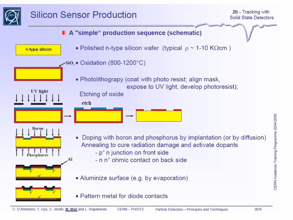
doping
p n
Doping of Silicon
W. Riegler/CERN 12
In a silicon crystal at a
given temperature the
number of electrons in
the conduction band is
equal to the number of
holes in the valence
band.
Doping Silicon with
Arsen (+5) it becomes
and n-type conductor
(more electrons than
holes).
Doping Silicon with
Boron (+3) it becomes a
p-type conductor (more
holes than electrons).
Bringing p and n in
contact makes a diode.
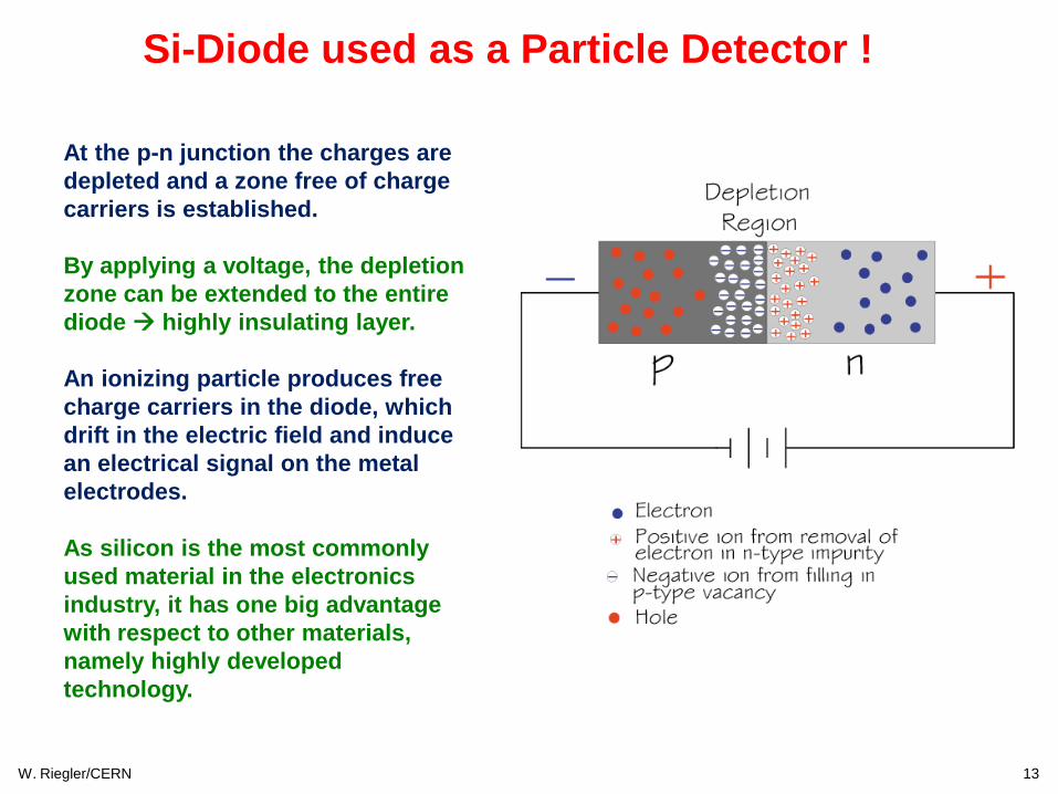
At the p-n junction the charges are
depleted and a zone free of charge
carriers is established.
By applying a voltage, the depletion
zone can be extended to the entire
diode highly insulating layer.
An ionizing particle produces free
charge carriers in the diode, which
drift in the electric field and induce
an electrical signal on the metal
electrodes.
As silicon is the most commonly
used material in the electronics
industry, it has one big advantage
with respect to other materials,
namely highly developed
technology.
W. Riegler/CERN 13
Si-Diode used as a Particle Detector !

Zone without free
charge carriers
positively charged.
Sensitive Detector
Volume.
W. Riegler/CERN 14
Under-Depleted Silicon Detector
np
++
+
++
+
+
++
++
+ +
++
+
++ +
+
++----
-- +-
Zone with free
electrons.
Conductive.
Insensitive to
particles.
Ele
ctr
ic F
ield
Zone without free charge carriers
positively charged.
Sensitive Detector Volume.
W. Riegler/CERN 15
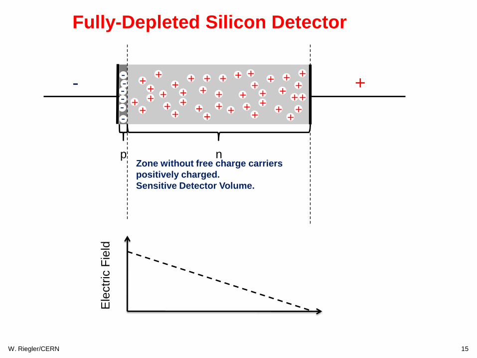
Fully-Depleted Silicon Detector
np
++
+
++
+
+
++
++
+ +
++
+
++ +
+
++----
-- +-
Ele
ctr
ic F
ield
++
+
++
+
++
+
+
+
+
+
++
+
++
Zone without free charge
carriers positively charged.
Sensitive Detector Volume.
W. Riegler/CERN 16
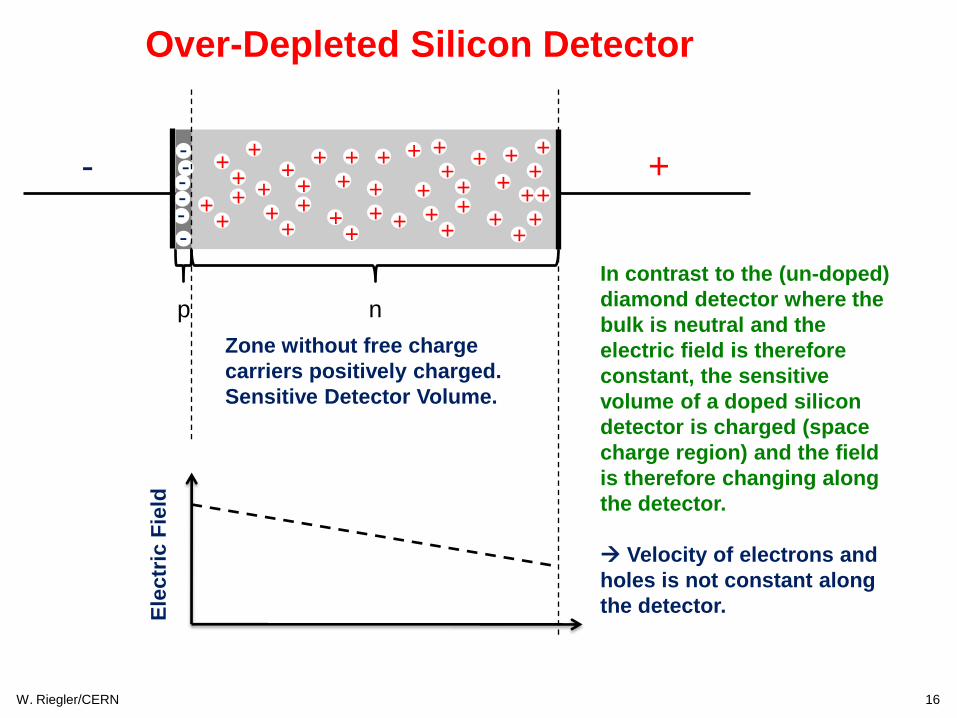
Over-Depleted Silicon Detector
np
++
+
++
+
+
++
++
+ +
++
+
++ +
+
++----
-- +-
Ele
ctr
ic F
ield
++
+
++
+
++
+
+
+
+
+
++
+
++
In contrast to the (un-doped)
diamond detector where the
bulk is neutral and the
electric field is therefore
constant, the sensitive
volume of a doped silicon
detector is charged (space
charge region) and the field
is therefore changing along
the detector.
Velocity of electrons and
holes is not constant along
the detector.

W. Riegler/CERN 17
Depletion Voltage
np
++
+
++
+
+
++
++
+ +
++
+
++ +
+
++----
-- +-
The capacitance of the detector decreases as the depletion zone increases.
Full depletion

W. Riegler/CERN 18
W. Riegler/CERN 19
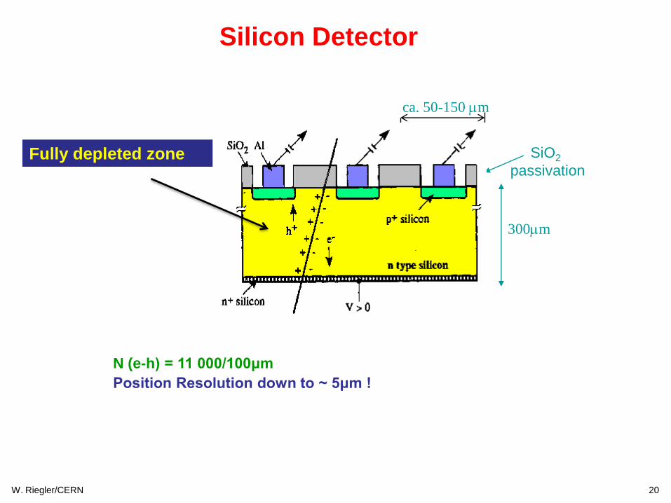
300m
SiO2
passivation
readout capacitances
ca. 50-150 m
Silicon Detector
W. Riegler/CERN 20
Fully depleted zone
N (e-h) = 11 000/100μm
Position Resolution down to ~ 5μm !

W. Riegler/CERN 21
p+
n-
n+
-V
d
xh xehole
electron
x0x
E
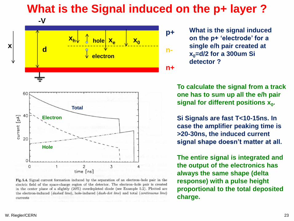
What is the Signal induced on the p+ layer ?
What is the signal induced
on the p+ ‘electrode’ for a
single e/h pair created at
x0=d/2 for a 300um Si
detector ?
W. Riegler/CERN 22
p+
n-
n+
-V
d
xh xehole
electron
x0x
E
What is the Signal induced on the p+ layer ?
W. Riegler/CERN 23
p+
n-
n+
-V
d
xh xehole
electron
x0x
What is the Signal induced on the p+ layer ?
What is the signal induced
on the p+ ‘electrode’ for a
single e/h pair created at
x0=d/2 for a 300um Si
detector ?
Electron
Hole
Total
To calculate the signal from a track
one has to sum up all the e/h pair
signal for different positions x0.
Si Signals are fast T<10-15ns. In
case the amplifier peaking time is
>20-30ns, the induced current
signal shape doesn’t matter at all.
The entire signal is integrated and
the output of the electronics has
always the same shape (delta
response) with a pulse height
proportional to the total deposited
charge.

Biasing, AC coupling
W. Riegler/CERN 25
W. Riegler/CERN 26
W. Riegler/CERN 27

W. Riegler/CERN 28
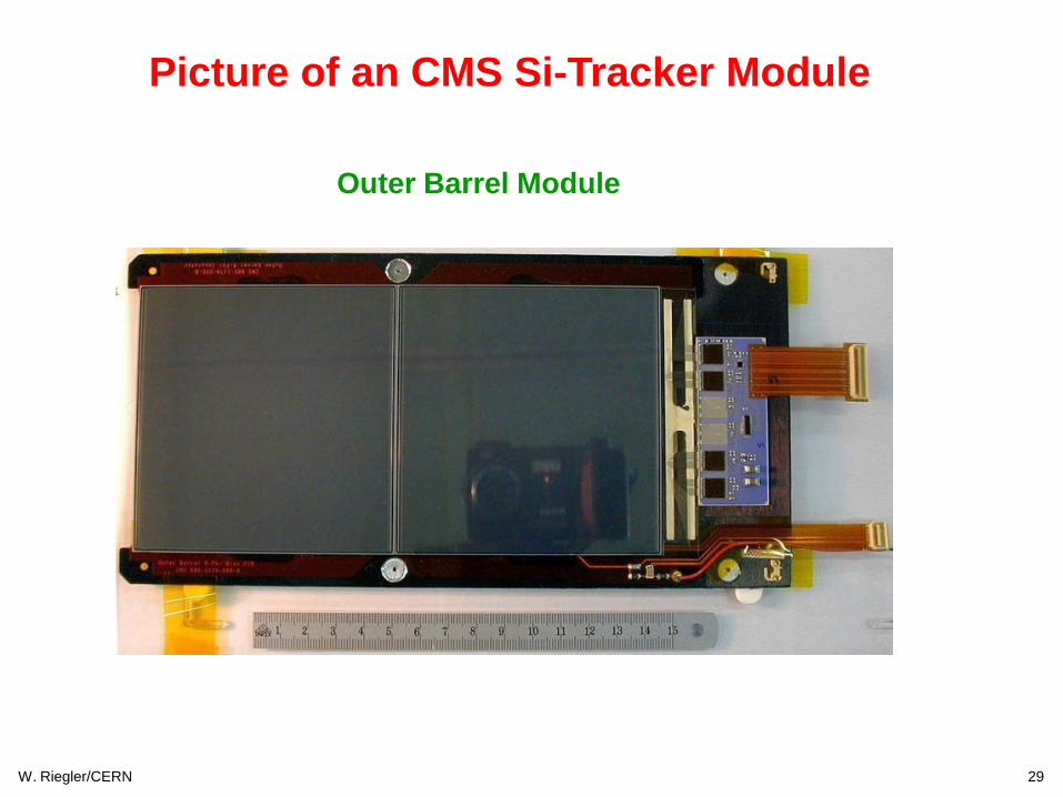
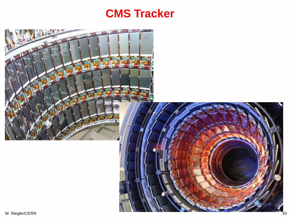
Outer Barrel Module
Picture of an CMS Si-Tracker Module
W. Riegler/CERN 29
W. Riegler/CERN 30
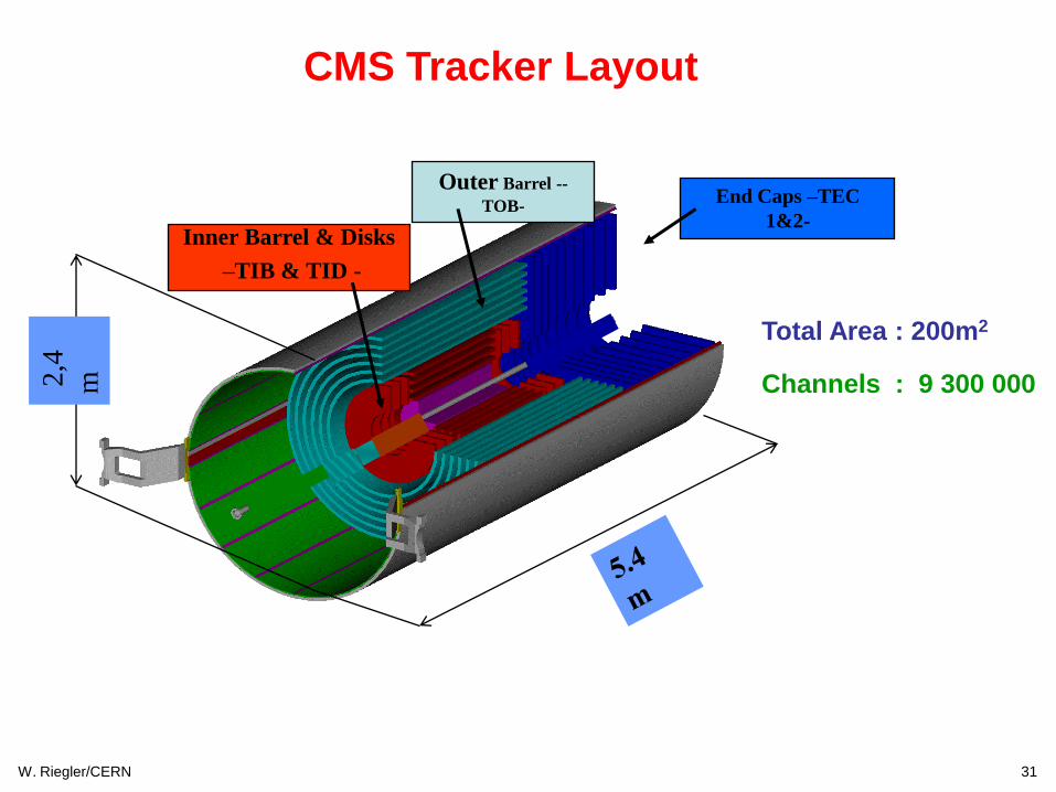
CMS Tracker Layout
Outer Barrel --
TOB-
Inner Barrel & Disks
–TIB & TID -
End Caps –TEC
1&2-
2,4
m
Total Area : 200m2
Channels : 9 300 000
W. Riegler/CERN 31
W. Riegler/CERN 32
W. Riegler/CERN 33
CMS Tracker

ionizing particle
Collection
drift cathodespull-up
cathode
bias HV divider
Silicon Drift Detector (like gas TPC !)
W. Riegler/CERN 34
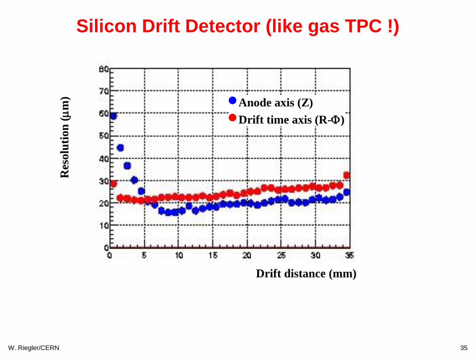
Drift distance (mm)
Res
olu
tion
(
m) Anode axis (Z)
Drift time axis (R-F)
W. Riegler/CERN 35
Silicon Drift Detector (like gas TPC !)

Pixel-Detectors
W. Riegler/CERN 36
Problem:
2-dimensional readout of strip detectors results in ‘Ghost Tracks’ at
high particle multiplicities i.e. many particles at the same time.
Solution:
Si detectors with 2 dimensional ‘chessboard’ readout. Typical size 50
x 200 μm.
Problem:
Coupling of readout electronics to the detector.
Solution:
Bump bonding.

Bump Bonding of each Pixel Sensor to the
Readout Electronics
W. Riegler/CERN 37
ATLAS: 1.4x108 pixels
W. Riegler/CERN 38
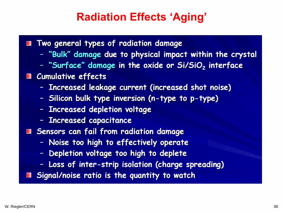
Radiation Effects ‘Aging’

W. Riegler/CERN 39
Radiation Effects ‘Aging’
Increase in leakage current
Increase in depletion voltage
Decrease in charge collection efficiency due to underdepletion
and charge trapping.

W. Riegler/CERN 40
Radiation Effects ‘Aging’
Type inversion ! An n-tyle Si detector becomes a p-type Si detector !
VCI 2004 summary 41
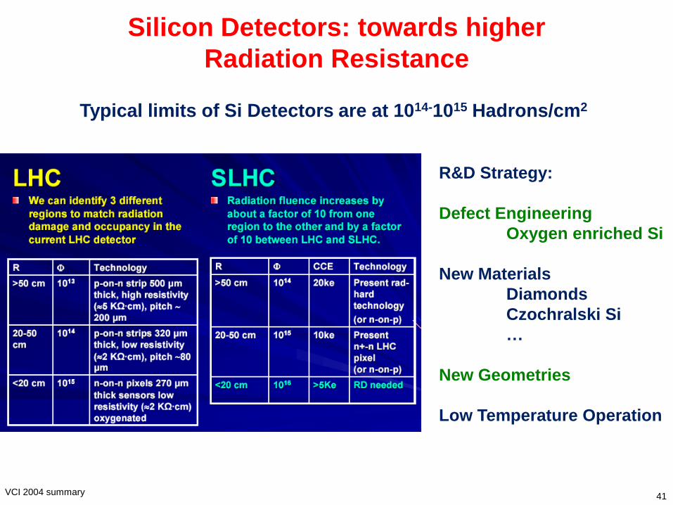
Silicon Detectors: towards higher
Radiation Resistance
R&D Strategy:
Defect Engineering
Oxygen enriched Si
New Materials
Diamonds
Czochralski Si
…
New Geometries
Low Temperature Operation
Typical limits of Si Detectors are at 1014-1015 Hadrons/cm2

VCI 2004 summary 42
New Materials: Polycrystalline Diamond
VCI 2004 summary 43
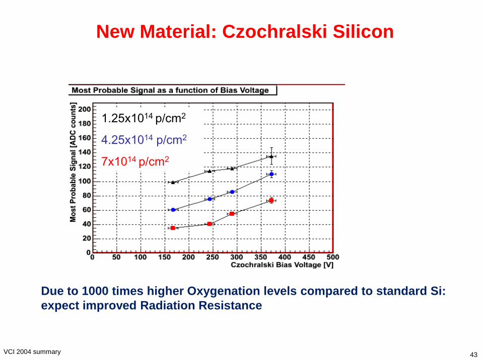
New Material: Czochralski Silicon
1.25x10¹⁴ p/cm2
4.25x10¹⁴ p/cm2
7x10¹⁴ p/cm2
Due to 1000 times higher Oxygenation levels compared to standard Si:
expect improved Radiation Resistance
VCI 2004 summary 44
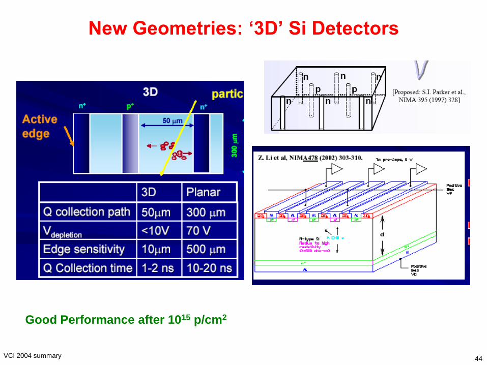
New Geometries: ‘3D’ Si Detectors
Good Performance after 1015 p/cm2
VCI 2004 summary 45
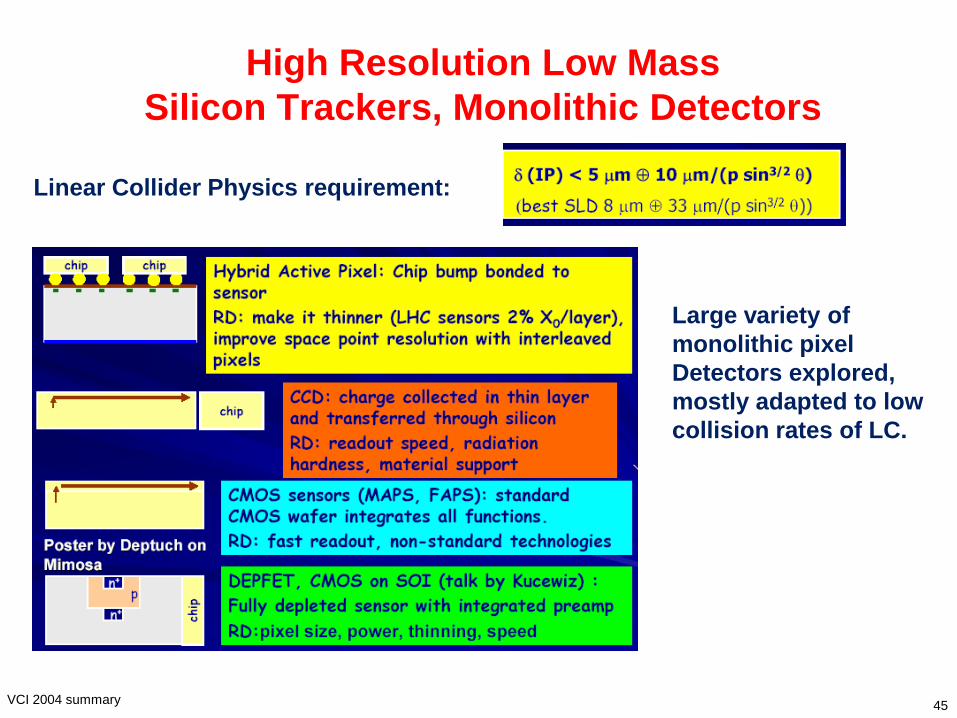
High Resolution Low Mass
Silicon Trackers, Monolithic Detectors
Linear Collider Physics requirement:
Large variety of
monolithic pixel
Detectors explored,
mostly adapted to low
collision rates of LC.

W. Riegler/CERN 46
Summary on Solid State Detectors
Solid state detectors provide very high precision tracking in particle
physics experiments (down to 5um) for vertex measurement but also
for momentum spectroscopy over large areas (CMS).
Technology is improving rapidly due to rapis Silicon development for
electronics industry.
Typical number where detectors start to strongly degrade are 1014-1015
hadron/cm2.
Diamond, engineered Silicon and novel geometries provide higher
radiation resistance.
Clearly, monolithic solid state detectors are the ultimate goal. Current
developments along these lines are useful for low rate applications. ar

W. Riegler/CERN 47
Thanks you your attention !
See you on Monday at 11:00 for calorimetry
or some time in the future around a particle detector.