28. particle detectors - particle data grouppdg.lbl.gov/2007/reviews/pardetrpp.pdf · 28. particle...
TRANSCRIPT

28. Particle detectors 1
28. PARTICLE DETECTORS
Revised 2007 (see the various sections for authors).
28.1. Summary of detector spatial resolution, temporal resolution,and deadtime
In this section we give various parameters for common detector components. Thequoted numbers are usually based on typical devices, and should be regarded only asrough approximations for new designs. More detailed discussions of detectors and theirunderlying physics can be found in books by Ferbel [1], Grupen [2], Kleinknecht [3],Knoll [4], and Green [5]. In Table 28.1 are given typical resolutions and deadtimes ofcommon detectors.
Table 28.1: Typical resolutions and deadtimes of common detectors. RevisedSeptember 2003 by R. Kadel (LBNL).
Resolution DeadDetector Type Accuracy (rms) Time Time
Bubble chamber 10–150 µm 1 ms 50 msa
Streamer chamber 300 µm 2 µs 100 msProportional chamber 50–300 µmb,c,d 2 ns 200 nsDrift chamber 50–300 µm 2 nse 100 nsScintillator — 100 ps/nf 10 nsEmulsion 1 µm — —Liquid Argon Drift [Ref. 6] ∼175–450 µm ∼ 200 ns ∼ 2 µsGas Micro Strip [Ref. 7] 30–40 µm < 10 ns —Resistive Plate chamber [Ref. 8] 10 µm 1–2 ns —
Silicon strip pitch/(3 to 7)g h h
Silicon pixel 2 µmi h h
a Multiple pulsing time.b 300 µm is for 1 mm pitch.c Delay line cathode readout can give ±150 µm parallel to anode wire.d wirespacing/
√12.
e For two chambers.f n = index of refraction.g The highest resolution (“7”) is obtained for small-pitch detectors ( 25 µm) with
pulse-height-weighted center finding.h Limited by the readout electronics [9]. (Time resolution of ≤ 25 ns is planned for
the ATLAS SCT.)i Analog readout of 34 µm pitch, monolithic pixel detectors.
CITATION: W.-M. Yao et al., Journal of Physics G 33, 1 (2006)
available on the PDG WWW pages (URL: http://pdg.lbl.gov/) November 29, 2007 14:50

2 28. Particle detectors
28.2. Photon detectors
Updated August 2007 by D. Chakraborty (Northern Illinois U) and T. Sumiyoshi (TokyoMetro U).
Most detectors in high-energy, nuclear, and astrophysics rely on the detection ofphotons in or near the visible range, 100 nm λ 1000 nm, or E ≈ a few eV. Thisrange covers scintillation and Cherenkov radiation as well as the light detected in manyastronomical observations.
Generally, photodetection involves generating a detectable electrical signal proportionalto the (usually very small) number of incident photons. The process involves three distinctsteps:1. Generation of a primary photoelectron or electron-hole (e-h) pair by an incident
photon by the photoelectric or photoconductive effect,2. Amplification of the p.e. signal to detectable levels by one or more multiplicative
bombardment steps and/or an avalanche process (usually), and,3. Collection of the secondary electrons to form the electrical signal.
The important characteristics of a photodetector include the following in statisticalaverages:1. Quantum efficiency (QE or εQ): the number of primary photoelectrons generated per
incident photon (0 ≤ εQ ≤ 1; in silicon more than one e-h pair per incident photoncan be generated for λ <∼ 165 nm),
2. Collection efficiency (CE or εC): the overall acceptance factor other than thegeneration of photoelectrons (0 ≤ εC ≤ 1),
3. Gain (G): the number of electrons collected for each photoelectron generated,4. Dark current or dark noise: the electrical signal when there is no photon,5. Energy resolution: electronic noise (ENC or Ne) and statistical fluctuations in the
amplification process compound the Poisson distribution of nγ photons from a givensource:
σ(E)〈E〉 =
√fN
nγεQεC+
(Ne
GnγεQεC
)2, (28.1)
where fN , or the excess noise factor (ENF), is the contribution to the energydistribution variance due to amplification statistics [10],
6. Dynamic range: the maximum signal available from the detector (this is usuallyexpressed in units of the response to noise-equivalent power, or NEP, which is theoptical input power that produces a signal-to-noise ratio of 1),
7. Time dependence of the response: this includes the transit time, which is the timebetween the arrival of the photon and the electrical pulse, and the transit time spread,which contributes to the pulse rise time and width, and
8. Rate capability: inversely proportional to the time needed, after the arrival of onephoton, to get ready to receive the next.The QE is a strong function of the photon wavelength (λ), and is usually quoted at
maximum, together with a range of λ where the QE is comparable to its maximum.
November 29, 2007 14:50

28. Particle detectors 3
Spatial uniformity and linearity with respect to the number of photons are highlydesirable in a photodetector’s response.
Optimization of these factors involves many trade-offs and vary widely betweenapplications. For example, while a large gain is desirable, attempts to increase the gainfor a given device also increases the ENF and after-pulsing (“echos” of the main pulse).In solid-state devices, a higher QE often requires a compromise in the timing properties.In other types, coverage of large areas by focusing increases the transit time spread.
Other important considerations also are highly application-specific. These include thephoton flux and wavelength range, the total area to be covered and the efficiency required,the volume available to accommodate the detectors, characteristics of the environmentsuch as chemical composition, temperature, magnetic field, ambient background, as wellambient radiation of different types and, mode of operation (continuous or triggered),bias (high-voltage) requirements, power consumption, calibration needs, aging, cost, andso on. Several technologies employing different phenomena for the three steps describedabove, and many variants within each, offer a wide range of solutions to choose from. Thesalient features of the main technologies and the common variants are described below.Some key characteristics are summarized in Table 28.2.
Table 28.2: Representative characteristics of some photodetectors commonlyused in particle physics. The time resolution of the devices listed here vary in the10–2000 ps range.
Type λ εQ εC Gain Risetime Area 1-p.e noise HV Price(nm) (ns) (mm2) (Hz) (V) (USD)
PMT∗ 115–1100 0.15–0.25 103–107 0.7–10 102–105 10–104 500–3000 100–5000MCP∗ 100–650 0.01–0.10 103–107 0.15–0.3 102–104 0.1–200 500–3500 10–6000HPD∗ 115–850 0.1–0.3 103–104 7 102–105 10–103 ∼2 × 10⁴ ∼600GPM∗ 115–500 0.15–0.3 103–106 O(0.1) O(10) 10–103 300–2000 O(10)APD 300–1700 ∼0.7 10–108 O(1) 10–103 1–103 400–1400 O(100)PPD 400–550 0.15–0.3 105–106 ∼ 1 1–10 O(106) 30–60 O(10)VLPC 500–600 ∼0.9 ∼5 × 10⁴ ∼ 10 1 O(104) ∼7 ∼1
∗These devices often come in multi-anode configurations. In such cases, area, noise, andprice are to be considered on a “per readout-channel” basis.
28.2.1. Vacuum photodetectors : Vacuum photodetectors can be broadly subdividedinto three types: photomultiplier tubes, microchannel plates, and hybrid photodetectors.
28.2.1.1. Photomultiplier tubes: A versatile class of photon detectors, vacuumphotomultiplier tubes (PMT) has been employed by a vast majority of all particle physicsexperiments to date [10]. Both “transmission-” and “reflection-type” PMT’s are widelyused. In the former, the photocathode material is deposited on the inside of a transparentwindow through which the photons enter, while in the latter, the photocathode material
November 29, 2007 14:50

4 28. Particle detectors
rests on a separate surface that the incident photons strike. The cathode material hasa low work function, chosen for the wavelength band of interest. When a photon hitsthe cathode and liberates an electron (the photoelectric effect), the latter is acceleratedand guided by electric fields to impinge on a secondary-emission electrode, or dynode,which then emits a few (∼ 5) secondary electrons. The multiplication process is repeatedtypically 10 times in series to generate a sufficient number of electrons, which are collectedat the anode for delivery to the external circuit. The total gain of a PMT depends onthe applied high voltage V as G = AV kn, where k ≈ 0.7–0.8 (depending on the dynodematerial), n is the number of dynodes in the chain, and A a constant (which also dependson n). Typically, G is in the range of 105–106. Pulse risetimes are usually in the fewnanosecond range. With e.g. two-level discrimination the effective time resolution can bemuch better.
A large variety of PMT’s, including many just recently developed, covers a wide spanof wavelength ranges from infrared (IR) to extreme ultraviolet (XUV) [11]. They arecategorized by the window materials, photocathode materials, dynode structures, anodeconfigurations, etc. Common window materials are borosilicate glass for IR to near-UV,fused quartz and sapphire (Al2O3) for UV, and MgF2 or LiF for XUV. The choiceof photocathode materials include a variety of mostly Cs- and/or Sb-based compoundssuch as CsI, CsTe, bi-alkali (SbRbCs, SbKCs), multi-alkali (SbNa2KCs), GaAs(Cs),GaAsP, etc. Sensitive wavelengths and peak quantum efficiencies for these materials aresummarized in Table 28.3. Typical dynode structures used in PMT’s are circular cage,line focusing, box and grid, venetian blind, and fine mesh. In some cases, limited spatialresolution can be obtained by using a mosaic of multiple anodes.
PMT’s are vulnerable to magnetic fields—sometimes even the geomagnetic field causeslarge orientation-dependent gain changes. A high-permeability metal shield is oftennecessary. However, proximity-focused PMT’s, e.g. the fine-mesh types, can be used evenin a high magnetic field (≥ 1 T) if the electron drift direction is parallel to the field.
28.2.1.2. Microchannel plates: A typical Microchannel plate (MCP) photodetectorconsists of one or more ∼2 mm thick glass plates with densely packed O(10 µm)-diametercylindrical holes, or “channels”, sitting between the transmission-type photocathodeand anode planes, separated by O(1 mm) gaps. Instead of discrete dynodes, the innersurface of each cylindrical tube serves as a continuous dynode for the entire cascadeof multiplicative bombardments initiated by a photoelectron. Gain fluctuations can beminimized by operating in a saturation mode, whence each channel is only capable of abinary output, but the sum of all channel outputs remains proportional to the number ofphotons received so long as the photon flux is low enough to ensure that the probabilityof a single channel receiving more than one photon during a single time gate is negligible.MCP’s are thin, offer good spatial resolution, have excellent time resolution (∼20 ps), andcan tolerate random magnetic fields up to 0.1 T and axial fields up to ∼ 1 T. However,they suffer from relatively long recovery time per channel and short lifetime. MCP’s arewidely employed as image-intensifiers, although not so much in HEP or astrophysics.
November 29, 2007 14:50

28. Particle detectors 5
28.2.1.3. Hybrid photon detectors: Hybrid photon detectors (HPD) combine thesensitivity of a vacuum PMT with the excellent spatial and energy resolutions of a Sisensor [19]. A single photoelectron ejected from the photocathode is accelerated througha potential difference of ∼20 kV before it impinges on the silicon sensor/anode. The gainnearly equals the maximum number of e-h pairs that could be created from the entirekinetic energy of the accelerated electron: G ≈ eV/w, where e is the electronic charge,V is the applied potential difference, and w ≈ 3.7 eV is the mean energy required tocreate an e-h pair in Si at room temperature. Since the gain is achieved in a single step,one might expect to have the excellent resolution of a simple Poisson statistic with largemean, but in fact it is even better, thanks to the Fano effect discussed in Sec. 28.8.
Low-noise electronics must be used to read out HPD’s if one intends to take advantageof the low fluctuations in gain, e.g. when counting small numbers of photons. HPD’s canhave the same εQ εC and window geometries as PMT’s and can be segmented down to∼50 µm. However, they require rather high biases and will not function in a magneticfield. The exception is proximity-focused devices (⇒ no (de)magnification) in an axialfield. With time resolutions of ∼10 ps and superior rate capabiility, proximity-focusedHPD’s can be an alternative to MCP’s. Current applications of HPD’s include theCMS hadronic calorimeter and the RICH detector in LHCb. Large-size HPD’s withsophisticated focusing may be suitable for future water Cherenkov experiments.
Hybrid APD’s (HAPD’s) add an avalanche multiplication step following the electronbombardment to boost the gain by a factor of ∼50. This affords a higher gain and/orlower electrical bias, but also degrades the signal definition.
Table 28.3: Properties of photocathode and window materials commonly used invacuum photodetectors [11].
Photocathode λ Window Peak εQ (λ/nm)material (nm) material
CsI 115–200 MgF2 0.15 (135)CsTe 115–240 MgF2 0.18 (210)Bi-alkali 300–650 Borosilicate 0.27 (390)
160-650 Quartz 0.27 (390)Multi-alkali 300–850 Borosilicate 0.20 (360)
160-850 Quartz 0.23 (280)GaAs(Cs)∗ 160–930 Quartz 0.23 (280)GaAsP(Cs) 300-750 Borosilicate 0.42 (560)
∗Reflection type photocathode is used.
November 29, 2007 14:50

6 28. Particle detectors
28.2.2. Gaseous photon detectors : In gaseous photomultipliers (GPM) aphotoelectron in a suitable gas mixture initiates an avalanche in a high-field region,producing a large number of secondary impact-ionization electrons. In principle thecharge multiplication and collection processes are identical to those employed in gaseoustracking detectors such as multiwire proportional chambers, micromesh gaseous detectors(Micromegas), or gas electron multipliers (GEM). These are discussed in Sections 28.7and 28.7.
The devices can be divided into two types depending on the photocathode material.One type uses solid photocathode materials much in the same way as PMT’s. Since it isresistant to gas mixtures typically used in tracking chambers, CsI is a common choice.In the other type, photoionization occurs on suitable molecules vaporized and mixed inthe drift volume. Most gases have photoionization work functions in excess of 10 eV,which would limit their sensitivity to wavelengths far too short. However, vapors ofTMAE (tetrakis dimethyl-amine ethylene) or TEA (tri-ethyl-amine), which have smallerwork functions (5.3 eV for TMAE and 7.5 eV for TEA), are suited for XUV photondetection [12]. Since devices like GEM’s offer sub-mm spatial resolution, GPM’s areoften used as position-sensitive photon detectors. They can be made into flat panelsto cover large areas (O(1 m2)), can operate in high magnetic fields, and are relativelyinexpensive. Many of the ring imaging Cherenkov (RICH) detectors to date have usedGPM’s for the detection of Cherenkov light [13]. Special care must be taken to suppressthe photon-feedback process in GPM’s. It is also important to maintain high purity ofthe gas as minute traces of O2 can significantly degrade the detection efficiency.
28.2.3. Solid-state photon detectors : In a phase of rapid development, solid-statephotodetectors are competing with vacuum- or gas-based devices for many existingapplications and making way for a multitude of new ones. Compared to traditionalvacuum- and gaseous photodetectors, solid-state devices are more compact, lightweight,rugged, tolerant to magnetic fields, and often cheaper. They also allow fine pixelization,are easy to integrate into large systems, and can operate at low electric potentials, whilematching or exceeding most performance criteria. They are particularly well suited fordetection of γ- and X-rays. Except for applications where coverage of very large areasor dynamic range is required, solid-state detectors are proving to be the better choice.Some hybrid devices attempt to combine the best features of different technologies whileapplications of nanotechnology are opening up exciting new possibilities.
Silicon photodiodes (PD) are widely used in high-energy physics as particle detectorsand in a great number of applications (including solar cells!) as light detectors. Thestructure is discussed in some detail in Sec. 28.8. In its simplest form, the PD is areverse-biased p-n junction. Photons with energies above the indirect bandgap energy(wavelengths shorter than about 1050 nm, depending on the temperature) can create e-hpairs (the photoconductive effect), which are collected on the p and n sides, respectively.Often, as in the PD’s used for crystal scintillator readout in CLEO, L3, Belle,BaBar,and GLAST, intrinsic silicon is doped to create a p-i-n structure. The reverse biasincreases the thickness of the depleted region; in the case of these particular detectors,to full depletion at a depth of about 100 µm. Increasing the depletion depth decreasesthe capacitance (and hence electronic noise) and extends the red response. Quantum
November 29, 2007 14:50

28. Particle detectors 7
efficiency can exceed 90%, but falls toward the red because of the increasing absorptionlength of light in silicon. The absorption length reaches 100 µm at 985 nm. However,since G = 1, amplification is necessary. Optimal low-noise amplifiers are slow, but, evenso, noise limits the minimum detectable signal in room-temperature devices to severalhundred photons.
Very large arrays containing O(107) of O(10 µm2)-sized photodioides pixelizing aplane are widely used to photograph all sorts of things from everyday subjects at visiblewavelengths to crystal structures with X-rays and astronomical objects from infrared toUV. To limit the number of readout channels, these are made into charge-coupled devices(CCD), where pixel-to-pixel signal transfer takes place over thousands of synchronouscycles with sequential output through shift registers [14]. Thus, high spatial resolutionis achieved at the expense of speed and timing precision. Custom-made CCD’s havevirtually replaced photographic plates and other imagers for astronomy and in spacecraft.Typical QE’s exceed 90% over much of the visible spectrum, and “thick” CCD’s haveuseful QE up to λ = 1 µm. Active Pixel Sensor (APS) arrays with a preamplifier oneach pixel and CMOS processing afford higher speeds, but are challenged at longerwavelengths. Much R&D is underway to overcome the limitations of both CCD andCMOS imagers.
In avalanche photodiodes (APD), an exponential cascade of impact ionizations initiatedby the initial photogenerated e-h pair under a large reverse-bias voltage leads to anavalanche breakdown [15]. As a result, detectable electrical response can be obtainedfrom low-intensity optical signals down to single photons. Excellent junction uniformity iscritical, and a guard ring is generally used as a protection against edge breakdown. Well-designed APD’s, such as those used in CMS’ crystal-based electromagnetic calorimeter,have achieved εQ εC ≈ 0.7 with sub-ns response time. The sensitive wavelength windowand gain depend on the semiconductor used. The gain is typically 10–200 in linear andup to 108 in Geiger mode of operation. Stability and close monitoring of the operatingtemperature are important for linear-mode operation, and substantial cooling is oftennecessary. Position-sensitive APD’s use time information at multiple anodes to calculatethe hit position.
One of the most promising recent developments in the field is that of devices consistingof large arrays (O(103)) of tiny APD’s packed over a small area (O(1 mm2)) andoperated in a limited Geiger mode [16]. Among different names used for this classof photodetectors, “PPD” (for “Pixelized Photon Detector”) is most widely accepted(formerly “SiPM”). Although each cell only offers a binary output, linearity with respectto the number of photons is achieved by summing the cell outputs in the same way as witha MCP in saturation mode (see above). PPD’s are being adopted as the preferred solutionfor various purposes including medical imaging, e.g. positron emission tomography (PET).These compact, rugged, and economical devices allow auto-calibration through decentseparation of photoelectron peaks and offer gains of O(106) at a moderate bias voltage(∼50 V). However, the single-photoelectron noise of a PPD, being the logical “or” ofO(103) Geiger APD’s, is rather large: O(1 MHz/mm2) at room temperature. PPD’s areparticularly well-suited for applications where triggered pulses of several photons areexpected over a small area, e.g. fiber-guided scintillation light. Intense R&D is expeced
November 29, 2007 14:50

8 28. Particle detectors
to lower the noise level and improve radiation hardness, resulting in coverage of largerareas and wider applications. Attempts are being made to combine the fabrication of thesensors and the front-end electronics (ASIC) in the same process with the goal of makingPPD’s and other finely pixelized solid-state photodetectors extremely easy to use.
Of late, much R&D has been directed to p-i-n diode arrays based on thin polycrystallinediamond films formed by chemical vapor deposition (CVD) on a hot substrate (∼1000K) from a hydrocarbon-containing gas mixture under low pressure (∼100 mbar).These devices have maximum sensitivity in the extreme- to moderate-UV region [17].Many desirable characteristics, including high tolerance to radiation and temperaturefluctuations, low dark noise, blindness to most of the solar radiation spectrum, andrelatively low cost make them ideal for space-based UV/XUV astronomy, measurement ofsynchrotron radiation, and luminosity monitoring at (future) lepton collider(s).
Visible-light photon counters (VLPC) utilize the formation of an impurity band only50 meV below the conduction band in As-doped Si to generate strong (G ≈ 5 × 10⁴)yet sharp response to single photons with εQ ≈ 0.9 [18]. The smallness of the bandgap considerably reduces the gain dispersion. Only a very small bias (∼7 V) is needed,but high sensitivity to infrared photons requires cooling below 10 K. The dark noiseincreases sharply and exponentially with both temperature and bias. The Run 2 DØdetector uses 86000 VLPC’s to read the optical signal from its scintillating-fiber trackerand scintillator-strip preshower detectors.
28.3. Organic scintillators
Revised September 2007 by K.F. Johnson (FSU).
Organic scintillators are broadly classed into three types, crystalline, liquid, and plastic,all of which utilize the ionization produced by charged particles (see Sec. 27.2) of thisReview) to generate optical photons, usually in the blue to green wavelength regions [20].Plastic scintillators are by far the most widely used. Crystal organic scintillators arepractically unused in high-energy physics.
Densities range from 1.03 to 1.20 g cm−3. Typical photon yields are about 1 photonper 100 eV of energy deposit [21]. A one-cm-thick scintillator traversed by a minimum-ionizing particle will therefore yield ≈ 2×10⁴ photons. The resulting photoelectron signalwill depend on the collection and transport efficiency of the optical package and thequantum efficiency of the photodetector.
Plastic scintillators do not respond linearly to the ionization density. Very denseionization columns emit less light than expected on the basis of dE/dx for minimum-ionizing particles. A widely used semi-empirical model by Birks posits that recombinationand quenching effects between the excited molecules reduce the light yield [22]. Theseeffects are more pronounced the greater the density of the excited molecules. Birks’formula is
dL
dx= L0
dE/dx
1 + kB dE/dx,
where L is the luminescence, L0 is the luminescence at low specific ionization density,and kB is Birks’ constant, which must be determined for each scintillator by measurement.
November 29, 2007 14:50

28. Particle detectors 9
Decay times are in the ns range; rise times are much faster. The combination of highlight yield and fast response time allows the possibility of sub-ns timing resolution [23].The fraction of light emitted during the decay “tail” can depend on the exciting particle.This allows pulse shape discrimination as a technique to carry out particle identification.Because of the hydrogen content (carbon to hydrogen ratio ≈ 1) plastic scintillator issensitive to proton recoils from neutrons. Ease of fabrication into desired shapes andlow cost has made plastic scintillators a common detector component. Recently, plasticscintillators in the form of scintillating fibers have found widespread use in tracking andcalorimetry [24].
28.3.1. Scintillation mechanism :Scintillation: A charged particle traversing matter leaves behind it a wake of excitedmolecules. Certain types of molecules, however, will release a small fraction (≈ 3%)of this energy as optical photons. This process, scintillation, is especially marked inthose organic substances which contain aromatic rings, such as polystyrene (PS) andpolyvinyltoluene (PVT). Liquids which scintillate include toluene and xylene.
Fluorescence: In fluorescence, the initial excitation takes place via the absorption of aphoton, and de-excitation by emission of a longer wavelength photon. Fluors are usedas “waveshifters” to shift scintillation light to a more convenient wavelength. Occurringin complex molecules, the absorption and emission are spread out over a wide band ofphoton energies, and have some overlap, that is, there is some fraction of the emittedlight which can be re-absorbed [25]. This “self-absorption” is undesirable for detectorapplications because it causes a shortened attenuation length. The wavelength differencebetween the major absorption and emission peaks is called the Stokes’ shift. It is usuallythe case that the greater the Stokes’ shift, the smaller the self absorption—thus, a largeStokes’ shift is a desirable property for a fluor.
Ionization excitation of base plastic
Forster energy transfer
γ
γ
base plastic
primary fluor(~1% wt/wt )
secondary fluor(~0.05% wt/wt )
photodetector
emit UV, ~340 nm
absorb blue photon
absorb UV photon
emit blue, ~400 nm1 m
10−4m
10−8m
Figure 28.1: Cartoon of scintillation “ladder” depicting the operating mechanismof plastic scintillator. Approximate fluor concentrations and energy transferdistances for the separate sub-processes are shown.
November 29, 2007 14:50

10 28. Particle detectors
Scintillators: The plastic scintillators used in high-energy physics are binary or ternarysolutions of selected fluors in a plastic base containing aromatic rings. (See the appendixin Ref. 26 for a comprehensive list of components.) Virtually all plastic scintillatorscontain as a base either PVT or PS. PVT-based scintillator can be up to 50% brighter.
Ionization in the plastic base produces UV photons with short attenuation length(several mm). Longer attenuation lengths are obtained by dissolving a “primary” fluor inhigh concentration (1% by weight) into the base, which is selected to efficiently re-radiateabsorbed energy at wavelengths where the base is more transparent.
The primary fluor has a second important function. The decay time of the scintillatorbase material can be quite long—in pure polystyrene it is 16 ns, for example. Theaddition of the primary fluor in high concentration can shorten the decay time by anorder of magnitude and increase the total light yield. At the concentrations used (1%and greater), the average distance between a fluor molecule and an excited base unit isaround 100 A, much less than a wavelength of light. At these distances the predominantmode of energy transfer from base to fluor is not the radiation of a photon, but a resonantdipole-dipole interaction, first described by Foerster, which strongly couples the base andfluor [27]. The strong coupling sharply increases the speed and the light yield of theplastic scintillators.
Unfortunately, a fluor which fulfills other requirements is usually not completelyadequate with respect to emission wavelength or attenuation length, so it is necessaryto add yet another waveshifter (the “secondary” fluor), at fractional percent levels, andoccasionally a third (not shown in Fig. 28.1).
External wavelength shifters: Light emitted from a plastic scintillator may be absorbedin a (nonscintillating) base doped with a wave-shifting fluor. Such wavelength shifters arewidely used to aid light collection in complex geometries. The wavelength shifter mustbe insensitive to ionizing radiation and Cherenkov light. A typical wavelength shifteruses an acrylic base because of its good optical qualities, a single fluor to shift thelight emerging from the plastic scintillator to the blue-green, and contains ultra-violetabsorbing additives to deaden response to Cherenkov light.
28.3.2. Caveats and cautions : Plastic scintillators are reliable, robust, andconvenient. However, they possess quirks to which the experimenter must be alert.
Aging and Handling: Plastic scintillators are subject to aging which diminishes the lightyield. Exposure to solvent vapors, high temperatures, mechanical flexing, irradiation, orrough handling will aggravate the process. A particularly fragile region is the surfacewhich can “craze”—develop microcracks—which rapidly destroy the capability of plasticscintillators to transmit light by total internal reflection. Crazing is particularly likelywhere oils, solvents, or fingerprints have contacted the surface.
Attenuation length: The Stokes’ shift is not the only factor determining attenuationlength. Others are the concentration of fluors (the higher the concentration of a fluor, thegreater will be its self-absorption); the optical clarity and uniformity of the bulk material;
November 29, 2007 14:50

28. Particle detectors 11
the quality of the surface; and absorption by additives, such as stabilizers, which may bepresent.
Afterglow: Plastic scintillators have a long-lived luminescence which does not follow asimple exponential decay. Intensities at the 10−4 level of the initial fluorescence canpersist for hundreds of ns [20,28].
Atmospheric quenching: Plastic scintillators will decrease their light yield with increasingpartial pressure of oxygen. This can be a 10% effect in an artificial atmosphere [29]. Itis not excluded that other gases may have similar quenching effects.
Magnetic field: The light yield of plastic scintillators may be changed by a magnetic field.The effect is very nonlinear and apparently not all types of plastic scintillators are soaffected. Increases of ≈ 3% at 0.45 T have been reported [30]. Data are sketchy andmechanisms are not understood.
Radiation damage: Irradiation of plastic scintillators creates color centers which absorblight more strongly in the UV and blue than at longer wavelengths. This poorlyunderstood effect appears as a reduction both of light yield and attenuation length.Radiation damage depends not only on the integrated dose, but on the dose rate,atmosphere, and temperature, before, during and after irradiation, as well as thematerials properties of the base such as glass transition temperature, polymer chainlength, etc. Annealing also occurs, accelerated by the diffusion of atmospheric oxygenand elevated temperatures. The phenomena are complex, unpredictable, and not wellunderstood [31]. Since color centers are less intrusive at longer wavelengths, the mostreliable method of mitigating radiation damage is to shift emissions at every step to thelongest practical wavelengths, e.g., utilize fluors with large Stokes’ shifts (aka the “Betterred than dead” strategy).
28.3.3. Scintillating and wavelength-shifting fibers :The clad optical fiber is an incarnation of scintillator and wavelength shifter (WLS)
which is particularly useful [32]. Since the initial demonstration of the scintillating fiber(SCIFI) calorimeter [33], SCIFI techniques have become mainstream [34].
SCIFI calorimeters are fast, dense, radiation hard, and can have leadglass-likeresolution. SCIFI trackers can handle high rates and are radiation tolerant, but thelow photon yield at the end of a long fiber (see below) forces the use of sensitivephotodetectors. WLS scintillator readout of a calorimeter allows a very high level ofhermeticity since the solid angle blocked by the fiber on its way to the photodetector isvery small. The sensitive region of scintillating fibers can be controlled by splicing themonto clear (non-scintillating/non-WLS) fibers.
A typical configuration would be fibers with a core of polystyrene-based scintillator orWLS (index of refraction n = 1.59), surrounded by a cladding of PMMA (n = 1.49) a fewmicrons thick, or, for added light capture, with another cladding of fluorinated PMMAwith n = 1.42, for an overall diameter of 0.5 to 1 mm. The fiber is drawn from a bouleand great care is taken during production to ensure that the intersurface between thecore and the cladding has the highest possible uniformity and quality, so that the signal
November 29, 2007 14:50

12 28. Particle detectors
transmission via total internal reflection has a low loss. The fraction of generated lightwhich is transported down the optical pipe is denoted the capture fraction and is about6% for the single-clad fiber and 10% for the double-clad fiber.
The number of photons from the fiber available at the photodetector is always smallerthan desired, and increasing the light yield has proven difficult. A minimum-ionizingparticle traversing a high-quality 1 mm diameter fiber perpendicular to its axis willproduce fewer than 2000 photons, of which about 200 are captured. Attenuation mayeliminate 95% of these photons in a large collider tracker.
A scintillating or WLS fiber is often characterized by its “attenuation length,” overwhich the signal is attenuated to 1/e of its original value. Many factors determinethe attenuation length, including the importance of re-absorption of emitted photonsby the polymer base or dissolved fluors, the level of crystallinity of the base polymer,and the quality of the total internal reflection boundary. Attenuation lengths of severalmeters are obtained by high quality fibers. However, it should be understood that theattenuation length is not necessarily a measure of fiber quality. Among other things, itis not constant with distance from the excitation source and it is wavelength dependent.So-called “cladding light” causes some of the distance dependence [35], but not all. Thewavelength dependence is usually related to the higher re-absorption of shorter wavelengthphotons—once absorbed, re-emitted isotropically and lost with 90% probability—and tothe lower absorption of longer wavelengths by polystyrene. Experimenters should be awarethat measurements of attenuation length by a phototube with a bialkali photocathode,whose quantum efficiency drops below 10% at 480 nm, should not be naıvely comparedto measurements utilizing a silicon photodiode, whose quantum efficiency is still rising at600 nm.
28.4. Inorganic scintillators:
Revised September 2007 by R.-Y. Zhu (California Institute of Technology) andC.L. Woody (BNL).
Inorganic crystals form a class of scintillating materials with much higher densitiesthan organic plastic scintillators (typically ∼ 4–8 g/cm3) with a variety of differentproperties for use as scintillation detectors. Due to their high density and high effectiveatomic number, they can be used in applications where high stopping power or a highconversion efficiency for electrons or photons is required. These include total absorptionelectromagnetic calorimeters (see Sec. 28.10.1), which consist of a totally active absorber(as opposed to a sampling calorimeter), as well as serving as gamma ray detectors over awide range of energies. Many of these crystals also have very high light output, and cantherefore provide excellent energy resolution down to very low energies (∼ few hundredkeV).
Some crystals are intrinsic scintillators in which the luminescence is produced by apart of the crystal lattice itself. However, other crystals require the addition of a dopant,typically fluorescent ions such as thallium (Tl) or cerium (Ce) which is responsible forproducing the scintillation light. However, in both cases, the scintillation mechanism isthe same. Energy is deposited in the crystal by ionization, either directly by charged
November 29, 2007 14:50

28. Particle detectors 13
particles, or by the conversion of photons into electrons or positrons which subsequentlyproduce ionization. This energy is transferred to the luminescent centers which thenradiate scintillation photons. The efficiency η for the conversion of energy deposit in thecrystal to scintillation light can be expressed by the relation [36]
η = β · S · Q . (28.2)
where β is the efficiency of the energy conversion process, S is the efficiency of energytransfer to the luminescent center, and Q is the quantum efficiency of the luminescentcenter. The value of η ranges between 0.1 and ∼ 1 depending on the crystal, and isthe main factor in determining the intrinsic light output of the scintillator. In addition,the scintillation decay time is primarily determined by the energy transfer and emissionprocess. The decay time of the scintillator is mainly dominated by the decay time of theluminescent center. For example, in the case of thallium doped sodium iodide (NaI(Tl)),the value of η is ∼ 0.5, which results in a light output ∼ 40,000 photons per MeV ofenergy deposit. This high light output is largely due to the high quantum efficiency ofthe thallium ion (Q ∼ 1), but the decay time is rather slow (τ ∼ 250 ns).
Table 28.4 lists the basic properties of some commonly used inorganic crystalscintillators. NaI(Tl) is one of the most common and widely used scintillators, withan emission that is well matched to a bialkali photomultiplier tube, but it is highlyhygroscopic and difficult to work with, and has a rather low density. CsI(Tl) hashigh light yield, an emission that is well matched to solid state photodiodes, and ismechanically robust (high plasticity and resistance to cracking). However, it needs carefulsurface treatment and is slightly hygroscopic. Compared with CsI(Tl), pure CsI hasidentical mechanical properties, but faster emission at shorter wavelengths and lightoutput approximately an order of magnitude lower. BaF2 has a fast component witha sub-nanosecond decay time, and is the fastest known scintillator. However, it alsohas a slow component with a much longer decay time (∼ 630 ns). Bismuth gemanate(Bi4Ge3O12 or BGO) has a high density, and consequently a short radiation length X0
and Moliere radius RM . BGO’s emission is well-matched to the spectral sensitivity ofphotodiodes, and it is easy to handle and not hygroscopic. Lead tungstate (PbWO4 orPWO) has a very high density, with a very short X0 and RM , but its intrinsic light yieldis rather low. Cerium doped lutetium oxyorthosilicate (Lu2SiO5:Ce, or LSO:Ce) [37],cerium doped lutetium-yttrium oxyorthosilicate (Lu2(1−x)Y2xSiO5, LYSO:Ce) [38] andcerium doped gadolinium orthosilicate (Gd2SiO5:Ce, or GSO:Ce) [39] are dense crystalscintillators which have a high light yield and a fast decay time. Only properties ofLSO:Ce and GSO:Ce are listed in Table 28.4 since the properties of LYSO:Ce are similarto that of LSO:Ce except a little lower density than LSO:Ce depending on the yttriumfraction in LYSO:Ce [40].
Beside the crystals listed in Table 28.4, a number of new crystals are being developedthat may have potential applications in high energy or nuclear physics. Of particularinterest is the family of yttrium and lutetium perovskites, which include YAP (YAlO3:Ce)and LuAP (LuAlO3:Ce) and their mixed compositions. These have been shown to belinear over a large energy range [41], and have the potential for providing extremely good
November 29, 2007 14:50

14 28. Particle detectors
intrinsic energy resolution. In addition, other fluoride crystals such as CeF3 have beenshown to provide excellent energy resolution in calorimeter applications.
Table 28.4 gives the light output of other crystals relative to NaI(Tl) and theirdependence to the temperature variations measured for crystal samples of 1.5 X0 cubewith a Tyvek paper wrapping and a full end face coupled to a photodetector [42]. Thequantum efficiencies of the photodetector is taken out to facilitate a direct comparisonof crystal’s light output. However, the useful signal produced by a scintillator isusually quoted in terms of the number of photoelectrons per MeV produced by a givenphotodetector. The relationship between the number of photons/MeV produced andphotoelectrons/MeV detected involves the factors for the light collection efficiency L andthe quantum efficiency QE of the photodetector:
Np.e./MeV = L · QE · Nγ/MeV (28.3)
L includes the transmission of scintillation light within the crystal (i.e., the bulkattenuation length of the material), reflections and scattering from the surfaces, and thesize and shape of the crystal. These factors can vary considerably depending on thesample, but can be in the range of ∼10–60%. The internal light transmission depends onthe intrinsic properties of the material, e.g. the density and type of the scattering centersand defects that can produce internal absorption within the crystal, and can be highlyaffected by factors such as radiation damage, as discussed below.
The quantum efficiency depends on the type of photodetector used to detect thescintillation light, which is typically ∼15–20% for photomultiplier tubes and ∼70% forsilicon photodiodes for visible wavelengths. The quantum efficiency of the detector isusually highly wavelength dependent and should be matched to the particular crystal ofinterest to give the highest quantum yield at the wavelength corresponding to the peak ofthe scintillation emission. Fig. 28.2 shows the quantum efficiencies of two photodetectors,a Hamamatsu R2059 PMT with bi-alkali cathode and quartz window and a HamamatsuS8664 avalanche photodiode (APD) as a function of wavelength. Also shown in thefigure are emission spectra of three crystal scintillators, BGO, LSO:Ce/LYSO:Ce andCsI(Tl), and the numerical values of the emission weighted quantum efficiency. Thearea under each emission spectrum is proportional to crystal’s light yield, as shown inTable 28.4, where the quantum efficiencies of the photodetector has been taken out.Results with different photodetectors can be significantly different. For example, theresponse of CsI(Tl) relative to NaI(Tl) with a standard photomultiplier tube with abialkali photocathode, e.g. Hamamatsu R2059, would be 45 rather than 165 becauseof the photomultiplier’s low quantum efficiency at longer wavelengths. For scintillatorswhich emit in the UV, a detector with a quartz window should be used.
One important issue related to the application of a crystal scintillator is its radiationhardness. Stability of its light output, or the ability to track and monitor the variation ofits light output in a radiation environment, is required for high resolution and precisioncalibration [43]. All known crystal scintillators suffer from radiation damage. A commondamage phenomenon is the appearance of radiation induced absorption caused by theformation of color centers originated from the impurities or point defects in the crystal.This radiation induced absorption reduces the light attenuation length in the crystal, and
November 29, 2007 14:50

28. Particle detectors 15
hence its light output. For crystals with high defect density, a severe reduction of lightattenuation length may cause a distortion of the light response uniformity, leading to adegradation of the energy resolution. Additional radiation damage effects may includea reduced intrinsic scintillation light yield (damage to the luminescent centers) and anincreased phosphorescence (afterglow). For crystals to be used in the construction a highprecision calorimeter in a radiation environment, its scintillation mechanism must not bedamaged and its light attenuation length in the expected radiation environment must belong enough so that its light response uniformity, and thus its energy resolution, does notchange [44].
Most of the crystals listed in Table 28.4 have been used in high energy or nuclearphysics experiments when the ultimate energy resolution for electrons and photons isdesired. Examples are the Crystal Ball NaI(Tl) calorimeter at SPEAR, the L3 BGOcalorimeter at LEP, the CLEO CsI(Tl) calorimeter at CESR, the KTeV CsI calorimeterat the Tevatron, the BaBar and BELLE CsI(Tl) calorimeters at PEP-II and KEK.Because of its high density and low cost, PWO calorimeters are widely used by CMSand ALICE at LHC, by CLAS and PrimEx at CEBAF, and are the leading option forPANDA at GSI. Recently, investigations have been made aiming at using LSO:Ce orLYSO:Ce crystals for future high energy or nuclear physics experiments [40].
28.5. Cherenkov detectors
Revised September 2007 by B.N. Ratcliff (SLAC).
Although devices using Cherenkov radiation are often thought of as particleidentification (PID) detectors, in practice, they are widely used over a much broaderrange of applications; including (1) fast particle counters; (2) hadronic particleidentification; and (3) tracking detectors performing complete event reconstruction. Afew examples of specific applications from each category include; (1) the polarizationdetector of the SLD [45]; (2) the hadronic PID detectors at the B factory detectors(DIRC in BaBar [8] and the aerogel threshold Cherenkov in Belle [46]) ; and (3) largewater Cherenkov counters such as Super-Kamiokande [48]. Cherenkov counters containtwo main elements; (1) a radiator through which the charged particle passes, and (2) aphotodetector. As Cherenkov radiation is a weak source of photons, light collection anddetection must be as efficient as possible. The presence of the refractive index n and thepath length of the particle in the radiator in the Cherenkov relations allows tuning thesequantities for a particular experimental application.
Cherenkov detectors utilize one or more of the properties of Cherenkov radiationdiscussed in the Passages of Particles through Matter section (Sec. 27 of this Review):the prompt emission of a light pulse; the existence of a velocity threshold for radiation;and the dependence of the Cherenkov cone half-angle θc and the number of emittedphotons on the velocity of the particle.
The number of photoelectrons (Np.e.) detected in a given device is
Np.e. = Lα2z2
re mec2
∫ε(E) sin2 θc(E)dE , (28.4)
November 29, 2007 14:50

16 28. Particle detectors
Table 28.4: Properties of several inorganic crystal scintillators. Most of the notation isdefined in Sec. 6 of this Review.
Parameter: ρ MP X∗0 R∗
M dE/dx λ∗I τdecay λmax n Relative Hygro- d(LY)/dT
output† scopic?Units: g/cm3 C cm cm MeV/cm cm ns nm %/C‡
NaI(Tl) 3.67 651 2.59 4.13 4.8 42.9 230 410 1.85 100 yes −0.2
BGO 7.13 1050 1.12 2.23 9.0 22.8 300 480 2.15 21 no −0.9
BaF2 4.89 1280 2.03 3.10 6.6 30.7 630s 300s 1.50 36s no −1.3s
0.9f 220f 3.4f ∼0f
CsI(Tl) 4.51 621 1.86 3.57 5.6 39.3 1300 560 1.79 165 slight 0.3
CsI(pure) 4.51 621 1.86 3.57 5.6 39.3 35s 420s 1.95 3.6s slight −1.3
6f 310f 1.1f
PbWO4 8.3 1123 0.89 2.00 10.2 20.7 30s 425s 2.20 0.083s no −2.7
10f 420f 0.29f
LSO(Ce) 7.40 2050 1.14 2.07 9.6 20.9 40 420 1.82 83 no −0.2
GSO(Ce) 6.71 1950 1.38 2.23 8.9 22.2 600s 430 1.85 3s no −0.1
56f 30f
∗ Numerical values calculated using formulae in this review. Refractive index at the wavelength of the emission maximum.† Relative light output measured for samples of 1.5 X0 cube with a Tyvek paperwrapping and a full end face coupled to a photodetector. The quantum efficiencies of thephotodetector is taken out.‡ Variation of light yield with temperature evaluated at the room temperature.f = fast component, s = slow component
where L is the path length in the radiator, ε(E) is the efficiency for collecting theCherenkov light and transducing it in photoelectrons, and α2/(re mec
2) = 370 cm−1eV−1.The quantities ε and θc are functions of the photon energy E. However, since the
typical energy dependent variation of the index of refraction is modest, a quantity calledthe Cherenkov detector quality factor N0 can be defined as
N0 =α2z2
re mec2
∫ε dE , (28.5)
so thatNp.e. ≈ LN0〈sin2 θc〉 . (28.6)
We take z = 1, the usual case in high-energy physics, in the following discussion.This definition of the quality factor N0 is not universal, nor, indeed, very useful for
situations where the geometrical photon collection efficiency (εcoll) varies substantially for
November 29, 2007 14:50

28. Particle detectors 17
7
Figure 28.2: The quantum efficiencies of two photodetectors, a Hamamatsu R2059PMT with bi-alkali cathode and a Hamamatsu S8664 avalanche photodiode (APD),are shown as a function of wavelength. Also shown in the figure are emission spectraof three crystal scintillators, BGO, LSO and CsI(Tl), and the numerical values ofthe emission weighted quantum efficiency. The area under each emission spectrumis proportional to crystal’s light yield.
different tracks. In this case, separate factors for photon collection and detection (εdet),so that ε = εcollεdet, are sometimes included on the right hand side of the equation. Atypical value of N0 for a photomultiplier (PMT) detection system working in the visibleand near UV, and collecting most of the Cherenkov light, is about 100 cm−1. Practicalcounters, utilizing a variety of different photodetectors, have values ranging betweenabout 30 and 180 cm−1. Radiators can be chosen from a variety of transparent materials(Sec. 27 of this Review and Table 6.1). In addition to refractive index, the choicerequires consideration of factors such as material density, radiation length, transmissionbandwidth, absorption length, chromatic dispersion, optical workability (for solids),availability, and cost. Long radiator lengths are required to obtain sufficient numbers ofphotons when the momenta of the particle species to be separated are high. Recently,the gap in refractive index that has traditionally existed between gases and liquid or solidmaterials has been partially closed with transparent silica aerogels with indices that rangebetween about 1.007 and 1.13.
Cherenkov counters may be classified as either imaging or threshold types, dependingon whether they do or do not make use of Cherenkov angle (θc) information. Imagingcounters may be used to track particles as well as identify them.
November 29, 2007 14:50
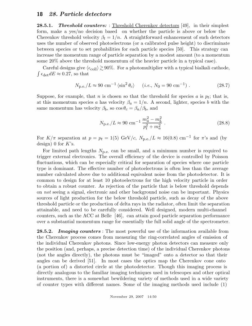
18 28. Particle detectors
28.5.1. Threshold counters: : Threshold Cherenkov detectors [49], in their simplestform, make a yes/no decision based on whether the particle is above or below theCherenkov threshold velocity βt = 1/n. A straightforward enhancement of such detectorsuses the number of observed photoelectrons (or a calibrated pulse height) to discriminatebetween species or to set probabilities for each particle species [50]. This strategy canincrease the momentum range of particle separation by a modest amount (to a momentumsome 20% above the threshold momentum of the heavier particle in a typical case).
Careful designs give 〈εcoll〉 90%. For a photomultiplier with a typical bialkali cathode,∫εdetdE ≈ 0.27, so that
Np.e./L ≈ 90 cm−1 〈sin2 θc〉 (i.e., N0 = 90 cm−1) . (28.7)
Suppose, for example, that n is chosen so that the threshold for species a is pt; that is,at this momentum species a has velocity βa = 1/n. A second, lighter, species b with thesame momentum has velocity βb, so cos θc = βa/βb, and
Np.e./L ≈ 90 cm−1 m2a − m2
b
p2t + m2
a. (28.8)
For K/π separation at p = pt = 1(5) GeV/c, Np.e./L ≈ 16(0.8) cm−1 for π’s and (bydesign) 0 for K’s.
For limited path lengths Np.e. can be small, and a minimum number is required totrigger external electronics. The overall efficiency of the device is controlled by Poissonfluctuations, which can be especially critical for separation of species where one particletype is dominant. The effective number of photoelectrons is often less than the averagenumber calculated above due to additional equivalent noise from the photodetector. It iscommon to design for at least 10 photoelectrons for the high velocity particle in orderto obtain a robust counter. As rejection of the particle that is below threshold dependson not seeing a signal, electronic and other background noise can be important. Physicssources of light production for the below threshold particle, such as decay of the abovethreshold particle or the production of delta rays in the radiator, often limit the separationattainable, and need to be carefully considered. Well designed, modern multi-channelcounters, such as the ACC at Belle [46], can attain good particle separation performanceover a substantial momentum range for essentially the full solid angle of the spectrometer.
28.5.2. Imaging counters : The most powerful use of the information available fromthe Cherenkov process comes from measuring the ring-correlated angles of emission ofthe individual Cherenkov photons. Since low-energy photon detectors can measure onlythe position (and, perhaps, a precise detection time) of the individual Cherenkov photons(not the angles directly), the photons must be “imaged” onto a detector so that theirangles can be derived [51]. In most cases the optics map the Cherenkov cone onto(a portion of) a distorted circle at the photodetector. Though this imaging process isdirectly analogous to the familiar imaging techniques used in telescopes and other opticalinstruments, there is a somewhat bewildering variety of methods used in a wide varietyof counter types with different names. Some of the imaging methods used include (1)
November 29, 2007 14:50

28. Particle detectors 19
focusing by a lens; (2) proximity focusing (i.e., focusing by limiting the emission regionof the radiation); and (3) focusing through an aperture (a pinhole). In addition, theprompt Cherenkov emission coupled with the speed of modern photon detectors allowsthe use of time imaging, a method which is used much less frequently in conventionalimaging technology. Finally, full tracking (and event reconstruction) can be performed inlarge water counters by combining the individual space position and time of each photontogether with the constraint that Cherenkov photons are emitted from each track at aconstant polar angle (Sec. 28.6 of this Review).
In a simple model of an imaging PID counter, the fractional error on the particlevelocity (δβ) is given by
δβ =σβ
β= tan θcσ(θc) , (28.9)
where
σ(θc) =〈σ(θi)〉√
Np.e.⊕ C , (28.10)
where 〈σ(θi)〉 is the average single photoelectron resolution, as defined by the optics,detector resolution and the intrinsic chromaticity spread of the radiator index ofrefraction averaged over the photon detection bandwidth. C combines a number of othercontributions to resolution including, (1) correlated terms such as tracking, alignment,and multiple scattering, (2) hit ambiguities, (3) background hits from random sources,and (4) hits coming from other tracks. In many practical cases, the resolution is limitedby these effects.
For a β ≈ 1 particle of momentum (p) well above threshold entering a radiator withindex of refraction (n), the number of σ separation (Nσ) between particles of mass m1
and m2 is approximately
Nσ ≈ |m21 − m2
2|2p2σ(θc)
√n2 − 1
. (28.11)
In practical counters, the angular resolution term σ(θc) varies between about 0.1 and5 mrad depending on the size, radiator, and photodetector type of the particular counter.The range of momenta over which a particular counter can separate particle speciesextends from the point at which the number of photons emitted becomes sufficient forthe counter to operate efficiently as a threshold device (∼20% above the threshold forthe lighter species) to the value in the imaging region given by the equation above. Forexample, for σ(θc) = 2mrad, a fused silica radiator(n = 1.474), or a flourocarbon gasradiator (C5F12, n = 1.0017), would separate π/K’s from the threshold region startingaround 0.15(3) GeV/c through the imaging region up to about 4.2(18) GeV/c at betterthan 3σ.
Many different imaging counters have been built during the last several decades [54].Among the earliest examples of this class of counters are the very limited acceptanceDifferential Cherenkov detectors, designed for particle selection in high momentum beamlines. These devices use optical focusing and/or geometrical masking to select particleshaving velocities in a specified region. With careful design, a velocity resolution ofσβ/β ≈ 10−4–10−5 can be obtained [49].
November 29, 2007 14:50

20 28. Particle detectors
Practical multi-track Ring-Imaging Cherenkov detectors (generically called RICHcounters) are a more recent development. They have been built in small-apertureand 4π geometries both as PID counters and as stand-alone detectors with completetracking and event reconstruction as discussed more fully below. PID RICH counters aresometimes further classified by ‘generations’ that differ based on performance, design,and photodetection techniques.
A typical example of a first generation RICH used at the Z factory e+e−colliders [52,53] has both liquid (C6F14, n = 1.276) and gas (C5F12, n = 1.0017)radiators, the former being proximity imaged using the small radiator thickness whilethe latter use mirrors. The phototransducers are a TPC/wire-chamber combinationhaving charge division or pads. They are made sensitive to photons by doping the TPCgas (usually, ethane/methane) with ∼ 0.05% TMAE (tetrakis(dimethylamino)ethylene).Great attention to detail is required, (1) to avoid absorbing the UV photons to whichTMAE is sensitive, (2) to avoid absorbing the single photoelectrons as they drift in thelong TPC, and (3) to keep the chemically active TMAE vapor from interacting withmaterials in the system. In spite of their unforgiving operational characteristics, thesecounters attained good e/π/K/p separation over wide momentum ranges during severalyears of operation. In particular, their π/K separation range extends over momenta fromabout 0.25 to 20 GeV/c.
Later generation counters [54] generally must operate at much higher particle ratesthan the first generation detectors, and utilize different photon detection bandwidths, withhigher readout channel counts, and faster, more forgiving photon detection technologythan the TMAE doped TPCs just described. Radiator choices have broadened to includematerials such as lithium flouride, fused silica, and aerogel. Vacuum based photodetectionsystems (e.g., single or multi anode photomultiplier tubes (PMT), multi channel platePMTs (MCP-PMT), or hybrid photodiodes (HPD)) have become increasingly common.They handle very high rates, may be used with a wide choice of radiators, and may besufficiently fast to allow time imaging or the use of time of flight information. Otherfast detection systems that use solid cesium iodide (CSI) photocathodes or triethylamine(TEA) doping in proportional chambers are useful with certain radiator types andgeometries.
A DIRC (Detector of Internally Reflected Cherenkov light) is a third generationsubtype of a RICH first used in the BaBar detector [47]. It “inverts” the usual principlefor use of light from the radiator of a RICH by collecting and imaging the total internallyreflected light, rather than the transmitted light. A DIRC utilizes the optical material ofthe radiator in two ways, simultaneously; first as a Cherenkov radiator, and second, as alight pipe for the Cherenkov light trapped in the radiator by total internal reflection. TheDIRC makes use of the fact that the magnitudes of angles are preserved during reflectionfrom a flat surface. This fact, coupled with the high reflection coefficients of the totalinternal reflection process (> 0.9995 for higly polished SiO2), and the long attenuationlength for photons in high purity fused silica, allows the photons of the ring image tobe transported to a detector outside the path of the particle where they may be imagedin up to three dimensions (two in space and one in time). The BaBar DIRC uses 144fused silica radiator bars (1.7 × 3.5 × 490 cm) with the light being focused onto 11 000
November 29, 2007 14:50

28. Particle detectors 21
conventional PMT’s located about 120 cm from the end of the bars by the “pinhole” ofthe bar end. DIRC performance can be understood using the formula for (Nσ) discussedabove. Typically, Np.e. is rather large (between 15 and 60) and the Cherenkov polar angleis measured to about 2.5 mrad. The momentum range with good π/K separation extendsup to about 4 GeV/c, matching the B decay momentum spectrum observed in BaBar.
28.6. Cherenkov tracking calorimeters
Written August 2003 by D. Casper (UC Irvine).
In addition to the specialized applications described in the previous section, Cherenkovradiation is also exploited in large, ring-imaging detectors with masses measuredin kilotons or greater. Such devices are not subdetector components, but completeexperiments with triggering, tracking, vertexing, particle identification and calorimetriccapabilities, where the large mass of the transparent dielectric medium serves as an activetarget for neutrino interactions (or their secondary muons) and rare processes like nucleondecay.
For volumes of this scale, absorption and scattering of Cherenkov light are non-negligible, and a wavelength-dependent factor e−d/L(λ) (where d is the distance fromemission to the sensor and L(λ) is the attenuation length of the medium) must beincluded in the integral of Eq. (28.4) for the photoelectron yield. The choice of mediumis therefore constrained by the refractive index and transparency in the region ofphotodetector sensitivity; highly-purified water is an inexpensive and effective choice;sea-water, mineral oil, polar ice, and D2O are also used. Photo-multiplier tubes (PMTs)on either a volume or surface lattice measure the time of arrival and intensity ofCherenkov radiation. Hemispherical PMTs are favored for the widest angular acceptance,and sometimes mounted with reflectors or wavelength-shifting plates to increase theeffective photosensitive area. Gains and calibration curves are measured with pulsed lasersignals transmitted to each PMT individually via optical fiber or applied to the detectoras a whole through one or more diffusing balls.
Volume instrumentation [55] is only cost-effective at low densities, with a spacingcomparable to the attenuation (absorption and scattering) length of Cherenkov lightin the medium (15–40 m for Antarctic ice and ∼45 m in the deep ocean). PMTs aredeployed in vertical strings as modular units which include pressure housings, front-endelectronics and calibration hardware. The effective photocathode coverage of such arraysis less than 1% but still adequate (using timing information and the Cherenkov angularconstraint) to reconstruct the direction of TeV muons to 1 or better. The size of such“neutrino telescopes” is limited only by cost once the technical challenges of deployment,power, signal extraction and calibration in an inaccessible and inhospitable environmentare addressed; arrays up to (1 km)3 in size are under study or development.
Surface instrumentation [56] allows the target volume to be viewed with higherphotocathode density by a number of PMTs which scales like (volume)2/3. To improvehermeticity and shielding, and to ensure that an outward-going particle’s Cherenkov coneilluminates sufficient PMTs for reconstruction, a software-defined fiducial volume beginssome distance (∼ 2 m) inside the photosensor surface. Events originating within the
November 29, 2007 14:50

22 28. Particle detectors
fiducial volume are classified as fully-contained if no particles exit the inner detector, orpartially-contained otherwise. An outer (veto) detector, optically separated from the innervolume and instrumented at reduced density, greatly assists in making this determinationand also simplifies the selection of contained events. The maximum size of a pure surfacearray is limited by the attenuation length (∼ 100 m has been achieved for large volumesusing reverse-osmosis water purification), pressure tolerance of the PMTs (< 80 metersof water, without pressure housings) and structural integrity of the enclosing cavity,if underground. In practice, these limitations can be overcome by a segmented designinvolving multiple modules of the nominal maximum size; megaton-scale devices areunder study.
Cherenkov detectors are excellent electromagnetic calorimeters, and the number ofCherenkov photons produced by an e/γ is nearly proportional to its kinetic energy.For massive particles, the number of photons produced is also related to the energy,but not linearly. For any type of particle, the visible energy Evis is defined as theenergy of an electron which would produce the same number of Cherenkov photons.The number of photoelectrons collected depends on a detector-specific scale factor, withevent-by-event corrections for geometry and attenuation. For typical PMTs, in waterNp.e. ≈ 15 ξ Evis(MeV), where ξ is the effective fractional photosensor coverage; for othermaterials, the photoelectron yield scales with the ratio of sin2 θc over density. At solarneutrino energies, the visible energy resolution (∼ 30%/
√ξ Evis(MeV)) is about 20%
worse than photoelectron counting statistics would imply. For higher energies, multi-photoelectron hits are likely and the charge collected by each PMT (rather the numberof PMTs firing) must be used; this degrades the energy resolution to approximately2%/
√ξ Evis(GeV). In addition, the absolute energy scale must be determined with
sources of known energy. Using an electron LINAC and/or nuclear sources, 0.5–1.5% hasbeen achieved at solar neutrino energies; for higher energies, cosmic-ray muons, Michelelectrons and π0 from neutrino interactions allow ∼ 3% absolute energy calibration.
A trigger can be formed by the coincidence of PMTs within a window comparable tothe detector’s light crossing time; the coincidence level thus corresponds to a visible energythreshold. Physics analysis is usually not limited by the hardware trigger, but rather theability to reconstruct events. The interaction vertex can be estimated using timing andrefined by applying the Cherenkov angle constraint to identified ring edges. Multi-ringevents are more strongly constrained, and their vertex resolution is 33–50% better thansingle rings. Vertex resolution depends on the photosensor density and detector size, withsmaller detectors performing somewhat better than large ones (∼ 25 cm is typical forexisting devices). Angular resolution is limited by multiple scattering at solar neutrinoenergies (25–30) and improves to a few degrees around Evis = 1 GeV.
A non-showering (µ, π±, p) track produces a sharp ring with small contributions fromdelta rays and other radiated secondaries, while the more diffuse pattern of a showering(e, γ) particle is actually the superposition of many individual rings from charged showerproducts. Using maximum likelihood techniques and the Cherenkov angle constraint,these two topologies can be distinguished with an efficiency which depends on thephotosensor density and detector size [57]. This particle identification capability hasbeen confirmed by using cosmic-rays and Michel electrons, as well as charged-particle [58]
November 29, 2007 14:50

28. Particle detectors 23
and neutrino [59] beams. Large detectors perform somewhat better than smaller oneswith identical photocathode coverage; a misidentification probability of ∼ 0.4%/ξin the sub-GeV range is consistent with the performance of several experiments for4% < ξ < 40%. Detection of a delayed coincidence from muon decay offers another, moreindirect, means of particle identification; with suitable electronics, efficiency approaches100% for µ+ decays but is limited by nuclear absorption (22% probability in water)for µ−.
Reconstruction of multiple Cherenkov rings presents a challenging pattern recognitionproblem, which must be attacked by some combination of heuristics, maximum likelihoodfitting, Hough transforms and/or neural networks. The problem itself is somewhatill-defined since, as noted, even a single showering primary produces many closely-overlapping rings. For π0 → γγ two-ring identification, performance falls off rapidly withincreasing π0 momentum, and selection criteria must be optimized with respect to theanalysis-dependent cost-function for e ↔ π0 mis-identification. Two representative casesfor ξ = 39% will be illustrated. In an atmospheric neutrino experiment, where π0 arerelatively rare compared to e±, one can isolate a > 90% pure 500 MeV/c π0 sample withan efficiency of ∼ 40%. In a νe appearance experiment at Eν ≤ 1 GeV, where e± arerare compared to π0, a 99% pure 500 MeV/c electron sample can be identified with anefficiency of ∼ 70%. For constant ξ, a larger detector (with, perforce, a greater number ofpixels to sample the light distribution) performs somewhat better at multi-ring separationthan a smaller one. For a more detailed discussion of event reconstruction techniques, seeRef. 48.
Table 28.5: Properties of Cherenkov tracking calorimeters. LSND was a hybridscintillation/Cherenkov detector; the estimated ratio of isotropic to Cherenkovphotoelectrons was about 5:1. MiniBooNE’s light yield also includes a smallscintillation component.
Detector Fiducial mass PMTs ξ p.e./ Dates(kton) (diameter, cm) MeV
IMB-1 [60] 3.3 H2O 2048 (12.5) 1% 0.25 1982–85IMB-3 [61] 3.3 H2O 2048 (20 +plate) 4.5% 1.1 1987–90KAM I [62,63] 0.88/0.78 H2O 1000/948 (50) 20% 3.4 1983–85KAM II [64] 1.04 H2O 948 (50) 20% 3.4 1986–90LSND [65] 0.084 oil+scint. 1220 (20) 25% 33 1993–98SK-1 [66] 22.5 H2O 11146 (50) 39% 6 1997–2001SK-2 22.5 H2O 5182 (50) 18% 3 2002–K2K [67] 0.025 H2O 680 (50) 39% 6 1999–SNO [68] 1.0 D2O 9456 (20+cone) 55% 9 1999–MiniBooNE 0.445 oil 1280 (20) 10% 3–4 2002–
November 29, 2007 14:50

24 28. Particle detectors
28.7. Gas-filled detectors
28.7.1. Wire chambers : Written October 1999 by A. Cattai and G. Rolandi(CERN).
A wire chamber relies on the detection of a large fraction of the charge created in avolume filled with an appropriate gas mixture. A charged particle traversing a gas layerof thickness ∆ produces electron-ion pairs along its path (see Sec. 27.2). The yield (1/λ)of ionization encounters for a minimum ionization particle (m.i.p.) (see Fig. 27.1) is givenin Table 28.6.
Encounters/cm t99(mm) Free electrons/cm
He 5 9.2 16Ne 12 3.8 42Ar 25 1.8 103Xe 46 1.0 340CH4 27 1.7 62CO2 35 1.3 107C2H6 43 1.1 113
Table 28.6: For various gases at STP: (a) yield of ionization encounters (1/λ) form.i.p. [69], (b) t99: thickness of the gas layer for 99% efficiency, and (c) the averagenumber of free electrons produced by a m.i.p. (calculated using data from Ref. 70).
The probability to have at least one ionization encounter is 1 − exp(−∆/λ) and thethickness of the gas layer for 99% efficiency is t99 = 4.6λ. Depending on the gas, some65–80% of the encounters result in the production of only one electron; the probabilitythat a cluster has more than five electrons is smaller than 10%. However the tail of thedistribution is very long and the yield of ionization electrons is 3–4 times that of theionization encounters. The secondary ionization happens either in collisions of (primary)ionization electrons with atoms or through intermediate excited states. The process isnon-linear and gas mixtures may have larger yields than each of their components. Seealso the discussion in Sec. 27.7.
Under the influence of electric and magnetic fields the ionization electrons drift insidethe gas with velocity u given by:
u = µ|E| 11 + ω2τ2
(E + ωτ(E× B) + ω2τ2(E · B)B
)(28.12)
where E and B are unit vectors in the directions of the electric and magnetic fieldsrespectively, µ is the electron mobility in the gas, ω is the cyclotron frequency eB/mc, andτ = µm/e is the mean time between collisions of the drifting electrons. The magnitude ofthe drift velocity depends on many parameters; typical values are in the range 1–8 cm/µs.
November 29, 2007 14:50

28. Particle detectors 25
In a quite common geometry, the drift electric field is perpendicular to the magneticfield. In this case the electrons drift at an angle ψ with respect to the electric fielddirection such that tanψ = ωτ .
The ionization electrons are eventually collected by a thin (typically 10 µm radius)anode wire where a strong electric field—increasing as 1/r—accelerates the electronsenough to produce secondary ionization and hence an avalanche. A quenching gas(organic molecules with large photo-absorption cross-section) absorbs the majority ofthe photons produced during the avalanche development, keeping the avalanche regionlocalized. The gain achievable with a wire counter depends exponentially on the chargedensity on the wire, on the gas density ρ and—through it—on pressure and temperature:dG/G ≈ −Kdρ/ρ, where the coefficient K ranges between 5 and 8 in practical cases.Gains larger than 104 can be obtained in proportional mode.
The electrons produced in the avalanche are collected by the wire in a few nanoseconds.The positive ions move away from the wire and generate a signal that can be detectedwith an amplifier. Depending on whether the wire is treated as a current source or avoltage source, the signal is described respectively by:
I(t) = qd
dtF (t) ; ∆V (t) =
q
CF (t) , (28.13)
where q is the positive charge in the avalanche, C is the capacitance between the anodewire and the cathodes and F (t) = ln(1 + t/t0)/ ln(1 + tmax/t0). The constant t0 is of theorder of one or few nanoseconds; the constant tmax (several microseconds) describes thetime that it takes ions to reach the cathodes.
A sketch of the first multi-wire proportional chamber (MWPC) [71] is shown inFig. 28.3. It consists of a plane of parallel sense wires with spacing s and length Linserted in a gap of thickness ∆. The potential distributions and fields in a proportionalor drift chamber can usually be calculated with good accuracy from the exact formula forthe potential around an array of parallel line charges q (coul/m) along z and located aty = 0, x = 0, ±s, ±2s, . . . ,
V (x, y) = − q
4π ε0ln
4
[sin2
(πx
s
)+ sinh2
(πy
s
)]. (28.14)
With digital readout, the resolution in the direction perpendicular to the wire iss/√
12, where s is typically 1–2 mm. Similar resolution can be achieved with a smallerchannel density by measuring the difference in time between the arrival of electrons atthe wire and the traversal of the particle, albeit with a longer response time. In the caseof drift chambers, the spatial resolution is limited by the diffusion of ionization electronsduring the drift and by the fluctuations of the ionization process. Depending on the gasmixture, the width of the diffusing cloud after 1 cm of drift is typically between 50 and300 µm; small diffusion implies low drift velocity. With drift lengths up to 5 cm (1 µs),resolutions in the range 100–200 µm have been achieved in chambers with surface areas ofseveral square meters [73]. The central detectors in many collider experiments are driftchambers with the wires parallel to the beam direction. Small volume chambers (0.1 m3)
November 29, 2007 14:50

26 28. Particle detectors
–0.6 –0.4 –0.2 0.2 0.4 0.60–0.4
–0.3
–0.2
–0.1
0
0.1
0.2
0.3
0.4
x (cm)
y (c
m)
Figure 28.3: Electric field lines in a (MWPC) with an anode pitch of 2 mm ascalculated with GARFIELD program [72].
have been used for vertex measurement achieving resolutions of 50 µm using high pressure(2–4 bar) and low diffusion gas mixtures [74]. Large volume chambers (5–40 m3) withseveral thousand wires of length of 1–2 meters are operated with resolution between 100and 200 µm [75].
The spatial resolution cannot be improved by arbitrarily reducing the spacing of thewires. In addition to the practical difficulties of precisely stringing wires at a pitch below1 mm, there is a fundamental limitation: the electrostatic force between the wires isbalanced by the mechanical tension, which cannot exceed a critical value. This gives thefollowing approximate stability condition:
s
L≥ 1.5 × 10⁻³V (kV)
√20 gT
, (28.15)
where V is the voltage of the sense wire and T is the tension of the wire in grams-weightequivalent.
A review of the principle of particle detection with drift chambers can be found in [76].A compilation of the mobilities, diffusion coefficients and drift deflection angles as afunction of E and B for several gas mixtures used in proportional chambers can be foundin [77]. A review of micro-strip gas chambers (MSGC) can be found in [78].
November 29, 2007 14:50
28. Particle detectors 27
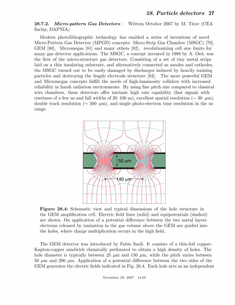
28.7.2. Micro-pattern Gas Detectors : Written October 2007 by M. Titov (CEASaclay, DAPNIA)
Modern photolithographic technology has enabled a series of inventions of novelMicro-Pattern Gas Detector (MPGD) concepts: Micro-Strip Gas Chamber (MSGC) [79],GEM [80], Micromegas [81] and many others [82], revolutionizing cell size limits formany gas detector applications. The MSGC, a concept invented in 1988 by A. Oed, wasthe first of the micro-structure gas detectors. Consisting of a set of tiny metal stripslaid on a thin insulating substrate, and alternatively connected as anodes and cathodes,the MSGC turned out to be easily damaged by discharges induced by heavily ionizingparticles and destroying the fragile electrode structure [83]. The more powerful GEMand Micromegas concepts fulfill the needs of high-luminosity colliders with increasedreliability in harsh radiation environments. By using fine pitch size compared to classicalwire chambers, these detectors offer intrinsic high rate capability (fast signals withrisetimes of a few ns and full widths of 20–100 ns), excellent spatial resolution (∼ 30 µm),double track resolution (∼ 500 µm), and single photo-electron time resolution in the nsrange.
140 µm
50 µm
Figure 28.4: Schematic view and typical dimensions of the hole structure inthe GEM amplification cell. Electric field lines (solid) and equipotentials (dashed)are shown. On application of a potential difference between the two metal layerselectrons released by ionization in the gas volume above the GEM are guided intothe holes, where charge multiplication occurs in the high field.
The GEM detector was introduced by Fabio Sauli. It consists of a thin-foil copper-Kapton-copper sandwich chemically perforated to obtain a high density of holes. Thehole diameter is typically between 25 µm and 150 µm, while the pitch varies between50 µm and 200 µm. Application of a potential difference between the two sides of theGEM generates the electric fields indicated in Fig. 28.4. Each hole acts as an independent
November 29, 2007 14:50

28 28. Particle detectors
proportional counter; electrons released by the ionization in the gas drift into the holeand multiply in the high electric field (50–70 kV/cm). Most of avalanche electronsare transferred into the gap below the GEM. Distributing the avalanche multiplicationamong several cascading electrodes allows the multi-GEM detectors to operate at overallgas gain above 104 in the presence of highly ionizing particles, while eliminating therisk of discharges (< 10−12 per hadron). This is the major advantage of the GEMtechnology [84]. A unique property of the GEM detector is the complete decoupling ofthe amplification stage (GEM) and the readout electrode (PCB), which operates at unitygain and serves only as a charge collector.
HV1
HV2Micromesh
100 µ
m
Anode plane
e−
E2
40 kV/cm
Particle
Drift gap
Amplificationgap
Figure 28.5: Schematic drawing and typical dimensions of the Micromegasdetector. Charges produced in the drift gap are drifting to the small amplificationregion, limited by the mesh and the anode, where they are amplified.
Ioannis Giomataris introduced the micro-mesh gaseous structure (Micromegas), whichis a parallel-plate avalanche counter (Fig. 28.5). It consists of a few mm drift region(electric field ∼1 kV/cm) and a narrow multiplication gap (25-150 µm, 50–70 kV/cm),located between a thin metal grid (micromesh) and the readout electrode (strips/padsof conductor printed on an insulator board). The electric field is homogeneous both inthe drift and amplification gaps. Due to the narrow multiplication region in Micromegas,locally small variations of the amplification gap are compensated by an inverse variationof the amplification coefficient and therefore do not induce gain fluctuations. The smallamplification gap is a key element in Micromegas operation, giving rise to its excellentspatial resolution: 12 µm accuracy (limited by the the micromesh pitch) for MIPs [85],and very good energy resolution (∼12% FWHM with 6 keV x rays).
Over the past decade GEM and Micromegas detectors have become increasinglyimportant. COMPASS is a first high-luminosity experiment at CERN which pioneeredthe use of large-area (∼ 40 × 40 cm2) GEM and Micromegas detectors for high-rateparticle tracking, reaching 25 kHz/mm2 in the near-beam area. Both technologies haveachieved a tracking efficiency of close to 100% at gas gains of about 104, a spatialresolution of 70–100 µm and a time resolution of ∼ 10 ns. GEMs have entered theLHC program; they will be used for triggering in the LHCb Muon System and in theTOTEM Telescopes. A time projection chamber (TPC) using GEM or Micromegas as a
November 29, 2007 14:50

28. Particle detectors 29
gas amplification device is also one of the main options for a high-precision tracking atthe International Linear Collider (ILC).
The performance and robustness of MPGDs have encouraged their applications inhigh-energy and neutrino physics, astrophysics, UV and visible photon detection, nuclearphysics and neutron detection domain, radiation therapy and electronic portal imagingdevices. A big step in the direction of the industrial manufacturing of large-size MPGDs isthe development of the “bulk” Micromegas technology [86]. The basic idea is to build thewhole detector in a single process: the anode plane with copper strips, a photo-imageablepolyimide film and the woven mesh are laminated together at a high temperature forminga single object. Employing the “bulk” technology, 72 large Micromegas (34 × 36 cm2)planes with an active area of 9 m2 are being built for the T2K TPC detector.
Sensitive and low-noise electronics will enlarge the range of the MPGD applications.Recently, GEM and Micromegas were read out by high-granularity (50 µm pitch) CMOSpixel chips assembled directly below the GEM or Micromegas amplification structureand serving as an integrated charge collecting anode [87,88,89]. With this arrangementavalanche electrons are collected on the top metal layer of the CMOS ASIC; everyinput pixel is then directly connected to the amplification, digitization and sparsificationcircuits integrated in the underlying active layers of the CMOS technology. GEM coupledto a VLSI pixel array could serve as a highly efficient x-ray polarimeter, which is able toreconstruct simultaneously initial direction and dynamics of photoelectron energy loss forthe low energy (<10 keV) x rays. A fine-pitch GEM matching the pitch of pixel ASIC(50 µm) allows to achieve a superior single-electron avalanche reconstruction accuracyof 4 µm, which makes it suitable candidate for fast gas photo-multipliers. For minimumionizing particle tracks a spatial resolution down to 20 µm was achieved with Medipix2and Timepix CMOS chips coupled to Micromegas and GEM devices. An attractivesolution for the construction of MPGDs with pixel anode readout is the integration ofthe Micromegas amplification and CMOS chip by means of the “wafer post-processing”technology. The sub-µm precision of the grid dimensions and avalanche gap size results ina uniform gas gain; the grid hole size, pitch and pattern can be easily adapted to matchthe geometry of any pixel readout chip.
Recent developments in radiation hardness research with state-of-the-art MPGDs arereviewed in Ref. 90. Better properties of MPGDs, which are rather insensitive to agingcompared to wire chambers, can be explained by the separation of multiplication (GEMor parallel plate Micromegas amplification) and anode readout structures, and the lowerelectric field strength (∼ 50 kV/cm) in the multiplication region, compared to the anodewire surface field (∼ 250 kV/cm).
November 29, 2007 14:50
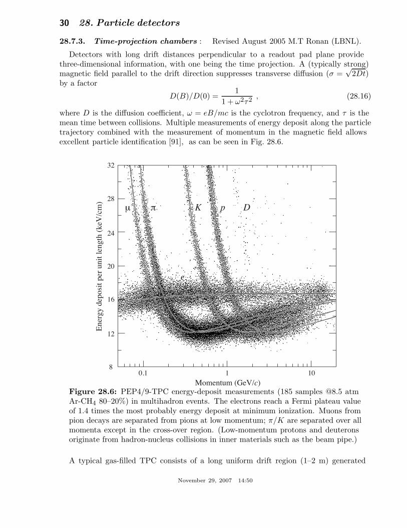
30 28. Particle detectors
28.7.3. Time-projection chambers : Revised August 2005 M.T Ronan (LBNL).
Detectors with long drift distances perpendicular to a readout pad plane providethree-dimensional information, with one being the time projection. A (typically strong)magnetic field parallel to the drift direction suppresses transverse diffusion (σ =
√2Dt)
by a factor
D(B)/D(0) =1
1 + ω2τ2, (28.16)
where D is the diffusion coefficient, ω = eB/mc is the cyclotron frequency, and τ is themean time between collisions. Multiple measurements of energy deposit along the particletrajectory combined with the measurement of momentum in the magnetic field allowsexcellent particle identification [91], as can be seen in Fig. 28.6.
µ π K p
e
D
e
Ene
rgy
depo
sit p
er u
nit l
engt
h (k
eV/c
m)
Momentum (GeV/c)
8
12
16
20
24
28
32
0.1 1 10
Figure 28.6: PEP4/9-TPC energy-deposit measurements (185 samples @8.5 atmAr-CH4 80–20%) in multihadron events. The electrons reach a Fermi plateau valueof 1.4 times the most probably energy deposit at minimum ionization. Muons frompion decays are separated from pions at low momentum; π/K are separated over allmomenta except in the cross-over region. (Low-momentum protons and deuteronsoriginate from hadron-nucleus collisions in inner materials such as the beam pipe.)
A typical gas-filled TPC consists of a long uniform drift region (1–2 m) generated
November 29, 2007 14:50

28. Particle detectors 31
by a central high-voltage membrane and precision concentric cylindrical field cageswithin a uniform, parallel magnetic field [76]. A multiwire proportional plane, GasElectron Multiplier (GEM) [92] or Micromegas [93] micropattern device providesprimary electron gas amplification. Details of construction and electron trajectoriesfor a multiwire proportional anode plane are shown in Fig. 28.7. Signal shaping andprocessing using analog storage devices or FADC’s allows excellent pattern recognition,track reconstruction, and particle identification within the same detector.
Typical values:
Gas: Ar + (10–20%) CH4 Pressure(P ) = 1–8.5 atm.
E/P = 100–200 V /cm/atm B = 1–2 Tesla
vdrift = 5–7 cm/µs ωτ = 1–8
σx or y = 100–200 µm σz = 0.2–1 mm
σE dep = 2.5–5.5 %
Truncated mean energy-deposit resolution depends on the number and size of samples,and gas pressure:
σE dep ∝ N−0.43 × (P)−0.32 . (28.17)
Here N is the number of samples, is the sample size, and P is the pressure. Typicalenergy-deposit distributions are shown in Fig. 28.6. Good three-dimensional two-trackresolutions of about 1–1.5 cm are routinely achieved.
E × B distortions arise from nonparallel E and B fields (see Eq. (28.12)), and fromthe curved drift of electrons to the anode wires in the amplification region. Positionmeasurement errors include contributions from the anode-cathode geometry, the trackcrossing angle (α), E × B distortions, and from the drift diffusion of electrons
σ2x or y = σ2
0 + σ2D(1 + tan2 α)L/Lmax + σ2
α(tanα − tanψ)2 (28.18)
where σ is the coordinate resolution, σ0 includes the anode-cathode geometry contribution,ψ is the Lorentz angle, and L is the drift distance.
Space-charge distortions arise in high-rate environments, especially for low values of ωτ .However, they are mitigated by an effective gating grid (Fig. 28.7). Field uniformities of∫
(E⊥/E) dz 0.5–1 mm , (28.19)
over 10–40 m3 volumes have been obtained. Laser tracks and calibration events allowmapping of any remnant drift non-uniformities.
November 29, 2007 14:50

32 28. Particle detectors
–0.6 –0.4 –0.2 0.20 0.4 0.6x (cm)
y (c
m)
y (c
m)
0.6
0.8
2.0
1.0
1.2
1.4
1.6
1.8
0.4
0.6
0.8
1.0
1.2
1.4
1.6
1.8 (b) Gating grid open
(a) Gating grid closed
gating grid
shielding grid
anode wires
cathode plane
+− +− +− −
Figure 28.7: (a) Drifting electrons are collected on the gating grid until gatedopen by a triggering event. A shielding grid at ground potential is used to terminatethe drift region. Electrons drifting through an open gating grid (b) pass throughto the amplification region around the anode wires. Positive ions generated in theavalanche are detected on segmented cathode pads to provide precise measurementsalong the wire. The slow positive ions are blocked from entering the drift region byclosing the gating grid after the electrons have drifted through.
November 29, 2007 14:50

28. Particle detectors 33
28.7.4. Transition radiation detectors (TRD’s) : Written August 2007 byP. Nevski (BNL), A. Romaniouk (Moscow Eng. & Phys. Inst.)
Transition radiation (TR) x rays are produced when a highly relativistic particle(γ >∼ 103) crosses a refractive index interface, as discussed in Sec. 27.7. The x rays,ranging from a few keV to a few dozen keV, are emitted at a characteristic angle 1/γfrom the particle trajectory. Since the TR yield is about 1% per boundary crossing,radiation from multiple surface crossings is used in practical detectors. In the simplestconcept, a detector module might consist of low-Z foils followed by a high-Z active layermade of proportional counters filled with a Xe-rich gas mixture. The atomic numberconsiderations follow from the dominant photoelectric absorption cross section per atomgoing roughly as Z n/E3
x, where n varies between 4 and 5 over the region of interest, andthe x-ray energy is Ex.* To minimize self-absorption, materials such as polypropylene,Mylar, carbon, and (rarely) lithium are used as radiators. The TR signal in the activeregions is in most cases superimposed upon the particle’s ionization losses. These drop alittle faster than Z/A with increasing Z, providing another reason for active layers withhigh Z.
The TR intensity for a single boundary crossing always increases with γ, but formultiple boundary crossings interference leads to saturation near a Lorentz factorγ sat = 0.6 ω1
√12/c [94,95], where ω1 is the radiator plasma frequency, 1 is its
thickness, and 2 the spacing. In most of the detectors used in particle physics theradiator parameters are chosen to provide γ sat ≈ 2000. Those detectors normally workas threshold devices, ensuring the best electron/pion separation in the momentum range1 GeV/c <∼ p <∼ 150 GeV/c.
One can distinguish two design concepts—“thick” and “thin” detectors:1. The radiator, optimized for a minimum total radiation length at maximum TR yield
and total TR absorption, consists of few hundred foils (for instance 300 20 µm thickpolypropylene foils). A dominant fraction of the soft TR photons is absorbed in theradiator itself. To increase the average TR photon energy further, part of the radiatorfar from the active layers is often made of thicker foils. The detector thickness, about2 cm for Xe-filled gas chambers, is optimized to absorb the shaped x-ray spectrum.A classical detector is composed of several similar modules which respond nearlyindependently. Such detectors were used in the NA34 [96], NOMAD [97], and arebeing used in the ALICE [98] experiment.
2. In another TRD concept a fine granular radiator/detector structure exploits the softpart of the TR spectrum more efficiently. This can be achieved, for instance, bydistributing small-diameter straw-tube detectors uniformly or in thin layers throughoutthe radiator material (foils or fibers). Even with a relatively thin radiator stack,radiation below 5 keV is mostly lost in the radiators themselves. However for photonenergies above this value the absorption becomes smaller and the radiation can beregistered by several consecutive detector layers, thus creating a strong TR build-upeffect. Examples of the detectors using this approach can be found in both accelerator
* Photon absorption coefficients for the elements (via a NIST link), and dE/dx|min andplasma energies for many materials are given in pdg.lbl.gov/AtomicNuclearProperties.
November 29, 2007 14:50

34 28. Particle detectors
(ATLAS [99]) and space (PAMELA [100], AMS [101]) experiments. For example, inthe ATLAS TR tracker charged particles cross about 35 effective straw tube layersembedded in the radiator material. The effective thickness of the Xe gas per straw isabout 2.3 mm and the average number of foils per straw is about 40 with an effectivefoil thickness of about 20 µm.Both TR photon absorption and the TR build-up significantly affect the detector
performance. Although the values mentioned above are typical for most of the plasticradiators used with Xe-based detectors, they vary significantly depending on detectorparameters: radiator material, thickness and spacing, the construction of the sensitivechambers, their position, etc. Thus careful simulations are usually needed to build adetector optimized for a particular application.
The discrimination between electrons and pions can be based on the charge depositionmeasured in each detection module, on the number of clusters—energy depositionsobserved above an optimal threshold (usually in the 5 to 7 keV region), or on moresophisticated methods analyzing the pulse shape as a function of time. The total energymeasurement technique is more suitable for thick gas volumes, which absorb most of theTR radiation and where the ionization loss fluctuations are small. The cluster-countingmethod works better for detectors with thin gas layers, where the fluctuations of theionization losses are big. Cluster-counting replaces the Landau-Vavilov distribution ofbackground ionization energy losses with the Poisson statistics of δ-electrons, responsiblefor the distribution tails. The latter distribution is narrower that the Landau-Vavilovdistribution.
The major factor in the performance of any TRD is its overall length. This isillustrated in Fig. 28.8, which shows, for a variety of detectors, the pion efficiencyat a fixed electron efficiency of 90% as a function of the overall detector length. Theexperimental data, covering a range of particle energies from a few GeV to 40 GeV, arerescaled to an energy of 10 GeV when possible. Phenomenologically, the rejection poweragainst pions increases as 5 · 10L/38, where the range of validity is L ≈ 20–100 cm.
Many recent TRDs combine particle identification with charged-track measurementin the same detector [98,99]. This provides a powerful tool for electron identificationeven at very high particle densities. Another example of this combination is described inRef. 102. In this work Si-microstrip detectors operating in a magnetic filed are used bothfor particle and TR detection. The excellent coordinate resolution of the Si detectorsallows spatial separation of the TR photons from particle ionization tracks with relativelymodest distances between radiator and detector.
Recent TRDs for particle astrophysics are designed to directly measure the Lorentzfactor of high-energy nuclei by using the quadratic dependence of the TR yield on nuclearcharge [103,104]. The radiator configuration (1, 2) is tuned to extend the TR yield riseup to γ <∼ 105 using more energetic part of the TR spectrum (up to 100 keV). Exoticradiator materials such as aluminum and unusual TR detection methods (Comptonscattering) are used such cases [103].
November 29, 2007 14:50

28. Particle detectors 35
0.01
0.1
0.001
10 20 50 200100
NA34 (HELIOS)C.Fabjan et al.R 806A. Bungener et al.ZEUS
KEKUA2H.Butt et al.D0M.Holder et al.H.WeidkampH.Grssler et al.ATLASNOMADAMS
Total detector length (cm)
Pion
eff
icie
ncy
ALICEPAMELA
:
Figure 28.8: Pion efficiency measured (or predicted) for different TRDs as afunction of the detector length for a fixed electron efficiency of 90%. The plot istaken from [96] with efficiencies of more recent detectors [99–100] added (ATLAS toPAMELA).
28.7.5. Resistive-plate chambers : Revised September 2007 by H.R. Band (U.Wisconsin).
The resistive-plate chamber (RPC) was developed by Santonico and Cardarelli in theearly 1980’s [105] as a low-cost alternative to large scintillator planes.* Most commonly,an RPC is constructed from two parallel high-resistivity (109–1013 Ω-cm) glass or phenolic(Bakelite)/melamine laminate plates with a few-mm gap between them which is filledwith atmospheric-pressure gas. The gas is chosen to absorb UV photons in order to limittransverse growth of discharges. The backs of the plates are coated with a lower-resistivitypaint or ink (∼105 Ω/), and a high potential (7–12 kV) is maintained between them.The passage of a charged particle initiates an electric discharge, whose size and durationare limited since the current reduces the local potential to below that needed to maintainthe discharge. The sensitivity of the detector outside of this region is unaffected. Thesignal readout is via capacitive coupling to metallic strips on both sides of the detectorwhich are separated from the high voltage coatings by thin insulating sheets. The x andy position of the discharge can be measured if the strips on opposite sides of the gap areorthogonal. When operated in streamer mode, the induced signals on the strips can bequite large (∼300 mV), making sensitive electronics unnecessary. An example of an RPC
* It was based on earlier work on a spark counter with one high-resistivity plate [106].
November 29, 2007 14:50

36 28. Particle detectors
structure is shown in Fig. 28.9.
Aluminumx pickup strips
y pickup strips
Insulator
2 mm
GraphiteInsulator
SpacersAluminum
HV Foam
Bakelite
BakeliteGas
Foam
Graphite
2 mm2 mm
1 mm
1 cm
Figure 28.9: Schematic cross section of a typical RPC, in this case the single-gapstreamer-mode BaBar RPC.
RPC’s have inherent rate limitations since the time needed to re-establish the fieldafter a discharge is proportional to the chamber capacitance and plate resistance. Theaverage charge per streamer is 100–1000 pC. Typically, the efficiency of streamer-modeglass RPC’s begins to fall above ∼0.4 Hz/cm2. Because of Bakelite’s lower bulk resistivity,Bakelite RPC’s can be efficient at 10–100 Hz/cm2. The need for higher rate capabilityled to the development of avalanche-mode RPC’s, in which the gas and high voltage havebeen tuned to limit the growth of the electric discharge, preventing streamer formation.Typical avalanche-mode RPC’s have a signal charge of about 10 pC and can be efficientat 1 kHz/cm2. The avalanche discharge produces a much smaller induced signal on thepickup strips (∼1 mV) than streamers, and thus requires a more sophisticated and carefulelectronic design.
Many variations of the initial RPC design have been built for operation in eithermode. Efficiencies of >∼ 92% for single gaps can be improved by the use of two ormore gas gaps with shared pickup strips. Non-flammable and more environmentallyfriendly gas mixtures have been developed. In streamer mode, various mixtures of argonwith isobutane and tetrafluoroethane have been used. For avalanche mode operation,a gas mixture of tetrafluoroethane (C2H2F4) with 2–5% isobutane and 0.4–10% sulfurhexafluoride (SF6) is typical. An example of large-scale RPC use is provided by the muonsystem being built for the ATLAS detector, where three layers of pairs of RPC’s are usedto trigger the drift tube arrays between the pairs. The total area is about 10,000m2.These RPC’s provide a spatial resolution of 1 cm and a time resolution of 1 ns at anefficiency ≥ 99%.
Developments of multiple-gap RPC’s [107] lead to RPC designs with much bettertiming resolution (∼ 50 ps) for use in time-of-flight particle identification systems. Apioneering design used by the HARP experiment [108] has two sets of 2 thin gas gaps(0.3mm) separated by thin(0.7mm) glass plates. The outer plates are connected to high
November 29, 2007 14:50
28. Particle detectors 37
voltage and ground while the inner plate is electrically isolated and floats to a stableequilibrium potential. The observed RPC intrinsic time resolution of 127 ps may havebeen limited by amplifier noise. Fonte provides useful review [109] of other RPC designs.
Operational experience with RPC’s has been mixed. Several experiments (e.g., L3 andHARP) have reported reliable performance. However, the severe problems experiencedwith the BaBar RPC’s have raised concerns about the long-term reliability of BakeliteRPC’s.
Glass RPC’s have had fewer problems, as seen by the history of the BELLE chambers.A rapid growth in the noise rate and leakage current in some of the BELLE glass RPC’swas observed during commissioning. It was found that water vapor in the input gas wasreacting with fluorine (produced by the disassociation of the tetrafluoroethane in thestreamers) to produce hydrofluoric acid. The acid etched the glass surfaces, leading toincreased noise rates and lower efficiencies. The use of copper gas piping to insure thedryness of the input gas stopped the problem. The BELLE RPC’s have now operatedreliably for more than 5 years.
Several different failure modes diagnosed in the first-generation BaBar Bakelite RPC’scaused the average efficiency of the barrel RPC’s to fall from >∼ 90% to 35% in five years.The linseed oil which is used in Bakelite RPC’s to coat the inner surface [110] had notbeen completely cured. Under warm conditions (32 C) and high voltage, oil collectedon the spacers between the gaps or formed oil-drop bridges between the gaps. This ledto large leakage currents (50–100µA in some chambers) which persisted even when thetemperature was regulated at 20 C. In addition, the graphite layer used to distribute thehigh voltage over the Bakelite became highly resistive (100kΩ/ → 10MΩ/), resultingin lowered efficiency in some regions and the complete death of whole chambers.
The BaBar problems and the proposed use of Bakelite RPC’s in the LHC detectorsprompted detailed studies of RPC aging and have led to improved construction techniquesand a better understanding of RPC operational limits. The graphite layer has beenimproved and should be stable with integrated currents of <∼ 600mC/cm2. Molded gasinlets and improved cleanliness during construction have reduced the noise rate of newchambers. Unlike glass RPC’s, Bakelite RPC’s have been found to require humid inputgases to prevent drying of the Bakelite (increasing the bulk resistivity) which woulddecrease the rate capability. Second-generation BaBar RPC’s incorporating many of theabove improvements have performed reliably for over two years [111].
With many of these problems solved, new-generation RPC’s are now being or soon willbe used in about a dozen cosmic-ray and HEP detectors. Their comparatively low cost,ease of construction, good time resolution, high efficiency, and moderate spatial resolutionmake them attractive in many situations, particularly those requiring fast timing and/orlarge-area coverage.
November 29, 2007 14:50

38 28. Particle detectors
28.8. Silicon semiconductor detectors
Updated September 2007 by H. Spieler (LBNL).
Semiconductor detectors are widely used in modern high-energy physics experiments.They are the key ingredient of high-resolution vertex and tracking detectors and are alsoused as photodetectors in scintillation calorimeters. The most commonly used material issilicon, but germanium, gallium-arsenide, CdTe, CdZnTe, and diamond are also usefulin some applications. Integrated circuit technology allows the formation of high-densitymicron-scale electrodes on large (10–15 cm diameter) wafers, providing excellent positionresolution. Furthermore, the density of silicon and its small ionization energy result inadequate signals with active layers only 100–300 µm thick, so the signals are also fast(typically tens of ns). Semiconductor detectors depend crucially on low-noise electronics(see Sec. 28.9), so the detection sensitivity is determined by signal charge and capacitance.For a comprehensive discussion of semiconductor detectors and electronics see Ref. 112.
Silicon detectors are p-n junction diodes operated at reverse bias. This forms asensitive region depleted of mobile charge and sets up an electric field that sweeps chargeliberated by radiation to the electrodes. Detectors typically use an asymmetric structure,e.g. a highly doped p electrode and a lightly doped n region, so that the depletion regionextends predominantly into the lightly doped volume.The thickness of the depleted region is
W =√
2ε (V + Vbi)/Ne =√
2ρµε(V + Vbi) , (28.20)
where V = external bias voltageVbi = “built-in” voltage (≈ 0.5 V for resistivities typically used in detectors)N = doping concentratione = electronic chargeε = dielectric constant = 11.9 ε0 ≈ 1 pF/cmρ = resistivity (typically 1–10 kΩ cm)µ = charge carrier mobility
= 1350 cm2 V−1 s−1 for electrons= 450 cm2 V−1 s−1 for holes
or
W = 0.5 [µm/√
Ω-cm · V] ×√
ρ(V + Vbi) for n-type material, and
W = 0.3 [µm/√
Ω-cm · V] ×√
ρ(V + Vbi) for p-type material.
The conductive p and n regions together with the depleted volume form a capacitor withthe capacitance per unit area
C = ε/W ≈ 1 [pF/cm] /W . (28.21)
In strip and pixel detectors the capacitance is dominated by the fringing capacitance. Forexample, the strip-to-strip fringing capacitance is ∼ 1–1.5 pF cm−1 of strip length at astrip pitch of 25–50 µm.
November 29, 2007 14:50

28. Particle detectors 39
Measurements on silicon photodiodes [113] show that for photon energies below 4 eVone electron-hole (e-h) pair is formed per incident photon. The mean energy Ei requiredto produce an e-h pair peaks at 4.4 eV for a photon energy around 6 eV. It assumesa constant value, 3.67 eV at room temperature, above ∼ 1.5 keV. It is larger than thebandgap energy because phonon excitation is required for momentum conservation. Forminimum-ionizing particles, the most probable charge deposition in a 300 µm thick silicondetector is about 3.5 fC (22000 electrons). Since both electronic and lattice excitationsare involved, the variance in the number of charge carriers N = E/Ei produced by anabsorbed energy E is reduced by the Fano factor F (about 0.1 in Si). Thus, σN =
√FN
and the energy resolution σE/E =√
FEi/E. However, the measured signal fluctuationsare usually dominated by electronic noise or energy loss fluctuations in the detector.
Charge collection time decreases with increasing bias voltage, and can be reducedfurther by operating the detector with “overbias,” i.e. a bias voltage exceeding the valuerequired to fully deplete the device. The collection time is limited by velocity saturationat high fields (approaching 107 cm/s at E > 104 V/cm); at an average field of 104 V/cmthe collection time is about 15 ps/µm for electrons and 30 ps/µm for holes. In typicalfully-depleted detectors 300 µm thick, electrons are collected within about 10 ns, andholes within about 25 ns.
Position resolution is limited by transverse diffusion during charge collection (typically5 µm for 300 µm thickness) and by knock-on electrons. Resolutions of 2–4 µm (rms) havebeen obtained in beam tests. In magnetic fields, the Lorentz drift deflects the electronand hole trajectories and the detector must be tilted to reduce spatial spreading (see“Hall effect” in semiconductor textbooks).
Electrodes can be in the form of cm-scale pads, strips, or µm-scale pixels. Variousreadout structures have been developed for pixels, e.g. CCDs, DEPFETs, monolithicpixel devices that integrate sensor and electronics (MAPS), and hybrid pixel devices thatutilize separate sensors and readout ICs connected by two-dimensional arrays of solderbumps. For an overview and further discussion see Ref. 112.
Radiation damage occurs through two basic mechanisms:
1. Bulk damage due to displacement of atoms from their lattice sites. This leads toincreased leakage current, carrier trapping, and build-up of space charge that changesthe required operating voltage. Displacement damage depends on the nonionizingenergy loss and the energy imparted to the recoil atoms, which can initiate a chain ofsubsequent displacements, i.e., damage clusters. Hence, it is critical to consider bothparticle type and energy.
2. Surface damage due to charge build-up in surface layers, which leads to increasedsurface leakage currents. In strip detectors the inter-strip isolation is affected. Theeffects of charge build-up are strongly dependent on the device structure and onfabrication details. Since the damage is proportional to the absorbed energy (whenionization dominates), the dose can be specified in rad (or Gray) independent ofparticle type.
The increase in reverse bias current due to bulk damage is ∆Ir = αΦ per unit volume,where Φ is the particle fluence and α the damage coefficient (α ≈ 3 × 10⁻¹⁷ A/cm for
November 29, 2007 14:50

40 28. Particle detectors
minimum ionizing protons and pions after long-term annealing; α ≈ 2 × 10⁻¹⁷ A/cm for1 MeV neutrons). The reverse bias current depends strongly on temperature
IR(T2)IR(T1)
=(
T2
T1
)2
exp[− E
2k
(T1 − T2
T1T2
)](28.22)
where E = 1.2 eV, so rather modest cooling can reduce the current substantially (∼ 6-foldcurrent reduction in cooling from room temperature to 0C).
Displacement damage forms acceptor-like states. These trap electrons, building up anegative space charge, which in turn requires an increase in the applied voltage to sweepsignal charge through the detector thickness. This has the same effect as a change inresistivity, i.e., the required voltage drops initially with fluence, until the positive andnegative space charge balance and very little voltage is required to collect all signal charge.At larger fluences the negative space charge dominates, and the required operating voltageincreases (V ∝ N). The safe limit on operating voltage ultimately limits the detectorlifetime. Strip detectors specifically designed for high voltages have been extensivelyoperated at bias voltages >500V. Since the effect of radiation damage depends on theelectronic activity of defects, various techniques have been applied to neutralize thedamage sites. For example, additional doping with oxygen increases the allowable chargedhadron fluence roughly three-fold [114]. Detectors with columnar electrodes normal tothe surface can also extend operational lifetime Ref. 115. The increase in leakage currentwith fluence, on the other hand, appears to be unaffected by resistivity and whether thematerial is n or p-type. At fluences beyond 1015 cm−2 decreased carrier lifetime becomescritical, Ref. 116 Ref. 117.
Strip and pixel detectors have remained functional at fluences beyond 1015 cm−2
for minimum ionizing protons. At this damage level, charge loss due to recombinationand trapping also becomes significant and the high signal-to-noise ratio obtainablewith low-capacitance pixel structures extends detector lifetime. The occupancy ofthe defect charge states is strongly temperature dependent; competing processes canincrease or decrease the required operating voltage. It is critical to choose the operatingtemperature judiciously (−10 to 0C in typical collider detectors) and limit warm-upperiods during maintenance. For a more detailed summary see Ref. 118 and and theweb-sites of the ROSE and RD50 collaborations at http://RD48.web.cern.ch/rd48 andhttp://RD50.web.cern.ch/rd50.
Currently, the lifetime of detector systems is still limited by the detectors; inthe electronics use of standard “deep submicron” CMOS fabrication processes withappropriately designed circuitry has increased the radiation resistance to fluences > 1015
cm−2 of minimum ionizing protons or pions. For a comprehensive discussion of radiationeffects see Ref. 119.
November 29, 2007 14:50

28. Particle detectors 41
28.9. Low-noise electronics
Revised August 2003 by H. Spieler (LBNL).
Many detectors rely critically on low-noise electronics, either to improve energyresolution or to allow a low detection threshold. A typical detector front-end is shown inFig. 28.10.
OUTPUTDETECTOR
BIASRESISTOR
Rb
Cc Rs
Cb
Cd
DETECTOR BIAS
PULSE SHAPERPREAMPLIFIER
Figure 28.10: Typical detector front-end circuit.
The detector is represented by a capacitance Cd, a relevant model for most detectors.Bias voltage is applied through resistor Rb and the signal is coupled to the preamplifierthrough a blocking capacitor Cc. The series resistance Rs represents the sum of allresistances present in the input signal path, e.g. the electrode resistance, any inputprotection networks, and parasitic resistances in the input transistor. The preamplifierprovides gain and feeds a pulse shaper, which tailors the overall frequency responseto optimize signal-to-noise ratio while limiting the duration of the signal pulse toaccommodate the signal pulse rate. Even if not explicitly stated, all amplifiers providesome form of pulse shaping due to their limited frequency response.
The equivalent circuit for the noise analysis (Fig. 28.11) includes both current andvoltage noise sources. The leakage current of a semiconductor detector, for example,fluctuates due to electron emission statistics. This “shot noise” ind is represented bya current noise generator in parallel with the detector. Resistors exhibit noise due tothermal velocity fluctuations of the charge carriers. This noise source can be modeledeither as a voltage or current generator. Generally, resistors shunting the input act asnoise current sources and resistors in series with the input act as noise voltage sources(which is why some in the detector community refer to current and voltage noise as“parallel” and “series” noise). Since the bias resistor effectively shunts the input, as thecapacitor Cb passes current fluctuations to ground, it acts as a current generator inband its noise current has the same effect as the shot noise current from the detector.Any other shunt resistances can be incorporated in the same way. Conversely, the seriesresistor Rs acts as a voltage generator. The electronic noise of the amplifier is describedfully by a combination of voltage and current sources at its input, shown as ena and ina.
November 29, 2007 14:50

42 28. Particle detectors
DETECTOR
Cd
BIASRESISTOR
SERIESRESISTOR
AMPLIFIER +PULSE SHAPER
Rb
Rs
i
i i
e
e
nd
nb na
ns
na
Figure 28.11: Equivalent circuit for noise analysis.
Shot noise and thermal noise have a “white” frequency distribution, i.e. the spectralpower densities dPn/df ∝ di2n/df ∝ de2
n/df are constant with the magnitudes
i2nd = 2eId ,
i2nb =4kT
Rb,
e2ns = 4kTRs , (28.23)
where e is the electronic charge, Id the detector bias current, k the Boltzmann constantand T the temperature. Typical amplifier noise parameters ena and ina are of ordernV/
√Hz and pA/
√Hz. Trapping and detrapping processes in resistors, dielectrics and
semiconductors can introduce additional fluctuations whose noise power frequentlyexhibits a 1/f spectrum. The spectral density of the 1/f noise voltage is
e2nf =
Af
f, (28.24)
where the noise coefficient Af is device specific and of order 10−10–10−12 V2.A fraction of the noise current flows through the detector capacitance, resulting in a
frequency-dependent noise voltage in/(ωCd), which is added to the noise voltage in theinput circuit. Since the individual noise contributions are random and uncorrelated, theyadd in quadrature. The total noise at the output of the pulse shaper is obtained byintegrating over the full bandwidth of the system. Superimposed on repetitive detectorsignal pulses of constant magnitude, purely random noise produces a Gaussian signaldistribution.
Since radiation detectors typically convert the deposited energy into charge, thesystem’s noise level is conveniently expressed as an equivalent noise charge Qn, which isequal to the detector signal that yields a signal-to-noise ratio of one. The equivalent noisecharge is commonly expressed in Coulombs, the corresponding number of electrons, orthe equivalent deposited energy (eV). For a capacitive sensor
Q2n = i2nFiTS + e2
nFvC2
TS+ FvfAfC2 , (28.25)
November 29, 2007 14:50

28. Particle detectors 43
where C is the sum of all capacitances shunting the input, Fi, Fv, and Fvf depend on theshape of the pulse determined by the shaper and Ts is a characteristic time, for example,the peaking time of a semi-gaussian pulse or the sampling interval in a correlated doublesampler. The form factors Fi, Fv are easily calculated
Fi =1
2TS
∫ ∞
−∞[W (t)]2 dt , Fv =
TS
2
∫ ∞
−∞
[dW (t)
dt
]2
dt , (28.26)
where for time-invariant pulse-shaping W (t) is simply the system’s impulse response (theoutput signal seen on an oscilloscope) with the peak output signal normalized to unity.For more details see Refs. [120–121].
A pulse shaper formed by a single differentiator and integrator with equal timeconstants has Fi = Fv = 0.9 and Fvf = 4, independent of the shaping time constant. Theoverall noise bandwidth, however, depends on the time constant, i.e. the characteristictime Ts. The contribution from noise currents increases with shaping time, i.e., pulseduration, whereas the voltage noise decreases with increasing shaping time. Noise with a1/f spectrum depends only on the ratio of upper to lower cutoff frequencies (integratorto differentiator time constants), so for a given shaper topology the 1/f contribution toQn is independent of Ts. Furthermore, the contribution of noise voltage sources to Qn
increases with detector capacitance. Pulse shapers can be designed to reduce the effectof current noise, e.g., mitigate radiation damage. Increasing pulse symmetry tends todecrease Fi and increase Fv (e.g., to 0.45 and 1.0 for a shaper with one CR differentiatorand four cascaded integrators). For the circuit shown in Fig. 28.11,
Q2n =
(2eId + 4kT/Rb + i2na
)FiTS
+(4kTRs + e2
na
)FvC2
d/TS + FvfAfC2d .
(28.27)
As the characteristic time TS is changed, the total noise goes through a minimum,where the current and voltage contributions are equal. Fig. 28.12 shows a typical example.At short shaping times the voltage noise dominates, whereas at long shaping times thecurrent noise takes over. The noise minimum is flattened by the presence of 1/f noise.Increasing the detector capacitance will increase the voltage noise and shift the noiseminimum to longer shaping times.
For quick estimates, one can use the following equation, which assumes an FETamplifier (negligible ina) and a simple CR–RC shaper with time constants τ (equal tothe peaking time):
(Qn/e)2 = 12[
1nA · ns
]Idτ + 6 × 10⁵
[kΩns
]τ
Rb
+ 3.6 × 10⁴
[ns
(pF)2(nV)2/Hz
]e2n
C2
τ.
(28.28)
Noise is improved by reducing the detector capacitance and leakage current, judiciouslyselecting all resistances in the input circuit, and choosing the optimum shaping timeconstant.
November 29, 2007 14:50

44 28. Particle detectors
Equ
ival
ent n
oise
cha
rge
(e)
10000
5000
2000
1000
100
500
200
10.10.01 10 100Shaping time (µs)
1/f noise
Current n
oise Voltage noise
Total
Total
Increasing V noise
Figure 28.12: Equivalent noise charge vs shaping time. Changing the voltage orcurrent noise contribution shifts the noise minimum. Increased voltage noise isshown as an example.
The noise parameters of the amplifier depend primarily on the input device. In fieldeffect transistors, the noise current contribution is very small, so reducing the detectorleakage current and increasing the bias resistance will allow long shaping times withcorrespondingly lower noise. In bipolar transistors, the base current sets a lower bound onthe noise current, so these devices are best at short shaping times. In special cases wherethe noise of a transistor scales with geometry, i.e., decreasing noise voltage with increasinginput capacitance, the lowest noise is obtained when the input capacitance of thetransistor is equal to the detector capacitance, albeit at the expense of power dissipation.Capacitive matching is useful with field-effect transistors, but not bipolar transistors. Inbipolar transistors, the minimum obtainable noise is independent of shaping time, butonly at the optimum collector current IC , which does depend on shaping time.
Q2n,min = 4kT
C√βDC
√FiFv at Ic =
kT
eC
√βDC
√Fv
Fi
1TS
, (28.29)
where βDC is the DC current gain. For a CR–RC shaper and βDC = 100,
Qn,min/e ≈ 250√
C/pF . (28.30)
Practical noise levels range from ∼ 1e for CCDs at long shaping times to ∼ 104 ein high-capacitance liquid argon calorimeters. Silicon strip detectors typically operateat ∼ 103 e electrons, whereas pixel detectors with fast readout provide noise of severalhundred electrons.
November 29, 2007 14:50

28. Particle detectors 45
In timing measurements, the slope-to-noise ratio must be optimized, rather than thesignal-to-noise ratio alone, so the rise time tr of the pulse is important. The “jitter” σt ofthe timing distribution is
σt =σn
(dS/dt)ST
≈ trS/N
, (28.31)
where σn is the rms noise and the derivative of the signal dS/dt is evaluated at the triggerlevel ST . To increase dS/dt without incurring excessive noise, the amplifier bandwidthshould match the rise-time of the detector signal. The 10 to 90% rise time of an amplifierwith bandwidth fU is 0.35/fU . For example, an oscilloscope with 350 MHz bandwidthhas a 1 ns rise time. When amplifiers are cascaded, which is invariably necessary, theindividual rise times add in quadrature.
tr ≈√
t2r1 + t2r2 + ... + t2rn
Increasing signal-to-noise ratio also improves time resolution, so minimizing the totalcapacitance at the input is also important. At high signal-to-noise ratios, the timejitter can be much smaller than the rise time. The timing distribution may shift withsignal level (“walk”), but this can be corrected by various means, either in hardware orsoftware [9].
For a more detailed introduction to detector signal processing and electronics seeRef. 112.
28.10. Calorimeters
A calorimeter is designed to measure the energy deposited in a containedelectromagnetic (EM) or hadronic shower. The characteristic interaction distancefor an electromagnetic interaction is the radiation length X0, which ranges from 13.8 gcm−2 in iron to 6.0 g cm−2 in uranium.* Similarly, the characteristic nuclear interactionlength λI varies from 132.1 g cm−2 (Fe) to 209 g cm−2 (U).*† In either case, thecalorimeter must be many interaction lengths deep, where “many” is determined byphysical size, cost, and other factors. EM calorimeters tend to be 15–30 X0 deep, whilehadronic calorimeters are usually compromised at 5–8 λI . Moreover, in a real experimentthere is likely to be an EM calorimeter in front of the hadronic section, and perhapsa more poorly sampling catcher in the back, so the hadronic cascade is contained in asuccession of different structures. In all cases there is a premium on high density, tocontain the shower as compactly as possible, and, especially in the EM case, high atomicnumber.
There are homogeneous and sampling calorimeters. In a homogeneous calorimeter theentire volume is sensitive, i.e., contributes signal. Homogeneous calorimeters (usuallyelectromagnetic) may be built with inorganic heavy (high-Z) scintillating crystals such asBGO, CsI, NaI, and PWO, non-scintillating Cherenkov radiators such as lead glass and
* See pdg.lbl.gov/AtomicNuclearProperties for values.† λI ≈ 35 g cm−2A1/3.
November 29, 2007 14:50

46 28. Particle detectors
lead fluoride, or ionizing noble liquids. Properties of commonly used inorganic crystalscintillators can be found in Table 28.4. A sampling calorimeter consists of an activemedium which generates signal and a passive medium which functions as an absorber.The active medium may be a scintillator, an ionizing noble liquid, a gas chamber, asemiconductor, or a Cherenkov radiator. The passive medium is usually a material ofhigh density, such as lead, iron, copper, or depleted uranium.
28.10.1. Electromagnetic calorimeters : Written August 2003 by R.-Y. Zhu(California Inst. of Technology).
The development of electromagnetic showers is discussed in the section on “Passage ofParticles Through Matter” (Sec. 27 of this Review).
Formulae are given which approximately describe average showers, but since thephysics of electromagnetic showers is well understood, detailed and reliable Monte Carlosimulation is possible. EGS4 [122] and GEANT [123] have emerged as the standards.
The energy resolution σE/E of a calorimeter can be parametrized as a/√
E ⊕ b ⊕ c/E,where ⊕ represents addition in quadrature and E is in GeV. The stochastic terma represents statistics-related fluctuations such as intrinsic shower fluctuations,photoelectron statistics, dead material at the front of the calorimeter, and samplingfluctuations. For a fixed number of radiation lengths, the stochastic term a for a samplingcalorimeter is expected to be proportional to
√t/f , where t is plate thickness and f
is sampling fraction [124,125]. While a is at a few percent level for a homogeneouscalorimeter, it is typically 10% for sampling calorimeters. The main contributions to thesystematic, or constant, term b are detector non-uniformity and calibration uncertainty.In the case of the hadronic cascades discussed below, non-compensation also contributesto the constant term. One additional contribution to the constant term for calorimetersbuilt for modern high-energy physics experiments, operated in a high-beam intensityenvironment, is radiation damage of the active medium. This can be minimized bydeveloping radiation-hard active media [44] and by frequent in situ calibration andmonitoring [43,125]. With effort, the constant term b can be reduced to below onepercent. The term c is due to electronic noise summed over readout channels within afew Moliere radii. The best energy resolution for electromagnetic shower measurement isobtained in total absorption homogeneous calorimeters, e.g. calorimeters built with heavycrystal scintillators. These are used when ultimate performance is pursued.
The position resolution depends on the effective Moliere radius and the transversegranularity of the calorimeter. Like the energy resolution, it can be factored as a/
√E ⊕ b,
where a is a few to 20 mm and b can be as small as a fraction of mm for a densecalorimeter with fine granularity. Electromagnetic calorimeters may also provide directionmeasurement for electrons and photons. This is important for photon-related physicswhen there are uncertainties in event origin, since photons do not leave information inthe particle tracking system. Typical photon angular resolution is about 45 mrad/
√E,
which can be provided by implementing longitudinal segmentation [126] for a samplingcalorimeter or by adding a preshower detector [127] for a homogeneous calorimeterwithout longitudinal segmentation.
Novel technologies have been developed for electromagnetic calorimetry. New heavy
November 29, 2007 14:50

28. Particle detectors 47
crystal scintillators, such as PWO, LSO:Ce, and GSO:Ce (see Sec. 28.4), have attractedmuch attention for homogeneous calorimetry. In some cases, such as PWO, it has receivedbroad applications in high-energy and nuclear physics experiments. The “spaghetti”structure has been developed for sampling calorimetry with scintillating fibers as thesensitive medium. The “accordion” structure has been developed for sampling calorimetrywith ionizing noble liquid as the sensitive medium. Table 28.7 provides a brief descriptionof typical electromagnetic calorimeters built recently for high-energy physics experiments.Also listed in this table are calorimeter depths in radiation lengths (X0) and the achievedenergy resolution. Whenever possible, the performance of calorimeters in situ is quoted,which is usually in good agreement with prototype test beam results as well as EGSor GEANT simulations, provided that all systematic effects are properly included.Detailed references on detector design and performance can be found in Appendix C ofreference [125] and Proceedings of the International Conference series on Calorimetry inParticle Physics.
28.10.2. Hadronic calorimeters : [125,128] The length scale appropriate for hadroniccascades is the nuclear interaction length, given very roughly by
λI ≈ 35 g cm−2A1/3 . (28.32)
Longitudinal energy deposition profiles are characterized by a sharp peak near the firstinteraction point (from the fairly local deposition of EM energy resulting from π0’sproduced in the first interaction), followed by a more gradual development with amaximum at
x/λI ≡ tmax ≈ 0.2 ln(E/1 GeV) + 0.7 (28.33)
as measured from the front of the detector.The depth required for containment of a fixed fraction of the energy also increases
logarithmically with incident particle energy. The thickness of iron required for 95%(99%) containment of cascades induced by single hadrons is shown in Fig. 28.13 [129].Two of the sets of data are from large neutrino experiments, while the third is froma commonly-used parameterization. Depths as measured in nuclear interaction lengthspresumably scale to other materials. From the same data it can be concluded that therequirement that 95% of the energy in 95% of the showers be contained requires 40 to50 cm (2.4 to 3.0 λI) more material material than for an average 95% containment. Thetransverse dimensions of hadronic showers also scale as λI , although most of the energyis contained in a narrow core.
The energy deposit in a hadronic cascade consists of a prompt EM component dueto π0 production and a somewhat slower component mainly due to low-energy hadronicactivity. An induction argument verified by Monte-Carlo simulations has shown that thefraction of hadronic energy in a cascade is (E/E0)m−1, where 0.80 <∼ m <∼ 0.85 [130]. E0
is about 1 GeV for incident pions, and the power-law description is approximately validfor incident energy E greater than a few tens of GeV. In general, the electromagnetic andhadronic energy depositions are converted to electrical signals with different efficiencies.The ratio of the conversion efficiencies is usually called the intrinsic e/h ratio. It follows
November 29, 2007 14:50

48 28. Particle detectors
Table 28.7: Resolution of typical electromagnetic calorimeters. E is in GeV.
Technology (Experiment) Depth Energy resolution Date
NaI(Tl) (Crystal Ball) 20X0 2.7%/E1/4 1983
Bi4Ge3O12 (BGO) (L3) 22X0 2%/√
E ⊕ 0.7% 1993
CsI (KTeV) 27X0 2%/√
E ⊕ 0.45% 1996
CsI(Tl) (BaBar) 16–18X0 2.3%/E1/4 ⊕ 1.4% 1999
CsI(Tl) (BELLE) 16X0 1.7% for Eγ > 3.5 GeV 1998
PbWO4 (PWO) (CMS) 25X0 3%/√
E ⊕ 0.5% ⊕ 0.2/E 1997
Lead glass (OPAL) 20.5X0 5%/√
E 1990
Liquid Kr (NA48) 27X0 3.2%/√
E⊕ 0.42% ⊕ 0.09/E 1998
Scintillator/depleted U 20–30X0 18%/√
E 1988(ZEUS)
Scintillator/Pb (CDF) 18X0 13.5%/√
E 1988
Scintillator fiber/Pb 15X0 5.7%/√
E ⊕ 0.6% 1995spaghetti (KLOE)
Liquid Ar/Pb (NA31) 27X0 7.5%/√
E ⊕ 0.5% ⊕ 0.1/E 1988
Liquid Ar/Pb (SLD) 21X0 8%/√
E 1993
Liquid Ar/Pb (H1) 20–30X0 12%/√
E ⊕ 1% 1998
Liquid Ar/depl. U (DØ) 20.5X0 16%/√
E ⊕ 0.3% ⊕ 0.3/E 1993
Liquid Ar/Pb accordion 25X0 10%/√
E ⊕ 0.4% ⊕ 0.3/E 1996(ATLAS)
in the power-law approximation the ratio of the responses for incident pions and incidentelectrons is given by “π/e”= 1 − (1 − h/e)(E/E0)m−1. With or without the power-lawapproximation the response for pions is not a linear function of energy for e/h = 1. (Butin any case, as the energy increases a larger and larger fraction of the energy is transferredto π0’s, and “π/e”→ 1.) If e/h = 1.0 the calorimeter is said to be compensating. Ife/h differs from unity by more than 5% or 10%, detector performance is compromisedbecause of fluctuations in the π0 content of the cascades. This results in (a) a skewedsignal distribution and (b) an almost-constant contribution to detector resolution whichis proportional to the degree of noncompensation |1 − h/e|. The coefficient relating thesize of the constant term to |1 − h/e| is 14% according to FLUKA simulations [130],and 21% according to Wigmans’ calculations [131]. (Wigmans now prefers a differentapproach to the “constant term” [125]. )
November 29, 2007 14:50

28. Particle detectors 49
99%
95%
Single Hadron Energy (GeV)
Dep
th in
Iro
n (
cm)
Dep
th in
Iro
n (λ I
)
5 10 50 100 500 1000 50
100
150
200
3
4
5
6
7
8
9
10
11
12
/ Bock param./ CDHS data/ CCFR data
Figure 28.13: Required calorimeter thickness for 95% and 99% hadronic cascadecontainment in iron, on the basis of data from two large neutrino detectors and theparameterization of Bock et al. [129].
The formula for “π/e” given above is valid for a large uniform calorimeter. Realcalorimeters usually have an EM front structure which is different, and so modificationsmust be made in modeling the response.
In most cases e/h is greater than unity, particularly if little hydrogen is present orif the gate time is short. This is because much of the low-energy hadronic energy is“hidden” in nuclear binding energy release, low-energy spallation products, etc. Partialcorrection for these losses occurs in a sampling calorimeter with high-Z absorbers, becausea disproportionate fraction of electromagnetic energy is deposited in the inactive region.For this reason, a fully sensitive detector such as scintillator or glass cannot be madecompensating.
The average electromagnetic energy fraction in a high-energy cascade is smaller forincident protons than for pions; E0 ≈ 2.6 GeV rather than ≈ 1 GeV. As a result“π/e”>“p/e” (if e/h > 1) in a noncompensating calorimeter [130]. This difference hasnow been measured [132].
Circa 1990 compensation was thought to be very important in hadronic calorimeterdesign. Motivated very much by the work of Wigmans [131], several calorimeters werebuilt with e/h ≈ 1 ± 0.02. These include
• ZEUS [133] 2.6 cm thick scintillator sheets sandwiched between 3.3 mm depleteduranium plates; a resolution of 0.35/
√E was obtained;
• ZEUS prototype study [134], with 10 mm lead plates and 2.5 mm scintillator sheets;
November 29, 2007 14:50

50 28. Particle detectors
0.44/√
E;• D0 [135], where the sandwich cell consists of a 4–6 mm thick depleted uranium
plate, 2.3 mm LAr, a G-10 signal board, and another 2.3 mm LAr gap; 45%/√
E.Approximately Gaussian signal distributions were observed.
More recently, compensation has not been considered as important, and, in addition,the new generation of calorimeters for LHC experiments operate in a different energyregime and can tolerate poorer resolution in return for simpler, deeper structures. Forexample, the ATLAS endcaps consist of iron plates with scintillating fiber readout [136].The fraction of the structure consisting of low-Z active region (scintillator in this case) ismuch smaller than would be necessary to achieve compensation. Test beam results withthese modules show a resolution of ≈ 46%/
√E, and e/h = 1.5–1.6.
28.10.3. Free electron drift velocities in liquid ionization sensors : Velocities asa function of electric field strength are given in Refs. 137–140 and are plotted inFig. 28.14. Recent precise measurements of the free electron drift velocity in LAr havebeen published by W. Walkowiak [141]. These measurements were motivated by thedesign of the ATLAS electromagnetic calorimeter and inconsistencies in the previousliterature. Velocities are systematically higher than those shown in Fig. 28.14.
Field Strength (kV cm−1)
Dri
ft V
eloc
ity
(µm
/ns)
TMS
LAr+CH4(0.5%)
LAr 2,2,4,4 TMP
0 2 4 6 8 10 12 14 16 0
1
2
3
4
5
6
7
8
9
10
Figure 28.14: Electron drift velocity as a function of field strength for commonlyused liquids.
November 29, 2007 14:50

28. Particle detectors 51
28.11. Superconducting magnets for collider detectors
Revised September 2005 by A. Yamamoto (KEK); revised October 2001 by R.D. Kephart(FNAL)
28.11.1. Solenoid Magnets :In all cases SI unit are assumed, so that the magnetic field, B, is in Tesla, the stored
energy, E, is in joules, the dimensions are in meters, and µ0 = 4π × 10−7.The magnetic field (B) in an ideal solenoid with a flux return iron yoke, in which the
magnetic field is < 2 T, is given by
B = µ0 n I (28.34)
where n is the number of turns/meter and I is the current. In an air-core solenoid, thecentral field is given by
B(0, 0) = µ0 n IL√
L2 + 4R2, (28.35)
where L is the coil length and R is the coil radius.In most cases, momentum analysis is made by measuring the circular trajectory of the
passing particles according to p = mvγ = q rB, where p is the momentum, m the mass, qthe charge, r the bending radius. The sagitta, s, of the trajectory is given by
s = q B 2l/8p , (28.36)
where is the path length in the magnetic field. In a practical momentum measurementin colliding beam detectors, it is more effective to increase the magnetic volume than thefield strength, since
dp/p ∝ p/B 2 , (28.37)
where corresponds to the solenoid coil radius R.The energy stored in the magnetic field of any magnet is calculated by integrating B2
over all space:
E =1
2µ0
∫B2dV (28.38)
If the coil thin, (which is the case if it is to superconducting coil), then
E ≈ (B2/2µ0)πR2L . (28.39)
For a detector in which the calorimetry is outside the aperture of the solenoid, the coilmust be thin in terms of radiation and absorption lengths. This usually means thatthe coil is superconducting and that the vacuum vessel encasing it is of minimum realthickness and fabricated of a material with long radiation length. There are two majorcontributors to the thickness of a thin solenoid:1) The conductor consisting of the current-carrying superconducting material (usually
NbTi/Cu) and the quench protecting stabilizer (usually aluminum) are wound on the
November 29, 2007 14:50

52 28. Particle detectors
inside of a structural support cylinder (usually aluminum also). The coil thicknessscales as B2R, so the thickness in radiation lengths (X0) is
tcoil/X0 = (R/σhX0)(B2/2µ0) , (28.40)
where tcoil is the physical thickness of the coil, X0 the average radiation length of thecoil/stabilizer material, and σh is the hoop stress in the coil [142]. B2/2µ0 is themagnetic pressure. In large detector solenoids, the aluminum stabilizer and supportcylinders dominate the thickness; the superconductor (NbTI/Cu) contributes a smallerfraction. The coil package including the cryostat typically contributes about 2/3 ofthe total thickness in radiation lengths.
2) Another contribution to the material comes from the outer cylindrical shell of thevacuum vessel. Since this shell is susceptible to buckling collapse, its thickness isdetermined by the diameter, length and the modulus of the material of which it isfabricated. The outer vacuum shell represents about 1/3 of the total thickness inradiation length.
28.11.2. Properties of collider detector magnets :The physical dimensions, central field stored energy and thickness in radiation lengths
normal to the beam line of the superconducting solenoids associated with the majorcollider are given in Table 28.8 [144]. Fig. 28.15 shows thickness in radiation lengths asa function of B2R in various collider detector solenoids.
The ratio of stored energy to cold mass (E/M) is a useful performance measure. Itcan also be expressed as the ratio of the stress, σh, to twice the equivalent density, ρ, inthe coil [142]:
E
M=
∫(B2/2µ0)dV
ρ Vcoil≈ σh
2ρ(28.41)
The E/M ratio in the coil is approximately equivalent to H,* the enthalpy of the coil,and it determines the average coil temperature rise after energy absorption in a quench:
E/M = H(T2) − H(T1) ≈ H(T2) (28.42)
where T2 is the average coil temperature after the full energy absorption in a quench,and T1 is the initial temperature. E/M ratios of 5, 10, and 20 kJ/kg correspond to ∼65,∼80, and ∼100 K, respectively. The E/M ratios of various detector magnets are shownin Fig. 28.16 as a function of total stored energy. One would like the cold mass to beas small as possible to minimize the thickness, but temperature rise during a quenchmust also be minimized. An E/M ratio as large as 12 kJ/kg is designed into the CMSsolenoid, with the possibility that about half of the stored energy can go to an externaldump resistor. Thus the coil temperature can be kept below 80 K if the energy extractionsystem work well. The limit is set by the maximum temperature that the coil design cantolerate during a quench. This maximum local temperature should be <130 K (50 K +80 K), so that thermal expansion effects in the coil are manageable.
* The enthalpy, or heat content, is called H in the thermodynamics literature. It is notto be confused with the magnetic field intensity B/µ.
November 29, 2007 14:50

28. Particle detectors 53
Table 28.8: Progress of superconducting magnets for particle physics detectors.
Experiment Laboratory B Radius Length Energy X/X0 E/M[T] [m] [m] [MJ] [kJ/kg]
TOPAZ* KEK 1.2 1.45 5.4 20 0.70 4.3CDF Tsukuba/Fermi 1.5 1.5 5.07 30 0.84 5.4VENUS* KEK 0.75 1.75 5.64 12 0.52 2.8AMY* KEK 3 1.29 3 40 ‡CLEO-II Cornell 1.5 1.55 3.8 25 2.5 3.7ALEPH* Saclay/CERN 1.5 2.75 7.0 130 2.0 5.5DELPHI* RAL/CERN 1.2 2.8 7.4 109 1.7 4.2ZEUS* INFN/DESY 1.8 1.5 2.85 11 0.9 5.5H1* RAL/DESY 1.2 2.8 5.75 120 1.8 4.8BaBar INFN/SLAC 1.5 1.5 3.46 27 ‡ 3.6D0 Fermi 2.0 0.6 2.73 5.6 0.9 3.7BELLE KEK 1.5 1.8 4 42 ‡ 5.3BES-III† IHEP 1.0 1.475 3.5 9.5 ‡ 2.6ATLAS-CS† ATLAS/CERN 2.0 1.25 5.3 38 0.66 7.0ATLAS-BT† ATLAS/CERN 1 4.7–9.75 26 1080 (Toroid)ATLAS-ET† ATLAS/CERN 1 0.825–5.35 5 2 × 250 (Toroid)CMS† CMS/CERN 4 6 12.5 2600 ‡ 12
∗ No longer in service† Detector under construction‡ EM calorimeter is inside solenoid, so small X/X0 is not a goal
28.11.3. Toroidal magnets :Toroidal coils uniquely provide a closed magnetic field without the necessity of an iron
flux-return yoke. Because no field exists at the collision point and along the beam line,there is, in principle, no effect on the beam. On the other hand, the field profile generallyhas 1/r dependence. The particle momentum may be determined by measurements ofthe deflection angle combined with the sagitta. The deflection (bending) power BL is
BL ≈∫ R0
Ri
BiRi dR
R sin θ=
Bi Ri
sin θln(R0/Ri) , (28.43)
where Ri is the inner coil radius, R0 is the outer coil radius, and θ is the angle betweenthe particle trajectory and the beam line axis . The momentum resolution given by thedeflection may be expressed as
∆p
p∝ p
BL≈ p sin θ
BiRi ln(R0/Ri). (28.44)
The momentum resolution is better in the forward/backward (smaller θ) direction. Thegeometry has been found to be optimal when R0/Ri ≈ 3–4. In practical designs, the coil
November 29, 2007 14:50

54 28. Particle detectors
0
0.5
1
1.5
2
2.5
3
0 1 2 3 4 5 6 7 8
Thi
ckne
ss in
rad
iatio
n le
ngth
s
B2R [T2m]
ZEUS
VENUS
BESS,WASA
ALEPH
H1
DELPHI
TOPAZ CDF
D0
CLEO-II
SSC-SDCprototype
ATLAS-CSCELLO
PEP4-TPC
Figure 28.15: Magnet wall thickness in radiation length as a function of B2R forvarious detector solenoids. Gray entries are for magnets not listed in Table 28.8.Open circles are for magnets not designed to be “thin.” The SSC-SDC prototypeprovided important R&D for LHC magnets.
0
5
10
15
1 10 100 1000 104
E/M
[kJ
/kg]
Stored Energy [MJ]
D0
ZEUS
VENUS
BABAR
CDF
BELLE DELPHI
ALEPH
H1
CMS
BES-III
TOPAZCLEO-II
ATLAS-CS
SSC-SDCPrototype
Figure 28.16: Ratio of stored energy to cold mass for thin detector solenoids.Open circles indicate magnets under construction.
is divided into 6–12 lumped coils in order to have reasonable acceptance and accessibility.
November 29, 2007 14:50

28. Particle detectors 55
This causes the coil design to be much more complex. The mechanical structure needs tosustain the decentering force between adjacent coils, and the peak field in the coil is 3–5times higher than the useful magnetic field for the momentum analysis [143].
28.12. Measurement of particle momenta in a uniform magneticfield [145,146]
The trajectory of a particle with momentum p (in GeV/c) and charge ze in a constantmagnetic field −→
B is a helix, with radius of curvature R and pitch angle λ. The radius ofcurvature and momentum component perpendicular to −→
B are related by
p cos λ = 0.3 z B R , (28.45)where B is in tesla and R is in meters.
The distribution of measurements of the curvature k ≡ 1/R is approximately Gaussian.The curvature error for a large number of uniformly spaced measurements on thetrajectory of a charged particle in a uniform magnetic field can be approximated by
(δk)2 = (δkres)2 + (δkms)2 , (28.46)where δk = curvature error
δkres = curvature error due to finite measurement resolutionδkms = curvature error due to multiple scattering.
If many (≥ 10) uniformly spaced position measurements are made along a trajectoryin a uniform medium,
δkres =ε
L′ 2
√720
N + 4, (28.47)
where N = number of points measured along trackL′ = the projected length of the track onto the bending planeε = measurement error for each point, perpendicular to the trajectory.
If a vertex constraint is applied at the origin of the track, the coefficient under the radicalbecomes 320.
For arbitrary spacing of coordinates si measured along the projected trajectory andwith variable measurement errors εi the curvature error δkres is calculated from:
(δkres)2 =4w
Vss
VssVs2s2 − (Vss2)2, (28.48)
where V are covariances defined as Vsmsn = 〈smsn〉 − 〈sm〉〈sn〉 with 〈sm〉 =w−1 ∑
(sim/εi
2) and w =∑
εi−2.
The contribution due to multiple Coulomb scattering is approximately
δkms ≈ (0.016)(GeV/c)zLpβ cos2 λ
√L
X0, (28.49)
November 29, 2007 14:50

56 28. Particle detectors
where p = momentum (GeV/c)z = charge of incident particle in units of e
L = the total track lengthX0 = radiation length of the scattering medium (in units of length; the X0 defined
elsewhere must be multiplied by density)β = the kinematic variable v/c.
More accurate approximations for multiple scattering may be found in the section onPassage of Particles Through Matter (Sec. 27 of this Review). The contribution to thecurvature error is given approximately by δkms ≈ 8srms
plane/L2, where srmsplane is defined
there.
References:1. Experimental Techniques in High Energy Physics, T. Ferbel (ed.) (Addison-Wesley,
Menlo Park, CA, 1987).2. Claus Grupen, Particle Detectors, Cambridge Monographs on Particle Physics,
Nuclear Physics and Cosmology, # 5, Cambridge University Press (1996).3. K. Kleinknecht, Detectors for Particle Radiation, Cambridge University Press
(1998).4. G.F. Knoll, Radiation Detection and Measurement, 3nd edition, John Wiley &
Sons, New York (1999).5. Dan Green, The Physics of Particle Detectors, Cambridge Monographs on Particle
Physics, Nuclear Physics and Cosmology, # 12, Cambridge University Press (2000).6. [Icarus Collaboration], ICARUS-TM/2001-09; LGNS-EXP 13/89 add 2-01.7. E. Albert, et al., Nucl. Instrum. Methods A409, 70 (1998).8. B. Aubert, et al., [BaBar Collaboration], Nucl. Instrum. Methods A479, 1 (2002).9. H. Spieler, IEEE Trans. Nucl. Sci. NS-29, 1142 (1982).
10. K. Arisaka, Nucl. Instrum. Methods A442, 80 (2000).11. Hamamatsu K.K. Electron Tube Division, Photomultiplier Tubes: Basics and
Applications, 2nd edition (2002);Can be found under “Photomultiplier Tube Handbook” athttp://sales.hamamatsu.com/en/products/electron-tube-division/detectors/photomultiplier-tubes-pmts.php.
12. R. Arnold et al., Nucl. Instrum. Methods A314, 465 (1992).13. P. Mangeot et al., Nucl. Instrum. Methods A216, 79 (1983);
R. Apsimon et al., IEEE. Trans. Nucl. Sci. 33, 122 (1986);R. Arnold et al., Nucl. Instrum. Methods A270, 255, 289 (1988);D. Aston et al., Nucl. Instrum. Methods A283, 582 (1989).
14. J. Janesick, Scientific charge-coupled devices, SPIE Press, Bellingham, WA (2001).15. R. Haitz et al., J. Appl. Phys. 36, 3123 (1965);
R. McIntyre, IEEE Trans. Electron Devices 13, 164 (1966);H. Dautet et al., Applied Optics, 32, (21), 3894 (1993);Perkin-Elmer Optoelectronics, Avalanche Photodiodes: A User’s Guide.
November 29, 2007 14:50

28. Particle detectors 57
16. P. Buzhan et al., Nucl. Instrum. Methods A504, 48 (2003);Z. Sadygov et al., Nucl. Instrum. Methods A504, 301 (2003);V. Golovin and V. Saveliev, Nucl. Instrum. Methods A518, 560 (2004).
17. M. Landstrass et al., Diam. & Rel. Matter, 2, 1033 (1993);R. McKeag and R. Jackman, Diam. & Rel. Matter, 7, 513 (1998);R. Brascia et al., Phys. Stat. Sol., 199, 113 (2003).
18. M. Petrov, M. Stapelbroek, and W. Kleinhans, Appl. Phys. Lett. 51, 406 (1987);M. Atac, M. Petrov, IEEE Trans. Nucl. Sci. 36 163 (1989);M. Atac et al., Nucl. Instrum. Methods A314, 56 (1994).
19. A. Braem et al., Nucl. Instrum. Methods A518, 574 (2004).20. J.B. Birks, The Theory and Practice of Scintillation Counting, (Pergamon, London,
1964).21. D. Clark, Nucl. Instrum. Methods 117, 295 (1974).22. J.B. Birks, Proc. Phys. Soc. A64, 874 (1951).23. B. Bengston and M. Moszynski, Nucl. Instrum. Methods 117, 227 (1974);
J. Bialkowski, et al., Nucl. Instrum. Methods 117, 221 (1974).24. C. P. Achenbach, “Active optical fibres in modern particle physics experiments,”
arXiv:nucl-ex/0404008v1.25. I.B. Berlman, Handbook of Fluorescence Spectra of Aromatic Molecules, 2nd edition
(Academic Press, New York, 1971).26. C. Zorn, in Instrumentation in High Energy Physics, ed. F. Sauli, (1992, World
Scientific, Singapore) pp. 218–279.27. T. Foerster, Ann. Phys. 2, 55 (1948).28. J.M. Fluornoy, Conference on Radiation-Tolerant Plastic Scintillators and
Detectors, K.F. Johnson and R.L. Clough editors, Rad. Phys. and Chem., 41 389(1993).
29. D. Horstman and U. Holm, ibid, 395.30. D. Blomker, et al., Nucl. Instrum. Methods A311, 505 (1992);
J. Mainusch, et al., Nucl. Instrum. Methods A312, 451 (1992).31. Conference on Radiation-Tolerant Plastic Scintillators and Detectors, K.F. Johnson
and R.L. Clough editors, Rad. Phys. and Chem., 41 (1993).32. S.R. Borenstein and R.C. Strand, IEEE Trans. Nuc. Sci. NS-31(1), 396 (1984).33. P. Sonderegger, Nucl. Instrum. Methods A257, 523 (1987).34. Achenbach, ibid.35. C.M. Hawkes, et al., Nucl. Instrum. Methods A292, 329 (1990).36. A. Lempicki, et al., Nucl. Instrum. Methods A333, 304 (1993);
G. Blasse, Proceedings of the Crystal 2000 International Workshop on HeavyScintillators for Scientific and Industrial Applications, Chamonix, France, Sept.(1992), Edition Frontieres.
37. C. Melcher and J. Schweitzer, Nucl. Instrum. Methods A314, 212 (1992).38. D.W. Cooke et al., J. Appl. Phys. 88 , (2000) 7360 (2000);
T. Kimble, M Chou and B.H.T. Chai, in Proc. IEEE Nuclear Science SymposiumConference (2002).
39. K. Takagi and T. Fakazawa, Appl. Phys. Lett. 42, 43 (1983).
November 29, 2007 14:50
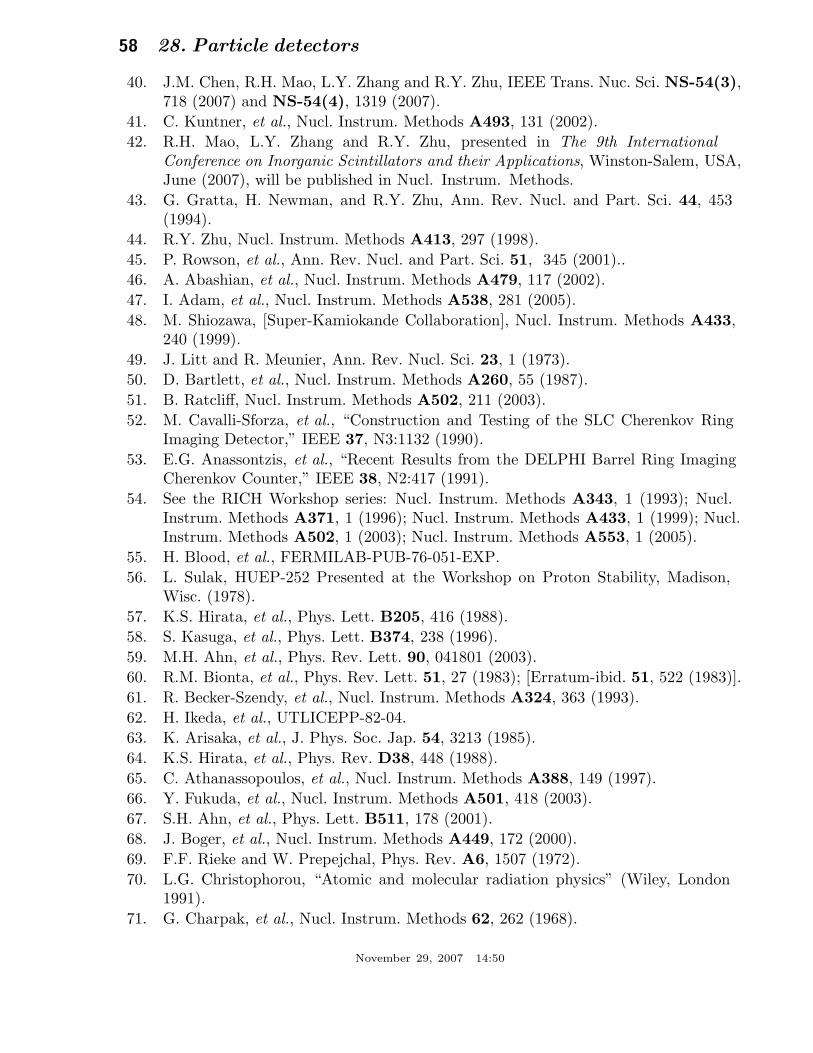
58 28. Particle detectors
40. J.M. Chen, R.H. Mao, L.Y. Zhang and R.Y. Zhu, IEEE Trans. Nuc. Sci. NS-54(3),718 (2007) and NS-54(4), 1319 (2007).
41. C. Kuntner, et al., Nucl. Instrum. Methods A493, 131 (2002).42. R.H. Mao, L.Y. Zhang and R.Y. Zhu, presented in The 9th International
Conference on Inorganic Scintillators and their Applications, Winston-Salem, USA,June (2007), will be published in Nucl. Instrum. Methods.
43. G. Gratta, H. Newman, and R.Y. Zhu, Ann. Rev. Nucl. and Part. Sci. 44, 453(1994).
44. R.Y. Zhu, Nucl. Instrum. Methods A413, 297 (1998).45. P. Rowson, et al., Ann. Rev. Nucl. and Part. Sci. 51, 345 (2001)..46. A. Abashian, et al., Nucl. Instrum. Methods A479, 117 (2002).47. I. Adam, et al., Nucl. Instrum. Methods A538, 281 (2005).48. M. Shiozawa, [Super-Kamiokande Collaboration], Nucl. Instrum. Methods A433,
240 (1999).49. J. Litt and R. Meunier, Ann. Rev. Nucl. Sci. 23, 1 (1973).50. D. Bartlett, et al., Nucl. Instrum. Methods A260, 55 (1987).51. B. Ratcliff, Nucl. Instrum. Methods A502, 211 (2003).52. M. Cavalli-Sforza, et al., “Construction and Testing of the SLC Cherenkov Ring
Imaging Detector,” IEEE 37, N3:1132 (1990).53. E.G. Anassontzis, et al., “Recent Results from the DELPHI Barrel Ring Imaging
Cherenkov Counter,” IEEE 38, N2:417 (1991).54. See the RICH Workshop series: Nucl. Instrum. Methods A343, 1 (1993); Nucl.
Instrum. Methods A371, 1 (1996); Nucl. Instrum. Methods A433, 1 (1999); Nucl.Instrum. Methods A502, 1 (2003); Nucl. Instrum. Methods A553, 1 (2005).
55. H. Blood, et al., FERMILAB-PUB-76-051-EXP.56. L. Sulak, HUEP-252 Presented at the Workshop on Proton Stability, Madison,
Wisc. (1978).57. K.S. Hirata, et al., Phys. Lett. B205, 416 (1988).58. S. Kasuga, et al., Phys. Lett. B374, 238 (1996).59. M.H. Ahn, et al., Phys. Rev. Lett. 90, 041801 (2003).60. R.M. Bionta, et al., Phys. Rev. Lett. 51, 27 (1983); [Erratum-ibid. 51, 522 (1983)].61. R. Becker-Szendy, et al., Nucl. Instrum. Methods A324, 363 (1993).62. H. Ikeda, et al., UTLICEPP-82-04.63. K. Arisaka, et al., J. Phys. Soc. Jap. 54, 3213 (1985).64. K.S. Hirata, et al., Phys. Rev. D38, 448 (1988).65. C. Athanassopoulos, et al., Nucl. Instrum. Methods A388, 149 (1997).66. Y. Fukuda, et al., Nucl. Instrum. Methods A501, 418 (2003).67. S.H. Ahn, et al., Phys. Lett. B511, 178 (2001).68. J. Boger, et al., Nucl. Instrum. Methods A449, 172 (2000).69. F.F. Rieke and W. Prepejchal, Phys. Rev. A6, 1507 (1972).70. L.G. Christophorou, “Atomic and molecular radiation physics” (Wiley, London
1991).71. G. Charpak, et al., Nucl. Instrum. Methods 62, 262 (1968).
November 29, 2007 14:50

28. Particle detectors 59
72. R. Veenhof, GARFIELD program: simulation of gaseous detectors, version 6.32,CERN Program Library Pool W999 (W5050).
73. As representative examples see: B. Adeva, et al., Nucl. Instrum. Methods A287,35 (1990).
74. As representative examples see: A. Alexander, et al., Nucl. Instrum. MethodsA276, 42 (1989).
75. As representative examples see: F. Bedeschi, et al., Nucl. Instrum. Methods A268,50 (1988);OPAL Collaboration: Nucl. Instrum. Methods A305, 275 (1991).
76. W. Blum and G. Rolandi, Particle Detection with Drift Chambers, Springer-Verlag(1994).
77. A. Peisert and F. Sauli, CERN-84-08 (Jul 1984).78. R. Bellazzini and A. M. Spezziga, Rivista del Nuovo Cimento 17, 1 (1994).79. A. Oed, Nucl. Instrum. Methods A263, 351 (1988).80. F. Sauli, Nucl. Instrum. Methods A386, 531 (1997).81. Y. Giomataris, et al., Nucl. Instrum. Methods A376, 29 (1996).82. F. Sauli and A. Sharma, Ann. Rev. Nucl. Part. Sci. 49, 341 (1999).83. Y. Bagaturia, et al., Nucl. Instrum. Methods A490, 223 (2002).84. F. Sauli, http://gdd.web.cern.ch/GDD/.85. J. Derre, et al., Nucl. Instrum. Methods A459, 523 (2001).86. I. Giomataris, et al., Nucl. Instrum. Methods A560, 405 (2006).87. R. Bellazzini, et al., Nucl. Instrum. Methods A535, 477 (2004).88. M. Campbell, et al., Nucl. Instrum. Methods A540, 295 (2005).89. A. Bamberger, et al., Nucl. Instrum. Methods A573, 361 (2007).90. M. Titov, physics/0403055; Proc. of the 42nd Workshop of the INFN
ELOISATRON Project, “Innovative Detectors For Super-Colliders,” Erice, Italy,Sept. 28–Oct. 4 (2003).
91. D.R. Nygren and J.N. Marx, “The Time Projection Chamber,” Phys. Today 31,46 (1978).
92. F. Sauli, Nucl. Instrum. Methods 386, 531 (1997).93. Y. Giomataris, Ph. Rebougeard, J.P. Robert and G. Charpak, Nucl. Instrum.
Methods 376, 29 (1996).94. X. Artru et al., Phys. Rev. D12, 1289 (1975).95. G.M. Garibian et al., Nucl. Instrum. Methods 125, 133 (1975).96. B. Dolgoshein, Nucl. Instrum. Methods A326, 434 (1993).97. G. Bassompierre et al., Nucl. Instrum. Methods 411, 63 (1998).98. A. Andronic, ALICE, Nucl. Instrum. Methods A522, 40 (2004).99. T. Akesson et al., ATLAS, Nucl. Instrum. Methods A412, 200 (1998).
100. M. Ambriola et al., PAMELA, Nucl. Instrum. Methods A522, 77 (2004).101. Ph. V. Doetinchem et al., AMS, Nucl. Instrum. Methods A558, 526 (2006).102. M. Brigida et al., Nucl. Instrum. Methods A572, 440 (2007).103. M.L. Cherry and G.L. Case, Nucl. Instrum. Methods A522, 73 (2004).104. D. Muller et al., Nucl. Instrum. Methods A522, 9 (2004).105. R. Santonico and R. Cardarelli, Nucl. Instrum. Methods A187, 377 (1981).
November 29, 2007 14:50

60 28. Particle detectors
106. V. V. Parkhomchuck, Yu. N. Pestov, & N. V. Petrovykh, Nucl. Instrum. Methods93, 269 (1971).
107. E. Cerron Zeballos et al., Nucl. Instrum. Methods A374, 132 (1996).108. V. Ammosov et al., Nucl. Instrum. Methods A578, 119 (2007).109. P. Fonte, IEEE. Trans. Nucl. Sci. 49, 881 (2002).110. M. Abbrescia et al., Nucl. Instrum. Methods A394, 13 (1997).111. F. Anulli et al., Nucl. Instrum. Methods A552, 276 (2005).112. H. Spieler, Semiconductor Detector Systems, Oxford Univ. Press, Oxford
(2005) ISBN 0-19-852784-5.113. F. Scholze, et al., Nucl. Instrum. Methods A439, 208 (2000).114. G. Lindstrom, et al., Nucl. Instrum. Methods A465, 60 (2001).115. C. Da Via, et al., Nucl. Instrum. Methods A509, 86 (2003).116. G. Kramberger, et al., Nucl. Instrum. Methods A481, 297 (2002).117. O. Krasel, et al., IEEE Trans. Nucl. Sci NS-51/6,3055(2004).118. G. Lindstrom, et al., Nucl. Instrum. Methods A426, 1 (1999).119. A. Holmes-Siedle and L. Adams, Handbook of Radiation Effects, 2nd ed., Oxford
2002, ISBN 0-19-850733-X, QC474.H59 2001.120. V. Radeka, IEEE Trans. Nucl. Sci. NS-15/3, 455 (1968);
V. Radeka, IEEE Trans. Nucl. Sci. NS-21, 51 (1974).121. F.S. Goulding, Nucl. Instrum. Methods 100, 493 (1972);
F.S. Goulding and D.A. Landis, IEEE Trans. Nucl. Sci. NS-29, 1125 (1982).122. W.R. Nelson, H. Hirayama, and D.W.O. Rogers, “The EGS4 Code System,”
SLAC-265, Stanford Linear Accelerator Center (Dec. 1985).123. R. Brun et al., GEANT3, CERN DD/EE/84-1 (1987).124. D. Hitlin et al., Nucl. Instrum. Methods 137, 225 (1976). See also W. J. Willis and
V. Radeka, Nucl. Instrum. Methods 120, 221 (1974), for a more detailed discussion.125. R. Wigmans, Calorimetry: Energy Measurement in Particle Physics, Clarendon,
Oxford (2000).126. ATLAS Collaboration, The ATLAS Liquid Argon Calorimeter Technical Design
Report, CERN/LHCC 96-41 (1996).127. CMS Collaboration, The CMS Electromagnetic Calorimeter Technical Design
Report, CERN/LHCC 97-33 (1997).128. C. Leroy and P.-G. Rancoita, Rep. Prog. Phys. 63, 505 (2000).129. D. Bintinger, in Proceedings of the Workshop on Calorimetry for the Supercollider,
Tuscaloosa, AL, March 13–17, 1989, edited by R. Donaldson and M.G.D. Gilchriese(World Scientific, Teaneck, NJ, 1989), p. 91;R.K. Bock, T. Hansl-Kozanecka, and T.P. Shah, Nucl. Instrum. Methods 186, 533(1981).
130. T.A. Gabriel, D.E. Groom, P.K. Job, N.V. Mokhov, and G.R. Stevenson, Nucl.Instrum. Methods A338, 336 (1994).
131. R. Wigmans, Nucl. Instrum. Methods A259, 389 (1987);R. Wigmans, Nucl. Instrum. Methods A265, 273 (1988).
132. N. Akchurian et al., Nucl. Instrum. Methods A408, 380 (1998).
November 29, 2007 14:50

28. Particle detectors 61
133. U. Behrens et al., Nucl. Instrum. Methods A289, 115 (1990);A. Bernstein et al., Nucl. Instrum. Methods A336, 23 (1993).
134. E. Bernardi et al., Nucl. Instrum. Methods A262, 229 (1987).135. S. Abachi et al., Nucl. Instrum. Methods A324, 53 (1993).136. F. Ariztizabal et al., Nucl. Instrum. Methods A349, 384 (1994).137. E. Shibamura et al., Nucl. Instrum. Methods 131, 249 (1975).138. T.G. Ryan and G.R. Freeman, J. Chem. Phys. 68, 5144 (1978).139. W.F. Schmidt, “Electron Migration in Liquids and Gases,” HMI B156 (1974).140. A.O. Allen, “Drift Mobilities and Conduction Band Energies of Excess Electrons in
Dielectric Liquids,” NSRDS-NBS-58 (1976).141. W. Walkowiak, Nucl. Instrum. Methods A449, 288 (2000).142. A. Yamamoto, Nucl. Instr. Meth. A453, 445 (2000).143. T. Taylor, Phys. Scr. 23, 459 (1980).144. A. Yamamoto, Nucl. Instr. Meth. A494, 255 (2003).145. R.L. Gluckstern, Nucl. Instrum. Methods 24, 381 (1963).146. V. Karimaki, Nucl. Instrum. Methods A410, 284 (1998).
November 29, 2007 14:50