functionalized rgo interlayers improve the fill factor and
TRANSCRIPT
materials
Article
Functionalized rGO Interlayers Improve the FillFactor and Current Density in PbS QDs-BasedSolar Cells
Anton A. Babaev *, Peter S. Parfenov, Dmitry A. Onishchuk, Aliaksei Dubavik,Sergei A. Cherevkov, Andrei V. Rybin, Mikhail A. Baranov, Alexander V. Baranov ,Aleksandr P. Litvin and Anatoly V. Fedorov
Center of Information optical technology, ITMO University, 197101 St. Petersburg, Russia;[email protected] (P.S.P.); [email protected] (D.A.O.); [email protected] (A.D.);[email protected] (S.A.C.); [email protected] (A.V.R.); [email protected] (M.A.B.);[email protected] (A.V.B.); [email protected] (A.P.L.); [email protected] (A.V.F.)* Correspondence: [email protected] or [email protected]
Received: 19 November 2019; Accepted: 11 December 2019; Published: 16 December 2019 �����������������
Abstract: Graphene-quantum dot nanocomposites attract significant attention for novel optoelectronicdevices, such as ultrafast photodetectors and third-generation solar cells. Combining the remarkableoptical properties of quantum dots (QDs) with the exceptional electrical properties of graphenederivatives opens a vast perspective for further growth in solar cell efficiency. Here, we applied(3-mercaptopropyl) trimethoxysilane functionalized reduced graphene oxide (f-rGO) to improvethe QDs-based solar cell active layer. The different strategies of f-rGO embedding are explored.When f-rGO interlayers are inserted between PbS QD layers, the solar cells demonstrate a highercurrent density and a better fill factor. A combined study of the morphological and electricalparameter s of the solar cells shows that the improved efficiency is associated with better layerhomogeneity, lower trap-state densities, higher charge carrier concentrations, and the blocking of theminor charge carriers.
Keywords: solar cells; reduced graphene oxide; quantum dots; impedance spectroscopy
1. Introduction
Many research groups are attempting to improve the efficiency and stability of lead sulfidecolloidal quantum dots (QDs) based solar cells [1–4]. In addition to being tunable throughout the NIRregion bandgap, low-cost solution processing and the capacity for multiple exciton generation makelead sulfide QDs a highly suitable material for solar cells. Currently, 12% power conversion efficiency(PCE) is the record for heterojunction PbS QDs-based solar cells [5]. However, it is still beyond thetheoretical limits of this material [6].
Defects in the active layer are among the main sources of charge carrier losses in solar cells. In solarcells based on QDs, the process of ligand replacement causes a rise in the defects in the active layer.Long ligands are replaced by short ones, which leads to the rearrangement of QDs and, as a result,to the formation of cracks and pinholes [7]. Nonetheless, the interdot spacing and layer homogeneityare crucial for layer conductivity [8]. In a number of works, graphene and its derivatives were appliedto improve the parameters of solar cells’ active layers [9–13], including morphology.
Graphene and its derivatives possess an excellent charge mobility and adjustable properties,which make them a promising material for photovoltaic applications [14]. Recently, BeatrizMartín-García et al., presented a noticeable technique [15] of reduced graphene oxide (rGO)
Materials 2019, 12, 4221; doi:10.3390/ma12244221 www.mdpi.com/journal/materials
Materials 2019, 12, 4221 2 of 10
functionalization by (3-Mercaptopropyl) trimethoxysilane (MPTS) for rGO-PbS QD linking thathas vast perspectives for device fabrication. Later, we showed that a preliminary colloidal-phase ligandexchange allows a higher efficiency of charge transfer between MPTS-bonded QDs and rGO to beachieved [16]. Additionally, it was shown that a thin layer of MPTS-bonded rGO-PbS deposited on topof a hole-transporting layer improves the stability of a solar cell [17].
Here, we show that MPTS-functionalized rGO (f-rGO) can be inserted into the active layer of a PbSQDs-based solar cell. The interlayers of f-rGO drastically boost the performance of a heterojunctionPbS QDs-based solar cell due to increased current density and improved fill factor (FF).
2. Materials and Methods
2.1. Materials
Precursors PbO (99.999%), hexamethyldisilathiane (TMS), zinc acetate dehydrate (99.99%Aldrich, Saint Louis, MO, USA), MAI (methylammonium iodide), EDT 1,2-ethanedithiol,TBAI (tetrabutylammonium iodide), and DMF (dimethylformamide anhydrous) were purchasedfrom Sigma-Aldrich (Saint Louis, MO, USA); acetonitrile from AppliChem (Darmstadt, Germany);octadecene (ODE) was obtained from Acros (Geel, Belgium); oleic acid (OlAc) from Fisher Chemicals(Waltham, MA, USA); EtOH (ethanol), MeOH (methanol), and chloroform were purchased fromVekton (St. Petersburg, Russia). Reduced graphene oxide (rGO) stabilized with poly (sodium4-styrenesulfonate) was purchased from Sigma-Aldrich as an aqueous solution and used as received.The 95% (3-Mercaptopropyl) trimethoxysilane (MPTS) was purchased from Sigma-Aldrich.
PbS QDs were synthesized using the hot-injection method described elsewhere [18,19]. Briefly,0.088 g of PbO was dissolved with 0.26 mL OlAc in 3.8 mL ODE at 90 ◦C under vacuum as a leadprecursor. The sulfur precursor was prepared by dissolving 70 µL TMS in 2 mL ODE. The sulfurprecursor was swiftly injected in the lead precursor at 85 ◦C, heated for 2 min, and cooled using awater-bath. The resulting QDs with a diameter of 3.5 nm were obtained by washing them with acetoneand centrifugation at 6000 RPM. The PL and absorption spectra of QDs are shown in SupplementaryMaterials Figure S1.
For the MAI phase ligand-exchange process, 1.5 mL of a 0.04 M MAI in 2:1 toluene-DMF solutionwas added at the rate of (3 µL·s−1) to 4 mL of the PbS QD solution with a concentration of 50 mg/mL,under gentle stirring. The resulting solution was kept under an inert atmosphere for 12 h to completethe exchange. Following this, MeOH was used to precipitate the solution, and finally, the solution wasredispersed in octane [20]. The solution in octane was ultrasonicated for 15 min and filtered through a0.22 µm syringe hydrophobic filter prior to use.
The method applied by Beatriz Martin-Garcia et al. [15] was used for rGO functionalization.Briefly, 10 mL of 0.5 mg/mL rGO dispersion in EtOH was sonicated for 30 min and refluxed at 60 ◦Cfor 15 h with 1.25 mL of MPTS. The resulting mixture was washed with EtOH by centrifugation andfinally dispersed in EtOH by sonication for 30 min. The solution was additionally sonicated for at least15 min just before use.
ZnO nanoparticles were synthesized according to the literature with some modifications [21].Thirteen millimoles of zinc acetate dehydrate was dissolved in 125 mL of methanol at 60 ◦C. Twenty-sixmillimoles of potassium hydroxide was dissolved in 65 mL of methanol. The potassium hydroxidesolution was slowly added to the zinc acetate solution and the solution was left stirring at 65 ◦C for 3 h.ZnO nanocrystals were extracted by centrifugation and then washed twice with methanol followed bycentrifugation. Finally, 10 mL of chloroform and 10 mL of methanol were added to the precipitates andthe solution was filtered with a 0.45 mm filter.
2.2. Device Fabrication
The devices were fabricated following the layer-by-layer spin-coating method according to [22].Fifty nanometers-thick ZnO layers were deposited on the clean pre-patterned ITO-coated glasses at
Materials 2019, 12, 4221 3 of 10
3000 rpm and annealed at 150 ◦C for 30 min. After cooling to room temperature, 6 layers of MAI-treatedQDs from 50 mg/mL octane solution were deposited at 2500 rpm on the ZnO film with a 2-stepligand-exchange procedure for each layer, using 15 mg/mL TBAI in methanol (MeOH) solution forexchange and acetonitrile (ACN) and hexane (HEX) for washing. Furthermore, 2 layers of OA-cappedPbS QDs were deposited from a HEX solution at 2500 rpm on the TBAI layers, with ligand exchangeusing 0.1% EDT in ACN as an exchange solution and ACN and HEX for washing. Finally, a 100 nm Auelectrode was deposited by magnetron plasma sputtering.
2.3. Measurements
The atomic force microscopy (AFM) measurements were provided using a Solver PRO-Mmicroscope (NT-MST, Moscow, Russia) in the semi-contact mode. The scanning electron microscopy(SEM) measurements were performed using a Merlin Zeiss electron microscope (Carl Zeiss, Oberkochen,Germany) in high vacuum mode at 10 kV accelerating voltages.
The light and dark J–V characteristics were measured by an Ossila Solar Cell I-V Test System.A solar simulator was used based on an OSRAM XBO-150W/1 xenon lamp (OSRAM, Munich, Germany).The light intensity adjusted was 100 mW/cm2. Capacitive and frequency characteristics were measuredby a Keysight E4980A LCR Meter (Keysight Technologies, Santa Rosa, CA, USA).
3. Results and Discussion
The conventional ITO-ZnO-PbS(TBAI)-PbS(EDT)-Au solar cell architecture, with MAI passivationQDs for the TBAI layer, was employed for our study. The preliminary colloidal-phase MAI of PbS QDssurface has been recently used to enhance the performance of PbS-based solar cells [20]. Additionally,we have recently shown that such a ligand exchange provides better charge transfer in rGO-PbS QDcomposites [16].
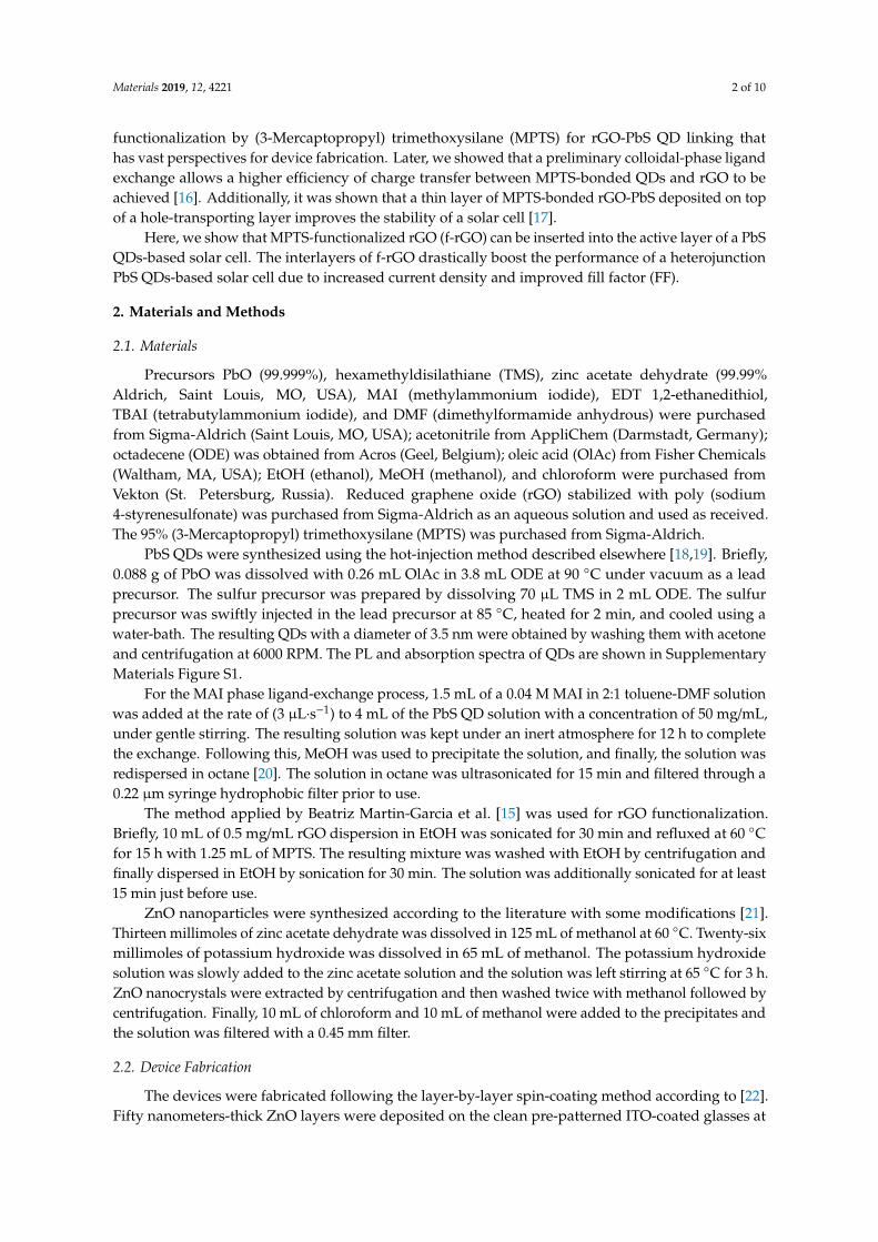
Devices with the three types of the active layer were explored, as shown in Figure 1a. For thereference device (Device 1), only MAI-treated QDs were employed for the active layer fabrication.For the f-rGO interlayers device (Device 2), the same conditions for Device 1 were used, but two dropsof the 0.05 mg/mL f-rGO in EtOH solution were additionally spin-coated on the interfaces betweenthe TBAI-treated PbS layers at 3000 rpm. For the device with an f-rGO-PbS hybrid in the active layer(Device 3), 0.5 mL of 50 mg/mL MAI-treated PbS colloidal solution in octane was mixed with 0.05 mLof 0.5 mg/mL f-rGO in EtOH solution by stirring for 30 min at 2000 rpm. These hybrid inks wereemployed instead of QD inks for the fabrication of six TBAI layers in Device 3 with the same depositionand ligand-exchange conditions as for Device 1. The PbS(EDT) hole transport layer remained the samefor all the devices. The light parameters of the devices are represented in Table 1.
Table 1. The fill factor (FF), JSC, and VOC values of the reference, functionalized reduced grapheneoxide (f-rGO) interlayers, and f-rGO mix devices.
Device FF (%) JSC (mA·cm−2) VOC (V) PCE (%)
Reference (1) 48.4 ± 3.5 13.5 ± 1.2 0.57 ± 0.005 3.5 ± 0.4Interlayers (2) 54.2 ± 0.3 14.2 ± 1.3 0.55 ± 0.005 4.2 ± 0.35
Hybrid (3) 42.6 ± 6 10.8 ± 0.2 0.54 ± 0.018 2.5 ± 0.4
Figure 1b presents the J–V curves obtained for the three types of devices. As seen, the devices withf-rGO interlayers possess better current, while the f-rGO mixture device suffers current quenching,and both devices exhibit slight VOC reduction. Moreover, Device 2 has a significant FF improvement.The FF, short circuit current density (JSC) and open circuit voltage (VOC) values are given in Table S1.The AFM, capacitance–voltage (C–V), and capacitance–frequency (C–F) measurements were performedto reveal the nature of the changes.
Materials 2019, 12, 4221 4 of 10Materials 2020, 13, x FOR PEER REVIEW 4 of 11
Figure 1. (a) Schematic illustration of the reference (Device 1), interlayers (Device 2), and hybrid structures (Device 3); (b) J–V curves of the devices.
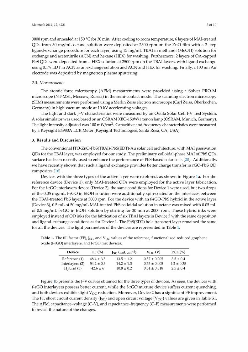
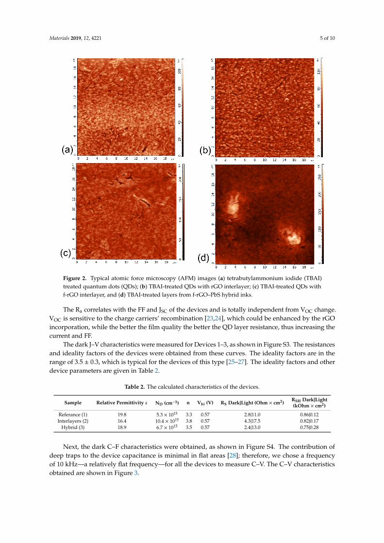
The AFM measurements were performed to examine the influence of the rGO on the film quality. The following samples were compared:
(1) 2-layer sample of TBAI-treated QDs; (2) 2-layer sample of TBAI-treated QDs with rGO interlayer; (3) 2-layer sample of TBAI-treated QDs with f-rGO interlayer; (4) 2-layer sample of TBAI-treated layers from f-rGO-PbS hybrid inks.
The samples obtained were measured on 20 × 20 μm of 10 randomly selected areas on each sample, and average roughness (Ra) data were calculated by NT-MDT NOVA image analysis software and averaged on the measured points. The examples of AFM images are shown in Figure 2, and the average roughness data are given in Table S2. Additionally, the listed structures were studied using SEM (Figure S2). The lower average roughness indicates a lower amount of cracks and pinholes. From the data, it follows that the f-rGO interlayers help minimize the quantity of the defects in the planar PbS layer-by-layer film, while using f-rGO–PbS hybrid inks results in huge aggregates
Figure 1. (a) Schematic illustration of the reference (Device 1), interlayers (Device 2), and hybridstructures (Device 3); (b) J–V curves of the devices.
The AFM measurements were performed to examine the influence of the rGO on the film quality.The following samples were compared:
(1) 2-layer sample of TBAI-treated QDs;(2) 2-layer sample of TBAI-treated QDs with rGO interlayer;(3) 2-layer sample of TBAI-treated QDs with f-rGO interlayer;(4) 2-layer sample of TBAI-treated layers from f-rGO-PbS hybrid inks.
The samples obtained were measured on 20 × 20 µm of 10 randomly selected areas on eachsample, and average roughness (Ra) data were calculated by NT-MDT NOVA image analysis softwareand averaged on the measured points. The examples of AFM images are shown in Figure 2, and theaverage roughness data are given in Table S2. Additionally, the listed structures were studied usingSEM (Figure S2). The lower average roughness indicates a lower amount of cracks and pinholes.From the data, it follows that the f-rGO interlayers help minimize the quantity of the defects in theplanar PbS layer-by-layer film, while using f-rGO–PbS hybrid inks results in huge aggregates in thefilm. In contrast, the non-functionalized rGO layer corrupts the film quality, which confirms that theMPTS linker attached to rGO plays a key role in the improvement of the films’ morphology.
Materials 2019, 12, 4221 5 of 10
Materials 2020, 13, x FOR PEER REVIEW 5 of 11 in the film. In contrast, the non-functionalized rGO layer corrupts the film quality, which confirms that the MPTS linker attached to rGO plays a key role in the improvement of the films’ morphology.
Figure 2. Typical atomic force microscopy (AFM) images (a) tetrabutylammonium iodide (TBAI) treated quantum dots (QDs); (b) TBAI-treated QDs with rGO interlayer; (c) TBAI-treated QDs with f-rGO interlayer, and (d) TBAI-treated layers from f-rGO–PbS hybrid inks.
The Ra correlates with the FF and JSC of the devices and is totally independent from VOC change. VOC is sensitive to the charge carriers’ recombination [23,24], which could be enhanced by the rGO incorporation, while the better the film quality the better the QD layer resistance, thus increasing the current and FF.
The dark J–V characteristics were measured for Devices 1–3, as shown in Figure S3. The resistances and ideality factors of the devices were obtained from these curves. The ideality factors are in the range of 3.5 ± 0.3, which is typical for the devices of this type [25–27]. The ideality factors and other device parameters are given in Table 2.
Table 2. The calculated characteristics of the devices.
Sample Relative
Permittivity ε
ND (cm−3) n Vbi (V) RS Dark|Light (Ohm × cm2)
RSH Dark|Light (kOhm × cm2)
Referance (1) 19.8 5.3 × 10¹⁵ 3.3 0.57 2.8|11.0 0.86|0.12 Interlayers (2) 16.4 10.4 × 10¹⁵ 3.8 0.57 4.3|17.5 0.82|0.17
Hybrid (3) 18.9 6.7 × 10¹⁵ 3.5 0.57 2.4|13.0 0.75|0.28
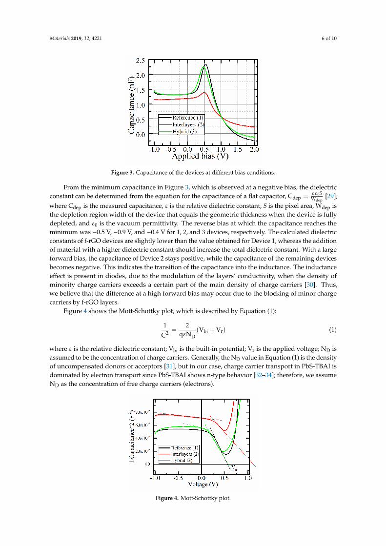
Next, the dark C–F characteristics were obtained, as shown in Figure S4. The contribution of deep traps to the device capacitance is minimal in flat areas [28]; therefore, we chose a frequency of 10 kHz—a relatively flat frequency—for all the devices to measure C–V. The C–V characteristics obtained are shown in Figure 3.
Figure 2. Typical atomic force microscopy (AFM) images (a) tetrabutylammonium iodide (TBAI)treated quantum dots (QDs); (b) TBAI-treated QDs with rGO interlayer; (c) TBAI-treated QDs withf-rGO interlayer, and (d) TBAI-treated layers from f-rGO–PbS hybrid inks.
The Ra correlates with the FF and JSC of the devices and is totally independent from VOC change.VOC is sensitive to the charge carriers’ recombination [23,24], which could be enhanced by the rGOincorporation, while the better the film quality the better the QD layer resistance, thus increasing thecurrent and FF.
The dark J–V characteristics were measured for Devices 1–3, as shown in Figure S3. The resistancesand ideality factors of the devices were obtained from these curves. The ideality factors are in therange of 3.5 ± 0.3, which is typical for the devices of this type [25–27]. The ideality factors and otherdevice parameters are given in Table 2.
Table 2. The calculated characteristics of the devices.
Sample Relative Permittivity ε ND (cm−3) n Vbi (V) RS Dark|Light (Ohm × cm2)RSH Dark|Light(kOhm × cm2)
Referance (1) 19.8 5.3 × 10¹⁵ 3.3 0.57 2.8|11.0 0.86|0.12Interlayers (2) 16.4 10.4 × 10¹⁵ 3.8 0.57 4.3|17.5 0.82|0.17
Hybrid (3) 18.9 6.7 × 10¹⁵ 3.5 0.57 2.4|13.0 0.75|0.28
Next, the dark C–F characteristics were obtained, as shown in Figure S4. The contribution ofdeep traps to the device capacitance is minimal in flat areas [28]; therefore, we chose a frequencyof 10 kHz—a relatively flat frequency—for all the devices to measure C–V. The C–V characteristicsobtained are shown in Figure 3.
Materials 2019, 12, 4221 6 of 10Materials 2020, 13, x FOR PEER REVIEW 6 of 11
Figure 3. Capacitance of the devices at different bias conditions.
From the minimum capacitance in Figure 3, which is observed at a negative bias, the dielectric constant can be determined from the equation for the capacitance of a flat capacitor, C = [29],
where Cdep is the measured capacitance, ε is the relative dielectric constant, S is the pixel area, Wdep is the depletion region width of the device that equals the geometric thickness when the device is fully depleted, and ε0 is the vacuum permittivity. The reverse bias at which the capacitance reaches the minimum was −0.5 V, −0.9 V, and −0.4 V for 1, 2, and 3 devices, respectively. The calculated dielectric constants of f-rGO devices are slightly lower than the value obtained for Device 1, whereas the addition of material with a higher dielectric constant should increase the total dielectric constant. With a large forward bias, the capacitance of Device 2 stays positive, while the capacitance of the remaining devices becomes negative. This indicates the transition of the capacitance into the inductance. The inductance effect is present in diodes, due to the modulation of the layers’ conductivity, when the density of minority charge carriers exceeds a certain part of the main density of charge carriers [30]. Thus, we believe that the difference at a high forward bias may occur due to the blocking of minor charge carriers by f-rGO layers.
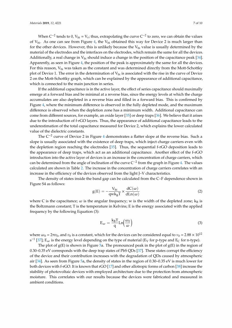
Figure 4 shows the Mott-Schottky plot, which is described by Equation (1): 1С = 2qεN (V + V ) (1)
where ε is the relative dielectric constant; Vbi is the built-in potential; Vr is the applied voltage; ND is assumed to be the concentration of charge carriers. Generally, the ND value in Equation (1) is the density of uncompensated donors or acceptors [31], but in our case, charge carrier transport in PbS-TBAI is dominated by electron transport since PbS-TBAI shows n-type behavior[32–34]; therefore, we assume ND as the concentration of free charge carriers (electrons).
Figure 3. Capacitance of the devices at different bias conditions.
From the minimum capacitance in Figure 3, which is observed at a negative bias, the dielectricconstant can be determined from the equation for the capacitance of a flat capacitor, Cdep = εε0S
Wdep[29],
where Cdep is the measured capacitance, ε is the relative dielectric constant, S is the pixel area, Wdep isthe depletion region width of the device that equals the geometric thickness when the device is fullydepleted, and ε0 is the vacuum permittivity. The reverse bias at which the capacitance reaches theminimum was −0.5 V, −0.9 V, and −0.4 V for 1, 2, and 3 devices, respectively. The calculated dielectricconstants of f-rGO devices are slightly lower than the value obtained for Device 1, whereas the additionof material with a higher dielectric constant should increase the total dielectric constant. With a largeforward bias, the capacitance of Device 2 stays positive, while the capacitance of the remaining devicesbecomes negative. This indicates the transition of the capacitance into the inductance. The inductanceeffect is present in diodes, due to the modulation of the layers’ conductivity, when the density ofminority charge carriers exceeds a certain part of the main density of charge carriers [30]. Thus,we believe that the difference at a high forward bias may occur due to the blocking of minor chargecarriers by f-rGO layers.
Figure 4 shows the Mott-Schottky plot, which is described by Equation (1):
1
C2 =2
qεND(Vbi + Vr) (1)
where ε is the relative dielectric constant; Vbi is the built-in potential; Vr is the applied voltage; ND isassumed to be the concentration of charge carriers. Generally, the ND value in Equation (1) is the densityof uncompensated donors or acceptors [31], but in our case, charge carrier transport in PbS-TBAI isdominated by electron transport since PbS-TBAI shows n-type behavior [32–34]; therefore, we assumeND as the concentration of free charge carriers (electrons).
Materials 2020, 13, x FOR PEER REVIEW 7 of 11
Figure 4. Mott-Schottky plot.
When C−2 tends to 0, Vbi = Vr; thus, extrapolating the curve C−2 to zero, we can obtain the values of Vbi. As one can see from Figure 4, the Vbi obtained this way for Device 2 is much larger than for the other devices. However, this is unlikely because the Vbi value is usually determined by the material of the electrodes and the interfaces on the electrodes, which remain the same for all the devices. Additionally, a real change in Vbi should induce a change in the position of the capacitance peak [34]. Apparently, as seen in Figure 4, the position of the peak is approximately the same for all the devices. For this reason, Vbi was taken as the constant and was determined directly from the Mott-Schottky plot of Device 1. The error in the determination of Vbi is associated with the rise in the curve of Device 2 on the Mott-Schottky graph, which can be explained by the appearance of additional capacitance, which is connected to the main junction in series.
If the additional capacitance is in the active layer, the effect of series capacitance should maximally emerge at a forward bias and be minimal at a reverse bias, since the energy levels at which the charge accumulates are also depleted in a reverse bias and filled in a forward bias. This is confirmed by Figure 4, where the minimum difference is observed in the fully depleted mode, and the maximum difference is observed when the depletion zone has a minimum width. Additional capacitance can come from different sources, for example, an oxide layer [35] or deep traps [36]. We believe that it arises due to the introduction of f-rGO layers. Thus, the appearance of additional capacitance leads to the underestimation of the total capacitance measured for Device 2, which explains the lower calculated value of the dielectric constants.
The C−2 curve of Device 2 in Figure 4 demonstrates a flatter slope at the reverse bias. Such a slope is usually associated with the existence of deep traps, which inject charge carriers even with the depletion region reaching the electrodes [35]. Thus, the sequential f-rGO deposition leads to the appearance of deep traps, which act as an additional capacitance. Another effect of the f-rGO introduction into the active layer of devices is an increase in the concentration of charge carriers, which can be determined from the angle of inclination of the curve C−2 from the graph in Figure 4. The values calculated are shown in Table 2. The increase in the concentration of charge carriers correlates with an increase in the efficiency of the devices observed from the light J–V characteristics.
The density of states inside the band gap can be calculated from the С–F dependence shown in Figure S4 as follows: g(E) = − Vqwk T × dC(ω)dLn(ω) (2)
where C is the capacitance; ω is the angular frequency; w is the width of the depleted zone; kB is the Boltzmann constant; T is the temperature in Kelvins; E is the energy associated with the applied frequency by the following Equation (3):
Figure 4. Mott-Schottky plot.
Materials 2019, 12, 4221 7 of 10
When C−2 tends to 0, Vbi = Vr; thus, extrapolating the curve C−2 to zero, we can obtain the valuesof Vbi. As one can see from Figure 4, the Vbi obtained this way for Device 2 is much larger thanfor the other devices. However, this is unlikely because the Vbi value is usually determined by thematerial of the electrodes and the interfaces on the electrodes, which remain the same for all the devices.Additionally, a real change in Vbi should induce a change in the position of the capacitance peak [34].Apparently, as seen in Figure 4, the position of the peak is approximately the same for all the devices.For this reason, Vbi was taken as the constant and was determined directly from the Mott-Schottkyplot of Device 1. The error in the determination of Vbi is associated with the rise in the curve of Device2 on the Mott-Schottky graph, which can be explained by the appearance of additional capacitance,which is connected to the main junction in series.
If the additional capacitance is in the active layer, the effect of series capacitance should maximallyemerge at a forward bias and be minimal at a reverse bias, since the energy levels at which the chargeaccumulates are also depleted in a reverse bias and filled in a forward bias. This is confirmed byFigure 4, where the minimum difference is observed in the fully depleted mode, and the maximumdifference is observed when the depletion zone has a minimum width. Additional capacitance cancome from different sources, for example, an oxide layer [35] or deep traps [36]. We believe that it arisesdue to the introduction of f-rGO layers. Thus, the appearance of additional capacitance leads to theunderestimation of the total capacitance measured for Device 2, which explains the lower calculatedvalue of the dielectric constants.
The C−2 curve of Device 2 in Figure 4 demonstrates a flatter slope at the reverse bias. Such aslope is usually associated with the existence of deep traps, which inject charge carriers even withthe depletion region reaching the electrodes [35]. Thus, the sequential f-rGO deposition leads tothe appearance of deep traps, which act as an additional capacitance. Another effect of the f-rGOintroduction into the active layer of devices is an increase in the concentration of charge carriers, whichcan be determined from the angle of inclination of the curve C−2 from the graph in Figure 4. The valuescalculated are shown in Table 2. The increase in the concentration of charge carriers correlates with anincrease in the efficiency of the devices observed from the light J–V characteristics.
The density of states inside the band gap can be calculated from the C–F dependence shown inFigure S4 as follows:
g(E) = −Vbi
qwkBT×
dC(ω)
dLn(ω)(2)
where C is the capacitance; ω is the angular frequency; w is the width of the depleted zone; kB isthe Boltzmann constant; T is the temperature in Kelvins; E is the energy associated with the appliedfrequency by the following Equation (3):
Eω =kBT
qLn(ω0
ω
)(3)
whereω0 = 2πv0, and v0 is a constant, which for the devices can be considered equal to ν0 = 2.88 × 10¹²
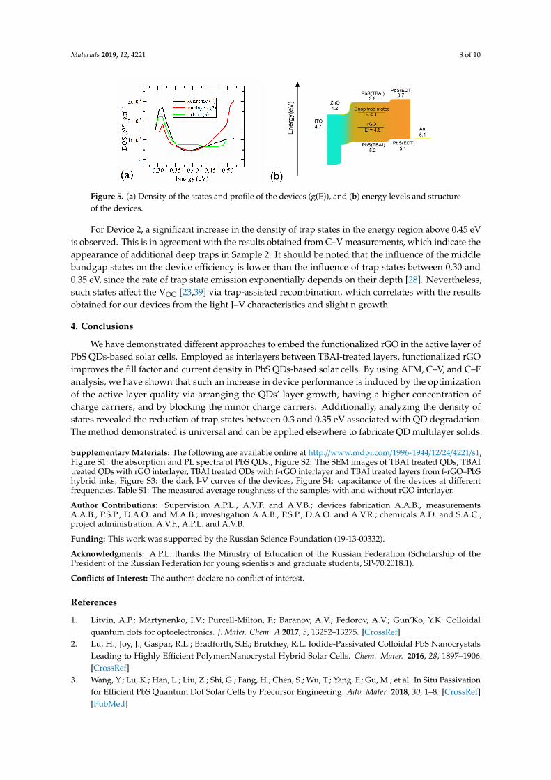
s−1 [37]; Eω is the energy level depending on the type of material (EV for p-type and EC for n-type).The plot of g(E) is shown in Figure 5a. The pronounced peak in the plot of g(E) in the region of
0.30–0.35 eV corresponds with the deep trap states of PbS QDs [37]. These states corrupt the efficiencyof the device and their contribution increases with the degradation of QDs caused by atmosphericair [34]. As seen from Figure 5a, the density of states in the region of 0.30–0.35 eV is much lower forboth devices with f-rGO. It is known that rGO [17] and other allotropic forms of carbon [38] increase thestability of photovoltaic devices with employed architecture due to the protection from atmosphericmoisture. This correlates with our results because the devices were fabricated and measured inambient conditions.
Materials 2019, 12, 4221 8 of 10
Materials 2020, 13, x FOR PEER REVIEW 8 of 11
E = k Tq Ln ωω (3)
where ω0 = 2πv0, and v0 is a constant, which for the devices can be considered equal to ν0 = 2.88 × 10¹² s−1 [37]; Eω is the energy level depending on the type of material (EV for p-type and EC for n-type).
The plot of g(E) is shown in Figure 5a. The pronounced peak in the plot of g(E) in the region of 0.30–0.35 eV corresponds with the deep trap states of PbS QDs [37]. These states corrupt the efficiency of the device and their contribution increases with the degradation of QDs caused by atmospheric air [34]. As seen from Figure 5a, the density of states in the region of 0.30–0.35 eV is much lower for both devices with f-rGO. It is known that rGO [17] and other allotropic forms of carbon [38] increase the stability of photovoltaic devices with employed architecture due to the protection from atmospheric moisture. This correlates with our results because the devices were fabricated and measured in ambient conditions.
Figure 5. (a) Density of the states and profile of the devices (g(E)), and (b) energy levels and structure of the devices.
For Device 2, a significant increase in the density of trap states in the energy region above 0.45 eV is observed. This is in agreement with the results obtained from C–V measurements, which indicate the appearance of additional deep traps in Sample 2. It should be noted that the influence of the middle bandgap states on the device efficiency is lower than the influence of trap states between 0.30 and 0.35 eV, since the rate of trap state emission exponentially depends on their depth [28]. Nevertheless, such states affect the VOC [23,39] via trap-assisted recombination, which correlates with the results obtained for our devices from the light J–V characteristics and slight n growth.
4. Conclusions
We have demonstrated different approaches to embed the functionalized rGO in the active layer of PbS QDs-based solar cells. Employed as interlayers between TBAI-treated layers, functionalized rGO improves the fill factor and current density in PbS QDs-based solar cells. By using AFM, C–V, and C–F analysis, we have shown that such an increase in device performance is induced by the optimization of the active layer quality via arranging the QDs’ layer growth, having a higher concentration of charge carriers, and by blocking the minor charge carriers. Additionally, analyzing the density of states revealed the reduction of trap states between 0.3 and 0.35 eV associated with QD degradation. The method demonstrated is universal and can be applied elsewhere to fabricate QD multilayer solids.
Supplementary Materials: The following are available online at www.mdpi.com/xxx/s1, Figure S1: the absorption and PL spectra of PbS QDs., Figure S2: The SEM images of TBAI treated QDs, TBAI treated QDs with rGO interlayer, TBAI treated QDs with f-rGO interlayer and TBAI treated layers from f-rGO–PbS hybrid inks, Figure S3: the dark I-V curves of the devices, Figure S4: capacitance of the devices at different frequencies, Table S1: The measured average roughness of the samples with and without rGO interlayer.
Figure 5. (a) Density of the states and profile of the devices (g(E)), and (b) energy levels and structureof the devices.
For Device 2, a significant increase in the density of trap states in the energy region above 0.45 eVis observed. This is in agreement with the results obtained from C–V measurements, which indicate theappearance of additional deep traps in Sample 2. It should be noted that the influence of the middlebandgap states on the device efficiency is lower than the influence of trap states between 0.30 and0.35 eV, since the rate of trap state emission exponentially depends on their depth [28]. Nevertheless,such states affect the VOC [23,39] via trap-assisted recombination, which correlates with the resultsobtained for our devices from the light J–V characteristics and slight n growth.
4. Conclusions
We have demonstrated different approaches to embed the functionalized rGO in the active layer ofPbS QDs-based solar cells. Employed as interlayers between TBAI-treated layers, functionalized rGOimproves the fill factor and current density in PbS QDs-based solar cells. By using AFM, C–V, and C–Fanalysis, we have shown that such an increase in device performance is induced by the optimizationof the active layer quality via arranging the QDs’ layer growth, having a higher concentration ofcharge carriers, and by blocking the minor charge carriers. Additionally, analyzing the density ofstates revealed the reduction of trap states between 0.3 and 0.35 eV associated with QD degradation.The method demonstrated is universal and can be applied elsewhere to fabricate QD multilayer solids.
Supplementary Materials: The following are available online at http://www.mdpi.com/1996-1944/12/24/4221/s1,Figure S1: the absorption and PL spectra of PbS QDs., Figure S2: The SEM images of TBAI treated QDs, TBAItreated QDs with rGO interlayer, TBAI treated QDs with f-rGO interlayer and TBAI treated layers from f-rGO–PbShybrid inks, Figure S3: the dark I-V curves of the devices, Figure S4: capacitance of the devices at differentfrequencies, Table S1: The measured average roughness of the samples with and without rGO interlayer.
Author Contributions: Supervision A.P.L., A.V.F. and A.V.B.; devices fabrication A.A.B., measurementsA.A.B., P.S.P., D.A.O. and M.A.B.; investigation A.A.B., P.S.P., D.A.O. and A.V.R.; chemicals A.D. and S.A.C.;project administration, A.V.F., A.P.L. and A.V.B.
Funding: This work was supported by the Russian Science Foundation (19-13-00332).
Acknowledgments: A.P.L. thanks the Ministry of Education of the Russian Federation (Scholarship of thePresident of the Russian Federation for young scientists and graduate students, SP-70.2018.1).
Conflicts of Interest: The authors declare no conflict of interest.
References
1. Litvin, A.P.; Martynenko, I.V.; Purcell-Milton, F.; Baranov, A.V.; Fedorov, A.V.; Gun’Ko, Y.K. Colloidalquantum dots for optoelectronics. J. Mater. Chem. A 2017, 5, 13252–13275. [CrossRef]
2. Lu, H.; Joy, J.; Gaspar, R.L.; Bradforth, S.E.; Brutchey, R.L. Iodide-Passivated Colloidal PbS NanocrystalsLeading to Highly Efficient Polymer:Nanocrystal Hybrid Solar Cells. Chem. Mater. 2016, 28, 1897–1906.[CrossRef]
3. Wang, Y.; Lu, K.; Han, L.; Liu, Z.; Shi, G.; Fang, H.; Chen, S.; Wu, T.; Yang, F.; Gu, M.; et al. In Situ Passivationfor Efficient PbS Quantum Dot Solar Cells by Precursor Engineering. Adv. Mater. 2018, 30, 1–8. [CrossRef][PubMed]

Materials 2019, 12, 4221 9 of 10
4. Carey, G.H.; Abdelhady, A.L.; Ning, Z.; Thon, S.M.; Bakr, O.M.; Sargent, E.H. Colloidal Quantum Dot SolarCells. Chem. Rev. 2015, 115, 12732–12763. [CrossRef]
5. Xu, J.; Voznyy, O.; Liu, M.; Kirmani, A.R.; Walters, G.; Munir, R.; Abdelsamie, M.; Proppe, A.H.; Sarkar, A.;García De Arquer, F.P.; et al. 2D matrix engineering for homogeneous quantum dot coupling in photovoltaicsolids. Nat. Nanotechnol. 2018, 13, 456–462. [CrossRef]
6. Malgras, V.; Nattestad, A.; Kim, J.H.; Dou, S.X.; Yamauchi, Y. Understanding chemically processed solar cellsbased on quantum dots. Sci. Technol. Adv. Mater. 2017, 18, 334–350. [CrossRef]
7. Liu, M.; Voznyy, O.; Sabatini, R.; García De Arquer, F.P.; Munir, R.; Balawi, A.H.; Lan, X.; Fan, F.; Walters, G.;Kirmani, A.R.; et al. Hybrid organic-inorganic inks flatten the energy landscape in colloidal quantum dotsolids. Nat. Mater. 2017, 16, 258–263. [CrossRef]
8. Chistyakov, A.A.; Zvaigzne, M.A.; Nikitenko, V.R.; Tameev, A.R.; Martynov, I.L.; Prezhdo, O.V. OptoelectronicProperties of Semiconductor Quantum Dot Solids for Photovoltaic Applications. J. Phys. Chem. Lett. 2017,8, 4129–4139. [CrossRef]
9. Hadadian, M.; Correa-Baena, J.P.; Goharshadi, E.K.; Ummadisingu, A.; Seo, J.Y.; Luo, J.; Gholipour, S.;Zakeeruddin, S.M.; Saliba, M.; Abate, A.; et al. Enhancing Efficiency of Perovskite Solar Cells via N-dopedGraphene: Crystal Modification and Surface Passivation. Adv. Mater. 2016, 28, 8681–8686. [CrossRef]
10. Kim, B.-S.; Neo, D.C.J.; Hou, B.; Park, J.B.; Cho, Y.; Zhang, N.; Hong, J.; Pak, S.; Lee, S.; Sohn, J.I.; et al. HighPerformance PbS Quantum Dot/Graphene Hybrid Solar Cell with Efficient Charge Extraction. ACS Appl.Mater. Interfaces 2016, 8, 13902–13908. [CrossRef]
11. Jun, G.H.; Jin, S.H.; Lee, B.; Kim, B.H.; Chae, W.S.; Hong, S.H.; Jeon, S. Enhanced conduction andcharge-selectivity by N-doped graphene flakes in the active layer of bulk-heterojunction organic solar cells.Energy Environ. Sci. 2013, 6, 3000–3006. [CrossRef]
12. Hu, L.; Li, D.B.; Gao, L.; Tan, H.; Chen, C.; Li, K.; Li, M.; Han, J.B.; Song, H.; Liu, H.; et al. Graphene DopingImproved Device Performance of ZnMgO/PbS Colloidal Quantum Dot Photovoltaics. Adv. Funct. Mater.2016, 26, 1899–1907. [CrossRef]
13. Mahmoudi, T.; Wang, Y.; Hahn, Y.B. Graphene and its derivatives for solar cells application. Nano Energy2018, 47, 51–65. [CrossRef]
14. Yin, Z.; Zhu, J.; He, Q.; Cao, X.; Tan, C.; Chen, H.; Yan, Q.; Zhang, H. Graphene-Based materials for solar cellapplications. Adv. Energy Mater. 2014, 4, 1–19. [CrossRef]
15. Martín-García, B.; Polovitsyn, A.; Prato, M.; Moreels, I. Efficient charge transfer in solution-processed PbSquantum dot-reduced graphene oxide hybrid materials. J. Mater. Chem. C 2015, 3, 7088–7095. [CrossRef]
16. Babaev, A.; Dubavik, A.; Cherevkov, S.; Parfenov, P.; Ushakova, E.; Baranov, M.; Nabiev, I.; Baranov, A.;Litvin, A. Optical properties of PBS-GO and PBS-RGO system for solar cells fabrication. In Proceedings of theNANOCON 2018–10th Anniversary International Conference on Nanomaterials–Research and Application,Brno, Czech Republic, 17–19 October 2018; pp. 24–29.
17. Martín-García, B.; Bi, Y.; Prato, M.; Spirito, D.; Krahne, R.; Konstantatos, G.; Moreels, I. Reduction of moisturesensitivity of PbS quantum dot solar cells by incorporation of reduced graphene oxide. Sol. Energy Mater.Sol. Cells 2018, 183, 1–7. [CrossRef]
18. Hines, M.A.; Scholes, G.D. Colloidal PbS Nanocrystals with Size-Tunable Near-Infrared Emission:Observation of Post-Synthesis Self-Narrowing of the Particle Size Distribution. Adv. Mater. 2003,15, 1844–1849. [CrossRef]
19. Ushakova, E.V.; Litvin, A.P.; Parfenov, P.S.; Fedorov, A.V.; Artemyev, M.; Prudnikau, A.V.; Rukhlenko, I.D.;Baranov, A.V. Anomalous size-dependent decay of low-energy luminescence from PbS quantum dots incolloidal solution. ACS Nano 2012, 6, 8913–8921. [CrossRef]
20. Lan, X.; Voznyy, O.; García De Arquer, F.P.; Liu, M.; Xu, J.; Proppe, A.H.; Walters, G.; Fan, F.; Tan, H.; Liu, M.;et al. 10.6% Certified Colloidal Quantum Dot Solar Cells Via Solvent-Polarity-Engineered Halide Passivation.Nano Lett. 2016, 16, 4630–4634. [CrossRef]
21. Shi, G.; Wang, Y.; Liu, Z.; Han, L.; Liu, J.; Wang, Y.; Lu, K.; Chen, S.; Ling, X.; Li, Y.; et al. Stable and HighlyEfficient PbS Quantum Dot Tandem Solar Cells Employing a Rationally Designed Recombination Layer.Adv. Energy Mater. 2017, 7, 1602667. [CrossRef]
22. Lu, K.; Wang, Y.; Liu, Z.; Han, L.; Shi, G.; Fang, H.; Chen, J.; Ye, X.; Chen, S.; Yang, F.; et al. High-Efficiency PbSQuantum-Dot Solar Cells with Greatly Simplified Fabrication Processing via “Solvent-Curing”. Adv. Mater.2018, 30, 1–9. [CrossRef] [PubMed]
Materials 2019, 12, 4221 10 of 10
23. Chuang, C.H.M.; Maurano, A.; Brandt, R.E.; Hwang, G.W.; Jean, J.; Buonassisi, T.; Bulovic, V.; Bawendi, M.G.Open-circuit voltage deficit, radiative sub-bandgap states, and prospects in quantum dot solar cells. Nano Lett.2015, 15, 3286–3294. [CrossRef]
24. Karki, A.; Vollbrecht, J.; Dixon, A.L.; Schopp, N.; Schrock, M.; Reddy, G.N.M.; Nguyen, T. Understandingthe High Performance of over 15% Efficiency in Single-Junction Bulk Heterojunction Organic Solar Cells.Adv. Mater. 2019, 31, 1903868. [CrossRef] [PubMed]
25. Gao, W.; Zhai, G.; Zhang, C.; Shao, Z.; Zheng, L.; Zhang, Y.; Yang, Y.; Li, X.; Liu, X.; Xu, B. Towardsunderstanding the initial performance improvement of PbS quantum dot solar cells upon short-term airexposure. RSC Adv. 2018, 8, 15149–15157. [CrossRef]
26. Pradhan, S.; Stavrinadis, A.; Gupta, S.; Christodoulou, S.; Konstantatos, G. Breaking the Open-Circuit VoltageDeficit Floor in PbS Quantum Dot Solar Cells through Synergistic Ligand and Architecture Engineering.ACS Energy Lett. 2017, 2, 1444–1449. [CrossRef]
27. Yoon, W.; Boercker, J.E.; Lumb, M.P.; Placencia, D.; Foos, E.E.; Tischler, J.G. Enhanced open-circuit voltage ofPbS nanocrystal quantum dot solar cells. Sci. Rep. 2013, 3, 2225. [CrossRef]
28. Esfahani, M.S. Device Physics of Organic and Perovskite Solar Cells; Iowa State University: Ames, IA, USA, 2015;ISBN 9789403404615.
29. Speirs, M.J.; Dirin, D.N.; Abdu-Aguye, M.; Balazs, D.M.; Kovalenko, M.V.; Loi, M.A. Temperature dependentbehaviour of lead sulfide quantum dot solar cells and films. Energy Environ. Sci. 2016, 9, 2916–2924.[CrossRef]
30. Green, M.A.; Shewchun, J. Minority carrier effects upon the small signal and steady-state properties ofSchottky diodes. Solid State Electron. 1973, 16, 1141–1150. [CrossRef]
31. Brus, V.V.; Lang, F.; Bundesmann, J.; Seidel, S.; Denker, A.; Rech, B.; Landi, G.; Neitzert, H.C.; Rappich, J.;Nickel, N.H. Defect Dynamics in Proton Irradiated CH3NH3PbI3 Perovskite Solar Cells. Adv. Electron. Mater.2017, 3, 1600438. [CrossRef]
32. Hu, L.; Mandelis, A.; Lan, X.; Melnikov, A.; Hoogland, S.; Sargent, E.H. Imbalanced charge carrier mobilityand Schottky junction induced anomalous current-voltage characteristics of excitonic PbS colloidal quantumdot solar cells. Sol. Energy Mater. Sol. Cells 2016, 155, 155–165. [CrossRef]
33. Yang, G.; Zhu, Y.; Huang, J.; Xu, X.; Cui, S.; Lu, Z. Hole transport layer selection toward efficient colloidalPbS quantum dot solar cells. Opt. Express 2019, 27, A1338. [CrossRef] [PubMed]
34. Bozyigit, D.; Volk, S.; Yarema, O.; Wood, V. Quantification of Deep Traps in Nanocrystal Solids, TheirElectronic Properties, and Their Influence on Device Behavior. Nano Lett. 2013, 13, 5284–5288. [CrossRef][PubMed]
35. Fabregat-Santiago, F.; Garcia-Belmonte, G.; Mora-Seró, I.; Bisquert, J. Characterization of nanostructuredhybrid and organic solar cells by impedance spectroscopy. Phys. Chem. Chem. Phys. 2011, 13, 9083–9118.[CrossRef]
36. Jimenez, M.J.M.; De Oliveira, R.F.; Bufon, C.C.B.; Pereira-Da-Silva, M.A.; Rodrigues, V.; Gobbi, Â.L.;Piazzetta, M.H.O.; Alvarez, F.; Cesar, C.L.; Riul, A. Enhanced mobility and controlled transparency inmultilayered reduced graphene oxide quantum dots: A charge transport study. Nanotechnology 2019,30, 275701. [CrossRef]
37. Jin, Z.; Wang, A.; Zhou, Q.; Wang, Y.; Wang, J. Detecting trap states in planar PbS colloidal quantum dot solarcells. Sci. Rep. 2016, 6, 37106. [CrossRef]
38. Salazar-Rios, J.M.; Sukharevska, N.; Speirs, M.J.; Jung, S.; Dirin, D.; Dragoman, R.M.; Allard, S.;Kovalenko, M.V.; Scherf, U.; Loi, M.A. Enhancing Quantum Dot Solar Cells Stability with a SemiconductingSingle-Walled Carbon Nanotubes Interlayer Below the Top Anode. Adv. Mater. Interfaces 2018,1801155, 1801155. [CrossRef]
39. Vollbrecht, J.; Brus, V.V.; Ko, S.; Lee, J.; Karki, A.; Cao, D.X.; Cho, K.; Bazan, G.C.; Nguyen, T. Quantifyingthe Nongeminate Recombination Dynamics in Nonfullerene Bulk Heterojunction Organic Solar Cells.Adv. Energy Mater. 2019, 9, 1901438. [CrossRef]
© 2019 by the authors. Licensee MDPI, Basel, Switzerland. This article is an open accessarticle distributed under the terms and conditions of the Creative Commons Attribution(CC BY) license (http://creativecommons.org/licenses/by/4.0/).