forming the graded-refractive-index antireflection layers on light-emitting diodes to enhance the...
TRANSCRIPT

Forming the graded-refractive-index antireflectionlayers on light-emitting
diodes to enhance the light extractionJoong-Yeon Cho, Kyeong-Jae Byeon, and Heon Lee*
Department of Materials Science and Engineering, Korea University, 5-1 Anam-dong,Sungbuk-gu, Seoul 136-713, South Korea
*Corresponding author: [email protected]
Received June 6, 2011; revised July 7, 2011; accepted July 21, 2011;posted July 21, 2011 (Doc. ID 148656); published August 12, 2011
Distributed antireflection (AR) layers with different composition ratios of ITO and SiO2 formed on an ITO electrodeof GaN-based LEDs provide substantial enhancement in light-extraction efficiency. By using the coradio frequencymagnetron sputtering deposition, four 50nm thick AR layers with graduated refractive indices were fabricated.The effect of the AR layers on enhancing the efficiency of the LED device was analyzed by electroluminescence(EL) and I-Vmeasurements. As a result, the EL intensity of the LED device grown on the patterned sapphire substratewith AR layers was increased by up to 13% compared to the conventional patterned sapphire substrate-appliedLED device without AR layers at a drive current of 20mA. The AR layers on top of the LED device gradually changedthe refractive indices between ITO (n ¼ 2:1) and air (n ¼ 1:0), which minimized the total internal reflection ofgenerated light. And no degradation in the electrical characteristic of the LEDs was observed according to the I-Vmeasurements. © 2011 Optical Society of AmericaOCIS codes: 230.3670, 310.1210, 310.1860, 310.6860.
Enhancing the light-extraction efficiency of GaN-basedLEDs is the most crucial issue in the solid-state lightingfield. The overall efficiency of LEDs is determined mainlyby the internal quantum efficiency (ηint) and light-extraction efficiency. The ηint of GaN-based LEDs hasbeen improved by up to 90% by the progress made inGaN-based epitaxial growth and device fabrication tech-nology [1], but the light-extraction efficiency of LEDs isstill low. The light-extraction efficiency of GaN-basedLED is limited by the total internal reflection (TIR) oflight at the interface between the LED structure and airdue to the large difference in refractive-index betweenGaN (n ¼ 2:5), ITO (n ¼ 2:1), and air (n ¼ 1) [2]. The iso-lated photons due to TIR result in a decrease in the light-extraction efficiency of LEDs and the thermal problemsof LED devices, such as the reduced lifetime of LEDs. Asa result, an improvement of the light-extraction effi-ciency becomes a crucial issue in the solid-state lightingfield. Therefore, many techniques, such as texturing ofthe LED surface [3], photonic crystal structures [4], andLEDs grown on a patterned sapphire substrate (PSS) [5]have been proposed to minimize the TIR at theinterface between the LED structures and air. The aimof previous studies was to improve the light-extractionefficiency of LEDs caused by a photon scattering effectby forming micrometer or submicrometer structures. Onthe other hand, these methods have several drawbacks,such as a complicated, high cost process, as well as dif-ficulties in forming a uniform structure in a large area.This Letter reports a simple process for enhancing
the light-extraction efficiency of GaN-based LEDs byfabricating an antireflection (AR) layer with graded-refractive-indices on the ITO electrode of a LED. In 1880,by studying light passing through the Earth’s atmosphere,Lord Rayleigh demonstrated mathematically that graded-refractive-index layers have broadband AR characteris-tics [6]. In this Letter, AR layers, which have graduallychanged refractive indices by controlling the atomic
concentration of ITO and SiO2, were formed on the ITOelectrode of a LED using a cosputtering process. Theproposed fabrication technique of the AR layers usingphotolithography and sputtering has advantages, such assimple process, easy to apply to large area patterning,and suitable for a roll-to-roll method. In addition, the pat-terning process does not affect LED device fabricationbecause the technique was used after device fabrication.
Figure 1(a) shows the overall process for fabrication ofthe AR layers on an ITO electrode of the LED device.First, the LED devices were produced by GaN growth,MESA etching, etc. Details of the process for fabricationthe LED devices is reported elsewhere [7]. After spincoating GXR-601, which was used as a positive photo re-sist on top of the LED device, the open transparent elec-trode part on the LED was formed by photolithography.
AR layers were deposited by RF magnetron cosputter-ing. The transparency of materials was also considered.
Fig. 1. (Color online) (a) Schematic diagram of overall pro-cess flow, (b) SEM cross-sectional image of the LED structurewith AR layers.
August 15, 2011 / Vol. 36, No. 16 / OPTICS LETTERS 3203
0146-9592/11/163203-03$15.00/0 © 2011 Optical Society of America
The flow rate of Ar gas was 3:5 sccm. SiO2 (n ¼ 1:5) andITO (n ¼ 2:0) were used as the target materials to adjustthe refractive index of the multilayered AR layer fromthat of ITO to that of the epoxy resin (n ¼ 1:5). The ap-plied RF power on SiO2 was maintained at 100W but theapplied power to ITO was decreased successively. A totalof four layers were deposited. The first to fourth layerswere deposited with 50W, 25W, 10W, and 0W of appliedRF power to the ITO target, respectively. The thicknessof the layers was 50 nm, giving a total layer thickness of200 nm. AR layers were produced on the top of the trans-parent electrode using a liftoff process. The AR layerswere then annealed at 500 °C using a tube furnace to en-hance the transmittance. Finally, Au/Cr was deposited onan ITO electrode as metal electrodes for n- and p-GaN.Figure 1(b) shows a scanning electron microscope
(SEM) cross-sectional image of the LED device after de-position of the AR layers on the ITO electrode of the LED.In Fig. 1(b), the GaN layer on the PSS by metal-organicchemical vapor deposition, ITO as a transparent elec-trode, and the AR layers are shown from the bottomsequentially.The composition of the AR layers was confirmed by
auger electron spectroscopy (AES) after depositing theAR layers with ITO: SiO2 by cosputtering. Figure 2(a)shows that the silicon composition increased graduallyfrom 2.5% to 36%, whereas the indium composition de-creased from 41% to 0% depending on the sputteringdepth. This confirms that the ITO composition, which hasa high refractive index (n ¼ 2:06), was decreased gradu-ally by controlling the RF power applied to both the ITOand SiO2 targets.Elipsometry (Nanofilm) was performed to confirm the
refractive indices of the AR layers depending on the
change in composition, as shown in Fig. 2(b). Therefractive index of the AR layers decreased graduallyfrom 2.06 to 1.56 due to a decrease in the ITO composi-tion. This shows that the refractive index of the AR layercan be managed by controlling the applied RF powerduring cosputtering.
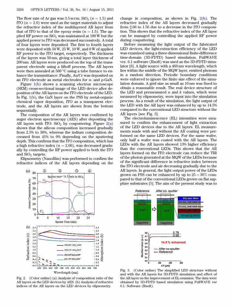
Before measuring the light output of the fabricatedLED devices, the light-extraction efficiency of the LEDwas examined using a three-dimensional finite-differencetime-domain (3D-FDTD) based simulation. FullWAVEver. 6.1 software (Rsoft) was used as the 3D-FDTD simu-lator [8]. A light source with a 460 nm wavelength, whichlies within the middle of the MQW layer, emitted photonsin a random direction. Periodic boundary conditionswere enforced to ignore the finite size effect of the simu-lation domain. A grid size as small as 10 nm was fixed toobtain a reasonable result. The real device structure ofthe LED and premeasured n and k values, which weremeasured by elipsometry, were input into the simulationprocess. As a result of the simulation, the light output ofthe LED with the AR layer was enhanced by up to 14.5%compared to the conventional LED structure without theAR layers [see Fig. 3].
The electroluminescence (EL) intensities were mea-sured to confirm the enhancement of light extractionof the LED devices due to the AR layers. EL measure-ments made with and without the AR coating were per-formed on the same LED devices. For the same wafer,only half a wafer was coated with the AR layers. TheLEDs with the AR layers showed 13% higher efficiencythan the conventional LEDs. This shows that the ARlayers formed on the ITO electrode can reduce the TIRof the photon generated at the MQW of the LEDs becauseof the significant difference in refractive index betweenthe ITO electrode and air decreasing gradually due to theAR layers. In general, the light output power of the LEDsgrown on PSS can be enhanced by up to 25 ∼ 30% com-pared to that of the conventional LEDs grown on flat sap-phire substrates [5]. The aim of the present study was to
Fig. 2. (Color online) (a) Analysis of composition ratio of theAR layers on the LED devices by AES. (b) Analysis of refractiveindices of the AR layers on the LED devices by elipsometry.
Fig. 3. (Color online) The simplified LED structure withoutand with the AR layers for 3D-FDTD simulation and effect ofthe AR layer on the improvement of EL emission. The data wereobtained by 3D-FDTD based simulation using FullWAVE ver6.1. Software (Rsoft).
3204 OPTICS LETTERS / Vol. 36, No. 16 / August 15, 2011

improve the light-extraction efficiency of LEDs grown onPSS, which is more meaningful than that of LEDs grownon flat sapphire substrates.I-V measurements were performed on the fabricated
LED devices to confirm the electrical properties. In allcases, identical I-V characteristics were observed, asshown in Fig. 4(b). The turns on voltage and leakage cur-rent levels of the LED devices were unchanged, whichsuggests that no electrical degeneration was induced dur-ing the fabrication of the AR layers on the LED device.
In summary, AR layers composed of ITO and SiO2 wereformed on the PSS LEDs by RF magnetron cosputtering.The EL intensities of the LEDs grown on PSS were en-hanced by up to 13% after forming the AR layers. Thisenhancement of the EL intensity is similar to that of theLED with the photonic crystal structure. On the otherhand, the LED with the AR layer is much easier andsimpler because it does not require a nanopatterningprocess. There was no degradation in the electrical prop-erties of the LED devices. Overall, GaN-based LEDs withhigh brightness can be fabricated without degrading theelectrical properties using a simple process.
This work is the outcome of a Manpower DevelopmentProgram for Energy & Resources supported by the Min-istry of Knowledge and Economy (MKE). It was partlysupported by the IT R&D program of MKE/IITA (2009F-025-01, Development of Core Technology for High Ef-ficiency Light-Emitting Diode based on New Concepts).
References
1. Y. Kawakami, Y. Narukawa, K. Omae, S. Fujita, andS. Nakamura, Phys. Status Solidi A 178, 331 (2000).
2. H. Benisty, H. De Neve, and C. Weisbuch, IEEE J. QuantumElectron. 34, 1632 (1998).
3. T. Fujii, Y. Gao, R. Sharma, E. L. Hu, S. P. DenBaars, andS. Nakamura, Appl. Phys. Lett. 84, 855 (2004).
4. M. Fujta, S. Takahashi, Y. Tanaka, T. Asano, and S. Noda,Science 308, 1296 (2005).
5. H. Gao, F. Yan, Y. Zhang, J. Li, Y. Zeng, and G. Wang, J. Appl.Phys. 103, 014314-1 (2008).
6. L. Rayleigh, Proc. London Math. Soc. s1-11, 51 (1879).7. K. J. Byeon, E. J. Hong, H. Park, J. Y. Cho, S. H. Lee, J. Jhin,
J. H. Baek, and H. Lee, Thin Solid Films 519, 2241 (2011).8. Fullwave 6.1 RSOFT design group (2008), http://www
.rsoftdesign.com.
Fig. 4. (Color online) (a) EL intensities of the LED deviceswith respect to wavelength with/without the AR layers, (b) I-Vcharacteristics of the LED devices with/without the AR layers.
August 15, 2011 / Vol. 36, No. 16 / OPTICS LETTERS 3205