for - atlas
TRANSCRIPT

Extended Abstracts of the 22nd (1990 International) Conference on Solid State Devices and Materials, Sendai, L9fr, pp. 39-42
Signal and Noise Modeling for Striped Channel Field-Effect Transistors
Yuji Ando, Masaaki Kuzuha.ra, Kazuhiko Onda,Norihiko Samoto, and Tomohiro Itoh
Microelectronics Research Laboratories,NEC Corporation, 4-1-1, Miyaaaki, Miyamae-ku,
Kawasaki 213, JAPAN
The cylindrical metal-semiconductor field-efect transistor (MESFET) has been studied for modeling thetwo-dimensional chargecontrol behaviors in striped channel field-eflect transistors (FETs). Modifying theclassical approach presented by van der Ziel and Pucei et al., the authors have developed the dc, small-signal, and noise model for cylindrical FETs. By using the present analysis, signal and noise properties forcylindrical FETs have been calculated and compa,red with the results for conventional FETs. Experimentallyobserved enhancement in charge- controllability is explained. Concerning noise properties, cylindrical FETsare shown to be equivalent to conventional FETs if transport properties are assumed to be identical. Thestriped channel FET is, however, considered to have a great potential as an ultra low-noise amplifier formicrowave and millimeter-wave frequencies due to the reduced short channel effects as well as superiortransport properties for quasi-one-dimension aJ ( Q tD ) electrons.
I. Introduction
With the resent progress in lithography and crystal growthtechniques, there have been considerable reports on examiningelectron transport properties in quasi-one-dimensionat (QlD)semiconductor wiresl)-s). One of interesting approachs is thestriped channel field-effect transistor (FET), which has parallelstripes of very narrow channels. Excellent dc and microwaveperformance for striped channel FETs has been demonstratedby Onda et al. 6) and Kawasaki et al.7) . The striped channelFET has some attractive {eatures:1) Superior electron transports due to QlD confinementl2) improved ch a^rge-controllability; and3) reduced short channel efects.Transport properties for QlD dlectrons have been studied byseveral authors 8)-10). There have been, however, no adequatemodel for explaining operation of striped channel FETs. Two-dimensional (2D) charge control behaviors make it difrcult tounderstand the operation of striped channel FETs. The aimof this paper is to propose a dc, small-signal, and noise modelfor striped channel FETs including the 2D cha;rge control char-acteristics. According to Rensch's approachl), the cylindricalmetal-semiconductor FET (MESFET) will be studied for mod-eling striped channel FETs.
II. DC Conditions for Cylindrical FETs
Figure 1 illustrates geometries for the striped channel FETand cylindrical MESFET. The cylindrical MESFET consists ofa cylindrical rod of conducting material with a radius o whichis surrounded by a circular gate with a length .Lo. FollowingPucel et aI. rL), the channel is divided into two regions. Ohm'slaw applies for region I, while in region II, electrons travelwith their saturation velocity or. According to the boundaryconditions for Poissonts equation, cylindrical coordinates (r, 6,r) are introduced. The applied gate voltage Vrr modulates thethickness of a depletion layer (a - D(r)) and hence the radiusof an active channel 6(r).
The gradual channel region (region I) for a cylindrical FETis analyzed based on the following assumptions:
B-1-7
1) The drift velocity u rises linea,rly with fields E" (< E');2) the longitudinal electric fields a^re negligible compared tothe transverse fields (Er), i."., En K E'; and
3) donors in the depletion layer are fully ionized.Poisson's equation for the potential t[r in region I is
FA-"1 u<*l
--lFo---l
Depletion layer
Fig. 1. Geometries for the striped channel FET.(o) A striped channel FET.(b) External appearance of a cylindrical MESFET.(c) Cross-sectional view of a cylindrical MESFET.
( LA,0---, gNd F ,
l;*Uilvr)=-: for D(o)Jr(a (to)
J !Ut(', a) = V(a) for 0 < r < b(o) (1b)
I itrr(o, a) = Vo, - Vt; (1.)
[*,r,c)=o (1d)
where Na is donor concentration, e permittivity, Vc, the gate-
source voltage, V6; the built-in voltage for the Schottky barrier,
l-Lg -l
and V(o) the channel potential at a point s. To simplify theanalysis, normaiized radii for the active channei are introduced.
,=9,*_ry,0=!+. (2)
From (1a)-(1d), V(o) is obtained in terms of tu.
v(r) -ye, + vt; = vr;+ + w2rnw) (s)
where Vpo = qNaaz f (2e). From (e), the threshold voltage is
Vn =uu, _?. (4)
Starting with the usual equations, one obtains drain current,length of region I, and the voltage drop for region I as
Ia = I.PZ, (5)
.2vLt = ffiI{(+; = Lo - Lr, (6)
and AVr = 2Ve"H(2) (7)respectively, where I, = qN4razu, and
( 1 1 1.-rrl_\- J i{r"(loo-il-s*(ln"-;)} for n=1,2,3,"'17 Inl = < 1"
.r2 ,r- ^tr', {^- - - n (8)\ ' [ ;ttt. P)'- (Ins)2] for n = o'
The potentia,i for the velocity saturation region (region II)is expressed by the sum o{ a pa,rticula^r solution for Poisson's
equation and a homogeneous solution Vz(t, c). The Lapiace's
equation for i[2 is
I t#.i*+ fttv,(r,r) = o (ea)
| ,y"r(r, nr)J 0 -- (eb)
1 U'r(o,r)=o (9")
I Pfo, L1) = -8,. (ed)( 0r'-The solution for above equations are apProximated by
, aEr,,,Pot(a-Lt)-rtrPolr\ //.llz(r, ,) = -Tsinhl-)Jo(?) (10)
PoL*4
where Jo is the Bessel function oI order 0 and Pot N 2.4048 is
a minimum .ralue for positive roots of Js(p) = 0. Therefore,
the channel voltage drop AVz through region II is
LV2 = "8" ,iot 1Po1'tr';. (11)Porta
From comparison between (11) a.nd the Grebene - Ghandhi
formulationlz), it is shown that the channel potential varies
more rapidly in cylindrical FETg than in conventional FETs.
Summing (7) and (1t), one obtains the drain voitage V4,'
III. Small-signal Parameters for Cylindrical FETs
From the analyses given in 13), we obtain the expressions
for transconductance:
gm = 4rearto, (12)
drain output resistance:
tJTrd=
-,+Teut
and gate'source capacitance:
Gg,=#rr.r*l"z),
where f, = ittl)2 cosh(@) - r), (rs).f"
t'p/ \ a ,
t, = Zlnp-{lop+i*t;l'ft'-}licosh(42;, (16)
a At
ta = *1rp'rnp - zH(a) cosh(
poIzl + parzj, (rla)Po' L ' a
^ ,' E.L. - . potLz\ . r r. -,and lcz = {{i(ffi - ln p) cosh( ff) - tl. OTb)
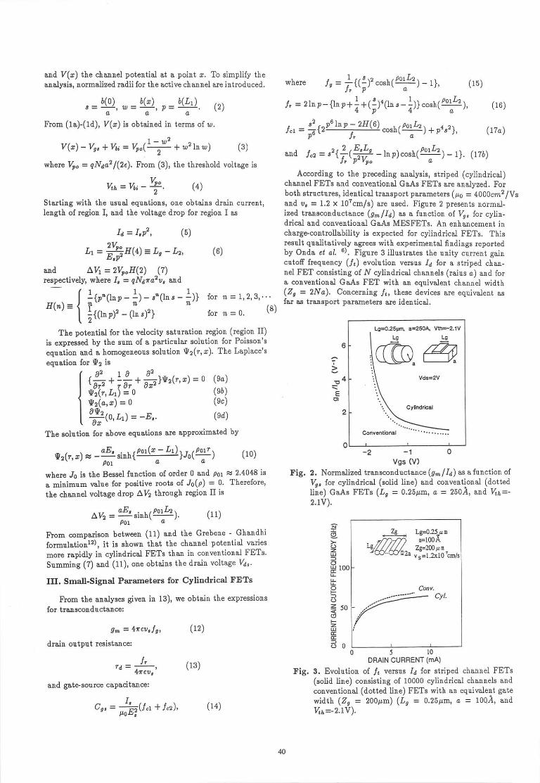
According to the preceding analysis, striped (cylindrical)channel FETs and conventiona,l. GaAs FETs are analyzed. Forboth structures, identical transport parameter. (po = 4000cm2 fYsand g, = L,2 x 107cm/s) are used. Figure 2 presents normal-ized transconductanc " (g* lIa) as a function of. Vs, for cylin-drical and conventional GaAs MESFETs. An enhancement incharge.controllability is expected for cylindrical FETs. Thisresult qualitatively agrees with experimental findings reportedby Onda et al. 6). Figure 3 illustrates the unity current gaincutof frequency (fi) evolution versus .Ia for a striped chan-nel FET consisting of N cylindrical channels (raius a) and fora conventiona,l GaAs FET with an equivalent channei width(Zc = 2No). Concerning fi, these devices are equivalent asfar as transport parameters are identical.
Lg=O.2SFm, a=250A, Vth=-2.1V
-2-1 0Vgs W)
Fig. 2. Norma,lized transconductance (g*lIa) as afunction ofVe, for cylindrical (solid }ine) and conventional (dottedIine) GaAs FETs (Lc = 0.25pm, a - 2504, and I{6--2.1v).
I
_4IT
=cq)
2
50
0
N!1-(5
oz,IJJ
r-rJ 1u-lJ-u.LLp()z,'
Fz.u.lctrE=O
,. ZE "
Lg=0.25#m
_ r/T)..//) a=100Atc/W//A^ Zs=2ffi pn -*'o vs=l'2x10'cm/s
Conv'cvl.
(13)
o o*o'*t u**=*r,tlo,
Fig. 3. Evolution of fi versus .Ia {or striped channel FETs(solid line) consisting of 10000 cylindrical channels and
conventional (dotted line) FETs with an equivalelt gate
width (Zc = 200pm) (Lc = 0.25p'm, a - L}QA, and
uh=_z.1v).(14)
40

IV. Noise Source Model for Cylindrical FETs
The noise model for cylindrical FETs was developed by
modifying the earlier work by van der 7i.11a)r1s), Statz-Haus-Pucelll) to a cylindrical FET version. The noise source isdivided in two pa,rts, i.e., Johnson noise from region I and
high-field difusion noise from region II. Only the final resultswill be written here. Details of an?Iyses are given in 13).
The drain voltage fluctuation v!1 caused by the Johnsonnoise is calculated based on the foltowing assumptionsll)'14)'1) Gradual channel approximation holds;2) the elementary noise voltage at a small segment (re ( r (os { doe) in region I is described by the Nyquist formula:
M,= 4kT"A,l Au'
D, N DnrTtwhere D6 is the high-field difusion coefrcientl8). Using (27),
we calculate the drain voltage fluctuation al" due to the difu-sion noise. The final results are
6=ffiP+blwith D - D{3*2ln)+}2 -4))
(30)
The gate and drain noise curents are correlated since they
originate both from the therma.l noise in channel. Fluctuatingfields and potentials modulate the carrier velocity as well as the
depletion layer thickness. Since the velocity change gives no
contribution to gate cutrents, the correlation coeff.cient (C11)
between ier and f41 becomes so much smaller than unity.
U = ry{,\()-r)-)1o 2)1=
-()r-lxt-arctan flXrrrl
where ) = exp(@) and b, = ap,
Modifying the Statz-Haus-Pucel model 11), the difusionnoise induced gate currents are calculated, as is seen by
Sqla\,laL?r'r'(t - 0)2J1(ppor)2 rr,, , nrlu r ul'
(27)
So*So
(28)
(2ea)
(18)Ia
where AJ is the frequency range' /c the Boltzmann constant,
and T* the efective noise temperaturel and
3) the intervalley scattering efects are included ba.sed on a
,imple expression for ?o presented by Baechtold 16):
ro x rs{L + o(#l\= ?o{1 + o(#)'}. ( 1e)
where ?e is the lattice temperature and 6 is an empirical pa-
rameter.The drain voltage fluctuation Atrl, due to an elementary noise
produced at o is obtained under ac open-circtit drain condi-
iioor. Summing M over region T,;'^ can be calculated as
E-rycosnzq@)[po+po]with ro = lalo; (zLa) P6 = 6p2a(o).
At high frequencies, there a.re induced noise currents on the
gate which is capacitively coupled to the channel. The induced
gate charge Ag1 due to an elementary noise prod.uc_ed at oe is
obtained with ac short-circuit drain conditionstt)'tt). Th" i*.duced gate currents can be derived by summin S Lih = ,2 Aq?
over region I. The fnal expression can be written as
6 = ry q#y coshz TPoLh ) lao + ncl (22)
with t = #tla(8)+r'r{(6)}
:2og2 -
r., iijalr-1I =:- -
i\f i?L'il.-(31)
(20)
( 21b)(32a)
and se = 6p2{f,H\) + r'}/(o)}. (320)
Since the noise in region II causes no velocity change, there isa full correlation between iaz and fez. Therefore their correla'tion coefficient is
1.^12with Ro = V{ft'2H(6) + r'7H1a) + 7A(to;1 (zsa)
and Rt = 6p2{n'2H(o) + n'1H(D +TH@)t, (23b)
Iarat:T'- ,rrr,cosrr(&rt2;
where
2DrnA(26)
L,o
where Ar and .A are thickness and cross-section for dipole lay-
ers, respectivelg D' is the difusion coefftcient, and ra is thecarrier density. In the Statz model, D, was assumed to be con-
stant. However, the Monte-Carlo calculations indicate that D'strongly depends on electric fieldsl?). Modi{ying the Einstein
relation, we approximate the D, variation versus Er(> E ) by
C22 = L. (33)
V. Noise Properties for Striped Channel FETs
The minimum noise f.gure F-io is given in terms of small-signal parameters, drain noise coefrcient P, gate noise coeffi-
cient R, and correlation coefficient C 11)'18), which are easilycalculated according to the preceding analysis. Noise prop-erties for striped channel FETs are studied and compared tothe conventional GaAs FETs with an equivalent channel width.Typical pa.rameters used for calculations are %i-0.8V, e f es=l).5,6=2, po=4000cm2/Vs t ue = 1.2 x 107cm/s, and D6=35cmz f s.
Identica,l para.meters are assumed for both FETs.
Noise coefrcients are calculated for striped channel andconventional FETs. Concerning P, R, and C at optimum .[a,
no important superiority is expected for striped channel FETs.Figure 4 illustrates Fnin dependence on .I4. The striped chan-nel FET shows a comparatively flat dependence of .F},;o onbias conditions. Rega,rding optimum flr;o values, these de-vices are equivalent. These results explain the experimenta.lfindings reported by KawasaLr et al. 7). The flor;o evolutionversus frequency is shown in Fig. 5.
So far, striped channel FETs have been compared to con-ventional FETs with identical pa.rameters. Figure 6 illustratesthe influence of saturation velocity on Fmin, It is shown thatsuperior transports of QlD channels dramatically improve noisecharacteristics for striped channel FETs.
(24)
*, - h{rr(6)- ry-r1,r,-}xo'-,')} *'ztff-i.es)The diffusion noise from region II.is interpreted as the shot
noise due to traveling dipole layersll) generated at the rate

I2GIlzLg=0.25Jun
a=100AZg=200 pn -vs=1.2x10'cm/sRg=Rs=0
Zs.i+--:+
n/7)-/7)re// / /// /!W-Waza
o o"o,*tu**=*r,tlo,
Fig. 4. Evolution oI F*;o (12GHz) vercus /a for cyiindrical(solid line) and conventional (dotted line) FETs withRc = R"=0. Other device parameters are the same as
those for Fig. 3.
VI. Conclusion
In summary, the cylindrical MESFET has been studied formodeling the 2D charge-control behaviors in striped channel
FETs. The authors have developed the dc, small-signal, and
noise modei for cylindrical FETs. By means of the present
theory, signal and noise properties for striped channel FETshave been analyzed. Features for noise properties o{ stripedchannel FETs are
1) Supposing transport properties are identical, striped a,nd
conventional FETs are equivalent concerning optimum ,F|;o;2) a high fi due to superior transport properties of Q1D elec-
trons improves the noise performance; and
3) suppressed short channel effects allow for reducing .L, with-out suffering from an increase in the drain noise.
Consequently, the striped channel FET is considered to have agreat potential to be a low-noise ampiifier for microwave and
millimet er- wa,ve frequencies.
Acknowledgment
The authors would like to thank K.Nakamura and F.Nihey formeaningful discussions and help. They would like to thank
H.Sakuma and T.Nozaki for their encouragement'
References
1) D.B.Rensch ef al. ; IEEE Trans.Electron Deaices ED-34(1e87) 2232.
2) K.IsmaiI et al. ; J.Vac.Sci.Technol.B 0 (1988) 1824.
3) M.Okada et al. ; Jpn.J.AppLPhys. 27 (1988) L2424.
a) K.Tsubaki ef al. ; Electron.Lett.24 (1988) 1267.
5) R.C.Clarkel Proc.IEEE/Cornell Cont. (New York 1983)
83.
6) K.Onda et al.i Proc.1989 IEDM (Washington,D.C. 1989)
L25.
7) H.Kawasaki ef aL ; presented at the 37th Spring Meetingof the Japan Society of Applied Physics and Related So-
cdetrec(Asaka 1990).
8) H.Sakal<t; Jpn.J.AppLPhys.tg (1980) L735.
9) J.P.Leburtonl J.AppI.Phss.56 (1984) 2850.
1O) T.Yamada and J.Sone; Proc.ICEM (Tokyo 1988) 96.
11) R.A.PuceI et aL ; Ailaanced Electron.Electron Phys. 38
(1e74) 1e5.
12) A.B.Grebene and S.K.Ghandhi; Solid-State Electron.\2(1e6e) E7s.
13) Y.Ando et al. ; submitted to IEEE Trans.Electron De-uices.
14) A.van der Ziel; Proc.IRE 50 (1962) 1808.
15) A.van der Ziel; Proc.IEEE 51 (1963) 461.
16) W.Baechtold; IEEE Trans.Electron Deuices ED-19 (1972)674.
17) Y.Ando and T.Itoh; IEEE Trans.ElectronDeuices 37 (1990)67.
1E) A.Cappy; IEEE Trans.Miulwaue Theory Tech. 36 (1988)1.
uJ
=(5rtr'ulooz3 0.5
=z=
oiltrfltrula
3o.tf
=z0
,,, zg " Le=o.l s m
,, f/fiffi ,JrooA1ffiazo Zg=200pn
t lff=ou3Rcv rJflz)tr
Fig. 5. .FL;, dependence on frequency for a striped channel
FET (solid lines) consisting o{ 10000 cylindrical channels
and for a conventional FET (dotted line) with an equiv-
alent gate width (Zo=2001'tm) (Ic = 0.1pm, a = 1004,
Vn=-2.1Y, and R, * Ro=O and aO). * and * denote
experimental data for striped and conventional HEMTs'resPectivelY ?).
l2GHzLg=o.Q pna=250AZy-200pnRg=Rs=0
vs (10 ?cm/s)
^nv J,,'Conv. I v
i t.t" ,z cyll
ZE,.#____--:+
"/&&,,
.i / ,.- cyl. t.5
Cyl. 1.8
510DRAIN CURRENT (mA)
6. Evolution o{ F*;" (12GHz) versus -Ia for a stripedchannel FET (solid lines) consisting of 4000 cylindricalchannels and for a conventional FET (dotted line) withan equivalent gate width (Zo=200p.m) (Lo = 0.25pm,a - 2504, andVlln=-2.1V). The tr, is ranged between 1.2
and 1.8 x107cm/s. For a conventiona^l FET, the resultis shown only for us = L.2 x 10?cm/s.
oIu.lE
9ttLlua6z3 o.t
===
0
Fis.