fiber-coupled nanophotonic devices for nonlinear optics and cavity qed
TRANSCRIPT

Fiber-coupled nanophotonic devices for nonlinear optics andcavity QED
Thesis by
Paul Edward Barclay
In Partial Fulfillment of the Requirements
for the Degree of
Doctor of Philosophy
California Institute of Technology
Pasadena, California
2007
(Defended May 23, 2007)

ii
c© 2007
Paul Edward Barclay
All Rights Reserved

iii
In memory of Larry Barclay

iv

v
Acknowledgments
Since my first visit to Caltech, Oskar Painter has been exceedingly generous with his time,
energy, and insight. Oskar’s enthusiasm for the work of his students, his curiosity, and his
desire to deeply understand whatever he is working on has never ceased to be inspiring, and
I feel fortunate to have learned so much about all aspects of research from him.
I have also been fortunate to interact with Hideo Mabuchi, with whom meetings always
ended with fresh ideas and optimism. Hideo’s combination of creativity and perspective is
something I hope to be able to replicate.
In my experience, the greatest strength of Caltech is its students. In Kartik Srinivasan,
with whom I have shared an office since arriving in Pasadena, one couldn’t ask for a better
colleague. Matthew Borselli never ceased being helpful. Thomas Johnson could always be
counted on to do things precisely. Building up the lab with this trio was a great experience,
and I’m sure that its future will be bright in the hands Raviv Perahia, Jessie Rosenberg,
Chris Michael, and Matt Eichenfeld. In the atomic physics lab, I was lucky to work closely
with Benjamin Lev. Ben always generously treated his hard work as if it were ours. With
help from Michael Armen, John Stockton, Andrew Berglund, Kevin McHale, and everyone
else in Mabuchi-lab, Joe Kerckhoff and I have had an exciting time catching up on Ben’s
considerable knowledge after he graduated, and I am grateful for Joe’s dedication.
Two people from my time at the University of British Columbia have had a lasting
influence. For two summers, Garry Clarke gave me the best job that I’m likely to ever have,
and in the process convinced me to go to graduate school. Jeff Young showed me how much
fun doing physics can be. I am ever thankful for their continued support and advice.
Away from school, Graeme Smith, the city of Los Angeles and its dedicated adventurers
on two wheels; Jesse Jackson and Nicholas Bradley and the geography of North America;
and other Canadian visitors have all kept me measurably distracted, which isn’t surprising
but is fortunate. Signe Bray could only have been a greater help to me if she had arrived

vi
in Pasadena earlier.
My brother David has always been a great friend and source of ideas, almost all of them
original. And of course my parents and grand parents have supported me tremendously.
My mother has never ceased giving encouragement, and my father was a tremendous source
of strength from whom I learned most of what I know.

vii
Abstract
The sub-wavelength optical confinement and low optical loss of nanophotonic devices dra-
matically enhances the interaction between light and matter within these structures. When
nanophotonic devices are combined with an efficient optical coupling channel, nonlinear
optical behavior can be observed at low power levels in weakly-nonlinear materials. In
a similar vein, when resonant atomic systems interact with nanophotonic devices, atom-
photon coupling effects can be observed at a single quanta level. Crucially, the chip based
nature of nanophotonics provides a scalable platform from which to study these effects.
This thesis addresses the use of nanophotonic devices in nonlinear and quantum optics,
including device design, optical coupling, fabrication and testing, modeling, and integration
with more complex systems. We present a fiber taper coupling technique that allows effi-
cient power transfer from an optical fiber into a photonic crystal waveguide. Greater than
97% power transfer into a silicon photonic crystal waveguide is demonstrated. This optical
channel is then connected to a high-Q (> 4 × 10⁴), ultra-small mode volume (V < (λ/n)3)
photonic crystal cavity, into which we couple > 44% of the photons input to a fiber. This
permits the observation of optical bistability in silicon for sub-mW input powers at telecom-
munication wavelengths.
To port this technology to cavity QED experiments at near-visible wavelengths, we also
study silicon nitride microdisk cavities at wavelengths near 852 nm, and observe resonances
with Q > 3×10⁶ and V < 15 (λ/n)3. This Q/V ratio is sufficiently high to reach the strong
coupling regime with cesium atoms. We then permanently align and mount a fiber taper
within the near-field an array of microdisks, and integrate this device with an atom chip,
creating an “atom-cavity chip” which can magnetically trap laser cooled atoms above the
microcavity. Calculations of the microcavity single atom sensitivity as a function of Q/V
are presented and compared with numerical simulations. Taking into account non-idealities,
these cavities should allow detection of single laser cooled cesium atoms.

viii
Contents
Acknowledgments v
Abstract vii
List of figures xxi
List of tables xxii
Glossary of Acronyms xxiii
Publications xxv
1 Introduction 1
1.1 Microcavities . . . . . . . . . . . . . . . . . . . . . . . . . . . . . . . . . . . 2
1.2 Fiber optic coupling at the nanoscale . . . . . . . . . . . . . . . . . . . . . . 3
1.3 Organization . . . . . . . . . . . . . . . . . . . . . . . . . . . . . . . . . . . 3
2 Interfacing photonic crystal waveguides with fiber tapers: design 5
2.1 Coupled-mode theory . . . . . . . . . . . . . . . . . . . . . . . . . . . . . . 7
2.2 k-space design . . . . . . . . . . . . . . . . . . . . . . . . . . . . . . . . . . 12
2.3 Contradirectional coupling in a square lattice PC . . . . . . . . . . . . . . . 16
2.4 Supermode calculations . . . . . . . . . . . . . . . . . . . . . . . . . . . . . 21
2.5 Conclusion . . . . . . . . . . . . . . . . . . . . . . . . . . . . . . . . . . . . 24
3 Efficient fiber to cavity coupling: theory and design 25
3.1 Efficient and ideal waveguide-cavity loading . . . . . . . . . . . . . . . . . . 26
3.2 Mode-matched cavity-waveguide design . . . . . . . . . . . . . . . . . . . . 28
3.3 Conclusion . . . . . . . . . . . . . . . . . . . . . . . . . . . . . . . . . . . . 32

ix
4 Probing photonic crystals with fiber tapers: experiment 34
4.1 Experimental details . . . . . . . . . . . . . . . . . . . . . . . . . . . . . . . 35
4.1.1 Fiber taper fabrication . . . . . . . . . . . . . . . . . . . . . . . . . . 36
4.1.2 Fiber probing measurement apparatus . . . . . . . . . . . . . . . . . 37
4.1.3 Photonic crystal fabrication . . . . . . . . . . . . . . . . . . . . . . . 38
4.2 Efficiently coupling into photonic crystal waveguides . . . . . . . . . . . . . 41
4.3 Real- and k-space waveguide probing . . . . . . . . . . . . . . . . . . . . . . 45
4.3.1 Bandstructure mapping . . . . . . . . . . . . . . . . . . . . . . . . . 46
4.3.2 Real-space mapping . . . . . . . . . . . . . . . . . . . . . . . . . . . 49
4.4 Efficient coupling into PC microcavities . . . . . . . . . . . . . . . . . . . . 50
4.5 Conclusion . . . . . . . . . . . . . . . . . . . . . . . . . . . . . . . . . . . . 56
5 Nonlinear optics in silicon photonic crystal cavities 57
5.1 Modeling nonlinear absorption and dispersion in a microcavity . . . . . . . 58
5.1.1 Nonlinear absorption . . . . . . . . . . . . . . . . . . . . . . . . . . . 58
5.1.2 Nonlinear and thermal dispersion . . . . . . . . . . . . . . . . . . . . 62
5.2 Nonlinear measurements . . . . . . . . . . . . . . . . . . . . . . . . . . . . . 66
5.3 Conclusion . . . . . . . . . . . . . . . . . . . . . . . . . . . . . . . . . . . . 72
6 Silicon nitride microdisk resonators 73
6.1 SiNx Microdisk fabrication . . . . . . . . . . . . . . . . . . . . . . . . . . . . 74
6.2 Microdisk mode simulations . . . . . . . . . . . . . . . . . . . . . . . . . . . 76
6.2.1 High Q modes of 9 μm diameter microdisks at 852 nm . . . . . . . . 78
6.2.2 Scaling of Qrad and V with microdisk diameter . . . . . . . . . . . . 80
6.3 Microdisk testing using a fiber taper . . . . . . . . . . . . . . . . . . . . . . 82
6.3.1 Waveguide microdisk coupling . . . . . . . . . . . . . . . . . . . . . 82
6.3.2 Microdisk testing at 852 nm . . . . . . . . . . . . . . . . . . . . . . . 84
6.3.3 Comparison with PECVD microdisks . . . . . . . . . . . . . . . . . 86
6.4 Resonance wavelength positioning . . . . . . . . . . . . . . . . . . . . . . . 87
6.5 Multidisk arrays . . . . . . . . . . . . . . . . . . . . . . . . . . . . . . . . . 88
6.6 Predicted microdisk cavity QED parameters . . . . . . . . . . . . . . . . . . 90
6.6.1 Cavity QED with Cs atoms . . . . . . . . . . . . . . . . . . . . . . . 92
6.6.2 Cavity QED with diamond NV centers . . . . . . . . . . . . . . . . . 93

x
6.6.3 Practical limitations . . . . . . . . . . . . . . . . . . . . . . . . . . . 94
6.7 Conclusion . . . . . . . . . . . . . . . . . . . . . . . . . . . . . . . . . . . . 96
7 An atom-cavity chip 97
7.1 Fiber coupled microcavities for atom chips . . . . . . . . . . . . . . . . . . . 98
7.1.1 Robust fiber mounting . . . . . . . . . . . . . . . . . . . . . . . . . . 98
7.1.2 Installation in a UHV chamber . . . . . . . . . . . . . . . . . . . . . 102
7.2 Microcavity surface sensitivity to Cs vapor . . . . . . . . . . . . . . . . . . . 103
7.3 Atom trapping on the atom-cavity chip . . . . . . . . . . . . . . . . . . . . 107
7.3.1 Atom chip basics . . . . . . . . . . . . . . . . . . . . . . . . . . . . . 107
7.3.2 Integrating cavities with atom chips . . . . . . . . . . . . . . . . . . 110
7.4 Conclusions and outlook . . . . . . . . . . . . . . . . . . . . . . . . . . . . . 114
8 Microcavity single atom detection 116
8.1 Atom induced modification of fiber coupled cavity response . . . . . . . . . 118
8.1.1 Single mode cavity . . . . . . . . . . . . . . . . . . . . . . . . . . . . 118
8.1.2 Whispering gallery mode cavity . . . . . . . . . . . . . . . . . . . . . 123
8.1.3 Simulations . . . . . . . . . . . . . . . . . . . . . . . . . . . . . . . . 128
8.2 Single atom detection: signal to noise . . . . . . . . . . . . . . . . . . . . . 132
8.2.1 Signal to noise ratio . . . . . . . . . . . . . . . . . . . . . . . . . . . 133
8.2.2 Photon detection schemes . . . . . . . . . . . . . . . . . . . . . . . . 135
8.2.3 Simulations . . . . . . . . . . . . . . . . . . . . . . . . . . . . . . . . 138
8.3 Summary . . . . . . . . . . . . . . . . . . . . . . . . . . . . . . . . . . . . . 142
A Bloch modes and coupled mode theory 144
A.1 Formulating Maxwell’s equations . . . . . . . . . . . . . . . . . . . . . . . . 144
A.1.1 Orthogonality of Bloch modes . . . . . . . . . . . . . . . . . . . . . . 146
A.1.2 Additional properties of Bloch modes . . . . . . . . . . . . . . . . . 148
A.2 Coupled mode equations: Lorentz reciprocity method . . . . . . . . . . . . 152
A.2.1 Coupling between two periodic waveguides . . . . . . . . . . . . . . 155
A.2.2 Power conservation . . . . . . . . . . . . . . . . . . . . . . . . . . . . 157
B Emitter-waveguide coupling 159
B.1 Coupled-mode analysis . . . . . . . . . . . . . . . . . . . . . . . . . . . . . . 159

xi
B.2 Field normalization . . . . . . . . . . . . . . . . . . . . . . . . . . . . . . . . 161
B.3 Coupling efficiency . . . . . . . . . . . . . . . . . . . . . . . . . . . . . . . . 162
Bibliography 164

xii
List of Figures
2.1 (a) Schematic of the coupling scheme, showing the four mode basis used in
the coupled mode theory. (b) Coupling geometry. In the case considered
here, the coupling is contra-directional. (c) Grading of the hole radius used
to form the waveguide, and a top view of the graded-defect compressed-lattice
(Λx/Λz = 0.8) waveguide unit cell. . . . . . . . . . . . . . . . . . . . . . . . . 6
2.2 Approximate bandstructure of fundamental even (TE-like) modes for a square
lattice PC of air holes with radius r/Λ = 0.35 in a slab of thickness d = 0.75Λ
and dielectric constant ε = 11.56. Calculated using an effective index of neffTE =
2.64, which corresponds to the propagation constant of the fundamental TE
mode of the untextured slab. The inset shows the first Brillouin-zone of a
rectangular lattice. . . . . . . . . . . . . . . . . . . . . . . . . . . . . . . . . . 13
2.3 Projection of the square lattice bandstructure onto the first Brillouin-zone
of a line defect with the same periodicity of the lattice and oriented in the
X1 → Γ direction. Bandedges whose modes have dominant wavenumbers in
theX1 → Γ direction (i.e. k = kz) are drawn with solid black lines. Bandedges
whose modes have dominant wavenumbers in the X2 → M direction (i.e.
k = kz z + π/Λxx) are drawn with dashed black lines. . . . . . . . . . . . . . 14
2.4 Approximate projected bandstructure for (a) donor type and (b) acceptor
type, compressed square lattice waveguides. Possible defect modes and the
fundamental fiber taper mode are indicated by the dashed lines. . . . . . . . 15

xiii
2.5 3D FDTD calculated bandstructure for the waveguide shown in Fig. 2.1(c).
The dark shaded regions indicate continuums of unbound modes. The dashed
lines are the dispersion of fiber tapers with radius r = 0.8Λz = 1Λx (upper
line) and r = 1.5Λz = 1.875Λx (lower line). The solid black lines are the air
(upper line) and fiber (lower line) light lines. The energies and wavenumbers
of modes TE1 and B are ωΛz/2π = 0.304 and 0.373 at βΛz/2π = 0.350 and
0.438 respectively. . . . . . . . . . . . . . . . . . . . . . . . . . . . . . . . . . 17
2.6 Mode TE1 field profiles calculated using FDTD. Dominant magnetic field com-
ponent (a) |By(x, y = 0, z)|; and (b) |By(x, y, z = 0)|; (c) Dominant electric
field component transverse Fourier transform |Ex(kx, y = 0, z)|. Note that the
dominant transverse Fourier components are near kx = 0. . . . . . . . . . . 18
2.7 (a) Power coupled to PC mode TE1 from a tapered fiber with radius r = 1.15Λx
placed with a d = Λx gap above the PC as a function of detuning from phase
matching and coupler length. (b) Power coupled at ω = ω0 to the forward and
backward propagating PC and fiber modes as a function of coupler length. . 19
2.8 Mode B field profiles calculated using FDTD. Dominant magnetic field com-
ponent (a) |By(x, y = 0, z)|, (b) |By(x, y, z = 0)|. (c) Dominant electric field
component transverse Fourier transform |Ex(kx, y = 0, z)|. Note that the
dominant transverse Fourier components are near kx = ±π/Λx. . . . . . . . 20
2.9 Power coupled to PC mode B from a tapered fiber with radius r = 1.55Λx
placed with a d = Λx gap above the PC as a function of detuning from phase
matching and coupler length. . . . . . . . . . . . . . . . . . . . . . . . . . . . 22
2.10 (a) FDTD calculated bandstructure of the full fiber taper photonic crystal
system. The fiber taper has a radius r = 1.17Λz = 1.46Λx, and is d =
Λz = 1.25Λx above the PC waveguide. The TE1-like and fiber-like dispersion
is identified, and the symmetric and antisymmetric superpositions of these
modes at the anti-crossing are labeled by the ± signs. (b) The By(x, y, 0)
component of the symmetric supermode. (c) The By(x, y, 0) component of the
antisymmetric supermode. . . . . . . . . . . . . . . . . . . . . . . . . . . . . 23

xiv
3.1 (a) Schematic of the fiber taper to PC cavity coupling scheme. The blue arrow
represents the input light, some of which is coupled contradirectionally into the
PC waveguide. The green arrow represents the light reflected by the PC cavity
and recollected in the backwards propagating fiber mode. The red colored
region represents the cavity mode and its radiation pattern. (b) Illustration of
the fiber-PC cavity coupling process. The dashed line represents the “local”
band-edge frequency of the photonic crystal along the waveguide axis. The step
discontinuity in the bandedge at the PC waveguide - PC cavity interface is due
to a jump in the longitudinal (z) lattice constant. The parabolic “potential”
is a result of the longitudinal grade in hole radius of the PC cavity. The
bandwidth of the waveguide is represented by the gray shaded area. Coupling
between the cavity mode of interest (frequency ω0) and the mode matched PC
waveguide mode (ωWG = ω0) is represented by γe0, coupling to radiating PC
waveguide modes is represented by γej>0, and intrinsic cavity loss is represented
by γi. . . . . . . . . . . . . . . . . . . . . . . . . . . . . . . . . . . . . . . . . 26
3.2 (a,b) High-Q defect cavity mode profiles. Plots of the magnetic field pattern
are shown in (a) the x − z plane (|By(x, y = 0, z)|), and (b) the x − y plane
(|By(x, y, z = 0)|). (c,d) PC waveguide TE1 mode field profiles, taken in the
(a) the x− z plane and (b) the x− y plane. . . . . . . . . . . . . . . . . . . 30
3.3 Coupling from the defect cavity to the PC waveguide for varying waveguide
lattice compression at instances in time when the cavity magnetic field is a
minimum (left) and a maximum (right). The envelope modulating the waveg-
uide field is a standing wave caused by interference with reflections from the
boundary of the computational domain. The diagonal radiation pattern of the
cavity is due to coupling to the square lattice M points, and is sufficiently
small to ensure a cavity Q of ≈ 105. |B| for (a) ΛWGx /ΛWG
z = 20/20 (b)
ΛWGx /ΛWG
z = 20/25 (ratio used in the previous section) (c) ΛWGx /ΛWG
z = 20/29. 32
xv
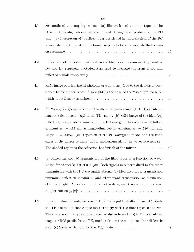
4.1 Schematic of the coupling scheme. (a) Illustration of the fiber taper in the
“U-mount” configuration that is employed during taper probing of the PC
chip. (b) Illustration of the fiber taper positioned in the near field of the PC
waveguide, and the contra-directional coupling between waveguide that occurs
on-resonance. . . . . . . . . . . . . . . . . . . . . . . . . . . . . . . . . . . . . 35
4.2 Illustration of the optical path within the fiber optic measurement apparatus.
DT and DR represent photodetectors used to measure the transmitted and
reflected signals respectively. . . . . . . . . . . . . . . . . . . . . . . . . . . . 38
4.3 SEM image of a fabricated photonic crystal array. One of the devices is posi-
tioned below a fiber taper. Also visible is the edge of the “isolation” mesa on
which the PC array is defined. . . . . . . . . . . . . . . . . . . . . . . . . . . 40
4.4 (a) Waveguide geometry and finite-difference time-domain (FDTD) calculated
magnetic field profile (By) of the TE1 mode. (b) SEM image of the high (r1)
reflectivity waveguide termination. The PC waveguide has a transverse lattice
constant Λx = 415 nm, a longitudinal lattice constant Λz = 536 nm, and
length L = 200Λz . (c) Dispersion of the PC waveguide mode, and the band
edges of the mirror termination for momentum along the waveguide axis (z).
The shaded region is the reflection bandwidth of the mirror. . . . . . . . . . 42
4.5 (a) Reflection and (b) transmission of the fiber taper as a function of wave-
length for a taper height of 0.20 μm. Both signals were normalized to the taper
transmission with the PC waveguide absent. (c) Measured taper transmission
minimum, reflection maximum, and off-resonant transmission as a function
of taper height. Also shown are fits to the data, and the resulting predicted
coupler efficiency, |κ|2. . . . . . . . . . . . . . . . . . . . . . . . . . . . . . . . 45
4.6 (a) Approximate bandstructure of the PC waveguide studied in Sec. 4.3. Only
the TE-like modes that couple most strongly with the fiber taper are shown.
The dispersion of a typical fiber taper is also indicated. (b) FDTD calculated
magnetic field profile for the TE1 mode, taken in the mid-plane of the dielectric
slab. (c) Same as (b), but for the TE2 mode. . . . . . . . . . . . . . . . . . . 47

xvi
4.7 3D FDTD calculated dispersion of the TE1 (dotted line), TE2 (dashed line),
and TM1 (dot-dashed line) modes for the (a) un-thinned (tg = 340 nm), and
(b) thinned (tg = 300 nm) graded lattice PC waveguide membrane structure
(nSi = 3.4). Measured transmission through the fiber taper as a function of
wavelength and position along the tapered fiber for (c) un-thinned sample and
(d) thinned sample (different tapers were used for the thinned and un-thinned
samples, so the transmission versus lc data cannot be compared directly).
Transmission minimum (phase-matched point) for each mode in the (e) un-
thinned and (f) thinned sample as a function of propagation constant. In
(a-b), the lightly shaded regions correspond to the tuning range of the laser
source used. . . . . . . . . . . . . . . . . . . . . . . . . . . . . . . . . . . . . . 48
4.8 Coupling characteristics from the fundamental fiber taper mode to the TE1
PC waveguide mode of the thinned sample (tg = 300 nm). Transmission versus
wavelength for (a) 1.9μm and (b) 1.0 μm diameter taper coupling regions for
varying taper-PC waveguide gap, g. Transmission in (a,b) has been normalized
to the transmission through the fiber-taper in absence of the PC waveguide. . 49
4.9 Coupling characteristics from the fundamental fiber taper mode to the TE1
PC waveguide mode of the thinned sample (tg = 300 nm). (a) 1−Tmin versus
lateral position (Δx) of the 1.0 μm diameter fiber taper relative to the center
of the PC waveguide (g = 400 nm). (b) Transmission versus wavelength for
Δx ∼ 1 μm. Transmission in (a-b) has been normalized to the transmission
through the fiber-taper in absence of the PC waveguide. . . . . . . . . . . . . 50
4.10 SEM image of an integrated PC waveguide-PC cavity sample. The PC cavity
and PC waveguide have lattice constants Λ ∼ 430 nm, Λx ∼ 430 nm, and
Λz ∼ 550 nm. The surrounding silicon material has been removed to form a
diagonal trench and an isolated mesa structure to enable fiber taper probing. 51
4.11 (a) Illustration of the device and fiber taper orientation for (i) efficient PC
waveguide mediated taper probing of the cavity, and (ii) direct taper probing
of the cavity. (b) Normalized depth of the transmission resonance (ΔT ) at
λo ∼ 1589.7, as a function of lateral taper displacement relative to the center
of the PC cavity, during direct taper probing (taper in orientation (ii)). . . . 52

xvii
4.12 (a) Measured reflected taper signal as a function of input wavelength (taper
diameter d ∼ 1 μm, taper height g = 0.80 μm). The sharp dip at λ ∼ 1589.7
nm, highlighted in panel (b), corresponds to coupling to the A02 cavity mode.
(c) Maximum reflected signal (slightly detuned from the A02 resonance line),
and resonance reflection contrast as a function of taper height. The dashed
line at ΔR = 0.6 shows the PC waveguide-cavity drop efficiency, which is
independent of the fiber taper position for g ≥ 0.8 μm. . . . . . . . . . . . . . 54
5.1 (a) Measured cavity response as a function of input wavelength, for varying
PC waveguide power (taper diameter d ∼ 1 μm, taper height g = 0.80 μm). . 67
5.2 (a) Power dropped (Pd) into the cavity as a function of power in the PC
waveguide (Pi). The dashed line shows the expected result in absence of
nonlinear cavity loss. (b) Resonance wavelength shift as a function of internal
cavity energy. Solid blue lines in both Figs. show simulated results. . . . . . 68
5.3 (a) Simulated effective quality factors for the different PC cavity loss channels
as a function of power dropped into the cavity. (b) Contributions from the
modeled dispersive processes to the PC cavity resonance wavelength shift as a
function of power dropped into the cavity. (Simulation parameters: ηlin ∼ 0.40,
ΓthdT/dPabs = 27 K/mW, τ−1 ∼ 0.0067+(1.4×10⁻⁷)N0.94 where N has units
of cm−3 and τ has units of ns.) . . . . . . . . . . . . . . . . . . . . . . . . . 70
5.4 Dependence of free-carrier lifetime on free-carrier density (red dots) as found
by fitting Δλo(Pi) and Pd(Pi) with the constant material and modal param-
eter values of Table 5.1, and for effective PC cavity thermal resistance of
ΓthdT/dPabs = 27 K/mW and linear absorption fraction ηlin = 0.40. The
solid blue line corresponds to a smooth curve fit to the point-by-point least-
squared fit data given by τ−1 ∼ 0.0067+(1.4×10⁻⁷)N0.94, where N is in units
of cm−3 and τ is in ns. . . . . . . . . . . . . . . . . . . . . . . . . . . . . . . . 71
6.1 (a) SEM image of a SiNx microdisk after the ICP-RIE dry etching, but be-
fore the resist removal and undercutting of the underlying Si layer. Note the
smoothness of the sidewalls. (b) SEM image of a fully processed SiNx microdisk. 75

xviii
6.2 Electric field magnitude distribution of the four highest Qrad modes with res-
onance wavelengths near 852 nm for a 9 μm diameter, 250 nm thick SiNx
microdisk with a 45 degree sidewall profile. The calculated radiation quality
factor Qrad, optical mode volume Vo (assuming a standing wave mode), and
normalized peak exterior energy density η are also indicated for each mode. . 77
6.3 Resonance wavelength and Qrad of the lowest radial order (highest m andQrad)
modes with resonance wavelengths near 852 nm for a 9 μm diameter, 250 nm
thick SiNx microdisk with a 45 degree sidewall profile. . . . . . . . . . . . . . 79
6.4 FEM calculated Vo and Qrad of the p = 1 TE and TM modes as a function
of microdisk diameter, for h = 250 nm. (a) Qrad at λ = 852 nm. (b) Vo
at λ = 852 nm. (c) Qrad at λ = 637 nm. (d) Vo at λ = 637 nm. In all of
the mode volume calculations, it was assumed that the microdisk supports
standing wave modes. . . . . . . . . . . . . . . . . . . . . . . . . . . . . . . . 81
6.5 (a) Schematic of fiber taper coupling to a microdisk traveling wave mode. (b)
Generalization of the coupling process depicted in (a) to represent a microdisk
that supports standing wave modes. s and t are the input and output field
amplitudes of the fiber taper field, respectively (see Ch. 8). . . . . . . . . . . 82
6.6 Taper transmission when the taper is aligned close the perimeter of a 9 μm
diameter microdisk. This wide wavelength scan was obtained by performing a
DC motor sweep of the laser diode grating position. This data shows a typical
“family” of microdisk modes. The high frequency noise on the off-resonance
background is due to etalon effects in the laser. . . . . . . . . . . . . . . . . . 84
6.7 Fiber taper transmission when the taper is positioned in the near field of a 9 μm
diameter microdisk, for two fiber taper positions. The data in (a), (b), and
(c) are for different nominally identical microdisks fabricated simultaneously
on the same chip. The red lines are fits using a model that includes coupling
between the microdisk and the tapers, as well as between traveling wave modes
of the microdisk. . . . . . . . . . . . . . . . . . . . . . . . . . . . . . . . . . 85
6.8 (a) Shift in resonance wavelength as a function of HF dip time. Resonance
lineshape (b) before, and (c) after a 60 s HF dip. Note that the Q of the
resonance has not degraded. . . . . . . . . . . . . . . . . . . . . . . . . . . . . 87

xix
6.9 (a) Optical microscope image of part of an array of 10 microdisks, aligned with
a fiber taper. (b) Transmission spectra of the fiber taper when it is aligned
with an array of 10 microdisks. . . . . . . . . . . . . . . . . . . . . . . . . . . 89
6.10 Cavity QED parameters for a Cs atom in the microdisk near field, as a function
of microdisk diameter. The Cs atom is taken to be at the field maximum
outside of the microdisk. The microdisk thickness is h = 250 nm, and λ ∼852 nm. In calculating κ, Q = min
[4 × 10⁶, Qrad
]. (a,b) Interaction and
decoherence rates for the fundamental (a) TE mode, (b) TM mode. (c) Strong-
coupling parameter. (d) Bad cavity parameter. . . . . . . . . . . . . . . . . 93
6.11 Cavity QED parameters for an diamond NV center interacting with the mi-
crodisk near field, as a function of microdisk diameter. The NV center is taken
to be at the field maximum outside of the microdisk. The microdisk thickness
is h = 250 nm, and λ ∼ 637 nm. In calculating κ, Q = min[4 × 10⁶, Qrad
].
(a,b) Interaction and decoherence rates for the fundamental (a) TE mode, (b)
TM mode. (c) Strong coupling parameter. (d) Bad cavity parameter. . . . . 95
7.1 Illustration of a fiber taper mounted in a “U” configuration to a glass slide.
The fiber taper is bonded to the glass slide using UV curable epoxy. . . . . . 99
7.2 (a) Illustration of a fiber coupled photonic chip integrated with an atom chip.
(b) SEM image of a fiber taper permanently mounted to a microdisk using
epoxy microjoints. . . . . . . . . . . . . . . . . . . . . . . . . . . . . . . . . . 100
7.3 Resonance wavelength shift of the 9 μm diameter SiNx microdisk studied in Ch.
6 as a function of time exposed to Cs. The Cs partial pressure was 10−9−10−8
Torr. . . . . . . . . . . . . . . . . . . . . . . . . . . . . . . . . . . . . . . . . . 104
7.4 Simulated accumulated Cs film thickness as a function of time for varying
background pressure. For the upper curve, at the time indicated by the dashed
vertical line the Cs partial pressure is reduced by an order of magnitude. . . 106
7.5 (a) Illustration of a magnetic trap formed by superimposing a homogeneous
magnetic bias field with the magnetic field generated from current in a wire
directed out of the page. This trap offers confinement in the 2D plane of
the page. (b) Top view of two wire configurations that provide 3D magnetic
trapping when combined with a homogeneous bias field. . . . . . . . . . . . . 108

xx
7.6 Illustration of the laser beam and microwire geometry used to form the atom
chip mirror-MOT. During the MOT formation, current flows through the “u”
section of the “h” microwire circuit. . . . . . . . . . . . . . . . . . . . . . . . 109
7.7 Illustration of the laser beam and microwire geometry used to form a mirror-
MOT when the cavity-mirror is integrated with the atom chip. (a) Top view,
(b) end view, (c) side view. The zoomed-in detail (d) shows how a MOT can
be formed above an array of cavities on an otherwise uniform mirror. The
shadow from the cavities only extends above the surface as high as the cavity
footprint. . . . . . . . . . . . . . . . . . . . . . . . . . . . . . . . . . . . . . 111
7.8 SEM images of a cavity-mirror chip. The mesa contains a 3 × 10 array of 9
μm diameter microdisks, and is isolated by ∼ 20 μm above the surrounding
gold coated Si substrate. . . . . . . . . . . . . . . . . . . . . . . . . . . . . . . 112
7.9 Photoluminescence images of laser cooled atoms being delivered to the micro-
cavity array on the atom chip. The red-colored area highlights the position of
the cavity array. The atom-cavity chip is oriented as in Fig. 7.7(b). Each im-
age is taken by halting the experiment at the specified time after the transfer
from the the macro mirror-MOT to the cavity has begun, zeroing the magnetic
fields, and exciting the atoms using the MOT beams. The resulting photo-
luminescence, as well as light scattered by the atom chip surface, is imaged
using a zoom lens, and is collected by a CCD camera. . . . . . . . . . . . . . 113
8.1 Depiction of microdisk atom detection experiment. . . . . . . . . . . . . . . . 117
8.2 Effect of an atom on the response of a fiber coupled single-mode cavity as a
function of (left) on-resonance waveguide input power (Δωc = Δωa = 0), and
(right) drive field detuning Δωc with Pi � Ps and Δωa = Δωc, for varying
cavity quality factor: (a) Q = 106, (b) Q = 105, (c) Q = 104. In all of the
simulations, λo = 852 nm, g/2π = 1 GHz, γa/2π = 0.005 GHz, K = 0.52
(Te,o = 0.1), and both fully-quantum and semiclassical solutions were used, as
indicated. For the spectra on the right, the semiclassical and fully-quantum
results cannot be differentiated by eye. . . . . . . . . . . . . . . . . . . . . . 129

xxi
8.3 Same simulations as in Fig. 8.3, but including a degenerate whispering gallery
mode (|β| = 0). Also shown is the reflected waveguide signal. Both fully-
quantum and semiclassical solutions were used, as indicated. For the spectra
on the right, the semiclassical and fully-quantum results can not be differenti-
ated by eye. The power dependent calculations in (a) were limited to Pi < Ps
for computational reasons. . . . . . . . . . . . . . . . . . . . . . . . . . . . . 131
8.4 Same simulations as in Fig. 8.3, but with microcavity induced coupling be-
tween the degenerate whispering gallery modes (|β|/2π = 9 [GHz], β real).
The atomic dipole is detuned by −|β| from the uncoupled cavity resonance
frequency, so that is spectrally aligned with the lower frequency standing wave
mode. Although γe is unchanged from the simulation results in Figs. 8.3 and
8.2, in the standing wave basis K → K ′ = K/(K + 1) = 0.34. Also shown
is the reflected waveguide signal. The semiclassical and fully-quantum results
cannot be differentiated by eye. . . . . . . . . . . . . . . . . . . . . . . . . . 132
8.5 Calculated SNR for a fiber coupled single mode (left) and degenerate whis-
pering gallery mode (right) microcavity with g/2π = 1 GHz and (a) Q = 106,
(b) Q = 105, (c) Q = 104. In all of the calculations, λo = 852 nm, γa/2π =
0.005 GHz, Δωa = Δωc = 0, K = 0.52 (Te,o = 0.1). The various detector
parameters are given in Table 8.1. The power dependent calculation in (a)
was limited to Pi < Ps for computational reasons. . . . . . . . . . . . . . . . 141
8.6 Calculated SNR for fiber coupled single mode microcavities with g/2π =
10 GHz and (a) Q = 105, (b) Q = 104. In all of the calculations, λo = 852 nm,
γa/2π = 0.005 GHz, Δωa = Δωc = 0, K = 0.52 (Te,o = 0.1). The various
detector parameters are given in Table 8.1. . . . . . . . . . . . . . . . . . . . 142

xxii
List of Tables
5.1 Nonlinear optical coefficients for the Si photonic crystal microcavity. . . . . . 69
8.1 Photodetector parameters . . . . . . . . . . . . . . . . . . . . . . . . . . . . . 140

xxiii
Glossary of acronyms
APD Avalanche photodiode.
cQED Cavity quantum electrodynamics.
CCD Charge coupled detector.
CW Continuous wave.
e-beam Electron beam.
FCA Free carrier absorption.
FCD Free carrier dispersion.
FDTD Finite difference time domain.
FEM Finite element method.
FEMLAB Finite element method software package distributed by Comsol.
FSR Free spectral range.
HD Heterodyne.
ICP-RIE Inductively coupled reactive ion etch.
MOT Magneto-optical trap.
LIAD Light induced atom desorption.
LPCVD Low pressure chemical vapor deposition.
SEM Scanning electron microscope.
SNR Signal to noise ratio.

xxiv
SOI Silicon on insulator.
SPCM Single photon counting module.
TE Transverse electric.
TM Transverse magnetic.
TPA Two photon absorption.
NV Nitrogen vacancy.
PC Photonic crystal.
PCWG Photonic crystal waveguide.
PECVD Plasma enhanced chemical vapor deposition.
PMMA Polymethyl methacrylate.
RPM Revolutions per minute.
Q Quality factor.
QED Quantum electrodynamics.
UV Ultra-violet.
UHV Ultra high vacuum.
V Mode volume.

xxv
Publications
• P. E. Barclay, K. Srinivasan, M. Borselli, and O. Painter. Experimental demonstration
of evanescent coupling from optical fibre tapers to photonic crystal waveguides. IEE
Elec. Lett., 39(11) 842–844, 2003.
• K. Srinivasan, P. E. Barclay, O. Painter, J. Chen, A. X. Cho, and C. Gmachl. Exper-
imental demonstration of a high quality factor photonic crystal microcavity. Appl.
Phys. Lett., 83(10) 1915–1917, 2003.
• O. Painter, K. Srinivasan, and P. E. Barclay. Wannier-like equation for the resonant
cavity modes of locally perturbed photonic crystals. Phys. Rev. B, 68(3) 035214,
2003.
• P. E. Barclay, K. Srinivasan, and O. Painter. Design of photonic crystal waveguides
for evanescent coupling to optical fiber tapers and integration with high-Q cavities.
J. Opt. Soc. Am. B, 20(11) 2274–2284, 2003.
• P. E. Barclay, K. Srinivasan, M. Borselli, and O. Painter. Efficient input and output
optical fiber coupling to a photonic crystal waveguide. Opt. Lett., 29(7) 697–699,
2004.
• B. Lev, K. Srinivasan, P. E. Barclay, O. Painter, and H. Mabuchi. Feasibility of
detecting single atoms using photonic bandgap cavities. Nanotechnology, 15 S556–
S561, 2004.
• S. A. Maier, P. E. Barclay, T. J. Johnson, M. D. Friedman, and O. Painter. Low-
loss fiber accessible plasmon waveguide for planar energy guiding and sensing. Appl.
Phys. Lett., 84(20) 3990–3992, 2004.
• P. E. Barclay, K. Srinivasan, M. Borselli, and O. Painter. Probing the dispersive

xxvi
and spatial properties of planar photonic crystal waveguide modes via highly efficient
coupling from optical fiber tapers. Appl. Phys. Lett., 85(1) 4–6, 2004.
• K. Srinivasan, P. E Barclay, and O. Painter. Fabrication-tolerant high quality factor
photonic crystal microcavities. Opt. Expr., 12(7) 1458–1463, 2004.
• K. Srinivasan, P. E. Barclay, M. Borselli, and O. Painter. Optical-fiber based mea-
surement of an ultra-small volume high-Q photonic crystal microcavity. Phys. Rev.
B, 70 081306(R), 2004.
• M. Borselli, K. Srinivasan, P. E. Barclay, and O. Painter. Rayleigh scattering, mode
coupling, and optical loss in silicon microdisks. Appl. Phys. Lett., 85(17) 3693–3695,
2004.
• P. E. Barclay, K. Srinivasan, and O. Painter. Nonlinear response of silicon photonic
crystal microresonators excited via an integrated waveguide and a fiber taper. Opt.
Expr., 13 801–820, 2005.
• K. Srinivasan, P. E. Barclay, M. Borselli, and O. Painter. An Optical-Fiber-Based
Probe for Photonic Crystal Microcavities. IEEE JSAC, 23 1321–1329, 2005.
• S. A. Maier, M. D. Friedman, P. E. Barclay, and O. Painter. Experimental demon-
stration of fiber-accessible metal nanoparticle plasmon waveguides for planar energy
guiding and sensing. Appl. Phys. Lett., 86(7) 071103, 2005.
• K. Srinivasan, M. Borselli, T. J. Johnson, P. E. Barclay, O. Painter, A. Stintz, and
S. Krishna. Optical loss and lasing characteristics of high-quality-factor AlGaAs
microdisk resonators with embedded quantum dots. Appl. Phys. Lett., 86 151106,
2005.
• P. E. Barclay, B. Lev, K. Srinivasan, H. Mabuchi, and O. Painter. Integration of
fiber coupled high-Q SiNx microdisks with atom chips. Appl. Phys. Lett., 89 131108,
2006.

1
Chapter 1
Introduction
From afar, fabrication of nanoscale optical components can appear to be predominantly mo-
tivated by the same forces that have driven developments in the microelectronics industry,
where we have become accustomed to equating smaller with more powerful. Unsurpris-
ingly, to a large degree this intuition is correct. Optical chips containing dense arrays of
devices have the potential for high bandwidth data processing, and already play a role in the
telecommunications industry [1, 2, 3]. However, as a scientist, the motivation for minitur-
ization can come from elsewhere: the desire to study optical effects that cannot be observed
easily, if at all, without the help of wavelength scale confinement of light. Reassuringly,
these two views of optical miniturization are not in conflict. Instead, these interests drive
each other: Novel chip-scale optical phenomena often find applications in practical devices,
and the usefulness of a scalable, integrated optical platform is not lost on physicists wanting
to study increasingly complex systems.
The work in this thesis is focused on optical nanostructures, with both of these perspec-
tives in mind. We study chip-based optical waveguides and microcavities, first developing
tools for optically accessing and characterizing them, and then using them in experiments
in nonlinear optics and cavity QED [4, 5, 6]. Each of these experiments is immediately
relevant to applications that leverage the chip-scale nature of the structures. Nonlinear
optical effects in silicon (Si) nanostructures can be used for low power on-chip all-optical
switching, while integrated nanophotonic circuits promise to improve the robustness and
scalability of cavity QED based quantum information processing resources.

2
1.1 Microcavities
Optical microcavities [7] confine light to wavelength scale volumes for relatively long times,
and are the cornerstone of nanophotonics. At resonant frequencies, they enhance the local
electromagnetic energy density, and support extremely large field strengths for low input
powers. Generally speaking, the high quality factor (Q) and small mode volume (V ) of
microcavities make them sensitive to intensive and extensive properties, respectively, of
their host environment. For example, a high-Q cavity can be extremely sensitive to small
changes in the bulk susceptibility of its environment, while a small V cavity can be sensitive
to local changes.
While microcavities can be fabricated from a wide range of geometries, including pho-
tonic crystal [8, 9, 10, 11, 12] and whispering gallery mode [13, 14, 15, 16, 17] resonators,
any given microcavity can be characterized by Q and V . These quantities are defined in
terms of the local field supported by the microcavity. For a microcavity resonance excited
by a single photon, the field maxima Emax inside the cavity is simply written as
Emax =
√�ω
2εV, (1.1)
where ω is the optical frequency of the resonance, and ε is the dielectric constant of the
microcavity at the field maximum. To maintain this field strength in steady state, it is
necessary to replenish the microcavity with new photons at the same rate at which they
leak out due to imperfections or limitations in the microcavity design. This decay rate is
related to Q:dN
dt= −ω
QN, (1.2)
where N is the number of photons stored in the cavity at a given time t. From energy
conservation, this indicates that the power required to store N photons in the cavity scales
as 1/Q. Using the above two equations, for a given power dropped into a cavity, the peak
intracavity energy density can be shown to scale with Q/V .
This enhancement is the basis for a large number of recent experiments in microcavity
nonlinear optics, whose power thresholds scale in a nonlinear fashion with V/Q. Examples
includes low threshold Raman lasers [18, 19, 20], parametric down conversion [21], and
radiation pressure induced mechanical oscilation [22, 23]. Recently, low power nonlinear all-

3
optical switching [24, 25, 26] has been observed. Large Q/V is also essential for experiments
in cavity QED [4, 5, 6], which study the coherent energy exchange between single photons
and single atoms [27, 28, 29] or quantum dots [30, 31, 32, 33]. Within the cavity, the atom-
photon interaction rate and photon dissipation rate scale with 1/V 1/2 and 1/Q, respectively,
and when the atom-photon interaction rate is sufficiently strong compared to the photon
and atomic decoherence rates, the coupled atom-cavity system can be used in applications
such as single photon generation [34, 35, 36, 37] and quantum state transfer [38, 39] for
quantum information processing.
1.2 Fiber optic coupling at the nanoscale
In addition to requiring large field enhancements and photon lifetimes, any useful application
of microcavities in nonlinear and quantum optics demands an efficient optical interface
between the microcavity and external optics. The mismatch in both spatial dimensions and
refractive index between wavelength-scale photonics and conventional fiber optics is severe,
and without engineering a transition between the macro- and the nano-scale, the loss of
optical fidelity is extremely high.
Fiber tapers [40, 41] are versatile tools that make this transition adiabatically. They
have been used to efficiently excite resonances in whispering gallery mode cavities [42, 43,
15, 44, 45], and as discussed in this thesis, photonic crystal waveguides [46, 47, 48] and
microcavities [11]. The highly integrated nature of chip based photonics also comes to our
aid, as microcavities can be efficiently sourced from on-chip waveguides [25, 49] that are in
turn coupled to the outside world. Using these tools to establish efficient optical channels
between the laboratory and nanophotonic devices, the next challenge is to integrate fiber
coupled devices with more complex experimental systems, such as those used in neutral
atom based cavity QED experiments.
1.3 Organization
Many of the topics discussed above are studied in detail in this thesis. In Ch. 2 and
Ch. 3, we theoretically examine the problem of coupling light into and out of photonic
crystal waveguides, and propose a new technique using fiber tapers. This technique is put

4
into practice in Ch. 4, where we demonstrate nearly perfect coupling at telecommunication
wavelengths between a fiber taper and a Si photonic crystal waveguide, and use the taper to
probe the dispersive and spatial properties of the bound photonic crystal waveguide modes.
Efficient coupling between the photonic crystal waveguide and a high-Q, ultra-small V
photonic crystal microcavity is also demonstrated. The nonlinear optical properties of this
Si microcavity are studied in Ch. 5, where optical bistability is observed at sub-mW input
powers.
In Ch. 6, our focus shifts to studying microcavities suitable for cavity QED experiments
with neutral alkali atoms at near visible wavelengths. We show that SiNx is an excellent
material for microcavities operating in this wavelength range, and demonstrate extremely
high Q/V microdisk cavities. These microdisks are integrated with atom chips in Ch.
7, where a method for robust fiber coupling is demonstrated, and the resulting atom-
cavity chip is installed in an atomic physics apparatus used for neutral atom trapping and
manipulation, with the aim of perfoming cavity QED experiments fully “on-chip.” Finally,
the possibility of detecting single atoms delivered to the microcavity using the atom chip
is studied theoretically in Ch. 8, where general scaling laws for single atom sensitivity are
derived and verified numerically.

5
Chapter 2
Interfacing photonic crystal waveguideswith fiber tapers: design
The utility of photonic crystal (PC) devices relies heavily upon one’s ability to efficiently
couple light into and out of them. At the outset of the work contained in this thesis, no
efficient technique had been demonstrated for efficiently exciting guided modes of planar
photonic crystal waveguide structures. Initial photonic crystal waveguide experiments [52,
53] relied upon end-fire coupling between single mode fibers and the cleaved facet of a PC
waveguide, and exbited extremely small coupling efficiency (< 20 dB) because of the extreme
spatial and refractive index mismatch between subwavelength high-index PC structures and
optical fibers.
A number of methods for overcoming this problem have been studied. Perhaps the
most obvious approach is to use adiabatic transitions [54, 55, 56] from “standard” ridge
waveguides to source PC waveguides. However, coupling from fibers into high refractive
index ridge waveguides poses similar problems, and requires the use of on-chip spot-size
converters [57, 49, 58, 53] for high efficiency. Other groups have developed free-space grating
assisted coupling techniques [59, 60] that utilize the periodicity of the photonic crystal
waveguide to scatter light at near-normal incidence into bound photonic crystal waveguide
modes, with modest efficiency.
Our approach differs fundamentally from those described above. Rather than design
on-chip coupling interfaces, we decided to bury the transition between fiber optics and
nanophotonics within fiber. Evanescent coupling between a fiber taper [40] and a PC
waveguide, as detailed schematically in Fig. 2.1, makes use of the inherent dispersive prop-
erties of PCs to enable guided-wave coupling between waveguides with nearly ideal coupling
efficiency. A single fiber taper used in this manner can function as an adjustable “wafer

6
Undercut Region (n = 1)
λ / 2 Slab (n = 3.4)
Substrate
Extended Defect WGEtched Holes (n = 1)
(c)
(b)
zx
y
Λx
Λz
0.35
0.28r / Λz
F
PC
PC
F+
+-
-
(a)
Figure 2.1: (a) Schematic of the coupling scheme, showing the four mode basis used in thecoupled mode theory. (b) Coupling geometry. In the case considered here, the coupling iscontra-directional. (c) Grading of the hole radius used to form the waveguide, and a topview of the graded-defect compressed-lattice (Λx/Λz = 0.8) waveguide unit cell.
scale probe” for testing of multiple devices on a planar chip.
Evanescent coupling
In the simplest picture, evanescent coupling between two parallel waveguides requires that
there exist (in the frequency range of interest) a pair of modes, one from each waveguide,
that share a common momentum component down the waveguide (phase-matching), and
for which their transverse profiles and electric field polarizations are similar. A weak spatial
overlap of the evanescent tails of each mode can then result in significant power transfer

7
between waveguides. Full power transfer requires that, in addition, no other radiation or
guided modes of either waveguide participate in the coupling, either due to a large phase
mismatch and/or weak transverse overlap. Fiber taper coupling has been shown to be
extremely valuable in this regard (in comparison to simple prism coupling, which involves
a continuum of modes), and was first used to provide near perfect single mode coupling to
dielectric microsphere [61, 42, 62] and toroid [14] resonators for ultra sensitive measurement
of high-Q whispering gallery modes. In a similar manner, fiber taper probes can be used to
couple to two dimensional PC membrane waveguides, thanks to their undercut air-bridge
structure that suppresses radiation from the fiber into the substrate, and their zone-folded
dispersion that enables phase matching between the dissimilar fiber and PC modes. Thus,
by designing a PC waveguide whose defect mode has a transverse field profile that sufficiently
overlaps the fiber taper’s, efficient power transfer between the waveguides can be achieved.
Furthermore, the flexibility in lattice engineering afforded by PCs allows this waveguide to
be designed to couple efficiently to PC defect cavities, providing a fiber-PC waveguide-PC
cavity optical probe.
In the remainder of this chapter, closely following Ref. [63], we discuss the design of a
PC waveguide that satisfies the requirements outlined above. In Sec. 2.1, a simple coupled
mode theory that models coupling between a fiber taper and a PC is presented, and the
desired waveguide properties are illuminated mathematically and discussed in more detail.
In Sec. 2.2, a general k-space analysis of bulk PC bandstructures is used to determine which
types of defect modes have the desired properties. The results from these sections are then
applied to the design and analysis of a PC waveguide in a square lattice in Sec. 2.3, and are
further illustrated with FDTD supermode calculations in Sec. 2.4.
2.1 Coupled-mode theory
It has long been realized that modes in translationally invariant waveguides with differing
dielectric constants can be phase-matched with the aid of a grating, so it is not surpris-
ing that the intrinsic discrete translational symmetry of PC waveguides and the resulting
zone-folded dispersion of their modes allows PCs to be phase-matched with a large class of
dissimilar waveguides, including tapered fibers. Grating mediated phase-matching schemes
have been studied extensively, beginning with the research of microwave traveling wave

8
tubes [64], and, more recently, of optical devices such as filters, directional couplers, and
distributed feedback lasers (Ref. [65] and references therein). However, because the dielec-
tric contrast of a PC grating is large, the fiber-PC coupling picture differs from that of
a traditional (weak) grating assisted coupler, and rather than analyze coupling between
plane-waves of the untextured waveguides, we must consider the Bloch eigenmodes of the
PC waveguide. Although rigorous coupled mode theories for Bloch modes have been devel-
oped in the context of non-linear perturbations to Bragg fibers [66], photonic crystals [67],
and coupled-resonator optical waveguides [68], none of these formalisms consider coupling
between parallel waveguides. In order to evaluate the properties of evanescent coupling be-
tween a fiber and a PC defect waveguide, a coupled mode theory is presented in this section
that can approximately predict the power transfer between the PC Bloch modes and the
fiber planewave modes as a function of propagation distance, transverse coupling strength,
and phase-mismatch. More detailed derivations of the following equations, as well as some
useful properties of Bloch modes, are given in Appendix A.
The physical system being modeled is specified by the dielectric constants of the inter-
acting waveguides εμ(r), each of which individually supports a set of modes Eμν (r), where
μ labels the waveguides and ν labels the eigenmodes of each waveguide. For e−iωt time
dependence, Maxwell’s equations require that each of these modes satisfies the eigenvalue
equation
∇ × ∇ × Eμν (r) = ω2εμ(r)Eμ
ν (r) (2.1)
where ω = ω/c is the free space wavenumber.
The fundamental approximation of waveguide coupled mode theories is that after some
propagation distance the field of the composite system represented by ε(r) = ε1 ∩ ε2...∩ εn
can be approximated by some linear combination of the modes of the constituent systems
represented by εμ(r):
E(r) =∑μν
Cμν (z)Eμ
ν (r) (2.2)
where it has been assumed that the modes are propagating in the ±z direction, or more
precisely that the power flux of the individual modes in the z direction is constant. When
considering continuums of delocalized modes, an integral replaces the discrete sum. If εμ(r)
is periodic in z so that εμ(x, y, z+Λz) = εμ(x, y, z), by Bloch’s theorem [69] the eigenmodes

9
have z dependence of the form Eμν (x, y, z + Λz) = eiβνΛzEμ
ν (x, y, z), and Eq. (2.1) becomes
Hβνeμβν
(r) = ω2εμ(r)eμβν
(r) (2.3)
where
Hβν = (−β2ν z × z + iβν(z × ∇ + ∇ × z) + ∇ × ∇)×, (2.4)
eμβν
(x, y, z + Λz) = eμβν
(x, y, z), and −π/Λz < βν ≤ π/Λz (i.e., βν is restricted to the first
Brillouin zone) so that the eigenmodes are not over-counted. Equation (2.3) is often solved
as an eigenvalue problem for ων parameterized by the wavenumber β, giving a dispersion
relation ων = ων(β). In linear media, only modes degenerate in ω have non-zero time
averaged coupling over typical laboratory time-scales, and it is convenient to label the modes
at fixed ω by their wavenumber βν(ω). Both conventions are equivalent and interchangeable.
Typically (as discussed below), for weak coupling only modes nearly resonant in β (modulo
a reciprocal lattice vector 2π/Λz) to the exciting field need to be included in expansion
(2.2); this is the basic assumption of the coupled mode theory. For weak coupling, this
assumption that only nearly resonant modes interact is reasonable; however, the question
of completeness is less clear. In general, Eq. (2.2) cannot satisfy Maxwell’s equations since
the eigenmodes of waveguide μ1 do not satisfy the boundary conditions of waveguide μ2,
and vice versa. This issue was debated vigorously in the late 80s, but was not resolved,
and is well summarized in Ref. [70]. In Ref. [71], Haus and Snyder showed that in some
cases the ansatz Eq. (2.2) can be improved by modifying the modes used in the expansion
so that they satisfy the boundary conditions of the composite system. This improvement
is non-trivial in the case of a photonic crystal slab, however, and will not be used here.
This deficiency is minimized for TE-like modes but exists nonetheless if the waveguides lack
translational invariance or planar geometry, as is the case in photonic crystal waveguides
and fiber tapers, respectively. Despite this limitation, we proceed under the assumption
that in the limit of weak coupling the resulting model is a useful design tool that correctly
describes the dependence of the coupling on the physical parameters but whose absolute
results may deviate from the exact values.
In order to formulate coupled-mode equations, we assume that ansatz Eq. (2.2) is a
solution to Maxwell’s equations for the hybrid system and employ the Lorentz reciprocity
relationship [72] which must hold for any two solutions to Maxwell’s equations in non-

10
magnetic materials:
∂
∂z
∫z(E1 × H∗
2 + E∗2 × H1) · z dx dy = i ω
∫zE1 ·E∗
2(ε1 − ε∗2)dx dy (2.5)
where (E,H)1,2 satisfy Maxwell’s equations for ε1,2. Setting
E1 =∑
j
Cj(z)Ej(r)
E2 = Ei (2.6)
and correspondingly
ε1 = ε
ε2 = εi (2.7)
where the single index, i = (μi, νi), labeling both the waveguide and the mode is adopted
for clarity, and substituting Eqs. (2.6-2.7) into Eq. (2.5), the following power-conserving
coupled mode equations are obtained:
PijdCj
dz= i ωKijCj (2.8)
where
Pij(z) =∫
z(E∗
i × Hj + Ej × H∗i ) · z dx dy (2.9)
Kij(z) =∫
zE∗
i ·Ej(ε− εj)dx dy (2.10)
and it has been assumed that all dielectric constants are real. Equation (2.8) is similar to
the coupled mode equations given in Ref. [73], with the only differences arising from the
fact that no specific form of z dependence of the eigenmodes has been assumed. When
the mode amplitudes are fixed at some z = z0, Eq. (2.8) can easily be solved numerically,
giving a transfer matrix that maps the amplitudes at z0 to z0 + L. In order to correctly
model an experimental setup, the amplitude of the modes propagating in the +z direction
should be fixed at z0, and the amplitude of the modes propagating in the −z direction

11
should be fixed at z0 + L. Since Eq. (2.8) is linear and origin independent, Eq. (2.8) can
be solved with these mixed boundary conditions by first calculating the transfer matrix
(which maps C±i (z0) → C±
i (z0 + L) where the sign superscript represents the propagating
direction of mode j ) and then transforming it to the appropriate scattering matrix (which
maps C+i (z0) → C+
i (z0 + L) and C−i (z0 + L) → C−
i (z0)).
From Eq. (2.5), the diagonal terms, Pii, of the power matrix are constant, and are typ-
ically normalized to plus or minus unity depending on the sign of the group velocity of
mode i. Additionally it can be shown that Bloch modes of the same waveguide are power
orthogonal so that Pij = 0 if εi = εj and Ei = Ej . However, modes from neighboring waveg-
uides are not power orthogonal, resulting in non-zero off-diagonal z-dependent components
in Pij which must be retained for Eq. (2.8) to be power conserving. In the fiber taper-PC
system, the PC fields’ z-dependence is the product of a planewave part and a periodic part,
whereas fiber fields have planewave-like z-dependence. Expanding the periodic part of the
PC field as well the PC dielectric constant in a Fourier series, the z-dependence of Pij and
Kij can be written in terms of superpositions of exp [i (βi − βj − 2πm/Λz) z] terms, where
m is an integer. For weak coupling (dCj/dz � 1/λ), only the slowly varying component
(compared to λ) of Kij significantly couples the amplitude coefficients Ci and Cj over lab-
oratory length scales of interest. This reasoning is analogous to (for example) that used in
the time-domain rotating-wave approximation in quantum mechanics, and is often used to
derive approximate analytic solutions to coupled mode equations describing two mode elec-
tromagnetic systems in the presence of weak gratings [3]. Because of the strong dielectric
contrast of the PC, the problem here is more complex; however, the fundamental results
from the simple cases hold: In order to observe significant power exchange between modes,
their wavenumbers’ β must differ by approximately a reciprocal lattice vector 2πm/Λz , and
the larger the phase matched driving terms, the stronger the coupling. The mixing of the
Fourier components of the PC Bloch mode and dielectric constant is the most significant
effect captured by this coupled mode theory compared to standard weak grating theories.
Physically, this allows coupling between PC and fiber modes that is mediated either directly
by a Fourier coefficient of the PC Bloch mode (the dominant effect here) or indirectly by
the PC dielectric acting like a grating (a higher order effect). Optimizing the magnitude of
these coefficients, and as a result, the coupling from the fiber mode to the desired photonic
crystal waveguide mode is discussed in the next section.

12
2.2 k-space design
Photonic crystal defect waveguides are formed by introducing a line of defects into an
otherwise two or three dimensionally periodic PC. Here we consider pseudo-2D membrane
structures whose typical geometry is shown in Fig. 2.1. In absence of the defects, the
eigenmodes of the bulk 2D slab are Bloch modes whose in-plane wavenumber, k, is a good
mode label and who are bound to the slab if ω(k) is below the cladding and substrate light-
lines; i.e., ω(k) < ck/nc, s, where ns and nc are the indices of refraction of the substrate
and cladding respectively. (We will not consider bound modes that exist at special points
in ω − k space above the light-line, as shown in [74].) The air-bridge membrane structures
considered here have nc = ns = 1, maximizing the area in ω − k space where bound modes
exist, and also ensuring that the bound modes of a fiber taper (nf ≈ 1.45) do not leak into
the PC substrate.
The PC modes can be classified as either even or odd, depending on their parity under
inversion about the x− z mirror plane of the slab (see Fig. 2.1 for the coordinate system),
and it can be shown that the lowest order even modes (i.e., modes with no zeros in the y
direction) are TE-like, while the lowest order odd modes (i.e., modes with one zero in the y
direction) are TM-like. We only consider coupling to TE-like modes (the fiber can couple to
either). Furthermore, we assume that the slab is thin enough to ensure that the frequencies
of the second order odd modes (which are also TE-like) are above the frequency range
of interest, so that only the fundamental TE-like mode needs to be considered. Figure
2.2 shows the approximate bandstructure of the fundamental TE-like modes of the bulk
square-lattice PC slab considered in this paper. This bandstructure is calculated using an
effective index 2D planewave expansion model that takes into account the finite thickness
of the slab but neglects the vector nature of the field, providing a useful guide for analyzing
the ω − k space properties of potential PC waveguide modes.
When a line defect is introduced, the discrete translational symmetry of the PC is
reduced from two to one dimension, and consequently only the component β of k paral-
lel to the line defect remains a good mode-label. The corresponding Bloch eigenmodes
must satisfy Eq. (2.3) and the resulting band structure is approximately obtained by
projecting the bulk PC bandstructure onto the first Brillouin zone of the defect unit cell
(ω1D(β) = ω2D(k |k · u = β) where unit vector u is parallel to the line defect) as shown

13
Γ X M X Γ
0
0.5
Λ /
λ
1 2
X
X M
Γ
1
2
k
Λπ
x
Λπ
y
Figure 2.2: Approximate bandstructure of fundamental even (TE-like) modes for a squarelattice PC of air holes with radius r/Λ = 0.35 in a slab of thickness d = 0.75Λ and dielectricconstant ε = 11.56. Calculated using an effective index of neff
TE = 2.64, which correspondsto the propagation constant of the fundamental TE mode of the untextured slab. The insetshows the first Brillouin-zone of a rectangular lattice.
in Fig. 2.3, and by a discrete set of modes whose field is localized to the defect region.
In k-space the localized and delocalized modes are characterized by β and a transverse
wavenumber distribution. The projection creates continuums of delocalized modes in ω− β
space over which the dominant transverse wavenumber varies smoothly and approximates
that of the bulk mode from which it is projected. For small defects, the localized modes
are superpositions of the delocalized modes at the top or bottom of the continuum re-
gions, depending on whether the defect is an acceptor or donor type. By identifying from
which bulk modes these continuum “band-edges” are projected, we can thus approximately
determine the dominant transverse wavenumber of the defect modes. Given a bulk 2D
bandstructure, the k-space properties of the defect modes associated with any defect ge-
ometry can therefore be approximately determined without resorting to computationally
expensive waveguide simulations.

14
ΓΓ Χ ΧΜ
Λ /
λ
0.5
X - Γ bandedge
Continuum modes0
1 2
X - M projected bandedge2
1
Figure 2.3: Projection of the square lattice bandstructure onto the first Brillouin-zone of aline defect with the same periodicity of the lattice and oriented in the X1 → Γ direction.Bandedges whose modes have dominant wavenumbers in the X1 → Γ direction (i.e. k = kz)are drawn with solid black lines. Bandedges whose modes have dominant wavenumbers inthe X2 →M direction (i.e. k = kz z + π/Λxx) are drawn with dashed black lines.
To determine what PC waveguide k-space properties are desirable for efficient coupling,
it is necessary to consider the fiber taper mode properties. Guided fiber taper modes are
confined to the region in ω−β space bounded by the air and fiber (usually silica, nf ≈ 1.45)
light lines, as shown in Fig. 2.4, which immediately limits the PC modes with which the
fiber can phase match. A suitable fiber typically has a radius on the order of a PC lattice
constant, and the corresponding linearly polarized fundamental fiber mode (HE11±HE1−1)
is broad compared to the PC feature size. As a result, PC modes that are highly oscillatory
in the transverse direction will not couple well to the fiber, since their transverse coupling
coefficients derived in the previous section will be small. PC modes that maximize the
coupling coefficient must thus have a transverse wavenumber distribution that is peaked at
zero (i.e., has a large transverse DC component). This corresponds to defect modes that
are dominantly formed from bulk PC modes whose k is parallel to the defect (the X1 → Γ

15
Γ Χ
Λ /
λ
0
0.5
Γ ΧDonor defect Acceptor defect
Γ - X defect mode
1 1
X - M defect mode
Fiber mode
1
2
Slab continuum modes
Radiation modes
TE-1
B
(a) (b)
n
1
f n
1
f
Figure 2.4: Approximate projected bandstructure for (a) donor type and (b) acceptor type,compressed square lattice waveguides. Possible defect modes and the fundamental fibertaper mode are indicated by the dashed lines.
direction here).
These ideas are illustrated in Fig. 2.4, which shows a bulk compressed square lattice
band structure projected onto the first Brillouin zone of a line defect in the X1 → Γ
direction. The compressed lattice is used for reasons discussed below and is not essential
for the analysis. The approximate dispersion of localized modes formed by both donor
and acceptor type defects are shown, and modes whose transverse wavenumber distribution
satisfy the requirements discussed above are indicated. It is not required that the defect
modes be in a full photonic bandgap for the coupling scheme considered here. As in the
case of other novel PC devices such as lasers [75] and high-Q cavities [76] that have been
realized in small bandgap square lattice PCs, localized waveguide modes can exist without
a full in-plane bandgap [77]. That being said, for mode selective coupling to be possible it
is necessary that the defect mode exists in a “window” in ω − β space, where the nearest

16
mode degenerate in ω is detuned sufficiently in β to suppress coupling, due to its large phase
mismatch. Although lattice compression is not required to achieve this, it is sometimes
advantageous to distort the lattice in order to optimize the window in ω − β space, as was
done here. Compressing the lattice in the transverse direction effectively raises the energy
of the bands at the X2 point and M point in Fig. 2.3, modifying the projection of the full
bandstructure onto the first Brillouin zone of the defect waveguide, as reflected in Fig. 2.4.
Once an appropriate lattice and defect waveguide type have been selected, and the ap-
proximate location of the desired mode in ω−β space determined using these approximate
2D techniques, 3D finite-difference time-domain (FDTD) can be used to numerically cal-
culate the field profiles and exact dispersion of the 3D PC waveguide eigenmodes. The
numerical results are used in turn in the coupled mode theory to model the coupling to the
tapered fiber modes. These design principles are applied in the next section to design a
compressed square lattice PC defect waveguide that can couple efficiently to fiber tapers.
2.3 Contradirectional coupling in a square lattice PC
The PC waveguide modes considered in this paper are formed within an optically thin
(thickness tg = 3/4Λx) semiconductor (n = 3.4) membrane perforated with a square array
of air holes. From the approximate band structure for the bulk compressed square lattice
waveguide shown in Fig. 2.4, there are several potential defect waveguide modes that are
not in a continuum and that can phase match with a fiber taper (whose typical disper-
sion is also shown). Of these modes, only waveguide mode A has the desired transverse
wavenumber components: It comes off a bandedge projected from the X1 → Γ band of the
bulk bandstructure, while the other modes come from M → X2 bandedges. Because mode
TE1 is not in a full frequency bandgap, it is not an obvious candidate in the context of the
existing literature, which focuses on waveguide modes within a full bandgap. However, as
we will show, this mode is confined to the defect region, can be coupled selectively with a
fiber taper, and can be used to probe high-Q cavity modes (Ch. 3).
A 3D FDTD calculation of the even bandstructure for the graded waveguide of Fig.
2.1(c) in a compressed (Λx/Λz = 0.8) square lattice is shown in Fig. 2.5. Modes that are
odd about the x− z mirror plane are not shown in this plot; however, it was verified that
the frequencies of the TE-like odd modes were higher than that of mode TE1 in the region

17
Λ /
λz
β Λ / 2πz
B0.4
0.150.32 0.5
TE-1TE-1
Figure 2.5: 3D FDTD calculated bandstructure for the waveguide shown in Fig. 2.1(c).The dark shaded regions indicate continuums of unbound modes. The dashed lines are thedispersion of fiber tapers with radius r = 0.8Λz = 1Λx (upper line) and r = 1.5Λz = 1.875Λx
(lower line). The solid black lines are the air (upper line) and fiber (lower line) light lines.The energies and wavenumbers of modes TE1 and B are ωΛz/2π = 0.304 and 0.373 atβΛz/2π = 0.350 and 0.438 respectively.
of interest (circle “TE1” in Figs. 2.4 - 2.5). Although other donor defect geometries could
have been used, the hole radius grading and the lattice compression used here are important
design features of the waveguide for a number of reasons. As discussed in Ch. 3, the field
profile of Ref. [76]’s graded cavity mode is very similar to that of waveguide mode TE1
suggesting that this waveguide mode is ideal for tunneling light into and out of these cavities.
In addition, the compressed lattice provides for: (i) expansion of the window in ω−β space
supporting defect donor type modes that can phase match with the taper; (ii) an increase
in the slope of the defect mode dispersion, resulting in increased coupler bandwidth; and
(iii) matching of the frequencies of the waveguide mode and the uncompressed defect cavity

18
(a)
(b)
(c)
x / Λx5-5
z /
Λz
0
2
x / Λx5-5
y /
Λz
-2
2
Λ k / πx x-3 3
z /
Λz
0
1
-1 1
Figure 2.6: Mode TE1 field profiles calculated using FDTD. Dominant magnetic field com-ponent (a) |By(x, y = 0, z)|; and (b) |By(x, y, z = 0)|; (c) Dominant electric field componenttransverse Fourier transform |Ex(kx, y = 0, z)|. Note that the dominant transverse Fouriercomponents are near kx = 0.
donor mode without any stitching of the lattice required. (Choosing ΛPCx = ΛCav
x requires
that ΛPCz /ΛCav
z = ωCav/ωPC.) The two sets of localized states expected from Fig. 2.4 are
seen to form, one originating from the X1-point in the 2D reciprocal lattice, and the other
from the M -point. The most localized of each set are the fundamental (transverse) modes,
which we label as mode TE1 and mode B in Figs. 2.4 - 2.5. The magnetic field profiles and
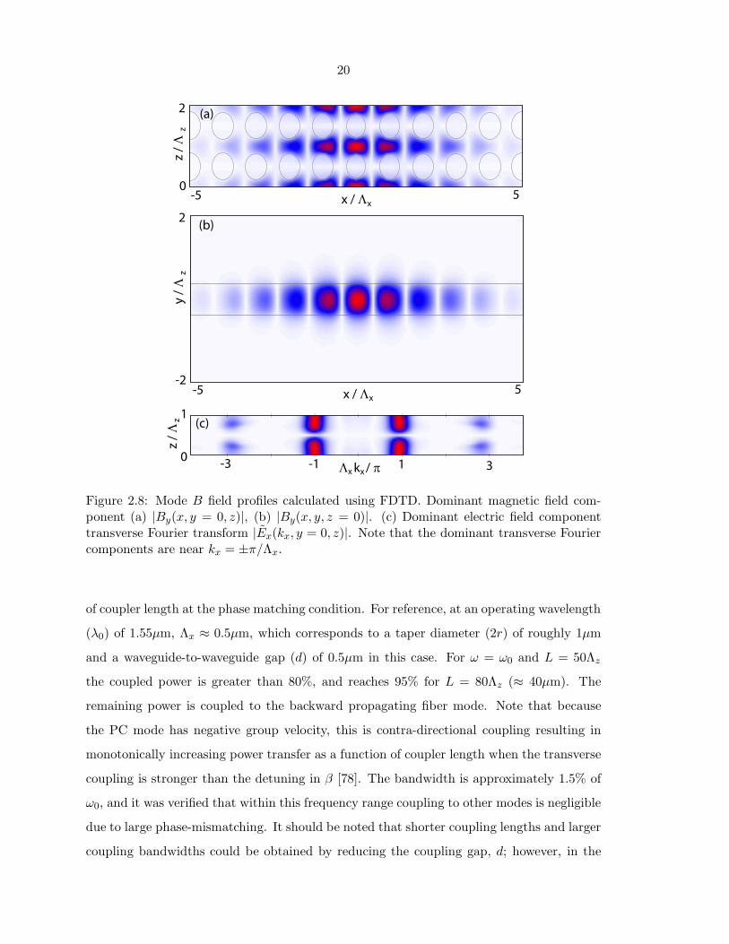
the transverse Fourier transforms of these localized modes are shown in Figs. 2.6 - 2.8. The
Fourier transforms confirm that the dominant transverse Fourier components of mode TE1
are centered about kx = 0, while those of mode B are centered about kx = ±π/Λx. Both of
these modes have negative group velocity, indicating that coupling to them from the fiber
will be contradirectional in nature.
Using the FDTD calculated fields for the PC modes, the exactly calculated fields of a

19
0 1500
1
L / Λ
|C |
2j
z
| C (0) |PC
- 2
| C (L) |PC
+ 2
| C (L) |F
+ 2
| C (0) |F
- 2
(a)
(b)
ω = ω0
L /
Λ
(ω − ω ) / ω 00
0.025
0.96
00
150
0
z
- 0.025
Figure 2.7: (a) Power coupled to PC mode TE1 from a tapered fiber with radius r = 1.15Λx
placed with a d = Λx gap above the PC as a function of detuning from phase matching andcoupler length. (b) Power coupled at ω = ω0 to the forward and backward propagating PCand fiber modes as a function of coupler length.
fiber taper, and including only those PC and fiber modes that are nearly phase-matched
(as well as their backward propagating counterparts) in the coupled mode theory, the mode
amplitudes at the coupler outputs were calculated as a function of coupler length and
detuning of ω from the phase matching frequency ω0. Figure 2.7(a) shows the resulting
coupling to mode TE1 from the fundamental mode of a taper with radius r ≈ 1.15Λx
placed d = Λx above the PC. Figure 2.7(b) shows the power in all four modes as a function
20
(a)
(b)
(c)
x / Λx5-5
z /
Λz
0
2
x / Λx5-5
y /
Λz
-2
2
Λ k / πx x-3 3
z /
Λz
0
1
-1 1
Figure 2.8: Mode B field profiles calculated using FDTD. Dominant magnetic field com-ponent (a) |By(x, y = 0, z)|, (b) |By(x, y, z = 0)|. (c) Dominant electric field componenttransverse Fourier transform |Ex(kx, y = 0, z)|. Note that the dominant transverse Fouriercomponents are near kx = ±π/Λx.
of coupler length at the phase matching condition. For reference, at an operating wavelength
(λ0) of 1.55μm, Λx ≈ 0.5μm, which corresponds to a taper diameter (2r) of roughly 1μm
and a waveguide-to-waveguide gap (d) of 0.5μm in this case. For ω = ω0 and L = 50Λz
the coupled power is greater than 80%, and reaches 95% for L = 80Λz (≈ 40μm). The
remaining power is coupled to the backward propagating fiber mode. Note that because
the PC mode has negative group velocity, this is contra-directional coupling resulting in
monotonically increasing power transfer as a function of coupler length when the transverse
coupling is stronger than the detuning in β [78]. The bandwidth is approximately 1.5% of
ω0, and it was verified that within this frequency range coupling to other modes is negligible
due to large phase-mismatching. It should be noted that shorter coupling lengths and larger
coupling bandwidths could be obtained by reducing the coupling gap, d; however, in the

21
model used here this results in stronger coupling to the backward propagating fiber mode
and a decreased asymptotic coupling efficiency. In addition, such strong coupling is best
modeled using a more complete basis within coupled mode theory or using a fully numerical
approach such as FDTD.
To illustrate the importance of a mode’s dominant transverse Fourier components for
efficient coupling, Fig. 2.9 shows the power transfer as a function of coupler length and
detuning to mode B in Fig. 2.5 from an appropriately phase matched fiber taper placed
d = Λx above the PC 1.
Although mode B is even about the mirror plane in the center of the waveguide, because
it is constructed from Bloch modes around the M -point it has relatively small amplitude
for transverse Fourier components near zero, resulting in a small transverse overlap factor
(Kij) with the fiber taper mode. This results in a coupler length ≈ 200 times longer than
that for mode TE1, as well as an extremely narrow bandwidth of ≈ 10−4% of ω0 (a property
further amplified by modeB’s low group velocity). Calculations not shown here that studied
acceptor defect modes arising from the valence band edge (M −X2) yield similar results,
despite their very broad field profiles, which would be expected to match well with the fiber.
These calculations demonstrate that by selecting a mode composed from the appropri-
ate regions in k space, efficient power transfer between a tapered fiber and the PC can be
achieved that is mode selective and that (thanks to its contradirectional character) does not
depend critically on the coupling length above some critical minimum. Using a more numer-
ically intensive supermode calculation, we now confirm that the simple coupling analysis
used above is valid.
2.4 Supermode calculations
In order to verify the coupling picture between the individual waveguide modes presented in
the previous section, it is useful to calculate the bandstructure of the hybrid fiber taper-PC
waveguide system. Because this system retains the discrete translational symmetry of the
PC waveguide, the bandstructure of its modes (the supermodes) can be calculated using
FDTD with a combination of Bloch and absorbing boundary conditions in a similar manner
1Besides the very weak coupling between this mode and the fiber taper, higher order odd slab modes maymake coupling in this region of k space impractical. Nonetheless, the calculations shown here demonstratethe importance of a mode’s transverse Fourier components.

22
L / Λ
(ω − ω ) / ω 00
0.6
00
3000
0
z
- 2.5 x 10⁻⁴ 2.5 x 10⁻⁴
Figure 2.9: Power coupled to PC mode B from a tapered fiber with radius r = 1.55Λx
placed with a d = Λx gap above the PC as a function of detuning from phase matching andcoupler length.
as the bandstructure of the isolated PC waveguide. The resulting bandstructure provides
information about the coupling between the modes of the individual waveguides. For weak
coupling, it resembles the superposition of the individual waveguide bandstructures (for
example Fig. 2.5), but with anti-crossings where the modes intersect and are coupled. The
amount of deflection at an anti-crossing is related to the strength of the coupling between the
modes, and can be used to back out physical parameters that describe the power transfer.
Figure 2.10(a) shows the bandstructure for a fiber taper of radius r = 1.17Λz = 1.46Λx
placed d = Λz = 1.25Λx above the PC waveguide studied in the previous sections. These
parameters differ slightly from those used in the previous section, but do not change the
results significantly; the larger separation results in a longer coupling length and a smaller
bandwidth, while the larger fiber radius lowers the phase matching frequency slightly. The
mirror symmetry about the y − z plane of the fiber-PC system is used to filter for modes
that are even about this plane, but the fiber breaks the mirror symmetry in the x − z
plane, and the bandstructure contains PC modes that are odd in the vertical direction, and
that are not shown in the bandstructures from the previous sections. The dispersion of the
individual fiber mode and the PC waveguide mode TE1 can be identified, and the anti-

23
_+
Fiber dispersion
Supermode dispersion
_+
(a)
(c) (d)
0.27
0.32
0.32 0.40
Λ /
λz
β Λ / 2πz
Mode TE-1
x x
y
-0.5
0
1
0
1
Figure 2.10: (a) FDTD calculated bandstructure of the full fiber taper photonic crystalsystem. The fiber taper has a radius r = 1.17Λz = 1.46Λx, and is d = Λz = 1.25Λx abovethe PC waveguide. The TE1-like and fiber-like dispersion is identified, and the symmetricand antisymmetric superpositions of these modes at the anti-crossing are labeled by the± signs. (b) The By(x, y, 0) component of the symmetric supermode. (c) The By(x, y, 0)component of the antisymmetric supermode.
crossing where they intersect indicates that the two modes are coupled. In addition, the
fundamental fiber taper mode couples strongly to a series of PC modes at higher frequencies
than mode TE1, which was not predicted from the analysis in the previous section. These
are the aforementioned second order odd (about the x− z plane) valence band TE-like PC

24
modes. These modes can be pushed to higher frequencies faster than the fundamental TE-
like modes by reducing the slab-thickness (i.e., they can be “frozen out” of the frequency
range of interest), and are typically not studied. However, their odd parity in the vertical
direction results in an electric field amplitude maxima near the PC surface, and they interact
strongly with the fiber taper. Figures 2.10(b,c) show the field profiles of the supermodes
from either side of the anti-crossing of interest. The low and high frequency supermodes
closely resemble odd and even superpositions, respectively, of the individual waveguide
modes, consistent with standard results for coupling between degenerate modes in guided
wave optics [3].
Since PC mode TE1 and the fiber mode have group velocities with opposite signs, a
bandgap is formed where they anti-cross. This is consistent with the physical picture of
the coupling: On resonance, a contradirectional coupler acts like a mirror, and reflects the
power from the forward propagating mode into the backward propagating mode. Math-
ematically, this is manifest in a non-zero imaginary part of the propagation constant, β,
inside the gap. Thus, the supermodes propagate evanescently inside the gap, and complete
contradirectional coupling is possible over a bandwidth equal to the size of the gap. The
gap at the anti-crossing of mode TE1 and the fiber mode in Fig. 2.10(a) has a width of
1% of its center frequency ω0. Coupled mode calculations similar to those of the previous
section for a fiber radius and PC-taper gap equal to those used in this section also yield a
bandwidth of 1% of ω0.
2.5 Conclusion
Using the general analysis presented in this chapter, photonic crystal waveguide modes
suitable for efficient coupling to optical fiber tapers can be identified. The photonic crystal
waveguide design presented here is predicted to allow contradirectional fiber-PC power
transfer of 95% after an 80 lattice constant (≈ 50μm) long interaction region. In the
following chapter, it will be shown that this photonic crystal waveguide can be efficiently
integrated with a photonic crystal cavity.

25
Chapter 3
Efficient fiber to cavity coupling: theoryand design
Optically accessing PC microcavities is difficult due to their ultra-small mode volume and
their external radiation pattern, which, unlike micropost [36] and Fabry-Perot [34] cavities,
is not inherently suited to coupling with conventional free-space or fiber optics. However,
the planar, chip-based nature of PC cavities lends itself naturally to integration with other
planar nanophotonic structures, such as PC waveguides [79, 80]. Initial passive studies of
PC cavities took advantage of this, and employed PC “bus” waveguides to probe the cavity
[81, 82, 83]. However, neither the coupling into the waveguide nor the waveguide-cavity
interface were designed carefully, and the total fiber to cavity coupling efficiency of these
studies was very low.
In the previous chapter, we addressed the fiber waveguide coupling problem. In this
chapter, we study how the PC waveguide can be engineered to “mode match” with the
cavity, ensuring efficient and “ideal” [84] waveguide-cavity coupling. The resulting fiber-
waveguide-cavity coupling geometery is illustrated in Figs. 3.1(a) and 3.1(b), and functions
as follows. Light is coupled evanescently from the fiber taper onto the PC chip via a PC
waveguide, where it is guided to the PC microcavity at the terminus of the PC waveguide.
Photons that are reflected from the PC cavity are then recollected into the backward prop-
agating fiber taper mode, where they are separated from the forward propagating input
signal using a fiber splitter. In this way, a single optical fiber is used to both source and
collect light from the PC microcavity.
When presented with this coupling scheme, an obvious question is whether the PC
waveguide is necessary. Can the fiber taper be efficiently coupled directly to the cavity?
Kartik Srinivasan from our group demonstrated [11] that it is possible to couple directly

26
(b)
z
ωω (β) wgω0
PCWGCavity
RT
γ ir0
Fiber taper
ηwg
γj > 0e
γ0 e
(a)
yzx
Λz = Λx Λz = 1.25 Λx
Figure 3.1: (a) Schematic of the fiber taper to PC cavity coupling scheme. The bluearrow represents the input light, some of which is coupled contradirectionally into the PCwaveguide. The green arrow represents the light reflected by the PC cavity and recollectedin the backwards propagating fiber mode. The red colored region represents the cavitymode and its radiation pattern. (b) Illustration of the fiber-PC cavity coupling process.The dashed line represents the “local” band-edge frequency of the photonic crystal alongthe waveguide axis. The step discontinuity in the bandedge at the PC waveguide - PCcavity interface is due to a jump in the longitudinal (z) lattice constant. The parabolic“potential” is a result of the longitudinal grade in hole radius of the PC cavity. Thebandwidth of the waveguide is represented by the gray shaded area. Coupling betweenthe cavity mode of interest (frequency ω0) and the mode matched PC waveguide mode(ωWG = ω0) is represented by γe
0, coupling to radiating PC waveguide modes is representedby γe
j>0, and intrinsic cavity loss is represented by γi.
between fiber tapers and PC cavities, but that because of parasitic losses from the cavity
induced by the fiber taper, this coupling is typically neither efficient nor ideal. To emphasize
the importance of ideality, we begin in Sec. 3.1 with a review of some of the key parameters
describing the loading of a general resonant structure, including coupling efficiency and
ideality, and point out specific implications for planar PC microcavities. In Sec. 3.2 we then
present a design that attempts to optimize these parameters while allowing for efficient
evanescent coupling between a fiber and the waveguide. This work was first presented in
Refs. [63] and [25].
3.1 Efficient and ideal waveguide-cavity loading
As proposed in Ref. [84] in the context of microsphere resonators, the interaction between
a PC cavity and an external PC waveguide can be described by two key parameters, the

27
coupling parameter, K, and the ideality factor, I:
K ≡ γe0
γi +∑
j �=0 γej
, (3.1)
I ≡ γe0∑
j γej
, (3.2)
where the cavity mode is characterized by its resonance frequency (ωo), its intrinsic photon
loss rate in the absence of the external PC waveguide (γi), and its coupling rates to the
fundamental TE1 mode (γe0) and higher order (including radiating) modes of the external
PC waveguide (γej>0). I describes the degree of “good” loading, via the fundamental PC
waveguide mode in this case, relative to the total loading of the resonator. K is the ratio
of “good” loading to the parasitic and intrinsic loss channels of the resonator.
The on-resonance fraction of optical power reflected by the cavity back into the PC
waveguide mode is determined by the coupling parameter, K,
Ro(ωo) =(1 −K)2
(1 +K)2. (3.3)
The remaining fractional power, 1 − Ro(ωo), is absorbed inside the PC cavity or radiated
into the parasitic output channels. The reflection resonance full-width at half-maximum
(FWHM) linewidth is given by the sum of the loss rates for all of the loss channels of the
cavity, δω = γi +∑
j γej . From Ro(ωo) and δω, the quality factor of the PC cavity mode due
to intrinsic and parasitic loss (i.e., those loss channels other than the “good” PC waveguide
TE1 channel) can be determined:
Qi+P = 2QT1
1 ±√Ro(ωo)= QT (1 +K), (3.4)
where the total loaded quality factor is QT = ωo/δω, and where the ± corresponds to the
under- and over-coupled (K ≶ 1) loading condition. On resonance, full power transfer
(critical coupling) from the “good” loading channel to the resonant PC cavity mode occurs
when K = 1.
Whereas K determines the amount of power dropped by the resonator, the role of I
is more subtle. In the case of an internal emitter, the collection efficiency (η0) of emitted

28
photons into the “good” loading channel is given by,
η0 =γe
0
γi +∑
j γej
=1
1 + 1/K, (3.5)
which depends only upon the coupling parameter K. However, the cost of obtaining a large
collection efficiency is measured by the drop in loaded quality factor of the resonant cavity
mode, which can be written in terms of K, I, and Qi as
QT
Qi= 1 − K
I(1 +K)= 1 − η0
I. (3.6)
Thus, for a given collection efficiency, to maintain a long cavity photon lifetime, I should
be maximized.
Utilizing a cavity loading method with I ∼ 1 is also important for cavity based nonlinear
optics. A simple argument can be made by studying the stored energy inside a resonant
cavity for a given input power. One can write for the on-resonance internal stored energy,
U ,
U = (1 −Ro(ωo))Qi+P
ωoPi =
4K(1 +K)2
I −K(1 − I)I
Qi
ωoPi (3.7)
where Pi is the input power in the “good” loading channel. The maximum stored energy in
the resonator occurs at Kmax = I/(2− I), giving a peak stored energy, Umax = I(Qi/ωo)Pi,
which scales directly with I.
3.2 Mode-matched cavity-waveguide design
For integrated PC cavities and waveguides, in order to maximize I it is necessary to restrict
the cavity-waveguide coupling to a single dominant waveguide mode so that γe0 � γe
j>0.
Parasitic waveguide modes with cavity coupling rates γej>0 may come from a number of
sources: (i) radiation modes above the light cone of the PC slab, (ii) bulk PC slab modes
that are not laterally confined, and (iii) other laterally confined PC slab modes. In order
to effectively load the cavity with the waveguide so that I ∼ 1, the cavity mode of interest
must radiate preferentially into a single waveguide mode1. To satisfy this criteria, the design
1Note that a single guided -mode PC waveguide (i.e., a waveguide mode in a full in-plane photonicbandgap) does not guarantee efficient waveguide-cavity coupling, as the cavity mode may still couple radiateinto leaky modes of the PC waveguide.

29
described in this chapter has two important features: (i) the waveguide and cavity modes
of interest have similar transverse field profiles (see Fig. 3.2), which allows the cavity to be
efficiently loaded end-on, and (ii) the end-fire PC waveguide-cavity geometry restricts the
cavity to a single output channel, in a manner analogous to a Fabry-Perot cavity with a
high reflectivity back mirror and a lower reflectivity front mirror2.
The PC cavity that we wanted to out-couple with a PC waveguide was studied in Ref.
[76]. There, Srinivasan, et al. used a group theoretical analysis to design a cavity in a square
lattice PC slab that supports a high-Q (≈ 105) donor defect mode, whose FDTD calculated
field profile is shown in Figs. 3.2(a,b). The defect cavity was formed by introducing a donor
defect with C2v symmetry in the form of a parabolic grading of the hole radius in both in-
plane directions (the x- and z-directions, as depicted in Figure 3.2(a)). Since the first order
bandgap energy minima of the conduction band in a square lattice occur at the X1,2 points
of the IBZ, donor modes from this band are expected to be composed of Fourier components
in a neighborhood of the ±kX1 and ±kX2 points in k space. The high-Q mode transforms
as the A2 representation of the C2v [76], and its dominant k-space components result in a
highly directional mode profile along the z-direction, parallel to the Γ−X1 direction of the
reciprocal lattice. In anticipation of integration with this cavity, the waveguide studied in
Ch. 2 shares an identical grade in hole radius as that in the x-direction of the defect cavity.
The resultant similarity in the lateral (x-direction) mode profile of the A2 cavity and TE1
waveguide modes is clear from the field plots in Fig. 3.2. The lateral overlap factor of these
two modes is |〈BWGy |BCav
y 〉xy| ∼ 0.98, where the waveguide and cavity fields are evaluated at
their anti-nodes in the z-direction. This near unity modal overlap suggests that the cavity
mode will radiate dominantely into the TE1 mode, i.e., I ∼ 1.
Because of the similarity between the lateral grade in the hole radius of the PC in
the waveguide and cavity sections, the coupled waveguide-cavity illustrated in Fig. 3.1
can be approximately viewed as a one dimensional system along the z-direction. This
simplified picture is schematically represented in Fig. 3.1(b), where the frequency of the
(local) fundamental “waveguide” mode is plotted versus z for a fixed lateral grading in the
PC hole radius. A buffer region consisting of a variable number of periods of the square
photonic lattice is placed between the end of the waveguide and the defect cavity. As
2This is in contrast to side-coupled [10], in-line [82], and direct taper coupled [11] geometries, in whichthe cavity radiates equally into backward and forward propagating waveguide modes (bounding K ≤ 1 andI ≤ 0.5)

30
(b)(a)
(d)(c)
y
y
x
x
x
z
z
Figure 3.2: (a,b) High-Q defect cavity mode profiles. Plots of the magnetic field pattern areshown in (a) the x− z plane (|By(x, y = 0, z)|), and (b) the x− y plane (|By(x, y, z = 0)|).(c,d) PC waveguide TE1 mode field profiles, taken in the (a) the x − z plane and (b) thex− y plane.
illustrated schematically in Figure 3.1(b), light tunnels between the cavity and waveguide
through the barrier. In general, the efficiency and strength of coupling between the cavity
and waveguide are tuned by: (i) adjusting the compression and/or the filling fraction of
the waveguide lattice so that the TE1 waveguide mode is resonant with the cavity mode,
and (ii) tailoring the waveguide defect so that the waveguide and cavity modes have similar
transverse field profiles. The frequency of the lateral guided mode is tuned at different
positions in z by adjusting the nominal hole radius (lattice filling fraction) and/or the lattice
constant in the z-direction (lattice compression/stretching). The mode’s dispersion in the

31
PC waveguide section results in a finite frequency bandwidth and is represented in the figure
by a shaded region. So as to avoid stitching different lattices, the lateral lattice constant is
kept constant (Λcavx = ΛWG
x ). In this way, we can engineer band-offsets to produce tunneling
barriers and create localized resonant cavities along the z-direction. In order to couple from
the waveguide to the cavity, the waveguide mode must be in resonance with the localized
cavity mode. For the waveguide and cavity mode system considered here, this degeneracy is
achieved by adjusting the waveguide lattice compression ΛWGx /ΛWG
z . Additionally, for the
designs studied here there is no discontinuity in the hole size, so that the strength of the
coupling between the resonant cavity and waveguide modes is determined by the band-offset
due to the lattice compression of the waveguide (height of the barrier) and the number of
buffer periods between the waveguide and cavity sections (width of the barrier).
An analysis of the coupling between the waveguide the cavity was performed using a
2D effective index FDTD simulation of the full cavity-waveguide system. Although these
2D simulations neglect vertical radiation loss, this analysis can determine how effectively
the lateral profile of the waveguide mode has been matched to that of the cavity mode, a
major consideration in our waveguide design and a necessity for efficient waveguide-cavity
coupling as discussed above. Figure 3.3 shows the cavity mode in the presence of a series of
waveguides with different lattice compressions. The magnetic field is shown at instants in
time when it is a maximum (confined) and a minimum (radiating) in the cavity. Coupling to
the TE1 waveguide is negligible when the lattice is uncompressed, since its lowest frequency
(which occurs at the X point) is higher than the cavity mode frequency. In this case the
cavity radiates as if it were unloaded and its dominant in-plane radiation is in the kM
directions. When the lattice is compressed, the waveguide mode frequencies are lowered,
and the cavity becomes resonant with the TE1 waveguide mode labeled by some propagation
constant, β (see Fig. 3.1(b)). The loaded cavity couples to the TE1 waveguide mode, but
not into other (degenerate in ω but detuned in β) parasitic waveguide modes. As discussed
above, this mode-selective coupling does not rely on a full photonic bandgap and is due to the
similarity between the transverse profiles of the cavity and waveguide modes of interest. The
simulations also show that because of the TE1 dispersion and its corresponding frequency
bandwidth, the waveguide-cavity coupling does not depend critically on the amount of
lattice compression, so long as the compression is sufficient to lower the frequency at the X
point of the TE1 mode below the cavity mode frequency. By tuning the lattice compression

32
(a)
(b)
(c)
Figure 3.3: Coupling from the defect cavity to the PC waveguide for varying waveguidelattice compression at instances in time when the cavity magnetic field is a minimum (left)and a maximum (right). The envelope modulating the waveguide field is a standing wavecaused by interference with reflections from the boundary of the computational domain. Thediagonal radiation pattern of the cavity is due to coupling to the square lattice M points,and is sufficiently small to ensure a cavity Q of ≈ 105. |B| for (a) ΛWG
x /ΛWGz = 20/20 (b)
ΛWGx /ΛWG
z = 20/25 (ratio used in the previous section) (c) ΛWGx /ΛWG
z = 20/29.
beyond this minimum, the propagation constant (and group velocity) of the TE1 mode
when it is resonant with the cavity mode is adjusted. By choosing the compression such
that this propagation constant phase matches with a fiber taper (Λx/Λz = 20/25 for the
case considered in the previous section), an efficient fiber-taper/PC-waveguide/PC-cavity
probe is theoretically realized.
3.3 Conclusion
The fiber-waveguide-cavity coupling technique studied in this chapter provides highly effi-
cient fiber to PC cavity coupling. By designing the PC waveguide so that it is mode-matched
with the PC cavity, nearly ideal loading of the cavity by the waveguide is possible, ensuring
that the cavity-Q is not degraded by parasitic waveguide loss. The resulting fiber-to-cavity

33
coupling channel can be used to study nonlinear effects within the PC cavity for low fiber
input power, as shown in Ch. 5, and will also be useful as an efficient photon collector in
future single photon source experiments using PC cavities.

34
Chapter 4
Probing photonic crystals with fibertapers: experiment
In this chapter, the evanescent coupling scheme described theoretically in Ch. 2 and Ch.
3 is demonstrated experimentally. It is shown that in addition to providing efficient fiber-
to-chip coupling, a fiber taper can be used as a wafer-scale probe to study the spectral
and spatial properties of the optical modes supported by photonic crystal devices. By
circumventing the intrinsic spatial and refractive index mismatch between optical fiber and
PC devices, and taking advantage of the strong dispersion and undercut geometry inherent
to PC membrane structures, efficient power transfer and rapid characterization of optical
modes of a PC waveguide using fiber tapers are possible. This tool significantly simplifies
and accelerates the design and fabrication cycle that must often be iterated in order to
realize high quality nanophotonic elements, and provides an interface between wavelength
scale nanophotonic circuits and fiber optics.
This work was originally presented in Refs. [48, 47, 25]. Section 4.2 presents experimental
results demonstrating that the coherent interaction over the length of the coupling region
between phase matched modes of a fiber taper and Si photonic crystal waveguide manifests
in 97% power transfer. In Sec. 4.3, the fiber taper is used to probe the dispersive and spatial
properties of Si PC waveguide modes. These techniques are then leveraged in Sec. 4.4 to
achieve high coupling efficiency (> 44%) from a fiber taper into a Si PC microcavity that
is integrated with a photonic crystal waveguide.

35
(a)
(b)
Fiber taper mount
PC chip
Fiber taper
PCWG
z
y
xFigure 4.1: Schematic of the coupling scheme. (a) Illustration of the fiber taper in the “U-mount” configuration that is employed during taper probing of the PC chip. (b) Illustrationof the fiber taper positioned in the near field of the PC waveguide, and the contra-directionalcoupling between waveguide that occurs on-resonance.
4.1 Experimental details
The optical coupling scheme used in this work is shown schematically in Fig. 4.1. An optical
fiber taper, formed by heating and stretching a standard single-mode silica fiber, is placed
above and parallel to a PC waveguide. The fiber diameter changes continuously along the
length of the fiber taper, reaching a minimum diameter on the order of the wavelength
of light. Light that is initially launched into the core-guided fundamental mode of the
optical fiber is adiabatically converted in the taper region of the fiber into the fundamental
air-guided mode, allowing the evanescent tail of the optical field to interact with the PC
waveguide; coupling occurs to phase-matched PC waveguide modes that share a similar
momentum component down the waveguide at the frequency of interest. The undercut
geometry of the PC waveguide prevents the fiber taper from radiating into the PC substrate.

36
4.1.1 Fiber taper fabrication
The fiber tapers are fabricated by simultaneously heating and stretching a standard single
mode fiber until the minimum diameter of the fiber is on the order of a wavelength. A
detailed description of the apparatus and fabrication is given by M. Borselli’s thesis [85];
what follows is a brief outline. Detailed descriptions of the theory of fiber taper formation
can be found in Refs. [40, 41].
A standard single mode fiber designed for operation at the wavelength of interest (SMF
28 for operation at 1550 nm, Nufern 780HP for operation at 852 nm, etc.) is stripped of its
protective acrylate cover over a 1 cm length. This stripped region is then placed between
two magnetic fiber clamps, each of which is attached to a computer controlled single axis
linear translation stage. Care is taken to ensure that the clamped section of fiber is well
tensioned, and that the clamps do not impart any torque. A hydrogen torch flowing a small
amount of H2 is ignited, resulting in a gentle flame. The torch is mounted on a computer
controlled single axis linear translation stage (Suruga Seiki), which controls the separation
between the torch and the fiber in the direction perpendicular to the fiber. A manual three
axis micrometer attaches the torch to the translation stage, and is used to fine tune the
position of the flame.
Using a LabView program, the stages holding the fiber are commanded to begin moving
in opposite directions at a constant speed of 1-2 μm/s, further tensioning the fiber. Simul-
taneously, the stage holding the H2 flame is quickly moved to position the flame directly
below the tensioned fiber. The flame heats the fiber above the glass softening point, allow-
ing it to be stretched by the continuously moving stages holding the fiber. As the fiber is
stretched, its diameter shrinks (by conservation of volume).
During this process, the optical transmission through the fiber is monitored by coupling
a laser source to one end of the fiber and monitoring the output of the other end with
a photodetector. As the minimum fiber diameter shrinks, the tapered region of the fiber
transitions from being single-mode to multimode, often resulting in oscillations in the fiber
transmission as a function of pull length due to coupling and interference between the
fundamental mode and higher order modes within the fiber. However, as the minimum
fiber diameter shrinks below a wavelength, the fiber becomes single-mode once again, and
37
the transmission becomes independent of pull length1. This “feature” in the transmission
as a function of pull time can be used to calibrate the size of the fiber taper in situ.
Once the fiber taper has reached the desired minimum diameter (usually between 0.5
μm and 1.5 μm, after ∼ 10-15 mm of pulling) the computer control halts the movement
of the stages holding the fiber, and moves the stage positioning the H2 flame away from
the fiber. The mounts holding the fiber are then released, and the tapered fiber can then
be picked up manually. Despite its small minimum diameter, the tapered region is strong
enough to support the weight of a 1m long fiber tail. The fiber taper is then manually
bent into a “U” shape, before being attached to a flat holder (with specially machined
grooves) using adhesive tape, as illustrated in Fig. 4.1(a). Putting the fiber in a “U” shape
is easily achieved by holding the two fiber tails in one hand, usually by pinching both fiber
tails between the thumb and index finger. The tapered region then naturally takes on the
desired “U” geometry. The fiber can then be spliced into the experimental setup, and is
ready to be used for coupling to PC devices. As long as the taper is adiabatic (compared
to the wavelength of light), the overall insertion loss in the fiber at the end of the pull can
be extremely low, and is typically below 10%.
As discussed in Sec. 4.2, the fiber tapers fabricated as described above can only be used
to probe one-dimensional arrays of devices. Recently our group [45] as well as groups in
Korea [86], and Australia [87], have developed “dimpled” fiber tapers, which require an
additional local heating step after the initial taper formation to create local curvature in
the otherwise straight fiber taper, allowing the taper to be used to probe two-dimensional
arrays of devices. These tapers are not used in the results presented here however.
4.1.2 Fiber probing measurement apparatus
The measurement apparatus necessary for fiber taper probing of PC devices is very sim-
ple. The “U”-mounted fiber taper [Fig. 4.1(a)] is attached to a three-axis stage that has
manual micrometer control in the horizontal axes and a computer controlled 50 nm res-
olution motorized stepper in the vertical axis. The sample is mounted on a micrometer
controlled goniometer (for tip-tilt adjustment) attached to a rotation stage, which in-turn
is attached to a two horizontal axis computer controlled 50 nm resolution motorized stepper
1An air clad fiber with refractive index nf is single mode if its diameter d < 2.405λ/π�
n2f − 1 [3]. For
glass, nf = 1.45, requiring d < 0.73λ.

38
r1
κ κ' κ't
r2
t'
t'
R
TFiber taper
PCWG
DT
Laser
DR
3dB
z = 0 z = L
Polarizer
Figure 4.2: Illustration of the optical path within the fiber optic measurement apparatus.DT and DR represent photodetectors used to measure the transmitted and reflected signalsrespectively.
stage. This allows the fiber taper to be accurately positioned at varying heights and lateral
displacements relative to individual PC devices, as in Fig. 4.1(b).
All of the optics used in the results presented in this chapter are fiber based. A schematic
detailing the optical path within the fiber and PC device is shown in Figure 4.2. To spec-
trally characterize the taper-PC waveguide coupler, an external cavity swept wavelength
source (New Focus “Vidia”) with wavelength range 1565-1625 nm was connected to the
fiber taper input via a polarizer and a 3dB coupler. At the fiber taper output, a photode-
tector (DT) was connected to measure the transmitted power past the taper-PC interaction
region. An additional photodetector (DR) was connected to the second 3dB coupler input
to measure the light reflected by the PC interaction region.
4.1.3 Photonic crystal fabrication
A typical fabricated array of PC waveguides is shown in Fig. 4.3. These PC devices were
fabricated from a silicon-on-insulator (SOI) wafer purchased from Soitec. The Si thickness
was 340 nm, and the underlying oxide was 2 μm thick. Arrays of PC devices are defined

39
using electron beam lithography and other semiconductor processing techniques, details of
which are given here and in K. Srinivasan’s thesis [88].
Samples are first spin coated with a thin layer of ZEP-520 (Zeon Corporation, Japan)
electron beam resist (5000 RPM for 60 seconds, followed by a 20 minute 180oC bake).
Electron beamwriting is used to create etch masks on the SOI wafer from the electron beam
resist. The etch masks are defined using AutoCAD generated pattern files that are read by a
computer program called “Bewitch” written by Oliver Dial, a former Caltech undergraduate
student. Bewitch converts the AutoCAD .dxf file into a raster pattern that is output to
a Hitachi S-4300 cold field emission scanning electron microscope (SEM) in the form of a
set of two voltages that control the SEM x and y scan coils. The raster rate is determined
by the desired electron dose per pixel; for doses between 30-60 μC/cm2, speeds ranging
from 10-250 kHz are typical, depending on the pixel size and electron beamcurrent. For the
photonic crystals fabricated here, low beamcurrent (5 pA), low speed (35 kHz) beamwrites
were used, with the SEM accelerating voltage set at 15 kV and the SEM magnification
between 450X-1000X. This beamwriting system does not have stitching capabilities, and the
maximum pattern size is limited by the field of view of the SEM at the desired beamwriting
magnification (up to ∼ 100μm × 100μm). Arrays of patterns are written by moving the
stage after a pattern is complete, and repeating the beamwrite. Often, within an array
of masks employing identical input beamwriting patterns, both the lattice constant and
nominal hole radius are varied by adjusting the “scaling” of the Bewitch output voltages,
and the beamwriting speed (dwell time per pixel), respectively. “Proximity effects”, in which
the post-beamwrite hole size deviates from the desired size due to exposure of neighboring
holes, are compensated for a priori in the pattern files.
For the beamwrite, it is crucial that the sample surface is level along the axis of the
stage movement so that the electron beam remains focused on the surface for the entire
beamwrite. In practice, the SEM sample mount surface has a slight tilt. This sample mount
consists of a 2 cm diameter aluminum sample holder that is screwed into a chuck that, in
turn, is interfaced with the SEM positioning stage. By rotating the position of the top
sample holder surface (by adjusting how far it is screwed into the chuck), the tilt axis can
be rotated relative to the beamwriting stage movement axis. At a unique position, these
axes are aligned, and the height of the sample surface at the beam position does not change
when the sample stage is moved along a desired axis. This setting can be determined by

40
isolationetch
PCWG
fiber taper
50 μm
5 μm
Figure 4.3: SEM image of a fabricated photonic crystal array. One of the devices is posi-tioned below a fiber taper. Also visible is the edge of the “isolation” mesa on which the PCarray is defined.
trial and error, checking each new setting by imaging an array of devices and confirming
that the SEM focus does not need to be adjusted when the sample is moved along the axis
of interest. Once the setting has been determined, it is important to never inadvertently
adjust the sample holder, and to be consistent with the orientation of the sample on the
holder. A better long term solution would be to have a custom sample holder, with a top
flat surface, machined to our specifications.
After the beamwrite, a SF6/C4F8 based inductively coupled plasma reactive ion etching
(ICP-RIE) is used to selectively remove Si material not covered by the ZEP mask. The
ratio of SF6 to C4F8 was optimized to provide smooth and vertical sidewalls; too much
SF6 results in roughness, while too much C4F8 results in angled sidewalls. After this dry
etch, the remaining ZEP is removed using acetone or an acidic H2SO4:H2O2 “Piranha”
cleaning step. Photolithography is then used to cover the etched patterned regions with
a photoresist mask (Shipley 5214); and a SF6 isolation etch, > 10 μm in depth, is per-

41
formed to remove unpatterned material surrounding the PC devices (Fig. 4.3). This step
ensures that the fiber taper only evanescently interacts with the PC regions, and not with
the surrounding unpatterned material. The suspended membrane structure is created by
selectively removing the underlying silicon dioxide layer using a hydrofluoric acid wet etch
for approximately three minutes at room temperature. In some cases, a short ICP-RIE etch
is used to uniformly thin the top Si layer, depending on the Si thickness required by the
device design. Finally, a H2SO4:H2O2 cleaning step is used to remove any organic material
(such as ZEP) on the device surface.
4.2 Efficiently coupling into photonic crystal waveguides
Using the fabrication techniques described above, and the design presented in Ch. 2, PC
waveguides were formed in a 300 nm thick Si membrane by introducing a grade in hole radius
along the transverse direction of a compressed square lattice of air holes, as shown by Figure
4.4(a-b). As described in Ch. 2, the coupling of interest for this PC waveguide design occurs
between the fundamental linearly polarized fiber mode and the TE1 PC waveguide mode,
whose field profile is shown in Fig. 4.4(a) and dispersion is shown in Fig. 4.4(c). This PC
waveguide mode has a negative group velocity, resulting in contradirectional coupling, as
depicted in Fig. 4.1(b) and Fig. 4.2.
Although the coupling efficiency of this technique can be inferred by analyzing the signal
transmitted through the fiber taper as a function of wavelength and fiber taper position,
a more direct measurement is to study the power coupled into and then back out of a PC
waveguide. This measurement allows a lower bound for the input-output coupling efficiency
to be absolutely established. In this section, by studying light that is coupled into a PC
waveguide, reflected by an end-mirror at the PC waveguide termination, and then coupled
into the backward propagating fiber mode, as depicted in Fig. 4.2, it is shown that the
coupling has near unity efficiency.
In initial studies of evanescent coupling to such PC waveguides [46], the waveguide
termination consisted of a 2 μm region of undercut Si, followed by an 8 μm length of
non-undercut SOI and a final air interface. The interference from multiple reflections at the
three interfaces within the waveguide termination resulted in a highly wavelength dependent
reflection coefficient, making quantitative analysis of signals reflected by the PC waveguide
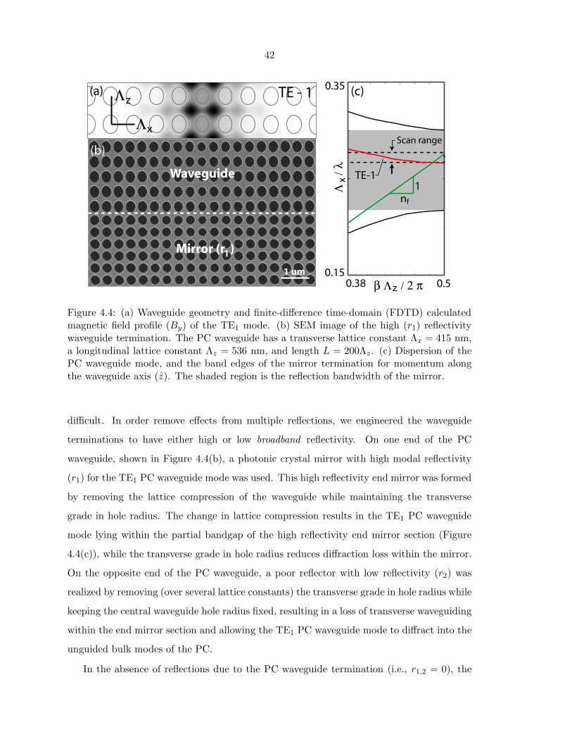
42
Mirror (r )
Waveguide
1
TE - 1
Λx
Λz(a)
(b)
1 um
nf
1
0.50.380.15
0.35
β Λ / 2 πz
Λ
/ λx
(c)
TE-1
Scan range
Figure 4.4: (a) Waveguide geometry and finite-difference time-domain (FDTD) calculatedmagnetic field profile (By) of the TE1 mode. (b) SEM image of the high (r1) reflectivitywaveguide termination. The PC waveguide has a transverse lattice constant Λx = 415 nm,a longitudinal lattice constant Λz = 536 nm, and length L = 200Λz . (c) Dispersion of thePC waveguide mode, and the band edges of the mirror termination for momentum alongthe waveguide axis (z). The shaded region is the reflection bandwidth of the mirror.
difficult. In order remove effects from multiple reflections, we engineered the waveguide
terminations to have either high or low broadband reflectivity. On one end of the PC
waveguide, shown in Figure 4.4(b), a photonic crystal mirror with high modal reflectivity
(r1) for the TE1 PC waveguide mode was used. This high reflectivity end mirror was formed
by removing the lattice compression of the waveguide while maintaining the transverse
grade in hole radius. The change in lattice compression results in the TE1 PC waveguide
mode lying within the partial bandgap of the high reflectivity end mirror section (Figure
4.4(c)), while the transverse grade in hole radius reduces diffraction loss within the mirror.
On the opposite end of the PC waveguide, a poor reflector with low reflectivity (r2) was
realized by removing (over several lattice constants) the transverse grade in hole radius while
keeping the central waveguide hole radius fixed, resulting in a loss of transverse waveguiding
within the end mirror section and allowing the TE1 PC waveguide mode to diffract into the
unguided bulk modes of the PC.
In the absence of reflections due to the PC waveguide termination (i.e., r1,2 = 0), the

43
fiber-PC waveguide junction can be characterized by
⎡⎣ a+
F (L)
a−PC(0)
⎤⎦ =
⎡⎣ t κ′
κ t′
⎤⎦⎡⎣ a+
F (0)
a−PC(L)
⎤⎦ , (4.1)
where κ and κ′ are coupling coefficients, t and t′ are transmission coefficients, and a+F (z) and
a−PC(z) are the amplitudes of the forward propagating fundamental fiber taper mode and the
backward propagating TE1 PC waveguide mode, respectively. The coupling region extends
along the z-axis, with z = 0 corresponding to the input and z = L to the output of the
coupler. As illustrated by Figure 4.2, non-zero r1,2 introduce feedback into the system. This
allows input light coupled from the forward propagating fundamental fiber taper mode into
the TE1 PC waveguide mode to be partially reflected by the PC waveguide termination, and
subsequently coupled to the backward propagating fundamental fiber taper mode. In the
presence of this feedback within the PC waveguide, the normalized reflected and transmitted
powers in the fiber taper are given by [89]
T =∣∣a+
F (L)∣∣2 =
∣∣∣∣t+κκ′t′r1r2
1 − r1t′r2t′
∣∣∣∣2
, (4.2)
R =∣∣a−F (0)
∣∣2 =∣∣∣∣ κκ′r11 − r1t′r2t′
∣∣∣∣2
, (4.3)
for a+F (0) = 1 and a−PC(L) = 0. By measuring T and R, and considering Eqs. (4.2) and
(4.3), we can determine the efficiency of the fiber-PC waveguide coupling as measured by
|κκ′|.
In the measurements presented here, a fiber taper with 2 μm diameter was used to probe
the PC waveguide of Figure 4.4(b). Figures 4.5(a) and 4.5(b) show T and R as a function
of wavelength when the taper is aligned with the PC waveguide at a height of g = 0.20
μm, and indicate that the phase-matched wavelength is λ ∼ 1598 ± 5 nm. Data for T is
normalized by the taper transmission when it is not interacting with the device. Asymmetry
in the fiber taper loss about the coupling region was taken into account by repeating the
measurements with the direction of propagation through the taper and the orientation of the
PC waveguide sample reversed; the geometric mean of the values for R obtained from the
two orientations takes any asymmetry into account. As described in Section 4.3, coupling

44
to the guided TE1 mode of the PC waveguide was confirmed by studying the coupling
dependence upon polarization, lateral taper displacement, and fiber taper diameter. Figure
4.5(c) shows T and R at the resonant wavelength of the PC waveguide nearest the phase-
matching condition [the minima and maxima in T (λ) and R(λ)], as a function of taper
height, g, above the PC waveguide. Included in Figure 4.5(c) is the off-resonant (away from
phase-matching) transmission, T off, through the fiber. A maximum normalized reflected
power Rmax ∼ 0.88 was measured at a height of g ∼ 0.25 μm, where the corresponding
transmission was T < 0.01. As can be seen in the wavelength scans of Figure 4.5(a), at this
taper height the Fabry-Perot resonances due to multiple reflections from the end mirrors
of the PC waveguide are suppressed for wavelengths within the coupler bandwidth due to
strong coupling to the fiber taper. Ignoring for the moment the effects of multiple reflections
in Eq. 4.3, the maximum optical power coupling efficiency is then |κκ′| =√Rmax/|r1|, where
the square root dependence upon Rmax is a result of the light passing through the coupler
twice in returning to the backward propagating fiber mode. Assuming the high reflectivity
mirror is perfect (unity reflection), for the measured Rmax = 0.88 this implies 94% coupling
of optical power from taper to PC waveguide (and vice-versa).
By further comparison of T (g) and R(g) with the model given above, this time including
feedback within the PC waveguide, we find that the high reflectivity PC waveguide end-
mirror is imperfect and that Rmax is in fact limited by mirror reflectivity, not the efficiency
of the coupling junction. For this comparison, we take the elements of the coupling matrix to
satisfy the relations |t|2 + |κ|2 = 1, κ′ = κ, and t′ = t∗ of an ideal (lossless) coupling junction
[89]. For the phase matched contradirectional coupling considered here, the dependence of
κ on g can be approximated by |κ(g)| = tanh [κ⊥,0 exp(−g/g0)L] [78], where κ⊥,0 and g0
are constants. Substituting these relations into Eqs. (4.2) and (4.3), T and R can be fit
to the experimental data with r1,2, κ⊥,0 and g0 as free parameters2. Note that waveguide
loss can also be included in the model; however, it is found to be small compared to the
mirror loss. Figure 4.5(c) shows the fits to the data for g ≥ 0.20 μm; for g < 0.20 μm non-
resonant scattering loss is no longer negligible and the ideal coupling junction model breaks
down. Note that the off-resonant scattering loss is observed to effect the reflected signal at
a smaller taper-PC waveguide gap than for the transmitted signal, indicating that within
the coupler bandwidth 1 − T off is an overestimate of the amount of power scattered into
2We take r1t′r2t
′/|r1t′r2t
′| = 1, corresponding to a resonant condition within the PC waveguide..

45
0 10.5 1.50
0.6
0.4
0.2
1
0.8
0
0.6
0.4
0.2
1
0.8
Taper height g (um)
No
rmal
ized
refle
ctio
n
1565 16251565 1625
(b)(a)
(c)
No
rmal
ized
tra
nsm
issi
on
transmission (T)reflection (R)Toff resonance
|κ|2
Wavelength (nm) Wavelength (nm)
0
0
1
2
|r | = 0.90|r | = 0.52g = 0.28 umκ L = 5.58
2
2
Figure 4.5: (a) Reflection and (b) transmission of the fiber taper as a function of wavelengthfor a taper height of 0.20 μm. Both signals were normalized to the taper transmission withthe PC waveguide absent. (c) Measured taper transmission minimum, reflection maximum,and off-resonant transmission as a function of taper height. Also shown are fits to the data,and the resulting predicted coupler efficiency, |κ|2.
radiation modes. From the fits in Figure 4.5(c), the PC waveguide end-mirror reflectivities
are estimated to be |r1|2 = 0.90 and |r2|2 = 0.52, and the optical power coupling efficiency
(|κ|2) occurring at Rmax (g = 0.25 μm) is approximately 97%.
4.3 Real- and k-space waveguide probing
In this section, we demonstrate that by utilizing the micron-scale lateral size and the dis-
persion of the fiber taper, the evanescent coupling technique can be used for mapping the
bandstructure and spatial profile of PC waveguide modes. A device similar to that studied
in Sec. 4.2 is characterized in this section, but with two important differences: (i) It does

46
not have a high reflectivity end mirror, and (ii) the Si slab thickness is varied from 340 nm
to 300 nm during the testing, in order to study the dispersive properties of the waveguide
modes, as described below.
4.3.1 Bandstructure mapping
Figure 4.6(a) shows an approximate bandstructure of the TE-like modes of the host com-
pressed square lattice PC slab whose dominant Fourier components are in the direction of
the waveguide, and that will consequently couple most strongly with the fundamental fiber
taper mode. Superimposed upon this bandstructure are the important donor -type defect
waveguide modes. In addition to the dispersion of the TE1 mode studied in Sec. 4.2, which
has a negative group velocity and originates from the conduction band edge, the dispersion
of a defect mode labeled TE2, which has positive group velocity and originates from the
second order (in the vertical direction) valence band-edge, is shown. A typical fiber taper
dispersion curve is also shown, lying between the air and silica light lines.
In Figure 4.7(a-b), 3D FDTD simulations were used to accurately calculate the PC
waveguide bandstructure in the regions where phase-matching to the fiber taper is expected
to occur. The FDTD-calculated in-plane magnetic field profiles of the TE1 and TE2 PC
waveguide modes (taken in the mid-plane of the dielectric slab) near their respective phase-
matching points are shown in Figs. 4.6(b,c). Although one can couple to either of the TE1 or
TE2 modes, the TE1 mode is of primary interest here because of its fundamental nature in
the vertical direction and its similar properties to that of the high-Q cavity mode discussed
in Ch. 2.
In order to probe the bandstructure of the PC waveguide, the transmitted power through
the fiber taper was monitored as a function of wavelength, taper position relative to the
PC waveguide, and taper diameter. By varying the position along the fiber taper of the
interaction region between the PC waveguide and taper (as measured by lc, the distance
from the fiber taper diameter minimum), the diameter (d) of the fiber taper, and hence the
propagation constant (β) of the fiber taper mode interacting with the PC waveguide mode,
could be tuned. Tuning from just below the air light-line (d = 0.6 μm, neff = βc/ω ∼ 1.05),
to just above the silica light-line (d = 4.0 μm, neff ∼ 1.40) was possible. Figure 4.7(c) shows
the taper transmission as a function of wavelength and sample position (lc) when the taper
is centered above the PC waveguide at a height g ∼ 700 nm from the PC waveguide surface.

47
TE - 1TE - 2Taper
0 0.5β Λ / 2 πz
Λ /
λz
0
0.5 (a)
1
nair
nsilica
1
TE - 1
TE - 2
Λx
Λz(b)
(c)
Figure 4.6: (a) Approximate bandstructure of the PC waveguide studied in Sec. 4.3. Onlythe TE-like modes that couple most strongly with the fiber taper are shown. The dispersionof a typical fiber taper is also indicated. (b) FDTD calculated magnetic field profile for theTE1 mode, taken in the mid-plane of the dielectric slab. (c) Same as (b), but for the TE2
mode.
Resonances corresponding to both the TE1 counter- and TE2 co-propagating modes can be
identified. SEM measurements of the taper diameter as a function of position (lc) were used
to calculate the propagation constant of each resonance, allowing the PC waveguide modes’
dispersion to be plotted [Fig. 4.7(e)]. The measured bandstructure is in close agreement
with the FDTD calculated dispersion of Fig. 4.7(a), replicating both the negative group
velocity of the TE1 mode and the anti-crossing behavior of the odd vertical parity TE2 and
TM1 modes. Figures 4.7(d,f) show analogous data obtained by probing the sample after
the Si slab thickness, tg, has been thinned using a short ICP-RIE dry etch to better isolate
the TE1 mode in ω−β space. As predicted by the FDTD simulation (Fig. 4.7(b)), the TE1
mode is seen to shift slightly higher in frequency due to the sample thinning, whereas the
higher-order TE2 mode shifts more quickly with slab thickness and is effectively “frozen”
out of the laser scan range.
As in Sec. 4.2, the dependence of the waveguide power transfer on coupling strength,

48
increasing fiber radius
λ (n
m)
0.32 0.44 0.32 0.44
l (mm) l (mm)0 1.5 0 4.5
β Λ / 2 πz β Λ / 2 πz
increasing fiber radius
Λ /
λz
1565
1625
0.30
0.31
c c
(c)
(e)
(d)
(f)
t / Λ = 0.85g x t / Λ = 0.75g x
0.32 0.44 0.32 0.44β Λ / 2 πz β Λ / 2 πz
Λ /
λz
0.28
0.36 (b)(a)1
nair
1
nsilica
Figure 4.7: 3D FDTD calculated dispersion of the TE1 (dotted line), TE2 (dashed line),and TM1 (dot-dashed line) modes for the (a) un-thinned (tg = 340 nm), and (b) thinned(tg = 300 nm) graded lattice PC waveguide membrane structure (nSi = 3.4). Measuredtransmission through the fiber taper as a function of wavelength and position along thetapered fiber for (c) un-thinned sample and (d) thinned sample (different tapers were usedfor the thinned and un-thinned samples, so the transmission versus lc data cannot be com-pared directly). Transmission minimum (phase-matched point) for each mode in the (e)un-thinned and (f) thinned sample as a function of propagation constant. In (a-b), thelightly shaded regions correspond to the tuning range of the laser source used.
and the overall efficiency of the coupling process were studied by varying the gap between
the fiber taper and PC waveguide. Figure 4.8(a) shows the transmission through the fiber
taper, with the coupling region occurring at a taper diameter of d = 1.9 μm for varying
taper heights above the thinned PC waveguide. Figure 4.8(b) shows the same measurement,
but with the coupling region occurring at a taper diameter of d = 1.0 μm, and for a PC
waveguide with slightly smaller nominal hole size. In both cases, the central resonance
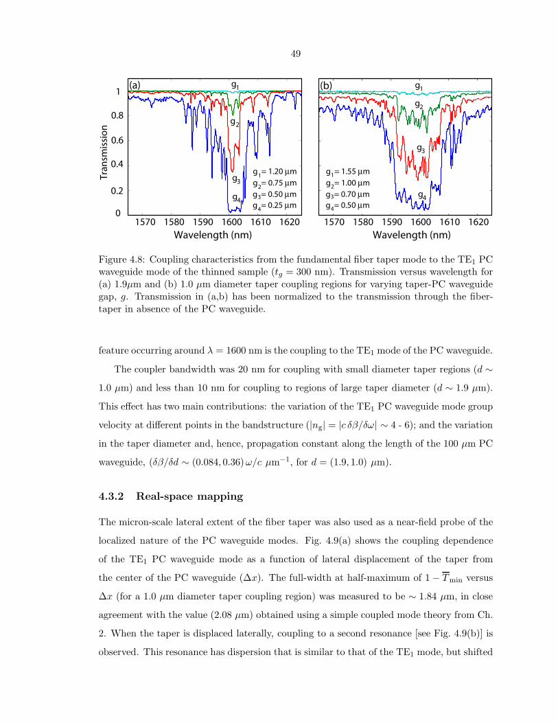
49
1570 1580 1590 1600 1610 16200
Tran
smis
sio
n
g1
g2
g4
g3
g1
g2
g3
g4
1570 1580 1590 1600 1610 1620
(a) (b)1
0.8
0.6
0.4
0.2
g = 1.55 μm1
g = 1.00 μm2
g = 0.70 μm3
g = 0.50 μm4
g = 1.20 μm1g = 0.75 μm2g = 0.50 μm3
g = 0.25 μm4
Wavelength (nm) Wavelength (nm)
Figure 4.8: Coupling characteristics from the fundamental fiber taper mode to the TE1 PCwaveguide mode of the thinned sample (tg = 300 nm). Transmission versus wavelength for(a) 1.9μm and (b) 1.0 μm diameter taper coupling regions for varying taper-PC waveguidegap, g. Transmission in (a,b) has been normalized to the transmission through the fiber-taper in absence of the PC waveguide.
feature occurring around λ = 1600 nm is the coupling to the TE1 mode of the PC waveguide.
The coupler bandwidth was 20 nm for coupling with small diameter taper regions (d ∼1.0 μm) and less than 10 nm for coupling to regions of large taper diameter (d ∼ 1.9 μm).
This effect has two main contributions: the variation of the TE1 PC waveguide mode group
velocity at different points in the bandstructure (|ng| = |c δβ/δω| ∼ 4 - 6); and the variation
in the taper diameter and, hence, propagation constant along the length of the 100 μm PC
waveguide, (δβ/δd ∼ (0.084, 0.36)ω/c μm−1, for d = (1.9, 1.0) μm).
4.3.2 Real-space mapping
The micron-scale lateral extent of the fiber taper was also used as a near-field probe of the
localized nature of the PC waveguide modes. Fig. 4.9(a) shows the coupling dependence
of the TE1 PC waveguide mode as a function of lateral displacement of the taper from
the center of the PC waveguide (Δx). The full-width at half-maximum of 1 − Tmin versus
Δx (for a 1.0 μm diameter taper coupling region) was measured to be ∼ 1.84 μm, in close
agreement with the value (2.08 μm) obtained using a simple coupled mode theory from Ch.
2. When the taper is displaced laterally, coupling to a second resonance [see Fig. 4.9(b)] is
observed. This resonance has dispersion that is similar to that of the TE1 mode, but shifted

50
Lateral Taper Position, Δx (μm)0 42-2-4
1
0
1 - T
even modeodd mode
odd mode
Δx=1μm
1570 1580 1590 1600 1610 1620Wavelength (nm)
(a) (b)
1
0
T
even mode
Figure 4.9: Coupling characteristics from the fundamental fiber taper mode to the TE1 PCwaveguide mode of the thinned sample (tg = 300 nm). (a) 1 − Tmin versus lateral position(Δx) of the 1.0 μm diameter fiber taper relative to the center of the PC waveguide (g = 400nm). (b) Transmission versus wavelength for Δx ∼ 1 μm. Transmission in (a-b) has beennormalized to the transmission through the fiber-taper in absence of the PC waveguide.
∼ 30 nm lower in wavelength, and corresponds to coupling to the odd (about x) counterpart
to the TE1 mode. The coupling is a result of the broken mirror symmetry about x induced
by the taper when |Δx| > 0, and is a further demonstration of the local nature of the taper
probe.
4.4 Efficient coupling into PC microcavities
Having demonstrated above that nearly ideal coupling from a fiber taper into a well char-
acterized PC waveguide mode is possible, the next step was to integrate the fiber-coupled
PC waveguide with a PC microcavity, and efficiently fiber couple light into and out of the
wavelength scale resonator. Following the design presented in Ch. 2, and using the same
fabrication techniques described Sec. 4.1.3 to realize the PC waveguide devices discussed
above, integrated PC cavity-PC waveguide devices were fabricated in a tg = 340nm thick
layer of Si. A typical device is shown in Fig. 4.10, which also shows regions in which un-
patterned silicon was removed to allow taper probing of the device. In addition to isolating
the PC devices on a mesa of height ∼ 10 μm, a trench extending diagonally from the cavity

51
PC cavity center
PCWGtrench
isolationregion
top Si layer(340 nm)
Λx
Λz
Λ
2 μm10 μm
Figure 4.10: SEM image of an integrated PC waveguide-PC cavity sample. The PC cavityand PC waveguide have lattice constants Λ ∼ 430 nm, Λx ∼ 430 nm, and Λz ∼ 550 nm. Thesurrounding silicon material has been removed to form a diagonal trench and an isolatedmesa structure to enable fiber taper probing.
was defined. This allowed the cavity to be probed directly by the fiber taper, independently
from the waveguide, as in Ref. [11]. However, as described below, much more efficient cou-
pling to the PC cavity was also performed by aligning the fiber taper along the axis of the
PC waveguide and coupling through the PC waveguide into the PC cavity, as described
theoretically in Ch. 2
Direct taper-cavity probing
With the taper aligned with the etched trench, the spectral and spatial properties of the
PC cavity modes were probed directly [Fig. 4.11(a), taper position (ii)], as in Ref. [11]. The
trench prevented the fiber taper from interacting with the unpatterned silicon, and light
was coupled directly from the fiber taper into the high-Q PC cavity modes. Although this

52
Δx
Fiber taper orientations:
PC cavity
PCWG
Trench
Undercut perimeter
0-1 1 2-20
1
0.2
0.4
0.6
0.8
Δx (μm)
(a) (b)
ΔT /
Max
(ΔT)
(i) (ii)
Figure 4.11: (a) Illustration of the device and fiber taper orientation for (i) efficient PCwaveguide mediated taper probing of the cavity, and (ii) direct taper probing of the cavity.(b) Normalized depth of the transmission resonance (ΔT ) at λo ∼ 1589.7, as a functionof lateral taper displacement relative to the center of the PC cavity, during direct taperprobing (taper in orientation (ii)).
coupling is inefficient (ΔT =1-10%, I � 1), it allowed the frequency of the A02 cavity mode
to be independently determined.
In the device studied here, when the taper was aligned with the trench and positioned
∼ 500 nm above the cavity, a sharp dip in T was observed at a wavelength of λo ∼ 1589.7
nm. It was confirmed that this was due to coupling to a localized cavity mode by studying
the depth of the resonance as the taper was displaced laterally (|Δx| > 0) relative to
the center of the PC-cavity. The measured normalized resonance depth as a function of
taper displacement is shown in Fig. 4.11(b), and has a halfwidth of 480 nm, consistent
with previous studies of the localized A02 cavity mode [11]. To further aid with the initial
differentiation between resonant features in the transmission that are due to cavity modes
from those that are due to delocalized Fabry-Perot reflections within the PC lattice, it
is useful to monitor the reflected signal in the fiber taper during this step. Because of
their localized nature, PC cavity modes couple into the backward and forward propagating
fiber taper modes with equal efficiency, usually resulting in distinct features in the reflected
signal.

53
PC waveguide mediated taper-cavity probing
The fiber taper was then aligned above and parallel to the PC waveguide (Fig. 4.11(a), taper
position (i)). At taper-PC waveguide phase-matching wavelengths, T decreases resonantly
as power is coupled from the taper into the PC waveguide; coupling to the TE1 PC waveg-
uide mode was verified by studying the dispersive and spatial properties of the coupling, as
in Sec. 4.3. The fiber taper-PC waveguide coupling bandwidth was adjusted to overlap with
the wavelength of the A02 cavity mode using two mechanisms. Coarse tuning was obtained
by adjusting, from sample to sample, the nominal hole size and longitudinal lattice constant
(Λz) of the PC waveguide. Fine tuning of the coupler’s center wavelength over a 100 nm
wavelength range was obtained by adjusting the position, and, hence, the diameter of the
fiber taper region coupled to the PC waveguide [47]. Different degrees of cavity loading
were also studied by adjusting the number of periods (9-11) of air holes between the center
of the PC cavity and the end of the PC waveguide. In the device studied below (shown in
Fig. 4.10) the PC cavity was fabricated with nine periods on the side adjacent to the PC
waveguide and 18 periods on the side opposite the PC waveguide .
Figure 4.12(a) shows the normalized reflected fiber signal, R, for a taper diameter d ∼ 1
μm, which aligns the taper-PC waveguide coupler bandwidth with the A02 PC cavity mode
wavelength. This signal is normalized to the taper transmission in absence of the PC
waveguide, and since light passes through the taper-PC waveguide coupler twice, the signal
is given by R = η2wgRo, where ηwg is the taper-PC waveguide coupling efficiency. Note that
both Ro and ηwg are frequency dependent. In Fig. 4.12(a), the peak in R around λ ∼ 1590
nm corresponds to the phase-matched point of the fiber taper and the TE1 PC waveguide
mode. From the peak value of Rmax = 0.53, a maximum taper-PC waveguide coupling
efficiency of ηwg ∼ 73% was estimated, where the off-resonant Ro is taken to be unity.
This value is lower than the 97% obtained in Sec. 4.2 due to coupling to additional higher-
order (normal to the Si slab) PC waveguide modes that interfere with the coupling to the
fundamental TE1 PC waveguide mode for strong taper-PC waveguide coupling. This can be
avoided in future devices by increasing the nominal PC waveguide hole size relative to that
in the PC-cavity or reducing the Si slab thickness, effectively freezing out the higher-order
PC waveguide modes [47].
The sharp dip in reflection at λ ∼ 1589.7 nm, shown in detail in Fig. 4.12(b), corresponds

54
1584 15940
0.2
0.4
0
0.5
1
0.4 0.6 0.8 1.0 1.2 1.4
ΔR Rmax
Taper height g (μm)
Wavelength (nm)
0.6
1589.5 1589.8Wavelength (nm)
(a)
(b)
Δλ = 41.5 pm
Refle
ctio
n, R
0.2
0.4
0.6
Refle
ctio
n, R
1586 1588 1590 1592
(c)
Figure 4.12: (a) Measured reflected taper signal as a function of input wavelength (taperdiameter d ∼ 1 μm, taper height g = 0.80 μm). The sharp dip at λ ∼ 1589.7 nm, highlightedin panel (b), corresponds to coupling to the A0
2 cavity mode. (c) Maximum reflected signal(slightly detuned from the A0
2 resonance line), and resonance reflection contrast as a functionof taper height. The dashed line at ΔR = 0.6 shows the PC waveguide-cavity drop efficiency,which is independent of the fiber taper position for g ≥ 0.8 μm.
to resonant excitation of the A02 PC cavity mode, as confirmed by the direct fiber probing of
the cavity described above. The other broad features in R correspond to weak Fabry-Perot
effects of the PC waveguide, and weak interference between the TE1 mode and higher order
PC waveguide modes. The reflected fiber taper signal as a function of taper-PC waveguide
gap height, g, is shown in Fig. 4.12(c). For g ≥ 0.8 μm, Rmax increases with decreasing
g as the coupling from the fiber taper to the TE1 PC waveguide mode becomes stronger.
The resonance contrast, ΔR = 1−Ro(ωo) = (Rmax−R(ωo))/Rmax, remains constant, since
the PC waveguide-cavity interaction is independent of the fiber taper to PC waveguide
coupling. For smaller taper-PC waveguide gap heights, g < 0.8 μm, fiber taper coupling
into higher order PC waveguide modes and radiation modes becomes appreciable, and Rmax
decreases for decreased taper height. The corresponding increase in ΔR seen in Fig. 4.12(c)

55
is a result of interference between the TE1 mode and higher-order PC waveguide modes
that are excited and collected by the taper, and is not a manifestation of improved coupling
between the TE1 PC waveguide mode and the A02 PC cavity mode. Direct coupling between
the taper and the cavity is negligible here.
From a Lorentzian fit to the A02 cavity resonance dip in Ro(ω), the normalized on-
resonance reflected power is estimated to be Ro(ωo) = 0.40, corresponding to an undercou-
pled K = 0.225. The loaded quality factor as measured by the reflected signal linewidth is
QT = 3.8×10⁴. Substituting these values into Eq. (3.4) gives the cavity mode quality factor
due to parasitic loading and intrinsic losses, Qi+P = 4.7 × 10⁴. Previous measurements of
similar PC cavity devices without an external PC waveguide load yielded intrinsic quality
factors of 4×10⁴ [11], strongly indicating that the parasitic loading of the PC cavity by the
PC waveguide is minimal, and I ∼ 1 for this PC cavity-waveguide system. The high ideality
of this coupling scheme should be contrasted with previous direct taper measurements of
the PC cavities [11], whose coupling was limited to a maximum value, K = 0.018, with an
ideality of I ∼ 0.035 (corresponding to a resonance depth of 7%, QT = 2.2 × 10⁴).
The efficiency of power transfer from the fiber taper into the PC cavity is given by
ηin = ηwgΔR ≈ 44%. This corresponds to the total percentage of photons input to the
fiber taper that are dropped by the PC cavity. Based upon these measurements, in the
case of an internal cavity source, such as an atom or a quantum dot, the efficiency of light
collection into the fiber taper for this PC cavity system would be ηout = ηwgη0 ≈ 13%
(η0 ≈ 18%). As the tapers themselves are of comparably very low loss, with typical losses
associated with the tapering process less than 10%, these values accurately estimate the
overall optical fiber coupling efficiency. Finally, note that previous measurements of near-
ideal coupling between the fiber taper and PC waveguide indicate that by adjusting the PC
waveguide as described above to improve ηwg, ηin, and ηout can be increased to 58% and
18%, respectively. More substantially, adjustments in the coupling parameter, K, towards
over-coupling by decreasing the number of air-hole periods between the PC cavity and the
PC waveguide can result in significant increases in ηin and ηout, with minimal penalty in
loaded Q-factor for I ∼ 1.

56
4.5 Conclusion
The evanescent fiber taper to PC waveguide coupling technique demonstrated is this chapter
provides unprecedentedly high coupling efficiency, as well as a means to study both the
dispersive and spatial properties of bound photonic crystal waveguide modes, and an optical
channel to source high-Q PC microcavities. These results confirm the theoretical predictions
of the previous chapters, and reinforce the utility of fiber tapers as wafer-scale probes for
photonic crystal devices. In the next chapter, we will leverage this technique to study the
nonlinear optical properties the PC microcavity.
57
Chapter 5
Nonlinear optics in silicon photoniccrystal cavities
Owing to the ultra-small mode volume and long resonant photon lifetimes of PC cavities,
the resulting stored electromagnetic energy density can be extremely large even for modest
input powers (< mW), resulting in highly nonlinear behavior of the resonant cavity system.
Having demonstrated in Ch. 4 a technique for efficiently coupling light into a small mode
volume, high-Q, silicon PC cavity, we now have the tools necessary to study nonlinear
optical properties intrinsic to these devices.
In this chapter, we present results demonstrating optical bistability in a silicon PC cavity
for 100 μW dropped CW cavity power. By comparing a model of the relevant nonlinear
optical process within these devices with the observed results, we are able to understand
which nonlinear effects play the largest role, and extract parameters describing physical
properties of Si within nanophotonic devices. In particular, we predict sub-nanosecond free
carrier lifetimes in the cavity, which, due to the small mode volume and large effective
surface area of these devices, are significantly shorter than are found in bulk Si.
Since the publication of these results in Ref. [25], a number of groups have observed sim-
ilar nonlinear effects in PC microcavities, and have taken advantage of them to implement
low-power high-speed optical switches [26, 90, 91, 92]. In addition, from a technological
perspective, the importance of nonlinear absorption and free-carriers effects in nanopho-
tonic devices fabricated from silicon has continued to grow, as recent progress in optical
modulators [93] and wavelength converters [94, 95] has relied upon engineering devices while
taking these effects into careful consideration.
We begin in Sec. 5.1 by generalizing the linear waveguide-cavity coupling theory of Sec.
3.1 to include nonlinear processes that depend upon the magnitude of the internally stored

58
cavity energy. Higher power measurements in which nonlinear effects become apparent are
studied in Sec. 5.2, and the model presented in Sec. 5.1 is used to estimate the scale of the
various nonlinear effects within the silicon PC cavity.
5.1 Modeling nonlinear absorption and dispersion in a mi-
crocavity
In order to account for nonlinear effects one may modify the (linear) analysis of Sec. 3.1
by allowing the various cavity and coupling parameters to depend upon the stored cavity
energy, a reasonably easy quantity to estimate from experimental measurements. In this
section, relevant nonlinear processes are explicitly incorporated into the description of the
cavity response through use of carefully defined effective modal volumes and confinement
factors appropriate to nonlinear processes in high-index contrast photonic crystal structures.
We begin with a description of nonlinear absorption, which tends to drive the steady-state
nonlinear response of the PC cavities studied here.
5.1.1 Nonlinear absorption
Nonlinear absorption adds power dependent loss to the photonic crystal cavity, degrading
the quality factor as the internal cavity energy is increased, which in turn modifies the
coupling efficiency from the PC waveguide loading channel. This effect is incorporated into
the formalism presented in Sec. 3.1 by writing the intrinsic cavity loss rate, γi, explicitly in
terms of its various linear and nonlinear components:
γi(U) = γrad + γlin + γTPA(U) + γFCA(U). (5.1)
At low power, the “cold cavity” loss rate is given by γrad and γlin, which represent loss due
to radiation and linear material absorption, respectively. Power dependent nonlinear loss is
given here by γTPA and γFCA, which represent two-photon and free-carrier absorption, re-
spectively; other nonlinear absorption processes can be included analogously. The coupling
parameter K and the quality factor Qi+P depend on γi, requiring the solution of a system
of self-consistent equations for U in order to determine the on-resonance cavity response for

59
a given PC waveguide input power Pi:
U =4K(U)
(1 +K(U))2Qi+P (U)
ωoPi, (5.2)
K(U) =γe
o
γi(U) +∑
j>0 γej
, (5.3)
ωo
Qi+P (U)= γi(U) +
∑j>0
γej . (5.4)
Before Eqs. (5.2-5.4) can be solved, explicit expressions for the energy-dependent contribu-
tions to γi are required. Beginning with relations for nonlinear absorption in bulk media,
and taking into account the complicated geometry of the PC cavity, we now derive expres-
sions for γTPA and γFCA. These expressions can be written in terms of the internal cavity
energy, known material parameters, and modal parameters that account for the mode shape
and localization of the PC cavity field.
Two-photon absorption
The 1500 nm operating band of the devices studied in this work lies in the bandgap of the
host silicon material. For the doping densities of the p-type silicon membrane used to form
the PC cavity (ρ ∼ 1 − 3 Ω · cm, NA < 1016 cm−3), free-carrier absorption due to ionized
dopants is small (αfc ∼ 10−2 cm−1). Two-photon absorption, however, is significant[60, 96,
97, 98, 99], especially in the highly localized PC cavities. For a given field distribution, the
(time-averaged) two-photon absorption loss rate at position r can be written as
γTPA(r) = β′(r)12εon
2(r)E2(r), (5.5)
where E(r) is the amplitude of the complex electric field pattern, E(r), of the resonant
mode of the cavity; εo is the permittivity of free space; and n(r) is the local (unperturbed)
refractive index. The real, physical electric field of the resonant cavity mode can be written
in terms of the complex mode pattern as E(r, t) = (E(r)e−iωot + E∗(r)e+iωot)/2. The
material parameter, β′, describes the strength of the two-photon absorption process, and
can be related to the usual two-photon absorption coefficient, β, that relates intensity to
loss per unit length, by β′ = (c/ng)2β, where c is the speed of light in vacuum and ng is the
group velocity index associated with the measurement of β. Typically, for bulk material

60
measurements where waveguiding is minimal and material dispersion is small, ng can be
taken to be equal to n.
In high-index-contrast photonic crystals, E, n, and β′ depend strongly on the spatial
coordinate r. Equation (5.5) describes the local two-photon absorption rate; the effective
modal two-photon absorption rate that characterizes the absorption of the entire cavity
mode is given by a weighted average of the local absorption rate [100, 101],
γTPA =∫γTPA(r)n2(r)E2(r)dr∫
n2(r)E2(r)dr= β′
U
VTPA, (5.6)
where β′ and VTPA are defined as
β′ =∫β′(r)n4(r)E4(r)dr∫n4(r)E4(r)dr
(5.7)
VTPA =
(∫n2(r)E2(r)dr
)2∫n4(r)E4(r)dr
. (5.8)
In a photonic crystal formed by air holes in silicon, β′(r) = β′Si inside the silicon, and
β′(r) = 0 in the air, so that Eq. (5.6) can be written as,
γTPA = ΓTPAβ′Si
U
VTPA(5.9)
ΓTPA =
∫Si n
4(r)E4(r)dr∫n4(r)E4(r)dr
, (5.10)
for which∫Si only integrates over the silicon region of the PC cavity.
Free-carrier absorption
Although, as mentioned above, the (linear) free-carrier absorption due to the ionized dopants
of the silicon layer used for the PC cavities in this work is negligible on the scale of other
losses, two-photon absorption gives rise to a steady-state population of electron and hole
free-carriers far above this equilibrium value. Two-photon absorption induced free-carrier
absorption thus plays a significant role in the silicon PC cavity nonlinear response. At
position r in the cavity, assuming a simple Drude model, the optical loss rate due to free-
carrier absorption is
γFCA = σ′(r)N(r), (5.11)

61
where σ′ is related to the material dependent free-carrier cross-section, σ, by σ′ = σ(c/ng),
and N(r) is the free-carrier density. In silicon, it has been demonstrated experimentally
[102] that this model correctly describes absorption by both electrons and holes, albeit with
unique values of σ′e,h for each carrier type. Here we let N represent the number of electron-
hole pairs and take σ′ = σ′e + σ′h. We neglect the small (< 1 × 1016 cm−3) background
free-carrier hole density due to the ionized acceptors of the p-type Si layer used in this
work.
In general, the derivation of the free-carrier density for a given two-photon absorbed
power distribution requires a microscopic theory that takes into account carrier diffusion,
carrier-carrier scattering effects (Auger recombination, for instance), and, in the highly
porous PC cavities, local surface recombination effects. In lieu of such an analysis, we ap-
proximate the free-carrier density distribution by considering the local two-photon absorbed
power,
N(r) =τpTPA(r)
2�ωo, (5.12)
where τ is a free-carrier lifetime, and pTPA(r) is the local absorbed power density due to
two-photon absorption,
pTPA(r) =12εon
2(r)E2(r)γTPA(r). (5.13)
Equation (5.12) neglects non-local effects due to spatial carrier diffusion by assuming that
N(r) depends only on the power absorbed at position r; however, it does correlate regions of
strong two-photon absorption with high free-carrier density. Also, since τ generally depends
on N and on the proximity to surfaces, τ will have a spatial dependence within the cavity.
We neglect this effect here, and let τ represent an effective free-carrier lifetime for all the
carriers in the cavity region1. Combining Eqs. (5.11), (5.12), and (5.13), an effective modal
free-carrier absorption rate can be written as
γFCA =τ
2�ωo
∫ (σ′(r)1
2εon2(r)E2(r)γTPA(r)
)n2(r)E2(r)dr∫
n2(r)E2(r)dr. (5.14)
Substituting Eq. (5.5) for γTPA(r), the modal loss rate due to free-carrier absorption in the
1In using the approximate theory above, in which regions of high two-photon absorbed power are cor-related with high steady-state carrier density, we better approximate the cavity “volume” of interest, andconsequently the effective free-carrier lifetime better represents the average time a free-carrier stays in theregion of the PC cavity mode.

62
porous silicon photonic crystals considered here can be written as
γFCA = ΓFCA
(τσ′Siβ
′Si
2�ωo
U2
V 2FCA
), (5.15)
with effective confinement factor and mode volume defined as
ΓFCA =
∫Si n
6(r)E6(r)dr∫n6(r)E6(r)dr
(5.16)
V 2FCA =
(∫n2(r)E2(r)dr
)3∫n6(r)E6(r)dr
. (5.17)
Equations (5.15) and (5.9) represent the total loss rate of photons from the cavity due
to free-carrier and two-photon absorption, respectively. These expressions depend only
on material parameters; modal confinement factors, ΓTPA,FCA; effective mode volumes,
VTPA,FCA; and the internal cavity energy, U . The modal parameters take into account the
non-trivial geometry and field distribution of the cavity mode, and can be determined for
a given mode from FDTD simulations. Including expressions (5.9) and (5.15) in γi, Eqs.
(5.2-5.4) can be solved iteratively for Qi+P and K, which characterize the on-resonance
nonlinear response of the cavity for a given input power.
5.1.2 Nonlinear and thermal dispersion
In addition to modifying the cavity quality factor, large cavity energy densities also modify
the refractive index of the cavity, resulting in a power dependent resonance frequency. Here
we consider the role of the Kerr effect, free-carrier dispersion, and heating due to linear
and nonlinear absorption, on the dispersive response of the PC cavity. The refractive index
shift induced through the processes considered here is a function of both space and internal
cavity energy. The corresponding renormalization of the resonant cavity frequency can be
approximated using first order perturbation theory as
Δωo(U)ωo
= −Δn(U), (5.18)

63
where the normalized modal index shift, Δn(U), is given by an average of the (normalized)
local refractive index shift, Δn(r)/n(r):
Δn(U) =
∫ (Δn(r)n(r)
)n2(r)E2(r)dr∫
n2(r)E2(r)dr. (5.19)
This energy dependent frequency shift, together with the energy dependent loss described
in Sec. 5.1.1, modifies the Lorentzian frequency dependence of the cavity response:
Ro(ω) = 1 − 4K(U)(1 +K(U))2
(δω/2)2
(ω − ωo − Δωo(U))2 + (δω(U)/2)2. (5.20)
For a given input power Pi and frequency ω, U is given by
U =Pd
γi+P= (1 −Ro(ω))
Qi+P (U)ωo
Pi, (5.21)
where Pd = (1−Ro(ω))Pi is the frequency dependent dropped power in the resonant cavity.
For input powers sufficient to shift Δωo >√
3δω/2, the frequency response described by
Eq. (5.20) is bistable, and can be exploited for applications including temperature locking
and optical switching [103, 24, 104]. In order to solve Eq. (5.20) for the cavity response, it
is necessary to derive expressions for each of the constituents of Δn as a function of U . We
begin with the Kerr effect.
Kerr effect
The time-averaged local index shift induced by the Kerr effect is
ΔnKerr(r) = n′2(r)12εon
2(r)E2(r), (5.22)
where n′2(r) is a material parameter, and is related to the usual n2 coefficient relating
intensity to refractive index shift [105] by n′2 = (c/ng)n2. In a silicon PC cavity, neglecting
the tensor nature of the third order susceptibility, the normalized modal index change due
to the Kerr effect can be written as
ΔnKerr(U) =ΓKerr
nSi
(n′2,Si
U
VKerr
), (5.23)

64
with n′2,Si and nSi being the Kerr coefficient and linear refractive index of Si, respectively.
A similar, more general expression, is given in Ref. [106]. As both the Kerr effect and two-
photon absorption (TPA) share the same dependence on field strength, the confinement
factor and effective mode volume associated with the Kerr effect are equal to those of TPA:
ΓKerr = ΓTPA (5.24)
VKerr = VTPA. (5.25)
Free-carrier dispersion
Dispersion due to free-carrier electron-hole pairs is given by2
ΔnFCD(r) = −ζ(r)N(r), (5.27)
where ζ(r) is a material parameter with units of volume. Following the derivation of γFCA,
the normalized modal index change is
ΔnFCD(U) = −ΓFCD
nSi
(τζSiβ
′Si
2�ωo
U2
V 2FCD
), (5.28)
with
ΓFCD = ΓFCA (5.29)
VFCD = VFCA. (5.30)
Thermal dispersion
It is also necessary to consider the effect of thermal heating due to optical absorption on
the refractive index of the PC cavity. The normalized modal index shift is given by
Δnth =
∫ (1
n(r)dndT (r)ΔT (r)
)n2(r)E2(r)dr∫
n2(r)E2(r)dr. (5.31)
2Experimental results [102] indicate that this Drude model must be modified slightly to accurately de-scribe the contribution from hole free-carriers in silicon, which scales with N0.8
h :
ΔnFCD,Si = − �ζe,SiNe + (ζh,SiNh)0.8
�. (5.26)
For simplicity, we ignore this in the following analysis, and note that the modification is straightforward,and is included in later numerical results.

65
Here ΔT (r) is the local temperature change due to the absorbed optical power density
within the cavity, and dn/dT is a material dependent thermo-optical coefficient. Neglect-
ing differences in the spatial distributions of the contributions to ΔT (r) from the various
absorption processes, and assuming that ΔT (r) scales linearly with absorbed power density
for a fixed spatial heating distribution, the modal thermal shift can be written as
Δnth(U) =Γth
nSi
(dnSi
dT
dT
dPabsPabs(U)
)(5.32)
where,
Pabs(U) =(γlin + γTPA(U) + γFCA(U2)
)U. (5.33)
Γth =∫Si n
2E2dr/∫n2E2dr is a confinement factor that accounts for the fact that only
the semiconductor experiences an appreciable index shift, and dT/dPabs is the thermal
resistance of the PC cavity, which relates the mean modal temperature change to the total
absorbed power. In what follows, we lump these two factors together, yielding an effective
thermal resistance of the PC cavity.
From Eqs. (5.23), (5.28), and (5.32), the total modal index change and corresponding
resonance frequency shift can be determined as a function of cavity energy. The nonlinear
lineshape described by Eq. (5.20) can then be calculated iteratively as a function of input
power when combined with the power dependent loss model of sub-section 5.1.1. This is
used below in Sec. 5.2 to estimate the scale of the different nonlinear processes in silicon
PC microcavities.
As a final comment, we note that the above analysis has assumed steady-state optical,
carrier, and thermal distributions, whereas the transient response of such structures is of sig-
nificant practical interest for applications such as high speed switching. Although the Kerr
nonlinearity, two-photon absorption, free-carrier absorption, and free-carrier dispersion all
depend on the electronic structure of the semiconductor material, the sub-micron geometry
typical of photonic crystals can also play an important role. For example, the surfaces
introduced by the slab and air hole geometry of planar PC cavities can significantly modify
the free-carrier lifetime, τ , compared to that in bulk material [103, 107, 108]. Similarly,
the thermal response time scales inversely with the spatial scale of the optically absorbing

66
region, and depends upon the geometry and the material dependent thermal properties of
a given structure [105]. Although not the focus of the work presented here, an inkling of
these effects is seen in the sub-nanosecond estimated effective free-carrier lifetime in the
silicon PC cavity studied below.
5.2 Nonlinear measurements
The nonlinear response of the PC cavity was studied by measuring the dependence of
the reflected signal lineshape on the power input to the PC waveguide. Figure 5.1 shows
wavelength scans of the cavity response, Ro, for varying power, Pt, input to the fiber taper.
Each scan was obtained by dividing the normalized reflected signal, R, by the slowly varying
taper-PC waveguide coupler lineshape, η2wg(ω). In all of the measurements, the fiber taper
was aligned near the optimal taper-PC waveguide coupling position, and the wavelength of
the laser source was scanned in the direction of increasing λ. Pt was determined by taking
taper insertion loss into account, and measuring the taper input power with a calibrated
power meter.
Increasing the power in the fiber taper, and consequently the PC waveguide, results in
three readily observable changes in Ro: (i) a decrease in the resonance contrast, ΔRo; (ii)
a shift Δωo in the resonance frequency ωo; and (iii) the broadening and asymmetric distor-
tion of the resonance lineshape, eventually leading to a “snap” in the reflection response
characteristic of bistability [109]. Here we use the theory presented in Sec. 5.1 to show that
these features are due to nonlinear absorption and dispersion in the PC cavity.
Figure 5.2(a) shows Pd, the on-resonance power dropped into the PC cavity, as a function
of Pi, the power incident on the cavity from the PC waveguide. Pd is measured from
Pd = ΔRo(Pi)Pi, and Pi is related to the taper input power by Pi = ηwg(ωo)Pt. For
small Pi, Pd increases with a constant slope equal to the “cold cavity” value of ΔRo = 0.60
measured in Sec. 4.4. For larger Pi, Pd becomes sub-linear versus Pi, as loss due to nonlinear
absorption becomes appreciable compared to the other loss channels of the PC cavity. In
the context of the analysis of Sec. 5.1, γi increases with increasing Pd, degrading K, and
decreasing ΔRo (for K < 1). From the “cold cavity” η0 and QT measured in the previous

67
Wavelength (nm)
1589.5 1589.6 1589.7 1589.8 1589.9 1590.0 1590.1 1590.2
Ro
0.4
0.9
1.0
0.8
0.5
0.6
0.7
1.2E-1 mW
2.0E-1 mW
4.5E-1 mW6.6E-1 mW
8.8E-1 mW
8.1E-4 mW
2.1E-2 mW
Figure 5.1: (a) Measured cavity response as a function of input wavelength, for varying PCwaveguide power (taper diameter d ∼ 1 μm, taper height g = 0.80 μm).
section, the power dependentQi+P (Pi) can be extracted from ΔRo(Pi) through the relation:
Qi+P (Pi) = K(ΔRo(Pi))QT (Pi = 0)η0(Pi = 0)
. (5.34)
Equation (5.34) is useful for powers where nonlinear effects distort the Lorentzian lineshape,
and λo/δλ is not an accurate measure of QT (Pi). Using Eqs. (5.34) and (3.7), the internal
cavity energy, U , can be calculated from Pi and ΔRo.
Figure 5.2(b) shows a plot of the measured Δλo, the resonance wavelength shift, as a
function of U 3. This plot has several noteworthy properties: First, the wavelength shift
is nonlinear in U , indicating that nonlinear processes such as free-carrier dispersion and
heating through nonlinear absorption must be taking effect. Also, for small U , the resonance
wavelength is seen to blue shift. In the 1550 nm wavelength band of operation, both dnSi/dT
and n2,Si are > 0, while d(ΔnFCD)/dU < 0, indicating that free-carrier dispersion is the
3Note that the sharp transition edge associated with optical bistability occurs at the cavity resonancewavelength when scanning from blue to red, thus an accurate measure of Δλo can be made.

68
Pi (mW)
P d (
mW
)
0.20 0.60.4 0.80
0.4
0.3
0.2
0.1
0.5
0
0.4
0.2
U (fJ )0 5 10
Δλo
(n
m)
(a)
210 U (fJ )
5
10
0
15
20
-5
Δλo
(p
m)
(b)
Figure 5.2: (a) Power dropped (Pd) into the cavity as a function of power in the PCwaveguide (Pi). The dashed line shows the expected result in absence of nonlinear cavityloss. (b) Resonance wavelength shift as a function of internal cavity energy. Solid blue linesin both Figs. show simulated results.
dominant dispersive process at low input powers. For U > 0.34 fJ (Pd > 10 μW), the
resonance wavelength begins to red shift, indicating that thermal or Kerr effects dominate
for large internal cavity energy. Also, note that for a stored cavity energy as low as U ∼ 3
fJ (Pd ∼ 100 μW) the cavity response is bistable with Δλo = 35 pm ∼ √3δλ/2.
In order to estimate the contributions of the various nonlinear processes to the effects
discussed above, the absorptive, Pd(Pi), and dispersive, Δλ(Pi), data were fit using the
model presented in Sec. 5.1. Specifically, Eqs. (5.2-5.4) were solved for Pd and U as a
function of Pi, and Eq. (5.18) was used to calculate Δλo. The free parameters in this model
were taken as: (i) the effective free-carrier lifetime, τ ; (ii) the effective thermal resistance
of the PC cavity, ΓthdT/dPabs; and (iii) the fraction of the “cold cavity” loss that is due
to linear absorption (as opposed to radiation), ηlin = γlin/(γlin + γrad). The material and
modal constants used are listed in Table 5.1.

69
Table 5.1: Nonlinear optical coefficients for the Si
photonic crystal microcavity.
Parameter Value Units Source
VTPA 4.90 (λo/nSi)3 FDTDb
VFCA 3.56 (λo/nSi)3 FDTDb
ΓTPA 0.982 - FDTDb
ΓFCA 0.997 - FDTDb
nSi 3.45 - [110, 102]
σSi 14.5 × 10⁻²² m2 [110, 102]
ζeSi 8.8 × 10⁻²⁸ m3 [110, 102]
ζhSi 4.6 × 10⁻²⁸ m3 [110, 102]
n2,Si 4.4 × 10⁻¹⁸ m2 · W−1 [96]
βSi 8.4 × 10⁻¹² m · W−1 [96]a
dnSi/dT 1.86 × 10⁻⁴ K−1 [111]
a Average of the two quoted values for Si〈110〉and Si〈111〉.
b Calculated from FDTD generated fields of the
A02 cavity mode of the graded square lattice
cavity studied here.
As has been observed in studies of silicon optical waveguides [97], we find that a strong
dependence of τ on carrier density is required for our model, to accurately reproduce both
the dispersive and absorptive data represented in Figs. 5.3(a) and (b). In order to account
for a carrier density dependent lifetime in our model the following procedure was used:
With ΓthdT/dPabs and ηlin held fixed, τ(Pi) was determined for each input power from a
least squares fit to Δλo(Pi) and Pd(Pi). Since there are two data points for each input
power, one dispersive and one absorptive, the optimum τ(Pi) has a non-zero residual error.

70
Pd (mW )0 0.2 0.4
Pd (mW )0 0.2 0.4
1 /
Q
0
1
1.4x 10⁻⁵
1 / QTPA
1 / QFCA
1 / Qlin
1 / Qrad
0
0.2
0.4
Δλo
(n
m)
-0.2
Thermal - TPAThermal - FCA
FCDKerrTotal
Thermal - lin
(a) (b)
-0.4
Figure 5.3: (a) Simulated effective quality factors for the different PC cavity loss channels asa function of power dropped into the cavity. (b) Contributions from the modeled dispersiveprocesses to the PC cavity resonance wavelength shift as a function of power droppedinto the cavity. (Simulation parameters: ηlin ∼ 0.40, ΓthdT/dPabs = 27 K/mW, τ−1 ∼0.0067 + (1.4 × 10⁻⁷)N0.94 where N has units of cm−3 and τ has units of ns.)
This procedure was repeated for a range of values for ΓthdT/dPabs and ηlin. For a fixed
value of ηlin, the fits were robust in ΓthdT/dPabs with the sum of the least square residual
of τ(Pi) clearly minimized for an optimal value of ΓthdT/dPabs. This procedure, however,
was only found to constrain ηlin > 0.15. Within this range of ηlin the quality of the fits
does not change significantly, with the optimal functional form of τ changing slightly and
the optimal value of ΓthdT/dPabs varying between ∼ 15 − 35 K/mW. Based on estimates
of ηlin from studies of loss in silicon microdisk resonators fabricated using the same SOI
wafers and the same processing techniques [44], and by comparing the etched surface area
seen by the PC cavity mode to that seen by a microdisk mode, we chose to use ηlin ∼ 0.40
for the PC cavity. With this value of ηlin the optimal value of the effective cavity thermal
resistance, ΓthdT/dPabs, was found to be 27 K/mW, of the same order of magnitude as the
result calculated in Ref. [112] for a similar membrane structure. Finally, the point-by-point
least-squared optimum values of τ(Pi) were then fit as a function of the effective free-carrier
density N , using a curve of the form τ−1 = A + BNα . Using this τ(N), smooth fits to
measured Pd(Pi) and Δλ(Pi) were obtained, shown as solid blue lines in Fig. 5.2.
Fig. 5.3 shows the various components of the total cavity loss rate, and resonance shift,

71
-10
-7.5
-8
-9
0 8642Free-carrier density, N (cm-3)
x 1016
Log
10(τ
(s))
-8.5
-9.5
10 12
Figure 5.4: Dependence of free-carrier lifetime on free-carrier density (red dots) as foundby fitting Δλo(Pi) and Pd(Pi) with the constant material and modal parameter values ofTable 5.1, and for effective PC cavity thermal resistance of ΓthdT/dPabs = 27 K/mW andlinear absorption fraction ηlin = 0.40. The solid blue line corresponds to a smooth curvefit to the point-by-point least-squared fit data given by τ−1 ∼ 0.0067 + (1.4 × 10⁻⁷)N0.94,where N is in units of cm−3 and τ is in ns.
for the parameters used in the fits to the measured data. It can be seen that although TPA
does not dominate the PC cavity response, the free-carriers it generates and the resulting
free carrier dispersion and absorption drive the nonlinear behavior of the silicon PC cavity
at low and high input powers, respectively. The fit effective free-carrier lifetime, shown in
Fig. 5.4, shows similar characteristics to that obtained by Liang et al. [97], demonstrating
a significant fall-off in τ for large N , but with a smaller saturated lifetime. Both the
pronounced decay in τ and the low ∼ 0.5 ns value of the high-carrier density free-carrier
lifetime are significantly different from that found in bulk Si, and are most likely related to
carrier diffusion and surface effects owing to the extremely large surface-to-volume ratio of
the PC cavity, the small length scales involved (∼ 200 nm feature size), and the small size
scale of the optical mode [107]. This small effective free-carrier lifetime is consistent with
other recent experimental results of highly porous silicon optical structures [99, 103, 108].
It should, however, be noted that the bulk Si TPA coefficient was used in modeling the
nonlinear response of the PC cavity, which, given the above comments, may not be accurate

72
due to surface modification of TPA. As the effects of free-carrier lifetime and two-photon
absorption on the behavior of the dispersive and absorptive nonlinear response of the PC
cavity are somewhat intertwined, further studies will be necessary to concretely separate
these two phenomena in porous Si structures such as the photonic crystals of this work.
5.3 Conclusion
In this chapter, the evanescent coupling scheme presented in Ch. 4 was exploited to probe
the steady-state nonlinear optical properties of a PC cavity. The influence of two-photon
absorption, free-carrier absorption and dispersion, Kerr self-phase modulation, and thermo-
optic dispersion, on the response of the PC cavity was considered theoretically. Optical
bistability at fiber input powers of 250 μW was measured, and by fitting the theoretical
model to the data, a free-carrier lifetime within the PC cavity as low as ∼ 0.5 ns was
inferred.

73
Chapter 6
Silicon nitride microdisk resonators
The ideal microcavity host material should have a high index of refraction and a low intrin-
sic optical absorption rate over the wavelength range of interest. For telecommunications
applications operating in the 1.3-1.5 μm wavelength band, as in Ch. 4 - 5, it has been
demonstrated in recent years that Si exhibits these properties and can be used to form low
loss ultrasmall cavities [11, 12, 16] and waveguides [113, 58]. At shorter wavelengths, where
Si is opaque and other semiconductors such as AlxGaAs1−x have relatively high optical
absorption rates [114], silicon nitride (SiNx) [115, 116, 117, 118] is an excellent substitute.
In addition to sharing the obvious benefits of the maturity of Si based processing, SiNx
has a moderately high index of refraction (n ∼ 2.0-2.5, compared to n ∼ 3.5 in Si and
n ∼ 1.45 in SiO2) and a large transparency window (6 μm > λ > 300 nm) [119, 118]. This
low absorption loss across visible and near-IR wavelengths allows SiNx to be used with a
diverse set of atomic and atomic-like (colloidal quantum dots, color centers, etc.) species
with optical transitions in the visible wavelength range. The high refractive index of SiNx
permits the creation of a variety of wavelength scale, high-Q microcavity geometries such as
whispering-gallery [120, 121] and planar photonic crystal structures [122]. Combined with a
lower index SiO2 cladding and/or substrate, waveguiding in a SiNx layer [117, 123, 124] can
be used to distribute light within a planar microphotonic circuit suitable for high-density
integration. Similarly, SiNx microphotonic devices are well suited to experiments involving
moderate refractive index environments, such as sensitive detection of analytes contained
in a fluid solution [125] or absorbed into a low index polymer cladding [126].
In this chapter, we study SiNx microdisk cavities at wavelengths near 852.34 nm, corre-
sponding to the D2 transition of Cs atoms, and show that they are suitable for cavity QED
experiments operating within the strong-coupling regime. An outline of the chapter is as

74
follows. Fabrication of high quality (Q > 3 × 10⁶), small mode volume (9 μm diameter,
V < 15(λ/n)3) SiNx microdisks is described in Sec. 6.1. Finite-element-method (FEM)
simulations of the optical modes of these devices are presented in Sec. 6.2, and fiber tapers
are used to characterize the optical properties of fabricated structures in Sec. 6.3. A tech-
nique for tuning the resonance wavelength of these device is presented in Sec. 6.4, and a
demonstration of multiple microdisks coupled to a single fiber taper waveguide is presented
in Sec. 6.5. Finally, the prospect of utilizing these microdisks in cavity QED experiments
involving Cs atom and diamond nanocrystals is discussed in Sec. 6.6, where it is predicted
that these devices will simultaneously support GHz photon-emitter coupling rates and sub-
GHz photon decay rates. Portions of the work contained in this chapter originally appeared
in Ref. [17].
6.1 SiNx Microdisk fabrication
An advantage of fabricating devices from SiNx is the availability of existing processing
expertise, originally developed for microelectronics, MEMS, and silicon photonics, that
can be applied to SiNx device fabrication. The SiNx devices studied here were fabricated
from Si wafers with a 250 nm thick SiNx layer deposited on the surface. These wafers are
available commercially from, for example, Silicon Valley Microelectronics Inc. (SVMI), at
a relatively low per-wafer cost. In our wafers, the SiNx layer was grown-to-order using
low pressure chemical vapor deposition (LPCVD), and is stoichiometric in composition
(n ∼ 2.0). Higher index, non-stoichiometric films are also available, as are wafers with
multiple dielectric layers.
Some initial devices were also fabricated from plasma enhanced chemical vapor depo-
sition (PECVD) films that were made in our lab using the Oxford Plasmalab tool. How-
ever, as discussed in Sec. 6.3.3, PECVD material has a high impurity density compared to
LPCVD material, and as a result has more optical absorption [127]. This is primarily due
to the lower hydrogen impurity density of the LPCVD material, and can be reduced with a
high temperature (1000 oC) anneal of the PECVD material, so that its optical performance
approaches that of LPCVD material.
Fabrication of the microdisk resonators follows a similar process flow as the Si photonic
crystal devices in Ch. 4 and 5. An array of highly circular electron beam (e-beam) resist
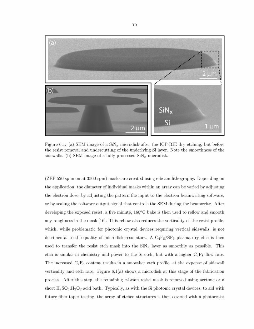
75
2 μm
1 μm2 μm
(a)
(b)
SiNx
Si
Figure 6.1: (a) SEM image of a SiNx microdisk after the ICP-RIE dry etching, but beforethe resist removal and undercutting of the underlying Si layer. Note the smoothness of thesidewalls. (b) SEM image of a fully processed SiNx microdisk.
(ZEP 520 spun on at 3500 rpm) masks are created using e-beam lithography. Depending on
the application, the diameter of individual masks within an array can be varied by adjusting
the electron dose, by adjusting the pattern file input to the electron beamwriting software,
or by scaling the software output signal that controls the SEM during the beamwrite. After
developing the exposed resist, a five minute, 160oC bake is then used to reflow and smooth
any roughness in the mask [16]. This reflow also reduces the verticality of the resist profile,
which, while problematic for photonic crystal devices requiring vertical sidewalls, is not
detrimental to the quality of microdisk resonators. A C4F8/SF6 plasma dry etch is then
used to transfer the resist etch mask into the SiNx layer as smoothly as possible. This
etch is similar in chemistry and power to the Si etch, but with a higher C4F8 flow rate.
The increased C4F8 content results in a smoother etch profile, at the expense of sidewall
verticality and etch rate. Figure 6.1(a) shows a microdisk at this stage of the fabrication
process. After this step, the remaining e-beam resist mask is removed using acetone or a
short H2SO4:H2O2 acid bath. Typically, as with the Si photonic crystal devices, to aid with
future fiber taper testing, the array of etched structures is then covered with a photoresist

76
mask, and a long SF6 isolation etch is used to remove ∼ 10-20 μm of the surrounding
SiNx and underlying Si, leaving the etched devices on a mesa. This step is not necessary if
the devices are to be tested using a “dimpled” fiber taper [45]. Next, a heated potassium
hydroxide wet etch is used to selectively remove the underlying 〈100〉 Si substrate. This
undercut etch time is maximized, depending on the microdisk diameter, so that the SiNx
microdisks are supported by a sub-micron diameter Si pillar, as shown in Fig. 6.1(b). It is
important to minimize the size of this pillar to prevent it from overlapping with the field of
the microdisk whispering gallery modes, since Si has a higher refractive index than SiNx and
is absorbing at near-visible wavelengths, resulting in significant radiation and absorption
loss. A final cleaning step to remove organic materials from the disk surface was performed
using a H2SO4:H2O2 acid etch, followed by a short (30-60 s) dilute (20:1) HF etch to remove
any surface oxide [128].
6.2 Microdisk mode simulations
Microdisk resonators rely upon total internal reflection to support whispering gallery modes
with extremely small intrinsic radiation loss [129, 15, 44, 16, 85, 130, 14]. Although exact
analytic solutions to Maxwell’s equations for these modes cannot generally be calculated,
an approximate scalar analysis can be employed to gain insight into their properties, as
described in Refs. [16, 85]. The important result from this analysis is that the microdisk
modes can be labeled by indices {m, p, q, σ} corresponding to the azimuthal, radial, ver-
tical, and polarization quantum numbers respectively, and the field has the approximate
functional form
Ez(ρ, φ, z) = eimφψp(ρ)Zq,σ(z), (6.1)
where ρ, z, and φ are the radial, vertical, and azimuthal coordinates respectively. For
microdisks with perfect cylindrical symmetry, the azimuthal exp (imφ) dependence is exact.
The radial mode profile, ψp(ρ) is given approximately by Bessel and Hankel functions inside
and outside the disk, respectively. The vertical field dependence Zq,σ(z) is given by the mode
profiles of a two dimensional slab waveguide [3]. For σ = ±1, the field is even/odd (TE/TM-
like) about the center of the microdisk slab. In practice, the microdisk thickness is chosen
to be small enough such that only the lowest order in z (q = 1) TE and TM modes have
resonance wavelengths, λo, close to the operating wavelength, and for the remainder of the
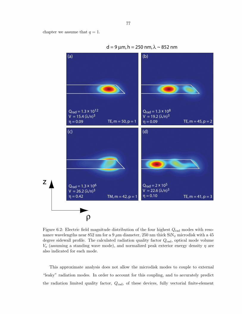
77
chapter we assume that q = 1.
(a) (b)
(c) (d)
TE, m = 50, p = 1 TE, m = 45, p = 2
TM, m = 42, p = 1 TE, m = 41, p = 3
ρ
zQrad = 2 x 10⁵
V = 22.6 (λ/n)3 η = 0.10
Qrad = 1.3 x 10⁶
V = 26.2 (λ/n)3
η = 0.42
Qrad = 1.3 x 10⁸
V = 19.2 (λ/n)3
η = 0.09
Qrad = 1.3 x 10¹²
V = 15.4 (λ/n)3
η = 0.09
d = 9 μm, h = 250 nm, λ ~ 852 nm
Figure 6.2: Electric field magnitude distribution of the four highest Qrad modes with reso-nance wavelengths near 852 nm for a 9 μm diameter, 250 nm thick SiNx microdisk with a 45degree sidewall profile. The calculated radiation quality factor Qrad, optical mode volumeVo (assuming a standing wave mode), and normalized peak exterior energy density η arealso indicated for each mode.
This approximate analysis does not allow the microdisk modes to couple to external
“leaky” radiation modes. In order to account for this coupling, and to accurately predict
the radiation limited quality factor, Qrad, of these devices, fully vectorial finite-element

78
simulations of Maxwell’s equations can be used to calculate the eigenfunctions and com-
plex eigenfrequencies of these structures. FEMLAB, a commercial software package from
Comsol, was adapted by Sean Spillane [131], and later by Matt Borselli [16, 85] and Kartik
Srinivasan [88] for this purpose.
Using this software, we modeled the microdisks described in Sec. 6.1, and studied the
properties of the whispering gallery modes supported by these devices. In addition to Qrad,
the figures of merit of particular interest are the mode volume, Vo, and the peak normalized
external energy density, η. Both Vo and η are defined in terms of the peak energy density:
Vo =∫n2(r′)E2(r′)dr′
(n2(r)E2(r)) |max=∫n2(r′)E2(r′)dr′
n2oE
2o
(6.2)
η =E2(r|n2(r) = 1)|max
(n2(r)E2(r)) |max=E2(r|n2(r) = 1)|max
n2oE
2o
(6.3)
where Eo and no are the electric field magnitude and index of refraction at the position of
maximum energy density, respectively.
6.2.1 High Q modes of 9 µm diameter microdisks at 852 nm
Figure 6.2 shows cross sections of the electric field magnitude and the relevant modal figures
of merit of the four highest Q modes supported by these devices at wavelengths within a
few nm of 852 nm. The fundamental (p = 1) TE-like mode has Qrad > 1012, indicating
that radiation is not likely to be a limiting loss mechanism for this mode in the microdisk
considered here. However, as discussed below in Sec. 6.2.2, when the disk diameter is
decreased, Qrad falls rapidly, and radiation can become the dominant loss mechanism of
these devices. Similarly, note that as the radial order p increases, m and Qrad decrease.
This is because higher radial order modes have a larger proportion of radial momentum
components, that are not bound to the microdisk volume by total internal reflection. For
the total in-plane momentum of the eigenmodes to remain invariant (for fixed {q, σ}), the
relative azimuthal (“tangential”) momentum, which is proportional to m, must decrease.
The dependence of λo and Qrad on m,n and polarization is illustrated in Fig. 6.3, which
shows that modes with larger m have higher Qrad. Nonetheless, all of the modes shown in
Fig. 6.2 have Qrad > 105.
In order to predict the interaction strength between a microcavity field and a dipole or

79
835 840 845 850 8550
2
4
6
8
10
12
Wavelength (nm)
log
10 Q
rad
m = 50m = 51
m = 45m = 46
m = 43
m = 41m = 42
m = 39 m = 38
p = 0, TE
p = 1, TE
p = 2, TE
p = 0, TM
p = 1, TM
p = 2, TM
9 μm diameter, 250 nm thickness, 45 degree sidewall
Figure 6.3: Resonance wavelength and Qrad of the lowest radial order (highest m and Qrad)modes with resonance wavelengths near 852 nm for a 9 μm diameter, 250 nm thick SiNx
microdisk with a 45 degree sidewall profile.
other perturbation within its near field, it is necessary to calculate the per photon electric
field envelope. In general, since the time averaged energy stored by the electric field of
a single photon is �ω/2 (the magnetic field stores another �ω/2 of energy), the spatially
varying single photon electric field amplitude for a given microcavity mode can be written
as:
E(r) =
√�ω
2εon2(r)Vr(r)(6.4)
where Vr(r) is a generalized position dependent mode volume, and is given by
Vr(r) =∫n2(r′)E2(r′)dr′
n2(r)E2(r)=
n2oE
2o
n2(r)E2(r)Vo. (6.5)
For many applications it is also often convenient to define an “exterior” mode volume, which
is determined by the maximum field strength outside of the microdisk, and is given in terms

80
of η and Vo by
Ve =1ηVo, (6.6)
so that the maximum field strength outside of the microdisk is given by
Ee =√
�ω
2εoVe. (6.7)
TE vs. TM: mode volume
Of the high-Q modes shown in Fig. 6.2, one is dominantly TM polarized. Although this
mode has a relatively low Qrad compared to the fundamental TE mode, it is potentially
useful for applications that place a premium on maximizing the field strength near the
surface, since the electric field exterior to the microdisk is larger for this mode compared
to the fundamental TE-like mode. Comparing the “exterior” mode volumes of the TE and
TM p = 1 modes,V TM
e
V TEe
=ηTE
ηTM
V TMo
V TEo
. (6.8)
For the values of η and Vo given in Fig. 6.2(a) and 6.2(c), Eq. 6.8 gives,
V TMe
V TEe
∼ 0.38, (6.9)
confirming that although Vo of the TE mode is smaller than that of the corresponding TM
mode, the maximum local field outside the microdisk is more intense for the TM mode
than for the TE mode. Because of this, depending on the requirements placed on Q, the
TM mode may be suited for applications studying coupling between the cavity field and
emitters located on or near the surface of these microdisks.
6.2.2 Scaling of Qrad and V with microdisk diameter
As shown in Fig. 6.4, FEM simulations were also used to calculate the variation in Qrad, Vo,
and Ve of the fundamental (p = 1) TE and TM modes as a function of microdisk diameter,
d. The microdisk thickness, h, was fixed at 250 nm for these simulations, as this is the
thickness of our commercially purchased LPCVD SiNx films. As a result, the microdisk
is not scaled isotropically when d is varied, and Qrad and Vo are not independent of λ for
a given λ/d. For the simulations presented here, we considered λ ∼ 852 nm and 637 nm,
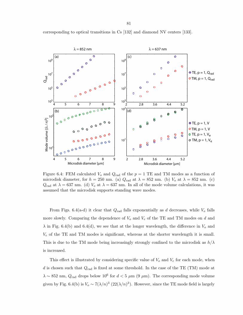
81
corresponding to optical transitions in Cs [132] and diamond NV centers [133].
105
107
109
Qra
d
4 5 6 7 8 9Microdisk diameter [μm]
103
Mo
de
volu
me
[(λ
/ n
)3]
2 3.62.8 4.4 5.2Microdisk diameter [μm]
(b)
(a)
(d)
(c)
101
102
TE, p = 1, V
TM, p = 1, V
TM, p = 1, Ve
λ = 852 nm λ = 637 nm
4 5 6 7 8 9 2 3.62.8 4.4 5.2
TE, p = 1, Ve
TE, p = 1, Qrad
TM, p = 1, Qrad
105
107
109
103
101
102
Figure 6.4: FEM calculated Vo and Qrad of the p = 1 TE and TM modes as a function ofmicrodisk diameter, for h = 250 nm. (a) Qrad at λ = 852 nm. (b) Vo at λ = 852 nm. (c)Qrad at λ = 637 nm. (d) Vo at λ = 637 nm. In all of the mode volume calculations, it wasassumed that the microdisk supports standing wave modes.
From Figs. 6.4(a-d) it clear that Qrad falls exponentially as d decreases, while Vo falls
more slowly. Comparing the dependence of Vo and Ve of the TE and TM modes on d and
λ in Fig. 6.4(b) and 6.4(d), we see that at the longer wavelength, the difference in Vo and
Ve of the TE and TM modes is significant, whereas at the shorter wavelength it is small.
This is due to the TM mode being increasingly strongly confined to the microdisk as h/λ
is increased.
This effect is illustrated by considering specific value of Vo and Ve for each mode, when
d is chosen such that Qrad is fixed at some threshold. In the case of the TE (TM) mode at
λ ∼ 852 nm, Qrad drops below 106 for d < 5 μm (9 μm). The corresponding mode volume
given by Fig. 6.4(b) is Vo ∼ 7(λ/n)3 (22(λ/n)3). However, since the TE mode field is largely

82
confined inside the microdisk, while the TM mode has field maxima close to the surface of
the disk, the exterior mode volume for Qrad ∼ 106 of the TE mode is larger than that of
the TM mode: Ve ∼ 75(λ/n)3 for the TE mode, while Ve ∼ 60(λ/n)3 for the TM mode. At
λ ∼ 637 nm, for the TE (TM) mode, from Figs. 6.4(c,d), Qrad drops below 106 for d < 3.2
μm (4.0 μm), where Vo ∼ 6.5(λ/n)3 (10(λ/n)3). In this case, the exterior mode volume,
Ve ∼, 35(λ/n)3 of the TE mode is smaller than Ve ∼ 55(λ/n)3 of the TM mode.
6.3 Microdisk testing using a fiber taper
As with the photonic crystal devices studied in Ch. 4, fiber tapers can be used to excite
optical resonances in microdisks [42, 15, 44, 43, 84]. When a fiber taper is placed within
the near field of the microdisk, as illustrated in Fig. 6.5(a), efficient coherent fiber-cavity
power transfer can be realized. In this section, fiber tapers are used to efficiently couple
light into and characterize the LPCVD SiNx microdisks described above.
γi
γ eFiber taper
Microdisk
β γi(a) (b)
γ eγ e
γ e
ts
s
t
Figure 6.5: (a) Schematic of fiber taper coupling to a microdisk traveling wave mode. (b)Generalization of the coupling process depicted in (a) to represent a microdisk that supportsstanding wave modes. s and t are the input and output field amplitudes of the fiber taperfield, respectively (see Ch. 8).
6.3.1 Waveguide microdisk coupling
This section gives a brief overview of waveguide-microdisk coupling basics, sharing similar
notation as used in Sec. 3.1 and Ch. 8. Derivations of the basic equations presented below
can be found in a number of references, including [89, 134, 135, 84, 85, 88], and Ch. 8 of
this thesis.

83
As indicated in Fig. 6.5(b), the fiber-microdisk coupling is characterized by coupling
rate γe0. Phase matching between the fiber taper mode and the whispering gallery mode
plays an important role in the determining the magnitude of γe0, and the degree of phase
matching can vary considerably depending on the refractive index and the thickness of the
microdisk, as well as on the m number of a given microdisk mode [85]. Generally, the fiber
couples preferentially to co-propagating traveling wave microdisk modes. The transmission
through the fiber taper in this case is similar to Eq. 3.3 for the waveguide coupled PC cavity
response, and is given on resonance by
To(ωo) =(1 −K)2
(1 +K)2, (6.10)
where
K =γe
0
γi +∑
j �=0 γej
. (6.11)
In the limit that there is no parasitic loss, K → γe0/γ
i, and critical coupling (K = 1, To = 0)
can be achieved when γe0 = γi [43]. Off-resonance, the transmission is given by
T (ω) = 1 − 4K(1 +K)2
(γt/2)2
(ω − ωo)2 + (γt/2)2. (6.12)
where γt = γi +∑
j γej .
In practice, for imperfectly smooth microdisks, the degenerate (±m) clockwise and
counter-clockwise traveling wave modes are coupled within the microdisk at a rate, β, due
to surface roughness induced coherent backscattering [15, 136, 44, 16]. The coupled modes
are standing wave superpositions of the clockwise and counter-clockwise traveling wave
modes, and have renormalized eigenfrequencies, ωo ±β. In the regime that β � γt, the two
standing wave modes, treated individually, accurately describe the microcavity response.
In this limit, the on-resonance transmission for each of these modes is again given by
To(ωo ± β) =(1 −K)2
(1 +K)2. (6.13)
However, since standing wave modes couple equally to each of the forward and backward
propagating waveguide modes1, in the limit that there is no additional parasitic loss K →
1In the same way as side-coupled photonic crystal cavities [83].

84
γe0/(γ
i + γe0) < 1, and To = 0 can never be achieved.
6.3.2 Microdisk testing at 852 nm
In order to characterize the microdisk resonances at 852 nm, near the D2 transition of Cs,
a swept wavelength source (New Focus Velocity) covering the 840-856 nm wavelength band
was coupled into the fiber taper waveguide, and the transmission spectra was measured for
varying fiber taper position relative to the fabricated microdisks. Figure 6.6 shows a typical
spectra when the fiber taper is positioned such that it is significantly loading the cavity.
In this wide wavelength spectrum, obtained by using a DC motor to scan the external
grating of the diode laser, at four resonant wavelengths a significant fraction of the power
in the fiber taper is dropped into the cavity. As indicated in the figure, these resonances
correspond to the TE-like microdisk modes discussed in Sec. 6.2. The different coupling
depth and linewidth of each mode is due to differences in their γi and γej , and, as a result,
K and γt.
840 845 850 855
1.0
0.8
0.6
0.4
0.2
0
Tran
smis
sio
n
Wavelength (nm)
m = 50n = 1
m = 45n = 2
m = 41n = 3
m = 46n = 2
Figure 6.6: Taper transmission when the taper is aligned close the perimeter of a 9 μmdiameter microdisk. This wide wavelength scan was obtained by performing a DC motorsweep of the laser diode grating position. This data shows a typical “family” of microdiskmodes. The high frequency noise on the off-resonance background is due to etalon effectsin the laser.

85
854.254 854.256 854.258 854.260 854.262Wavelength (nm)
1.0
0.8
0.6
0.4
0.2
0
Q ~ 3.5 x 10⁶
Q ~ 1.8 x 10⁶
Tran
smis
sio
n
(b)
Q ~ 3.1 x 10⁶
Q ~ 1.2 x 10⁶
1.0
0.8
0.6
0.4
0.2
0851.930 851.935 851.940 851.945 851.950
Wavelength (nm)
(a)
847.345 847.35 847.355 847.36 847.365
Q ~ 1.5 x 10⁶
Q ~ 1.6 x 10⁶
Q ~ 0.6 x 10⁶
(c)
Wavelength (nm)
1.0
0.8
0.6
0.4
0.2
0
Figure 6.7: Fiber taper transmission when the taper is positioned in the near field of a9 μm diameter microdisk, for two fiber taper positions. The data in (a), (b), and (c) are fordifferent nominally identical microdisks fabricated simultaneously on the same chip. Thered lines are fits using a model that includes coupling between the microdisk and the tapers,as well as between traveling wave modes of the microdisk.
Figure 6.7 shows typical narrow range wavelength scans, obtained by using a piezo to
scan the external grating of the diode laser, of the lowest radial order (p = 1) TE-like mode of
three 9 μm diameter SiNx microdisks, for varying taper positions. When the taper is weakly
coupled to the microdisk, the resonances in Fig. 6.7 have linewidths, δλo, ranging between
0.26-0.56 pm, corresponding to intrinsic quality factors Q = 1.5 × 10⁶ − 3.5 × 10⁶. From
Fig. 6.6(a), the free spectral range between modes of the same radial order but different
azimuthal number (m) was measured to be 5.44 THz (13 nm), resulting in a finesse of

86
F = 5 × 10⁴ for the fundamental p = 1 mode measured in Fig. 6.7(a). The doublet
structure in the transmission spectra is due to mode-coupling between the clockwise and
counter-clockwise modes of the disk due to surface roughness induced backscattering, as
described above. For these devices, as well as other microdisks from the same sample, the
splitting between resonances varies between Δλ = 0.5-12 pm, and no correlation between
δλo and Δλ is observed. When the taper is positioned more closely (∼ 200 nm) to the
microdisk so that the on-resonance transmission decreases, the loaded Q decreased non-
ideally. Although the degree of non-ideal loading depends on the taper diameter, as does
the coupling strength, the loaded resonances in Fig. 6.7(a-c) are typical, with I ∼ 0.4-0.6
for K ∼ 0.25-0.6, corresponding to 65%-95% input coupling efficiency from the fiber taper,
and 20% − 40% collection efficiency into the fiber taper. Reaching critical coupling, where
To = 0, is increasingly difficult and non-ideal as Δλ increases. However, for microdisks
supporting resonances with low intrinsic splitting, such as that shown in Fig. 6.7(c), it is
possible to approach To = 0 for loaded Q ∼ 8 × 10⁵.
Comparing the measured values of Q ∼ 106 for the fundamental p = 1 mode presented
here with the FEM simulated radiation loss (Qrad = 1012) results in Sec. 6.2.1, it is clear
that the measured values are not radiation limited. Tests of less surface sensitive, larger di-
ameter microdisks showed similar or reduced doublet splitting but no reduction in linewidth,
indicating that Q is most likely limited by material absorption and not surface roughness
[16].
6.3.3 Comparison with PECVD microdisks
The first SiNx microdisks fabricated in our lab were made from “home-grown” PECVD
deposited films. The processing of these device is identical to that of the LPCVD microdisks,
with the exception that PECVD SiNx is etched approximately twice as fast by the ICP-
RIE dry etch as the LPCVD material, somewhat reducing the difficulty of the fabrication.
However, PECVD SiNx has a much higher impurity density (primarily H2), and generally
has higher optical absorption [127]. Devices fabricated from this material typically had
Q ∼ 3 × 10⁵ for wavelengths in the 852 nm range. Tests of larger microdisks at 1550 nm
had similar results. However, it was observed that by annealing the microdisks at 900oC
temperatures, the quality of the material could be improved dramatically, andQ > 106 could
be observed in the 1550 nm range. Not surprisingly, the annealed PECVD material has

87
similar dry etching characteristics as the LPCVD material. A shortcut to fabricating high
quality devices without etching the “hard” LPCVD material is to anneal devices initially
fabricated from “soft” PECVD SiNx. This is not necessary for the microdisks studied here,
but may be useful for fabricating photonic crystal devices in the future.
6.4 Resonance wavelength positioning
Using the above fabrication procedure, the resonance wavelength of the microdisk modes
could be positioned with an accuracy of ±0.5 nm. In order to finely tune λo into alignment
with the D2 atomic Cs transition, or any other wavelength of interest, a series of timed
etches in 20:1 diluted H2O:49% HF solution can be employed [116, 137, 138]. As the HF
slowly etches the SiNx, the resonance wavelength of the high-Q, 9 μm diameter disk modes
was observed to blue shift at a rate of 1.1 nm/min (Fig. 6.8(a)). With this technique, the
cavity resonance could be positioned with an accuracy of ±0.05 nm without degrading the
Q factor (Figs. 6.8(b,c)). Further fine tuning can be accomplished by heating and cooling
of the sample; a temperature dependence of dλo/dT ∼ 0.012 nm/oC was measured for the
p = 1, TE-like microdisk modes.
dλ / dt = -1.14 nm / min
0 2 4 6 8 10 12
λ o (n
m)
862
858
854
852.389 852.393 852.397
Wavelength (nm)
1.0
0.9
853.355 853.359 853.363
1.0
0.9
Q ~ 3.2 x 10⁶
Q ~ 3.6 x 10⁶
Before HF etch
After 60s HF etch
λo ~ 853.36 nm
λo ~ 852.39 nm
(a) (b)
(c)
Tran
smis
sio
nTr
ansm
issi
on
HF etch time (min)
Figure 6.8: (a) Shift in resonance wavelength as a function of HF dip time. Resonancelineshape (b) before, and (c) after a 60 s HF dip. Note that the Q of the resonance has notdegraded.
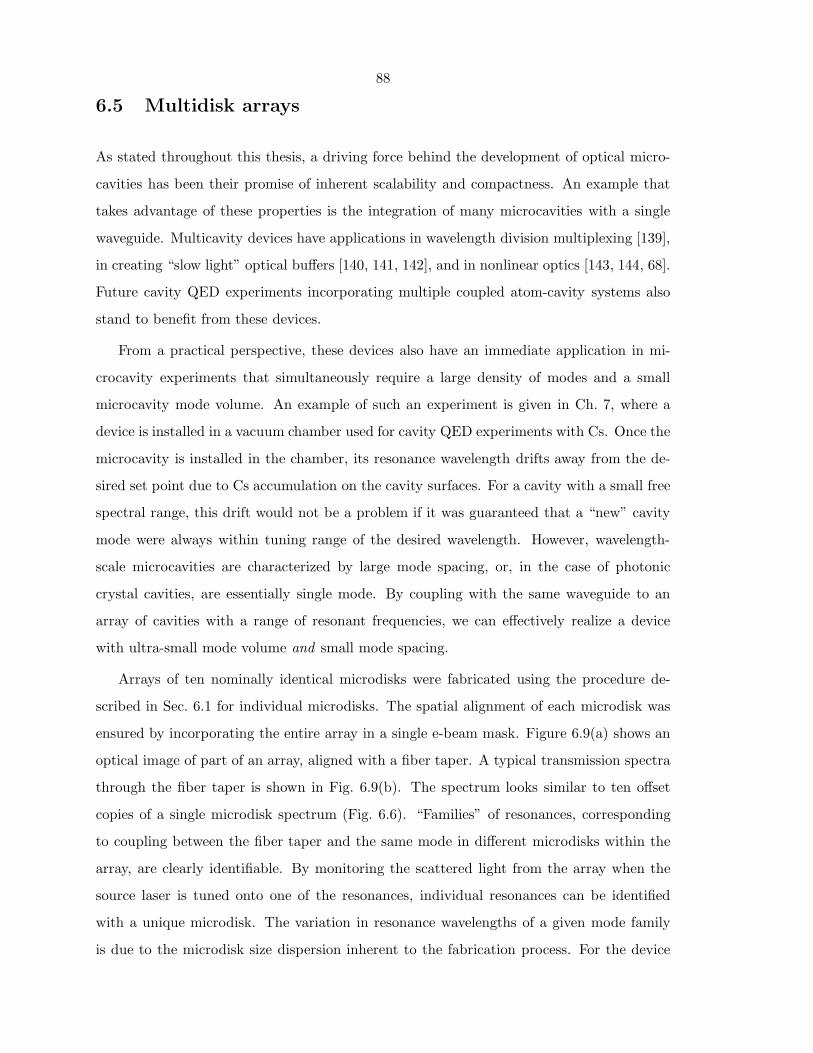
88
6.5 Multidisk arrays
As stated throughout this thesis, a driving force behind the development of optical micro-
cavities has been their promise of inherent scalability and compactness. An example that
takes advantage of these properties is the integration of many microcavities with a single
waveguide. Multicavity devices have applications in wavelength division multiplexing [139],
in creating “slow light” optical buffers [140, 141, 142], and in nonlinear optics [143, 144, 68].
Future cavity QED experiments incorporating multiple coupled atom-cavity systems also
stand to benefit from these devices.
From a practical perspective, these devices also have an immediate application in mi-
crocavity experiments that simultaneously require a large density of modes and a small
microcavity mode volume. An example of such an experiment is given in Ch. 7, where a
device is installed in a vacuum chamber used for cavity QED experiments with Cs. Once the
microcavity is installed in the chamber, its resonance wavelength drifts away from the de-
sired set point due to Cs accumulation on the cavity surfaces. For a cavity with a small free
spectral range, this drift would not be a problem if it was guaranteed that a “new” cavity
mode were always within tuning range of the desired wavelength. However, wavelength-
scale microcavities are characterized by large mode spacing, or, in the case of photonic
crystal cavities, are essentially single mode. By coupling with the same waveguide to an
array of cavities with a range of resonant frequencies, we can effectively realize a device
with ultra-small mode volume and small mode spacing.
Arrays of ten nominally identical microdisks were fabricated using the procedure de-
scribed in Sec. 6.1 for individual microdisks. The spatial alignment of each microdisk was
ensured by incorporating the entire array in a single e-beam mask. Figure 6.9(a) shows an
optical image of part of an array, aligned with a fiber taper. A typical transmission spectra
through the fiber taper is shown in Fig. 6.9(b). The spectrum looks similar to ten offset
copies of a single microdisk spectrum (Fig. 6.6). “Families” of resonances, corresponding
to coupling between the fiber taper and the same mode in different microdisks within the
array, are clearly identifiable. By monitoring the scattered light from the array when the
source laser is tuned onto one of the resonances, individual resonances can be identified
with a unique microdisk. The variation in resonance wavelengths of a given mode family
is due to the microdisk size dispersion inherent to the fabrication process. For the device

89
840 842 844 846 848 850 852 854
1.0
0.8
0.6
0.4
0.2
0
Wavelength (nm)
Tran
smis
sio
n
Fibertaper
Microdisk
(a) (a)
Figure 6.9: (a) Optical microscope image of part of an array of 10 microdisks, aligned witha fiber taper. (b) Transmission spectra of the fiber taper when it is aligned with an arrayof 10 microdisks.
tested here, the set of resonance wavelengths of a given mode varies over Δλo ∼ 0.5-1.0 nm,
and typical spacing between resonances is ∼ 0.1 nm, corresponding to ΔT < 10oC of
temperature tuning. Larger variation can be realized by slightly adjusting the microdisk
diameter in the e-beam mask definition. The broad resonance features in Fig. 6.9(b) are
a result of coupling to low-Q microdisk modes; that then bleed together, forming a broad
“coupled-cavity” resonant feature.
The maximum number of microdisks that can be incorporated in an array is currently
limited by the field of view of the SEM. If a dedicated beamwriter (as opposed to our
modified SEM) with stitching capabilities were used, larger arrays could be fabricated.
Also, the larger write speeds and better beamcurrent stability attainable with dedicated
beamwriters would possibly reduce the size dispersion of the microdisks, enabling the precise
spectral alignment of resonances required for slow-light experiments.

90
6.6 Predicted microdisk cavity QED parameters
As we are particularly interested in studying interactions between the microcavity field and
single atoms or solid state quantum emitters, it is useful to calculate expected parameters
governing the dynamics of cavity-QED systems [5, 4] employing the devices discussed above.
The key physical parameters are the cavity field decoherence rate, κ; the atom-photon inter-
action rate, g; and the atomic decoherence rate, γa = γsp+γnr, where γsp is the spontaneous
emission rate and γnr is the non-radiative decoherence rate. The atomic decoherence rate,
γa, is a property of the quantum emitter of interest, and the cavity field decoherence rate
is determined entirely by the cavity quality factor, Q:
κ =ωo
2Q=γt
2. (6.14)
The single photon coupling rate, g, depends on both the local cavity field strength, and the
dipole moment of the quantum emitter. In general, g can be written in terms of the electric
field, E, and dipole moment, d:
g(r) =〈E(r) · d〉12
�=
E(r) · d12
�=ζE(r)d12
�(6.15)
where d12 = 〈d〉12 is the dipole matrix element connecting the excited and ground state
eigenfunctions of the atom-like system of interest, and ζ is determined by the polarization
of E relative to d12. We take ζ = 1 in the following.
For a single photon confined to a microcavity, the local field strength can be written in
terms of a position dependent mode volume, Vr, as in Eq. 6.4. Although d12 is tabulated for
some atoms and solid state emitters of interest, it is often more convenient to express d12
in terms of the more routinely measured spontaneous emission lifetime, τ . From quantum
mechanical perturbation theory, it can be shown [145] that τ (measured in volume V with
index of refraction ne), is given by
1τ
=2π�2
|Ed12|2ω2n3
eV
3π2c3. (6.16)

91
Substituting for the single photon field strength,
E =
√�ω
2εon2eV
, (6.17)
gives an expression for d12 in terms of τ :
d12 =
√3πεoc3�
τneω3. (6.18)
Using Eqs. 6.4 and 6.15, g can be written in terms of τ and the cavity mode volume:
g(r) =
√3πc3
2τneω2n2(r)V (r)=
12
√3cλ2
2πτnen2(r)V (r). (6.19)
In the case of an emitter placed inside the microdisk (e.g., an embedded quantum dot), the
maximum interaction rate, assuming the emitter in aligned with the field maxima, is
go =12
√3cλ2
2πτnen2oVo
. (6.20)
When the emitter is placed at the field maxima exterior of the cavity (e.g., in the case of a
neutral atom or nanocrystal near the surface of the cavity), the interaction rate is given by
ge =12
√3cλ2
2πτneVe=
√η
2
√3cλ2
2πτneVo. (6.21)
Two regions of parameter space of particular interest in cavity QED experiments are
the strong-coupling regime and the bad-cavity regime. The strong-coupling criterion is
satisfied when the atom-photon coupling rate exceeds the decoherence rates of the system:
g � [κ, γa]. In this regime, energy can be coherently exchanged between the atom and
the cavity mode, and the system can be approximated by the dressed-state solutions of
the Jaynes-Cummings Hamiltonian [146]. The bad cavity limit is realized when the cavity
decay rate exceeds the atom-photon interaction rate, but the Purcell enhanced [147] atomic
radiative decay rate into the cavity mode exceeds the free space atomic decoherence rate:
κ � g2/κ � γa. In both of these regimes, the atom decays predominantly into the cavity
mode, permitting efficient photon collection. In practice, g2e/κγa > 1 and ge/max [κ, γa] > 1

92
are useful criteria for determining whether the Q and V of a given microdisk will permit
it to operate in the bad cavity or strong-coupling regimes when interacting with a given
quantum emitter.
6.6.1 Cavity QED with Cs atoms
The 62S1/2 → 62P3/2 (D2) hyperfine transitions of atomic Cs occur at wavelengths centered
around λCs = 852.34 nm, and the excited states have spontaneous emission lifetimes of
2π/γsp = τ ∼ 30 ns [132]. There is no non-radiative decay of excited D2 states in atomic
Cs, so γa = γsp. Figures 6.10(a) and 6.10(b) show the predicted values of κ and ge for the
fundamental TE-like and TM-like microdisk modes simulated in Sec. 6.2 at λCs, as well as
γsp. Equation 6.21 was used to calculate ge using the Ve values from Sec. 6.2.2 and the value
for τ given above (with ne = 1). The cavity decay rate was calculated assuming that the
cavity Q is limited to 4×10⁶, as per the measurements in Sec. 6.3. For microdisk diameters
with simulated Qrad < 4 × 10⁶, it was assumed that Q = Qrad, i.e., material losses were
neglected. The validity of this assumption is discussed in Sec. 6.6.3.
Encouragingly, for the TE-like fundamental mode, we can see from Fig. 6.10(a) that
ge/2π associated with these microdisk modes can approach 2 GHz with a radiation limited
κ ∼ 0.1 GHz. In particular, ge/2π ∼ 1.3 GHz is expected for the p = 1 TE mode of the
9 μm diameter microdisks studied experimentally in Sec. 6.3.2; this was measured to have
κ/2π ∼ 0.05 GHz. By reducing the diameter of the microdisk, it is possible to increase
ge/2π to 1.8 GHz without radiation loss degrading Q below this value. Clearly, this cavity
should be able to operate in the strong-coupling regime when interacting with a single
Cs atom. This is illustrated in Fig. 6.10(c), which shows ge/max [κ, γsp] as a function
of microdisk diameter. For the experimentally demonstrated 9 μm diameter microdisks,
ge/max [κ, γsp] > 25, and could increase further for smaller microdisks. Additionally, as
shown in Fig. 6.10(d), the bad-cavity parameter, g2e/κγsp > 103, indicating that the cavity
will serve as an extremely efficient photon collector, even with a significant degradation in
κ.
For a given microdisk diameter, the p = 1 TM-like mode has slightly larger ge than the
TE-like mode; however, κ becomes radiation limited for much larger diameter microdisks
than does the TE-like mode. Nonetheless, it should also be possible to reach the strong-
coupling regime with this mode.

93
0
400
800
1200
1600
2000
0
10
20
30
40
3 5 7 94 6 8
ge2
/ κ
γ sp
Microdisk diameter [μm]
TE, p = 1
TM, p = 1
6.4 8.07.2 8.8Microdisk diameter [μm]
5.6
[GH
z ]
0.01
100
10
1
0.1
[GH
z ]
0.01
10
1
0.1
5 7 94 6 8Microdisk diameter [μm]
κge
γsp
5 7 94 6 8Microdisk diameter [μm]
ge
/ m
ax[κ
, γ s
p ] TE, p = 1
TM, p = 1
(a) (b)
(d)(c)
λ = 852 nm
κge
γsp
Figure 6.10: Cavity QED parameters for a Cs atom in the microdisk near field, as a functionof microdisk diameter. The Cs atom is taken to be at the field maximum outside of themicrodisk. The microdisk thickness is h = 250 nm, and λ ∼ 852 nm. In calculating κ,Q = min
[4 × 10⁶, Qrad
]. (a,b) Interaction and decoherence rates for the fundamental (a)
TE mode, (b) TM mode. (c) Strong-coupling parameter. (d) Bad cavity parameter.
6.6.2 Cavity QED with diamond NV centers
Single nitrogen-vacancy (NV) defects [133] in diamond share many properties associated
with atomic systems. Namely, they emit single (non-classical) photons at well defined
wavelengths [148], and have relatively large dipole moments. The NV defect center, formed
by an N substitutional defect adjacent to an empty lattice site, has attracted significant
interest because it is relatively abundant in most diamond samples, it emits photons in the
easily detectable visible wavelength band (λNV ∼ 637 nm), and it can be varied in density by
subjecting the sample to MeV electron irradiation in order to damage the diamond lattice

94
and create vacancies. By forming the NV centers in diamond nanocrystals [149], it should
be possible to place these “artificial atoms” within the near field of the SiNx microcavities
discussed here.
An analysis identical to that used above with Cs atoms can be applied to predict the
cavity QED parameters when the microdisk interacts with an NV center. Although NV
centers have a spontaneous emission lifetime of 2π/γsp = τ ∼ 12 ns [150] when formed in
bulk diamond, and 2π/γsp = τ ∼ 20 ns when formed in diamond nanocrystals [149], at room
temperature, γnr in NV centers is very large due to coupling with phonons. At liquid-He
temperatures (2 K), γa/2π as low as 13 MHz has been measured [151] in bulk diamond, but
results vary, depending on material quality. In the following, we take γa = γsp = 2π/20 ns−1.
Figures 6.11(a) and 6.11(b) compare γsp with the predicted values for ge and κ for the
TE- and TM-like p = 1 modes at λ ∼ 637 nm of the microdisks simulated in Sec. 6.2.2, as
a function of microdisk diameter. For both the TE- and TM-like modes, ge = 2-3 GHz is
predicted before the microdisk becomes radiation limited, and Q < 4× 10⁶ (κ > 0.1 GHz).
As shown in Fig. 6.11(c), the coupled NV-center cavity system should be able to reach the
regime of strong-coupling, with ge/κ > 20. In Fig. 6.11(d), the bad cavity factor, g2e/κγsp,
exceeds 103. This factor is of particular importance when considering NV-centers or other
solid-state emitters with potentially large γnr, as it indicates how large γa can be with the
system remaining in the bad-cavity regime. For g2e/κγsp = 103, the system can tolerate
γa ∼ 103γsp ∼ 50 GHz while remaining in the bad cavity regime. Finally, note that at this
wavelength the TM-like mode performs equally, if not better, than the TE-like mode.
6.6.3 Practical limitations
The above analysis assumes that the cavity Q is limited by either material or radiation
loss. In practice, effects such as surface roughness and surface state absorption can become
the dominant microcavity loss channels [16]. Although experimental evidence in Sec. 6.2.1
indicates that this was not the case for the microdisks studied there, surface effects be-
come increasingly pronounced as the microdisk diameter shrinks and the field becomes less
confined. Similarly, the TM-like mode is a comparatively better sensor of the microdisk
surface than is the TE-like mode, and is more sensitive to surface related loss mechanisms.
Further systematic experimental studies of Q vs. microdisk diameter and mode polarization
are needed to better understand the impact of these effects.

95
0
400
800
1200
0
5
10
15
20
25
2 4 6 73 5
ge2
/ κ
γ sp
Microdisk diameter [μm]
TE, p = 1
TM, p = 1
3.6 5.24.4Microdisk diameter [μm]
2.8
[GH
z ]
0.01
100
10
1
0.1
[GH
z ]
Microdisk diameter [μm]
κge
γsp
3 52 4 6Microdisk diameter [μm]
ge
/ m
ax[κ
, γ s
p ]
TE, p = 1
TM, p = 1
(a) (b)
(d)(c)
0.01
100
10
1
0.1
3 52 4 6
TE, p = 1 TM, p = 1
λ = 637 nm
30
κge
γsp
Figure 6.11: Cavity QED parameters for an diamond NV center interacting with the mi-crodisk near field, as a function of microdisk diameter. The NV center is taken to be atthe field maximum outside of the microdisk. The microdisk thickness is h = 250 nm, andλ ∼ 637 nm. In calculating κ, Q = min
[4 × 10⁶, Qrad
]. (a,b) Interaction and decoherence
rates for the fundamental (a) TE mode, (b) TM mode. (c) Strong coupling parameter. (d)Bad cavity parameter.
Wavelength dependent material absorption was also ignored in the analysis of the mi-
crodisk modes at 637 nm. A difference in the intrinsic material optical loss rate at 637 nm
compared with that at 852 nm would modify the maximum obtainable Q for devices in
this wavelength range. However, based on existing literature [119, 118], we expect the
optical attenuation coefficient of SiNx to fall within the same order of magnitude at both
wavelengths.

96
6.7 Conclusion
In this chapter, we have shown that microdisk optical cavities fabricated from SiNx have
sufficiently low optical loss rates and sufficiently large single photon peak field strengths
for cavity QED experiments with Cs atoms operating within the strong-coupling regime.
These cavities should allow GHz atom-photon coupling rates, which are higher than any
other high-Q microcavity operating at λ = 852 nm demonstrated to date. Because of the
low optical loss of SiNx in the visible wavelength range, these cavities should also be useful
for experiments studying a wide class of solid state quantum emitters, such as diamond
NV centers. Ultimately, by taking advantage of the planar, CMOS compatible nature of
the SiNx material system, fully integrated photonic chips for visible wavelengths, consisting
of many cavities connected through on-chip waveguides, can be designed and fabricated.
In the next chapter, we will show how these devices can be integrated with atom chips,
eventually promising fully “on-chip” cavity QED and quantum information processing with
neutral atoms.

97
Chapter 7
An atom-cavity chip
Atom chips [152, 50, 51, 153] have rapidly evolved over the last decade as a valuable tool in
experiments involving the cooling, trapping, and transport of ultra-cold neutral atom clouds.
Fabricated using standard semiconductor processing techniques, atom chips are formed by
conducting microwires lithographically patterned on a planar insulating substrate. For
modest microwire currents, extremely high magnetic field gradients can be formed close to
the atom chip surface [154], and by combining appropriate microwire configurations with
externally generated magnetic bias fields, magnetic traps for cold atoms can be realized
[155, 156, 157]. Crucially, the position of the magnetic trap, and hence the atoms, can be
moved dynamically by varying the current through the microwire configuration.
Examples of experiments that leverage the planar, scalable, micron-sized features of
atom chips include studies of Bose-Einstein condensates [158, 159] and degenerate Fermi
gases [160] “on-chip”, “portable” Bose-Einstein condensates [161], atom waveguides [162]
and conveyer belts [163], and atom interferometers [164, 165, 166, 167]. The field of
cavity QED [6, 5, 4] and, in particular, cavity QED with neutral atoms and micropho-
tonic devices [168, 169, 170, 171, 172, 173, 131, 29] is poised to significantly benefit from
atom chips. Integration of atomic and microphotonic chips [170, 173, 171, 174, 175] of-
fers several advancements to the current state-of-the-art Fabry-Perot cavity QED systems
[176, 34, 177, 178, 179], most notably a scalable platform for locally controlling multiple
quantum bits. Ultimately, the atom chip can be used to deliver and possibly trap single
atoms within the near field of a microcavity.
In this chapter, we describe and demonstrate a technique for integrating the fiber coupled
microcavities studied in previous chapters with atom chips developed by Benjamin Lev [180].
Integrated “atom-cavity” chips fabricated using this technique can be installed in atom

98
trapping vacuum systems while maintaining an efficient fiber input and output channel
between the microcavity and the outside world. By taking advantage of the small size of
the microcavities, we show that they can be directly integrated with the metal layer used
in optically and magnetically trapping atoms near the surface the atom chip, and hence,
the cavity. In Sec. 7.1, we describe the fiber mounting technique, and in Sec. 7.2 use a
fiber coupled device installed in the atom trapping UHV system to study the sensitivity of
a SiNx microdisk to a dilute cesium (Cs) vapor. In Sec. 7.3, we show how Cs atoms can be
trapped directly above an array of microdisks integrated with a mirrored surface attached
to an atom chip. Much of the work presented in Sec. 7.1 and Sec. 7.2 first appeared in Ref.
[17].
7.1 Fiber coupled microcavities for atom chips
7.1.1 Robust fiber mounting
The ability to align fiber tapers within the near fields of microcavities is crucial for estab-
lishing an efficient optical channel into and out of these devices. As described in Ch. 4 and
6, this can be achieved using computer controlled positioning stages. However, these stages
are not compatible with ultra-high vacuum (UHV) systems required for atomic physics ex-
periments. Rather than attempt to integrate vacuum-safe piezo [181] or mechanical [29]
positioning stages with the atom chip apparatus, our solution to this problem was to de-
velop a technique to permanently attach an optimally aligned fiber taper to the microcavity
chip.
A practical fiber-to-microcavity mounting technique must (i) permit high resolution
(< 100 nm) positioning of the fiber relative to the microcavity for optimal coupling, (ii) not
create significant optical loss, and (iii) be robust to any mechanical impulses imparted during
the installation of the device in the experimental apparatus. In addition, for experiments
with atom chips, the mounting technique must (iv) be UHV compatible, (v) be able to
withstand elevated temperatures (∼ 150 oC) required during vacuum chamber bakes, and
(vi) not interfere with the atom cooling and trapping optics.
The solution discussed here is to use UV curable epoxy to permanently and robustly fix
the position of a fiber taper that is initially aligned with the microcavity using computer
controlled stages. The critical features of this technique are epoxy “microjoints” that fix

99
Figure 7.1: Illustration of a fiber taper mounted in a “U” configuration to a glass slide. Thefiber taper is bonded to the glass slide using UV curable epoxy.
the position of the taper in the immediate vicinity of the microcavity, in addition to epoxy
“macrojoints” that fix the position of the fiber pig-tails relative to the atom chip. A brief
description of the mounting procedure follows.
The microcavity chip (3-5 mm × 3-8 mm × 0.3 mm) is first aligned and bonded using
polymethyl methacrylate (PMMA) to the desired location on a rigid planar substrate, which,
for the purpose of the experiments being considered here, is an atom chip. The fiber taper is
placed in a self-tensioning “U” configuration, and is bonded to and supported by a glass slide
(1 cm × 1.5 cm, ∼ 200 μm thick) as illustrated in Fig. 7.1. The top surface of the glass slide
is suctioned to a vacuum chuck that is attached to a computer controlled vertical positioning
stage. The substrate supporting the microcavity (i.e., the atom chip) is positioned on the
computer controlled horizontal positioning stage used in Ch. 4. Using these high resolution
stages, the taper is aligned with the microdisk. Adjustment in the lateral gap between the
taper and the microdisk is used to optimize the level of cavity loading. As shown in Fig. 7.2,
the fiber taper and microdisk are then permanently attached using UV curable epoxy in
two regions: (i) Microscopic glue joints between the fiber taper and lithographically defined
supports fix the position of the taper relative to the disk, and (ii) macroscopic glue joints
between the taper support slide and the atom chip fix the position of the taper support
relative to the chip and serve as stress relief points for the fiber pig-tails. The glue for each

100
10 μm
Fiber taper
Microdisk
Epoxy microjoint
Fiber taper support
Microdisk array
MOT / magnetic trap
Photonic chip
Microwire
Fiber taper support
Epoxy macrojoint
Fiber taper
Atom chip
(a)
(b)
Figure 7.2: (a) Illustration of a fiber coupled photonic chip integrated with an atom chip. (b)SEM image of a fiber taper permanently mounted to a microdisk using epoxy microjoints.
of these joints is dispensed in advance, prior to the taper alignment.
The microjoint glue (Dymax OP-4-20632) is applied to the supports using a sacrificial
fiber taper as a “brush.” When a fiber taper “brush” is dipped in epoxy, beads of glue
whose diameter are on the same order as the taper diameter are formed. These beads can
be transfered onto the supports on the optical chip by contacting the taper “brush” with the
supports using the high precision stages. Only glue with a low enough viscosity (∼ 500 cP)

101
can be transfered in this way. To minimize optical loss, it is important to minimize the
quantity of glue deposited in the anticipated bonding region. In the example shown in Fig.
7.2, the epoxy was actually deposited on the supports adjacent to the eventual bonding
region; from there it was transfered using the fiber taper that ultimately was bonded to
the chip. The macrojoint glue (Dymax OP-4-20663) is applied to the atom chip manually
using a syringe or sharp point.
The glue is cured using a UV spot lamp (Dymax BlueWave 50, 3000 mW/cm2) coupled
to a lightguide that directs the light onto the sample. The macrojoints cure after a few
seconds of direct exposure. Somewhat surprisingly, the microjoints take much longer: Typ-
ically, a cure time of at least 5 min is used. During this process, it is important that the UV
source have an unobstructed line of sight to the microjoint regions. Once the macrojoints
have cured, it is difficult to non-destructively test the strength of the microscopic joints.
Test trials with no macrojoints, in which the stages are used to raise the fiber taper to stress
the microjoints after curing, indicate that a correctly bonded microjoint will not fail before
the SiNx support breaks.
To guarantee robustness, it is important that the microcavity array be isolated on a
mesa by > 10-20 μm, as described in Ch. 4. This ensures that in the case of a mechani-
cal impulse, the fiber taper does not contact the edge of the photonic chip, which would
result in significant insertion loss. To avoid blocking trapping laser beams or obscuring
imaging, the entire fiber taper mount must lie below the plane of the optically and magnet-
ically trapped atoms (∼ 600 μm above the atom chip surface). A sufficiently low-profile is
achieved by aligning and bonding the taper support slide parallel to and below the plane of
the microcavity top surface. Geometric requirements of the trapping beams are discussed
further below.
During the taper mounting procedure, the taper-microdisk coupling is monitored by
measuring the microdisk resonance wavelength (λo) and contrast (ΔT ) through the fiber
taper, with no noticable change being observed during the curing of the epoxy joints. The
microjoints incur taper diameter dependent broadband insertion loss; approximately 10-
15% optical loss per joint is optimal. Post-cure, the fiber-cavity alignment is extremely
robust, withstanding all of the vacuum installation procedures described below.

102
7.1.2 Installation in a UHV chamber
The ultimate test of the robustness of the fiber coupled device is its installation in the
vacuum chamber used for performing atom chip trapping experiements. This installation
requires that the atom-cavity chip be transported across the Caltech campus from Oskar
Painter’s photonics lab to Hideo Mabuchi’s atomic physics lab. There, the atom chip is
mounted onto a copper chassis that also holds several wire coils used for generating the
magnetic fields required for atom trapping [180]. The chassis is then turned upside down,
so that the atom chip top surface is facing down, and installed in the vacuum chamber.
Once in the vacuum chamber, a number of wires used to pass current to the microwires
are connected to the atom chip. Vacuum-safe fiber feedthroughs [182] are used to pass the
fiber-pigtails out of the chamber. The chamber is then evacuated to the 10−3 Torr range
using a turbo pump backed by a mechanical roughing pump. Following this initial pump
down, the chamber is heated to 120 oC for 24-48 hours. During the bake, when the pressure
reaches ∼ 10−4 Torr, an ion pump is turned on. Finally, when the chamber pressure reaches
∼ 10−7 Torr, the chamber is slowly cooled to room temperature where the final chamber
pressure is typically in the 10−9 Torr range.
During this installation process the fiber coupled atom-cavity chip is manipulated sig-
nificantly, and sometimes jostled. In order to be sure that the taper-cavity coupling is not
disturbed as a result, the microcavity resonance is monitored continuously during these
procedures. For a successfully mounted device, the fiber-cavity coupling, as measured by
the fiber off-resonance transmission Toff and ΔT , is impervious to these disturbances, il-
lustrating the robustness of this technique. In fact, tests have shown that the atom-cavity
chip can be dropped centimeters onto the optical table without disturbing the coupling, so
long as the fiber taper is not contacted directly.
In contrast, the resonance wavelength λo of high-Q small V microcavities is very sensitive
to the microcavity environment, and to sub-monolayer changes to the microcavity surfaces.
In the case of the SiNx microdisks used in the experiments to date, after the initial pump
down but before the chamber bake, λo typically blue shifts by −0.1 nm. This shift is due
in part to the difference between the refractive index of air and vacuum (Δn ∼ 10−5), and
in part due to the desorption of molecules that may have accumulated on the microcavity
surface before it was installed in the vacuum chamber. As the chamber is heated during the

103
bake, the resonance shifts reversibly at a rate of ∼ 0.012 nm/oC. Additionally, while the
chamber is in steady state at an elevated temperature, λo can be observed to red-shift slowly
at a rate that depends on the recent history of the chamber. This shift, Δλo,bake ∼ 0.1−0.3
nm is not reversible, typically saturates over the course of the bake, and is presumed to
be due to contaminants on the chamber sidewalls and in the pumping system that outgas
during the bake and collect on the cavity surface.
7.2 Microcavity surface sensitivity to Cs vapor
Of significant concern is the effect of Cs and other related compounds on the optical prop-
erties of microcavities installed in the vacuum chamber. Cs and other contaminants are
introduced into the chamber from a heated Cs source (“oven”) attached to the chamber via
a UHV valve. During a typical lifetime of a microcavity installed in the UHV system, the Cs
valve is opened in two scenarios: periodically during the inital pump down and/or bake, to
equilibrate the pressure in the Cs oven with that in the chamber, and during the operation
of the atom trapping experiments in order to source the atom trap with Cs atoms. In both
scenarios, opening the Cs valve is observed to be directly correlated with a red shifting of
λo. This is problematic when using microcavities in atomic cQED experiments, where it
is required that the microcavity resonance wavelength be maintained close to that of the
atomic transition of interest. Ultra small mode volume microcavities are either single mode
(in the case of PC cavities) or have a large mode spacing (∼ 13 nm for the microdisks
studied in here and in Ch. 6). Since thermal tuning of the cavity resonance is typically
limited to ∼ 0.1− 0.2 nm, lacking another high bandwidth tuning technique, it is necessary
that Δλo be minimized and/or controlled during the experiment.
During the chamber pump-down, the most successful protocol in practice is to open the
Cs valve for ∼ 30 minutes prior to beginning the bake, and for several ∼ 10 minute intervals
during the bake, once the chamber pressure is below 10−4 Torr. This allows the Cs oven to
be “pumped on,” and maintained at a pressure close to that of the main chamber. When
the Cs valve is opened during the bake1, it is usually possible to observe a shift in λo at
rate of roughly 1-10 pm/min. In some instances, opening the Cs oven during the bake has
resulted in rapid deterioration of the microcavity resonance Q, accompanied by a rapid shift
1The Cs oven is tyically at 60 oC during the bake.

104
0
0.1
0.2
0.3
0.4
0.5
0 300
Δλo
(nm
)
t (hours cesium)200100
λo = 0.22 t 0.13
400 500
Figure 7.3: Resonance wavelength shift of the 9 μm diameter SiNx microdisk studied in Ch.6 as a function of time exposed to Cs. The Cs partial pressure was 10−9 − 10−8 Torr.
in λo. Trials indicate that initially pumping on the Cs oven at room temperature before
beginning the bake is important in order to avoid this problem.
During the operation of the experiment, it is necessary to operate the Cs oven at 40-50oC with the valve open completely in order to reach a sufficiently high Cs partial pressure
(∼ 10−8 − 10−9 Torr) in the chamber to enable formation of a relatively large MOT. Atoms
from this Cs vapor adsorb on the microcavity surface with a logarithmic time dependence,
i.e., in a “glassy” manner [183], where interactions between deposited atoms quench the
rate of adsorption. As shown in Fig. 7.3, typical “saturated” shifts in λo are Δλo,Cs ∼ 0.5
nm; however, Δλo,Cs can vary depending on the conditions of the Cs oven.
Quantitatively, a shift, Δλo, of the disk resonances can be related to a deposited surface
film of thickness, s, by
s = Δλo/(λo(nf − 1)Γ′), (7.1)
where Γ′s represents the fraction of modal energy in the film [85] and nf is the refractive
index of the film. From finite element simulations of the 9 μm diameter microdisk used in
collecting the data in Fig. 7.3, Γ′ = 0.0026 nm−1 for the p = 1 TE-like mode. Assuming a
film index of refraction equal to that of SiNx, the measured wavelength shift at the longest
measured time (t = 450 h) corresponds to roughly a half-monolayer coverage of Cs on the

105
disk surface (monolayer thickness ∼ 4 A [184]).
The time dependence of this film growth can be approximately modeled as follows.
Roughly,ds
dt= Pe−ks (7.2)
where s is the fractional number of monolayers coating the microcavity surface, P is pro-
portional to the Cs partial pressure, and k is a constant describing a repulsive interaction
between adsorbed Cs atoms. According to this model,
s(t) =ln(kPt+ c)
k, (7.3)
where c is determined by s(t = 0), and is equal to 1 for s(0) = 0. A saturated film
thickness, ssat, can be defined in terms of the rate of accumulation, s: When s is lower than
a practical threshold, ssat, changes in s (and therefore λo) can be ignored over the course
of the experiment. Using this definition, ssat is given by
ssat =1k
ln(P
ssat). (7.4)
Equation (7.4) clearly indicates that for a given ssat, ssat scales logarithmically with P .
This indicates that working in a UHV systems with a lower non-Cs background pressure,
which would enable the formation of a MOT with a similarly lower Cs partial pressure,
would reduce ssat. Ultimately, a two chamber atom trapping system, comprised of a MOT
chamber connected to a magnetic trapping chamber, could be used to significantly reduce
P in the vicinity of the microcavity.
Interestingly, assuming that the model described above is valid, this background pres-
sure dependence potentially can be exploited to semi-permanently tune a microcavity into
resonance after installing the cavity in the vacuum chamber but prior to beginning the ex-
periment. This tuning mechanism is in the spirit of work that used noble gas condensation
on low temperature semiconductor microcavities to tune their resonances [185, 186]. The
envisioned tuning procedure is illustrated in Fig. 7.4: By initially elevating the Cs partial
pressure significantly, for example, to 10Po, where Po is the normal operating Cs partial
pressure, a film of thickness � ssat|P=Po can be deposited. The Cs partial pressure can then
be reduced to Po, at which point the rate of Cs accumulation is predicted to be slow on the

106
Time [1 / Pok]
Film
th
ickn
ess
[ 1
/ k
]
P = Po
P = 10 Po
20000
3.5
Figure 7.4: Simulated accumulated Cs film thickness as a function of time for varyingbackground pressure. For the upper curve, at the time indicated by the dashed vertical linethe Cs partial pressure is reduced by an order of magnitude.
time scale of the lifetime of the experiments (ideally, hundreds of hours). In practice, exper-
imental efforts to realize this tuning have been unsuccessful, due to a tendency for the Q of
the microcavity resonance to degrade when the Cs oven is opened at elevated temperatures.
This Q degradation is not always observed (it was not noticed for the device from which
the data in Fig. 7.3 was taken), and is currently thought to be related to contamination of
the Cs oven. The use of atom “dispensers” as an alternative source of Cs [187] is currently
being investigated.
A potentially simpler alternative to the above techniques for reducing the effects of Cs
is to investigate treatments of the microcavity surface. In Ref. [188], Ghosh et al. coated
the inside surfaces of a photonic crystal fiber with an organosilane, which in combination
with light induced atomic desorption (LIAD), prevents room temperature Rubidium atoms
from interacting with the photonic crystal fiber walls. It is possible that a similar process
can be used with the microcavities studied here.

107
7.3 Atom trapping on the atom-cavity chip
Atom chips employ a combination of external optical cooling and on-chip magnetic trapping
to assemble clouds of cold atoms from a dilute thermal gas. When integrated with a fiber
coupled cavity, it is crucial that the cavity not interfere with these trapping fields, and that
the atom chip have the ability to deliver the trapped atoms to the vicinity of the cavity.
Experiments with cold atoms and Fabry-Perot cavities typically source atoms from free
space MOTs, formed far from the cavity and transfered to the cavity via either gravity
[176] or an optical potential [178]. When the cavity is integrated with an atom chip, the
atoms can be transfered from a mirror-MOT [50], formed near the surface of the atom chip,
into a purely magnetic trap, and then magnetically waveguided into the cavity [175, 173].
Compared to Fabry-Perot cavities, microcavities are a much smaller geometric obstacle. By
taking advantage of microcavities’ small size, it is possible to directly integrate them with
the atom chip, and to form a MOT within tens of microns from the cavity surface. In this
section, after a brief overview of the operation of the atom chip used in these experiments,
a fully integrated atom-cavity chip that permits trapping directly above a microdisk cavity
is presented.
7.3.1 Atom chip basics
This subsection briefly reviews the basic operation of the atom chips fabricated by Benjamin
Lev with which the microcavities were integrated. A detailed description can be found in
B. Lev’s thesis [180], and an excellent general overview of this type of atom chip is given in
Ref. [50].
Ultimately, the atom chip confines atoms within a purely magnetic trap that is formed
by a superposition of magnetic fields generated by currents in microscopic (on-chip) and
macroscopic (external) wires. An example of a canonical microwire magnetic trap is illus-
trated in Fig. 7.5(a): A two dimensional trap is formed by superimposing a homogeneous
bias field with the radially decaying field of a microwire, resulting in a field minima at a
fixed height above the wire. By dynamically varying the microwire current and the magnetic
bias field, the height of the trap above the microwire can be adjusted. Three dimensional
magnetic trapping can be achieved by breaking the translational symmetry of the wire, and
patterning “u” or “z” shaped microwires, as illustrated in Fig. 7.5(b). More complicated

108
+
Bias Microwire
=Magnetic
field
Height above wire
dB / dr ~ 10 - 1000 G / cm
Magnetic trap
(b)
(a)
Figure 7.5: (a) Illustration of a magnetic trap formed by superimposing a homogeneousmagnetic bias field with the magnetic field generated from current in a wire directed out ofthe page. This trap offers confinement in the 2D plane of the page. (b) Top view of twowire configurations that provide 3D magnetic trapping when combined with a homogeneousbias field.
microwire circuits permit the atom trap position to be adjusted in all three dimensions by
dynamically reconfiguring the current path.
However, in order to magnetically trap a significant number of atoms, it is first necessary
to cool and trap them in a MOT [189]. A generic MOT is formed when the intersection
of three sets of red-detuned counter-propagating and orthogonally polarized laser beams,
oriented along orthogonal axes, is aligned with an externally generated magnetic quadrapole
field. The surface of an atom chip cuts off optical access from the half-space below it,
necessitating the use of a “mirror-MOT”, in which a surface on the atom chip is used to
reflect a pair of orthogonal 45o beams that intersect a pair of counter-propagating beams
aligned parallel and close to the surface of the atom chip, as illustrated in Fig. 7.6. This
geometry provides three dimensional optical cooling at the point where all of the beams
intersect; when combined with a magnetic quadrapole field, this allows the formation of
a MOT. The magnetic quadrapole field can either be supplied by microwires on the atom
chip surface, or by macroscopic wires. The resulting traps are referred to as “micro mirror-
MOTs” and “macro mirror-MOTs”, respectively.
In the atom trapping apparatus used here, atoms are first collected in a macro mirror-
MOT, then transferred into a micro mirror-MOT, before undergoing optical pumping and
sub-Doppler polarization gradient cooling, and finally being transfered into a purely mag-
netic trap. A “u” shaped microwire, positioned below a mirrored region of the atom chip, is

109
σ+ σ-
σ+ σ-
MOT beams
MIrror
Microwires(a) (b)
(c)
Figure 7.6: Illustration of the laser beam and microwire geometry used to form the atomchip mirror-MOT. During the MOT formation, current flows through the “u” section of the“h” microwire circuit.
used to generate the quadrapole field for the micro mirror-MOT. After sub-Doppler cooling,
the temperature of the trapped atoms is < 10 μK, and they are optically pumped into the
mf = |l| state, where the quantization axis z is defined by a bias field. The optical fields
are then turned off, and since the potential energy of an atom in a magnetic field H is given
by
Vm(r) = −μmfHz(r), (7.5)
atoms in the mf = |l| state are trapped in magnetic field minima. If the magnetic trap
position and shape are closely matched with those of the micro mirror-MOT, and if the
sub-Doppler cooling and optical pumping are optimized, a large fraction of the atoms in
the micro mirror-MOT can be transfered into the purely magnetic trap. The magnetic trap
position can then be adjusted by dynamically varying the path of current flow through the
microwire circuit on the atom chip. Practically, the degree and extent to which this position
can be controlled is limited by the microwire geometry, the maximum current allowed by

110
the microwires, and the trap lifetime.
7.3.2 Integrating cavities with atom chips
The initial proposal in Ref. [173] to integrate microcavities with atom chips anticipated using
atom waveguiding [162, 163] to move atoms from a magnetic trap formed at the micro
mirror-MOT location to a microcavity positioned several mm away. As the experiment
progressed, however, it was realized that because of the small size of the microdisks, the
atom delivery could be simplified by initially trapping the atoms in a micro mirror-MOT
directly above the microcavity. The atoms could then be moved into the cavity near-field
from either a magnetic trap or directly from the mirror-MOT, without requiring the extra
waveguiding step. However, in order to form the initial micro mirror-MOT directly above
the cavity, it is necessary that the cavity not disrupt the mirror region. In the case of
“macroscopic” cavities, this is not possible. Conversely, the small footprint of microcavities
(1- 100 μm) has a minimal effect on the comparatively large (1 cm) MOT beams being
reflected by the mirror, and it is possible to form a mirror-MOT directly above them. As
illustrated in Fig. 7.7(d), so long as the MOT is formed at a height above the surface greater
than the microcavity footprint, it should be largely unaffected.
Implementing this experimentally requires that the cavity be integrated with the mir-
rored region of the atom chip, so that the cavity region forms a small “defect” in the
otherwise uniform mirror, and is aligned with the microwire that sets the micro mirror-
MOT position. Ultimately, this could be achieved by fabricating the cavity from the same
substrate as the atom chip, creating a monolithic atom-cavity chip. A simpler short-term
solution is illustrated in Fig. 7.7: Incorporate a mirror on the same chip as the microcavity,
and then bond the resulting cavity-mirror chip to the desired location on the independently
fabricated atom chip. Note that the fiber mounting technique described in Sec. 7.1 is com-
patible with this scheme, and that the low profile of the mounted fiber ensures that it does
not interfere with any of the optical beams.
It is straightforward to modify the fabrication process of the SiNx cavities described in
Ch. 6 to include a mirror layer. Briefly, the procedure is as follows. The lithography, dry
etching, and isolation steps are unchanged. After the isolation etch, before removing the
photoresist that masks the device mesa, an optically thin layer of gold is evaporated onto
the entire microcavity chip. A gentle acetone bath is then used to lift-off the gold coated

111
σ+ σ-
σ+ σ-
MOT beams
Cavity - mIrrorchip
Microwires
Cavity mesa
(a) (b)
(c)
(d)
Figure 7.7: Illustration of the laser beam and microwire geometry used to form a mirror-MOT when the cavity-mirror is integrated with the atom chip. (a) Top view, (b) end view,(c) side view. The zoomed-in detail (d) shows how a MOT can be formed above an array ofcavities on an otherwise uniform mirror. The shadow from the cavities only extends abovethe surface as high as the cavity footprint.
photoresist mask. This leaves the device mesa uncovered, while the rest of the chip surface
is coated with gold. The final undercutting and cleaning steps are unchanged.
A device fabricated using this process is shown in Fig. 7.8. This device consists of a
3× 10 array of 9 μm diameter SiNx microdisks that are isolated on a mesa ∼ 20 μm above
the gold coated Si substrate surface. The microdisk array dimensions are 100 μm × 100
μm, and the chip dimensions are 4 mm × 6 mm × 0.3 mm. The device was bonded to the
atom chip, as described in Sec. 7.1.1, positioned so that the microdisk array was aligned
above the “u” microwire, as illustrated in Fig. 7.7. A fiber taper was mounted to the device,
and the resulting fiber-coupled atom-cavity chip was installed in B. Lev’s atom trapping
UHV system.
Using this device, and following the MOT operation and magnetic trapping procedure
described in Ref. [180], it was confirmed that ∼ 106 Cs atoms could be trapped ∼ 200 μm

112
GOLD MIRROR
MICRODISK ARRAY
GOLD MIRROR
MICRODISK ARRAY
Figure 7.8: SEM images of a cavity-mirror chip. The mesa contains a 3 × 10 array of 9μm diameter microdisks, and is isolated by ∼ 20 μm above the surrounding gold coated Sisubstrate.
above the surface of the microdisk array in macro mirror-MOT, then transferred to a micro
mirror-MOT ∼ 100 μm above surface, and finally lowered into the device array using a
purely magnetic trap. Figure 7.9 shows fluorescence images of the laser cooled atoms being
delivered to the microcavity array in this way. The images were generated by precisely
halting the experiment at the instant of interest, zeroing the magnetic fields, exciting the
atoms using the MOT beams, and measuring the resulting photoluminescence and scattered
light with a CCD camera. Sub-ms timing relative to the beginning of the transfer from the
macro-MOT to the micro-MOT was realized using computer controlled external delayed
pulse generators, as described in Ref. [180]. Scattering of the excitation (MOT) beams
by the surface of the atom-cavity chip made it difficult to identify the position of the

113
0 ms
5 ms
38 ms
43 ms
51 ms
55 ms
65 ms
75 ms
Atoms
Cavities
Atom chip surface
Side view of the atom chip
Macro mirror-MOT
Micromirror-MOT
Magnetic trap(post PG cooling)
Magnetic delivery
Transfer to micro mirror-MOT
Figure 7.9: Photoluminescence images of laser cooled atoms being delivered to the micro-cavity array on the atom chip. The red-colored area highlights the position of the cavityarray. The atom-cavity chip is oriented as in Fig. 7.7(b). Each image is taken by haltingthe experiment at the specified time after the transfer from the the macro mirror-MOT tothe cavity has begun, zeroing the magnetic fields, and exciting the atoms using the MOTbeams. The resulting photoluminescence, as well as light scattered by the atom chip surface,is imaged using a zoom lens, and is collected by a CCD camera.
cavity array in Fig. 7.9, so it has been highlighted in red. This position was confirmed by
extinguishing all of the excitation beams and coupling light into the cavity via the mounted
fiber taper. The light radiated by the cavity and scattered by the microjoints fixing the
taper to the device could be imaged with the CCD, providing an accurate indicator of the
cavity position. In addition, top view images [same perspective as in Fig. 7.7(a)] were used

114
to verify that the atom cloud was positioned directly above the cavity array. It was also
confirmed that when the light input to the cavity was tuned close to resonance with a Cs
transition, for sufficiently high input power (∼ μW), the scattered light destroyed the Cs
magnetic trap, further confirming that the microcavity is positioned near the trap.
7.4 Conclusions and outlook
With the fiber mounting and cavity-mirror integration techniques presented in this chapter,
it is possible to integrate efficiently fiber-coupled microcavities with an atom chip, and
deliver MOT and/or magnetically trapped atoms to the cavities. These techniques are
not specific to the types of microcavities and atom chips considered here, or to any of
the atom trapping apparatus. For example, this technology could easily be adapted to
work with fiber coupled photonic crystal devices integrated with atom chips designed for
vacuum glass cell systems [161]. A particularly exciting direction for future work on atom-
cavity chips is the monolithic integration of the cavities studied in this thesis with the
atom chip substrate. This could be easily realized by fabricating the atom chip from a
Si/SiO2/SiNx wafer underlying an Au microwire layer. The SiNx layer would provide optical
waveguiding, with the lower refractive index SiO2 layer suppressing optical radiation loss.
Advances in atom chip technology may eventually allow single atom [190] magnetic trapping
and manipulation, enabling the controlled interaction of atoms with arrays of individually
addressed optical microcavities.
Of immediate importance is to understand the interaction between Cs vapor in the
UHV system and the microcavity surfaces. A technique for decreasing or compensating for
this interaction is necessary if large FSR (free spectral range) or single mode micro- and
nanocavities are to be used for cavity QED with alkali atoms. Installing arrays of fiber
coupled microcavities, whose resonances are distributed over a range of frequencies, as in
Ch. 6, is a short term solution. Possible long term approaches for addressing this issue are (i)
passivation of the microcavity surface, (ii) investigation of LIAD of accumulated Cs atoms,
(iii) “deterministic” saturation induced tuning of the Cs film thickness (Sec. 7.2), and (iv)
design of an atom trapping system that operates with a lower Cs background pressure in
the vicinity of the microcavity. Additionally, on-going studies are examining whether Cs
dispensers provide improved repeatability of Cs accumulation on the microcavity surface,

115
which may allow a-priori biasing of the microcavity resonance wavelength, assuming that
the Cs accumulation saturates. Simultaneously, work developing high bandwidth tunable
cavities and integrated multicavity devices may relax the tolerances on the microcavity
resonance frequencies.

116
Chapter 8
Microcavity single atom detection
Detection and trapping of single atoms within the vicinity of an optical cavity is a critical
tool in the effort to realize the canonical system of cavity QED: A single trapped (spatially
localized) atom interacting with the quantized photon field of an optical cavity [6, 5, 4].
By continuously monitoring the optical field of a cavity, it is possible to sense the presence
of an atom if the interaction rate between the cavity field and the atom is sufficiently high
relative to the decoherence rates of the system [176]. Using the cavity itself as a single
atom detector, pioneering work with Fabry-Perot cavities has succeeded in trapping single
atoms within the cavity field using optical forces [191, 178, 179], enabling implementation
of quantum information processing resources such as the controlled generation of sequences
of single photon pulses [34, 35], as well reversible quantum state transfer between photonic
and atomic states [38, 39].
As mentioned elsewhere in this thesis, compared to state-of-the-art Fabry-Perot exper-
iments, microcavity-based cavity QED systems offer, in addition to the possibility of being
scaled to more complex configurations, orders of magnitude higher atom-photon interaction
rates, leading directly to higher bandwidth and more robust operation [173, 169, 170, 171,
172, 192, 180, 131, 29]. While these advantages stem directly from the ultrasmall mode
volume and associated sub-wavelength length scale of the microcavities considered in this
thesis, their small size also introduces further technical challenges from an atom detection
perspective: It becomes increasingly difficult to localize atoms within the cavity near-field
as the cavity volume shrinks. This fact is exemplified by comparing recent [29] single-atom
detection signals obtained using a microtoroid [14] cavity with those observed using much
larger mode volume Fabry-Perot systems [176, 27, 193, 28].
In this chapter, we theoretically examine the technical feasibility of detecting single laser

117
v ~ cm / s ( T ~ μK )
Time (μs)
Fib
er o
utp
ut
0 50
~ pW - nW
Figure 8.1: Depiction of microdisk atom detection experiment.
cooled atoms, moving with ultra-cold velocities, as they “transit” through the near field of
the microcavities studied in Ch. 4 and 6. The single atom detection experiment that we
are analyzing is depicted in Fig. 8.1: By monitoring changes in the transmission through a
fiber taper that is coupled to a microcavity, in this case a microdisk, we hope to observe
single atoms passing through the near field of the microcavity. In the experiment, clouds of
cold atoms are delivered to the microcavity using a magnetic trap, as described in Ch. 7,
and single atoms are expected to be moving at thermal velocities of ∼ 2.5 cm/s [173]. For a
250 nm thick microdisk, the transit time over which an atom moving in a vertical trajectory
senses the cavity field will be on the order of a few μs, so that the necessary detection
bandwidth is > 1 MHz. This, combined with the relatively low light levels necessary for
single-photon single-atom experiments, makes single atom detection technically non-trival.
This work extends results presented in Refs. [173, 180] to study the sensitivity of mi-
crocavities to single atoms. The central result, presented in Sec. 8.1, is that the maximum
atom-induced change in waveguide output signal scales, to a very good approximation,
with Q/V . This analysis includes non-idealities, such as coupling between degenerate cav-

118
ity modes, non-ideal fiber-cavity coupling, and operation of the system in the bad-cavity
regime. In Sec. 8.2, suitable photodetection schemes are analyzed, and an atom-detection
figure of merit is calculated for realistic detector noise figures and atom transit times, as a
function of microcavity and experiment parameters.
8.1 Atom induced modification of fiber coupled cavity re-
sponse
In this section, we use a quantum master equation [194] formalism to calculate the trans-
mission through a waveguide coupled to a microcavity when an atomic dipole is interacting
with the cavity near field. A semiclassical [195, 196] analysis in the weak driving regime
is also used to derive analytic expressions that provide insight into the maximum expected
change in waveguide output power that can be induced by an atom interacting with the
cavity, as a function of cavity parameters. We begin in Sec. 8.1.1 by considering a single
mode microcavity before analyzing a whispering gallery mode microcavity with degener-
ate travelling wave modes in Sec. 8.1.2. Finally, simulation results for realistic cavity and
atomic dipole parameters are given in Sec. 8.1.3.
A note on notation: Thoughout this analysis, we use similar notation as in Ch. 3, with
some simplifications. Here, we write the intrinsic cavity loss rate as γi, the waveguide-cavity
coupling rate as γe, and the total cavity loss rate as γt. We do not explicitly include parastic
waveguide loss, but it is straighforward to modify the analysis to include it. The cavity and
atomic decay rates used in this chapter are related to the standard cavity QED notation as
follows: γt = 2κ, γa = γ‖ + γ⊥.
8.1.1 Single mode cavity
For a given cavity field amplitude, a, the amplitude of the fiber field transmitted past the
cavity is given by
t = s+ i√γea, (8.1)
where s is the amplitude of the fiber input field, and γe is the fiber-cavity coupling rate
(see Fig. 6.5) [134]. In this formalism, |s|2 has units of power (i.e., photons per unit of
time), and |a|2 has units of energy (i.e., photons). The magnitude of γe is determined by

119
the evanescent field overlap and the degree of phase matching between the waveguide and
cavity modes.
Writing the cavity field amplitude as ac when there is no atom in the cavity, from
standard cavity-waveguide coupled mode theory [89, 134, 84], the equation of motion for
ac(t) isdac
dt= −
(γi
2+γe
2+ iΔωc
)ac + is
√γe, (8.2)
where γi is the loss rate of the cavity in the absence of the waveguide, and Δωc is the
detuning between the input field and the cavity resonance frequency. In steady state, this
gives for the empty cavity field amplitude
ac =is√γe
iΔωc + γt/2, (8.3)
where γt = γi + γe is the total energy decay rate of the cavity. On-resonance, Δωc = 0, and
ac,o = i2s√γe
γt. (8.4)
The corresponding intracavity photon number is
nc,o = |ac,o|2 =s2
γt
4γe
γt=s2
γt
4K1 +K
=s2
γi
4K(1 +K)2
(8.5)
where K is the coupling parameter defined in Ch. 3. If the cavity only radiates into a single
waveguide channel (e.g., as is the case with the photonic crystal cavity studied in Ch. 3 and
Ch. 4), then K = γe/γi. The above expression for ac,o, combined with Eq. 8.1, gives the
usual result for the empty cavity, on-resonance, normalized transmission:
Tc,o =∣∣∣∣ ts∣∣∣∣2
=∣∣∣∣1 − 2
γe
γt
∣∣∣∣2
=∣∣∣∣1 −K
1 +K
∣∣∣∣2
. (8.6)
When an atom is present in the cavity, the equation of motion for the cavity field is
modified, as it is necessary to consider coupling between the electric field and the atomic
states. We will do this, and then calculate the modification to the waveguide transmission
when there is an atom in the cavity, by first writing the fully quantized master equation for
the atom-cavity system, and then considering the semiclassical limit.
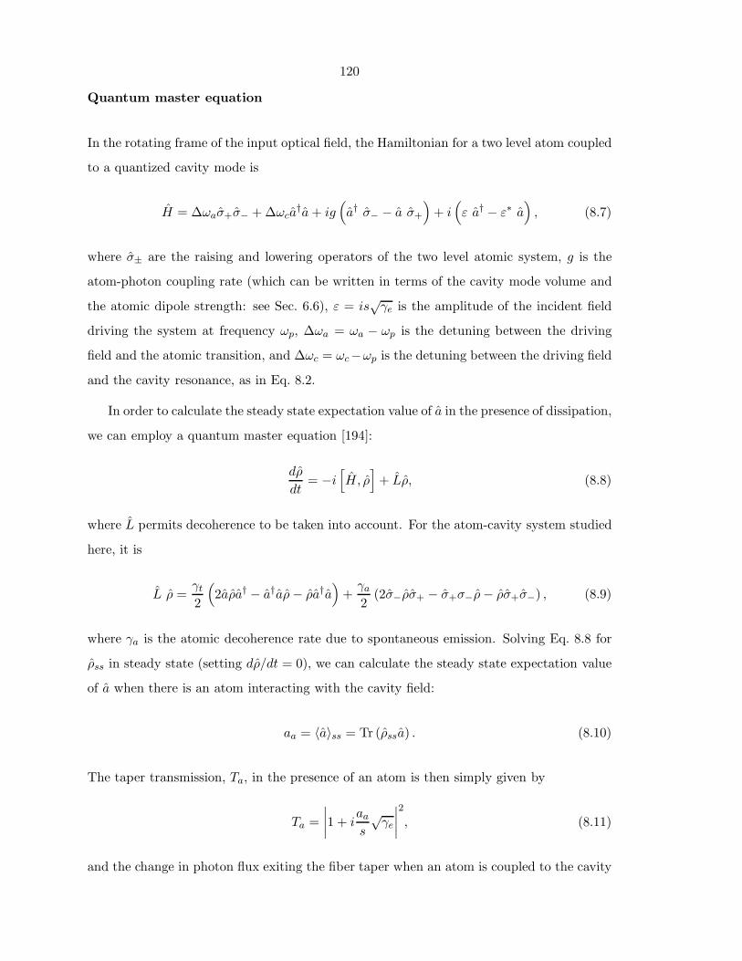
120
Quantum master equation
In the rotating frame of the input optical field, the Hamiltonian for a two level atom coupled
to a quantized cavity mode is
H = Δωaσ+σ− + Δωca†a+ ig
(a† σ− − a σ+
)+ i(ε a† − ε∗ a
), (8.7)
where σ± are the raising and lowering operators of the two level atomic system, g is the
atom-photon coupling rate (which can be written in terms of the cavity mode volume and
the atomic dipole strength: see Sec. 6.6), ε = is√γe is the amplitude of the incident field
driving the system at frequency ωp, Δωa = ωa − ωp is the detuning between the driving
field and the atomic transition, and Δωc = ωc−ωp is the detuning between the driving field
and the cavity resonance, as in Eq. 8.2.
In order to calculate the steady state expectation value of a in the presence of dissipation,
we can employ a quantum master equation [194]:
dρ
dt= −i
[H, ρ
]+ Lρ, (8.8)
where L permits decoherence to be taken into account. For the atom-cavity system studied
here, it is
L ρ =γt
2
(2aρa† − a†aρ− ρa†a
)+γa
2(2σ−ρσ+ − σ+σ−ρ− ρσ+σ−) , (8.9)
where γa is the atomic decoherence rate due to spontaneous emission. Solving Eq. 8.8 for
ρss in steady state (setting dρ/dt = 0), we can calculate the steady state expectation value
of a when there is an atom interacting with the cavity field:
aa = 〈a〉ss = Tr (ρssa) . (8.10)
The taper transmission, Ta, in the presence of an atom is then simply given by
Ta =∣∣∣∣1 + i
aa
s
√γe
∣∣∣∣2
, (8.11)
and the change in photon flux exiting the fiber taper when an atom is coupled to the cavity
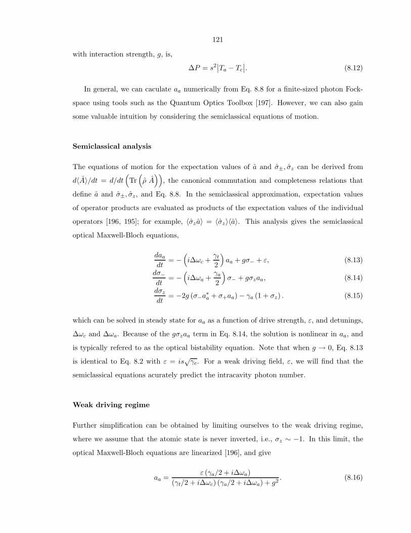
121
with interaction strength, g, is,
ΔP = s2∣∣Ta − Tc
∣∣. (8.12)
In general, we can caculate aa numerically from Eq. 8.8 for a finite-sized photon Fock-
space using tools such as the Quantum Optics Toolbox [197]. However, we can also gain
some valuable intuition by considering the semiclassical equations of motion.
Semiclassical analysis
The equations of motion for the expectation values of a and σ±, σz can be derived from
d〈A〉/dt = d/dt(Tr(ρ A))
, the canonical commutation and completeness relations that
define a and σ±, σz, and Eq. 8.8. In the semiclassical approximation, expectation values
of operator products are evaluated as products of the expectation values of the individual
operators [196, 195]; for example, 〈σza〉 = 〈σz〉〈a〉. This analysis gives the semiclassical
optical Maxwell-Bloch equations,
daa
dt= −
(iΔωc +
γt
2
)aa + gσ− + ε, (8.13)
dσ−dt
= −(iΔωa +
γa
2
)σ− + gσzaa, (8.14)
dσz
dt= −2g (σ−a∗a + σ+aa) − γa (1 + σz) . (8.15)
which can be solved in steady state for aa as a function of drive strength, ε, and detunings,
Δωc and Δωa. Because of the gσzaa term in Eq. 8.14, the solution is nonlinear in aa, and
is typically refered to as the optical bistability equation. Note that when g → 0, Eq. 8.13
is identical to Eq. 8.2 with ε = is√γe. For a weak driving field, ε, we will find that the
semiclassical equations acurately predict the intracavity photon number.
Weak driving regime
Further simplification can be obtained by limiting ourselves to the weak driving regime,
where we assume that the atomic state is never inverted, i.e., σz ∼ −1. In this limit, the
optical Maxwell-Bloch equations are linearized [196], and give
aa =ε (γa/2 + iΔωa)
(γt/2 + iΔωc) (γa/2 + iΔωa) + g2. (8.16)

122
Equation 8.16 can be used to illustrate the effect of the atom on the fiber coupled cavity
response. Note that in the limit that g → 0, aa → ac given by Eq. 8.3, as expected.
To illustrate the effect of the atom on the cavity response, consider the special case
where the cavity, atom, and driving field are all on resonance: Δωc = Δωa = 0. In this
case,
aa,o =2ε
γt + 4g2/γa=
2is√γe
γt + 4g2/γa, (8.17)
and
Ta,o =∣∣∣∣1 − 2γe/γt
1 + 4g2/γtγa
∣∣∣∣2
. (8.18)
In the limit that 4g2/γt � γa,
Ta,o →∣∣∣∣1 − 2γe
4g2/γa
∣∣∣∣2
∼ 1, (8.19)
and the relative change in the waveguide transmission due to the atom is
Ta,o
Tc,o∼(
1 +K
1 −K
)2
(8.20)
which can be abritrarily large as K → 1.
We can also predict what the maximum absolute change in waveguide output power
induced by the atom. From the Maxwell-Bloch equations, it can be shown that
1 + σz ∼ 2s2γe
g2, for 4g2/γt � γa, (8.21)
so that the weak driving condition σz ∼ −1 is satisfed when
s2 � Ps = s2s =g2
2γe=
1K
g2
2γi, for 4g2/γt � γa. (8.22)
where we call Ps the saturation input power. Subsituting Eqs. 8.19 and 8.6 into Eq. 8.12,
the change in the power exiting the waveguide when an atom is coupled to the cavity is
approximately given by
ΔPo = s2
∣∣∣∣∣1 −(
1 −K
1 +K
)2∣∣∣∣∣ , for 4g2/γt � γa, s� ss (8.23)

123
which is simply the power dropped into the empty cavity from the waveguide. From Eq.
8.22, the maximum atom induced change in power is
ΔPo � 2g2
γi
1(1 +K)2
. for 4g2/γt � γa (8.24)
It is also convenient to write this in terms of the maximum on-resonance empty cavity
intracavity photon number, ns, at which the weak driving approximation is valid:
ΔPo � γi ns, for 4g2/γt � γa (8.25)
where ns = 2g2/γ2t .
From Eq. 8.24, we can clearly see that the maximum atom induced change in power
increases as the intrinsic loss rate (γi) and the mode volume (∝ g−1/2) of the cavity decrease.
Another important observation is that the above analysis does not require the atom-cavity
system to be in the strong coupling regime. Rather, it is sufficient for the system to be in the
“bad-cavity” regime for single atom detection. Finally, recall that the example considered
above is on resonance (Δωc = Δωa = 0), and that full quantum simulations are required to
predict the cavity response for larger drive fields. Later in this section, we will examine the
dependence of Ta on detuning for cavities in both the strong and weak coupling regimes,
using both the semiclassical solution and fully quantum simulations.
8.1.2 Whispering gallery mode cavity
The presence of a degenerate or nearly denegerate mode significantly affects the cavity
response to an atomic dipole [198]. Even when the cavity modes are exactly orthogonal, if
the atom interacts with each mode, the modes become coupled. In the case of whispering
gallery mode cavities such as microdisks, a dipole scatters light from a single travelling
wave mode into both the clockwise and counterclockwise travelling modes, in a manner
analogous to surface roughness induced modal coupling [16, 15, 136, 198]. In this section,
we will augment the analysis given above to include a second cavity mode.
Assume that the cavity supports two degenerate, counter-propagating, whispering gallery
modes whose fields have amplitude a and b. Here we label a and b as the ccw (counter-
clockwise) and cw (clockwise) propagating modes, respectively. Because of the necessity of

124
phase matching, the waveguide will only couple to the co-propagating mode, which we will
assume is a. As in the single mode case, the normalized transmission through the waveguide
is
T =∣∣∣∣1 + i
a
s
√γe
∣∣∣∣2
. (8.26)
Any photons scattered into the counter-propagating mode b will couple to the backward
propagating waveguide mode; the normalized reflected waveguide signal is
R =∣∣∣∣i bs√γe
∣∣∣∣2
. (8.27)
In absence of coupling to an atom, the equations of motion for the empty cavity mode
amplitudes, ac(t) and bc(t), are
dac
dt= −
(γi
2+γe
2− iΔωc
)ac + iβbc + is
√γe, (8.28)
dbcdt
= −(γi
2+γe
2− iΔωc
)bc + iβ∗ac, (8.29)
where β is the coupling rate between modes intrinsic to the cavity (e.g., due to surface
scattering), and we have assumed that both modes have equal γi and γe.
In the limit that |β| � γt, we say that the cavity supports degenerate whispering gallery
modes. In this limit, ac and Tc are identical to those obtained for the single mode cavity.
However, as we will show below, when an atom interacts with a cavity in this limit, aa and
Ta are modified significantly relative to the single-mode result obtained above.
In the limit that |β| � γt, the cavity eigenmodes are most intuitively represented by
standing waves formed by even and odd supperpositions of the cw and ccw modes [16,
15, 136, 198]. These standing waves are uncoupled, and have resonant frequencies ωc ± β.
Because the standing waves have no azimuthal momentum, they radiate equally into both
the forward and backward waveguide modes, and the waveguide-cavity coupling is modified.
For ωp = ωc ± |β|, Tc,o can be calculated using the identical expression (Eq. 8.6) for the
single mode cavity, but with K → K ′ = γe/(γi + γe) = K/(K + 1).
The following analysis is valid for all values of β. However, we only consider limiting
on-resonance cases when β → 0, since in the |β| � γt limit, the single mode cavity results
with K → K ′ can be used.

125
Quantum master equation
The quantum master equation for a two-mode cavity is a simple generalization of the result
for the single mode cavity presented in Sec. 8.1.1 [198]. In the rotating frame of the input
optical field, the Hamiltonian for a two level atom coupled to the two quantized cavity
modes is
H = Δaσ+σ− + Δc
(a†a+ b†b
)+ ig
(a† σ− − a σ+
)+ (8.30)
ig(b† σ− − b σ+
)+ i(ε a† − ε∗ a
).
We have assumed that the atomic coupling strength, g, is equal for both modes of the cavity;
this is valid for degenerate whispering gallery modes that only differ in their direction of
propagation, but is not generally true.
For the degenerate whispering gallery mode cavity, L is given by
L ρ =γt
2
(2aρa† − a†aρ− ρa†a
)+γt
2
(2bρb† − b†bρ− ρb†b
)(8.31)
+γa
2(2σ−ρσ+ − σ+σ−ρ− ρσ+σ−) . (8.32)
After calculating the steady state master equation,ρss, from Eq. 8.8, the amplitudes of the
forward and backward propagating waveguide fields are:
aa = 〈a〉ss = Tr (ρssa) , (8.33)
ba = 〈b〉ss = Tr(ρssb). (8.34)
As in the single-mode case, aa and ba can be calculated numerically and substituted into
Eqs. 8.26 and 8.27 to determine R and T when an atom is coupled to the cavity.

126
Semiclassical analysis
The semiclassical equations of motion for an atomic dipole coupled to a degenerate whis-
pering gallery mode cavity are [198]
daa
dt= −
(iΔωc +
γt
2
)aa + iβ ba + gσ− + ε, (8.35)
dbadt
= −(iΔωc +
γt
2
)ba + iβ∗ aa + gσ− (8.36)
dσ−dt
= −(iΔωa +
γa
2
)σ− + gσz(aa + ba), (8.37)
dσz
dt= −2g (σ−(a∗a + b∗a) + σ+(aa + ba)) − γa (1 + σz) . (8.38)
Note that these equations do not reduce to the equations of motion for an atom coupled
to a single mode cavity when |β| = 0, except in the limit that g = 0, i.e., when the cavity
modes do not interact with the atom.
Weak driving regime
In the weak driving regime, where 〈σz〉 = −1 for all time, the semiclassical equations of
motion can be solved for aa and ba,
aa =ε(θc + g2/θa)
θc(θc + g2/θa) + g2/θc (iβ + iβ∗) + g2θc/θa + |β|2 , (8.39)
ba = aaiβ∗ − g2/θc
θc + g2/θa, (8.40)
where θc = iΔωc + γt/2, and θa = iΔωa + γa/2.
We can make further simplifications in the special case that |β| = 0, where Eq. 8.39
simplifies to:
aa =ε(θa + g2/θt)θaθt + 2g2
. for |β| = 0 (8.41)
Comparing this expression with the analogous expression (Eq. 8.16) for the single mode
cavity, we see that they are only equal in the limit that g → 0. If the atom and cavity are
on resonance with the drive field (Δωa = Δωc = 0), Eq. 8.41 reduces to
aa,o =2εγt
4g2/γtγa + 18g2/γtγa + 1
, for |β| = 0 (8.42)

127
and in the limit (g2 � γtγa),
aa,o =ε
γt=is√γe
γt. for 4g2/γt � γa, |β| = 0 (8.43)
The corresponding waveguide transmission is
Ta,o =(
1 − γe
γt
)2
=1
(1 +K)2. for 4g2/γt � γa, |β| = 0 (8.44)
For no-zero waveguide-cavity coupling (K > 0), Ta,o for the degenerate whipering gallery
mode cavity is clearly less than the unity transmission that was calculated in the single mode
case (Eq. 8.19). The maximum relative change in the waveguide transmission induced by
the atom isTa,o
Tc,o∼ 1
(1 −K)2, for 4g2/γt � γa, |β| = 0 (8.45)
and the change in waveguide output power is
ΔP = s2K(2 −K)(1 +K)2
. for 4g2/γt � γa, |β| = 0 (8.46)
Note that as K → 1, ΔP → s2/4.
From the optical Bloch equations, the input power below which σz ∼ −1 in the degen-
erate whispering gallery mode cavity is
s2 � Ps = s2s =2g2
γe, for 4g2/γt � γa, |β| = 0 (8.47)
and the maximum absolute change in waveguide output power induced by the atom is
ΔPo � 2g2
γi
|2 −K|(K + 1)2
= γi ns|2 −K|
4, for |β| = 0 (8.48)
where ns = 8g2/γ2t for the degenerate whispering gallery mode cavity. Note that for K = 1,
this is the same result as in the single mode cavity case, i.e., Eqs. 8.48 and 8.24 are equivalent.
Although the atom induces a smaller change in cavity transmission in degenerate whispering
gallery mode cavities than in single mode cavities, the saturation input power is higher, so
that the maximum atom induced change in output power is equal for both cases.
As with the single mode cavity analysis, from Eq. 8.48, we can clearly see that the

128
maximum atom induced change in power increases as the intrinsic loss rate (γi) and the
mode volume (∝ g−1/2) of the cavity decrease. Again, to observe single atom effects, the
above analysis does not require that the atom-cavity system be in the strong coupling
regime, but only in the “bad-cavity” regime.
Finally, recall that the above analysis assumes |β| = 0. In the limit that |β| �{g, γt,Δωc,Δωa}, it is more intuitive to analyze the cavity in the renormalized standing
wave basis, with detunings measured relative to the “new” modes. As discussed above,
in this case one finds that the atom-cavity system dynamics are similar to those of the
single-mode cavity presented in Sec. 8.1.1, with a modification to the coupling parameter
K to account for coupling between the standing wave modes and the backward propagating
waveguide modes.
8.1.3 Simulations
In this section, we simulate the effect of an atom on the waveguide coupled cavity response
for varying system parameters, by both numerically solving the quantum master equation,
and using the analytic expressions obtained from the semiclassical equations of motion in
Secs. 8.1.1 and 8.1.2. We find that at low powers is it sufficient to rely upon the semiclassical,
weak driving solution; but for powers approaching Ps = s2s, it is necessary to solve the fully
quantized quantum master equation. First we consider the behavior of a single mode cavity,
before studying a degenerate whispering gallery mode cavity.
Single mode cavity
Figure 8.2 compares the transmission, Tc, through a waveguide coupled to a bare cavity with
Q = {104, 105, 106} (γt/2π = {0.35, 3.5, 35} GHz), with the transmission Ta when an atom
is coupled to the same cavity. For these simulations, g/2π = 1 GHz and γa/2π = 0.005 GHz,
representing a Cs atom coupled to a cavity similar to the ∼ 9 μm diameter SiNx microdisk
studied in Ch. 6. As expected from the analysis in Sec. 8.1.1, at Δωc = 0, an atom induced
change in the waveguide transmssion is observed for input power Pi less than Ps. As the
input power increases above s2s, the change in transmission, |Ta −Tc|, decreases. It is useful
to note that when Pi � Ps, the semiclassical, weak driving regime solution given by Eq. 8.16
gives essentially indentical results to those obtained from a numerical solution of the density
matrix for the fully quantized systems (Eq. 8.8). For varying Q, the spectra of Ta(Δωc)
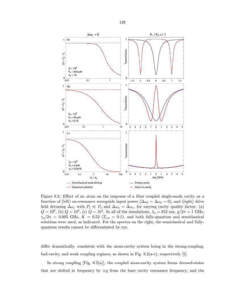
129
5 4 3 2 1 0 1 2 3 4 5
Tran
smis
sio
n
-1.5 -1 -0.5 0 0.5 1 1.5
0
1
Tran
smis
sio
n0
1
Tran
smis
sio
n
0
1
5 4 3 2 1 0 1 2 3 4 5
10.10.01
ΔT =
Ta
- Tc
0
1
10.10.01 10
10.10.01 10 100
ΔT =
Ta
- Tc
0
1
ΔT =
Ta
- Tc
0
1
Pi / Ps
Semiclassical weak driving
Quantum solution
Empty cavity
Atom in cavity
Δωc [GHz]
(a)
(b)
(c)
Q = 105
Ps = 90 pWns = 0.16
Q = 104
Ps = 9 pWns = 0.0016
Q = 106
Ps = 900 pWns = 16
Δωc = 0 Pi / Ps << 1
Figure 8.2: Effect of an atom on the response of a fiber coupled single-mode cavity as afunction of (left) on-resonance waveguide input power (Δωc = Δωa = 0), and (right) drivefield detuning Δωc with Pi � Ps and Δωa = Δωc, for varying cavity quality factor: (a)Q = 106, (b) Q = 105, (c) Q = 104. In all of the simulations, λo = 852 nm, g/2π = 1 GHz,γa/2π = 0.005 GHz, K = 0.52 (Te,o = 0.1), and both fully-quantum and semiclassicalsolutions were used, as indicated. For the spectra on the right, the semiclassical and fully-quantum results cannot be differentiated by eye.
differ dramatically, consistent with the atom-cavity system being in the strong-coupling,
bad-cavity, and weak coupling regimes, as shown in Fig. 8.2(a-c), respectively [5].
In strong coupling [Fig. 8.2(a)], the coupled atom-cavity system forms dressed-states
that are shifted in frequency by ±g from the bare cavity resonance frequency, and the

130
waveguide transmission spectrum is dramatically modified. As γt increases [Fig. 8.2(b-c)],
the dressed states no longer form spectrally distinct features in the waveguide transmission.
However, on-resonance, the waveguide transmission continues to be affected by the atom,
due to coherent reflection by the atomic dipole. The resulting electromagnetic induced
transparancy-like feature persists even for very large γt. Using the semiclassical analysis
from Sec. 8.1.1, it can be verified that the spectral width of this feature is approximately
Δω ∼ γa + g2/γt, i.e., the Purcell enhanced spontaneous emission rate.
Degenerate whispering gallery mode cavity
As discussed in Sec. 8.1.2, the cavity response is significantly modified by coupling between
degenerate counter-propagating cavity modes, mediated by the atomic dipole as well as by
cavity imperfections. Figure 8.3 compares the waveguide transmission past a degenerate
whispering gallery mode cavity with no intrinsic mode-coupling (|β| = 0), with and without
an atom, for the same parameters as in Fig. 8.2.
The atom-cavity spectrum is most dramatically modified by the coupling from the atom
into both the cw and the ccw cavity modes when the system is in strong coupling. As
shown in Fig. 8.3(a), three resonant dips in the transmission are predicted. Notably, the
resonant frequencies of the outer dips are split by ±√2g relative to the center dip. The
factor of√
2 is due to the standing wave nature of the coupled cw and ccw modes, and the
resulting enhancement of the maximum field strength. From an atom detection perspective,
note that the maximum atom induced change in transmission, ΔT , is smaller than in the
single mode cavity case. Also, note that a non-zero reflected signal is generated, which
potentially can be used for atom detection. The power dependence and onset of saturation
of ΔT is consistent with predictions from Sec. 8.1.2. Note that because of the large Fock
space associated with simulating two cavity modes at large drive strengths, the less memory
intensive stochastic Schrodinger equation (SSE) technique [199, 200, 201, 197] was employed
to calculate ΔT (Pi).
In the bad cavity limit, shown in Figs. 8.3(b,c), the effect of the degenerate cavity mode
on the atom-cavity spectrum is less dramatic: The spectra has a similar shape as in the single
mode case [Fig. 8.2(b)], with a notch in the transmission centered at Δωc = 0. However,
as in the strong coupling case, Ta,o does not reach unity, and the maximum atom induced
change in transmission is smaller than in the single mode cavity. Again, the reflected signal

131
5 4 3 2 1 0 1 2 3 4 5
-1.5 -1 -0.5 0 0.5 1 1.5
0
1
0
1
0
1
5 4 3 2 1 0 1 2 3 4 5
10.10.01
ΔT =
Ta
- Tc
0
1
10.10.01 10
10.10.01 10 100
ΔT =
Ta
- Tc
0
1
ΔT =
Ta
- Tc
0
1
Q = 105
Ps = 360 pWns = 0.6
Pi / Ps
Semiclassical weak driving
Quantum solution (SSE)
Empty cavity
Atom in cavity
Δωc [GHz]
(a)
(b)
(c)
Q = 104
Ps = 36 pWns = 0.006
Q = 106
Ps = 3.6 nWns = 60
R
T
R
T
R
T
Δωc = 0 Pi / Ps << 1
Figure 8.3: Same simulations as in Fig. 8.3, but including a degenerate whispering gallerymode (|β| = 0). Also shown is the reflected waveguide signal. Both fully-quantum andsemiclassical solutions were used, as indicated. For the spectra on the right, the semiclas-sical and fully-quantum results can not be differentiated by eye. The power dependentcalculations in (a) were limited to Pi < Ps for computational reasons.
is non-zero.
Standing wave whispering gallery mode cavity
Fig. 8.4 shows typical waveguide-coupled cavity response spectra when β = 9 GHz, and
the atomic dipole is on resonance with the standing wave cavity mode at ωo − β. In the

132
-5 0 5 10 15 20 250
1
0
1
Empty cavity
Atom in cavity
Δωa [GHz]
R
T
-5 0 5 10 15 20 25
R
T
2β 2β
Δωa [GHz]
(a) (b)
Figure 8.4: Same simulations as in Fig. 8.3, but with microcavity induced coupling betweenthe degenerate whispering gallery modes (|β|/2π = 9 [GHz], β real). The atomic dipoleis detuned by −|β| from the uncoupled cavity resonance frequency, so that is spectrallyaligned with the lower frequency standing wave mode. Although γe is unchanged from thesimulation results in Figs. 8.3 and 8.2, in the standing wave basis K → K ′ = K/(K + 1) =0.34. Also shown is the reflected waveguide signal. The semiclassical and fully-quantumresults cannot be differentiated by eye.
presence of an atom, the cavity mode responds nearly identically to the single-mode cavities
studied in Sec. 8.1.1, in both the strong- and bad-cavity regimes (Fig. 8.4(a,b), respectively).
Notably, the on-resonance transmission when an atom enters the cavity, Ta,o, recovers to
unity. The principle differences are that g → √2g, due to the standing wave nature of
the modes, and that for a given γe and γi, Tc,o is larger, as expected from the discussion
above. Additionally, the reflected waveguide signal is non-zero for the empty cavity, as the
standing wave mode radiates into both the forward and backward propagating waveguide
modes. The power dependence is not shown, but is similar to the single mode case, but
with Ps renormalized to take into account the modified waveguide coupling.
8.2 Single atom detection: signal to noise
In the preceding section, we showed that a single atom interacting with the field of a
microcavity can significantly alter the cavity response, so that in principle the presence of
an atom can be detected as it transits the cavity field. However, to determine whether single

133
atom transits are observable in the laboratory, the photon detection bandwidth and noise
floor must be taken into account. In this section, we consider practical photon detection
schemes, including single photon counting (SPC), avalanche photodiode (APD) detection,
and heterodyne (HD) detection, using specifications for commercially available detectors.
We quantitatively evaluate their suitability for single atom detection by calculating the
maximum expected signal to noise obtainable with them, given the expected atom-induced
change in cavity response and saturation cavity input power calculated in the previous
section.
8.2.1 Signal to noise ratio
The signal to noise ratio (SNR) for single atom detection using a fiber-coupled microcavity
can be defined in terms of the change in the observed waveguide output signal induced by
one or more atoms interacting with the cavity relative to the amplitude of the noise on the
output signal when there are no atoms interacting with the cavity. Writing Sc and Sa as the
measured signal (e.g., voltage or number of photons) when there are no atoms and when
one or more atoms are interacting with the cavity, respectively, a suitable definition for the
SNR is
SNR =ΔSσS
=|Sa − Sc|
σS, (8.49)
σS =√σ2
t + σ2sn (8.50)
where σt and σsn are the standard deviations of S due to technical noise and shot noise
(SN), respectively. Note that this SNR is defined in terms of optical power, and not elec-
tronic power. Technical noise is independent of S, and is determined by the detector and
the operating bandwidth. Shot noise depends on the output signal, and one can present
arguments for whether the shot noise on Sc (during the atom transit) or Sa (when the cavity
is not interacting with an atom) should be considered. As in Ref. [173], here we take
σsn =√σ2
sn,a + σ2sn,c, (8.51)
where σsn,a and σsn,c are the shot noise on Sa and Sc, respectively. This definition provides
an accurate measure of the fidelity with which atom-cavity dynamics can be observed. An

134
alternate definition, in which σsn = σsn,c, provides an exagerated measure of whether a
change in signal can be prescribed to an atom transit, but does not take into account the
possiblity of missing a transit due to shot noise fluctuations in the atom-induced signal.
Bandwidth requirements
In general, both the noise and signal amplitudes depend upon the detection bandwidth,
Δν. For the experiment considered here, Δν is determined by the time that an atom
spends within the near field of the cavity. Atoms that are laser cooled such that they travel
with mean thermal velocities of ∼ 2.5 cm/s [180] will transit the 250 nm thickness of a
typical microdisk or photonic crystal microcavity in 10 μs [173]. This requires a detection
bandwidth of Δν = 0.1 − 1 MHz, corresponding to integration times of τ = 1/2Δν ∼0.5 − 5 μs.
Photon collection efficiency
Using the waveguide-cavity coupling formalism presented above, imperfect cavity-waveguide
coupling efficiency due to intrinsic cavity loss (“bad-loss”) is taken into account by the cou-
pling parameter K. However, broadband “insertion-loss” associated with scattering, radia-
tion, or absorption within the waveguide needs to be taken into account. This insertion loss
can be lumped together, and the transmission between the waveguide-microcavity coupling
region and the photon detection apparatus can be simply expressed as ηw. In practice,
ηw ∼ 0.5-0.8 is typical for a fiber taper permanently coupled to a microdisk and installed
in the atom cooling vacuum chamber, as described in Ch. 7.
Idealized SNR
In a perfect photodetector, there is no technical noise, so that the SNR is only limited by the
quantum fluctuations in the detected signal (shot noise), the transmission of the waveguide
(ηw), and the quantum efficiency of the detector (ηd). Generally, the measured signal is the
change in the measured number of photon counts per time bin when an atom interacts with
the cavity (Na) compared to when there is no atom interacting with the cavity (Nc). For
a given integration time τ , S and σS are expressed in terms of the waveguide powers, Pa
and Pc (in units of photons per unit time), transmitted past the waveguide-cavity coupling

135
region:
S = τηwηd|Pa − Pc| = τηwηdΔP, (8.52)
σS =√τηwηd(Pa + Pc). (8.53)
The SNR is then simply given by
SNR∣∣SN
=ΔP√Pa + Pc
√ηwηdτ =
ΔN√Na +Nc
√ηwηd, (8.54)
where ΔN = |Na −Nc|. For on-resonance detection, in the case that Pc = 0 (K → 1), Eq.
(8.54) reduces to
SNR∣∣SN
=√
ΔN√ηwηd. (8.55)
In practice, technical noise will always be present. Next, we discuss the limitations of
practical photodetection schemes.
8.2.2 Photon detection schemes
Below we briefly review the noise properties of photodetection schemes in the context of
single atom detection experiments.
Single photon counting
Commerically available single photon counting modules (SPCM) offer essentially shot noise
limited detection “out of the box” for very low light levels. With dark count rate of less than
25 photons per second (Perkin Elmer SPCM-AQP-16), SPCMs have almost no electronic
noise on the time scales over which atom transits are expected to occur. Their primary
limitation from an atom detection point of view is their large dead time between successive
photon counting events, which typically limits the maximum photon flux that they can
measure to ∼ 107 photons per second. Assuming that {ηwPc, ηwPa} ≤ PSPCM, where PSPCM
is the saturation power of the SPCM, the SNR is simply given by Eq. 8.54. However, for
{ηwPc, ηwPa} > PSPCM, the saturation power limits the SNR:
SNR∣∣SPCM
< PSPCM ×√
ηdτ
Pc + Pa. (8.56)

136
If PSPCM = 107 photons/second and Pc = 0, for a τ = 1 μs integration time,
SNR∣∣SPCM
<√
10 ηd. (8.57)
APD detection
Avalanche photodiodes (APD) can provide high-bandwidth, low noise photodetection at
low light levels. As with SPCMs, they are fabricated using reverse biased photodiodes, and
rely upon avalanche multiplication of photo-generated electrons to provide gain without
adding significant electronic noise. Unlike SPCMs, they are not reverse biased past their
breakdown point, and can operate at higher powers and bandwidths.
For a given atom-induced change in optical power ΔP (photons per unit time), the
signal measured using an APD-amplifier module is
S = R ηwΔP, (8.58)
where R = Ro�ω, and Ro is the lumped responsivity of the APD detector module (i.e., APD
quantum efficiency, APD gain, and electronic amplifier transimpedance), usually expressed
in units of V/W. The noise has contributions from both the APD (shot noise) and the
amplifier electronics, and is written as σAPD and σt, respectively. The total noise is:
σSc =√σ2
APD + σ2t . (8.59)
The amplifier noise is typically quoted as a spectral density, w, in units of W/√
Hz, so that
σt = R w√
Δν = Rw√2τ, (8.60)
where w = w/�ω. The APD noise,
σAPD = R√FPsn, (8.61)
is fundamental, as it is proportional to the photon shot noise power [3]:
Psn =
√ηw(Pc + Pa)
ηdτ. (8.62)

137
The F term is the “noise factor” characteristic of any stochastic avalanche amplification
process [202]; generally F ≥ 1. Combining the above expressions, the APD SNR for atom
detection is
SNR∣∣APD
=ΔP ηw√
F (Pc + Pa)ηw/ηdτ + w2/2τ. (8.63)
In the limit that electronic noise is small compared to shot noise, Eq. 8.63 becomes
SNR∣∣APD
=ΔP√Pa + Pc
√τηwηd
F, for ηw(Pa + Pc) � w2ηd/2F (8.64)
which is the “ideal” shot noise limited result, Eq. 8.54, scaled by F−1/2.
Heterodyne detection
Ideally, optical heterodyne detection [3, 203] can reach the shot noise limit at high band-
widths, even using photodetectors with large σt compared to the the signal of interest.
Heterodyne detection measures the amplitude of a beat note formed by two spatially over-
lapping but frequency detuned optical beams incident on a photodetector. Given a signal
with optical power, Ps (photons per unit time), the heterodyne signal is,
S = R 2ηh
√PsPlo, (8.65)
where R is the responsivity of the detector being used, and Plo is the power of a frequency
detuned local oscillator (LO) that is spatially overlapped with the Ps beam, and ηh is the
heterodyne efficiency. In practice, ηh depends on the mode matching of the LO and the
signal beams, and the mix-down electronics that filter for the beat note. If the LO is not
phase locked relative to the signal, ηh ≤ 0.5.
For Plo � Ps, the noise of the heterodyne signal is given by
σSc =√σ2
h + σ2lo, (8.66)
where σh is the technical electronic heterodyne noise, and σlo is the LO shot noise. Ideally,
the electronic noise is determined by the measurement bandwidth and the noise power

138
spectral density, w, of the detector at the frequency of the beat note, νh:
σh = R w(νh)√
Δν. (8.67)
The LO shot is given by,
σlo = R
√Plo
ηdτ, (8.68)
and the heterodyne SNR for atom detection is,
SNR∣∣HD
=2ηh|
√ηwPaPlo −
√ηwPcPlo|√
Plo/ηdτ + w2/2τ. (8.69)
In the limit that Plo � ηdw2/2, usually achieved by increasing Plo,
SNR∣∣HD
= 2ηh|√Pa −
√Pc|√ηwηdτ . for Plo � ηdw
2/2 (8.70)
If Pc ∼ 0, this is simply
SNR∣∣HD
= 2ηh
√Pa
√ηwηdτ , (8.71)
= 2ηh
√ΔN
√ηwηd, (8.72)
where ΔN is the atom induced change in photon counts per time bin, τ . Again, this
corresponds to the “ideal” shot noise limited SNR, Eq. 8.54, scaled by 2ηh.
8.2.3 Simulations
Using the expressions for SNR for the detectors described in Sec. 8.2.2, as well as the power-
dependent atom-cavity response calculations from Sec. 8.1.3, we now calculate the SNR for
realistic single atom detection, for varying cavity parameters and drive strength. Table 8.1
lists the detector parameters used in the calculations in this section. All of these parameters
correspond to commercially available components, as listed in the table.
Figure 8.5 shows calculated atom-detection SNR for a single mode microcavity and a
degenerate whispering gallery mode microcavity, assuming on-resonance detection, atom-
photon interaction rate, g/2π = 1 GHz, and a τ = 3 μs integration time, for Q = ω/γt =
[106, 105, 104], as in Sec. 8.1.3. As discussed in Ch. 6, [g/2π,Q] = [1 GHz, 106] should be

139
achievable for a Cs atom interacting with a silicon nitride microdisk cavity [17]. In addition
to considering APD, SPCM, and HD detection, the “ideal” shot noise limited SNR (for ηw
and ηd given in Table 8.1) is shown as function of waveguide input power. Each of the
detection schemes has an optimal input power at which the SNR is maximized. In the case
of the SPCM, the SNR is maximized when the waveguide output power is ∼ PSPCM/ηd
as expected from Eq. 8.57. So long as ηdηwPs > PSPCM is satisfied, the maximum SPCM
SNR is largely unaffected by g and γt. For the other detectors, with saturation powers far
above ηdηwPs, Ps is a very good prognosticator of the input power at which the SNR is
maximized. The maximum SNR obtainable with the degenerate whispering gallery mode
cavity is essentially equal to that in the corresponding single mode cavity, albeit at a
higher input power (recall that Ps|2-mode = 4Ps|1-mode), confirming our intuition from Sec.
8.1.2. The smaller change in cavity response characteristic of the degenerate cavity is
only deterimental for the SNR for SPCM detection, where ΔP is limited by the detector
saturation.
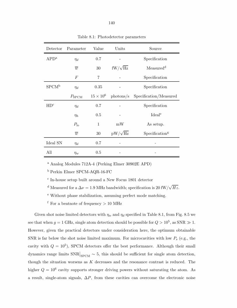
140
Table 8.1: Photodetector parameters
Detector Parameter Value Units Source
APDa ηd 0.7 - Specification
w 30 fW/√
Hz Measuredd
F 7 - Specification
SPCMb ηd 0.35 - Specification
PSPCM 15 × 106 photons/s Specification/Measured
HDc ηd 0.7 - Specification
ηh 0.5 - Ideale
Plo 1 mW As setup.
w 30 pW/√
Hz Specificationg
Ideal SN ηd 0.7 - -
All ηw 0.5 - -
a Analog Modules 712A-4 (Perking Elmer 30902E APD)b Perkin Elmer SPCM-AQR-16-FCc In-house setup built around a New Focus 1801 detectord Measured for a Δν = 1.9 MHz bandwidth; specification is 20 fW/
√Hz.
e Without phase stabilization, assuming perfect mode matching.f For a beatnote of frequency > 10 MHz
Given shot noise limited detectors with ηw and ηd specified in Table 8.1, from Fig. 8.5 we
see that when g = 1 GHz, single atom detection should be possible for Q > 105, as SNR � 1.
However, given the practical detectors under consideration here, the optimum obtainable
SNR is far below the shot noise limited maximum. For microcavities with low Ps (e.g., the
cavity with Q = 105), SPCM detectors offer the best performance. Although their small
dynamics range limits SNR∣∣SPCM
∼ 5, this should be sufficient for single atom detection,
though the situation worsens as K decreases and the resonance contrast is reduced. The
higher Q = 106 cavity supports stronger driving powers without saturating the atom. As
a result, single-atom signals, ΔP , from these cavities can overcome the electronic noise

141
0
1
2
3
4
SNR
5
10
15
20
25
30
0
2
4
6
8
10
APDHDSPCMIdeal SN
10.10.01
10.10.01 10
10.10.01 10 100
Pi / Ps
0
SNR
SNR
Q = 105
Ps = 90 pWns = 0.16
Q = 104
Ps = 9 pWns = 0.0016
Q = 106
Ps = 900 pWns = 16
0
1
2
3
4
10.10.01 10 100
Pi / Ps
0
2
4
6
8
10
10.10.01 10
Q = 105
Ps = 360 pWns = 0.6
Q = 104
Ps = 36 pWns = 0.006
Q = 106
Ps = 3.6 nWns = 60
Single mode cavity Degenerate whispering gallery mode cavity
10.10.01
(a)
(b)
(c)
0
5
10
15
20
25
30
35
Figure 8.5: Calculated SNR for a fiber coupled single mode (left) and degenerate whisperinggallery mode (right) microcavity with g/2π = 1 GHz and (a) Q = 106, (b) Q = 105, (c)Q = 104. In all of the calculations, λo = 852 nm, γa/2π = 0.005 GHz, Δωa = Δωc = 0,K = 0.52 (Te,o = 0.1). The various detector parameters are given in Table 8.1. The powerdependent calculation in (a) was limited to Pi < Ps for computational reasons.
of the APD and HD detectors and provide improved performance: SNR > 10 should be
achievable.
Alternately, since Ps = s2s scales with g2/γt (∝ Q/V ), the SNR can be improved by using
a smaller mode volume cavity, so long as Q does not degrade too quickly as the mode volume
shrinks. Figure 8.6 shows calculated SNR for a microcavity with g/2π = 10 GHz, and

142
5
10
15
20
25
30
APDHDSPCMIdeal SN
10.10.010
SNR
Q = 104
Ps = 900 pWns = 0.16
Q = 105
Ps = 9 nWns = 16
10.010.001
(a)
10 100
20
40
60
80
100
0
0.1
(b)
Pi / Ps Pi / Ps
Figure 8.6: Calculated SNR for fiber coupled single mode microcavities with g/2π = 10 GHzand (a) Q = 105, (b) Q = 104. In all of the calculations, λo = 852 nm, γa/2π = 0.005 GHz,Δωa = Δωc = 0, K = 0.52 (Te,o = 0.1). The various detector parameters are given in Table8.1.
Q = [104, 105]. These parameters should be achievable using a high quality photonic crystal
nanocavity [11, 12], such as that studied in Ch. 4, but fabricated from a material suitable
for near-visible wavelengths. As expected, when [g/2π,Q] = [10 GHz, 104] [Fig. 8.6(a)], the
microcavity performs similarily to the [g/2π,Q] = [1 GHz, 106] microcavity [Figure 8.5(a)].
Figure 8.6(b) shows the expected performance of a cavity with [g/2π,Q] = [10 GHz, 105].
Shot noise limited SNR ∼ 100 should be possible, and SNR > 30 is expected using direct
APD detection. This is a significant improvement over the higherQ, but larger mode volume
cavity, and promises high-quality single atom transit measurements. Beyond the benefit of
improved single-atom sensitivity, an advantage of pursuing the route of miniturization,
rather than working to further increase Q, is robustness. Mode volume is largely unaffected
by fabrication imperfections, and lower Q cavities are less sensitive to surface contamination
and spectral detuning.
8.3 Summary
In this section, we have shed light on the role of mode volume and quality factor on the
sensitivity of a microcavity to single atom transits. In particular, through analytic analysis
and verification with numerical simulations, we have shown that the relevant figure of merit
143
is g2/γt, which is proportional to Q/V . Using realistic detector noise parameters, we have
studied the expected performance of a range of microcavities, and determined that single
atom transits should be observable with the microdisk cavities studied in this thesis, but
that larger Q/V devices, and/or longer atom-cavity interaction times, are necessary for
high quality signals. It is expected that photonic crystal nanocavities will offer significantly
improved detection fidelity.

144
Appendix A
Bloch modes and coupled mode theory
A physical problem of practical interest is the coupling between Bloch modes in seperate
interacting electromagnetic waveguides. This problem arises when considering strongly
periodic waveguides, such as those formed by line defects in high refractive index contrast
photonic crystals [204, 52, 113, 58]. In these structures, it is not accurate to represent
the fields of the unperturbed waveguides using a plane wave basis; a Bloch mode basis
must be used. In this appendix an approximate coupled mode theory suitable for studying
coupling between strongly period waveguides is derived. Additionally, some mathematical
identities useful for working with and understanding the physical properties of Bloch modes
are presented.
A.1 Formulating Maxwell’s equations
In absence of free charge and current, and for fields with eiωt time dependance, Maxwell’s
equations are given by
∇ ·D = 0 (A.1)
∇ × H − iωD = 0 (A.2)
∇ × E + iωB = 0 (A.3)
∇ · B = 0, (A.4)

145
where, for non-magnetic material,
D(r) = ε(r)E(r) (A.5)
B(r) = H(r). (A.6)
It can be shown [69] that solutions to Maxwell’s equations corresponding to a structure
whose dielectric constant, ε(r), is periodic in z with lattice constant Λ,
ε(x, y, z + nΛ) = ε(x, y, z) (A.7)
n = 0,±1,±2, . . .
can be written in Bloch form
Ek(r) = e−ikzek(r), (A.8)
where
ek(x, y, z + nΛ) = ek(x, y, z), (A.9)
and a eiωt time dependance is assumed. Writing the field in Bloch form, taking the curl of
(A.3) and substituting (A.2), we get
∇ × ∇ × Ek =ω2
c2ε(r)Ek, (A.10)
or, more explicitly,
Hkek(r) =[−k2z × z×−ik(∇ × z × +z × ∇×) + ∇ × ∇×] ek(r) =
ω2
c2ε(r)ek(r).
(A.11)
Equation (A.10) is often solved as an eigenvalue problem for ω parameterized by the
wavenumber, k, giving a dispersion relation, ω = ω(k). In general (A.10) will have multiple
solutions for a given ω. Each of these solutions is a mode of the structure described by
ε(r) and can be labeled by a wavenumber, k = km. To be explicit, Ek can be labeled
as Ekm to distinguish between modes. For radiating modes, km will form a continuum,
while for bound modes, km will form a discrete set. It is important to note that for each
mode Ekm, by time reversal symmetry, there is a corresponding eigenfunction, E−km, with
eigenvalue ω(−km) = ω(km), which represents a mode propagating in the −z direction.

146
The relationship between the forward and backward propagating modes will be examined
in subsequent sections. Additionally, for each km′ = km + nG where the reciprocal lattice
vector G = 2πΛ and n is any integer, there corresponds a mode that is physically identical
to the mode labelled by km [69, 205]. As a result, in considering the space of eigenmodes,
it is sufficient to restrict k to the first Brillouin zone: |k| ≤ G2 .
A.1.1 Orthogonality of Bloch modes
Before deriving coupled mode equations, it is useful to derive an orthogonality relationship
between modes. In [68] it is shown that Hk is Hermitian, so that for fixed k and varying
eigenfrequencies, ωm, equation (A.11) gives
∫Vdr ε(r) e∗k(ωn)(r) · ek(ωm)(r) = δωn, ωm , k(ωn) = k(ωm) (A.12)
where the integration is over a single unit cell defined by V = {r | z0 ≤ z ≤ z0 + Λ}. In
coupling between modes in linear dielectrics, however, ω is typically fixed to ensure non-zero
time averaged power transfer between modes, while k varies between modes as described
above.
Another othorgonality relation can be derived using a reciprocity theorem similar to
that used in [72]. Define F as
F = Ekn × H∗km
+ E∗km
× Hkn , (A.13)
where Ek(n,m)and Hk(n,m)
are solutions to Maxwell’s equations (A.1-A.4) for some ε(n,m).
Using Maxwell’s equations and standard vector identities, the divegence of F is:
∇ ·F = −iωEkn · E∗km
[εn(r) − ε∗m(r)]. (A.14)
From (A.14), if εn = ε∗m, then ∇ · F = 0, and integrating over a unit cell:
∫V
∇ ·F dV =∫SF · dS (A.15)
=[ ∫
z=z0
−z +∫
z=z0+Λz]·F dx dy +
∫S∞
F · dS (A.16)
= 0,

147
where S is the surface bounding V, and S∞ represents the surface of V at ρ =√x2 + y2 →
∞. Since the area of S∞ ∝ ρΛ and |F| ∝ 1/ρ2 (at most for physical fields) on S∞, the
last term in (A.16) does not contribute. Recalling that Bloch modes are eigenvectors of the
translation operator:
TΛz(Ekm ,Hkm) = e−ikmΛ(Ekm,Hkm), (A.17)
equation (A.16) becomes
[1 − e−i(kn−km)Λ
] ∫z=z0
(Ekn × H∗
km+ E∗
km× Hkn
) · z dx dy = 0. (A.18)
By Bloch’s theorem, the Bragg condition,
kn − km =2πjΛ, j = ±1,±2... (A.19)
can only be satisfied by modes that are identical moduolo a reciprocal lattice vector label.
By restricting our eigmodes to the first Brillouin zone, Eq. (A.19) can never be satisfied,
requiring that if km = kn,
∫z
(Ekn ×H∗
km+ E∗
km× Hkn
) · z dx dy = 0, (A.20)
for Eq. (A.18) to hold. Equation (A.20) is a power orthogonality relationship that has the
advantage of not requiring integration in the propagation direction.
If km = kn, assuming there are no degeneracies, modes n and m are identical and the
“power” defined by the left hand side of (A.20) is non-zero; however, it can be shown that
it is independant of z. We have:
F = Ekm × H∗km
+ E∗km
× Hkm. (km = kn) (A.21)
Integrating ∇ ·F over a plane of constant z, and using (A.14) as well as the 2-D divergence
thereom (see [72])
∫z∇ · F dx dy =
∂
∂z
∫zF · z dx dy = 0 (A.22)

148
or
∂
∂z
∫z
(Ekm × H∗
km+ E∗
km× Hkm
) · z = 0. (A.23)
This is simply a statement of power conservation: For modes propagating in the z direction,
the power flux through any x-y plane is independent of z. Equations (A.20) and (A.23)
state that the eigenmodes of a periodic ε(r) can be normalized by their power, and that
they are power orthogonal. These relations will be critical in the developement of a coupled
mode theory below.
A.1.2 Additional properties of Bloch modes
Because of the lack of translational invariance in a periodic ε(r), the standard relationships
between forward and backward propagating modes derived in [72] do not hold for Bloch
modes. Fortunately, by considering the symmetries of the system, some useful relationships
can be derived.
First, consider time reversal symmetry. Since the operator defining E(r, t) obtained
from Maxwell’s equations is invariant under time reversal t → t′ = −t, the time reversed
E(r,−t) is also a solution. From this, one can show that [69]
E−k = E∗k (A.24)
H−k = −H∗k.
We can arrive at this result directly from the eigenvalue equation for ek without specifically
considering time-reversal. From (A.11), it is clear that H−k = H∗k, so that the eigenvalue
problem for e−k can be written as
H−k e−k =ω2
c2ε e−k (A.25)
H∗k e−k =
ω2
c2ε e−k (A.26)
Hk e∗−k =ω2
c2ε e∗−k (A.27)
for real ε. This implies that e∗−k is an eigenmode of Hk, but we know that the eigenmode

149
of Hk is given by ek, so that
e∗−k = ek (A.28)
or
e−k = e∗k (A.29)
which is the relationship we are want. Next consider the Bloch part of the magnetic field
which from Maxwell’s equations is related to he Bloch part of the electric field by
hk =1i ω
(−ikz + ∇) × ek = B k ek. (A.30)
Clearly B −k = −B∗k, so that
h−k = B −k e−k (A.31)
= −B∗k e∗k (A.32)
= − (B k ek)∗ (A.33)
= −h∗k (A.34)
which is again the desired relation.
Next consider spatial inversion symmetry. Unlike translationally invariant waveguides,
a periodic structure such as a photonic crystal waveguide only has inversion symmetry
about a finite number of high symmertry points, and in some cases may not have inversion
symmertry at all in the direction of propagation. If it does, i.e., if
ε(x, y,−z) = ε(x, y, z) (A.35)
for z = 0 defined at an appropriate high symmetry point of the structure, then (see [69])
[Oσz ,
1ε(r)
∇ × ∇×]
= 0 (A.36)

150
and, as a result,
1ε(r)
∇ × ∇ × (OσzEk) = Oσz
(1ε(r)
∇ × ∇ × Ek
)
=ω2
c2(OσzEk); (A.37)
i.e., OσzEk is an solution to the original eigenvalue problem (A.10). Next, it can be shown
that OσzEk is a Bloch mode:
TΛz(OσzEk) = Oσz(TσzΛz Ek)
= Oσz(e−ik(−Λ)Ek)
= Oσz(e−i(−k)ΛEk)
= e−i(−k)Λ(OσzEk) (A.38)
i.e., OσzEk is a Bloch state with wave number −k:
OσzEk = E−k. (A.39)
But we can also operate directly on the eigenvector with the inversion operator:
OσzEk(x, y, z) = σzEk(x, y,−z). (A.40)
These last two equations combine to give
E−k(x, y, z) = σz Ek(x, y,−z). (A.41)
Since the electric field E is a true vector [fundamentally defined by a vector (position) times
a scalar (charge)] [206], under inversion it transforms as
σz E · (x, y, z) = E · (x, y,−z) (A.42)

151
finally giving
E−k(x, y, z) · (x, y, z) = Ek(x, y,−z) · (x, y,−z) (A.43)
e−k(x, y, z) · (x, y, z) = ek(x, y,−z) · (x, y,−z).
A similar derivation can be followed with the magnetic field, with the only difference re-
sulting from the fact that H is a pseudovector [fundamentally defined as the cross product
of two vectors (postion and current density)] [206] so that under inversion
σz H · (x, y, z) = H · (−x,−y, z), (A.44)
giving
H−k(x, y, z) · (x, y, z) = Hk(x, y,−z) · (−x,−y, z) (A.45)
h−k(x, y, z) · (x, y, z) = hk(x, y,−z) · (−x,−y, z).
Since ek and hk are periodic functions of z, at the edges and center of the unit cell, zn =
±nΛ/2, we have ek(−zn),hk(−zn) = ek(zn),hk(zn) and
e−k(x, y, zn) · (x, y, z) = ek(x, y, zn) · (x, y,−z) (A.46)
h−k(x, y, zn) · (x, y, z) = hk(x, y, zn) · (−x,−y, z).
These are the same relations that hold for all z (as opposed to the set of zn, given here) in
translationally invariant waveguides [72]. Combining these relations with the time reversal
relations allows the phase of the components of the Bloch modes at these high symmetry
points to be fixed. From (A.46) and (A.29, A.31) at the high symmertry points, zn, we get
ek(x, y, zn) · (x, y, z) = e∗k(x, y, zn) · (x, y,−z) (A.47)
hk(x, y, zn) · (x, y, z) = h∗k(x, y, zn) · (x, y,−z)
i.e., the transverse parts are purely real and the longitudinal parts are purely imaginary at
zn. This property can be used to obtain a more compact orthogonality relationship at these

152
points:
∫zn
(e∗km× hkn) · z dx dy = 0 (A.48)
∂
∂z
∫zn
(e∗kn× hkn) · z dx dy = 0. (A.49)
These equations are obtained by rewriting (A.20) and (A.23) with km → −km, and adding
the resulting equations to the originals using the properties presented above.
Since ek and hk obey the spatial inversion relations (A.43, A.45), we can more generally
use the time reversal properties (A.29, A.31) to fix the parity of the real and imaginary
parts away from the high symmetry points zn. From (A.43, A.45) and (A.29, A.31)
ek(x, y, z) · (x, y, z) = e∗k(x, y,−z) · (x, y,−z) (A.50)
hk(x, y, z) · (x, y, z) = −h∗k(x, y,−z) · (−x,−y, z)
i.e., under inversion:
1. The real (imaginary) parts of {ek,hk} · (x, y) must be even (odd).
2. The real (imaginary) part of {ek,hk} · (z) must be odd (even).
A.2 Coupled mode equations: Lorentz reciprocity method
This section shows how to use the Lorentz reciprocity relation to derive approximate but
self-consistent coupled mode equations describing two periodic waveguides. Each waveguide
is defined by its dielectric constant, εa(r) for waveguide a and εb(r) for waveguide b. Assume
that the modes of waveguides a and b in isolation are known,
Ekam
= e−ikamzeka
m(r)eiωt (A.51)
Ekbm
= e−ikbmzekb
m(r)eiωt, (A.52)

153
where eaka
mand eb
kbm
are periodic as in (A.9) and are solutions to the eigenvalue equation
(A.11):
Hkam
ekam
(r) = εa(r)w2
c2eka
m(r) (A.53)
Hkbm
ekbm
(r) = εb(r)w2
c2ekb
m(r)
To solve Maxwell’s equations for the two waveguide system described by
ε(r) = 1 + [εa(r) − 1] + [εb(r) − 1] (for (εa − 1) ∩ (εb − 1) = 0)
= 1 + Δεa(r) + Δεb(r) (A.54)
write the total field as a linear combination of the individual waveguide modes:
E(r) =∑m
[Am(z)Eka
m(r) +Bm(z)Ekb
m(r)]eiωt. (A.55)
Recall the reciprocity relation used in the previous sections. Let
F = E1 × H∗2 + E∗
2 × H1 (A.56)
where E1,2 and H1,2 are solutions to Maxwell’s equations for some ε1,2. Using Maxwell’s
equations and standard vector identities, the divegence of F is:
∇ ·F = −iωE1 · E∗2 (ε1 − ε∗2) . (A.57)
Integrating (A.57) over a plane of constant z and using the two dimensional form of the
divergence theorem gives the desired relation:
∂
∂z
∫z(E1 × H∗
2 + E∗2 × H1) · z dx dy = −iω
∫zE1 · E∗
2 (ε1 − ε2) dx dy, (A.58)
where it has been assumed that ε1,2 are real. Now let
E1 =∑n
[An(z)Ea
n(r) +Bn(z)Ebn(r)
](A.59)
E2 = Eam (A.60)

154
and, corespondingly, let
ε1(r) = ε(r) (A.61)
ε2(r) = εa(r), (A.62)
so that E1 represents the approximate field in the two waveguide structures, while E2
represents the field in a single isolated waveguide. Subsitituting these equations into (A.58)
gives:
∑n
[dAn
dz
∫z(Ea
n × Ha∗m + Ea∗
m × Han) · z dx dy+ dBn
dz
∫z(Eb
n ×Ha∗m + Ea∗
m ×Hbn) · z dx dy+
And
dz
∫z(Ea
n × Ha∗m + Ea∗
m × Han) · z dx dy + Bn
d
dz
∫z(Eb
n × Ha∗m + Ea∗
m × Hbn) · z dx dy
]
= −i ω∑n
∫z(AnEa
n +BnEbn) ·Ea∗
m (ε− εa) dx dy (A.63)
Recalling from (A.58) that
d
dz
∫z(Ea
n × Ha∗m + Ea∗
m × Han) · z dx dy = 0 (A.64)
d
dz
∫z(Eb
n × Ha∗m + Ea∗
m × Hbn) · z dx dy = −i ω
∫zEb
n · Ea∗m (εb − εa) dx dy, (A.65)
equation (A.63) can be written as
∑n
[dAn
dz
∫z(Ea
n × Ha∗m + Ea∗
m × Han) · z dx dy+ dBn
dz
∫z(Eb
n × Ha∗m + Ea∗
m × Hbn) · z dx dy+
]
= −i ω∑n
[An
∫zEa
n ·Ea∗m (ε− εa) dx dy +Bn
∫zEb
n ·Ea∗m (ε− εb) dx dy
]. (A.66)
Repeating this for E2 equal to each possible E(a,b)m , we obtain a set of self-consistent coupled
mode equations. The notation can be cleaned up considerably by replacing the set of
indices ({a, b}, n) with a single index, j, and rewriting the amplitude coefficients as Cj(z) =
{An, Bn}(z). Then, (A.66) becomes
∑j
dCj
dz
∫z(Ej ×H∗
i + E∗i × Hj) · z dx dy = −i ω
∑j
Cj
∫zEj ·E∗
i (ε− εj) dx dy, (A.67)

155
which can be written in matrix form as
PijdCj
dz= −iKijCj (A.68)
or
PdCdz
= −iKC (A.69)
where
Pij =∫
z(E∗
i × Hj + Ej × H∗i ) · z dx dy (A.70)
Kij = ω
∫zE∗
i · Ej (ε− εj) dx dy. (A.71)
Note that, in general, the matrix elements, Pij , can depend on z. However, as shown by
(A.64) and (A.65), only elements corresponding to modes of different waveguides are z
dependent, which is a consequence of power conservation.
A.2.1 Coupling between two periodic waveguides
We will now formulate the coupled mode equations for the specific case of coupling between
periodic waveguides, each with a single forward and backward propagating mode. In this
case, the electric field in the two waveguide system is approximated by
E(r) = A+(z)E+a (r) +A−(z)E−
a (r) +B+(z)E+b (r) +B−(z)E−
b (r) (A.72)
and the coupled mode equations become (in a less general notation)
⎛⎜⎜⎜⎜⎜⎜⎝
1 0 P++ab P+−
ab
0 −1 P−+ab P−−
ab
P++ba P+−
ba 1 0
P−+ba P−−
ba 0 −1
⎞⎟⎟⎟⎟⎟⎟⎠
d
dz
⎛⎜⎜⎜⎜⎜⎜⎝
A+
A−
B+
B−
⎞⎟⎟⎟⎟⎟⎟⎠
= −i
⎛⎜⎜⎜⎜⎜⎜⎝
K++aa K+−
aa K++ab K+−
ab
K−+aa K−−
aa K−+ab K−−
ab
K++ba K+−
ba K++bb K+−
bb
K−+ba K−−
ba K−+bb K−−
bb
⎞⎟⎟⎟⎟⎟⎟⎠
⎛⎜⎜⎜⎜⎜⎜⎝
A+
A−
B+
B−
⎞⎟⎟⎟⎟⎟⎟⎠
In calculating the matrix elements, Pij , properties of Bloch modes in periodic structures
derived earlier have been used. Specifically:
1. Modes of the same waveguide whose propagation constants do not differ by a reciprocal

156
lattice vector are power orthogonal (A.20).
2. Forward propagating modes can be normalized to carry unity power, so that P++aa =
P++bb = 1, independent of z (see (A.64) or (A.23)).
3. Backward propagating modes are related to their forward propagating counterparts
by E−(r) = E+(r)∗ and H−(r) = −H+(r)∗ (see A.24)), so that backward propagating
modes are normalized to carry negative unity power (i.e., P−−aa = P−−
bb = −1).
The exact form for the coupling coefficients is given by (A.71) in simplified notation. As
discussed earlier, solutions to Maxwell’s equations in period structures can be written in
Bloch form (A.8). As a result, they can be expanded as a plane wave times a Fourier
series. This aids in solving the coupled mode equations numerically, since, as a result, the z
dependence of the coupling coefficients can be approximated as an easily evaluated Fourier
series. The coupling coefficients in the specific notation used in the matrix expression are
given by
K+−ab (z) = ω
∫zE+∗
a · E−b (ε− εb) dx dy (A.73)
= ei(k+a −k−
b )z ω
∫ze+∗
a · e−b (ε− εb) dx dy (A.74)
= ei(k+a −k−
b )z∑
n
(K+−ab )n ei(2πn/Λ)z , (A.75)
(K+−ab )n =
1Λ
∫ z0+Λ
z0
e−i(2πn/Λ)z
(ω
∫ze+∗
a · e−b (ε− εb) dx dy)dz (A.76)
for the various permutations of {a, b} and {+,−}. Note that k−a,b = −k+a,b.
The cross terms in the “power matrix” on the left hand side of the matrix expression
can be expanded in a similar manner:
P+−ab =
∫z(E+∗
a × H−b + E−
b × H+∗a ) · z dx dy (A.77)
= ei(k+a −k−
b )z
∫z(e+∗
a × h−b + e−b × h+∗
a ) · z dx dy (A.78)
= ei(k+a −k−
b )z∑
n
(P+−ab )n ei(2πn/Λ)z , (A.79)
(P+−ab )n =
1Λ
∫ z0+Λ
z0
e−i(2πn/Λ)z
(∫z(e+∗
a × h−b + e−b × h+∗
a ) · z dx dy)
(A.80)

157
Often these cross terms will be small compared to the diagonal elements of the Pij matrix
and can be ignored.
Before solving the coupled mode equations numerically it is useful to analyze the form
of the coupled mode equations. From the coupling matrix, in absence of power matrix cross
terms, it can be seen that coupling between two modes depends primarily on the magnitude
of the DC component of the corresponding coupling term. If k+,−a,b and k+,−
a,b do not differ by
some reciprocal lattice vector, 2πn/Λ, then there will be no DC component, and coupling
between these modes modes will suffer.
A.2.2 Power conservation
Physically, we require the total power in the field to be conserved. For coupling between two
waveguides, this total power includes the power in individual modes as well as “cross terms”
that arise due to the non-power orthogonality of modes of differing waveguides. Specifically,
we require thatdPtotal
dz=
d
dz(C†PC) = 0 (A.81)
giving
dC†
dzPC + C†P
dCdz
+ C†dPdz
C = 0. (A.82)
It can easily be seen that P is Hermitian, so that
dC†
dzP =
dC†
dzP† =
(PdCdz
)†. (A.83)
Using the coupled mode equation (A.69), this gives
dC†
dzP = (−iKC)† (A.84)

158
and the power conservation relation becomes
(−iKC)†C + C†(−iKC) + C†dPdz
C = 0 (A.85)
iC†K†C− iC†KC + C†dPdz
C = 0 (A.86)
C†(iK† − iK +
dPdz
)C = 0. (A.87)
Writing the terms in the matrix explicitly
C∗m
(iω
∫zEn · E∗
m (ε− εm) dx dy − iω
∫zE∗
m · En (ε− εn) dx dy +dPmn
dz
)Cn = 0 (A.88)
and, once again recalling the reciprocity relation (A.58),
dPmn
dz=
d
dz
∫z(E∗
m × Hn + En ×H∗m) · z dx dy (A.89)
= −i ω∫
zEn ·E∗
m(εn − εm)dx dy, (A.90)
we get
i ω C∗mCn
∫zEn ·E∗
m [(ε− εm) − (ε− εn) − (εn − εm)] dx dy = 0 (A.91)
i ω C∗mCn
∫zEn ·E∗
m [(ε− ε) + (εn − εn) + (εm − εm)] dx dy = 0, (A.92)
which clearly holds for all C, indicating that power is conserved.

159
Appendix B
Emitter-waveguide coupling
The goal of this calculation is to estimate the efficiency with which optical fiber tapers
collect photons from a radiating source. Texts by Jackson [206] and by Snyder and Love
[72] were refered to in deriving the following expressions. SI units are used throughout.
B.1 Coupled-mode analysis
Maxwells equations for a harmonic field (time dependence e−iωt) are
∇ ·D = ρ (B.1)
∇ × H + iωD = J (B.2)
∇ × E − iωB = 0 (B.3)
∇ · B = 0, (B.4)
with
D(r) = ε(r)E(r) (B.5)
B(r) = μ(r)H(r). (B.6)
In the problem that we are concerned with, there is no free charge (ρ = 0), and the material is
assumed to be non-magnetic (μ(r) = μ0). The fiber taper dielectric constant is represented
by ε(r), and the radiating dipole source (for example a quantum dot, or nanocrystal) is
described by the source current J(r). This source current can be related to a polarization
source P(r) oscillating at frequency ωp by J(r) = iωpP(r).

160
From Maxwell’s equation, we can derive the Lorentz Reciprocity theorem, which relates
two solutions to Maxwell’s equations:
∇ · (E1 × H∗2 + E∗
2 ×H1) = iωE1 ·E∗2(ε1 − ε∗2) − E1 · J∗
2 − E∗2 · J1 (B.7)
Integrating both sides over a two dimensional plane perpendicular to the waveguide axis,
and invoking Gauss’ theorem,
d
dz
∫(E1 × H∗
2 + E∗2 × H1) · z dxdy = (B.8)
iω
∫(E1 ·E∗
2(ε1 − ε∗2) − E1 · J∗2 − E∗
2 · J1) dxdy. (B.9)
Now, let ε1(r) = εf (r) and J1(r) = 0 describe the dielectric constant of the fiber, and
ε2(r) = εf (r) and J2(r) = J(r) represent the combined fiber-polarization source. If the
eigenmodes of Maxwell’s equations for ε1 = εf (r) are given by
E1 = En(r), (B.10)
we can write solutions for the combined fiber-polarization source systems as
E2 =∑m
am(z)Em(r). (B.11)
In the case of a translationally invariant waveguide such an optical fiber, the eigenmodes
can be expressed in the form En(r) = eiβnzen(x, y), and we write am = am(z). Subsituting
Eqs. (B.10) and (B.11) into Eq. (B.8), we get
d
dz
∑m
ei(βn−βm)zam(z)∫
(en × h∗m + e∗m × hn) · z dxdy = −
∫eiβmzem · J∗ dxdy. (B.12)
Using the Lorentz reciprocity relation for the case that ε1 = ε2 and J1 = J2 = 0, one can
show that for m = n, ∫(en × h∗
m + e∗m × hn) · z dxdy = 0. (B.13)

161
As a result, the coupled mode equations given above simplify to
dam
dz= − 1
P om
∫Em · J∗ dxdy (B.14)
where
P om =
12Re[∫
(em × h∗m) · z dxdy
], (B.15)
is the power in mode m for am = 1. Integrating Eq. (B.14), we arrive at the following
expression for the amplitude of mode m excited by the source, J, assuming that z is past
the source in the direction of propagation:
am(z) = − 14P o
m
∫Em · J∗ dxdydz. (B.16)
If J is a current source which is small compared to the wavelength of light and positioned
at ro, then we can approximate it as J = Ioδ3(r− ro) and the the above equation simplfies
to
am(z) = − 14P o
m
Em(ro) · Io∗. (B.17)
B.2 Field normalization
Next, we aim to write Eq. (B.17) in terms of normalized field strength and typical waveguide
parameters. Note that P om is the power propagating in mode m for am = 1. This can also
be expressed as
P om =
vg
2
∫εf (r)|em(r)|2 dxdy =
12vgAmε
of |em|2max (B.18)
where εof is the dielectric constant of the fiber material, vg is the group velocity, and where
the modal area Am is a two dimensional analogue to mode volume given by
Am =∫εf |em|2 dxdyεof |em|2max
. (B.19)
Note that we have assumed that the field maximum is located in the fiber.
The power radiated by J into mode m is then given by
Pm = |am|2P om =
|em(ro) · Io∗|216P o
m
=e2m(ro)
8vgAmεofI2o |n∗
J · nm|2 (B.20)

162
where e2m(ro) = |e2m(ro)|
|e2m(r)|max
is the normalized field intensity, and where nJ and nm are the
polarization unit vectors of J and em(ro), respectively.
B.3 Coupling efficiency
The metric that we are most interested in is the coupling efficiency between the total power
radiated by Jo and mode m of the waveguide. From Jackson (3rd edition, Eq. (9.24)), the
total power radiated by a dipole p in free space is
Pr =1
12πω4
c2|p|2. (B.21)
A current source oscilating at frequency ω is related to p by p = iIo/ω. This gives
Pr =1
12π
√μo
εo
ω2
c2|Io|2. (B.22)
The collection efficiency of the fiber taper mode m is given by
ηm =Pm
Pr=(
e2m(ro)8vgAmεf
|n∗J · nm|2
)(12π√εoμo
c2
ω2
)(B.23)
=(
e2m(ro)8vgAmεf
|n∗J · nm|2
)(12π√εoμo
λ2
4π2
)(B.24)
=(
38π
e2m(ro)λ2
vgAmεf|n∗
J · nm|2√εoμo
). (B.25)
Writing vg = c/ng, where ng is the group index of mode m, and εof = n2f εo, where nf is the
fiber index of refraction, gives
ηm =38π
(λ/nf )2
Am
e2m(ro)c/ng
|n∗J · nm|2
√1
εoμo(B.26)
=38πe2m(ro)
(λ/nf )2
Amng|n∗
J · nm|2, (B.27)
which is a satisfyingly simple expression for the fraction of radiated power emitted into
mode m.
However, this expression has the disturbing property that for large ng and small Am
(achievable in, for example, a photonic crystal waveguide), ηm > 1. The coupled mode
equations derived from Lorentz reciprocity are implicitly power conserving, and the problem

163
is related to Eq. (B.21). Equation (B.21) is valid for a dipole radiating in free space, but
needs to be modified for a dipole located in a non-trivial environment with an altered density
of states. The cylindrical symmetry of the fiber taper permits exact, albeit complicated,
formulations of the local density of states in terms of the various fiber taper modes. This
calculation requires solving for the radiation modes as well as for the usual guided modes
of the fiber taper, and can be found in Refs. [207, 208]. Nonetheless, Eq. B.26 can be used
as an initial estimate of the coupling efficiency, and is expected to be valid for ηm << 1.
164
Bibliography
[1] G. T. Reed and A. P. Knights, Silicon Photonics: An Introduction (Wiley, New York,
NY, 2004).
[2] L. Pavesi and D. J. Lockwood, Silicon Photonics (Springer, New York, NY, 2004).
[3] A. Yariv, Optical Electronics (Saunder College Publishing, a division of Holt, Rinehart
and Winston, Inc., Orlando, Florida, 1991), 4th edn.
[4] H. Mabuchi and A. C. Doherty, “Cavity Quantum Electrodynamics: Coherence in
Context,” Science 298, 1372–1377 (2002).
[5] H. J. Kimble, “Strong interactions of single atoms and photons in cavity QED,” Phys.
Scr., T T76, 127–137 (1998).
[6] P. R. Berman, Cavity quantum electrodynamics, Advances in atomic, molecular, and
optical physics (Academic Press, New York, NY, 1994).
[7] K. J. Vahala, “Optical microcavities,” Nature 424, 839–846 (2003).
[8] O. Painter, R. K. Lee, A. Yariv, A. Scherer, J. D. O’Brien, P. D. Dapkus, and I. Kim,
“Two-Dimensional Photonic Band-Gap Defect Mode Laser,” Science 284, 1819–1824
(1999).
[9] K. Srinivasan, P. E. Barclay, O. Painter, J. Chen, A. X. Cho, and C. Gmachl, “Exper-
imental demonstration of a high quality factor photonic crystal microcavity,” Appl.
Phys. Lett. 83, 1915–1917 (2003).
[10] Y. Akahane, T. Asano, B.-S. Song, and S. Noda, “High-Q photonic nanocavity in a
two-dimensional photonic crystal,” Nature 425, 944–947 (2003).

165
[11] K. Srinivasan, P. E. Barclay, M. Borselli, and O. Painter, “Optical-fiber based mea-
surement of an ultra-small volume high-Q photonic crystal microcavity,” Phys. Rev.
B 70, 081 306(R) (2004).
[12] B.-S. Song, S. Noda, T. Asano, and Y. Akahane, “Ultra-high-Q photonic double-
heterostructure nanocavity,” Nat. Mat. 4, 207–210 (2005).
[13] M. L. Gorodetsky, A. A. Savchenkov, and V. S. Ilchenko, “Ultimate Q of optical
microsphere resonators,” Opt. Lett. 21, 453–455 (1996).
[14] D. K. Armani, T. J. Kippenberg, S. M. Spillane, and K. J. Vahala, “Ultra-high-Q
toroid microcavity on a chip,” Nature 421, 925–928 (2003).
[15] T. J. Kippenberg, S. M. Spillane, and K. J. Vahala, “Modal coupling in traveling-wave
resonators,” Opt. Lett. 27, 1669–1671 (2002).
[16] M. Borselli, T. J. Johnson, and O. Painter, “Beyond the Rayleigh scattering limit in
high-Q silicon microdisks: theory and experiment,” Opt. Expr. 13, 1515–1530 (2005).
[17] P. E. Barclay, B. Lev, K. Srinivasan, H. Mabuchi, and O. Painter, “Integration of
fiber coupled high-Q SiNx microdisks with atom chips,” Appl. Phys. Lett. 89, 131 108
(2006).
[18] S. M. Spillane, T. J. Kippenberg, and K. J. Vahala, “Ultralow-threshold Raman laser
using a spherical dielectric microcavity,” Nature 415, 621–623 (2002).
[19] T. J. Kippenberg, S. M. Spillane, D. K. Armani, and K. J. Vahala, “Ultralow-threshold
microcavity Raman laser on a microelectronic chip,” Opt. Lett. 29, 1224–1226 (2004).
[20] B. Min, T. J. Kippenberg, and K. J. Vahala, “Compact, fiber-compatible, cascaded
Raman laser,” Opt. Lett. 28, 1507–1509 (2003).
[21] T. J. Kippenberg, S. M. Spillane, and K. J. Vahala, “Kerr-Nonlinearity Optical Para-
metric Oscillation in an Ultrahigh-Q Toroid Microcavity,” Phys. Rev. Lett. 93, 083 904
(2004).
[22] T. J. Kippenberg, H. Rokhsari, T. Carmon, A. Scherer, and K. J. Vahala, “Analysis of
Radiation-Pressure Induced Mechanical Oscillation of an Optical Microcavity,” Phys.
Rev. Lett. 95, 033 901 (2005).
166
[23] H. Rokhsari, T. J. Kippenberg, T. Carmon, and K. J. Vahala, “Radiation-pressure-
driven micro-mechanical oscillator,” Optics Express 13, 5293 (2005).
[24] V. R. Almeida and M. Lipson, “Optical bistability on a silicon chip,” Opt. Lett. 29,
2387–2389 (2004).
[25] P. E. Barclay, K. Srinivasan, and O. Painter, “Nonlinear response of silicon photonic
crystal microresonators excited via an integrated waveguide and a fiber taper,” Opt.
Expr. 13, 801–820 (2005).
[26] M. Notomi, A. Shinya, S. Mitsugi, G. Kira, E. Kuramochi, and T. Tanabe, “Optical
bistable switching action of Si high-Q photonic-crystal nanocavities,” Opt. Expr. 13,
2678–2687 (2005).
[27] C. J. Hood, T. W. Lynn, A. C. Doherty, A. S. Parkins, and . H. J. Kimble, “The
Atom-Cavity Microscope: Single Atoms Bound in Orbit by Single Photons,” Science
287, 1447–1453 (2000).
[28] P. W. H. Pinkse, T. Fischer, P. Maunz, and G. Rempe, “Trapping an atom with single
photons,” Nature 404, 365–368 (2000).
[29] T. Aoki, B. Dayan, E. Wilcut, W. P. Bowen, A. S. Parkins, T. J. Kippenberg, K. J.
Vahala, and H. J. Kimble, “Observation of strong coupling between one atom and a
monolithic microresonator,” Nature 443, 671–674 (2006).
[30] T. Yoshie, A. Scherer, J. Hendrickson, G. Khitrova, H. Gibbs, G. Rupper, C. Ell,
O. Shchekin, and D. Deppe, “Vacuum Rabi splitting with a single quantum dot in a
photonic crystal nanocavity,” Nature 432, 200–203 (2004).
[31] J. Reithmaier, G. Sek, A. Loffler, C. Hofmann, S. Kuhn, S. Reitzenstein, L. Keldysh,
V. Kulakovskii, and T. Reinecke, “Strong coupling in a single quantum dot-
semiconductor microcavity system,” Nature 432, 197–200 (2004).
[32] E. Peter, P. Senellart, D. Martrou, A. Lemaitre, and J. Bloch, “Exciton photon strong-
coupling regime for a single quantum dot in a microcavity,” quant-ph/0411076 (2004).

167
[33] K. Hennessy, A. Badolato, M. Winger, D. Gerace, M. Atature, S. Gulde, S. Faelt,
E. L. Hu, and A. Imamoglu, “Quantum nature of a strongly coupled single quantum
dot-cavity system,” Nature 455, 896–899 (2007).
[34] J. McKeever, A. Boca, A. D. Boozer, R. Miller, J. R. Buck, A. Kuzmich, and H. J.
Kimble, “Deterministic Generation of Single Photons from One Atom Trapped in a
Cavity,” Science 303, 1992–1994 (2004).
[35] M. Hijlkema, B. Weber, H. P. Specht, S. C. Webster, A. Kuhn, and G. Rempe, “A
single-photon server with just one atom,” Nat. Phys. 3, 253–255 (2007).
[36] M. Pelton, C. Santori, J. Vuckovic, B. Zhang, G. Solomon, J. Plant, and Y. Yamamoto,
“An Efficient Source of Single Photons: A Single Quantum Dot in a Micropost Mi-
crocavity,” Phys. Rev. Lett. 89, 299 602 (2002).
[37] C. Santori, D. Fattal, J. Vuckovic, G. S. Solomon, and Y. Yamamoto, “Indistinguish-
able photons from a single-photon device,” Nature 419, 594–597 (2002).
[38] J. I. Cirac, P. Zoller, H. J. Kimble, and H. Mabuchi, “Quantum State Transfer and
Entanglement Distribution among Distant Nodes in a Quantum Network,” Phys. Rev.
Lett. 78, 3221–3224 (1997).
[39] A. D. Boozer, A. Boca, R. Miller, T. E. Northup, and H. J. Kimble, “Reversible state
transfer between light and a single trapped atom,” /quant-ph/0702248 (2007).
[40] T. A. Birks and Y. W. Li, “The shape of fiber tapers,” J. Lightwave Tech. 10, 432–438
(1992).
[41] R. P. Kenny, T. A. Birks, and K. P. Oakley, “Control of optical fibre taper shape,”
IEE Elec. Lett. 27, 1654–1656 (1991).
[42] J. Knight, G. Cheung, F. Jacques, and T. Birks, “Phase-matched excitation of
whispering-gallery-mode resonances by a fiber taper,” Opt. Lett. 22, 1129–1131
(1997).
[43] M. Cai, O. Painter, and K. Vahala, “Observation of critical coupling in a fiber taper
to a silica-microsphere whispering-gallery mode system,” Phys. Rev. Lett. 85, 74–77
(2000).

168
[44] M. Borselli, K. Srinivasan, P. E. Barclay, and O. Painter, “Rayleigh scattering, mode
coupling, and optical loss in silicon microdisks,” Appl. Phys. Lett. 85, 3693–3695
(2004).
[45] C. P. Michael, M. Borselli, T. J. Johnson, C. Chrystala, and O. Painter, “An optical
fiber-taper probe for wafer-scale microphotonic device characterization,” Opt. Expr.
15, 4745–4752 (2007).
[46] P. E. Barclay, K. Srinivasan, M. Borselli, and O. Painter, “Experimental demonstra-
tion of evanescent coupling from optical fibre tapers to photonic crystal waveguides,”
IEE Elec. Lett. 39, 842–844 (2003).
[47] P. E. Barclay, K. Srinivasan, M. Borselli, and O. Painter, “Probing the dispersive
and spatial properties of planar photonic crystal waveguide modes via highly efficient
coupling from optical fiber tapers,” Appl. Phys. Lett. 85, 4–6 (2004).
[48] P. E. Barclay, K. Srinivasan, M. Borselli, and O. Painter, “Efficient input and output
optical fiber coupling to a photonic crystal waveguide,” Opt. Lett. 29, 697–699 (2004).
[49] V. R. Almeida, R. R. Panepucci, and M. Lipson, “Nanotaper for compact mode
conversion,” Opt. Lett. 28, 1302–1304 (2003).
[50] J. Reichel, “Microchip traps and Bose-Einstein condensation,” Appl. Phys. B 74,
469–487 (2002).
[51] R. Folman, P. Kruger, J. Schmiedmayer, J. Denschlag, and C. Henkel, “Microscopic
atom optics: From wires to an atom chip,” Ad. Mod. Phys. 48, 263 (2002).
[52] M. Loncar, D. Nedeljkovic, T. Doll, J. Vuckovic, A. Scherer, and T. P. Pearsall,
“Waveguiding in planar photonic crystals,” Appl. Phys. Lett. 77, 1937–1939 (2000).
[53] M. Notomi, A. Shinya, K. Yamada, J. Takahashi, C. Takahashi, and I. Yoko-
hama, “Structural Tuning of Guiding Modes of Line-Defect Waveguides of Silicon-
on-Insulator Photonic Crystal Slabs,” IEEE J. Quan. Elec. 38, 736–742 (2002).
[54] Y. Xu, R. K. Lee, and A. Yariv, “Adiabatic coupling between conventional dielectric
waveguides and waveguide with discrete translational symmetry,” Opt. Lett. 25, 755–
757 (2000).

169
[55] A. Mekis and J. D. Joannopoulos, “Tapered Couplers for Efficient Interfacing Between
Dielectric and Photonic Crystal Waveguides,” J. Lightwave Tech. 19, 861–865 (2001).
[56] S. G. Johnson, P. Bienstman, M. A. Skorobogatiy, M. Ibanescu, E. Lidorikis, and
J. D. Joannopoulos, “The adiabatic theorem and a continuous coupled-mode theory
for efficient taper transitions in photonic crystals,” Phys. Rev. E 66, 066 608 (2002).
[57] O. Mitomi, K. Kasaya, and H. Miyazawa, “Design of a Single-Mode Tapered Waveg-
uide for Low-Loss Chip-to-Fiber Coupling,” IEEE J. Quan. Elec. 30, 1787–1793
(1994).
[58] S. J. McNab, N. Moll, and Y. A. Vlasov, “Ultra-low loss photonic integrated circuit
with membrane-type photonic crystal waveguides,” Opt. Expr. 11, 2927–2939 (2003).
[59] W. Bogaerts, D. Taillaert, B. Luyssaert, P. Dumon, J. V. Campenhout, P. Bienstman,
R. Baets, V. Wiaux, and S. Beckx, “Basic structures for photonic integrated circuits
in silicon-on-insulator,” Opt. Expr. 12, 1583–1591 (2004).
[60] A. R. Cowan, G. W. Rieger, and J. F. Young, “Nonlinear transmission of 1.5 m pulses
through single-mode silicon-on-insulator waveguide structures,” Opt. Expr. 12, 1611–
1621 (2004).
[61] M. Cai, O. Painter, and K. Vahala, “Observation of critical coupling in a fiber taper
to a silica-microsphere whispering-gallery mode system,” Phys. Rev. Lett. 85, 74–77
(2000).
[62] J. Knight, N. Dubreuil, V. Sandoghdar, J. Hare, V. Lefevre-Seguin, J. M. Raimond,
and S. Haroche, “Characterizing whispering-gallery modes in microspheres by direct
observation of the optical standing-wave pattern in the near field,” Opt. Lett. 21,
698–700 (1996).
[63] P. E. Barclay, K. Srinivasan, and O. Painter, “Design of photonic crystal waveguides
for evanescent coupling to optical fiber tapers and integration with high-Q cavities,”
J. Opt. Soc. Am. B 20, 2274–2284 (2003).
[64] J. C. Slater, Microwave Electronics (Dover, New York, NY, 1969).

170
[65] W.-P. Huang, “Coupled-mode theory for optical waveguides: and overview,” J. Opt.
Soc. Am. A 11, 963–983 (1994).
[66] C. M. de Sterke, D. G. Salinas, and J. E. Sipe, “Coupled-mode theory for light
propagation through deep nonlinear gratings,” Phys. Rev. E 54, 1969–1989 (1996).
[67] N. A. R. Bhat and J. E. Sipe, “Optical pulse propagation in nonlinear photonic
crystals,” Phys. Rev. E 64, 056 604–056 604 (2001).
[68] S. Mookherjea and A. Yariv, “Second-harmonic generation with pulses in a coupled-
resonator optical waveguide,” Phys. Rev. E 65, 026 607–026 607 (2002).
[69] K. Sakoda, Optical Properties of Photonic Crystals (Springer, New York, NY, 2001).
[70] A. A. Barybin and V. A. Dmitriev, Modern Electrodynamics and Coupled-Mode The-
ory (Rinton Press, Princeton, NJ, 2002).
[71] H. A. Haus, W. P. Huang, and A. W. Snyder, “Coupled-mode formulations,” Opt.
Lett. 14, 1222–1224 (1989).
[72] A. W. Snyder and J. D. Love, Optical Waveguide Theory (Chapman and Hall, New
York, NY, 1983).
[73] W. P. Huang and H. A. Haus, “Power Exchange in Grating-Assisted Couplers,” J.
Lightwave Tech. 7, 920–924 (1989).
[74] P. Paddon and J. F. Young, “Two-dimensional vector-coupled-mode theory for tex-
tured planar waveguides,” Phys. Rev. B 61, 2090–2101 (2000).
[75] H.-Y. Ryu, S.-H. Kim, H.-G. Park, J.-K. Hwang, Y.-H. Lee, and J.-S. Kim, “Square-
lattice photonic band-gap single-cell laser operating in the lowest-order whispering
gallery mode,” Appl. Phys. Lett. 80, 3883–3885 (2002).
[76] K. Srinivasan and O. Painter, “Momentum Space Design of High-Q Photonic Crystal
Nanocavities in Two-Dimensional Slab Waveguides,” Opt. Expr. 10, 670–684 (2002).
[77] S. Kawakami, “Analytically Solvable Model of Photonic Crystal Structures and Novel
Phenomena,” J. Lightwave Tech. 20, 1644–1650 (2002).

171
[78] P. Yeh and H. F. Taylor, “Contradirectional frequency-selectice couplers for guided-
wave optics,” Appl. Opt. 19, 2848–2855 (1980).
[79] P. R. Villeneuve, S. Fan, and J. D. Joannopoulos, “Microcavities in photonic crystals:
Mode symmetry, tunability, and coupling efficiency,” Phys. Rev. B 54, 7837–7842
(1996).
[80] J. D. Joannopoulos, R. D. Meade, and J. N. Winn, Photonic Crystals (Princeton
University Press, Princeton, New Jersey, 1995).
[81] J. S. Foresi, P. R. Villeneuve, J. Ferrera, E. R. Thoen, G. Steinmeyer, S. Fan, J. D.
Joannopoulos, L. C. Kimerling, H. I. Smith, and E. P. Ippen, “Photonic-Bandgap
microcavities in optical waveguides,” Nature 390, 143–145 (1997).
[82] S. Y. Lin, E. Chow, S. G. Johnson, and J. D. Joannopoulos, “Direct measurement of
the quality factor in a two-dimensional photonic crystal microcavity,” Opt. Lett. 26,
1903–1905 (2001).
[83] S. Noda, A. Chutinan, and M. Imada, “Trapping and emission of photons by a single
defect in a photonic bandgap structure,” Nature 407, 608–610 (2000).
[84] S. M. Spillane, T. J. Kippenberg, O. J. Painter, and K. J. Vahala, “Ideality in a Fiber-
Taper-Coupled Microresonator System for Application to Cavity Quantum Electro-
dynamics,” Phys. Rev. Lett. 91, 043 902 (2003).
[85] M. Borselli, High-Q Microresonators as Lasing Elements for Silicon Photonics, Ph.D.
thesis, California Institute of Technology (2006).
[86] I.-K. Hwang, S.-K. Kim, J.-K. Yang, S.-H. Kim, S. H. Lee, and Y.-H. Lee, “Curved-
microfiber photon coupling for photonic crystal light emitter,” Appl. Phys. Lett. 87,
131 107 (2005).
[87] C. Grillet, C. Smith, D. Freeman, S. M. B. Luther-Davies, E. Magi, D. Moss, and
B. Eggleton, “Efficient coupling to chalcogenide glass photonic crystal waveguides via
silica optical fiber nanowires,” Opt. Expr. 14, 1070–1078 (2006).
[88] K. Srinivasan, Semiconductor optical microcavities for chip-based cavity QED , Ph.D.
thesis, California Institute of Technology (2006).

172
[89] H. A. Haus, Waves and Fields in Optoelectronics, Prentice-Hall Series in Solid State
Physical Electronics (Prentice-Hall, Englewood Cliffs, NJ, 1984).
[90] T. Tanabe, M.Notomi, S. Mitsugi, A. S. A, and E. Kuramochi, “Fast bistable all-
optical switch and memory on a silicon photonic crystal on-chip,” Opt. Lett. 30,
2575–2577 (2005).
[91] T. Uesugi, B. S. Song, T. Asano, and S. Noda, “Investigation of optical nonlinearities
in an ultra-high-Q Si nanocavity in a two-dimensional photonic crystal slab,” Opt.
Expr. 14, 377–386 (2006).
[92] Y. T. Y, H. Kawashima, N. Ikeda, Y. Sugimoto, H. Kuwatsuka, T. Hasama, and
H. Ishikawa, “Optical bistable operations in AlGaAs-based photonic crystal slab mi-
crocavity at telecommunication wavelengths,” IEEE Photonics Tech. Lett. 18, 1996–
1998 (2006).
[93] S. F. Preble, Q. Xu, B. S. Schmidt, and M. Lipson, “Ultrafast all-optical modulation
on a silicon chip,” Opt. Lett. 30, 2891–2893 (2005).
[94] O. Boyraz and B. Jalali, “Demonstration of directly modulated silicon Raman laser,”
Opt. Expr. 13, 796–800 (2005).
[95] H. Rong, Y.-H. Kuo, A. Liu, M. Paniccia, and O. Cohen, “High efficiency wavelength
conversion of 10 Gb/s data in silicon waveguides,” Opt. Expr. 14, 1182–1188 (2006).
[96] M. Dinu, F. Quochi, and H. Garcia, “Third-order nonlinearities in silicon at telecom
wavelengths,” Appl. Phys. Lett. 82, 2954–2956 (2003).
[97] T. Liang and H. Tsang, “Role of free carriers from two photon absorption in Ra-
man amplification in silion-on-insulator waveguides,” Appl. Phys. Lett. 84, 2745–2757
(2004).
[98] K. Kanamoto, S. Lan, N. Ikeda, Y. Tanaka, Y. Sugimoto, K. Asakawa, and
H. Ishikawa, “Single Photonic-Crystal Defect Switch for All-Optical Ultrafast Op-
eration Using Two Photon Absorption,” IEICE Trans. Electron. E87-C, 1142–1146
(2004).

173
[99] H. W. Tan, H. M. van Driel, S. L. Schweizer, R. B. Wehrspohn, and U. Gosele,
“Nonlinear optical tuning of a two-dimensional silicon photonic crystal,” Phys. Rev.
B 70, 205 110 (2004).
[100] G. P. Agrawal and N. K. Dutta, Semiconductor Lasers (Van Nostrand Reinhold, New
York, NY, 1993).
[101] S. G. Johnson, M. Ibanescu, M. A. Skorobogatiy, O. Weisberg, J. D. Joannopoulos,
and Y. Fink, “Perturbation theory for Maxwell’s equations with shifting material
boundaries,” Phys. Rev. E 65, 066 611 (2002).
[102] R. A. Soref and B. R. Bennett, “Electrooptical Effects in Silicon,” IEEE J. Quan.
Elec. 23, 123–129 (1987).
[103] V. R. Almeida, C. A. Barrios, R. R. Panepucci, and M. Lipson, “All-optical control
of light on a silicon chip,” Nature 431, 1081–1084 (2004).
[104] T. Carmon, L. Yang, and K. J. Vahala, “Dynamical thermal behavior and thermal
self-stability of microcavities,” Opt. Expr. 12, 4742–4750 (2004).
[105] R. W. Boyd, Nonlinear Optics (Academic Press, San Diego, CA, 2003), 2nd edn.
[106] M. Soljacic, S. G. Johnson, Y. Fink, and J. D. Joannopoulos, “Optimal bistable
switching in nonlinear photonic crystals,” Phys. Rev. E 66, 055 601 (2002).
[107] R. Claps, V. Raghunathan, D. Dimitropoulos, and B. Jalali, “Influence of nonlinear
absorption on Raman amplification in Silicon waveguides,” Opt. Expr. 12, 2774–2780
(2004).
[108] H. Rong, A. Liu, R. Nicolaescu, M. Paniccia, O. Cohen, and D. Hak, “Raman gain
and nonlinear optical absorption measurements in a low-loss silicon waveguide,” Appl.
Phys. Lett. 85, 2196–2198 (2004).
[109] H. M. Gibbs, Optical Bistability: Controlling Light with Light (Academic Press, Or-
lando, FL, 1985).
[110] A. Cutolo, M. Iodice, P. Spirito, and L. Zeni, “Silicon Electro-Optic Modulator Based
on a Three Terminal Device Integrated in a Low-Loss Single-Mode SOI Waveguide,”
J. Lightwave Tech. 15, 505–518 (1997).

174
[111] G. Cocorullo and I. Rendina, “Thermo-optical modulation at 1.5 m in silicon etalon,”
IEE Elec. Lett. 28, 83–85 (1992).
[112] P.-T. Lee, J. R. Cao, S.-J. Choi, Z.-J. Wei, J. O’Brien, and P. D. Dapkus, “Operation
of photonic crystal membrane lasers above room temperature,” Appl. Phys. Lett. 81,
3311–3313 (2002).
[113] M. Notomi, A. Shinya, S. Mitsugi, and H.-Y. Ryu, “Waveguides, resonators and their
coupled elements in photonic crystal slabs,” Opt. Expr. 12, 1551–1561 (2004).
[114] C. P. Michael, K. Srinivasan, T. J. Johnson, O. Painter, K. H. Lee, K. Hennessy,
H. Kim, and E. Hu, “Wavelength- and material-dependent absorption in GaAs and
AlGaAs microcavities,” Appl. Phys. Lett. 90, 051 108 (2007).
[115] T. L. Chu, C. H. Lee, and G. A. Gruber, “The Preparation and Properties of Amor-
phous Silicon Nitride Films,” J. Electrochem. Soc. 114, 717–722 (1967).
[116] E. A. Taft, “Characterization of Silicon Nitride Films,” J. Electrochem. Soc. 118,
1341–1346 (1971).
[117] W. Stutius and W. Streifer, “Silicon nitride films on silicon for optical waveguides,”
Appl. Opt. 16, 3218–3222 (1977).
[118] D. P. Poenar and R. F. Wolffenbuttel, “Optical properties of thin-film silicon-
compatible materials,” Appl. Opt. 36, 5122–5128 (1997).
[119] T. Inukai and K. Ono, “Optical Characteristics of Amorphous Silicon Nitride Thin
Films Prepared by Electron Cyclotron Resonance Plasma Chemical Vapor Deposi-
tion,” Jpn. J. Appl. Phys. 33, 2593–2598 (1994).
[120] B. E. Little, S. T. Chu, P. P. Absil, J. V. Hryniewicz, F. Seiferth, D. Gill, V. Van,
O. King, and M. Traklo, “Very High-Order Microring Resonator Filters for WDM
Applications,” IEEE Photonics Tech. Lett. 16, 2263–2265 (2004).
[121] T. Barwicz, M. A. Popovic, P. T. Rakich, M. R. Watts, H. A. Haus, E. P. Ippen,
and H. I. Smith, “Microring-resonator-based add-drop filters in SiN: fabrication and
analysis,” Opt. Expr. 12, 1437–1442 (2004).

175
[122] M. C. Netti, M. D. B. Charlton, G. J. Parker, and J. J. Baumberg, “Visible photonic
band gap engineering in silicon nitride waveguides,” Appl. Phys. Lett. 76, 991–993
(2000).
[123] C. H. Henry, R. F. Kazarinov, H. J. Lee, K. J. Orlowsky, and L. E. Katz, “Low loss
Si3N4 - SiO2 optical waveguides on Si,” Appl. Opt. 26, 2621–2624 (1987).
[124] N. Daldosso, M. Melchiorri, F. Riboli, M. Girardini, G. Pucker, M. Crivellari, P. Bel-
lutti, A. Lui, , and L. Pavesi, “Comparison Among Various Si3N4 Waveguide Geome-
tries Grown Within a CMOS Fabrication Pilot Line,” IEEE Photonics Tech. Lett. 22,
1734–1740 (2004).
[125] F. Vollmer, D. Braun, A. Libchaber, M. Khoshsima, I. Teraoka, and S. Arnold, “Pro-
tein detection by optical shift of a resonant microcavity,” Appl. Phys. Lett. 80, 4057–
4059 (2002).
[126] A. Ksendzov, M. L. Homer, and A. M. Manfreda, “Integrated optics ring-resonator
chemical sensor with polymer transduction layer,” IEE Elec. Lett. 40, 63 (2004).
[127] J. Yota, J. Hander, and A. A. Saleh, “A comparative study on inductively-coupled
plasma high-density plasma, plasma-enhanced, and low pressure chemical vapor de-
position silicon nitride films,” J. Vac. S. Tech. A 18, 372–376 (2000).
[128] M. Borselli, T. J. Johnson, and O. Painter, “Measuring the role of surface chemistry
in silicon microphotonics,” Appl. Phys. Lett. 88, 131 114 (2006).
[129] S. L. McCall, A. F. J. Levi, R. E. Slusher, S. J. Pearton, and R. A. Logan,
“Whispering-gallery mode lasers,” Appl. Phys. Lett. 60, 289–291 (1992).
[130] K. Srinivasan, M. Borselli, T. J. Johnson, P. E. Barclay, O. Painter, A. Stintz, and
S. Krishna, “Optical loss and lasing characteristics of high-quality-factor AlGaAs
microdisk resonators with embedded quantum dots,” Appl. Phys. Lett. 86, 151 106
(2005).
[131] S. M. Spillane, T. J. Kippenberg, K. J. Vahala, K. W. Goh, E. Wilcut, and H. J.
Kimble, “Ultrahigh-Q toroidal microresonators for cavity quantum electrodynamics,”
Phys. Rev. A 71, 013 817 (2005).

176
[132] D. A. Steck, “Cesium D Line Data,” http://steck.us/alkalidata/ (2003).
[133] G. Davies and M. F. Hamer, “Optical studies of the 1.945 eV vibronic band in dia-
mond,” Proc. R. Soc. London. A. 348, 285–298 (1976).
[134] C. Manolatou, M. J. Khan, S. Fan, P. R. V. nd H. A. Haus, and J. D. Joannopoulos,
“ Coupling of modes analysis of resonant channel add-drop filters,” IEEE J. Quan.
Elec. 35, 1322–1331 (1999).
[135] Y. Xu, Y. Li, R. K. Lee, and A. Yariv, “Scattering-theory analysis of waveguide-
resonator coupling,” Phys. Rev. E 62, 7389–7404 (2000).
[136] D. S. Weiss, V. Sandoghdar, J. Hare, V. Lefevreseguin, J. M. Raimond, and
S. Haroche, “Splitting of high-Q mie modes induceds by light backscattering in silica
microspheres,” Opt. Lett. 20, 1835–1837 (1995).
[137] D. M. Knotter and T. J. J. D. Denteneer, “Etching Mechanism of Silicon Nitride in
HF Based Solutions,” J. Electrochem. Soc. 148, F43–F46 (2001).
[138] G. N. Parsons, J. H. Souk, and J. Batey, “Low hydrogen content stoichiometric silicon
nitride films deposited by plasma-enhanced chemical vapor deposition,” J. Appl. Phys.
70, 1553 (1991).
[139] S. J. Choi, Z. Peng, Q. Yang, S. J. Choi, and P. D. Dapkus, “An eight-channel
demultiplexing switch array using vertically coupled active semiconductor microdisk
resonators,” IEEE Photonics Tech. Lett. 16, 2517–2519 (2004).
[140] A. Yariv, Y. Xu, R. K. Lee, and A. Scherer, “Coupled-resonator optical waveguide: a
proposal and analysis,” Opt. Lett. 24, 711–713 (1999).
[141] J. E. Heebner and R. W. Boyd, “‘Slow’ and ‘fast’ light in resonator-coupled waveg-
uides,” J. Mod. Opt. 49, 2629–2636 (2002).
[142] J. K. S. Poon, J. Scheuer, Y. Xu, and A. Yariv, “Designing coupled-resonator optical
waveguide delay lines,” J. Opt. Soc. Am. B 21, 1665–1673 (2004).
[143] Y. Xu, R. K. Lee, and A. Yariv, “Propagation and second-harmonic generation of
electromagnetic waves in a coupled-resonator optical waveguide,” J. Opt. Soc. Am. B
17, 387–400 (2000).

177
[144] S. Mookherjea and A. Yariv, “Coupled Resonator Optical Waveguides,” IEEE J. Sel.
Top. Quan. Elec. 8, 488–456 (2002).
[145] A. Yariv, Quantum Electronics (John Wiley & Sons, New York, NY, 1989), 3rd edn.
[146] E. T. Jaynes and F. W. Cummings, “Comparison of quantum and semiclassical ra-
diation theories with application to the beam maser,” Proc. of the IEEE 51, 89–109
(1963).
[147] E. M. Purcell, “Spontaneous emission probabilities at radio frequencies,” Phys. Rev.
69, 681 (1946).
[148] A. Gruber, A. Drabenstedt, C. Tietz, L. Fleury, J. Wratchtrup, and C. v. Bor-
czyskowski, “Scanning confocal optical microscopy and magnetic resonance on single
defect centers,” Science 276, 2012–2014 (1997).
[149] A. Bevaratos, S. Kuhn, R. Brouri, T. Gacoin, J.-P. Poizat, and P. Grangier, “Room
temperature stable single-photon source,” Eur. Phys. J. D 18, 191–196 (2002).
[150] A. T. Collins, M. F. Thomaz, and M. I. B. Jorge, “Luminescence decay time of the
1.945 eV centre in type Ib diamond,” J. Phys. C, Solid State Phys. 16, 2177–2181
(1992).
[151] P. Tamarat, T. Gaebel, J. R. Rabeau, M. Khan, A. D. Greentree, H. Wilson, L. C. L.
Hollenberg, S. Prawer, P. Hemmer, F. Jelezko, and J. Wrachtrup, “Stark Shift Control
of Single Optical Centers in Diamond,” Phys. Rev. Lett. 97, 083 002 (2006).
[152] J. Reichel, W. Hansel, P. Hommelhoff, and T. Hansch, “Applications of integrated
magnetic microtraps,” Appl. Phys. B 72, 81–89 (2001).
[153] B. Lev, “Fabrication of micro-magnetic traps for cold neutral atoms,” Quantum In-
formation and Computation 3, 450–464 (2003).
[154] J. D. Weinstein and K. G. Libbrecht, “Microscopic magnetic traps for neutral atoms,”
Phys. Rev. A 52, 4004–4009 (1995).
[155] J. Reichel, W. Hansel, and T. W. Hansch, “Atomic Micromanipulation with Magnetic
Surface Traps,” Phys. Rev. Lett. 83, 3398–3401 (1999).

178
[156] N. H. Dekker, C. S. Lee, V. Lorent, J. H. Thywissen, S. P. Smith, M. Drndic, R. M.
Westervelt, and M. Prentiss, “Guiding Neutral Atoms on a Chip,” Phys. Rev. Lett.
84, 1124–1127 (2000).
[157] R. Folman, P. Kruger, D. Cassettari, B. Hessmo, T. Maier, and J. Schmiedmayer,
“Controlling Cold Atoms using Nanofabricated Surfaces: Atom Chips,” Phys. Rev.
Lett. 84, 4749–4752 (2000).
[158] W. H. P. Hommelhoff, T. Hansch, and J. Reichel, “ Bose-Einstein condensation on a
microelectronic chip,” Nature 413, 498–501 (2001).
[159] H. Ott, J. Fortagh, G. Schlotterbeck, A. Grossmann, and C. Zimmermann, “Bose-
Einstein Condensation in a Surface Microtrap,” Phys. Rev. Lett. 87, 230 401 (2001).
[160] S. Aubin, S. Myrskog, M. H. T. Extavour, L. J. Leblanc, D. Mckay, A. Stummer, and
J. H. Thysissen, “Rapid sympathetic cooling to Fermi degeneracy on a chip,” Nat.
Phys. 2, 384–387 (2006).
[161] S. Du, M. B. Squires, Y. Imai, L. Czaia, R. A. Saravanan, V. Bright, J. Reichel, T. W.
Hansch, and D. Z. Anderson, “Atom-chip Bose-Einstein condensation in a portable
vacuum cell,” Phys. Rev. A 70, 053 606 (2004).
[162] H. Ott, J. Fortagh, S. Kraft, A. Gunther, D. Komma, and C. Zimmermann, “Nonlinear
Dynamics of a Bose-Einstein Condensate in a Magnetic Waveguide,” Phys. Rev. Lett.
91, 040 402 (2003).
[163] W. Hansel, J. Reichel, P. Hommelhoff, and T. W. Hansch, “Magnetic Conveyor Belt
for Transporting and Merging Trapped Atom Clouds,” Phys. Rev. Lett. 86, 608–611
(2001).
[164] Y. Shin, C. Sanner, G.-B. Jo, T. A. Pasquini, M. Saba, W. Ketterle, D. E. Pritchard,
M. Vengalattore, and M. Prentiss, “Interference of Bose-Einstein condensates split
with an atom chip,” Phys. Rev. A 72, 021 604 (2005).
[165] Y.-J. Wang, D. Z. Anderson, V. M. Bright, E. A. Cornell, Q. Diot, T. Kishimoto,
M. Prentiss, R. A. Saravanan, S. R. Segal, and S. Wu, “Atom Michelson Interferometer
on a Chip Using a Bose-Einstein Condensate,” Phys. Rev. Lett. 94, 090 405 (2005).

179
[166] T. Schumm, S. Hofferberth, L. M. Andersson, S. Wildermuth, S. Groth, I. Bar-Joseph,
J. Schmiedmayer, and P. Krger, “Matter-wave interferometry in a double well on an
atom chip,” Nat. Phys. 1, 28–34 (2005).
[167] G.-B. Jo, Y. Shin, S. Will, T. A. Pasquini, M. Saba, W. Ketterle, D. E. Pritchard,
M. Vengalattore, and M. Prentiss, “Long Phase Coherence Time and Number Squeez-
ing of Two Bose-Einstein Condensates on an Atom Chip,” Phys. Rev. Lett. 98, 030 407
(2007).
[168] H. Mabuchi and H. J. Kimble, “Atom galleries for whispering atoms: binding atoms
in stable orbits around an optical resonator,” Opt. Lett. 19, 749–751 (1994).
[169] P. Horak, B. G. Klappauf, A. Haase, R. Folman, J. Schmiedmayer, P. Domokos, and
E. A. Hinds, “Towards single-atom detection on a chip,” Phys. Rev. A 67, 043 806
(2003).
[170] M. Rosenblit, P. Horak, S. Helsby, and R. Folman, “Single-atom detection using
whispering-gallery modes of microdisk resonators,” Phys. Rev. A 70, 053 808 (2004).
[171] M. Rosenblit, Y. Japha, P. Horak, and R. Folman, “Simultaneous optical trapping
and detection of atoms by microdisk resonators,” Phys. Rev. A 73, 063 805 (2006).
[172] S. Eriksson, M. Trupke, H. F. Powell, D. Sahagun, C. D. J. Sinclair, E. A. Curtis,
B. E. Sauer, E. A. Hinds, Z. Moktadir, C. O. Gollasch, and M. Kraft, “Integrated
optical components on atom chips,” Eur. Phys. J. D 35, 135–139 (2005).
[173] B. Lev, K. Srinivasan, P. E. Barclay, O. Painter, and H. Mabuchi, “Feasibility of
detecting single atoms using photonic bandgap cavities,” Nanotechnology 15, S556–
S561 (2004).
[174] A. Haase, B. Hessmo, and J. Schmiedmayer, “Detecting magnetically guide atoms
with an optical cavity,” Opt. Lett. 31, 268–270 (2006).
[175] T. Steinmetz, Y. Colombe, D. Hunger, T. W. Hansch, A. Balocchi, R. J. Warburton,
and J. Reichel, “Stable fiber-based Fabry-Perot cavity,” Appl. Phys. Lett. 89, 111 110
(2006).

180
[176] H. Mabuchi, Q. A. Tuchette, M. S. Chapman, and H. J. Kimble, “Real-time detection
of individual atoms falling through a high-finesse optical cavity,” Opt. Lett. 21, 1393–
1395 (1996).
[177] K. M. Birnbaum, A. Boca, R. Miller, A. D. Boozer, T. E. Northup, and H. J. Kimble,
“Photon blockade in an optical cavity with one trapped atom,” Nature 436, 87–90
(2005).
[178] S. Nussmann, M. Hijlkema, B. Weber, F. Rohde, G. Rempe, and A. Kuhn, “Submicron
Positioning of Single Atoms in a Microcavity,” Phys. Rev. Lett. 95, 173 602 (2005).
[179] S. Nussmann, K. Murr, M. Hijlkema, B. Weber, A. Kuhn, and G. Rempe, “Vacuum-
stimulated cooling of single atoms in three dimensions,” Nat. Phys. 1, 122–125 (2005).
[180] B. Lev, Magnetic microtraps for cavity QED, Bose-Einstein condensates, and atom
optics, Ph.D. thesis, California Institute of Technology (2005).
[181] K. Srinivasan and O. Painter, “Optical fiber taper coupling and high-resolution wave-
length tuning of microdisk resonators at cryogenic temperatures,” Appl. Phys. Lett.
90, 031 114 (2007).
[182] R. I. Abraham and E. A. Cornell, “Teflon feedthrough for coupling optical fibers into
ultrahigh vacuum systems,” Appl. Opt. 37, 1762–1763 (1998).
[183] R. G. Palmer, D. L. Stein, E. Abrahams, and P. W. Anderson, “Models of Hierachi-
cally Constrained Dynamics for Glassy Relaxation,” Phys. Rev. Lett. 53, 958–961
(1984).
[184] M. Brause, D. Ochs, J. Gunster, T. Mayer, B. Braun, V. Puchin, W. Maus-Friedrichs,
and V. Kempter, “Cs adsorption on oxide films (Al2O3, MgO, SiO2),” Surf. Sci. 383,
216–225 (1997).
[185] S. Mosor, J. Hendrickson, B. C. Richards, J. Sweet, G. Khitrova, H. M. Gibbs,
T. Yoshie, A. Scherer, O. B. Shchekin, and D. G. Deppe, “Scanning a photonic crystal
slab nanocavity by condensation of xenon,” Appl. Phys. Lett. 87, 141 105 (2005).

181
[186] K. Srinivasan and O. Painter, “Optical fiber taper coupling and high-resolution wave-
length tuning of microdisk resonators at cryogenic temperatures,” Appl. Phys. Lett.
90, 031 114 (2007).
[187] K. M. Birnbaum, Cavity QED with Multilevel Atoms, Ph.D. thesis, California Insti-
tute of Technology (2005).
[188] S. Ghosh, A. R. Bhagwat, C. K. Renshaw, S. Goh, A. L. Gaeta, and B. J. Kirby,
“Low-Light-Level Optical Interactions with Rubidium Vapor in a Photonic Band-Gap
Fiber,” Phys. Rev. Lett. 97, 023 603 (2006).
[189] H. J. Metcalf and P. van der Straten, Laser cooling and trapping (Springer, New York,
1999).
[190] N. Schlosser, G. Reymond, I. Protsenko, and P. Grangier, “Sub-poissonian loading of
single atoms in a microscopic dipole trap,” Nature 411, 1024–1027 (2001).
[191] J. McKeever, J. R. Buck, A. D. Boozer, A. Kuzmich, H.-C. Nagerl, D. M. Stamper-
Kurn, and H. J. Kimble, “State-Insensitive Cooling and Trapping of Single Atoms in
an Optical Cavity,” Phys. Rev. Lett. 90, 133 602 (2003).
[192] M. Trupke, E. A. Hinds, S. Eriksson, E. A. Curtis, Z. Moktadir, E. Kukharenka,
and M. Kraft, “Microfabricated high-finesse optical cavity with open access and small
volume,” Appl. Phys. Lett. 87, 211 106 (2005).
[193] C. J. Hood, M. S. Chapman, T. W. Lynn, and H. J. Kimble, “Real-Time Cavity QED
with Single Atoms,” Phys. Rev. Lett. 80, 4157–4160 (1998).
[194] H. Carmichael, An Open Systems Approach to Quantum Optics, Lecture Notes in
Physics (Springer-Verlag, Berlin Heidelberg, 1993).
[195] L. A. Lugiato, Progress in Optics (North-Holland, Amsterdam, 1984), Vol. XXI, chap.
Theory of Optical Bistability.
[196] M. A. Armen and H. Mabuchi, “Low-lying bifurcations in cavity quantum electrody-
namics,” Phys. Rev. A 73, 063 801 (2006).
[197] S. M. Tan, “A computational toolbox for quantum and atomic optics,” J. Opt. B 1,
424–432 (1999).

182
[198] K. Srinivasan and O. Painter, “Mode coupling and cavity–quantum-dot interactions
in a fiber-coupled microdisk cavity,” Phys. Rev. A 75, 023 814 (2007).
[199] H. J. Carmichael, “Quantum trajectory theory for cascaded open systems,” Phys.
Rev. Lett. 70, 2273–2276 (1993).
[200] L. Tian and H. J. Carmichael, “Quantum trajectory simulations of two-state behavior
in an optical cavity containing one atom,” Phys. Rev. A 46, R6801–R6804 (1992).
[201] K. Mølmer, Y. Castin, and J. Dalibard, “Monte Carlo wave-function method in quan-
tum optics,” J. Opt. Soc. Am. B 10, 524–538 (1993).
[202] R. J. McIntyre, “Multiplication noise in uniform avalanche diodes,” IEEE Trans.
Electon Devices ED-13, 164–168 (1966).
[203] B. E. A. Saleh and M. C. Teich, Fundamentals of Photonics (Wiley-Interscience, New
York, NY, 1991).
[204] S. G. Johnson, P. R. Villeneuve, S. Fan, and J. D. Joannopoulos, “Linear waveguides
in photonic-crystal slabs,” Phys. Rev. B 62, 8212–8222 (2000).
[205] N. W. Ashcroft and N. D. Mermin, Solid State Physics (Saunders College Publishing,
New York, NY, 1976).
[206] J. D. Jackson, Classical Electrodynamics (John Wiley & Sons, Inc., New York, NY,
1975), 2nd edn.
[207] V. V. Klimov and M. Ducloy, “Spontaneous emission rate of an excited atom placed
near a nanofiber,” Phys. Rev. A 69, 013 812 (2004).
[208] T. Søndergaard and B. Tromborg, “General theory for spontaneous emission in active
dielectric microstructures: Example of a fiber amplifier,” Phys. Rev. A 64, 033 812
(2001).