fe-leem/peem p90 series - specs · fe-leem/peem p90 series schematic illustration of the electron...
TRANSCRIPT

KEY FEATURES
FE-LEEM/PEEM P90 Seriescompact loW enerGy electron mIcroScope /pHotoelectron emISSIon mIcroScope
• High lateral resolution• Integrated Imaging energy filter• robust Sample Stage with five
computer-controllable axes• Sample Holder with Integrated
Sample Heater• cold field emission Gun for leem
FE-LEEM/PEEM P90 Series
InnovatIon In Surface SpectroScopy and mIcroScopy SyStemS
SPECS leads the way in state-of-the-art technology for surface spectromicroscopy.
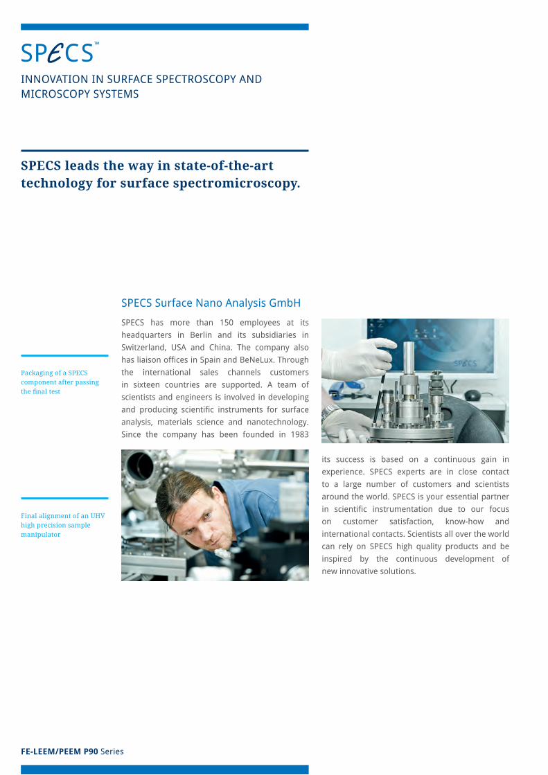
Packaging of a SPECS component after passing the final test
Final alignment of an UHV high precision sample manipulator
SpecS Surface nano analysis GmbH
SpecS has more than 150 employees at its headquarters in Berlin and its subsidiaries in Switzerland, uSa and china. the company also has liaison offices in Spain and BeNeLux. Through the international sales channels customers in sixteen countries are supported. a team of scientists and engineers is involved in developing and producing scientific instruments for surface analysis, materials science and nanotechnology. Since the company has been founded in 1983
its success is based on a continuous gain in experience. SpecS experts are in close contact to a large number of customers and scientists around the world. SpecS is your essential partner in scientific instrumentation due to our focus on customer satisfaction, know-how and international contacts. Scientists all over the world can rely on SpecS high quality products and be inspired by the continuous development of new innovative solutions.
Just a stone’s throw away from the first PEEM’s birthplace, SPECS produces the state-of-the-art instruments with highest resolution.
LEEM/PEEMHIGH reSolutIon electron mIcroScopy of SolId State SurfaceS
History
eighty years ago, Ernst Brüche developed the first photoelectron emission microscope (PEEM) in the aeG laboratories in Berlin. during the following decades the technique developed into a powerful tool for surface science allowing the study of surfaces with a resolution of a few nanometers under illumination of various light sources, such as uv lamps, lasers or synchro-tron radiation. In combination with imaging energy filters laterally resolved photoelectron spectroscopic studies became feasible allowing the study of chemical composition at surfaces with highest spatial resolution.
parallel to the improvements of electron optics Ernst Bauer developed the low energy electron microscopy (LEEM): By equipping the instrument with an electron source and a beam splitter, it became possible to illuminate the sample with a parallel electron beam normal to the surface. those electrons are either elastically backscattered by the sample surface or inelastically scattered under going elementary excitations and producing secondary electrons. In both cases electrons are guided through the same electron optics and via the beam splitter towards the 2-dimensional detector. depending on the primary energy of the incoming and scattered/emitted electrons, and if imaging is done in real or reciprocal space many different
contrast mechanisms can be generated. While low energy electron diffraction (LEED) is an example for crystallographic studies, real space imaging can be done for instance in mirror electron microscopy mode where the incoming electrons are reflected in front of the sample surface.
during the late 20th century, Rudolf Tromp at the IBM Research Division became aware of the possibilities of leem for the in situ observation of deposition processes or phase transitions and began to build a system by himself. the precision in instrument design and high manufacturing quality allowed this instrument to obtain the highest lateral resolution at the time.
as a result SPECS Surface Nano Analysis GmbH, situated in a historic aeG building just a few kilometers away from Brüche’s former laboratory, decided to commercialize tromp’s instrument. By continuous development in collaboration with rudolf tromp at IBm, an aberration correction has been implemented, pushing the resolution limit even further to values below two nanometers.
follow us exploring the nanoworld using the SpecS fe-leem p90.
FE-LEEM/PEEM P90 Series
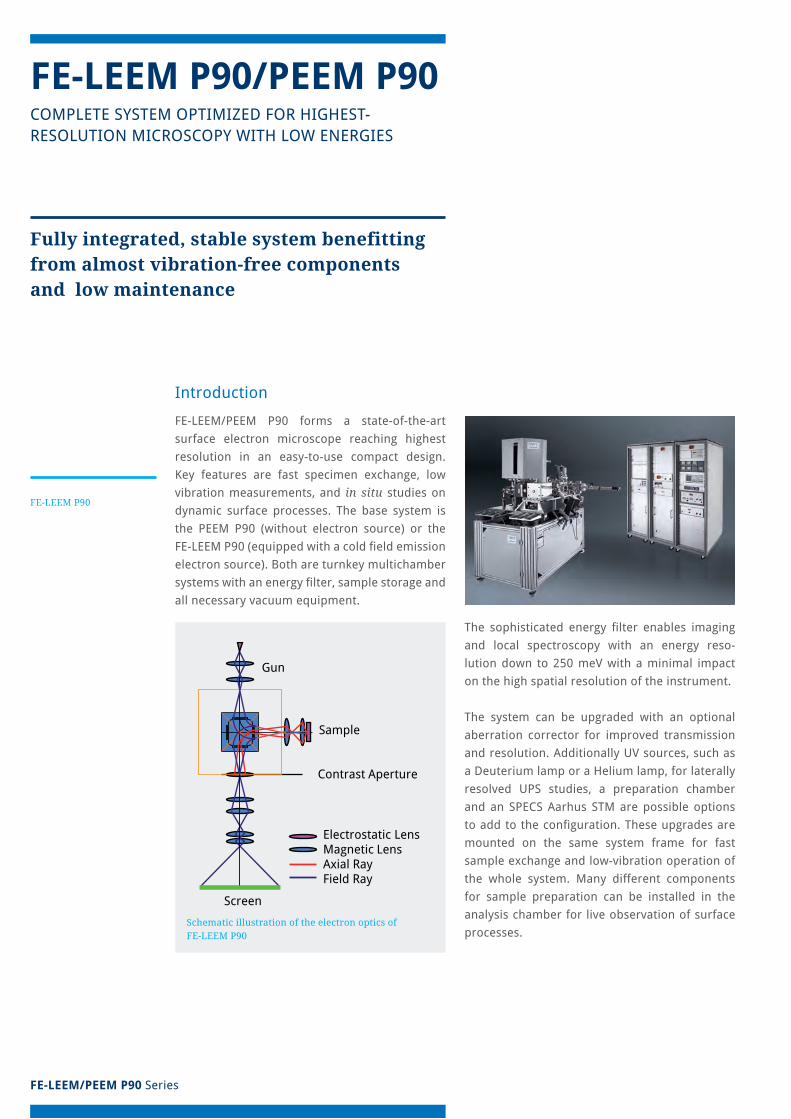
Schematic illustration of the electron optics of FE-LEEM P90
Sample
Contrast Aperture
Gun
Screen
Electrostatic Lens Magnetic LensAxial RayField Ray
complete SyStem optImIzed for HIGHeSt-reSolutIon mIcroScopy WItH loW enerGIeS
Fully integrated, stable system benefitting from almost vibration-free components and low maintenance
FE-LEEM P90/PEEM P90
Introduction
fe-leem/peem p90 forms a state-of-the-art surface electron microscope reaching highest resolution in an easy-to-use compact design.Key features are fast specimen exchange, low vibration measurements, and in situ studies on dynamic surface processes. the base system is the PEEM P90 (without electron source) or the FE-LEEM P90 (equipped with a cold field emission electron source). Both are turnkey multichamber systems with an energy filter, sample storage and all necessary vacuum equipment.
FE-LEEM P90
The sophisticated energy filter enables imaging and local spectroscopy with an energy reso-lution down to 250 mev with a minimal impact on the high spatial resolution of the instrument.
the system can be upgraded with an optional aberration corrector for improved transmission and resolution. additionally uv sources, such as a deuterium lamp or a Helium lamp, for laterally resolved upS studies, a preparation chamber and an SpecS aarhus Stm are possible options to add to the configuration. These upgrades are mounted on the same system frame for fast sample exchange and low-vibration operation of the whole system. Many different components for sample preparation can be installed in the analysis chamber for live observation of surface processes.

5electron optics
the improved optical performance for high-resolution imaging and spectroscopy is based on the energy fi lter and the reduction of electromagnetic infl uences (EMI) at the sample.The 90° magnetic defl ector serves both as a beam splitter for the incoming and outgoing electron beams and as an imaging energy fi lter with an energy resolution of 1.7 ev and < 0.25 ev in imaging and spectroscopy mode, respectively.
all electron optical components are machined to highest precision and mounted in a stacking principle. this ensures the best possible mechanical alignment and allows for operation with a minimum number of electron optical defl ection elements saving valuable time, because the operator does not have to perform additional system alignments. the self-shielded lens design provides an eff ective compensation of external stray fi elds.
As a result of the set-up a large fi eld of view can be obtained ranging from sub-µm to 100 µm which is ideal for overview images as well as for more detailed surface analysis in e.g. domain-like structures.
electron Source
the highest performance in illuminating a sample surface with electrons is achievable with a high-brightness cold fi eld emission gun. the energy spread of < 300 mev is much smaller than in corresponding instruments equipped with thermionic or Schottky emitters. furthermore the high transfer width leads to sharper images, diff raction spots and leed patterns.
uv Sources
Alternative excitation sources can be off ered giving fl exibility to customized measurement techniques at diff erent energy ranges. Light sources such as lasers, helium or deuterium lamps or synchrotron beams can be connected to multiple ports pointing at the sample.
for threshold photoemission microscopy studies the instrument is equipped with a mercury uv source. alternatively the deuterium source duvl 160 can be used.
the high performance ultraviolet Source uvS 300 is ideally suited for ultraviolet photoelectron spectromicroscopy with the integrated energy fi lter. The UV source enables high resolution photoemission measurements with a small spot size and high fl ux density generated by a high density plasma (duo-plasmatron principle). Using a special capillary this source can be focused down to a theoretical spot size of 500 micrometers. Diff erential pumping (50 l/s) enables operation at very low pressures in the analysis chamber (≤ 1 x 10⁻⁸ mbar). The UVS 300 can be mounted on a granite block for eff ective vibration isolation. for application examples please see tromp et al., J. phys.: condens. matter 21 (2009), 314007.
UV source UVS 300
FE-LEEM/PEEM P90 Series
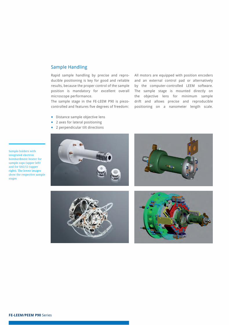
Sample Handling
rapid sample handling by precise and repro-ducible positioning is key for good and reliable results, because the proper control of the sample position is mandatory for excellent overall microscope performance. the sample stage in the fe-leem p90 is piezo-controlled and features fi ve degrees of freedom:
• distance sample objective lens
• 2 axes for lateral positioning
• 2 perpendicular tilt directions
all motors are equipped with position encoders and an external control pad or alternatively by the computer-controlled leem software. the sample stage is mounted directly on the objective lens for minimum sample drift and allows precise and reproducible positioning on a nanometer length scale.
Sample holders with integrated electron bombardment heater for sample caps (upper left) and for SH2/12 (upper right). The lower images show the respective sample stages
7
analysis vacuum chamber
variations to change the sample environment from ultrahigh vacuum (UHV) to in situ conditions are possible at any time according to the goal of the research studies. the system consists of four independently pumped uHv chambers related to the analysis, electron optics, transfer and load lock. this way a vacuum of < 2 x 10⁻¹⁰ mbar can be achieved very fast in
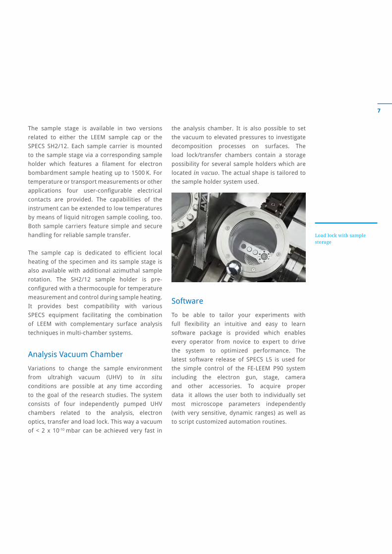
Load lock with sample storage
Software
to be able to tailor your experiments with full flexibility an intuitive and easy to learn software package is provided which enables every operator from novice to expert to drive the system to optimized performance. the latest software release of SpecS l5 is used for the simple control of the fe-leem p90 system including the electron gun, stage, camera and other accessories. to acquire proper data it allows the user both to individually set most microscope parameters independently (with very sensitive, dynamic ranges) as well as to script customized automation routines.
the analysis chamber. It is also possible to set the vacuum to elevated pressures to investigate decomposition processes on surfaces. the load lock/transfer chambers contain a storage possibility for several sample holders which are located in vacuo. the actual shape is tailored to the sample holder system used.
the sample stage is available in two versions related to either the leem sample cap or the SpecS SH2/12. each sample carrier is mounted to the sample stage via a corresponding sample holder which features a filament for electron bombardment sample heating up to 1500 K. for temperature or transport measurements or other applications four user-configurable electrical contacts are provided. the capabilities of the instrument can be extended to low temperatures by means of liquid nitrogen sample cooling, too. Both sample carriers feature simple and secure handling for reliable sample transfer.
The sample cap is dedicated to efficient local heating of the specimen and its sample stage is also available with additional azimuthal sample rotation. the SH2/12 sample holder is pre-configured with a thermocouple for temperature measurement and control during sample heating. It provides best compatibility with various SpecS equipment facilitating the combination of leem with complementary surface analysis techniques in multi-chamber systems.
FE-LEEM/PEEM P90 Series
System frame
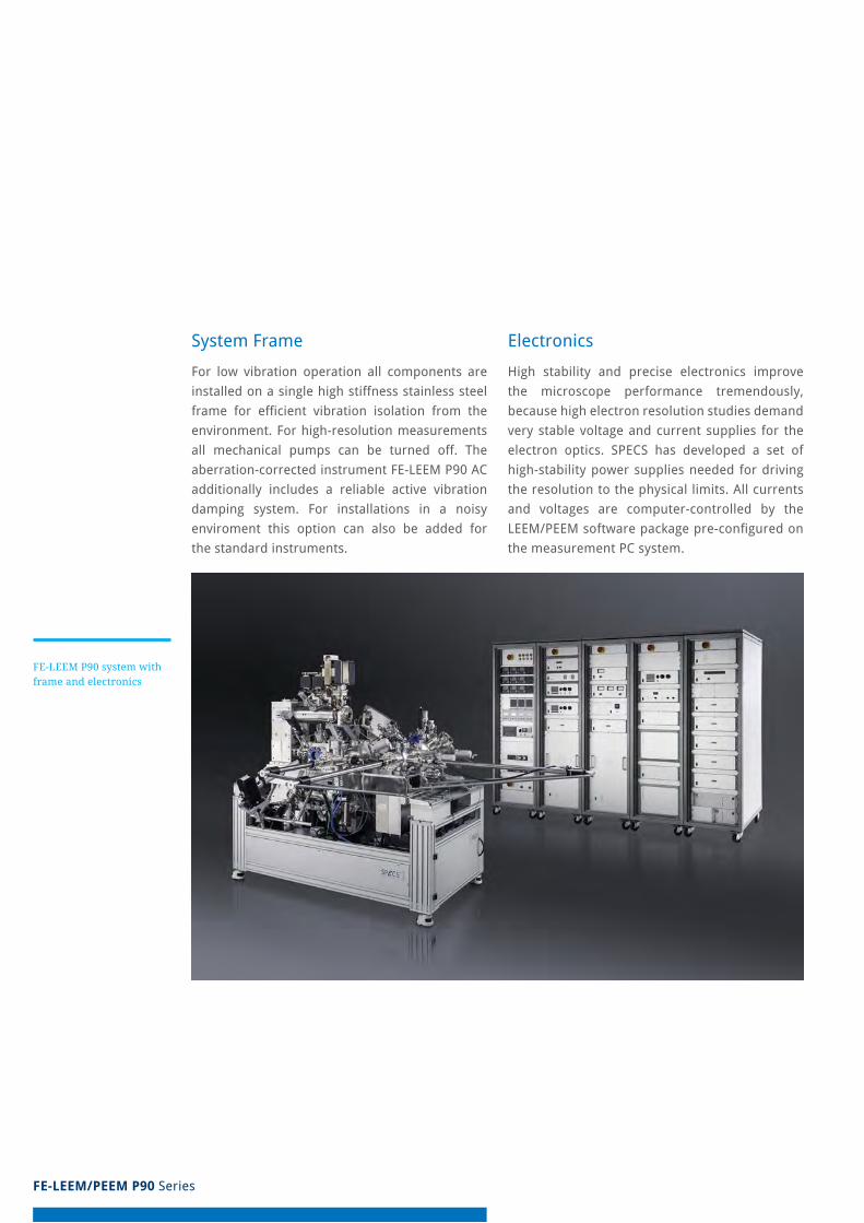
for low vibration operation all components are installed on a single high stiffness stainless steel frame for efficient vibration isolation from the environment. for high-resolution measurements all mechanical pumps can be turned off. The aberration-corrected instrument fe-leem p90 ac additionally includes a reliable active vibration damping system. for installations in a noisy enviroment this option can also be added for the standard instruments.
electronics
High stability and precise electronics improve the microscope performance tremendously, because high electron resolution studies demand very stable voltage and current supplies for the electron optics. SpecS has developed a set of high-stability power supplies needed for driving the resolution to the physical limits. all currents and voltages are computer-controlled by the LEEM/PEEM software package pre-configured on the measurement pc system.
FE-LEEM P90 system with frame and electronics

operation modes
a variety of excitation processes gives access to the structural, chemical, electronic, and magnetic properties of the specimen surface. Using specific operation modes and illumination settings (choice between electrons or photons with variable energy) result in images in which the origin of the contrast formation reveals the actual properties of the investigated sample surface. While photons may excite photoelectrons from core levels and valence states, electrons may result in elastically and inelastically scattered electrons. In addition, both kinds of excitation may result in auger electrons and secondary electrons. depending on the scientific question and complexity of the
problem complementary measurements can be applied. By simply switching between different operation modes correlated information from the same surface area are gained. the magnetic prism transfers both the leem image and the leed pattern stigmatically, allowing routine switching between real image and diffraction. Both image and leed pattern are transferred without the negative effects of chromatic dispersion, offering superior image and diffraction capabilities. The specific operational mode of Mirror Electron Microscopy (MEM), causes almost no sample damage which makes the leem/peem superior in this respect compared to many other conventional analysis instrumentation.
Studying the surface structure benefits from the various applications.
LEEM/PEEMapplIcatIonS of leem and peem
View into analysis chamber: Objective lens with sample stage (right)
Spectroscopy PEEM: UVS 300 mounted to anlysis chamber (left)
FE-LEEM/PEEM P90 Series
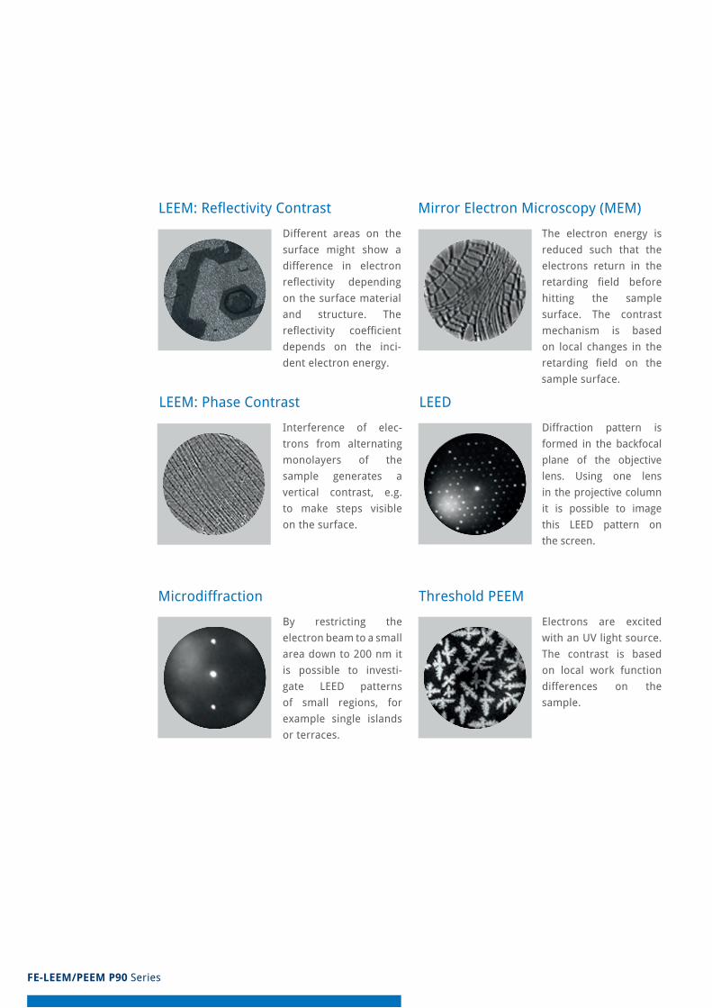
leem: phase contrast
LEEM: Reflectivity Contrast Mirror Electron Microscopy (MEM)
leed
Microdiffraction threshold peem
Different areas on the surface might show a difference in electron reflectivity depending on the surface material and structure. the reflectivity coefficient depends on the inci-dent electron energy.
By restricting the electron beam to a small area down to 200 nm it is possible to investi-gate leed patterns of small regions, for example single islands or terraces.
Interference of elec-trons from alternating monolayers of the sample generates a vertical contrast, e.g. to make steps visible on the surface.
Diffraction pattern is formed in the backfocal plane of the objective lens. using one lens in the projective column it is possible to image this leed pattern on the screen.
electrons are excited with an uv light source. the contrast is based on local work function differences on the sample.
the electron energy is reduced such that the electrons return in the retarding field before hitting the sample surface. the contrast mechanism is based on local changes in the retarding field on the sample surface.
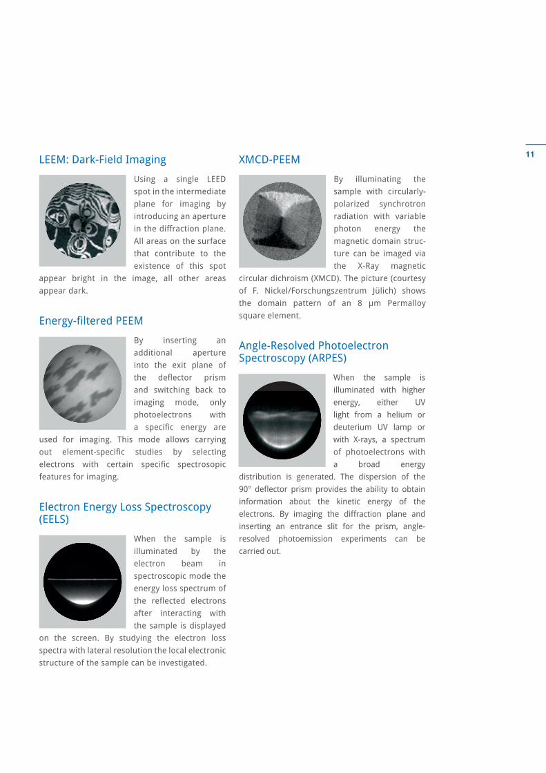
11leem: dark-field Imaging
using a single leed spot in the intermediate plane for imaging by introducing an aperture in the diffraction plane. all areas on the surface that contribute to the existence of this spot
appear bright in the image, all other areas appear dark.
Energy-filtered PEEM
By inserting an additional aperture into the exit plane of the deflector prism and switching back to imaging mode, only photoelectrons with a specific energy are
used for imaging. this mode allows carrying out element-specific studies by selecting electrons with certain specific spectrosopic features for imaging.
electron energy loss Spectroscopy (EELS)
When the sample is illuminated by the electron beam in spectroscopic mode the energy loss spectrum of the reflected electrons after interacting with the sample is displayed
on the screen. By studying the electron loss spectra with lateral resolution the local electronic structure of the sample can be investigated.
angle-resolved photoelectron Spectroscopy (ARPES)
When the sample is illuminated with higher energy, either uv light from a helium or deuterium uv lamp or with X-rays, a spectrum of photoelectrons with a broad energy
distribution is generated. the dispersion of the 90° deflector prism provides the ability to obtain information about the kinetic energy of the electrons. By imaging the diffraction plane and inserting an entrance slit for the prism, angle-resolved photoemission experiments can be carried out.
Xmcd-peem
By illuminating the sample with circularly-polarized synchrotron radiation with variable photon energy the magnetic domain struc-ture can be imaged via the X-ray magnetic
circular dichroism (XMCD). The picture (courtesy of F. Nickel/Forschungszentrum Jülich) shows the domain pattern of an 8 µm permalloy square element.
FE-LEEM/PEEM P90 Series
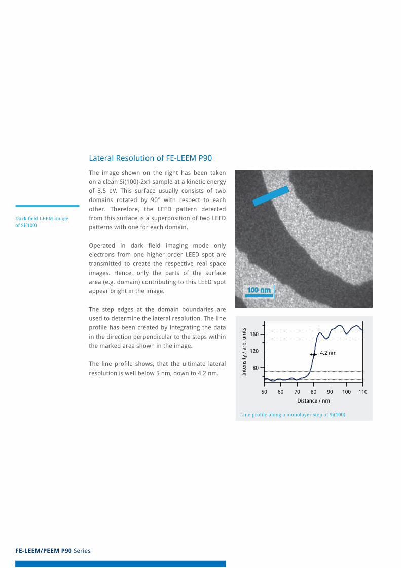
Line profile along a monolayer step of Si(100)
100 nm
lateral resolution of fe-leem p90
the image shown on the right has been taken on a clean Si(100)-2x1 sample at a kinetic energy of 3.5 ev. this surface usually consists of two domains rotated by 90° with respect to each other. therefore, the leed pattern detected from this surface is a superposition of two leed patterns with one for each domain.
Operated in dark field imaging mode only electrons from one higher order leed spot are transmitted to create the respective real space images. Hence, only the parts of the surface area (e.g. domain) contributing to this LEED spot appear bright in the image.
the step edges at the domain boundaries are used to determine the lateral resolution. the line profile has been created by integrating the data in the direction perpendicular to the steps within the marked area shown in the image.
The line profile shows, that the ultimate lateral resolution is well below 5 nm, down to 4.2 nm.
Dark field LEEM image of Si(100)
13
Line profi le along Cu/Ru(0001)
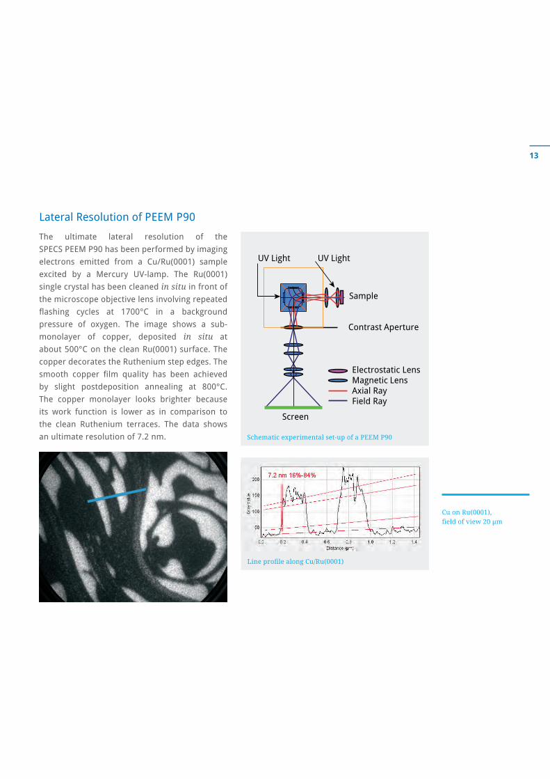
Schematic experimental set-up of a PEEM P90
Sample
UV LightUV Light
Contrast Aperture
Screen
Electrostatic Lens Magnetic LensAxial RayField Ray
lateral resolution of peem p90
the ultimate lateral resolution of the SpecS peem p90 has been performed by imaging electrons emitted from a Cu/Ru(0001) sample excited by a Mercury UV-lamp. The Ru(0001) single crystal has been cleaned in situ in front of the microscope objective lens involving repeated fl ashing cycles at 1700°C in a background pressure of oxygen. the image shows a sub-monolayer of copper, deposited in situ at about 500°C on the clean Ru(0001) surface. The copper decorates the ruthenium step edges. the smooth copper fi lm quality has been achieved by slight postdeposition annealing at 800°c. the copper monolayer looks brighter because its work function is lower as in comparison to the clean ruthenium terraces. the data shows an ultimate resolution of 7.2 nm.
Cu on Ru(0001), fi eld of view 20 μm
FE-LEEM/PEEM P90 Series
Schematic electron optics of the FE-LEEM P90 AC
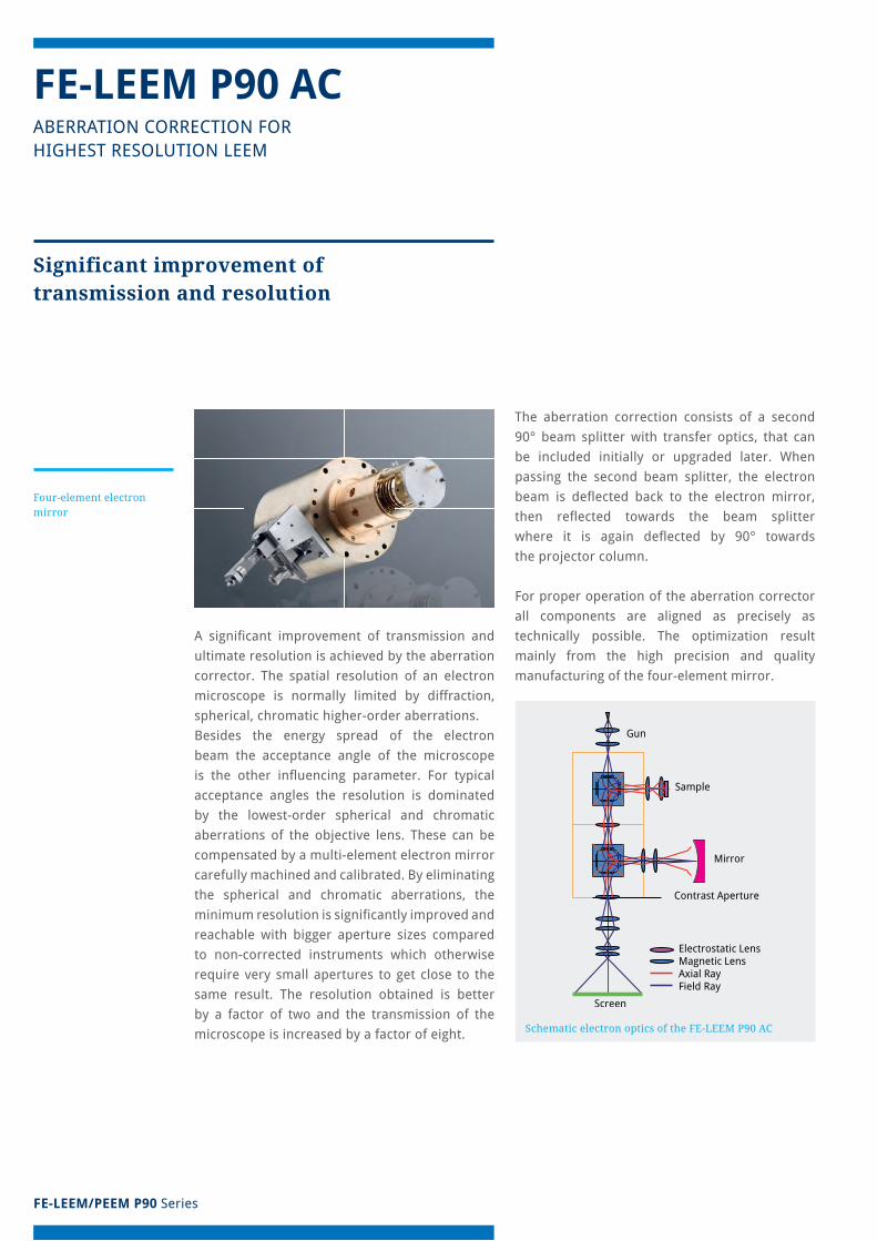
A signifi cant improvement of transmission and ultimate resolution is achieved by the aberration corrector. the spatial resolution of an electron microscope is normally limited by diff raction, spherical, chromatic higher-order aberrations. Besides the energy spread of the electron beam the acceptance angle of the microscope is the other infl uencing parameter. For typical acceptance angles the resolution is dominated by the lowest-order spherical and chromatic aberrations of the objective lens. these can be compensated by a multi-element electron mirror carefully machined and calibrated. By eliminating the spherical and chromatic aberrations, the minimum resolution is signifi cantly improved and reachable with bigger aperture sizes compared to non-corrected instruments which otherwise require very small apertures to get close to the same result. the resolution obtained is better by a factor of two and the transmission of the microscope is increased by a factor of eight.
the aberration correction consists of a second 90° beam splitter with transfer optics, that can be included initially or upgraded later. When passing the second beam splitter, the electron beam is defl ected back to the electron mirror, then refl ected towards the beam splitter where it is again defl ected by 90° towards the projector column.
for proper operation of the aberration corrector all components are aligned as precisely as technically possible. the optimization result mainly from the high precision and quality manufacturing of the four-element mirror.
Significant improvement of transmission and resolution
FE-LEEM P90 ACaBerratIon correctIon for HIGHeSt reSolutIon leem
Four-element electron mirror

15
Line profile along the step of two successive graphene layers
100 nm
Improved lateral resolution of aberration corrected fe-leem p90 acchromatic and spherical aberrations of the objective lens are the limiting factors for the lateral resolution of the fe-leem/peem p90. These limitations can be overcome by reflecting the electrons emitted from a sample with a multi-element electron mirror. this improves the lateral resolution and transmission by a factor of 2 and 8, respectively.
measurements have been performed on thin graphene layers grown on SiC(0001). By flash-annealing the Sic substrate the graphene layers were grown in situ within the leem analysis chamber. the image has been taken from such a graphene layer. Areas with different numbers of carbon layers show different gray levels. Step contrast is seen in areas with the same layer number. The figure to the right shows a step profile and the area where it has been taken. The profile has been averaged over strips (five pixels wide) as indicated in the image by the blue box.
LEEM image of graphene covered SiC(0001)
FE-LEEM/PEEM P90 Series
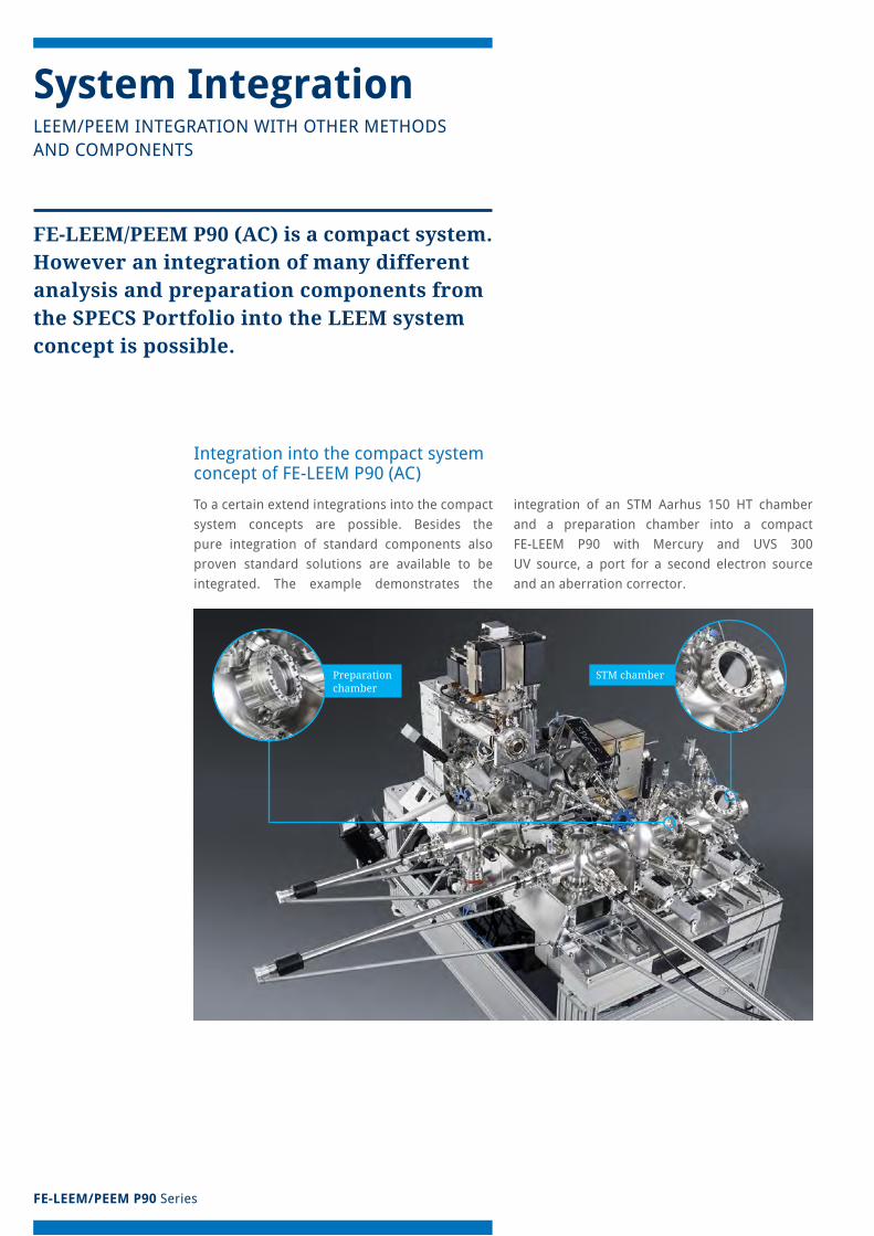
FE-LEEM/PEEM P90 (AC) is a compact system. However an integration of many different analysis and preparation components from the SPECS Portfolio into the LEEM system concept is possible.
System Integrationleem/peem InteGratIon WItH otHer metHodS and componentS
Integration into the compact system concept of FE-LEEM P90 (AC)
to a certain extend integrations into the compact system concepts are possible. Besides the pure integration of standard components also proven standard solutions are available to be integrated. the example demonstrates the
integration of an Stm aarhus 150 Ht chamber and a preparation chamber into a compact fe-leem p90 with mercury and uvS 300 uv source, a port for a second electron source and an aberration corrector.
STM chamberPreparation chamber
17 components for the preparation chamber
Surface modification with subsequent obser- vation of surface processes require the seamless integration of preparation and deposition methods. Sources like the Ion Source IQe 12/38, plasma atom Source mpS-ecr or the multi pocket electron Beam Evaporator EBE-4 can be installed into the preparation chamber or alternatively into the leem/peem analysis chamber for true in situ studies.
components for the Stm aarhus 150 Ht chamber
at highest resolution and stability the SpecS Scanning Tunneling Microscope (STM) allows for observation of processes on surfaces at an atomic scale. the miniaturized design of the STM Aarhus 150 (with the smallest mechanical loop between tip and surface) is unique in the field of commercially available STMs. Fastest scan rates can be achieved by this particular scanner head design. the tip may be cleaned and sharpened inside the Stm with no necessity for tip replacement. a very time saving way of maintaining the quality of the measurements and results. the high temperature version of the Stm aarhus 150 allows for imaging of metals and semiconductors at elevated temperatures up to 1000°c by radiative heating during Stm operation. for this reason the fe-leem p90 and the Spm aarhus 150 Ht perfectly complement each other with respect to an unambiguous interpretation of results. the Stm, integrated into the system, allows for fast sample transfer between Stm and leem without breaking the vacuum.
Multi pocket electron beam evaporator EBE-4 (right image)
MPS-ECS Plasma Source
Ion source IQE 12/38
STM Aarhus 150 (left image)
FE-LEEM/PEEM P90 Series
The compact LEEM/PEEM system itself can also be integrated into larger multimethod system concepts without compromising the performance. Thus an instrument platform with a unique combination of complementary techniques can be designed, with all parts provided from one manufacturer – SPECS.
System Integrationleem/peem InteGratIon Into multImetHod SyStem conceptS
Integration into multimethod System concepts
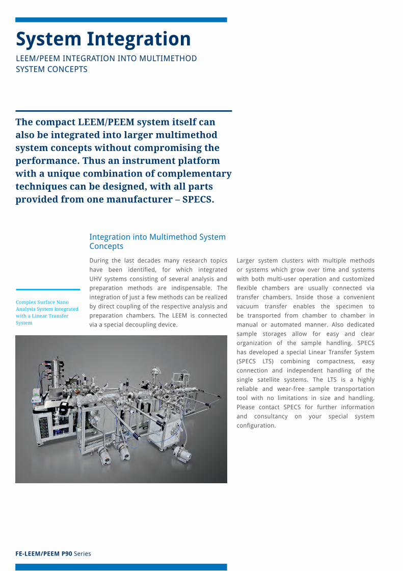
during the last decades many research topics have been identified, for which integrated uHv systems consisting of several analysis and preparation methods are indispensable. the integration of just a few methods can be realized by direct coupling of the respective analysis and preparation chambers. the leem is connected via a special decoupling device.
Complex Surface Nano Analysis System integrated with a Linear Transfer System
larger system clusters with multiple methods or systems which grow over time and systems with both multi-user operation and customized flexible chambers are usually connected via transfer chambers. Inside those a convenient vacuum transfer enables the specimen to be transported from chamber to chamber in manual or automated manner. also dedicated sample storages allow for easy and clear organization of the sample handling. SpecS has developed a special linear transfer System (SPECS LTS) combining compactness, easy connection and independent handling of the single satellite systems. the ltS is a highly reliable and wear-free sample transportation tool with no limitations in size and handling. please contact SpecS for further information and consultancy on your special system configuration.

19
Dimensions of FE-LEEM P90 AC
Dimensions of FE-LEEM P90 AC
FE-LEEM/PEEM P90 Series
resolution with fe-leem p90
Guaranteed: 5 nm, Achieved: 4.2 nm
resolution with fe-leem p90 ac
Guaranteed: 2 nm, achieved: 1.6 nm
field of view 800 nm – 100 µm
Magnification 400x – 50000x
energy resolution Spectroscopy: < 250 mevImaging: < 1.7 ev
Kinetic energy in the microscope
typically 15 kev,scaleable down to 2 kev
Start energy up to 1000 ev
Base pressure Better than 2 x 10⁻¹⁰ mbar
leem spot size< 40 µm down to 200 nm with micro-diffraction aperture
energy width of illumination beam < 300 mev
reproducibility of sample position Better than 500 nm
maximum temperature for imaging 1500 K
Technical Data
Specifications
SPECS Surface nano analysis GmbH voltastrasse 513355 Berlin / Germany www.specs.com
T +49 30 46 78 24-0F +49 30 46 42 083e [email protected]