failure analysis: the right way - dfrsolutions.com · failure rate during in-process testing....
TRANSCRIPT
i
i
Failure Analysis: The Right Way
Counterfeit Diode Investigation
DfR Staff
5110 Roanoke Place, Suite 101, College Park, Maryland 20740 | Phone: (301) 474-0607 | Fax: (866) 247-9457 | www.dfrsolutions.com
Introduction1
A DfR customer received diodes through broker distribution channels that had shown a very high failure rate during in-process testing. Testing of “as received” diodes showed a significant portion of the diodes did not meet their data sheet reverse breakdown voltage and reverse current specifications. Failure analysis on sample diodes that did not meet their electrical characteristics indicated high current stress damage. In-house diodes were screened electrically for reverse breakdown voltage/leakage current. A sample of 24 diodes that passed this screening was subjected to a Steady State Operation Life test in accordance with MIL-PRF-19500/477G, Para. 4.4.3.1 and Mil Std 750 Method 1026. The sample of 24 diodes was initially checked for electrical performance per group A (reverse breakdown voltage, reverse current, forward voltage drop at 4A pulse and forward voltage drop at 6A pulse). All diodes passed. At 250 hours into the 1000 hour steady state life test the test articles were subject to an interim group A electrical test. At that point diode D21 was reported as failed.
Experimental Procedure
The failed diode was subjected to the following analyses:
X-ray Imaging
Electrical Characterization
Decapsulation, Cross-Sectioning with Optical Microscopy was performed to inspect the die for damages
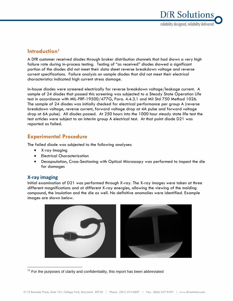
X-ray imaging Initial examination of D21 was performed through X-ray. The X-ray images were taken at three different magnifications and at different X-ray energies, allowing the viewing of the molding compound, the insulation and the die as well. No definitive anomalies were identified. Example images are shown below.
11
For the purposes of clarity and confidentiality, this report has been abbreviated
5110 Roanoke Place, Suite 101, College Park, Maryland 20740 | Phone: (301) 474-0607 | Fax: (866) 247-9457 | www.dfrsolutions.com
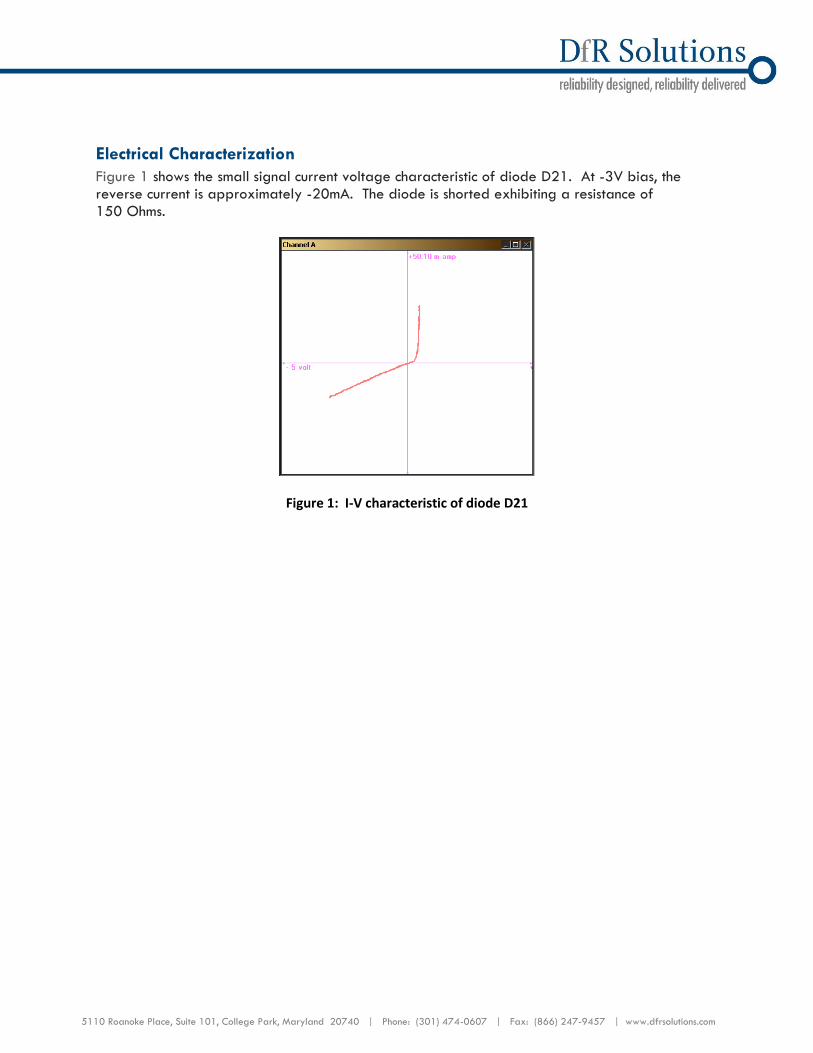
Electrical Characterization
Figure 1 shows the small signal current voltage characteristic of diode D21. At -3V bias, the reverse current is approximately -20mA. The diode is shorted exhibiting a resistance of 150 Ohms.
Figure 1: I-V characteristic of diode D21
5110 Roanoke Place, Suite 101, College Park, Maryland 20740 | Phone: (301) 474-0607 | Fax: (866) 247-9457 | www.dfrsolutions.com
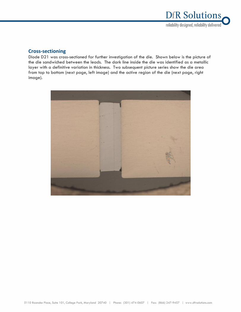
Cross-sectioning Diode D21 was cross-sectioned for further investigation of the die. Shown below is the picture of the die sandwiched between the leads. The dark line inside the die was identified as a metallic layer with a definitive variation in thickness. Two subsequent picture series show the die area from top to bottom (next page, left image) and the active region of the die (next page, right image).
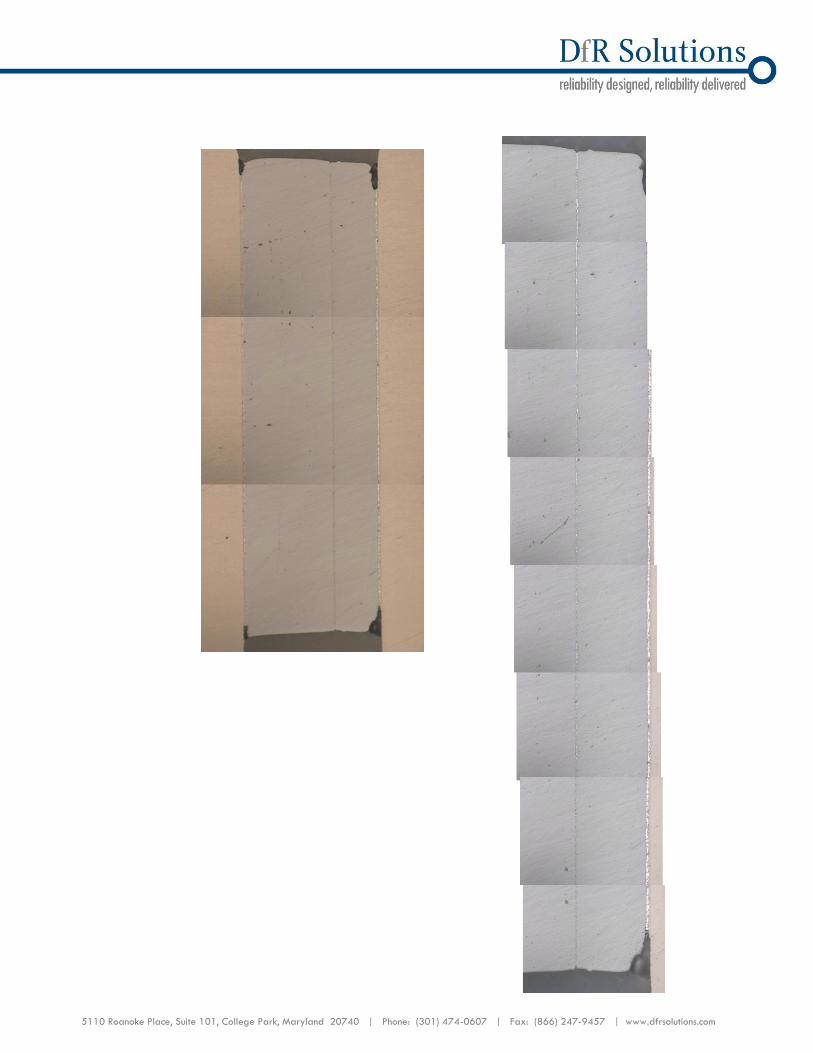
5110 Roanoke Place, Suite 101, College Park, Maryland 20740 | Phone: (301) 474-0607 | Fax: (866) 247-9457 | www.dfrsolutions.com
5110 Roanoke Place, Suite 101, College Park, Maryland 20740 | Phone: (301) 474-0607 | Fax: (866) 247-9457 | www.dfrsolutions.com
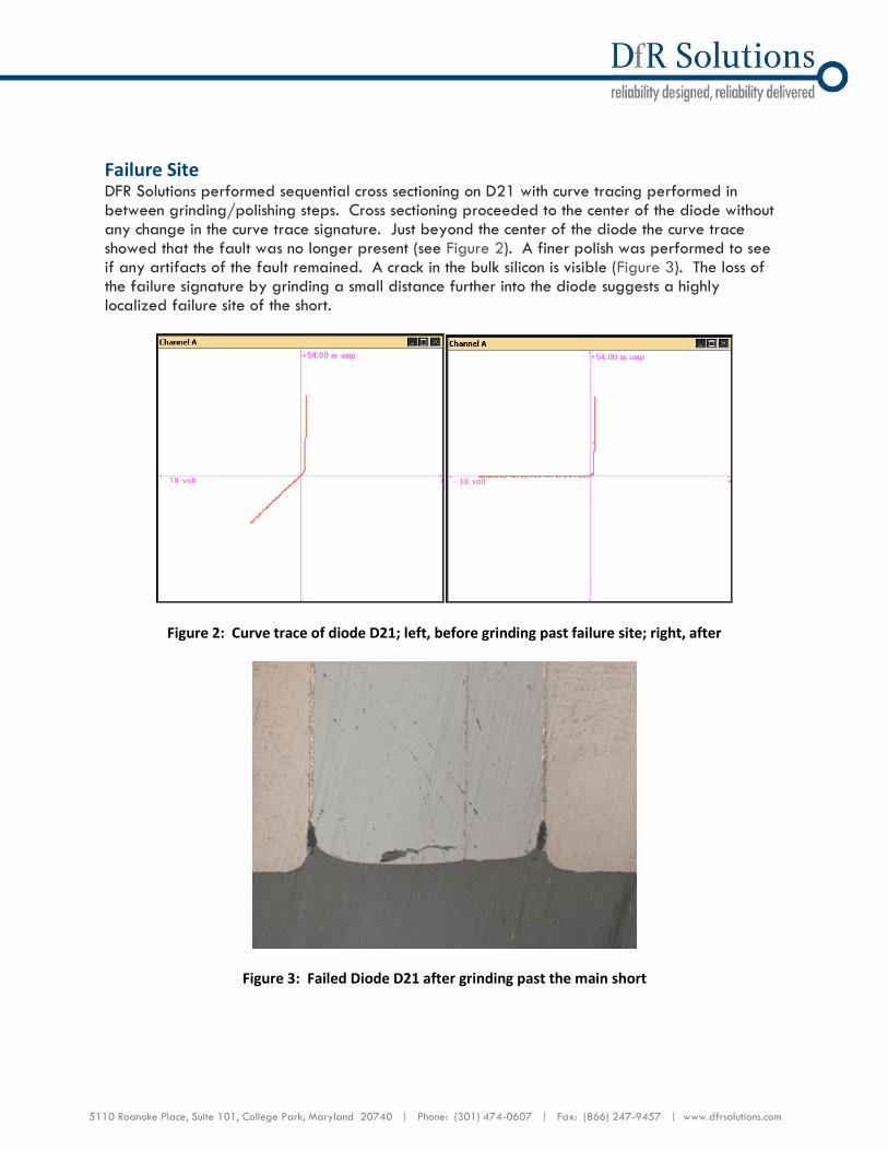
Failure Site DFR Solutions performed sequential cross sectioning on D21 with curve tracing performed in between grinding/polishing steps. Cross sectioning proceeded to the center of the diode without any change in the curve trace signature. Just beyond the center of the diode the curve trace showed that the fault was no longer present (see Figure 2). A finer polish was performed to see if any artifacts of the fault remained. A crack in the bulk silicon is visible (Figure 3). The loss of the failure signature by grinding a small distance further into the diode suggests a highly localized failure site of the short.
Figure 2: Curve trace of diode D21; left, before grinding past failure site; right, after
Figure 3: Failed Diode D21 after grinding past the main short

5110 Roanoke Place, Suite 101, College Park, Maryland 20740 | Phone: (301) 474-0607 | Fax: (866) 247-9457 | www.dfrsolutions.com
The diode — with approximately half of the area still present — still exhibited a high reverse
leakage current of -370μA at -160V (see Figure 4). This indicates the presence of a distribution of failure sites across the die, of which one failed catastrophically.
Figure 4: Measurements of reverse leakage current after grinding past failure site
Electron Microscopy
Energy dispersive spectroscopy (EDS) performed during examination by electron microscopy identified silver as the primary element in the metallic layer. A small amount of gold was also identified. As can be seen in the figure to the right, gold energy
transition peaks at 2.120 keV (Au Mα) and at
9.710 keV (Au Lα1) are evident in “Spectrum 3” and “Spectrum 2”. The image resolution of “Spectrum 1” is unfortunately insufficient to clearly prove the presence
of gold in the silicon, but the Au Mα peak seems to be present. Gold is known to be used as a dopant in fast-recovery diodes. While contamination of silver does not necessarily lead to a strong degradation of the diode properties, contamination with gold is known to degrade the junction performance severely. .
Reverse Bias Diode D21
-5.00E-04
-4.50E-04
-4.00E-04
-3.50E-04
-3.00E-04
-2.50E-04
-2.00E-04
-1.50E-04
-1.00E-04
-5.00E-05
0.00E+00
-180 -160 -140 -120 -100 -80 -60 -40 -20 0
Voltage (V)
Cu
rren
t (A
)
Diode D21
after grinding past the main failure site
5110 Roanoke Place, Suite 101, College Park, Maryland 20740 | Phone: (301) 474-0607 | Fax: (866) 247-9457 | www.dfrsolutions.com
Metal contamination
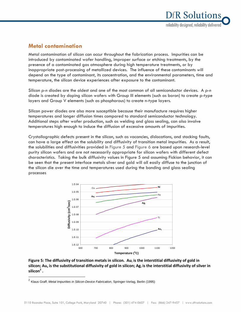
Metal contamination of silicon can occur throughout the fabrication process. Impurities can be introduced by contaminated wafer handling, improper surface or etching treatments, by the presence of a contaminated gas atmosphere during high temperature treatments, or by inappropriate post-processing of metallized devices. The influence of these contaminants will depend on the type of contaminant, its concentration, and the environmental parameters, time and temperature, the silicon device experiences after exposure to the contaminant. Silicon p-n diodes are the oldest and one of the most common of all semiconductor devices. A p-n diode is created by doping silicon wafers with Group III elements (such as boron) to create p-type layers and Group V elements (such as phosphorous) to create n-type layers. Silicon power diodes are also more susceptible because their manufacture requires higher temperatures and longer diffusion times compared to standard semiconductor technology. Additional steps after wafer production, such as welding and glass sealing, can also involve temperatures high enough to induce the diffusion of excessive amounts of impurities. Crystallographic defects present in the silicon, such as vacancies, dislocations, and stacking faults, can have a large effect on the solubility and diffusivity of transition metal impurities. As a result, the solubilities and diffusivities provided in Figure 5 and Figure 6 are based upon research-level purity silicon wafers and are not necessarily appropriate for silicon wafers with different defect characteristics. Taking the bulk diffusivity values in Figure 5 and assuming Fickian behavior, it can be seen that the present interface metals silver and gold will all easily diffuse to the junction of the silicon die over the time and temperatures used during the bonding and glass sealing processes
Figure 5: The diffusivity of transition metals in silicon. Aui is the interstitial diffusivity of gold in silicon; Aus is the substitutional diffusivity of gold in silicon; Agi is the interstitial diffusivity of silver in silicon2 .
2 Klaus Graff, Metal Impurities in Silicon-Device Fabrication, Springer-Verlag, Berlin (1995)
1.E-12
1.E-11
1.E-10
1.E-09
1.E-08
1.E-07
1.E-06
1.E-05
1.E-04
600 700 800 900 1000 1100 1200
Temperature (oC)
Dif
fus
ivit
y (
cm
2/s
ec
)
Cu Ni
Aui
Fe
Agi
Ti
Aus
5110 Roanoke Place, Suite 101, College Park, Maryland 20740 | Phone: (301) 474-0607 | Fax: (866) 247-9457 | www.dfrsolutions.com
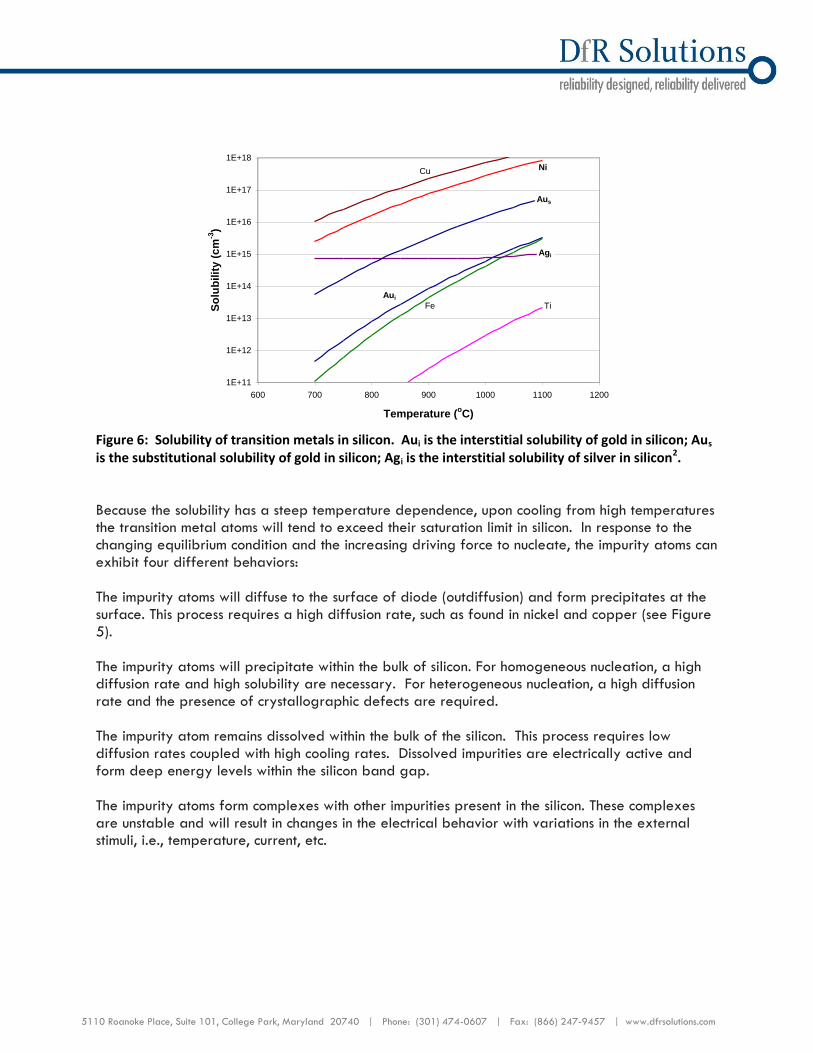
Figure 6: Solubility of transition metals in silicon. Aui is the interstitial solubility of gold in silicon; Aus is the substitutional solubility of gold in silicon; Agi is the interstitial solubility of silver in silicon2. Because the solubility has a steep temperature dependence, upon cooling from high temperatures the transition metal atoms will tend to exceed their saturation limit in silicon. In response to the changing equilibrium condition and the increasing driving force to nucleate, the impurity atoms can exhibit four different behaviors: The impurity atoms will diffuse to the surface of diode (outdiffusion) and form precipitates at the surface. This process requires a high diffusion rate, such as found in nickel and copper (see Figure 5). The impurity atoms will precipitate within the bulk of silicon. For homogeneous nucleation, a high diffusion rate and high solubility are necessary. For heterogeneous nucleation, a high diffusion rate and the presence of crystallographic defects are required. The impurity atom remains dissolved within the bulk of the silicon. This process requires low diffusion rates coupled with high cooling rates. Dissolved impurities are electrically active and form deep energy levels within the silicon band gap. The impurity atoms form complexes with other impurities present in the silicon. These complexes are unstable and will result in changes in the electrical behavior with variations in the external stimuli, i.e., temperature, current, etc.
1E+11
1E+12
1E+13
1E+14
1E+15
1E+16
1E+17
1E+18
600 700 800 900 1000 1100 1200
Temperature (oC)
So
lub
ilit
y (
cm
-3)
Cu Ni
Aui
Fe
Agi
Ti
Aus
5110 Roanoke Place, Suite 101, College Park, Maryland 20740 | Phone: (301) 474-0607 | Fax: (866) 247-9457 | www.dfrsolutions.com
The following paragraphs will review the influence of silver, and gold on the electrical properties of p-n diodes.
Silver
Silver is also a fast diffuser in silicon (see Figure 5). Silver acts as a singly ionizable donor in p- and n-type silicon. In p-type silicon, the donor level is 0.26eV above the valence band; in n-type silicon, the acceptor level is 0.29eV below the conduction band. Previous work has found that at room temperature. Because the capture cross-section at room temperature for silver atoms is low[2], carrier mobilities and carrier lifetimes in silicon diodes are relatively unaffected by the introduction of large concentrations of silver.
Gold
Because gold acts as a strong recombination center in silicon, it has been widely used as a dopant to control minority carrier lifetime and improve the speed of semiconductor devices. However, the unintended doping of silicon with gold can lead to the degradation of important electrical properties. Tolerable gold impurity content during wafer production is often much less than 1012 cm-3, which necessitates the use of Deep Level Transient Spectroscopy (DLTS) for impurity detection. Concerns about gold impurity have led to stricter quality control during wafer processing and replacement of gold as a rear contact material. These steps have led to a reduction in the frequency of excessive gold contamination. The contamination of silicon with gold is easily performed by the mechanical contact of gold with silicon because gold rapidly migrates into silicon, even at low temperatures (< 800°C). As an example, Mielke3 and Makhkamov4 measured a three orders of magnitude increase in the gold concentration in silicon, from 1010 cm-3 to approximately 1013 cm-3, after a heat treatment of 800°C for one hour. This high diffusion rate is in part due to the formation of a gold-silicon eutectic at 370°C. With increasing temperatures, this liquid phase acts as a rapid diffusion source. Gold diffusion in silicon occurs by an interstitial-substitutional process. The diffusivity of interstitial gold is very high while the solubility is low. The reverse is true for substitutional gold, which has a low diffusivity and a high solubility5. The net result is that the diffusive flux is carried almost entirely by interstitial diffusion. The interstitials can then combine with vacancies in the silicon lattice to form substitutional defects. These substitutional gold defects are electrically active and will tend to have the greatest effect on the electrical properties of the p-n diode.
[2] Two orders of magnitude lower than gold. 3 W. Mielke, "Penentration of Gold and Platinum Through Phosphorous-Doped N+ Layers in Silicon," Journal of the Electrochemical Society, vol. 122, no. 7, pp. 965-969 (1975) 4 S. Makhkamov, N.A. Tursunov, M. Mamanova, and M. Ashurov, "The Effect of a New Gold Center on the Characteristics of Silicon Diodes," Soviet Tech. Phys. Letters, vol. 17, no. 12, pp. 887-889 (1991) 5 Substitutional gold diffusion and solubility is strongly dependent upon crystal perfection and the presence other defects. As a result, diffusivity and solubility measurements for homogeneous silicon cannot be applied indiscriminately to silicon with other defect characteristics or to all regions of a particular device.
5110 Roanoke Place, Suite 101, College Park, Maryland 20740 | Phone: (301) 474-0607 | Fax: (866) 247-9457 | www.dfrsolutions.com
Gold tends to have a greater influence on junction behavior than other transition metals, because the position of acceptor energy level for substitutional gold in n-type silicon, -0.54eV below the conduction band edge or in the middle of the band gap, makes gold a very effective recombination center. In addition, since gold introduces both a deep donor and acceptor in silicon, it decreases the net carrier concentration in both p-type and n-type material. Gold can also combine with iron impurities already present in the silicon crystal to create iron-gold complexes. These iron-gold complexes form between 200-300°C and can result in a reduction in the carrier lifetime by a factor of five in comparison to substitutional gold of equal concentration. It is therefore important to avoid the formation of iron-gold pairs. This requires avoiding gold contamination, since iron is almost always present in silicon wafers, at least in low concentrations. A summary of previous work on the effect of gold on the electrical properties of silicon diodes is provided below:
Resisitivity
Gold increases the resistivity of silicon diodes by decreasing the net carrier concentration6.
Reverse Leakage Current
The leakage current in gold doped silicon can be estimated from I = qWANtetp , where q is the
electronic charge, W is the depletion width, A is the area of the diode, Nt is the gold concentration, and et
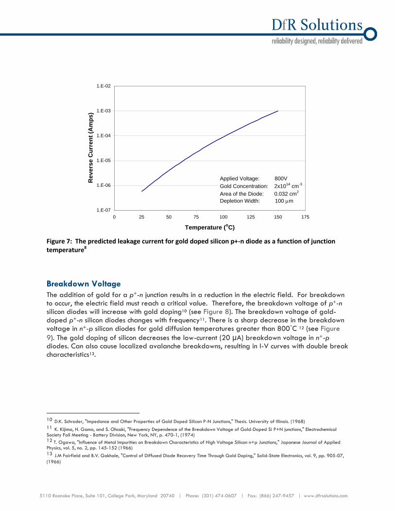
p is the thermal emission rate of holes from neutral acceptors7,8 (see Figure 7). The reverse current at 1000V at 180°C was found to increase from 4 mA to 130 mA after diffusing gold into silicon at 865°C. Diffusion time and gold concentration were not provided9. Due to increases in the leakage current with increasing temperature, for a gold dopant level of 2x1014 cm-3, silicon p+-n diodes will become unstable at 150°C 8.
6 E.D. Wolley and R. Stickler, "Formation of Precipitates in Gold Diffused Silicon," Journal of Electrochemical Society, vol. 114, no. 12, pp. 1287-92 (1967) 7 W.M. Bullis, "Properties of Gold in Silicon," Solid-State Electronics, vol. 9, pp. 143-168 (1966).
8 M.D. Miller, "Differences Between Platinum- and Gold-Doped Silicon Power Devices," IEEE Trans. Electron Devices, vol. ED-23, no. 12, p. 1279-83, (1976) 9 B.J. Baliga and E. Sun, "Comparison of Gold, Platinum, and Electron Irradiation for Controlling Lifetime in Power Rectifiers," IEEE Trans. Electron Devices, vol. ED-24, no. 6, p. 685-8, (1977)
5110 Roanoke Place, Suite 101, College Park, Maryland 20740 | Phone: (301) 474-0607 | Fax: (866) 247-9457 | www.dfrsolutions.com
Figure 7: The predicted leakage current for gold doped silicon p+-n diode as a function of junction temperature8
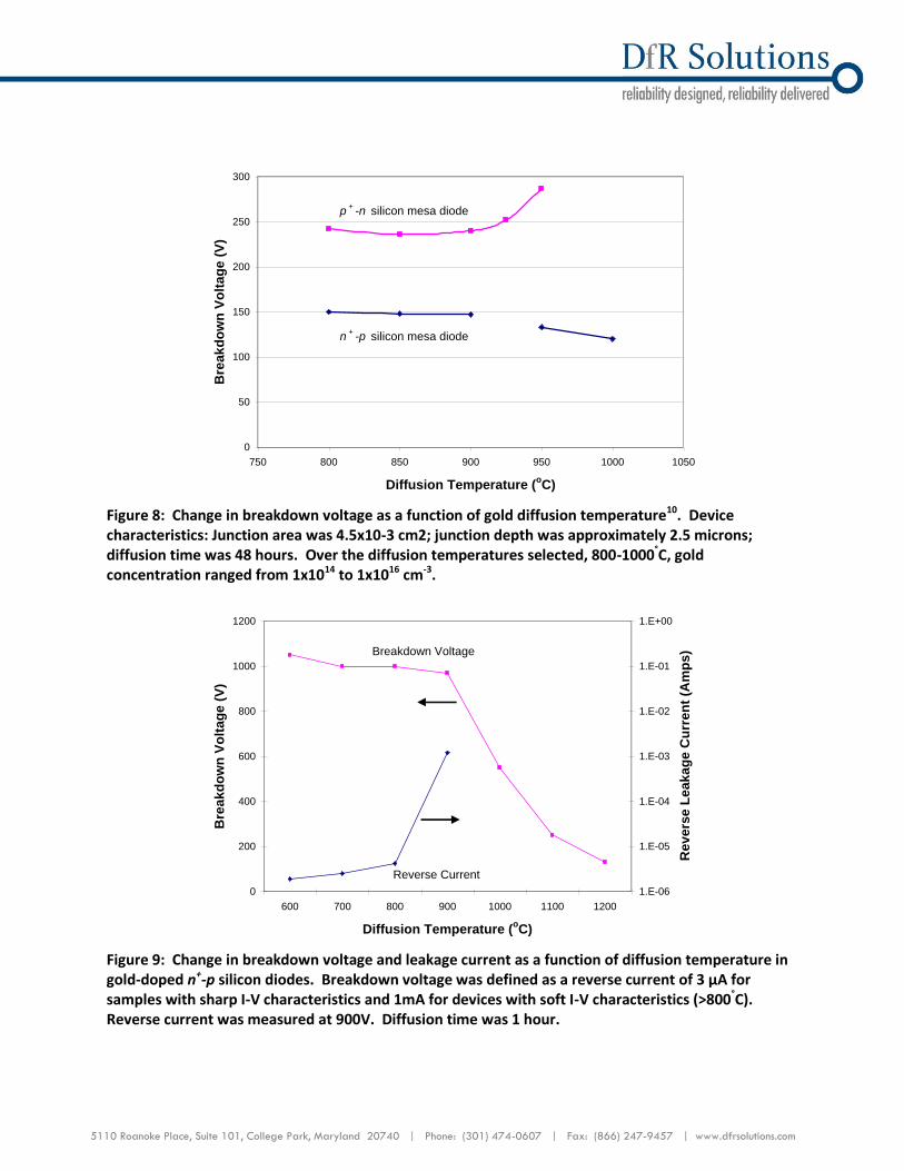
Breakdown Voltage
The addition of gold for a p+-n junction results in a reduction in the electric field. For breakdown to occur, the electric field must reach a critical value. Therefore, the breakdown voltage of p+-n silicon diodes will increase with gold doping10 (see Figure 8). The breakdown voltage of gold-doped p+-n silicon diodes changes with frequency11. There is a sharp decrease in the breakdown voltage in n+-p silicon diodes for gold diffusion temperatures greater than 800°C 12 (see Figure
9). The gold doping of silicon decreases the low-current (20 μA) breakdown voltage in n+-p diodes. Can also cause localized avalanche breakdowns, resulting in I-V curves with double break characteristics13.
10 D.K. Schroder, "Impedance and Other Properties of Gold Doped Silicon P-N Junctions," Thesis. University of Illinois. (1968)
11 K. Kijima, H. Gamo, and S. Ohsaki, "Frequency Dependence of the Breakdown Voltage of Gold-Doped Si P+N junctions," Electrochemical Society Fall Meeting - Battery Division, New York, NY, p. 470-1, (1974) 12 T. Ogawa, "Influence of Metal Impurities on Breakdown Characteristics of High Voltage Silicon n+p Junctions," Japanese Journal of Applied Physics, vol. 5, no. 2, pp. 145-152 (1966)
13 J.M Fairfield and B.V. Gokhale, "Control of Diffused Diode Recovery Time Through Gold Doping," Solid-State Electronics, vol. 9, pp. 905-07,
(1966)
1.E-07
1.E-06
1.E-05
1.E-04
1.E-03
1.E-02
0 25 50 75 100 125 150 175
Temperature (oC)
Rev
ers
e C
urr
en
t (A
mp
s)
Applied Voltage: 800V
Gold Concentration: 2x10¹⁴
cm-3
Area of the Diode: 0.032 cm2
Depletion Width: 100 m
5110 Roanoke Place, Suite 101, College Park, Maryland 20740 | Phone: (301) 474-0607 | Fax: (866) 247-9457 | www.dfrsolutions.com
Figure 8: Change in breakdown voltage as a function of gold diffusion temperature10. Device characteristics: Junction area was 4.5x10⁻³ cm2; junction depth was approximately 2.5 microns; diffusion time was 48 hours. Over the diffusion temperatures selected, 800-1000°C, gold concentration ranged from 1x10¹⁴ to 1x1016 cm-3.
Figure 9: Change in breakdown voltage and leakage current as a function of diffusion temperature in gold-doped n+-p silicon diodes. Breakdown voltage was defined as a reverse current of 3 µA for samples with sharp I-V characteristics and 1mA for devices with soft I-V characteristics (>800°C). Reverse current was measured at 900V. Diffusion time was 1 hour.
0
50
100
150
200
250
300
750 800 850 900 950 1000 1050
Diffusion Temperature (oC)
Bre
ak
do
wn
Vo
ltag
e (
V)
p+
-n silicon mesa diode
n+
-p silicon mesa diode
0
200
400
600
800
1000
1200
600 700 800 900 1000 1100 1200
Diffusion Temperature (oC)
Bre
ak
do
wn
Vo
ltag
e (
V)
1.E-06
1.E-05
1.E-04
1.E-03
1.E-02
1.E-01
1.E+00
Rev
ers
e L
eak
ag
e C
urr
en
t (A
mp
s)Breakdown Voltage
Reverse Current
5110 Roanoke Place, Suite 101, College Park, Maryland 20740 | Phone: (301) 474-0607 | Fax: (866) 247-9457 | www.dfrsolutions.com
Forward Current
Forward current is also dependent upon gold concentration. The dependency is linear or square root depending if low current or high current densities7.
Junction Capacitance
The transition capacitance of silicon p-n diodes is frequency independent. When gold is added, the junction capacitance of gold-doped p+-n diodes becomes frequency dependent14 and varies with gold concentration10.
14 C.T. Sah and V.G. Reddi, Transactions of the Institute of Electrical and Electronic Engineers, vol. ED-11, pp. 345 (1964)
5110 Roanoke Place, Suite 101, College Park, Maryland 20740 | Phone: (301) 474-0607 | Fax: (866) 247-9457 | www.dfrsolutions.com
Summary
Cross-sectioning of the diode showed the failure sites being distributed across the die, with a
catastrophic failure (150Ω) occurring very localized at one of those sites. A review of the EDS data shows the presence of silver and gold close to the diode region. The silver is present in the die attach between the two dies, which is expected as silver is a common conductor in commercial die attach material. Since gold is frequently used as a dopant for fast recovery diodes, it is not clear whether the gold is present as part of the silver attach or as a dopant. Gold is known to diffuse easily into the p-n region of a diode. The effects of gold contamination are among others reduction in reverse breakdown voltage and increased reverse leakage current, as well as increase in forward bias resistivity. Given the evidence of multiple failure sites, the presence of gold is the likely root-cause of diode failure and its presence in the critical regions of the die should be confirmed through the use of secondary ion mass spectroscopy (SIMS)
5110 Roanoke Place, Suite 101, College Park, Maryland 20740 | Phone: (301) 474-0607 | Fax: (866) 247-9457 | www.dfrsolutions.com
Disclaimer
DfR represents that a reasonable effort has been made to ensure the accuracy and reliability of the information within this report. However, DfR Solutions makes no warranty, both express and implied, concerning the content of this report, including, but not limited to the existence of any latent or patent defects, merchantability, and/or fitness for a particular use. DfR will not be liable for loss of use, revenue, profit, or any special, incidental, or consequential damages arising out of, connected with, or resulting from, the information presented within this report.
Confidentiality
The information contained in this document is considered to be proprietary to DfR Solutions and the appropriate recipient. Dissemination of this information, in whole or in part, without the prior written authorization of DfR Solutions, is strictly prohibited.