fabrication and assembly of multi-layered microstructures...
TRANSCRIPT

Abstract—Recently the research about constructing 3 dimensional cell structures is very important for its great potential applications in tissue engineering. In this paper, we report a novel method of constructing multi-layered microstructures embedding cells via microfluidic devices. The on-chip fabrication of movable microstructures embedding fibroblasts (NIH/3T3) based on Poly (ethylene glycol) Diacrylate (PEGDA) was reported. Two approaches for assembling these movable microstructures were presented. One was a manual assembly method based on micromanipulation system and the other one was a self-assembly method based on microfluidic channel. Several manual assembly ways were demonstrated and a tube-shaped microstructure with 17 layers was assembled by an efficient assembly method. A novel microfluidic channel was presented for conducting self-assembly method and a 2-layered experimental microfluidic device was fabricated by Polydimethylsiloxane (PDMS). The self-assembly process of fabricated microstructures via this device was preliminarily demonstrated.
I. INTRODUCTION
ecently the research about constructing 3 dimensional cell structures is very important, since it can provide effective approaches of constructing implantable in vitro
artificial tissue for tissue engineering [1]. The cells inside real tissues and organs are arranged according to certain shapes, such as neural cells with line shape, skin with reticular shape and blood vessel with tube shape [2]. For building artificial tissues, important issues are how to immobilize cells inside certain structures for encapsulation and how to assemble these structures to form different shapes as cell scaffolds [3, 4]. Moreover, long-term co-culture of these immobilized and assembled cells is the key way to construct functional artificial tissues [5].
The current methods for cell immobilization are based on such as aspiration, pressure of solution and fluidic structure [6]. The advantage of aspiration and pressure is that fixing force is large, while the disadvantage is damaging the cells [7]. By special fluidic structures, cell is immobilized inside microfluidic device. The immobilized cells are difficult to be further analysis [8]. On-chip fabrication based on Tao Yue, Masahiro Nakajima, Huaping Wang, Chengzhi Hu and Toshio Fukuda are with Department of Micro-Nano Systems Engineering, Nagoya University, Furo-cho, Chikusa-ku, Nagoya, 464-8603 JAPAN ( e-mail: [email protected])
Huaping Wang and Toshio Fukuda are with School of Mechatronic Engineering, Beijing Institute of Technology, 5 South Zhongguancun Street, Haidian District, Beijing, 100081 CHINA
Toshio Fukuda is with the Faculty of Science and Engineering, Meijo University, Nagoya, JAPAN.
photo-crosslinkable resin via UV illumination is a creative way for immobilizing cells [9]. Cells are directly immobilized inside the microfluidic device. Several advantages such as high-speed, low-cost and arbitrary shaped are with the on-chip fabrication method [10].
There are several methods for assembling 3 dimensional (3D) cell structures. Scaffolds are used for holding cells to generate complex and arbitrary 3D structures [11]. However, the cell embedding and growth inside the scaffolds are still not efficient. Constructing 3D structures after cell encapsulation is a good idea for building 3D cell structures. Hydrogel fiber embedding several kinds of cells and co-culture of them is demonstrated [12]. Shape of these hydrogels is different to control and not flexible. Cell embedded microstructures are used as components for constructing larger 3D cell structures [13]. Approaches of assembling these cell embedded microstructures include direct manipulation and fluidic assembly [14].
Self-assembly is a suitable approach for high-throughput cell assembly because of its low time consuming [15]. Self-assembly method is applied in many researches. 3D structures can be assembled by air [16]. Furthermore, inside microfluidic devices, different 3D microstructures are self-assembled based on functional channel structures, which shows great potential to be used in large amount cell assembly [17].
We report a novel method of constructing multi-layered microstructures embedding cells based on on-chip fabrication, micromanipulation system and microfluidic self-assembly inside microfluidic devices. The whole research procedure is shown in Fig. 1. This method is with high efficiency, high
Fabrication and Assembly of Multi-layered Microstructures embedding Cells inside Microfluidic Devices
Tao YUE, Student member, IEEE, Masahiro NAKAJIMA, Member, IEEE, Huaping WANG,
Chengzhi HU, Masaru TAKEUCHI, Member, IEEE, and Toshio FUKUDA, Fellow, IEEE
Fig.1 A schematic drawing of the fabrication and assembly method
R
2013 IEEE/RSJ International Conference onIntelligent Robots and Systems (IROS)November 3-7, 2013. Tokyo, Japan
978-1-4673-6357-0/13/$31.00 ©2013 IEEE 514
accuracy and control flexibility. The on-chip fabrication of movable microstructures
embedding fibroblasts (NIH/3T3) based on Poly (ethylene glycol) Diacrylate (PEGDA) was reported. The patterned UV-ray was illuminated through the mask into the photo-crosslinkable resin inside the microfluidic device made of Polydimethylsiloxane (PDMS). PEGDA was polymerized and microstructures with arbitrary shape were directly fabricated at desired places inside the microfluidic channel. PEGDA has low toxicity. Cell viability is positively confirmed inside several kinds of PEGDA such as molecular weight 700 and 3400 [18].
In order to construct 3D structures by assembling fabricated microstructures, a micromanipulation system was built, including two manipulators made of glass micro pipette. Several manual assembly ways were demonstrated and a tube-shaped microstructure with 17 layers was assembled by an efficient assembly method for demonstrating the assembly technique. A novel microfluidic channel was presented for conducting self-assembly method and a 2-layered microfluidic device was fabricated by Polydimethylsiloxane (PDMS) to test it. The self-assembly process of fabricated microstructures via this device was preliminarily demonstrated.
II. ON-CHIP FABRICATION OF MOVABLE
MICROSTRUCTURES EMBEDDING CELLS
A. On-chip fabrication of movable microstructures
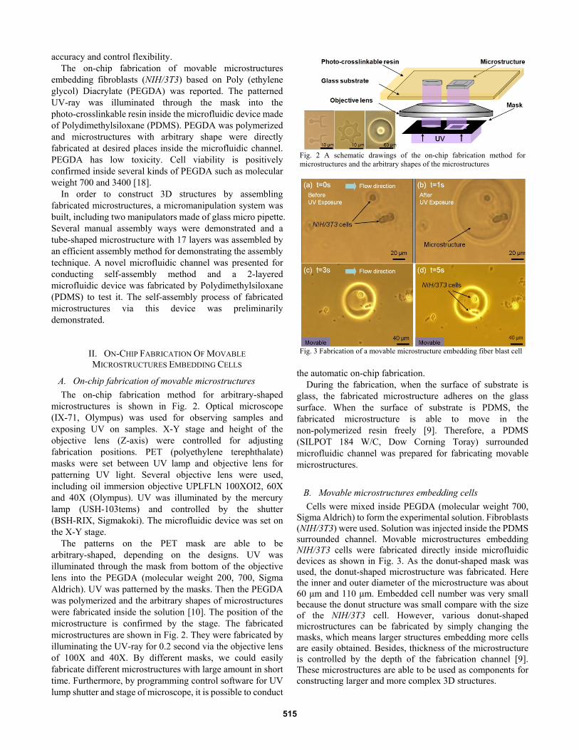
The on-chip fabrication method for arbitrary-shaped microstructures is shown in Fig. 2. Optical microscope (IX-71, Olympus) was used for observing samples and exposing UV on samples. X-Y stage and height of the objective lens (Z-axis) were controlled for adjusting fabrication positions. PET (polyethylene terephthalate) masks were set between UV lamp and objective lens for patterning UV light. Several objective lens were used, including oil immersion objective UPLFLN 100XOI2, 60X and 40X (Olympus). UV was illuminated by the mercury lamp (USH-103tems) and controlled by the shutter (BSH-RIX, Sigmakoki). The microfluidic device was set on the X-Y stage.
The patterns on the PET mask are able to be arbitrary-shaped, depending on the designs. UV was illuminated through the mask from bottom of the objective lens into the PEGDA (molecular weight 200, 700, Sigma Aldrich). UV was patterned by the masks. Then the PEGDA was polymerized and the arbitrary shapes of microstructures were fabricated inside the solution [10]. The position of the microstructure is confirmed by the stage. The fabricated microstructures are shown in Fig. 2. They were fabricated by illuminating the UV-ray for 0.2 second via the objective lens of 100X and 40X. By different masks, we could easily fabricate different microstructures with large amount in short time. Furthermore, by programming control software for UV lump shutter and stage of microscope, it is possible to conduct
the automatic on-chip fabrication. During the fabrication, when the surface of substrate is
glass, the fabricated microstructure adheres on the glass surface. When the surface of substrate is PDMS, the fabricated microstructure is able to move in the non-polymerized resin freely [9]. Therefore, a PDMS (SILPOT 184 W/C, Dow Corning Toray) surrounded microfluidic channel was prepared for fabricating movable microstructures.
B. Movable microstructures embedding cells
Cells were mixed inside PEGDA (molecular weight 700, Sigma Aldrich) to form the experimental solution. Fibroblasts (NIH/3T3) were used. Solution was injected inside the PDMS surrounded channel. Movable microstructures embedding NIH/3T3 cells were fabricated directly inside microfluidic devices as shown in Fig. 3. As the donut-shaped mask was used, the donut-shaped microstructure was fabricated. Here the inner and outer diameter of the microstructure was about 60 μm and 110 μm. Embedded cell number was very small because the donut structure was small compare with the size of the NIH/3T3 cell. However, various donut-shaped microstructures can be fabricated by simply changing the masks, which means larger structures embedding more cells are easily obtained. Besides, thickness of the microstructure is controlled by the depth of the fabrication channel [9]. These microstructures are able to be used as components for constructing larger and more complex 3D structures.
Fig. 2 A schematic drawings of the on-chip fabrication method for microstructures and the arbitrary shapes of the microstructures
Fig. 3 Fabrication of a movable microstructure embedding fiber blast cell
515

III. MANUAL ASSEMBLY FOR MULTI-LAYERED
MICROSTRUCTURES BASED ON MICROMANIPULATION
A. The experimental setup of the manual assembly system
In order to construct 3D structures by assembling the fabricated microstructures mentioned in Section 2-B, a micromanipulation system was built, including two manipulators made of glass micro pipette. As shown in Fig. 4, this is a manual assembly system with open chamber. The main manipulator was fixed on a mechanical stage with micro meter resolution. The sub manipulator was fixed with the dish in which the fabricated microstructures were collected. It is able to manipulate and assemble microstructures via these two manipulators.
The tips of the manipulators were made of glass micro pipettes of which the size was less than 10 μm. This kind of micro pipette is soft and hard to broken by bending. Microstructures were fabricated inside PDMS channel, then collected and transported to a culture dish, as shown in Fig 4. The inner and outer diameter of the microstructures was about 70 μm and 140 μm respectively. The thickness was about 40 μm. A microscope image of the completed manual micromanipulation system is shown in Fig. 5. The environment for manipulation is water.
B. Transportation assembly method
Based on the assembly system, several manual assembly ways were developed, including transportation assembly and non-transportation assembly methods, as shown in Fig. 6. The difference between them is the different functions of two manipulators and different final assembly places. The multi-layered tube-shaped structures were assembled for demonstrating these assembly techniques.
The assembly procedure of the transportation assembly is shown in Fig. 7(a). Firstly, a microstructure was picked up by main manipulator. Secondly, the main manipulator approached the sub manipulator. Thirdly, the microstructure was transported to the sub manipulator manually. Repeated the previous steps and finally the microstructures were assembled on the sub manipulator. For assembling one microstructure, the whole process took about 15 s. It is considered that the transportation assembly method is not efficient.
C. Non-transportation assembly method
Different with the transportation assembly, the assembly procedure of the non-transportation assembly is shown in Fig. 7(b).
Firstly, a microstructure was picked up by main manipulator. Secondly, the main manipulator approached the sub manipulator. Thirdly, the microstructure was pushed into the shaft part of main manipulator by sub manipulator manually. Repeated the previous steps and finally the microstructures were assembled on the main manipulator. The microstructures always remained on the main manipulator during the whole process. For assembling one microstructure, the whole process took about 10 s which was shorter than transportation assembly. However, it is still not so efficient for assembling large amount of microstructures in
short time. An assembled tube-shaped structure containing 3 layers is
shown in Fig. 8. This structure is not long enough and it takes time to construct it. Besides, long time of manipulation may cause the damage of cells which is not good for biological applications
D. An efficient assembly method based on non-transportation assembly
Based on the non-transportation assembly method, a novel and efficient assembly approach was developed. The basic idea is shown in Fig. 9. Only the main manipulator was used. By moving main manipulator downwards, the contact force F
Fig.4 The experimental setup of manual assembly system
Fig. 5 An micrograph of the manual micromanipulation system
Fig. 6 Two kinds of manul assembly methods
516
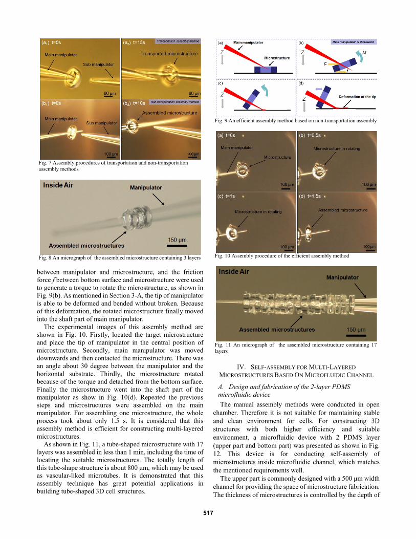
between manipulator and microstructure, and the friction force f between bottom surface and microstructure were used to generate a torque to rotate the microstructure, as shown in Fig. 9(b). As mentioned in Section 3-A, the tip of manipulator is able to be deformed and bended without broken. Because of this deformation, the rotated microstructure finally moved into the shaft part of main manipulator.
The experimental images of this assembly method are shown in Fig. 10. Firstly, located the target microstructure and place the tip of manipulator in the central position of microstructure. Secondly, main manipulator was moved downwards and then contacted the microstructure. There was an angle about 30 degree between the manipulator and the horizontal substrate. Thirdly, the microstructure rotated because of the torque and detached from the bottom surface. Finally the microstructure went into the shaft part of the manipulator as show in Fig. 10(d). Repeated the previous steps and microstructures were assembled on the main manipulator. For assembling one microstructure, the whole process took about only 1.5 s. It is considered that this assembly method is efficient for constructing multi-layered microstructures.
As shown in Fig. 11, a tube-shaped microstructure with 17 layers was assembled in less than 1 min, including the time of locating the suitable microstructures. The totally length of this tube-shape structure is about 800 μm, which may be used as vascular-liked microtubes. It is demonstrated that this assembly technique has great potential applications in building tube-shaped 3D cell structures.
IV. SELF-ASSEMBLY FOR MULTI-LAYERED
MICROSTRUCTURES BASED ON MICROFLUIDIC CHANNEL
A. Design and fabrication of the 2-layer PDMS microfluidic device
The manual assembly methods were conducted in open chamber. Therefore it is not suitable for maintaining stable and clean environment for cells. For constructing 3D structures with both higher efficiency and suitable environment, a microfluidic device with 2 PDMS layer (upper part and bottom part) was presented as shown in Fig. 12. This device is for conducting self-assembly of microstructures inside microfluidic channel, which matches the mentioned requirements well.
The upper part is commonly designed with a 500 μm width channel for providing the space of microstructure fabrication. The thickness of microstructures is controlled by the depth of
Fig. 7 Assembly procedures of transportation and non-transportation assembly methods
Fig. 8 An micrograph of the assembled microstructure containing 3 layers
Fig. 9 An efficient assembly method based on non-transportation assembly
Fig. 10 Assembly procedure of the efficient assembly method
Fig. 11 An micrograph of the assembled microstructure containing 17 layers
517

the channel [9], which is about 45 μm. There is a micro well inside the bottom part for assembling the fabricated movable microstructures and a micro groove for releasing solution but assembled microstructures. The depth of the well is 100 μm, and two types of length were prepared, which are 200 μm and 500 μm. The width of the groove is 30μm. The idea of self-assembly is shown as Fig. 12. The fabricated movable microstructures will flow with the solution and go into the micro well. Following the flow, the microstructures rotate 90 degrees inside the micro well and stop at the end of the micro well, because they are not able to go into the micro groove. The stopped microstructures will be assembled one by one. Finally, it will form a tube-shaped 3D structure with large amount of cells inside the micro well.
The fabrication method of this 2-layer microfluidic device is basically based on simply photolithography method. Here the two PDMS parts were bonded together and the channel was formed. The top views of the microfluidic channels are shown in Fig. 13. For testing the self-assembly process and constructing different length of tube-shaped structures, 2 types of channels were prepared. The width of the micro well and groove is about 140 μm and 30 μm respectively. And the depth of the upper channel and micro well is 45 μm and 100
μm respectively. Length of the micro well is 200 μm and 500 μm respectively for Fig. 13(a) and (b). All the parameters are acceptable.
B. Experimental results
Sample solution was injected to the inlet of the channel. Negative pressure was given from the outlet by a syringe pump. The on-chip fabrication and fluidic self-assembly were conducted inside the device. The experimental results of self-assembly are shown in Fig. 14. Movable microstructures were continually fabricated inside upper part channel and then moved with solution flow into the micro well of bottom part. The fabricated first microstructure approached to the micro well as shown in Fig. 9(a). It rotated 90 degrees and stopped at the end of the micro well by the micro grooves. Then the second one also approached to the micro well as shown in Fig. 9(b). The 3rd microstructure went into and assembled as shown in Fig. 9(c) and 9(d). After 8 seconds, 3 microstructures were assembled. The assembly efficiency may be influenced by the flow velocity, which means that the flow velocity is higher the assembly time can be shorter. The inner hollow of this tube-shaped structure is shown clearly in these micrographs. The great advantage of this method is that the whole process is done inside microfluidic channel without manual manipulation. Both the higher efficiency and the suitable environment are able to be obtained.
C. Discussion
Self-assembly of the microstructures was demonstrated. However, the experiment result is preliminarily, because of several unsolved problems. One is how to connect the
Fig. 14 Self-assembly result of microstructures in 200μm length micro well
Fig. 15 A tube-shaped microstructure with 6 layers collected inside water
Fig. 12 A schematic drawing of the 2-layer microfluidic device for self-assembly of movable microstructures
Fig. 13 Micrographs of top view of the microfluidic channels for self-assembly
518

assembled layers after assembly. The other one is how to remove the assembly structures from the manipulator or microfluidic channel.
For solving the first problem, a secondary UV exposure was conducted. After assembly, the solution in the channel was replaced to water, which is not photo-crosslinkable. Then secondary UV exposure was given to the whole assemble structure. Secondary UV exposure was totally 10s for the whole structure. Then the layers were firmly connected as one tube. For solving the second problem, sub manipulator was used to remove the connected structure from the main manipulator. In microfluidic case, we directly separated the 2 layers to open the channel and collected the assembled tube. A collected tube-shaped structure, with 6 layers firmly connected by secondary UV exposure, is shown in Fig. 15. It was assembly by the microfluidic channel.
However, the alignment of assembled layers was not good enough. There is displacement between some layers. The reason is that the diameter of microstructures is smaller than the width of micro well. It may be solved by modifying the size of the channel. Besides, there were no cells inside the used microstructures in assembly experiments. For next step, assembly of cell embedded structures should be conducted.
V. CONCLUSION
In this paper, we report a novel method of constructing multi-layered microstructures via micromanipulation system or microfluidic devices. The on-chip fabrication of movable microstructures embedding cells was reported. Two approaches for assembling these movable microstructures were presented. One was a manual assembly method based on micromanipulation system and the other one was a self-assembly method based on microfluidic channel. Several manual assembly ways were demonstrated and a tube-shaped microstructure with 17 layers was assembled by an efficient assembly method. A novel microfluidic channel was presented for conducting self-assembly method and a 2-layered microfluidic device was fabricated by PDMS. The self-assembly process of fabricated microstructures via this device was preliminarily demonstrated. The result shows great potential to be used in high-throughput cell 3D assembly for tissue engineering.
For the future works, an automatic assembly system based on the manual system is needed. The piezoceramic actuators and vision feedback can be applied. Microfluidic devices for self-assembly should be improved and the assembly of cell embedded microstructures should be conducted.
ACKNOWLEDGMENT
This work was partially supported by MEXT KAKENHI (Hyper Bio Assembler for 3D Cellular Systems (BioAssembler)) Grant Number 23106006 and COE for Education and Research of Micro-Nano Mechatronics of Nagoya University Global COE Program.
REFERENCES
[1] B. G. Chung, L. F. Kang, and A. Khademhosseini, “Micro- and nanoscale technologies for tissue engineering and drug discovery applications,” Expert Opinion on Drug Discovery, vol. 2, no. 12, pp. 1653-1668, Dec, 2007
[2] E. J. Suuronen, H. Sheardown, K. D. Newman et al., "Building In Vitro Models of Organs," International Review of Cytology, W. J. Kwang, ed., pp. 137-173: Academic Press, 2005
[3] R. Langer, and J. P. Vacanti, “Tissue Engineering,” Science, vol. 260, no. 5110, pp. 920-926, May, 1993
[4] S. R. Khetani, and S. N. Bhatia, “Engineering tissues for in vitro applications,” Current Opinion in Biotechnology, vol. 17, no. 5, pp. 524-531, 2006
[5] H. Kaji, G. Camci-Unal, R. Langer et al., “Engineering systems for the generation of patterned co-cultures for controlling cell-cell interactions,” Biochimica Et Biophysica Acta-General Subjects, vol. 1810, no. 3, pp. 239-250, Mar, 2011
[6] H. Tsutsui, et al., "Efficient Dielectrophoretic Patterning of Embryonic Stem Cells in Energy Landscapes Defined by Hydrogel Geometries," Annals of Biomedical Engineering, vol. 38, pp. 3777-3788, Dec 2010.
[7] A. Tixier-Mita, J. Jun, S. Ostrovidov, M. Chiral, M. Frenea, B Le Pioufle, H. Fujita, "A silicon micro-system for parallel gene transfection into arrayed cells," Proceedings of the uTAS 2004 Symposium, The Royal Society of Chemistry, pp. 180-1822004
[8] D. Di Carlo, N. Aghdam, and L. P. Lee, "Single-cell enzyme concentrations, kinetics, and inhibition analysis using high-density hydrodynamic cell isolation arrays," Analytical Chemistry, vol. 78, no. 14, pp. 4925-4930, Jul, 2006
[9] D. Dendukuri, D. C. Pregibon, J. Collins et al., “Continuous-flow lithography for high-throughput microparticle synthesis,” Nature Materials, vol. 5, no. 5, pp. 365-369, May, 2006
[10] T. Yue, M. Nakajima, H. Tajima and T. Fukuda. “Fabrication of Microstructures Embedding Controllable Particles Inside Dielectrophoretic Microfluidic Devices”, International Journal of Advanced Robotic Systems, Vol.10. Published online, 15 Feb., 2013,
[11] Y. T. Matsunaga, Y. Morimoto, and S. Takeuchi, “Molding Cell Beads for Rapid Construction of Macroscopic 3D Tissue Architecture,” Advanced Materials, vol. 23, no. 12, pp. H90-H94, 2011
[12] M. Yamada, R. Utoh, K. Ohashi et al., “Controlled formation of heterotypic hepatic micro-organoids in anisotropic hydrogel microfibers for long-term preservation of liver-specific functions,” Biomaterials, vol. 33, no. 33, pp. 8304-8315, 2012
[13] P. Panda, S. Ali, E. Lo, B.G. Chung, T.A. Hatton, A. Khademhosseini, and P.S. Doyle, “Stop-flow lithography to generate cell-laden microgel particles,” Lab Chip, vol. 8, (no. 7), pp. 1056-1061, 2008
[14] Y. Du, M. Ghodousi, H. Qi et al., “Sequential assembly of cell-laden hydrogel constructs to engineer vascular-like microchannels,” Biotechnology and Bioengineering, vol. 108, pp. 1693-1703, 2011
[15] G.M. Whitesides and B. Grzybowski, "Self-assembly at all scales," Science, vol. 295, (no. 5564), pp. 2418-2421, 2002
[16] W. Zheng and H.O. Jacobs, "Fabrication of multicomponent microsystems by directed three-dimensional self-assembly," Advanced Functional Materials, vol. 15, (no. 5), pp. 732-738, 2005
[17] S.E. Chung, Y. Jung, and S. Kwon, "Three-Dimensional Fluidic Self-Assembly by Axis Translation of Two-Dimensionally Fabricated Microcomponents in Railed Microfluidics," Small, vol. 7, (no. 6), pp. 796-803, 2011
[18] V. Chan, P. Zorlutuna, J.H. Jeong, H. Kong, and R. Bashir, “Three-dimensional photopatterning of hydrogels using stereolithography for long-term cell encapsulation,” Lab Chip, vol. 10, (no. 16), pp. 2062-2070, 2010
519