fa-m3 sequence cpu instruction manual - functions (for ...the functions of the f3sp28, f3sp38,...
TRANSCRIPT

InstructionManual
Yokogawa Electric Corporation
IM 34M6P12-02E
Sequence CPU InstructionManual - Functions(for F3SP21, F3SP25 andF3SP35)
IM 34M6P12-02E3rd Edition

Blank Page

i
IM 34M6P12-02EMedia No. IM 34M6P12-02E (CD) 3rd Edition : Oct 2001 (AR)All Rights Reserved Copyright © 1998, Yokogawa Electric Corporation
3rd Edition : Oct 1, 2001-00
Applicable Product:
Range-free Multi-controller FA-M3
• Model Name: F3SP21, F3SP25, F3SP35, F3SP05-0P, F3SP08-0P
• Name: Sequence CPU Modules
The document number and document code for this manual are as follows:
Refer to the document number in all communications; also refer to the document number orthe document model code when purchasing copies of this manual.
• Document No.: IM34M6P12-02E
• Document Code: DOCIM
CAUTION
The functions of the F3SP28, F3SP38, F3SP53 and F3SP58 sequence CPU modulesare not explained in this manual. For information on these functions, refer to SequenceCPU Instruction Manual - Functions (for F3SP28, F3SP38, F3SP53 and F3SP58)(IM34M6P13-01E).
ii
IM 34M6P12-02E
Important
About This Manual- This Manual should be passed on to the end user.
- Before using the controller, read this manual thoroughly to have a clear understandingof the controller.
- This manual explains the functions of this product, but there is no guarantee that theywill suit the particular purpose of the user.
- Under absolutely no circumstances may the contents of this manual be transcribed orcopied, in part or in whole, without permission.
- The contents of this manual are subject to change without prior notice.
- Every effort has been made to ensure accuracy in the preparation of this manual.However, should any errors or omissions come to the attention of the user, pleasecontact the nearest Yokogawa Electric representative or sales office.
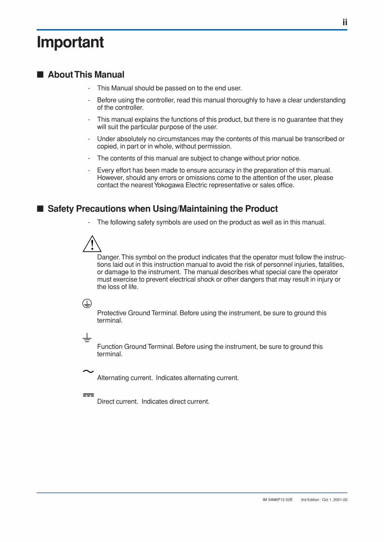
Safety Precautions when Using/Maintaining the Product- The following safety symbols are used on the product as well as in this manual.
Danger. This symbol on the product indicates that the operator must follow the instruc-tions laid out in this instruction manual to avoid the risk of personnel injuries, fatalities,or damage to the instrument. The manual describes what special care the operatormust exercise to prevent electrical shock or other dangers that may result in injury orthe loss of life.
Protective Ground Terminal. Before using the instrument, be sure to ground thisterminal.
Function Ground Terminal. Before using the instrument, be sure to ground thisterminal.
Alternating current. Indicates alternating current.
Direct current. Indicates direct current.
3rd Edition : Oct 1, 2001-00

iii
IM 34M6P12-02E
The following symbols are used only in the instruction manual.
WARNINGIndicates a “Warning”.Draws attention to information essential to prevent hardware damage, softwaredamage or system failure.
CAUTIONIndicates a “Caution”
Draws attention to information essential to the understanding of operation and func-tions.
TIP
Indicates a “TIP”Gives information that complements the present topic.
SEE ALSO
Indicates a “SEE ALSO” reference.Identifies a source to which to refer.
- For the protection and safe use of the product and the system controlled by it, be sureto follow the instructions and precautions on safety stated in this manual wheneverhandling the product. Take special note that if you handle the product in a mannerother than prescribed in these instructions, the protection feature of the product maybe damaged or impaired. In such cases, Yokogawa cannot guarantee the quality,performance, function and safety of the product.
- When installing protection and/or safety circuits such as lightning protection devicesand equipment for the product and control system as well as designing or installingseparate protection and/or safety circuits for fool-proof design and fail-safe design ofprocesses and lines using the product and the system controlled by it, the user shouldimplement it using devices and equipment, additional to this product.
- If component parts or consumable are to be replaced, be sure to use parts specifiedby the company.
- This product is not designed or manufactured to be used in critical applications whichdirectly affect or threaten human lives and safety - such as nuclear powerequipment, devices using radioactivity, railway facilities, aviation equipment, air navigation facilities, aviation facilities or medical equipment. If so used, it is the user’sresponsibility to include in the system additional equipment and devices that ensurepersonnel safety.
- Do not attempt to modify the product.
Exemption from Responsibility- Yokogawa Electric Corporation (hereinafter simply referred to as Yokogawa Electric)
makes no warranties regarding the product except those stated in the WARRANTYthat is provided separately.
- Yokogawa Electric assumes no liability to any party for any loss or damage, direct orindirect, caused by the user or any unpredictable defect of the product.
3rd Edition : Oct 1, 2001-00

iv
IM 34M6P12-02E
Software Supplied by the Company- Yokogawa Electric makes no other warranties expressed or implied except as pro-
vided in its warranty clause for software supplied by the company.
- Use the software with one computer only. You must purchase another copy of thesoftware for use with each additional computer.
- Copying the software for any purposes other than backup is strictly prohibited.
- Store the original media, such as floppy disks, that contain the software in a safeplace.
- Reverse engineering, such as decompiling of the software, is strictly prohibited.
- No portion of the software supplied by Yokogawa Electric may be transferred, ex-changed, or sublet or leased for use by any third party without prior permission byYokogawa Electric.
3rd Edition : Oct 1, 2001-00

v
IM 34M6P12-02E
General Requirements for Using the FA-M3 Controller
Avoid installing the FA-M3 controller in the following locations:
- Where the instrument will be exposed to direct sunlight, or where the operating tem-perature exceeds the range 0°C to 55°C (0°F to 131°F).
- Where the relative humidity is outside the range 10 to 90%, or where sudden tempera-ture changes may occur and cause condensation.
- Where corrosive or flammable gases are present.
- Where the instrument will be exposed to direct mechanical vibration or shock.
- Where the instrument may be exposed to extreme levels of radioactivity.
Use the correct types of wire for external wiring:
- Use copper wire with temperature ratings greater than 75°C.
Securely tighten screws:
- Securely tighten module mounting screws and terminal screws to avoid problemssuch as faulty operation.
- Tighten terminal block screws with the correct tightening torque as given in thismanual.
Securely lock connecting cables:
- Securely lock the connectors of cables, and check them thoroughly before turning onthe power.
Interlock with emergency-stop circuitry using external relays:
- Equipment incorporating the FA-M3 controller must be furnished with emergency-stopcircuitry that uses external relays. This circuitry should be set up to interlock correctlywith controller status (stop/run).
Ground for low impedance:
- For safety reasons, connect the [FG] grounding terminal to a Japanese IndustrialStandards (JIS) Class D Ground*1 (Japanese Industrial Standards (JIS) Class 3Ground). For compliance to CE Marking, use cables such as twisted cables which canensure low impedance even at high frequencies for grounding.
*1 Japanese Industrial Standards (JIS) Class D Ground means grounding resistance of 100Ω max.
Configure and route cables with noise control considerations:
- Perform installation and wiring that segregates system parts that may likely becomenoise sources and system parts that are susceptible to noise. Segregation can beachieved by measures such as segregating by distance, installing a filter orsegregating the grounding system.
Configure for CE Marking Conformance:
- For compliance to CE Marking, perform installation and cable routing according tothe description on compliance to CE Marking in the “Hardware Manual”(IM34M6C11-01E).
3rd Edition : Oct 1, 2001-00
vi
IM 34M6P12-02E 3rd Edition : Oct 1, 2001-00
Keep spare parts on hand:
- Stock up on maintenance parts including spare modules, in advance.
Discharge static electricity before operating the system:
- Because static charge can accumulate in dry conditions, first touch grounded metal todischarge any static electricity before touching the system.
Never use solvents such as paint thinner for cleaning:
- Gently clean the surfaces of the FA-M3 controller with a cloth that has been soaked inwater or a neutral detergent and wringed.
- Do not use volatile solvents such as benzine or paint thinner or chemicals for cleaning,as they may cause deformity, discoloration, or malfunctioning.
Avoid storing the FA-M3 controller in places with high temperature orhumidity:
- Since the CPU module has a built-in battery, avoid storage in places with hightemperature or humidity.
- Since the service life of the battery is drastically reduced by exposure to hightemperatures, take special care (storage temperature should be from -20°C to 75°C).
- There is a built-in lithium battery in a CPU module and temperature control modulewhich serves as backup power supply for programs, device information andconfiguration information. The service life of this battery is more than 10 years instandby mode at room temperature. Take note that the service life of the batterymay be shortened when installed or stored at locations of extreme low or hightemperatures. Therefore, we recommend that modules with built-in batteries be storedat room temperature.
Always turn off the power before installing or removing modules:
- Failing to turn off the power supply when installing or removing modules, may result indamage.
Do not touch components in the module:
- In some modules you can remove the right-side cover and install ROM packs orchange switch settings. While doing this, do not touch any components on theprinted-circuit board, otherwise components may be damaged and modules may failto work.

vii
IM 34M6P12-02E
Waste Electrical and Electronic EquipmentWaste Electrical and Electronic Equipment (WEEE), Directive 2002/96/EC(This directive is only valid in the EU.)
This product complies with the WEEE Directive (2002/96/EC) marking requirement.
The following marking indicates that you must not discard this electrical/electronic productin domestic household waste.
Product Category
With reference to the equipment types in the WEEE directive Annex 1, this product isclassified as a “Monitoring and Control instrumentation” product.
Do not dispose in domestic household waste.
When disposing products in the EU, contact your local Yokogawa Europe B. V. office.
3rd Edition : Oct 1, 2001-00
viii
IM 34M6P12-02E 3rd Edition : Oct 1, 2001-00
Introduction
Overview of the ManualThis manual describes the sequencing functions of the F3SP21, F3SP25 and F3SP35sequence CPU modules designed for use with the FA-M3 Range-free Multi-controllerand the F3SP05-0P and F3SP08-0P sequence CPU module designed for use withsmall-scale controllers.
Structure of the ManualThis manual consists of three parts:
Part A: Standard Version
The main part of this manual explains the functions of the sequence CPU modules, exclud-ing the F3SP05-0P and the F3SP08-0P, for use with the FA-M3 system.
Part B: F3SP05-0P Sequence CPU for FA-M3 Value
The second part of this manual explains the functions specific to the F3SP05-0P sequenceCPU module.
Part C: F3SP08-0P Sequence CPU for FA-M3 Value II
The third part of this manual explains the functions specific to the F3SP08-0P sequenceCPU module.
Chapters corresponding to Chapters A3 to A8 of Part A “Standard Version” are not includedin Part B and Part C. When using the F3SP05-0P sequence CPU and the F3SP08-0P,assume the F3SP05-0P and the F3SP08-0P to be Model F3SP21 and refer to the relevantparagraphs of these chapters where the F3SP21 is discussed.
ix
IM 34M6P12-02E 3rd Edition : Oct 1, 2001-00
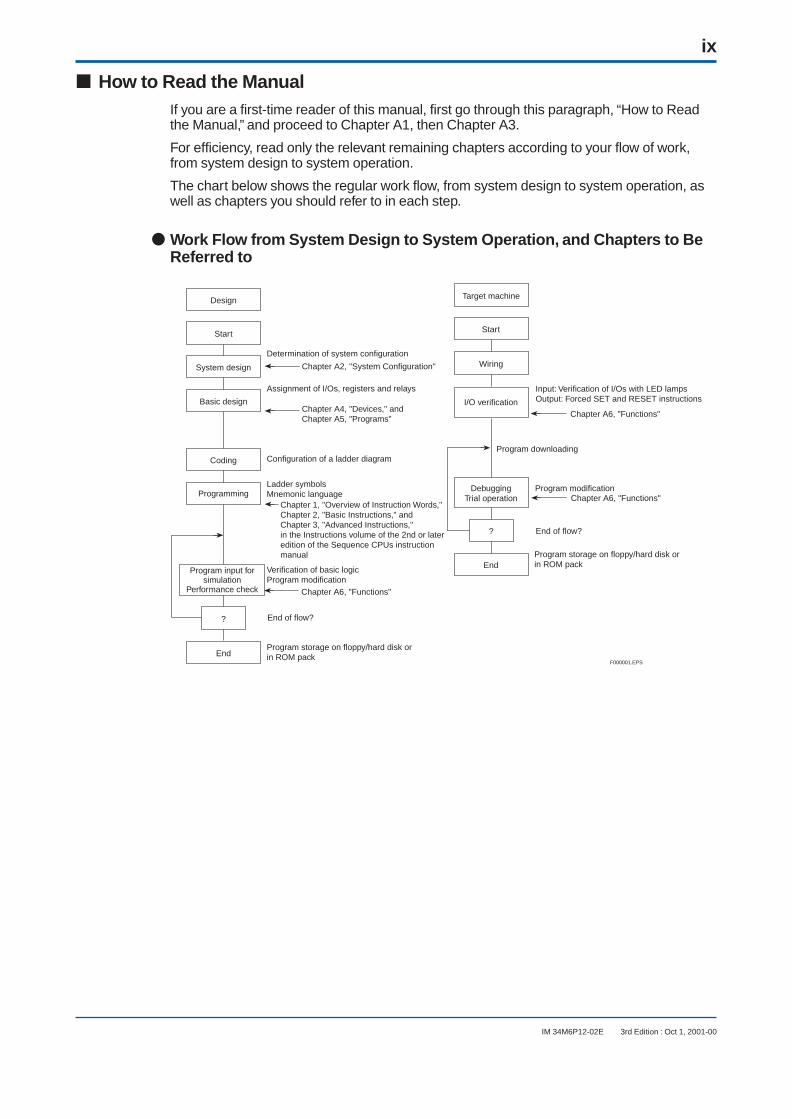
How to Read the ManualIf you are a first-time reader of this manual, first go through this paragraph, “How to Readthe Manual,” and proceed to Chapter A1, then Chapter A3.
For efficiency, read only the relevant remaining chapters according to your flow of work,from system design to system operation.
The chart below shows the regular work flow, from system design to system operation, aswell as chapters you should refer to in each step.
Work Flow from System Design to System Operation, and Chapters to BeReferred to
Determination of system configuration
System design
Design
Basic design
Programming
Program downloadingCoding
Program input for simulation
Performance check
I/O verification
Input: Verification of I/Os with LED lampsOutput: Forced SET and RESET instructions
DebuggingTrial operation
End
Start
Assignment of I/Os, registers and relays
Configuration of a ladder diagram
Ladder symbolsMnemonic language
Verification of basic logicProgram modification
Program modificationChapter A6, "Functions"
Chapter A6, "Functions"
Chapter A6, "Functions"
Chapter A2, "System Configuration"
Chapter A4, "Devices," andChapter A5, "Programs"
Chapter 1, "Overview of Instruction Words,"Chapter 2, "Basic Instructions," andChapter 3, "Advanced Instructions,"in the Instructions volume of the 2nd or later edition of the Sequence CPUs instruction manual
Program storage on floppy/hard disk or in ROM pack
End of flow?
Program storage on floppy/hard disk or in ROM pack
End of flow?
?
End
Start
?
Wiring
Target machine
F000001.EPS
x
IM 34M6P12-02E 3rd Edition : Oct 1, 2001-00
Notational Conventions
Symbol Marks Used in This Manual
The following symbol marks are used in this manual.
F3SP21F3SP25F3SP35
: Refers to a topic that applies to the F3SP21, F3SP25 and F3SP35.
F3SP25F3SP35 : Refers to a topic that applies to the F3SP25 and F3SP35.
In the absence of any symbol mark, it should be assumed that the topic applies to theF3SP21, F3SP25 and F3SP35.
Other Instruction Manuals
CAUTION
The functions of the F3SP28, F3SP38, F3SP53 and F3SP58 sequence CPU modules arenot explained in this manual. For information on these functions, refer to the instructionmanual (IM34M6P13-01E), Sequence CPU Instruction Manual - Functions (for F3SP28,F3SP38, F3SP53 and F3SP58).
Be sure to read each of the following manuals, in addition to this manual.
For information on the instructions used with sequence CPUs, refer to:
• Sequence CPU Instruction Manual - Instructions (IM34M6P12-03E).
For information on the specifications*, configuration, installation, wiring,trial operation, maintenance and inspection of the FA-M3, as well as infor-mation on the system-wide limitation of module installation, refer to:
• Hardware Manual (IM34M6C11-01E) .
* For information on the specifications of products other than the power supply module, base module, I/O module, cable and terminal block unit, refer to their respective instruction manuals.
When creating programs using ladder language, refer to:
• FA-M3 Programming Tool WideField Instruction Manual (IM34M6Q14-01E); and
• FA-M3 Programming Tool WideField - Instruction Manual-Applications(IM34M6Q14-02E).
- or -
• Ladder Diagram Support Program M3 Instruction Manual (IM34M6Q13-01E).
Read the following instruction manuals, as necessary.

xi
IM 34M6P12-02E
For information on the functions of fiber-optic FA-bus modules, refer to:
• Fiber-optic FA-bus Module and Fiber-optic FA-bus Type 2 Module Instruction Manual(IM34M6H45-01E) .
For information on the functions of FA link H and fiber-optic FA link Hmodules, refer to:
• FA Link H Module F3LP02-0N Fiber-optic FA Link H Module F3LP12-0N(IM34M6H43-01E).
For information on the functions of F3SP28, F3SP38, F3SP53 and F3SP58sequence CPU modules, refer to:
• Sequence CPU Instruction Manual - Functions (for F3SP28, F3SP38, F3SP53 andF3SP58) (IM34M6P13-01E).
For information on the functions of BASIC CPU modules, refer to:
• BASIC CPU Modules and YM-BASIC/FA Programming Language Instruction Manual(IM34M6Q22-01E).
For information on the functions of the F3FP36 sequence CPU module,refer to:
• Sequence CPU - Functions Instruction Manual (for F3FP36) (IM34M6P22-01E).
3rd Edition : Oct 1, 2001-00
xii
IM 34M6P12-02E
Copyright and Trademarks
CopyrightsCopyrights of the programs and online manual included in this CD-ROM belong toYokogawa Electric Corporation.
This online manual may be printed but PDF security settings have been made to preventalteration of its contents.
This online manual may only be printed and used for the sole purpose of operating thisproduct. When using a printed copy of the online manual, pay attention to possibleinconsistencies with the latest version of the online manual. Ensure that the editionagrees with the lateat CE-ROM version.
Copying, passing selling or distribution (including transferring over computer networks)of the contents of the online manual, in part or in whole, to any third party, is strictlyprohibited. Registering or recording onto videotapes and other media is also prohibitedwithout expressed permission of Yokogawa Electric Corporation.
TrademarksThe trade names and company names referred to in this manual are either trademarksor registered trademarks of their respective companies.
3rd Edition : Oct 1, 2001-00

Toc-1
IM 34M6P12-02E
CONTENTS
3rd Edition : Oct 1, 2001-00
IM 34M6P12-02E 3rd Edition
Sequence CPU Instruction Manual - Functions(for F3SP21, F3SP25 and F3SP35)
Applicable Product ............................................................................................... i
Important ...............................................................................................................ii
Introduction........................................................................................................viii
Copyrights and Trademarks ...............................................................................xii
PART A for F3SP21, F3SP25 and F3SP35A1. Specification and Basic Configuration ................................................ A1-1
A1.1 Overview........................................................................................................ A1-1
A1.1.1 CPU Modules ................................................................................. A1-1
A1.2 Specification ................................................................................................. A1-3
A1.2.1 Table of Performance Data .............................................................. A1-3
A1.2.2 Device List ...................................................................................... A1-5
A1.2.3 Configuration .................................................................................. A1-7
A1.2.4 Components and Their Functions ................................................. A1-12
A1.2.5 External Dimensions ..................................................................... A1-13
A1.3 Basic configuration .................................................................................... A1-14
A1.3.1 Unit ............................................................................................... A1-14
A1.3.2 Slot Number ................................................................................. A1-15
A1.3.3 I/O Relay Number ......................................................................... A1-17
A2. System Configuration .......................................................................... A2-1A2.1 Basic System Configuration ........................................................................ A2-1
A2.2 Multi-CPU System Configuration ................................................................. A2-1
A2.2.1 Multi-CPU System Configuration .................................................... A2-1
A2.2.2 Handling I/O Modules in Multi-CPU System .................................... A2-2
A2.3 Extended System Configuration .................................................................. A2-3
A2.3.1 Remote I/O System ........................................................................ A2-3
A2.3.2 Personal Computer Link System ..................................................... A2-3
A2.3.3 FA Link System ............................................................................... A2-4
A2.4 Programming Tools ....................................................................................... A2-5
A2.4.1 WideField ....................................................................................... A2-5
A2.4.2 Ladder Diagram Support Program M3 ............................................ A2-7

Toc-2
IM 34M6P12-02E 3rd Edition : Oct 1, 2001-00
A3. Basic CPU Operations .......................................................................... A3-1A3.1 Operation Modes of CPU .............................................................................. A3-1
A3.2 Operation at Power-on/off ............................................................................ A3-2
A3.2.1 Operation at Power-on .................................................................... A3-2
A3.2.2 Operation at Power-off .................................................................... A3-2
A3.3 Operation in Case of Momentary or Complete Power Failure .................... A3-3
A3.3.1 Operation in Case of Momentary Power Failure .............................. A3-3
A3.3.2 Specifying the Momentary Power Failure Detection Mode ............... A3-3
A3.3.3 Operation in Case of Complete Power Failure ................................. A3-4
A3.3.4 Specifying the Range of Devices to Be Latched in Case of
Complete Power Failure .................................................................. A3-4
A3.4 Computation Method .................................................................................... A3-6
A3.5 Method of I/O Processing ............................................................................. A3-8
A3.5.1 Method of I/O Processing ............................................................... A3-8
A3.5.2 Response Delay ............................................................................. A3-9
A3.5.3 I/O Processing in Multi-CPU System ............................................... A3-9
A3.6 Method of Executing Commands from the Programming Tool ................ A3-10
A3.6.1 Tool Service .................................................................................. A3-10
A3.7 Method of Executing Commands through Personal Computer Link ....... A3-11
A3.7.1 Link Service .................................................................................. A3-11
A3.8 Method of CPU-to-CPU Data Communication ........................................... A3-12
A3.8.1 Shared Refreshing ........................................................................ A3-12
A3.8.2 CPU Service ................................................................................. A3-14
A3.9 Method of Link Data Updating .................................................................... A3-15
A3.9.1 Link Refreshing ............................................................................. A3-15
A3.10 Method of Interrupt Processing ................................................................. A3-17
A3.10.1 Interrupt Processing ..................................................................... A3-17
A3.10.2 Interrupt Processing Control ......................................................... A3-18
A4. Devices.................................................................................................. A4-1A4.1 I/O Relays (X/Y).............................................................................................. A4-1
A4.1.1 Input Relays (X) .............................................................................. A4-1
A4.1.2 Output Relays (Y) ........................................................................... A4-2
A4.1.3 Allocation of I/O Addresses ............................................................. A4-2
A4.1.4 Configuring DI/O Modules............................................................... A4-3
A4.2 Internal Relays (I), Shared Relays (E) and Extended Shared Relays (E) .... A4-5
A4.2.1 Internal Relays (I) ........................................................................... A4-5
A4.2.2 Shared Relays (E) and Extended Shared Relays (E) ...................... A4-6
A4.2.3 Configuring Internal Relays (I), Shared Relays (E) and Extended SharedRelays (E) ....................................................................................... A4-9
Toc-3
IM 34M6P12-02E
A4.3 Link Relays (L) and Link Registers (W) ...................................................... A4-11
A4.3.1 Link Relays (L) .............................................................................. A4-11
A4.3.2 Link Registers (W) ........................................................................ A4-16
A4.3.3 Configuring Link Relays (L) and Registers (W) .............................. A4-21
A4.4 Special Relays (M) ....................................................................................... A4-22
A4.4.1 Block Start Status ......................................................................... A4-22
A4.4.2 Utility Relays ................................................................................. A4-23
A4.4.3 Sequence Operation and Mode Status Relays .............................. A4-24
A4.4.4 Self-diagnosis Status Relays ........................................................ A4-25
A4.4.5 FA Link Module Status Relays ...................................................... A4-26
A4.5 Timers (T) .................................................................................................... A4-27
A4.5.1 1-ms, 10-ms, and 100-ms Timers .................................................. A4-27
A4.5.2 100-ms Continuous Timer ............................................................. A4-28
A4.5.3 Selecting Timers ........................................................................... A4-29
A4.6 Counters (C) ................................................................................................ A4-30
A4.6.1 Selecting Counters ....................................................................... A4-31
A4.7 Data Registers (D), Shared Registers (R),
and Extended Shared Registers (R) ........................................................... A4-32
A4.7.1 Data Registers (D) ........................................................................ A4-32
A4.7.2 Shared Registers (R) and Extended Shared Registers (R) ............ A4-33
A4.7.3 Configuring Data Registers (D), Shared Registers (R)
and Extended Shared Registers (R) ............................................. A4-36
A4.7.4 Setting Initial Data ......................................................................... A4-38
A4.8 Special Registers (Z) ................................................................................... A4-39
A4.8.1 Sequence Operation Status Registers .......................................... A4-39
A4.8.2 Self-diagnosis Status Registers .................................................... A4-40
A4.8.3 Utility Registers ............................................................................. A4-42
A4.8.4 FA Link Module Status Registers .................................................. A4-43
A4.8.5 CPU Module Status Registers ...................................................... A4-44
A4.9 Index Registers (V) ...................................................................................... A4-45
A4.10 File Registers (B) (F3SP25, F3SP35) .......................................................... A4-46
A5. Programs .............................................................................................. A5-1A5.1 Programming Language ............................................................................... A5-1
A5.1.1 Structured Ladder Language .......................................................... A5-1
A5.1.2 Mnemonic Language ...................................................................... A5-2
A5.2 Program Types and Configuration ............................................................... A5-3
A5.2.1 Blocks and Executable Programs.................................................... A5-3
A5.2.2 Programs Composing an Executable Program................................ A5-5
A5.3 Program Memory .......................................................................................... A5-9
3rd Edition : Oct 1, 2001-00
Toc-4
IM 34M6P12-02E
A6. Functions .............................................................................................. A6-1A6.1 Function List ................................................................................................. A6-1
A6.2 Operation Setup Function ............................................................................ A6-3
A6.3 Constant Scan ............................................................................................... A6-5
A6.3.1 Setting the Constant Scan Time ...................................................... A6-5
A6.4 Executing All Blocks/Specified Blocks ........................................................ A6-6
A6.4.1 Executing All Blocks ........................................................................ A6-6
A6.4.2 Executing Specified Blocks ............................................................. A6-7
A6.4.3 Operation when Specified Blocks Are Enabled ............................... A6-8
A6.4.4 Operation when Specified Blocks Are Disabled ............................. A6-10
A6.4.5 Operation When Specified Blocks Are Executed ........................... A6-11
A6.5 Debugging Functions ................................................................................. A6-13
A6.5.1 Step Operation ............................................................................. A6-13
A6.5.2 Scan Operation ............................................................................. A6-14
A6.5.3 Partial Operation ........................................................................... A6-15
A6.5.4 Forced SET/RESET.................................................................... A6-15
A6.5.5 Changing Setpoints, Current Values and Data Values ................. A6-16
A6.5.6 Stopping Refreshing ..................................................................... A6-16
A6.6 Protecting Programs................................................................................... A6-17
A6.6.1 Executable Program Protection ..................................................... A6-17
A6.6.2 Block Protection ............................................................................ A6-18
A6.7 Online Editing ............................................................................................. A6-19
A6.8 Making Programs Resident Using ROM Writer Functions ........................ A6-20
A6.8.1 Making Programs Resident in ROM .............................................. A6-20
A6.8.2 Setting Devices’ Current Values to Be Made Resident in ROM ...... A6-23
A6.8.3 ROM Writer Functions and ROM Writer Mode ............................... A6-24
A6.9 Exclusive Access Right .............................................................................. A6-26
A6.10 Sampling Trace Function ............................................................................ A6-27
A6.11 Personal Computer Link Function ............................................................. A6-31
A6.11.1 System Configuration ................................................................... A6-32
A6.11.2 Differences from Personal Computer Link Module ........................ A6-33
A6.11.3 Specification of Personal Computer Link Function ........................ A6-34
A6.11.4 Setting Up the Personal Computer Link Function .......................... A6-35
A6.11.5 Communication Procedure ........................................................... A6-37
A6.11.6 Commands and Responses ......................................................... A6-39
A6.12 Device Management Function .................................................................... A6-47
A6.13 Macro Instructions ...................................................................................... A6-48
A6.13.1 What Are Macro Instructions? ....................................................... A6-48
A6.13.2 Specification of Macro Instructions................................................ A6-50
A6.13.3 Devices Dedicated to Macro Instructions ...................................... A6-51
3rd Edition : Oct 1, 2001-00
Toc-5
IM 34M6P12-02E 3rd Edition : Oct 1, 2001-00
A6.13.4 Nesting Macro Instructions ........................................................... A6-53
A6.13.5 Handling Macro Instruction Errors ................................................. A6-55
A6.13.6 Protecting Macro Instructions ....................................................... A6-56
A6.13.7 Debugging Operation .................................................................... A6-56
A6.14 User Log Management Function ................................................................ A6-57
A7. I/O Response Time Based on Scan Time ............................................. A7-1A7.1 Scan Time ...................................................................................................... A7-1
A7.2 Setting Scan Time Monitoring Time ............................................................. A7-2
A7.3 Examples of Calculating the Scan Time ...................................................... A7-3
A7.4 Examples of Calculating the I/O Response Time ........................................ A7-5
A7.5 Instruction Execution Time........................................................................... A7-6
A8. RAS Features ........................................................................................ A8-1A8.1 Self-diagnosis ............................................................................................... A8-1
A8.1.1 Setting Operation Mode in Case of Failure
and External Output Mode in Case of Sequence Stop .................... A8-9
A8.2 Recovering Normal Operation after Correcting Moderate/
Minor Failures ............................................................................................. A8-10
PART B for CPU module designed for the FA-M3 Valuesystem (F3SP05-0P)
B1. Specification and Basic Configuration ................................................ B1-1B1.1 Overview........................................................................................................ B1-1
B1.2 Specification ................................................................................................. B1-3
B1.2.1 Performance Data ........................................................................... B1-3
B1.2.2 Device List ...................................................................................... B1-5
B1.2.3 Configuration .................................................................................. B1-6
B1.2.4 Components and Their Functions ................................................... B1-8
B1.2.5 External Dimensions ....................................................................... B1-9
B1.3 Basic Configuration .................................................................................... B1-10
B1.3.1 Units ............................................................................................. B1-10
B1.3.2 Slot Number ................................................................................. B1-11
B1.3.3 I/O Relay Number ......................................................................... B1-11
B2. System Configuration .......................................................................... B2-1B2.1 Basic System Configuration ........................................................................ B2-1
B2.2 Extended System Configuration .................................................................. B2-2
B2.2.1 Remote I/O System ........................................................................ B2-2
B2.2.2 Personal Computer Link System ..................................................... B2-3
B2.2.3 FA Link System ............................................................................... B2-3
B2.3 Programming Tools ....................................................................................... B2-4
B2.3.1 WideField ....................................................................................... B2-4
B2.3.2 Ladder Diagram Support Program M3 ............................................ B2-6
Toc-6
IM 34M6P12-02E
PART C for CPU module designed for the FA-M3 Value IIsystem (F3SP08-0P)
C1. Specification and Basic Configuration ................................................ C1-1C1.1 Overview........................................................................................................ C1-1
C1.2 Specification ................................................................................................. C1-3
C1.2.1 Performance Data ........................................................................... C1-3
C1.2.2 Device List ...................................................................................... C1-5
C1.2.3 Configuration .................................................................................. C1-6
C1.2.4 Components and Their Functions ................................................... C1-8
C1.2.5 External Dimensions ....................................................................... C1-9
C1.3 Basic Configuration .................................................................................... C1-10
C1.3.1 Units ............................................................................................. C1-10
C1.3.2 Slot Number ................................................................................. C1-11
C1.3.3 I/O Relay Number ......................................................................... C1-11
C2. System Configuration .......................................................................... C2-1C2.1 Basic System Configuration ........................................................................ C2-1
C2.2 Extended System Configuration .................................................................. C2-2
C2.2.1 Remote I/O System ........................................................................ C2-2
C2.2.2 Personal Computer Link System ..................................................... C2-3
C2.2.3 FA Link System ............................................................................... C2-3
C2.3 Programming Tools ....................................................................................... C2-4
C2.3.1 WideField ....................................................................................... C2-4
Appendix 1. Special Relays (M) ..............................................................App.1-1Appendix 1.1 Block Start Status ......................................................................... App.1-1
Appendix 1.2 Utility Relays .................................................................................. App.1-2
Appendix 1.3 Sequence Operation and Mode Status Relays ............................ App.1-4
Appendix 1.4 Self-diagnosis Status Relays ........................................................ App.1-5
Appendix 1.5 FA Link Module Status Relays ...................................................... App.1-7
Appendix 2. Special Registers (Z) ..........................................................App.2-1Appendix 2.1 Sequence Operation Status Registers ......................................... App.2-1
Appendix 2.2 Self-diagnosis Status Registers ................................................... App.2-2
Appendix 2.3 Utility Registers ............................................................................. App.2-4
Appendix 2.4 FA Link Module Status Registers ................................................. App.2-5
Appendix 2.5 CPU Module Status Registers ...................................................... App.2-6
Appendix 3. Forms for System Design ..................................................App.3-1
Index ........................................................................................................... Index-1
Revision Information ............................................................................................ i
3rd Edition : Oct 1, 2001-00
Toc-A1
IM 34M6P12-02E 3rd Edition : Oct 1, 2001-00
CONTENTS
IM 34M6P12-02E 3rd Edition
Sequence CPU Instruction Manual - FunctionsPART A for F3SP21, F3SP25 and F3SP35
A1. Specification and Basic Configuration ................................................ A1-1A1.1 Overview........................................................................................................ A1-1
A1.1.1 CPU Modules ................................................................................. A1-1
A1.2 Specification ................................................................................................. A1-3
A1.2.1 Table of Performance Data .............................................................. A1-3
A1.2.2 Device List ...................................................................................... A1-5
A1.2.3 Configuration .................................................................................. A1-7
A1.2.4 Components and Their Functions ................................................. A1-12
A1.2.5 External Dimensions ..................................................................... A1-13
A1.3 Basic configuration .................................................................................... A1-14
A1.3.1 Unit ............................................................................................... A1-14
A1.3.2 Slot Number ................................................................................. A1-15
A1.3.3 I/O Relay Number ......................................................................... A1-17
A2. System Configuration .......................................................................... A2-1A2.1 Basic System Configuration ........................................................................ A2-1
A2.2 Multi-CPU System Configuration ................................................................. A2-1
A2.2.1 Multi-CPU System Configuration .................................................... A2-1
A2.2.2 Handling I/O Modules in Multi-CPU System .................................... A2-2
A2.3 Extended System Configuration .................................................................. A2-3
A2.3.1 Remote I/O System ........................................................................ A2-3
A2.3.2 Personal Computer Link System ..................................................... A2-3
A2.3.3 FA Link System ............................................................................... A2-4
A2.4 Programming Tools ....................................................................................... A2-5
A2.4.1 WideField ....................................................................................... A2-5
A2.4.2 Ladder Diagram Support Program M3 ............................................ A2-7
A3. Basic CPU Operations .......................................................................... A3-1A3.1 Operation Modes of CPU .............................................................................. A3-1
A3.2 Operation at Power-on/off ............................................................................ A3-2
A3.2.1 Operation at Power-on .................................................................... A3-2
A3.2.2 Operation at Power-off .................................................................... A3-2

Toc-A2
IM 34M6P12-02E 3rd Edition : Oct 1, 2001-00
A3.3 Operation in Case of Momentary or Complete Power Failure .................... A3-3
A3.3.1 Operation in Case of Momentary Power Failure .............................. A3-3
A3.3.2 Specifying the Momentary Power Failure Detection Mode ............... A3-3
A3.3.3 Operation in Case of Complete Power Failure ................................. A3-4
A3.3.4 Specifying the Range of Devices to Be Latched in Case of
Complete Power Failure .................................................................. A3-4
A3.4 Computation Method .................................................................................... A3-6
A3.5 Method of I/O Processing ............................................................................. A3-8
A3.5.1 Method of I/O Processing ............................................................... A3-8
A3.5.2 Response Delay ............................................................................. A3-9
A3.5.3 I/O Processing in Multi-CPU System ............................................... A3-9
A3.6 Method of Executing Commands from the Programming Tool ................ A3-10
A3.6.1 Tool Service .................................................................................. A3-10
A3.7 Method of Executing Commands through Personal Computer Link ....... A3-11
A3.7.1 Link Service .................................................................................. A3-11
A3.8 Method of CPU-to-CPU Data Communication ........................................... A3-12
A3.8.1 Shared Refreshing ........................................................................ A3-12
A3.8.2 CPU Service ................................................................................. A3-14
A3.9 Method of Link Data Updating .................................................................... A3-15
A3.9.1 Link Refreshing ............................................................................. A3-15
A3.10 Method of Interrupt Processing ................................................................. A3-17
A3.10.1 Interrupt Processing ..................................................................... A3-17
A3.10.2 Interrupt Processing Control ......................................................... A3-18
A4. Devices.................................................................................................. A4-1A4.1 I/O Relays (X/Y).............................................................................................. A4-1
A4.1.1 Input Relays (X) .............................................................................. A4-1
A4.1.2 Output Relays (Y) ........................................................................... A4-2
A4.1.3 Allocation of I/O Addresses ............................................................. A4-2
A4.1.4 Configuring DI/O Modules .............................................................. A4-3
A4.2 Internal Relays (I), Shared Relays (E) and Extended Shared Relays (E) .... A4-5
A4.2.1 Internal Relays (I) ........................................................................... A4-5
A4.2.2 Shared Relays (E) and Extended Shared Relays (E) ...................... A4-6
A4.2.3 Configuring Internal Relays (I), Shared Relays (E) and Extended SharedRelays (E) ....................................................................................... A4-9
A4.3 Link Relays (L) and Link Registers (W) ...................................................... A4-11
A4.3.1 Link Relays (L) .............................................................................. A4-11
A4.3.2 Link Registers (W) ........................................................................ A4-16
A4.3.3 Configuring Link Relays (L) and Registers (W) .............................. A4-21
Toc-A3
IM 34M6P12-02E 3rd Edition : Oct 1, 2001-00
A4.4 Special Relays (M) ....................................................................................... A4-22
A4.4.1 Block Start Status ......................................................................... A4-22
A4.4.2 Utility Relays ................................................................................. A4-23
A4.4.3 Sequence Operation and Mode Status Relays .............................. A4-24
A4.4.4 Self-diagnosis Status Relays ........................................................ A4-25
A4.4.5 FA Link Module Status Relays ...................................................... A4-26
A4.5 Timers (T) .................................................................................................... A4-27
A4.5.1 1-ms, 10-ms, and 100-ms Timers .................................................. A4-27
A4.5.2 100-ms Continuous Timer ............................................................. A4-28
A4.5.3 Selecting Timers ........................................................................... A4-29
A4.6 Counters (C) ................................................................................................ A4-30
A4.6.1 Selecting Counters ....................................................................... A4-31
A4.7 Data Registers (D), Shared Registers (R),
and Extended Shared Registers (R) ........................................................... A4-32
A4.7.1 Data Registers (D) ........................................................................ A4-32
A4.7.2 Shared Registers (R) and Extended Shared Registers (R) ............ A4-33
A4.7.3 Configuring Data Registers (D), Shared Registers (R)
and Extended Shared Registers (R) ............................................. A4-36
A4.7.4 Setting Initial Data ......................................................................... A4-38
A4.8 Special Registers (Z) ................................................................................... A4-39
A4.8.1 Sequence Operation Status Registers .......................................... A4-39
A4.8.2 Self-diagnosis Status Registers .................................................... A4-40
A4.8.3 Utility Registers ............................................................................. A4-42
A4.8.4 FA Link Module Status Registers .................................................. A4-43
A4.8.5 CPU Module Status Registers ...................................................... A4-44
A4.9 Index Registers (V) ...................................................................................... A4-45
A4.10 File Registers (B) (F3SP25, F3SP35) .......................................................... A4-46
A5. Programs .............................................................................................. A5-1A5.1 Programming Language ............................................................................... A5-1
A5.1.1 Structured Ladder Language .......................................................... A5-1
A5.1.2 Mnemonic Language ...................................................................... A5-2
A5.2 Program Types and Configuration ............................................................... A5-3
A5.2.1 Blocks and Executable Programs.................................................... A5-3
A5.2.2 Programs Composing an Executable Program................................ A5-5
A5.3 Program Memory .......................................................................................... A5-9
A6. Functions .............................................................................................. A6-1A6.1 Function List ................................................................................................. A6-1
A6.2 Operation Setup Function ............................................................................ A6-3
A6.3 Constant Scan ............................................................................................... A6-5
A6.3.1 Setting the Constant Scan Time ...................................................... A6-5
Toc-A4
IM 34M6P12-02E 3rd Edition : Oct 1, 2001-00
A6.4 Executing All Blocks/Specified Blocks ........................................................ A6-6
A6.4.1 Executing All Blocks ........................................................................ A6-6
A6.4.2 Executing Specified Blocks ............................................................. A6-7
A6.4.3 Operation when Specified Blocks Are Enabled ............................... A6-8
A6.4.4 Operation when Specified Blocks Are Disabled ............................. A6-10
A6.4.5 Operation When Specified Blocks Are Executed ........................... A6-11
A6.5 Debugging Functions ................................................................................. A6-13
A6.5.1 Step Operation ............................................................................. A6-13
A6.5.2 Scan Operation ............................................................................. A6-14
A6.5.3 Partial Operation ........................................................................... A6-15
A6.5.4 Forced SET/RESET.................................................................... A6-15
A6.5.5 Changing Setpoints, Current Values and Data Values ................. A6-16
A6.5.6 Stopping Refreshing ..................................................................... A6-16
A6.6 Protecting Programs................................................................................... A6-17
A6.6.1 Executable Program Protection ..................................................... A6-17
A6.6.2 Block Protection ............................................................................ A6-18
A6.7 Online Editing ............................................................................................. A6-19
A6.8 Making Programs Resident Using ROM Writer Functions ........................ A6-20
A6.8.1 Making Programs Resident in ROM .............................................. A6-20
A6.8.2 Setting Devices’ Current Values to Be Made Resident in ROM ...... A6-23
A6.8.3 ROM Writer Functions and ROM Writer Mode............................... A6-24
A6.9 Exclusive Access Right .............................................................................. A6-26
A6.10 Sampling Trace Function ............................................................................ A6-27
A6.11 Personal Computer Link Function ............................................................. A6-31
A6.11.1 System Configuration ................................................................... A6-32
A6.11.2 Differences from Personal Computer Link Module ........................ A6-33
A6.11.3 Specification of Personal Computer Link Function ........................ A6-34
A6.11.4 Setting Up the Personal Computer Link Function .......................... A6-35
A6.11.5 Communication Procedure ........................................................... A6-37
A6.11.6 Commands and Responses ......................................................... A6-39
A6.12 Device Management Function .................................................................... A6-47
A6.13 Macro Instructions ...................................................................................... A6-48
A6.13.1 What Are Macro Instructions? ....................................................... A6-48
A6.13.2 Specification of Macro Instructions................................................ A6-50
A6.13.3 Devices Dedicated to Macro Instructions ...................................... A6-51
A6.13.4 Nesting Macro Instructions ........................................................... A6-53
A6.13.5 Handling Macro Instruction Errors ................................................. A6-55
A6.13.6 Protecting Macro Instructions ....................................................... A6-56
A6.13.7 Debugging Operation .................................................................... A6-56
A6.14 User Log Management Function ................................................................ A6-57

Toc-A5
IM 34M6P12-02E 3rd Edition : Oct 1, 2001-00
A7. I/O Response Time Based on Scan Time ............................................. A7-1A7.1 Scan Time ...................................................................................................... A7-1
A7.2 Setting Scan Time Monitoring Time ............................................................. A7-2
A7.3 Examples of Calculating the Scan Time ...................................................... A7-3
A7.4 Examples of Calculating the I/O Response Time ........................................ A7-5
A7.5 Instruction Execution Time........................................................................... A7-6
A8. RAS Features ........................................................................................ A8-1A8.1 Self-diagnosis ............................................................................................... A8-1
A8.1.1 Setting Operation Mode in Case of Failure
and External Output Mode in Case of Sequence Stop .................... A8-9
A8.2 Recovering Normal Operation after Correcting Moderate/
Minor Failures ............................................................................................. A8-10

Blank Page
A1-1
IM 34M6P12-02E 3rd Edition : Oct 1, 2001-00
A1. Specification and Basic ConfigurationThis chapter explains the CPU module specifications and the basic configuration ofthe FA-M3 Range-free Multi-controller.
A1.1 Overview
A1.1.1 CPU Modules
OverviewModels F3SP21-0N, F3SP25-2N and F3SP35-5N are CPU modules with built-in memoryfor use with the FA-M3.
In addition to high-speed operation and large memory capacity, these modules have manymore features that help increase your development and maintenance efficiency.
Features• Has a compact body, allowing for space saving within the cabinet.
• Support for high-speed processes and responses of the module's maximum instruc-tion processing speed.
• Operates large-capacity programs and has large device sizes, enabling it to cope withadvanced, complex control applications.
• Uses index modification and structured ladder language for easy program design andmaintenance.
• Allows the device size and operating method to be flexibly configured according toyour application needs.
• Provides various functions, e.g., a forced SET/RESET function and scan operationindependent of program computation results, for easy program debugging and main-tenance.
• Has a carefully designed self-diagnosis function, in addition to a highly reliable design.
• Provides macro instruction functions to allow you to create and register new instruc-tions (F3SP25 and F3SP35 only).
• Has a sampling trace function capable of acquiring and displaying the states of amaximum of 1024 scans' worth of devices (F3SP25 and F3SP35 only).
• Can connect to a host computer or a monitor without the need for a personal computerlink module, as the programming tool connection port supports a personal computerlink function.
• Has a logging function capable of recording errors encountered in a program, as wellas messages created and registered in advance.
• Allows you to mount F3SP21, F3SP25 or F3SP35 modules in slots 2 to 4 of the mainunit, for use as add-on CPU modules for sequence processes added to the main CPUmodule (F3SP21, F3SP25 and F3SP35).
• Allows you to attach a ROM pack so that you can perform ROM-based operation andstore programs.
• Has a program protection function to ensure security.
F3SP35F3SP25F3SP21

A1-2
IM 34M6P12-02E 3rd Edition : Oct 1, 2000-00
Major Functions• Configuration (setup of parameters, including device size, range of devices to be
latched in case of power failure, and external output to be retained in case of se-quence stop)
• Constant scan (at an interval of 1 to 190 ms, in 0.1 ms increments)
• Sampling trace (F3SP25 and F3SP35 only)
• Debugging (forced SET/RESET instructions, online editing, scan operation, etc.)
• Error logging, user logging
• Clock (year, month, day, hour, minute, second, and day of the week)
• Support for programming tool connection port with the personal computer link function
• Program protection
• Program/data storage in ROM pack
See Section A1.2, "Specification," for more information.

A1-3
IM 34M6P12-02E 3rd Edition : Oct 1, 2001-00
A1.2 Specification
A1.2.1 Table of Performance DataTable A1.1 Performance Data
F3SP21 F3SP25 F3SP35
Control method
I/O computation method
Programming language
Number of I/O points
Number of internal relays (I)
Number of shared relays (E)
Number of extended shared relays (E)
Number of link relays (L)
Number of special relays (M)
Number of timers (T)
Number of counters (C)
Number of data registers (D)
Number of shared registers (R)
Number of extended shared registers (R)
Number of file registers (B)
Number of link registers (W)
Number of special registers (Z)
Number of labels
Number of interruption processing routines
Decimal constant
Hexadecimal constant
Character-string constant
Floating-point constant
Program size
Number of program blocks
Basic instruction
Application instruction
Basic instruction
Application instruction
Number of HRD/HWR instructions
Sampling trace function
User logging function
Support for personal computer link function by programming tool connection port
Number of instructions
Instructionexecution time
Repetitive computation based on stored programs
Refreshing by direct I/O instructions
Structured ladder language and mnemonic language
2048 max.
4096
2048
4096 max.
8192
8192 max.,
including remote I/O points
16384
0
2048
2048
256
256
5120
1024
0
0
2048
256
64
4
2048
8192 (*)
9984
1024
1024
8192
3072
32768
8192(*)
512
256
2048
16-bit instruction: -32768 to 3276732-bit instruction: -2147483648 to 2147483647
16-bit instruction: $0 to $FFFF (hexadecimal number)32-bit instruction: $0 to $FFFFFFFF (hexadecimal number)
16-bit instruction: "AB", "YOKO", etc.32-bit instruction: "ABCD", "YOKOGAWA", etc.
32-bit instruction: "1.23", "-3.21", etc.Approximately -3.4 3 1038 to 3.4 3 1038
10 K steps max.,ROM-able
20 K steps max.,ROM-able
100 K steps max.,ROM-able
32 max.
25
227
0.18 to 0.36 µs/instruction
0.36µs min./instruction
64, respectively
Not available
Available
Available
128 max.
307
0.12 to 0.24 µs/instruction
0.24 µs min./instruction
Available
1024 max.
0.09 to 0.18 µs/instruction
0.18 µs min./instruction
ItemSpecifications
Constants
TA010201.EPS
* : Application instructions, which contain any of the link relays L20001 to L21024 and L70001 to L71024 or any of the link registers W20001 to W21024 and W70001 to W71024, are excluded from high-speed processing.

A1-4
IM 34M6P12-02E 3rd Edition : Oct 1, 2000-00
Table A1.1 Performance Data (Continued)
Number of personal computer link modules
Macro instruction function
Scan time monitoring time
Startup at power-on or recovery from power failure
Debugging operation
Constant scan
Self-diagnosis
Link function
Other functions
2 max. 6 max.
Not available Available
Variable from 10 to 200ms
Step operation, scan operation and partial operation
Interval of 1 to 190 ms, in 0.1ms increments
Detection of memory failure, CPU failure and I/O module failure,syntax checking,etc.
FA link,personal computer link and remote I/O link (fiber-optic FA-bus and µ-bus)
Automatic(Auto-logging of power-on time, power-off time and momentary power failure time)
• Online editing• Forced SET/RESET instructions• Clock (year, month, day, hour, minute, second, and day of the week• Configuration (setup of parameters, including device size, range of devices to be latched in case of power failure and external outputs to be latched in case of sequence stop)• Program protection• Stop of refreshing
F3SP21 F3SP25 F3SP35Item
Specifications
TA010202.EPS
See Also
"Section A1.7" "High-speed Processing of Application Instructions," in Sequence CPU Instruction Manual- Instructions (IM34M6P12-03E), for more information on the high-speed processing of applicationinstructions.
A1-5
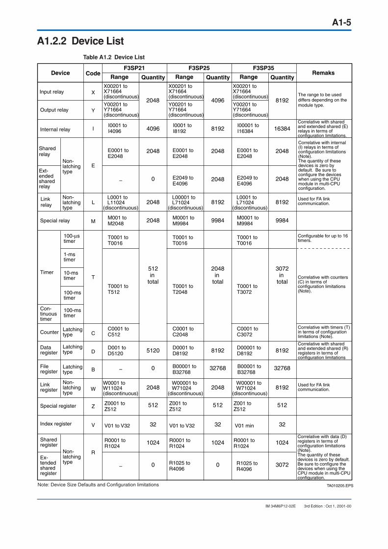
IM 34M6P12-02E 3rd Edition : Oct 1, 2001-00
A1.2.2 Device ListTable A1.2 Device List
Input relayX00201 to X71664 (discontinuous)
Y00201 to Y71664 (discontinuous)
The range to be used differs depending on the module type.
Output relay
Internal relay
Sharedrelay
Ext-ended sharedrelay
Linkrelay
Special relay
Timer
Con-tinuous timer
Counter
Dataregister
Fileregister
Linkregister
Special register
Index register
Shared register
Ex-tended sharedregister
I0001 to I4096
E0001 to E2048
L0001 to L11024(discontinuous)
M001 to M2048
T0001 to T0016
T0001 to T512
C0001 to C512
–
–
–
D001 toD5120
W0001 to W11024(discontinuous)
Z0001 to Z512
V01 to V32
Correlative with shared and extended shared (E) relays in terms of configuration limitations.
Used for FA link communication.
Used for FA link communication.
Correlative with data (D) registers in terms of configuration limitations (Note).The quantity of these devices is zero by default. Be sure to configure the devices when using the CPU module in multi-CPU configuration.
Configurable for up to 16 timers.
Correlative with counters (C) in terms of configuration limitations (Note).
Correlative with timers (T) in terms of configuration limitations (Note).
Correlative with shared and extended shared (R) registers in terms of configuration limitations
Correlative with internal (I) relays in terms of configuration limitations (Note).The quantity of these devices is zero by default. Be sure to configure the devices when using the CPU module in multi-CPU configuration.
R0001 to R1024
Non-latching type
Non-latching type
100-µs timer
1-ms timer
10-ms timer
100-ms timer
100-ms timer
Latching type
Latching type
Latching type
Non-latching type
Non-latching type
Device CodeRange Quantity
F3SP21
Range Quantity
F3SP25
Range Quantity
F3SP35
X
Y
I
E
L
M
T
C
D
B
W
Z
V
R
2048
4096
2048
0
2048
2048
512in
total
5120
0
2048
512
32
1024
0
X00201 to X71664 (discontinuous)
Y00201 to Y71664 (discontinuous)
I0001 to I8192
E0001 to E2048
E2049 to E4096
L00001 to L71024 (discontinuous)
M0001 to M9984
T0001 to T0016
T0001 to T2048
C0001 to C2048
D0001 toD8192
B00001 toB32768
B00001 toB32768
W00001 to W71024 (discontinuous)
Z001 to Z512
V01 to V32
R0001 to R1024
4096
8192
2048
2048
8192
9984
2048in
total
8192
32768
2048
512
32
1024
0
X00201 to X71664 (discontinuous)
Y00201 to Y71664 (discontinuous)
I00001 to I16384
E0001 to E2048
E2049 to E4096
L0001 to L71024 (discontinuous)
M0001 to M9984
T0001 to T0016
T0001 to T3072
C0001 to C3072
D00001 toD8192
W00001 to W71024 (discontinuous)
Z001 to Z512
V01 min
R0001 to R1024
R1025 to R4096
8192
16384
2048
2048
8192
9984
3072in
total
8192
32768
8192
512
32
1024
3072
TA010205.EPS
Remaks
R1025 to R4096
Note: Device Size Defaults and Configuration limitations

A1-6
IM 34M6P12-02E 3rd Edition : Oct 1, 2000-00
Device Code DeviceSize
Default
Configurationlimitations
DeviceSize
Default
Configurationlimitations
DeviceSize
Default
Configurationlimitations
F3SP21 F3SP25 F3SP35
Shared register
Extendedshared register
R
D
C
T
I
R
Shared relay
Extendedshared relay
E
E
Internal relay
Timer
Counter
Data register
4096
0
0
–
–
–
–
5120
256
256
8192
0
0
0
0
8192
1024
1024
16384
0
0
0
0
8192
1024
2048
Sum of internal relays and shared/extended shared relays: 4096 points max.Maximum number of shared/extended shared relays: 2048 points
Sum of internal relays and shared/extended shared relays: 8192 points max.Maximum number of shared/extended shared relays: 2048 points
Sum of internal relays and shared/extended shared relays: 16834 points max.Maximum number of shared/extended shared relays: 2048 points
Sum of timers and counters: 512 points max.Initial quantity of 1-ms timers: 0
Sum of timers and counters: 3072 points max.Initial quantity of 1-ms timers: zero
Sum of timers and counters: 2048 points max.
3072 points max.
2048 points max.
3072 points max.
2048 points max.
Sum of data registers and shared/extended shared registers: 5120 points max.Maximum number of shared/extended shared registers: 1024 points
Sum of data registers and shared/extended shared registers: 8192 points max.Maximum number of shared/extended shared registers: 1024 points
Sum of data registers and shared/extended shared registers: 8192 points max.Maximum number of shared/extended shared registers: 1024 points
TA010206.EPS
A1-7
IM 34M6P12-02E 3rd Edition : Oct 1, 2001-00
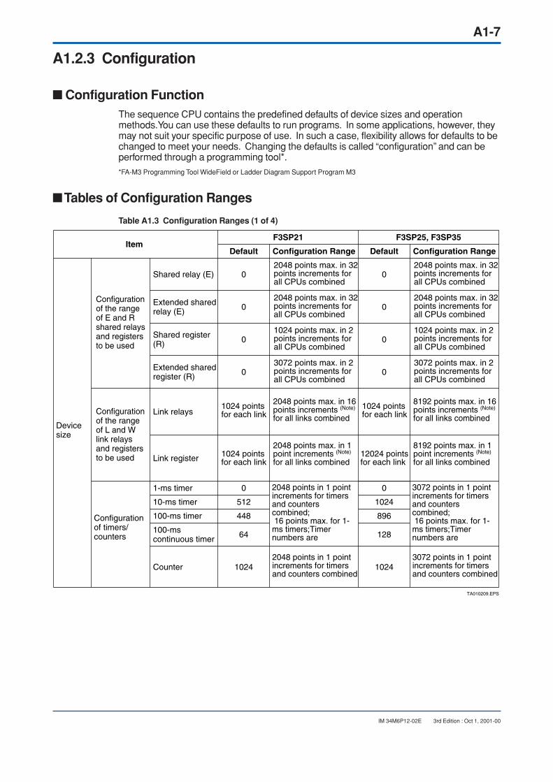
A1.2.3 Configuration
Configuration FunctionThe sequence CPU contains the predefined defaults of device sizes and operationmethods.You can use these defaults to run programs. In some applications, however, theymay not suit your specific purpose of use. In such a case, flexibility allows for defaults to bechanged to meet your needs. Changing the defaults is called “configuration” and can beperformed through a programming tool*.*FA-M3 Programming Tool WideField or Ladder Diagram Support Program M3
Tables of Configuration Ranges
Table A1.3 Configuration Ranges (1 of 4)
ItemF3SP25, F3SP35
Default
Device size
Link relays
Configuration of timers/counters
Link register
0
0
Shared relay (E)
Extended shared relay (E)
Shared register (R)
Extended shared register (R) 0
0
Configuration Range
TA010209.EPS
F3SP21
Default
02048 points max. in 32 points increments for all CPUs combined
Counter 10241024
02048 points max. in 32 points increments for all CPUs combined
03072 points max. in 2 points increments for all CPUs combined
01024 points max. in 2 points increments for all CPUs combined
Configuration Range
1024 points for each link
1024 points for each link
1024 points for each link
12024 points for each link
1-ms timer 00
10-ms timer 1024512
100-ms timer 896448
100-ms continuous timer 12864
Configuration of the range of E and R shared relays and registers to be used
2048 points max. in 16 points increments (Note) for all links combined
2048 points max. in 1 point increments (Note) for all links combined
2048 points in 1 point increments for timers and counters combined
2048 points in 1 point increments for timers and counters combined; 16 points max. for 1-ms timers;Timer numbers are
2048 points max. in 32 points increments for all CPUs combined
2048 points max. in 32 points increments for all CPUs combined
3072 points max. in 2 points increments for all CPUs combined
1024 points max. in 2 points increments for all CPUs combined
8192 points max. in 16 points increments (Note) for all links combined
8192 points max. in 1 point increments (Note) for all links combined
3072 points in 1 point increments for timers and counters combined
3072 points in 1 point increments for timers and counters combined; 16 points max. for 1-ms timers;Timer numbers are
Configuration of the range of L and W link relays and registers to be used

A1-8
IM 34M6P12-02E 3rd Edition : Oct 1, 2000-00
Table A1.3 Configuration Ranges (2 of 4)
ItemF3SP25, F3SP35
Default
Extended device configuration
Configuration Range
TA010210.EPS
F3SP21
Default
Internal relay (I) I0001 to I1024 Configurable in 32
points basis; continuous from the starting number
I0001 to I1024 Configurable in 32
points basis; continuous from the starting number
Configurable in 16 points basis (Note)
Configurable in 16points basis (Note)
Configurable in 1 point basis; continuous from the starting number
Configurable in 1 point basis; continuous from the starting number
Configurable in 2 points basis; continuous from the starting number (Note)
Configurable in 2 points basis; continuous from the starting number (Note)
Link register (W)
Non-latching type
Configurable in 16 points basis (Note)
Non-latching type
Configurable in 16 points basis (Note)
Configuration Range
Shared and extended shared relays (E)
Non-latching type
Non-latching type
Counter (C)All latched (C0001 to C1024)
All latched (C0001 to C1024)
Data register (D)
All latched (D00001 to D32768)
All latched (D00001 to D16384)
Shared and extended shared registers (R)
Non-latching type
Non-latching type
Link relay (L) Non-latching type
Non-latching type
Timer (T)
Non-latching type (except for continuous timers)
Non-latching type (except for continuous timers)
Range of devices to be latched in case of power failure
Note: The configuration range of each of the shared and extended shared relays and shared and extendedshared registers to be latched in case of power failure is assigned numbers continuous from the startingnumber. However, if the number of shared relays is smaller than 2048, the last of them is followed by thefirst extended shared relay numbered E2049. Likewise, if the number of shared registers is smaller than1024, the last of them is followed by the first extended shared register numbered R1025.
Example)In a case where there are 1024 shared relays and 2048 extended shared relays:f you define the starting number as 513 and the number of units as 1024 for the range of devices to belatched in case of power failure, then the devices included in the latching are:E513 to E1024 shared relays; andE2049 to E2560 extended shared relays.
Note: The configuration range of each link relay and register to be latched in case of power failure is assignednumbers continuous from the starting number.However, the following exceptions apply.
The number following L/W01024 is L/W10001.The number following L/W11024 is L/W20001.The number following L/W21024 is L/W30001.The number following L/W31024 is L/W40001.The number following L/W41024 is L/W50001.The number following L/W51024 is L/W60001.The number following L/W61024 is L/W70001.
(The rules noted above are true when the number of link relays or registers to be used is defined as 1024.If the number is 2048, the number following L/W02048 is L/W10001.)
Example)When there are 1024 link relays each for link 1, link 2 and link 3:If you define the starting number as 10513 and the number of units as 1024 for the range of devices to belatched in case of power failure, then the devices included in the latching are:L10513 to L11024 link relays for link 1; andL20001 to L20512 link relays for link 2.

A1-9
IM 34M6P12-02E 3rd Edition : Oct 1, 2001-00
Table A1.3 Configuration Ranges (3 of 4)
ItemDefault Configuration
RangeDefault Configuration
RangeDefault Configuration
Range
F3SP21 F3SP25 F3SP35
None
200ms
Unused
TA010211.EPS
Operation control
Initial data setting
Operation mode in case of failure
Data register (D)
Scan time monitoring time
Constant scan time
I/O module failure
Scan timeout
Subroutineerror
Interrupt error
Subunit transmissionline failure
I/O collation failure
Instruction processingfailure
Program execution mode
Momentarypower failuredetectionmode
I/O module
Effective only if F3PU10-0N, F3PU20-0N or F3PU26-0N power supply module is used.
Configurable for up to 1024 points continuously from the starting number; initial data configurable
Configurable from 10 to 200 ms in 10 ms increments
Configurable from 1.0 to 190.0 ms in 0.1 ms increments
Selectable from Stop and Continue options.
Selectable from Stop and Continue options.
Selectable from Stop and Continue options.
All or selected blocks are executed.
Standard or immediate detection mode
Reset/hold; configurable on amodule basis
DIOpoints
ROM
Output mode in caseof sequence stop
Data codetype
Input samplinginterval
BIN/BCD; configurable in 16 point increments
Data register (D) File register (B)
16 ms/1 ms; configurable on amodule basis
Devices' current values to be made resident in ROM
Configurable for up to 5120 points continuously from the starting number
Stop
Stop
Stop
Stop
Stop
Stop
Con-tinuation
Con-tinuation
Con-tinuation
All blocksareexecuted.
Reset
BIN
16ms
None
Standardmode
None None
200ms
Unused.
Configurable from 10 to 200 ms in 10 ms increments
200msConfigurable from 10 to 200 ms in 10 ms increments
Configurable from 1.0 to 190.0 ms in 0.1 ms increments
Unused.Configurable from 1.0 to 190.0 ms in 0.1 ms increments
All or selected blocks are executed.
Standard or immediate detection mode
Reset/hold; configurable on amodule basisBIN/BCD; configurable in 16 point increments16 ms/1 ms; configurable on amodule basis
Configurable for up to 5120 points continuously from the starting number
Stop
Stop
Stop
Stop
Stop
Stop
Stop
Stop
Stop
Stop
Stop
Stop
All blocksareexecuted.
All or selected blocks are executed.
All blocksareexecuted.
ResetReset/hold; configurable on amodule basis
Reset
BINBIN/BCD; configurable in 16 point increments
BIN
16ms16 ms/1 ms; configurable on amodule basis
16ms
None
Configurable for up to 5120 points continuously from the starting number
None
Standardmode
Standard or immediate detection mode
Standardmode
Configurable for up to 1024 points continuously from the starting number; initial data configurable
Configurable for up to 1024 points continuously from the starting number; initial data configurable
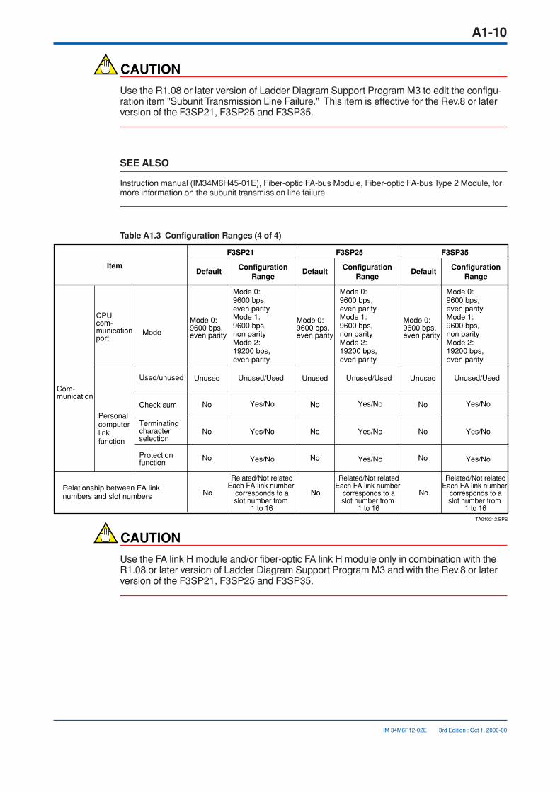
A1-10
IM 34M6P12-02E 3rd Edition : Oct 1, 2000-00
CAUTION
Use the R1.08 or later version of Ladder Diagram Support Program M3 to edit the configu-ration item "Subunit Transmission Line Failure." This item is effective for the Rev.8 or laterversion of the F3SP21, F3SP25 and F3SP35.
SEE ALSO
Instruction manual (IM34M6H45-01E), Fiber-optic FA-bus Module, Fiber-optic FA-bus Type 2 Module, formore information on the subunit transmission line failure.
Table A1.3 Configuration Ranges (4 of 4)
ItemDefault Configuration
RangeDefault Configuration
RangeDefault Configuration
Range
F3SP21 F3SP25 F3SP35
TA010212.EPS
Com-munication
CPU com-municationport
Mode 0:9600 bps,even parityMode 1:9600 bps,non parityMode 2:19200 bps,even parity
Mode 0:9600 bps,even parity
Mode 0:9600 bps,even parityMode 1:9600 bps,non parityMode 2:19200 bps,even parity
Mode 0:9600 bps,even parity
Mode 0:9600 bps,even parityMode 1:9600 bps,non parityMode 2:19200 bps,even parity
Mode 0:9600 bps,even parity Mode
Personalcomputerlinkfunction
Used/unused
Protection function
Check sum
Terminating character selection
Unused
No
No
No
No
Relationship between FA linknumbers and slot numbers
Unused/Used
Yes/No
Yes/No
Yes/No
Related/Not relatedEach FA link number
corresponds to aslot number from
1 to 16
Unused
No
No
No
No
Unused/Used
Yes/No
Yes/No
Yes/No
Unused
No
No
No
No
Unused/Used
Yes/No
Yes/No
Yes/No
Related/Not relatedEach FA link number
corresponds to aslot number from
1 to 16
Related/Not relatedEach FA link number
corresponds to aslot number from
1 to 16
CAUTION
Use the FA link H module and/or fiber-optic FA link H module only in combination with theR1.08 or later version of Ladder Diagram Support Program M3 and with the Rev.8 or laterversion of the F3SP21, F3SP25 and F3SP35.
A1-11
IM 34M6P12-02E 3rd Edition : Oct 1, 2001-00
CAUTION
For each of the F3LP02 FA link H modules and F3LP12 fiber-optic FA link H modules, youcan use a maximum of 2048 points of link relays and link registers. The configurationlimitations described below apply, however, if either of the following cases is true.
1. A case where a single CPU uses a combination of FA link H module and fiber-optic FAlink H modules, each configured with 2048 points of link relays/registers.
2. A case where a single CPU uses a combination of FA link H or fiber-optic FA link Hmodules configured with 1024 points of link relays/registers set for high-speedprocessing and FA link H or fiber-optic FA link H modules configured with 2048 pointsof link relays/registers set for normal-speed processing.
Configuration limitations:
For FA link 1, be sure to set the number of both link relays and link registers to 2048. If youset the number to 1024, the CPU does not operate correctly. If the number of both linkrelays and link registers is set to 0 for FA link 1, be sure to set the number to 2048 for FAlink 2.
Examples of Unallowable Configuration:
Link 1: [1024]; Link 2: [2048]; Link 3: . . .
Link 1: [ 0]; Link 2: [1024]; Link 3: [2048]; . . .
Link 1: [1024]; Link 2: [ 0]; Link 3: [2048]; . . .
Examples of Allowable Configuration:
Link 1: [2048]; Link 2: . . .
Link 1: [1024]; Link 2: [1024]; Link 3: . . .
Link 1: [ 0]; Link 2: [1024]; Link 3: [1024]; . . .
Link 1: [1024]; Link 2: [ 0]; Link 3: [1024]; . . .
Link 1: [ 0]; Link 2: [2048]; Link 3: . . .
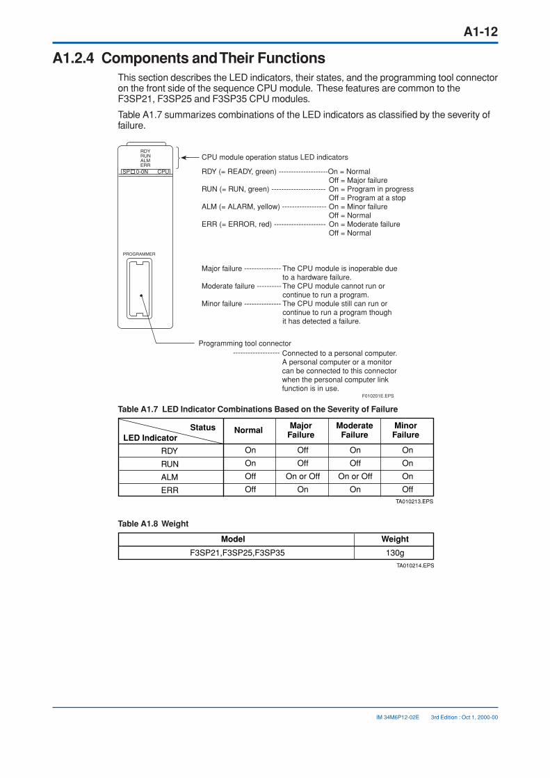
A1-12
IM 34M6P12-02E 3rd Edition : Oct 1, 2000-00
A1.2.4 Components and Their FunctionsThis section describes the LED indicators, their states, and the programming tool connectoron the front side of the sequence CPU module. These features are common to theF3SP21, F3SP25 and F3SP35 CPU modules.
Table A1.7 summarizes combinations of the LED indicators as classified by the severity offailure.
F010201E.EPS
SP 0-0N CPU
CPU module operation status LED indicators
RDY (= READY, green) --------------------On = Normal Off = Major failureRUN (= RUN, green) ---------------------- On = Program in progress Off = Program at a stopALM (= ALARM, yellow) ------------------ On = Minor failure Off = NormalERR (= ERROR, red) --------------------- On = Moderate failure Off = Normal
Major failure --------------- The CPU module is inoperable due to a hardware failure.
Moderate failure ---------- The CPU module cannot run or continue to run a program.
Minor failure --------------- The CPU module still can run or continue to run a program though it has detected a failure.
Programming tool connector ------------------- Connected to a personal computer.
A personal computer or a monitor can be connected to this connector when the personal computer link function is in use.
Table A1.7 LED Indicator Combinations Based on the Severity of Failure
Status Normal
On Off On On
On Off Off On
Off On or Off On or Off On
Off On On Off
MajorFailure
ModerateFailure
MinorFailureLED Indicator
RDY
RUN
ALM
ERRTA010213.EPS
Table A1.8 Weight
TA010214.EPS
Model Weight
F3SP21,F3SP25,F3SP35 130g
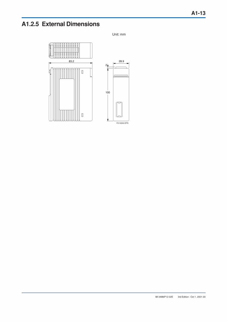
A1-13
IM 34M6P12-02E 3rd Edition : Oct 1, 2001-00
A1.2.5 External Dimensions
83.2 28.92
100
Unit: mm
F010202.EPS

A1-14
IM 34M6P12-02E 3rd Edition : Oct 1, 2000-00
A1.3 Basic Configuration
A1.3.1 UnitA unit is a system with its minimum configuration consisting of the following modules.Install these modules on the base module to compose the unit.
Table A1.9 Unit Components (Modules)
Name Description
Base module Five types are available depending on the number of modules to be mounted.
One power supply module must always be mounted on the base module.
Various types are available, including analog I/O and communication modules.
Power supply module
CPU module
I/O module
Special moduleTA010301.EPS
At least one CPU module is required. Several types are available depending on the functionality.
Various types are available depending on the type of I/O and the number of I/O points.
The location where you install a module is called a slot.
Main UnitInstall the power supply module in the leftmost slot of the base module and the CPU mod-ule in the slot on the immediate right of the power supply module. Then, install required I/Oand special modules in the remaining slots. A system with this configuration is called amain unit.
F010301.EPS
CPU module
Power supply module
I/O and special modules
Figure A1.1 Main Unit
SubunitA subunit is an I/O expansion unit. It is connected to the main unit through a fiber-optic FA-bus or fiber-optic FA-bus type 2. A maximum of seven subunits can be connected to themain unit and are identified by their unit numbers. With fiber-optic FA-bus type 2, you canseparate any single subunit into a maximum of eight stations. For more information on themethod of separation, see the instruction manual (IM34M6H45-01E), Fiber-optic FA-busModule, Fiber-optic FA-bus Type 2 Module.

A1-15
IM 34M6P12-02E 3rd Edition : Oct 1, 2001-00
A1.3.2 Slot NumberA slot number indicates the position of a slot where a module is installed. The slot numberis defined as a three-digit integer, as shown below.
F010302.EPS
Slot number
Slot positions 01 to 16 are assigned to the slot on the immediate right of the power supply module through to the rightmost slot of a base module.
Unit numberMain unit = 0Subunit = 1 to 7
Figure A1.2 Slot Numbers (1 of 2)

A1-16
IM 34M6P12-02E 3rd Edition : Oct 1, 2000-00
F010303.EPS
001 002 003 004 005 006 007 008 009 010 011 012 013 014 015 016
101 102 103 104 105 106 107 108 109 110 111 112 113 114 115 116
601 602 603 604 605 606 607 608 609 610 611 612 613 614 615 616
501 502 503 504 505 506 507 508 509 510 511 512 513 514 515 516
401 402 403 404 405 406 407 408 409 410 411 412 413 414 415 416
301 302 303 304 305 306 307 308 309 310 311 312 313 314 315 316
201 202 203 204 205 206 207 208 209 210 211 212 213 214 215 216
701 702 703 704 705 706 707 708 709 710 711 712 713 714 715 716
FA-M3 main unitSlot numbers 001 to 016
Subunit 1
Subunit 2
Subunit 3
Subunit 4
Subunit 5
Subunit 6
Subunit 7
Slot numbers 101 to 116
Slot numbers 201 to 216
Slot numbers 301 to 316
Slot numbers 401 to 416
Slot numbers 501 to 516
Slot numbers 601 to 616
Slot numbers 701 to 716
Power supply module
Power supply module
Power supply module
Power supply module
Power supply module
Power supply module
Power supply module
Power supply module
Add-on CPUs (three CPUs max.)
CPU module
Fiber-optic FA-bus type 2 module (can be installed in any position)
Figure A1.3 Slot Numbers (2 of 2)
Install fiber-optic FA-bus type 2 modules in both the main unit and a subunit and connectthese modules with a fiber-optic cable. You can attach a maximum of seven subunits to themain unit. Subunit numbers are determined by setting the rotary switch on the front panelof each fiber-optic FA-bus type 2 module.
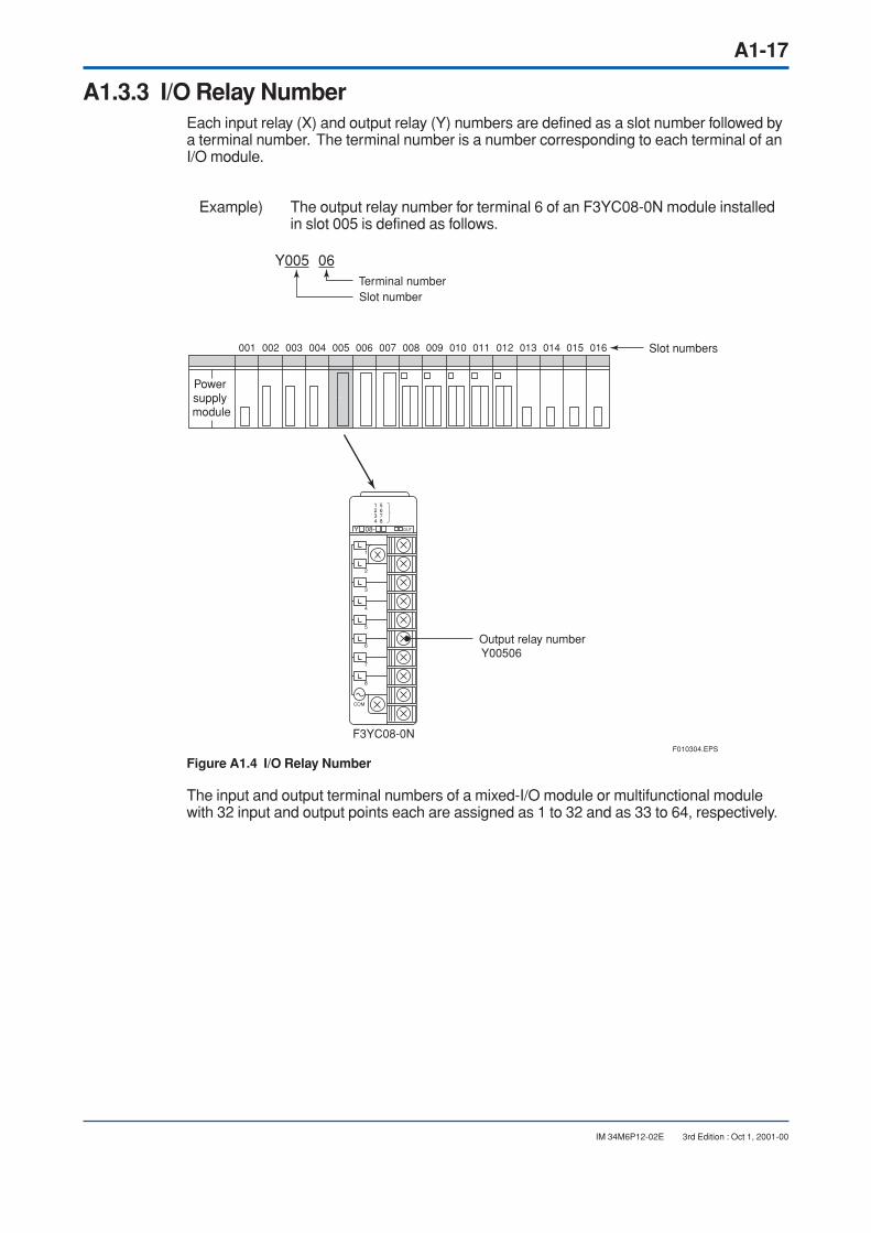
A1-17
IM 34M6P12-02E 3rd Edition : Oct 1, 2001-00
A1.3.3 I/O Relay NumberEach input relay (X) and output relay (Y) numbers are defined as a slot number followed bya terminal number. The terminal number is a number corresponding to each terminal of anI/O module.
Example) The output relay number for terminal 6 of an F3YC08-0N module installedin slot 005 is defined as follows.
F010304.EPS
Y
001 002 003 004 005
Y005 06
006 007 008 009 010 011 012 013 014 015 016
Terminal numberSlot number
Slot numbers
Power supply module
Output relay number Y00506
OUT08-
F3YC08-0N
Figure A1.4 I/O Relay Number
The input and output terminal numbers of a mixed-I/O module or multifunctional modulewith 32 input and output points each are assigned as 1 to 32 and as 33 to 64, respectively.

Blank Page
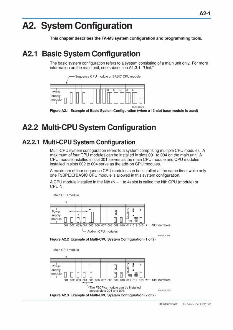
A2-1
IM 34M6P12-02E 3rd Edition : Oct 1, 2001-00
A2. System ConfigurationThis chapter describes the FA-M3 system configuration and programming tools.
A2.1 Basic System ConfigurationThe basic system configuration refers to a system consisting of a main unit only. For moreinformation on the main unit, see subsection A1.3.1, "Unit."
F020101.EPS
Sequence CPU module or BASIC CPU module
Power supply module
Figure A2.1 Example of Basic System Configuration (when a 13-slot base module is used)
A2.2 Multi-CPU System Configuration
A2.2.1 Multi-CPU System ConfigurationMulti-CPU system configuration refers to a system comprising multiple CPU modules. Amaximum of four CPU modules can be installed in slots 001 to 004 on the main unit. ACPU module installed in slot 001 serves as the main CPU module and CPU modulesinstalled in slots 002 to 004 serve as the add-on CPU modules.
A maximum of four sequence CPU modules can be installed at the same time, while onlyone F3BP BASIC CPU module is allowed in this system configuration.
A CPU module installed in the Nth (N = 1 to 4) slot is called the Nth CPU (module) orCPU N.
F020201.EPS
Main CPU module
Slot numbers
Add-on CPU modules
001 002 003 004 005 006 007 008 009 010 011 012 013
Power supply module
Figure A2.2 Example of Multi-CPU System Configuration (1 of 2)
F020201.EPS
Main CPU module
Slot numbers
The F3CPxx module can be installed across slots 004 and 005.
001 002 003 004 005 006 007 008 009 010 011 012 013
Power supply module
Figure A2.3 Example of Multi-CPU System Configuration (2 of 2)

A2-2
IM 34M6P12-02 3rd Edition : Oct 1, 2001-00
CAUTION
Be careful not to install any CPU module in the 5th or later slot and turn on the power.Otherwise, the memory is cleared and reverts to the factory settings.
See Also
Subsection 1.1.2, “Limitation on Module Installation,” of Hardware Manual (IM34M6C11-01E) , forinformation about limitations on the combination of a main CPU module and add-on CPU modules.
A2.2.2 Handling I/O Modules in Multi-CPU System
Input ModulesWith input modules, you can read input data through multiple sequence CPUs. To do this,configure the sequence CPUs so that they share the same input sampling interval for theinput module in question. Be careful, as the sampling interval that you can set variesdepending on the type of sequence CPU.
Output Modules and Multifunctional Modules Containing YOutput Relays
It is not possible to share the same output module among multiple sequence CPUs. Con-figure the sequence CPU that does not use the output module so that the output module isset to “unused”.
CAUTION
In multi-CPU system configuration, it is not possible for two or more sequence CPUs toshare the same output relay of any single output module or multifunctional module withoutput relays Y. Configure the sequence CPU that does not use the outputmodule so that the output relays of the output module is set to “Unused” on 16 points basis.
Note again that a CPU module installed in the Nth (N = 1 to 4) slot is called the Nth CPU(module) or CPU N.
CAUTION
Be careful not to install any sequence CPU module in the 5th or later slot and turn on thepower. Otherwise, the memory is cleared and reverts to the factory settings.
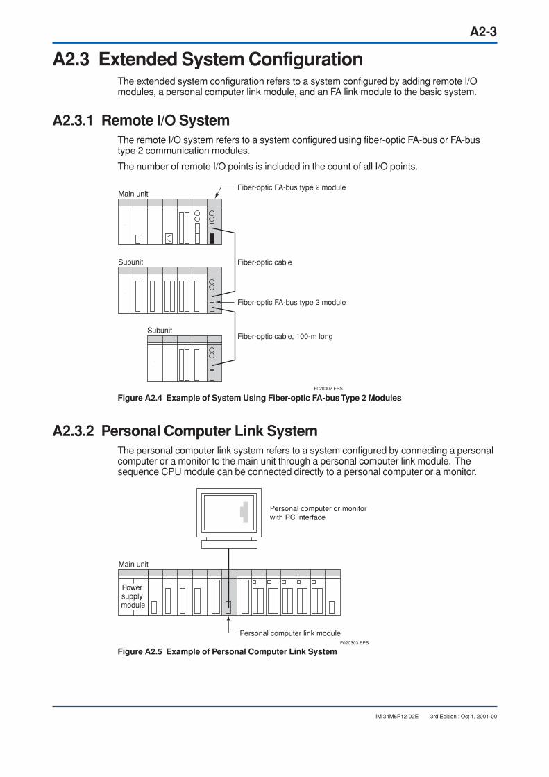
A2-3
IM 34M6P12-02E 3rd Edition : Oct 1, 2001-00
A2.3 Extended System ConfigurationThe extended system configuration refers to a system configured by adding remote I/Omodules, a personal computer link module, and an FA link module to the basic system.
A2.3.1 Remote I/O SystemThe remote I/O system refers to a system configured using fiber-optic FA-bus or FA-bustype 2 communication modules.
The number of remote I/O points is included in the count of all I/O points.
F020302.EPS
Main unit
Subunit
Subunit
Fiber-optic FA-bus type 2 module
Fiber-optic cable
Fiber-optic FA-bus type 2 module
Fiber-optic cable, 100-m long
Figure A2.4 Example of System Using Fiber-optic FA-bus Type 2 Modules
A2.3.2 Personal Computer Link SystemThe personal computer link system refers to a system configured by connecting a personalcomputer or a monitor to the main unit through a personal computer link module. Thesequence CPU module can be connected directly to a personal computer or a monitor.
F020303.EPS
Personal computer or monitor with PC interface
Main unit
Personal computer link module
Power supply module
Figure A2.5 Example of Personal Computer Link System
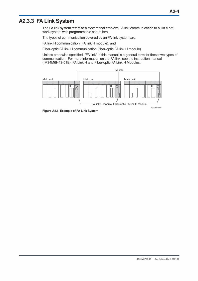
A2-4
IM 34M6P12-02 3rd Edition : Oct 1, 2001-00
A2.3.3 FA Link SystemThe FA link system refers to a system that employs FA link communication to build a net-work system with programmable controllers.
The types of communication covered by an FA link system are:
FA link H communication (FA link H module), and
Fiber-optic FA link H communication (fiber-optic FA link H module).
Unless otherwise specified, "FA link" in this manual is a general term for these two types ofcommunication. For more information on the FA link, see the instruction manual(IM34M6H43-01E), FA Link H and Fiber-optic FA Link H Modules.
F020304.EPS
Main unit Main unit
FA link
Main unit
FA link H module, Fiber-optic FA link H module
Figure A2.6 Example of FA Link System

A2-5
IM 34M6P12-02E 3rd Edition : Oct 1, 2001-00
A2.4 Programming ToolsThe FA-M3 programming tool WideField , or simply WideField, and Ladder Diagram Sup-port Program M3 are available as programming tools for the FA-M3 system.
A2.4.1 WideFieldThe table below presents an overview of WideField.
Description Software Model Supported CPUs
FA-M3 Programming Tool WideField SF610-ECW
F3SP05 F3SP38F3SP21 F3SP53F3SP25 F3SP58F3SP28 F3FP36F3SP35
TA020401.EPS
FA020401.EPS
Personal computer
Power supply module
Sequence CPU module
Figure A2.7 Overview of WideField
Object LadderWideField defines "blocks" and "macros" that compose a ladder program as "objects," aterm commonly used in the computing world. The object-oriented ladder language as-sumes responsibility for a given function and features a high degree of independence.Consequently, the language offers higher productivity and better maintainability than astructured programming language. It is therefore effective for the reuse of ladder programs.
Features
Treatment as Components
Blocks can be reused as components. Separately define devices that are used within ablock only. WideField eliminates the chance of using the same device twice and makes iteasy to recombine blocks. You can also break down macro functions into components.
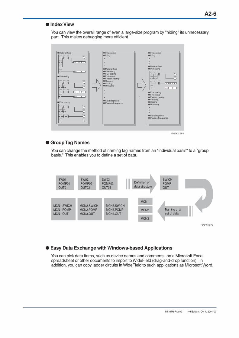
A2-6
IM 34M6P12-02 3rd Edition : Oct 1, 2001-00
Index View
You can view the overall range of even a large-size program by "hiding" its unnecessarypart. This makes debugging more efficient.
F020402.EPS
I*****
I*****
I*****
I*****
Y*****
Y*****
Y*****
Y*****
I*****
I*****
I*****
I*****
I*****
I*****
I*****
I*****
I*****
Y*****
Y*****
I*****
I*****
I*****
I*****
I*****
I*****
I*****
I*****
I***** Y*****I***** I*****
CAL =
MOVE
+
I*****
I*****
I*****
I*****
Y*****
Y*****
I*****
I*****
I*****
I*****
I*****
CAL =
MOVE
+
CAL =
MOVE
+
Material feed Initialization Idling
Fault-diagnosis Power-off sequence
Material feed Preheating Flux coating Finish coat Fixation heating Cleaning Cooling Unloading
Preheating
Flux coating
•
•
•
•
•
•
Initialization Idling
Fault-diagnosis Power-off sequence
Material feed Preheating
•••
•••
Flux coating Finish coat Fixation heating Cleaning Cooling Unloading
Group Tag Names
You can change the method of naming tag names from an "individual basis" to a "groupbasis." This enables you to define a set of data.
SW01POMP01OUT01
MCN1.SWICHMCN1.POMPMCN1.OUT
MCN2.SWICHMCN2.POMPMCN3.OUT
MCN3.SWICHMCN3.POMPMCN3.OUT
SW02POMP02OUT02
SW03POMP03OUT03
SWICHPOMPOUT
Definition of data structure
Naming of a set of data
MCN1
MCN2
MCN3
F040403.EPS
Easy Data Exchange with Windows-based Applications
You can pick data items, such as device names and comments, on a Microsoft Excelspreadsheet or other documents to import to WideField (drag-and-drop function). Inaddition, you can copy ladder circuits in WideField to such applications as Microsoft Word.
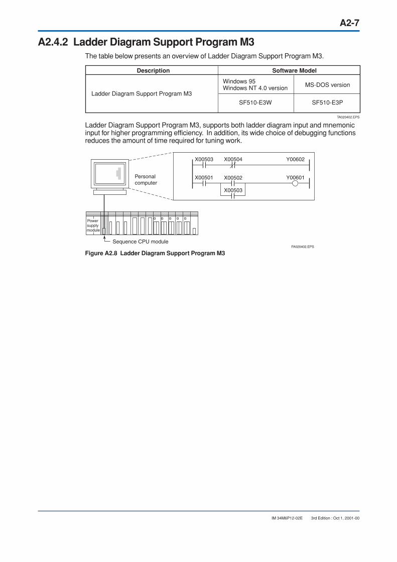
A2-7
IM 34M6P12-02E 3rd Edition : Oct 1, 2001-00
A2.4.2 Ladder Diagram Support Program M3The table below presents an overview of Ladder Diagram Support Program M3.
Description Software Model
Ladder Diagram Support Program M3
Windows 95Windows NT 4.0 version
TA020402.EPS
MS-DOS version
SF510-E3W SF510-E3P
Ladder Diagram Support Program M3, supports both ladder diagram input and mnemonicinput for higher programming efficiency. In addition, its wide choice of debugging functionsreduces the amount of time required for tuning work.
FA020402.EPS
Personalcomputer
X00503 X00504
X00501 X00502
X00503
Y00602
Y00601
Power supply module
Sequence CPU module
Figure A2.8 Ladder Diagram Support Program M3

Blank Page
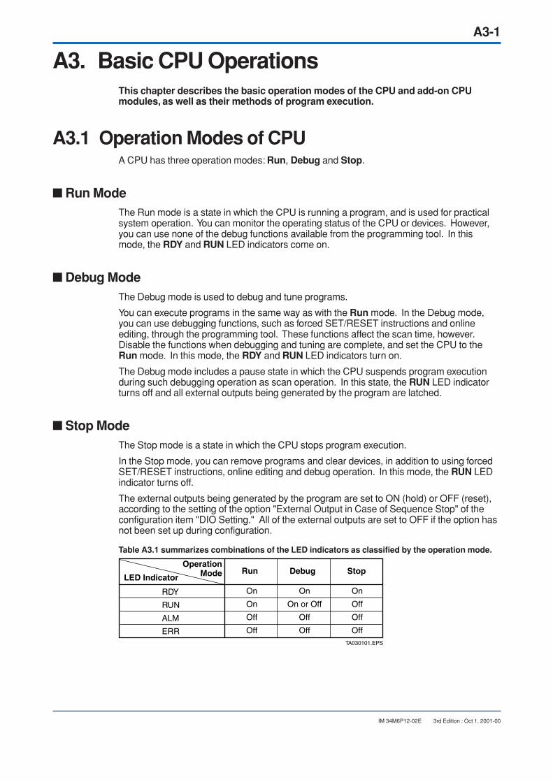
A3-1
IM 34M6P12-02E 3rd Edition : Oct 1, 2001-00
A3. Basic CPU OperationsThis chapter describes the basic operation modes of the CPU and add-on CPUmodules, as well as their methods of program execution.
A3.1 Operation Modes of CPUA CPU has three operation modes: Run, Debug and Stop.
Run ModeThe Run mode is a state in which the CPU is running a program, and is used for practicalsystem operation. You can monitor the operating status of the CPU or devices. However,you can use none of the debug functions available from the programming tool. In thismode, the RDY and RUN LED indicators come on.
Debug ModeThe Debug mode is used to debug and tune programs.
You can execute programs in the same way as with the Run mode. In the Debug mode,you can use debugging functions, such as forced SET/RESET instructions and onlineediting, through the programming tool. These functions affect the scan time, however.Disable the functions when debugging and tuning are complete, and set the CPU to theRun mode. In this mode, the RDY and RUN LED indicators turn on.
The Debug mode includes a pause state in which the CPU suspends program executionduring such debugging operation as scan operation. In this state, the RUN LED indicatorturns off and all external outputs being generated by the program are latched.
Stop ModeThe Stop mode is a state in which the CPU stops program execution.
In the Stop mode, you can remove programs and clear devices, in addition to using forcedSET/RESET instructions, online editing and debug operation. In this mode, the RUN LEDindicator turns off.
The external outputs being generated by the program are set to ON (hold) or OFF (reset),according to the setting of the option "External Output in Case of Sequence Stop" of theconfiguration item "DIO Setting." All of the external outputs are set to OFF if the option hasnot been set up during configuration.
Table A3.1 summarizes combinations of the LED indicators as classified by the operation mode.
OperationMode Run
On On On
On On or Off Off
Off Off Off
Off Off Off
Debug StopLED Indicator
RDY
RUN
ALM
ERRTA030101.EPS
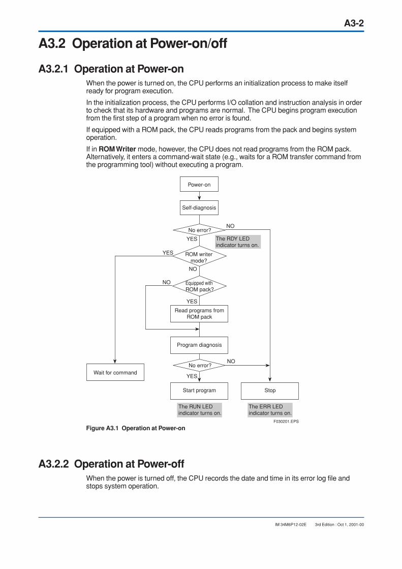
A3-2
IM 34M6P12-02E 3rd Edition : Oct 1, 2001-00
A3.2 Operation at Power-on/off
A3.2.1 Operation at Power-onWhen the power is turned on, the CPU performs an initialization process to make itselfready for program execution.
In the initialization process, the CPU performs I/O collation and instruction analysis in orderto check that its hardware and programs are normal. The CPU begins program executionfrom the first step of a program when no error is found.
If equipped with a ROM pack, the CPU reads programs from the pack and begins systemoperation.
If in ROM Writer mode, however, the CPU does not read programs from the ROM pack.Alternatively, it enters a command-wait state (e.g., waits for a ROM transfer command fromthe programming tool) without executing a program.
YES
YES
YES
NO
YES
NO
NO
NO
The RUN LED indicator turns on.
The ERR LED indicator turns on.
StopStart program
Program diagnosis
Read programs from ROM pack
Equipped with ROM pack?
ROM writer mode?
Wait for commandNo error?
No error?
Self-diagnosis
Power-on
F030201.EPS
The RDY LED indicator turns on.
Figure A3.1 Operation at Power-on
A3.2.2 Operation at Power-offWhen the power is turned off, the CPU records the date and time in its error log file andstops system operation.
A3-3
IM 34M6P12-02E 3rd Edition : Oct 1, 2001-00
A3.3 Operation in Case of Momentary or CompletePower Failure
A3.3.1 Operation in Case of Momentary Power FailureThere are two types of power failure detection mode for detecting a momentary powerfailure: the standard mode and the immediate detection mode.
The CPU operates differently in case of a momentary power failure, depending on the typeof power failure detection mode selected.
The immediate detection mode can be selected by configuration only when the F3PU10-0N, F3PU20-0N or F3PU26-0N power supply module is used.
Standard ModeIf a momentary power failure occurs, the CPU records the date and time in its error log file.The CPU suspends processing until it recovers from the power failure. This causes a delayin the scan time and timer update process.
When the power has recovered, the CPU restarts at the point where it suspendedprocessing.
A program can cope with a momentary power failure since its occurrence is reflected on aspecial relay (M195).
AC voltage
Program execution
InterruptionF030301.EPS
Power failure detection level
Figure A3.2 Operation in Case of Momentary Power Failure
Immediate Detection ModeIf a momentary power failure occurs, the CPU records the date and time in its error log file.The CPU suspends processing until it recovers from the power failure. At this point theCPU sets the external outputs being generated by a program to OFF, and actuates the FAILcontact.
When the power has recovered, the CPU undergoes a reset-and-start sequence andbegins executing the program from its start.
A3.3.2 Specifying the Momentary Power Failure Detection ModeThis configuration item defines the type of momentary power failure detection mode. Youcan select either the standard mode or the immediate detection mode. The default is thestandard mode. For more information on each of these modes, see Hardware Manual(IM34M6C11-01E).
CAUTION
If your system has multi-CPU configuration and you have selected the immediate detectionmode, set all of the CPU modules to this mode.
A3-4
IM 34M6P12-02E 3rd Edition : Oct 1, 2001-00
A3.3.3 Operation in Case of Complete Power FailureIf a complete power failure occurs, the CPU operates as it does at power-off.
You can configure the types and ranges of devices to be latched in case of this type ofpower failure. This strategy allows the CPU to restart, when it recovers from the powerfailure, at the point where it suspended processing.
When the power has recovered, the CPU executes the program from its start.
A3.3.4 Specifying the Range of Devices to Be Latched in Case ofComplete Power Failure
This configuration item sets the range of devices to be latched in case of a complete powerfailure. Specify the starting number and the number of units for each device type.
Table A3.2 shows the default setting and the configurable range of each device type.
Table A3.2 Configuration of Devices to Be Latched in Case of Complete Power Failure (for F3SP21 and F3SP25)
ItemF3SP25
Default Configuration Range
TA030301.EPS
F3SP21Default
Internal relay (I) I0001 to I1024
Configurable on 32 points basis; continuous from the starting number (*1)
I0001 to I1024
Configurable on 32 points basis; continuous from the starting number
Configurable on 16 points basis (*2)
(Discontinuous)
Configurable on 16 points basis(Discontinuous)
Configurable on 1 pointbasis; continuous from the starting number
Configurable on 1 point basis; continuous from the starting number
Configurable on 2 points basis; continuous from the starting number
Configurable on 2 points basis; continuous from the starting number
Link register (W) Non-latching type
Configurable on 16 points basis (*2)
(Discontinuous)Non-latching type
Configurable on 16 points basis
Configuration Range
Shared and extendedshared relays (E)
Non-latching type
Non-latching type
Counter (C)All latched (C0001 to C1024)
All latched (C0001 to C256)
Data register (D)All latched (D0001 to D8192)
All latched (D0001 to D5120)
Shared registers (R)Non-latching type
Non-latching type
Link relay (L) Non-latching type
Non-latching type
Timer (T)
Non-latching type (except for continuous timers)
Non-latching type (except for continuous timers)
For notes *1 and *2, see those shown below Table A3.3.

A3-5
IM 34M6P12-02E 3rd Edition : Oct 1, 2001-00
Table A3.3 Configuration of Devices to Be Latched in Case of Complete Power Failure (for F3SP35)
ItemF3SP35
Default Configuration Range
TA030302.EPS
Internal relay (I) I0001 to I1024
Configurable on 32 points basis; continuous from the starting number (*1)
Configurable on 16 points basis (*2)
(Discontinuous)
Configurable on 1 pointbasis; continuous from the starting number
Configurable on 2 points basis; continuous from the starting number
Link register (W) Non-latching type
Configurable on 16 points basis (*2)
(Discontinuous)
Shared relays (E) Non-latching type
Counter (C)All latched (C0001 to C1024)
Data register (D)All latched (D0001 to D8192)
Shared registers (R) Non-latching type
Link relay (L) Non-latching type
Timer (T)
Non-latching type (except for continuous timers)
*1: If the upper limit of the range of shared relays to be used is smaller than E2049, the last of their numbers is followed bythe first of the extended shared relay numbers. Likewise, if the upper limit of shared registers to be used is smaller thanR1025, the last of their numbers is followed by the first of the extended shared register numbers.
*2: The configuration ranges of link relays and registers to be latched in case of power failure are assigned numberscontinuous from their starting numbers. However, the following exceptions apply.
The number following L/W01024 is L/W10001The number following L/W11024 is L/W20001The number following L/W21024 is L/W30001The number following L/W31024 is L/W40001The number following L/W41024 is L/W50001The number following L/W51024 is L/W60001The number following L/W61024 is L/W70001
These rules are true when the number of link relays or registers to be used is defined as 1024 (default). If the number is 2048, the number following n2048 is n0001.
A3-6
IM 34M6P12-02E 3rd Edition : Oct 1, 2001-00
A3.4 Computation MethodThe CPU employs a stored-program iterative computation method.
In this method, a created program is stored beforehand in the memory of the sequenceCPU module. The CPU executes instructions, one at a time, from the first step of theprogram. After executing the END instruction, the CPU performs required processes, suchas self-diagnosis. It then repeats the instructions from the first step.
Each of these iterative cycles is called “one scan” and the time required for one scan iscalled a “scan time.”
In the case of the F3SP21, F3SP25 and F3SP35 modules, the CPU executes instructionsand peripheral processes concurrently to perform each scan in a shorter time.
Common processing, instruction execution, input refreshing, output refreshing, andsynchronization processing are classified as a system of control-related processes, whiletool service, link service, CPU service, link refreshing, and shared refreshing are classifiedas a system of peripheral processes. The CPU performs these two kinds of processesconcurrently and separately to speed up the control-related processes.
Common processing
Instruction execution
Synchronization processing
One scanCommand processing• Tool service• Link service• CPU service
Shared refreshing
F030401.EPS
If synchronization processing begins, any peripheral process is interrupted temporarily and resumes at the next scan.
Control-related process
Peripheral process
Peripheral processes
Link refreshingPeripheral processes
are performed within this time range.
Input refreshing
Output refreshing
Figure A3.3 Computation Method

A3-7
IM 34M6P12-02E 3rd Edition : Oct 1, 2001-00
System of Control-related Processes
This system performs basic operations of the sequence CPU, such as instruction executionand I/O refreshing. In the case of the F3SP21, F3SP25 and F3SP35 sequence CPUs,execution of the system of control-related processes is called one scan, and the executiontime required by the system is usually called a scan time.
System of Peripheral Processes
This system supports programming tools and performs communication between the CPUand a personal computer or an FA link module.
The system of peripheral processes is concurrent with and independent of the system ofcontrol-related processes. Therefore, neither the number of modules connected nor thecontent of each peripheral process affects the way the system of control-related processesworks.
Synchronization between Systems of Control-related Processes andPeripheral Processes
The system of peripheral processes is concurrent with and independent of the system ofcontrol-related processes. For processes related to operation control (e.g., run or stop) orprocesses requiring the simultaneity of data, however, the CPU synchronizes these twosystems using a synchronization process included in the system of control-relatedprocesses.
The time required for the synchronization process varies depending on its content. Itaffects the scan time when you use a debugging function, such as online editing.
CAUTION
If the ratio of the instruction execution time to the scan time is too small, you may fail tosecure a time long enough to execute the system of peripheral processes. Consequently,the responses of link refreshing, shared refreshing, tool service, link service and CPUservice will become extremely slow. If this happens, 1) use a constant scan with an intervalsomewhat longer than the normal scan time, or 2) define the peripheral processing time tosecure a time long enough to execute the system of peripheral processes.
A3-8
IM 34M6P12-02E 3rd Edition : Oct 1, 2001-00
A3.5 Method of I/O Processing
A3.5.1 Method of I/O ProcessingAs the method of I/O processing, the CPU uses batch refreshing.
In this method, the CPU acquires all data changes in the input module into the input-relay(X) area of the CPU's data memory before executing each scan.
Thus, the CPU uses data contained in this area when performing computations.
Computation results are output to the output-relay (Y) area of the CPU's data memory eachtime a computation is performed. The results are sent to the output module, collectivelyand concurrently with the execution of instructions in the next scan.
X00502
X00501
X00503
I0002 L0001
I0001
X00502
I0100
Y00602
Y00601
Y00603
Y00604
External input instrument
External output instrument
CPU's data memory
Input refreshing
Output-relay (Y) area
Computation results
Output refreshing
Execution of computations
F030601.EPS
Input-relay (X) area
CPU's data memory
Figure A3.4 Method of I/O Processing
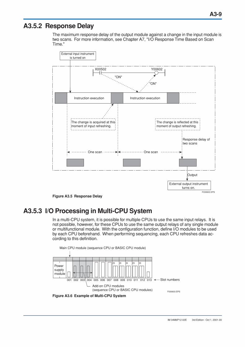
A3-9
IM 34M6P12-02E 3rd Edition : Oct 1, 2001-00
A3.5.2 Response DelayThe maximum response delay of the output module against a change in the input module istwo scans. For more information, see Chapter A7, "I/O Response Time Based on ScanTime."
X00502 Y00602
External input instrument is turned on
External output instrument turns on.
Response delay of two scans
The change is acquired at this moment of input refreshing.
The change is reflected at this moment of output refreshing.
Output
"ON"
"ON"
Instruction execution Instruction execution
F030602.EPS
One scan One scan
Figure A3.5 Response Delay
A3.5.3 I/O Processing in Multi-CPU SystemIn a multi-CPU system, it is possible for multiple CPUs to use the same input relays. It isnot possible, however, for these CPUs to use the same output relays of any single moduleor multifunctional module. With the configuration function, define I/O modules to be usedby each CPU beforehand. When performing sequencing, each CPU refreshes data ac-cording to this definition.
F030603.EPS
Main CPU module (sequence CPU or BASIC CPU module)
Power supply module
Slot numbers
Add-on CPU modules (sequence CPU or BASIC CPU modules)
Figure A3.6 Example of Multi-CPU System
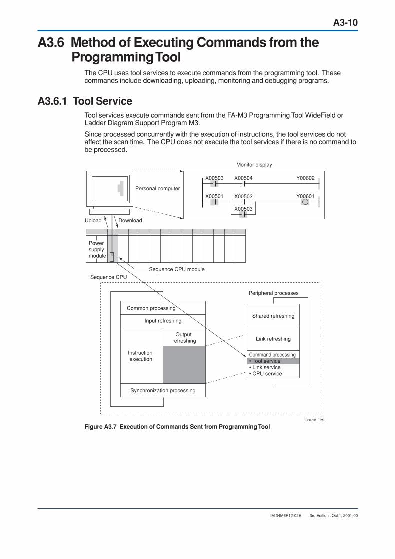
A3-10
IM 34M6P12-02E 3rd Edition : Oct 1, 2001-00
A3.6 Method of Executing Commands from theProgramming Tool
The CPU uses tool services to execute commands from the programming tool. Thesecommands include downloading, uploading, monitoring and debugging programs.
A3.6.1 Tool ServiceTool services execute commands sent from the FA-M3 Programming Tool WideField orLadder Diagram Support Program M3.
Since processed concurrently with the execution of instructions, the tool services do notaffect the scan time. The CPU does not execute the tool services if there is no command tobe processed.
X00503 X00504
X00501 X00502
X00503
Y00602
Y00601
F030701.EPS
Monitor display
Personal computer
DownloadUpload
Power supply module
Sequence CPU module
Sequence CPU
Common processing
Peripheral processes
Input refreshing
Output refreshing
Instruction execution
Synchronization processing
Shared refreshing
Link refreshing
Command processing• Tool service• Link service• CPU service
Figure A3.7 Execution of Commands Sent from Programming Tool
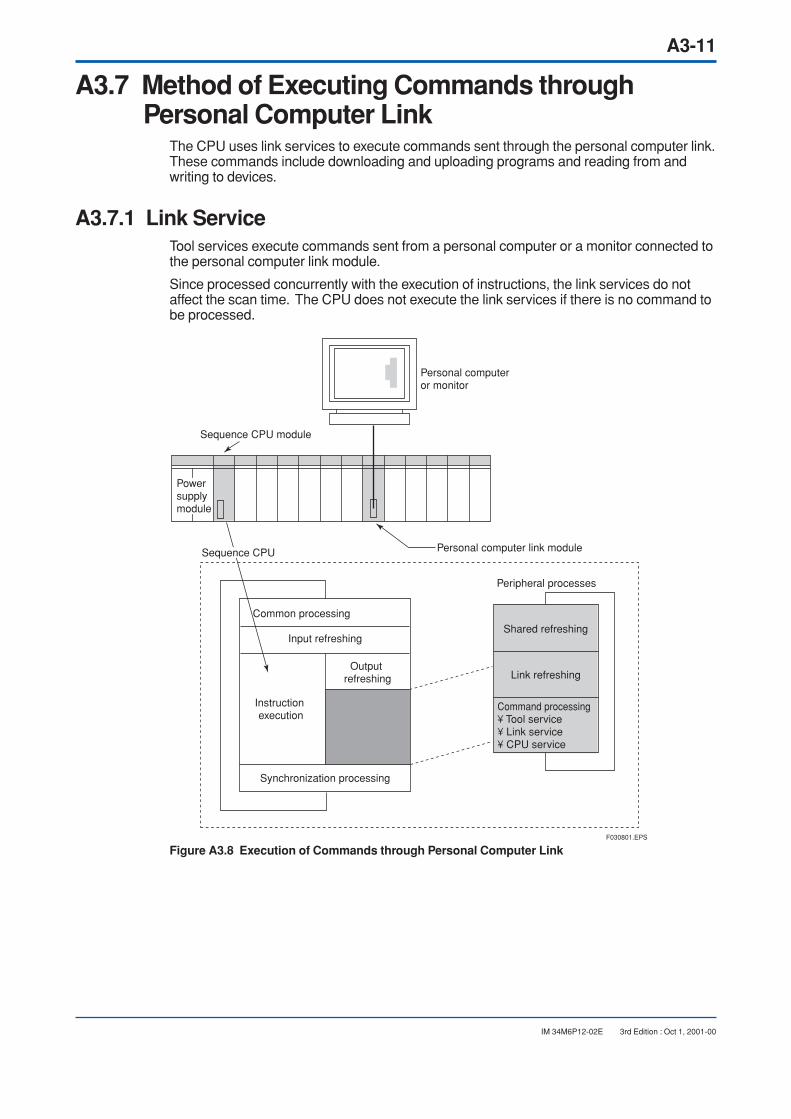
A3-11
IM 34M6P12-02E 3rd Edition : Oct 1, 2001-00
A3.7 Method of Executing Commands throughPersonal Computer Link
The CPU uses link services to execute commands sent through the personal computer link.These commands include downloading and uploading programs and reading from andwriting to devices.
A3.7.1 Link ServiceTool services execute commands sent from a personal computer or a monitor connected tothe personal computer link module.
Since processed concurrently with the execution of instructions, the link services do notaffect the scan time. The CPU does not execute the link services if there is no command tobe processed.
F030801.EPS
Personal computeror monitor
Power supply module
Personal computer link module
Common processing
Peripheral processes
Input refreshing
Output refreshing
Instruction execution
Synchronization processing
Shared refreshing
Link refreshing
Command processing¥ Tool service¥ Link service¥ CPU service
Sequence CPU
Sequence CPU module
Figure A3.8 Execution of Commands through Personal Computer Link
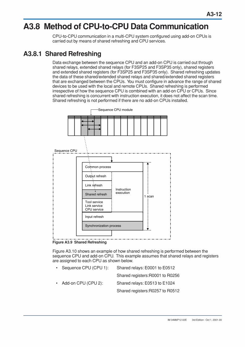
A3-12
IM 34M6P12-02E 3rd Edition : Oct 1, 2001-00
A3.8 Method of CPU-to-CPU Data CommunicationCPU-to-CPU communication in a multi-CPU system configured using add-on CPUs iscarried out by means of shared refreshing and CPU services.
A3.8.1 Shared RefreshingData exchange between the sequence CPU and an add-on CPU is carried out throughshared relays, extended shared relays (for F3SP25 and F3SP35 only), shared registersand extended shared registers (for F3SP25 and F3SP35 only). Shared refreshing updatesthe data of these shared/extended shared relays and shared/extended shared registersthat are exchanged between the CPUs. You must configure in advance the range of shareddevices to be used with the local and remote CPUs. Shared refreshing is performedirrespective of how the sequence CPU is combined with an add-on CPU or CPUs. Sinceshared refreshing is concurrent with instruction execution, it does not affect the scan time.Shared refreshing is not performed if there are no add-on CPUs installed.
Common process
Output refresh
Input refresh
Synchronization process
Instructionexecution
Link refresh
Shared refresh
Tool serviceLink serviceCPU service
1 scan
Sequence CPU
Sequence CPU module
Figure A3.9 Shared Refreshing
Figure A3.10 shows an example of how shared refreshing is performed between thesequence CPU and add-on CPU. This example assumes that shared relays and registersare assigned to each CPU as shown below.
• Sequence CPU (CPU 1): Shared relays: E0001 to E0512
Shared registers:R0001 to R0256
• Add-on CPU (CPU 2): Shared relays: E0513 to E1024
Shared registers:R0257 to R0512

A3-13
IM 34M6P12-02E 3rd Edition : Oct 1, 2001-00
E0001 X00504
X00501 T001
X00503
E0513
X00502
X00501 E0513 E0001
MOV $100 R0001
MOV R0001 D0001
CPU 1Shared - relay area
CPU 1Shared - register area
CPU 2Shared - relay area
CPU 2Shared - register area
CPU 1Shared - relay area
CPU 1Shared - register area
CPU 2Shared - relay area
CPU 2Shared - register area
CPU 1Shared refreshCPU 2
CPU 1
CPU 2Shared refresh
Figure A3.10 Shared Refreshing
CAUTION
Shared relays/registers and extended shared relays/registers are refreshed asynchro-nously with scans performed by each CPU. The simultaneity of data is therefore not guar-anteed.

A3-14
IM 34M6P12-02E 3rd Edition : Oct 1, 2001-00
A3.8.2 CPU ServiceCPU services exchange data and process commands, such as starting the program,between the sequence CPU and a BASIC CPU.
CPU services are provided irrespective of how the sequence CPU is combined with anadd-on CPU or CPUs. Since processed concurrently with the execution of instructions, theCPU services do not affect the scan time. CPU services are not provided if there are noadd-on CPUs installed.
Common process
Output refresh
Input refresh
Synchronization process
Instructionexecution
Link refresh
Shared refresh
Tool serviceLink serviceCPU service
1 scan
Sequence CPU
Add-on CPU module
Figure A3.11 CPU Service
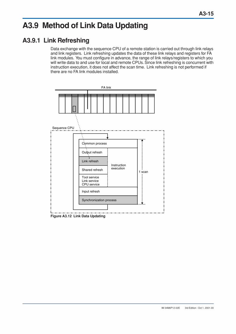
A3-15
IM 34M6P12-02E 3rd Edition : Oct 1, 2001-00
A3.9 Method of Link Data Updating
A3.9.1 Link RefreshingData exchange with the sequence CPU of a remote station is carried out through link relaysand link registers. Link refreshing updates the data of these link relays and registers for FAlink modules. You must configure in advance, the range of link relays/registers to which youwill write data to and use for local and remote CPUs. Since link refreshing is concurrent withinstruction execution, it does not affect the scan time. Link refreshing is not performed ifthere are no FA link modules installed.
Common process
Output refresh
Input refresh
Synchronization process
Instructionexecution
Link refresh
Shared refresh
Tool serviceLink serviceCPU service
1 scan
Sequence CPU
FA link
Figure A3.12 Link Data Updating
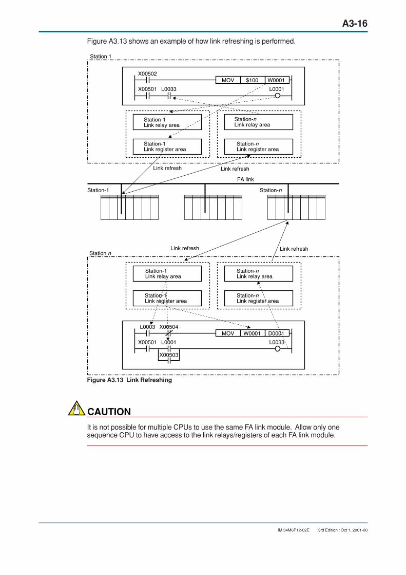
A3-16
IM 34M6P12-02E 3rd Edition : Oct 1, 2001-00
Figure A3.13 shows an example of how link refreshing is performed.
L0003 X00504
X00501 L0001
X00503
L0033
X00502
X00501 L0033 L0001
MOV $100 W0001
MOV W0001 D0001
Station-1Link relay area
Station-1Link register area
Station-nLink relay area
Station-nLink register area
Station-1Link relay area
Station-1Link register area
Station-nLink relay area
Station-nLink register area
Link refresh
Link refresh Link refresh
Station n
Station 1
Station-1 Station-n
FA link
Link refresh
Figure A3.13 Link Refreshing
CAUTION
It is not possible for multiple CPUs to use the same FA link module. Allow only onesequence CPU to have access to the link relays/registers of each FA link module.
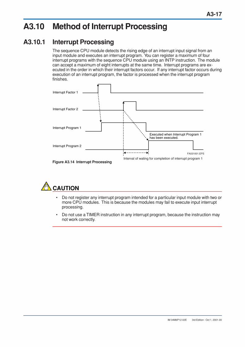
A3-17
IM 34M6P12-02E 3rd Edition : Oct 1, 2001-00
A3.10 Method of Interrupt Processing
A3.10.1 Interrupt ProcessingThe sequence CPU module detects the rising edge of an interrupt input signal from aninput module and executes an interrupt program. You can register a maximum of fourinterrupt programs with the sequence CPU module using an INTP instruction. The modulecan accept a maximum of eight interrupts at the same time. Interrupt programs are ex-ecuted in the order in which their interrupt factors occur. If any interrupt factor occurs duringexecution of an interrupt program, the factor is processed when the interrupt programfinishes.
Interrupt Factor 1
Interrupt Factor 2
Interrupt Program 1
Interrupt Program 2
Executed when Interrupt Program 1has been executed.
FA031001.EPS
Interval of wating for completion of interrupt program 1Figure A3.14 Interrupt Processing
CAUTION
• Do not register any interrupt program intended for a particular input module with two ormore CPU modules. This is because the modules may fail to execute input interruptprocessing.
• Do not use a TIMER instruction in any interrupt program, because the instruction maynot work correctly.

A3-18
IM 34M6P12-02E 3rd Edition : Oct 1, 2001-00
A3.10.2 Interrupt Processing ControlYou can control your execution of interrupt programs by means of programming. Use EIand DI instructions to determine whether the interrupt program in question is "executed"(cancellation of interrupt prohibition) or "not executed" (prohibition of interrupt). The defaultis the "Executed" option. Although the sequence CPU recognizes any interrupt occurring ina case where you have selected the "Not executed" option with a DI instruction, it does notexecute the relevant interrupt program.
Such interrupts are processed in order of their occurrence, after you have selected the"Executed" option with an EI instruction.
A maximum of eight interrupts are accepted at the same time. Simultaneous input of nineor more interrupts results in an interrupt error.
X00503 I0002 Y00603
X00501 X00502
I0003
I0004
I0005
I0001 Y00602
X00501DI
EI
IRET
X00301INTP
The interrupt programis not executed in thisperiod.
An interruptoccurs.
FA031002.EPS
Figure A3.15 Interrupt Processing Control
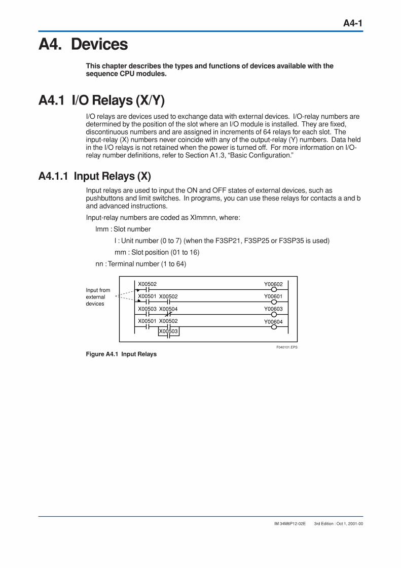
A4-1
IM 34M6P12-02E 3rd Edition : Oct 1, 2001-00
A4. DevicesThis chapter describes the types and functions of devices available with thesequence CPU modules.
A4.1 I/O Relays (X/Y)I/O relays are devices used to exchange data with external devices. I/O-relay numbers aredetermined by the position of the slot where an I/O module is installed. They are fixed,discontinuous numbers and are assigned in increments of 64 relays for each slot. Theinput-relay (X) numbers never coincide with any of the output-relay (Y) numbers. Data heldin the I/O relays is not retained when the power is turned off. For more information on I/O-relay number definitions, refer to Section A1.3, “Basic Configuration.”
A4.1.1 Input Relays (X)Input relays are used to input the ON and OFF states of external devices, such aspushbuttons and limit switches. In programs, you can use these relays for contacts a and band advanced instructions.
Input-relay numbers are coded as Xlmmnn, where:
lmm : Slot number
l : Unit number (0 to 7) (when the F3SP21, F3SP25 or F3SP35 is used)
mm : Slot position (01 to 16)
nn : Terminal number (1 to 64)
X00503 Y00603
X00501 X00502
X00504
X00502
X00503
Y00602
Y00601
Y00604
X00501
X00502Input fromexternaldevices
F040101.EPS
Figure A4.1 Input Relays
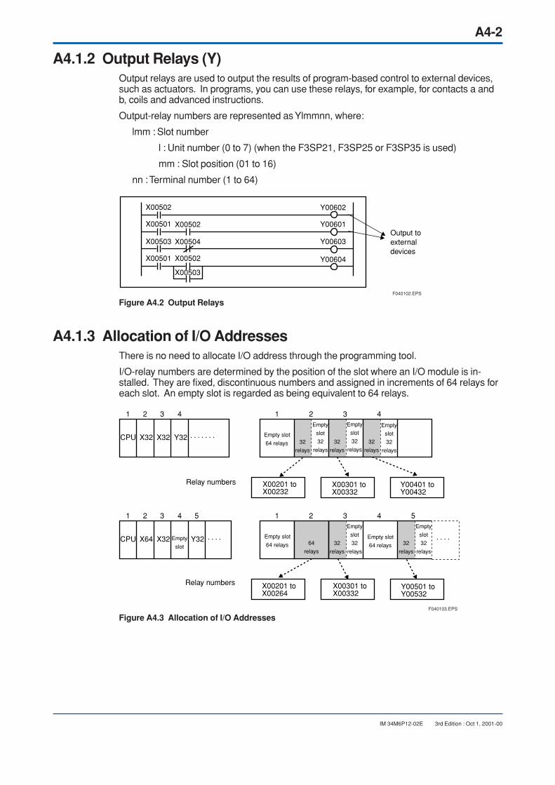
A4-2
IM 34M6P12-02E 3rd Edition : Oct 1, 2001-00
A4.1.2 Output Relays (Y)Output relays are used to output the results of program-based control to external devices,such as actuators. In programs, you can use these relays, for example, for contacts a andb, coils and advanced instructions.
Output-relay numbers are represented as Ylmmnn, where:
lmm : Slot number
l : Unit number (0 to 7) (when the F3SP21, F3SP25 or F3SP35 is used)
mm : Slot position (01 to 16)
nn : Terminal number (1 to 64)
X00503 Y00603
X00501 X00502
X00504
X00502
X00503
Y00602
Y00601
Y00604
X00501
X00502
Output toexternaldevices
F040102.EPS
Figure A4.2 Output Relays
A4.1.3 Allocation of I/O AddressesThere is no need to allocate I/O address through the programming tool.
I/O-relay numbers are determined by the position of the slot where an I/O module is in-stalled. They are fixed, discontinuous numbers and assigned in increments of 64 relays foreach slot. An empty slot is regarded as being equivalent to 64 relays.
CPU X32 X32 Y32
14321 2 3 4
CPU X64 X32 Y32
14 5321 2 3 4 5
Empty slot
64 relays
Empty slot
64 relaysEmpty slot
64 relays
32
relays
32
relays
32
relays
32
relays
32
relays
Empty
slot
32
relays
Empty
slot
32
relays
Empty
slot
32
relays
Empty
slot
32
relays
Empty
slot
32
relays
Relay numbers X00201 toX00232
X00301 toX00332
Y00401 toY00432
Empty
slot64
relays
Relay numbers X00201 toX00264
X00301 toX00332
Y00501 toY00532
F040103.EPS
Figure A4.3 Allocation of I/O Addresses
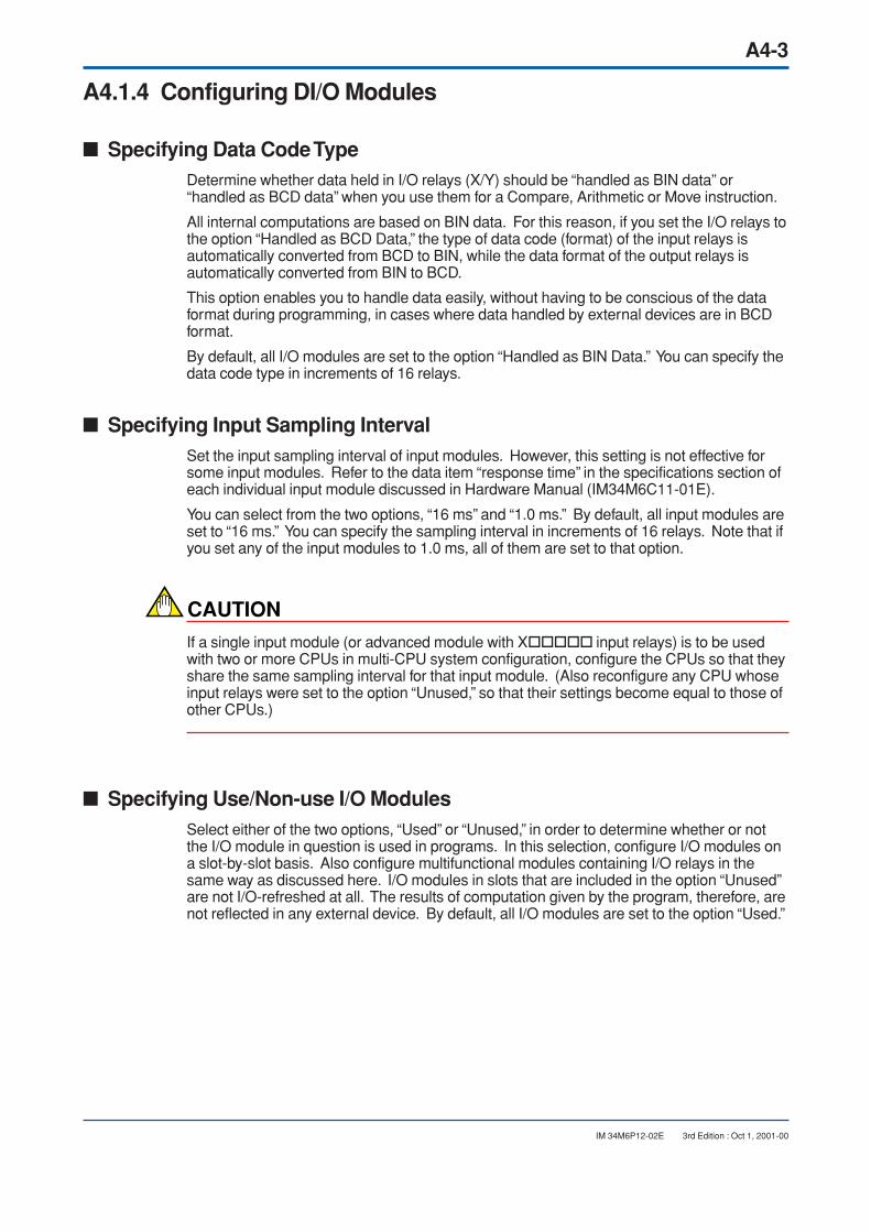
A4-3
IM 34M6P12-02E 3rd Edition : Oct 1, 2001-00
A4.1.4 Configuring DI/O Modules
Specifying Data Code TypeDetermine whether data held in I/O relays (X/Y) should be “handled as BIN data” or“handled as BCD data” when you use them for a Compare, Arithmetic or Move instruction.
All internal computations are based on BIN data. For this reason, if you set the I/O relays tothe option “Handled as BCD Data,” the type of data code (format) of the input relays isautomatically converted from BCD to BIN, while the data format of the output relays isautomatically converted from BIN to BCD.
This option enables you to handle data easily, without having to be conscious of the dataformat during programming, in cases where data handled by external devices are in BCDformat.
By default, all I/O modules are set to the option “Handled as BIN Data.” You can specify thedata code type in increments of 16 relays.
Specifying Input Sampling IntervalSet the input sampling interval of input modules. However, this setting is not effective forsome input modules. Refer to the data item “response time” in the specifications section ofeach individual input module discussed in Hardware Manual (IM34M6C11-01E).
You can select from the two options, “16 ms” and “1.0 ms.” By default, all input modules areset to “16 ms.” You can specify the sampling interval in increments of 16 relays. Note that ifyou set any of the input modules to 1.0 ms, all of them are set to that option.
CAUTION
If a single input module (or advanced module with X input relays) is to be usedwith two or more CPUs in multi-CPU system configuration, configure the CPUs so that theyshare the same sampling interval for that input module. (Also reconfigure any CPU whoseinput relays were set to the option “Unused,” so that their settings become equal to those ofother CPUs.)
Specifying Use/Non-use I/O ModulesSelect either of the two options, “Used” or “Unused,” in order to determine whether or notthe I/O module in question is used in programs. In this selection, configure I/O modules ona slot-by-slot basis. Also configure multifunctional modules containing I/O relays in thesame way as discussed here. I/O modules in slots that are included in the option “Unused”are not I/O-refreshed at all. The results of computation given by the program, therefore, arenot reflected in any external device. By default, all I/O modules are set to the option “Used.”

A4-4
IM 34M6P12-02E 3rd Edition : Oct 1, 2001-00
Holding/Resetting Output Relays When a Program StopsDetermine whether the output relays of an output module (or multifunctional module withoutput relays Y) should be placed in a “Hold” state or “Reset” state when a pro-gram stops (due to a moderate or major failure or a change to stop mode). The setting ofthis configuration for a stop of programs due to a major failure is not effective for someoutput modules, however. Refer to the data item “output in case of stop of programs” in thespecifications section of each individual output module discussed in Hardware Manual(IM34M6C11-01E).
For a multifunctional module, the setting for a stop of programs due to a major failure isalways set to ineffective.
By default, all output modules are set to the option “Reset.” You can perform this configura-tion in increments of 16 relays.
CAUTION
If a single output module (or advanced module with X output relays) is to be usedby two or more CPUs in multi-CPU system configuration, configure the CPUs so that all ofthem share the same output mode, either the “Hold” or “Reset” option. (Also reconfigureany CPU whose output relays were set to the option “Unused,” so that their settings be-come equal to those of remote CPUs.)

A4-5
IM 34M6P12-02E 3rd Edition : Oct 1, 2001-00
A4.2 Internal Relays (I), Shared Relays (E) andExtended Shared Relays (E)
A4.2.1 Internal Relays (I)Internal relays are auxiliary relays available for programs.
In programs, you can use these relays, for example, for contacts a and b, coils and ad-vanced instructions. Unlike I/O relays however, these relays cannot directly exchangesignals with an external device. There is no limitation on the number of contacts a and bthat can be used in a program.
X00503 Y00603
X00501 X00502
I0002
X00502
I0003
Y00602
I0003
I0004
X00501
I0001
F040201.EPS
Figure A4.4 Internal Relays
With the configuration function, you can configure a range of internal relays to determinewhether or not they retain computation results when the power is turned off. If you set theinternal relays so as not to retain computation results, they are cleared to “OFF (0)” whenyou:
• turn off the power once and turn it on again;
• change the operation mode to Run or Debug with the programming tool; or
• send a device clearance command from the programming tool.
If you set the internal relays so as to retain computation results, the latest data is retainedafter power-off. In this case, the relays are cleared to “OFF (0)” when you send a deviceclearance command from the programming tool.
A4-6
IM 34M6P12-02E 3rd Edition : Oct 1, 2001-00
A4.2.2 Shared Relays (E) and Extended Shared Relays (E)Shared and extended shared relays are used to perform CPU-to-CPU communication incases where a sequence CPU and add-on CPUs are installed.
The shared relays are available irrespective of how the sequence CPU is combined withthe add-on CPUs. The extended shared relays are available only if the F3SP25 or F3SP35sequence CPU is combined with another one or more F3SP25 or F3SP35 sequence CPUsinstalled as add-on CPUs.
In programs, you can use these relays, for example, for contacts a and b, coils and ad-vanced instructions. In addition, you can exchange ON/OFF data between CPUs by usingshared relays of the local CPU as coils and those of the remote CPUs as contacts.
CAUTION
If you write data to a device area other than that of the local CPU, information held byshared and extended shared relays of remote CPUs are overwritten. This results in afailure for these shared relays to reflect the correct results of computation.
By default, no shared relays are assigned as devices. When using shared relays, set theirrange by means of the configuration function. Assign the same range for all of the CPUs.Otherwise, the shared relays are not correctly refreshed.
Note that advanced instructions that contain any extended shared relays are excluded fromhigh-speed processing.
SEE ALSO
Section 1.7, “High speed Processing of Application Instructions,” Sequence CPUInstruction Manual - Instructions (IM34M6P12-03E), for details on the high-speed process-ing of application instructions.

A4-7
IM 34M6P12-02E 3rd Edition : Oct 1, 2001-00
Figure A4.5 shows an example of how specific shared relays are shared if you allocateshared relays E0001-0512 to CPU1 and E0513-1024 to CPU2.
X00503 Y00603
X00501 X00502
E0010
X00502
I0003
E0010
I0003
E0513
E0513
I0001
CPU I
CPU 2
F040202.EPS
Figure A4.5 Shared Relays
With the configuration function, you can configure a range of shared relays to determinewhether or not they retain computation results when the power is turned off. By default, allshared relays are set so as not to retain computation results. If you set the shared relays tothis option, they are cleared to “OFF (0)” when you:
• turn off the power and turn it on again;
• change the operation mode to Run or Debug with the programming tool; or
• send a device clearance command from the programming tool.
If you set the shared relays so as to retain computation results, the latest results are re-tained after power-off. In this case, the relays are cleared to “OFF (0)” when you send adevice clearance command from the programming tool.
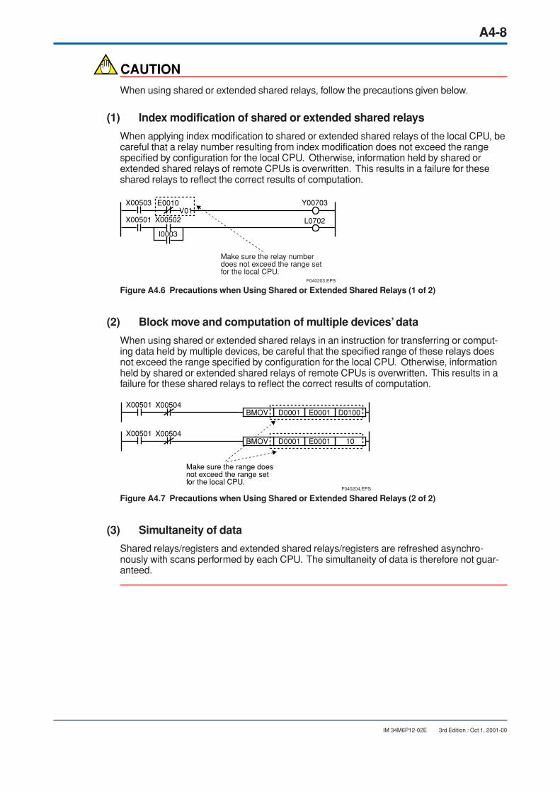
A4-8
IM 34M6P12-02E 3rd Edition : Oct 1, 2001-00
CAUTION
When using shared or extended shared relays, follow the precautions given below.
(1) Index modification of shared or extended shared relays
When applying index modification to shared or extended shared relays of the local CPU, becareful that a relay number resulting from index modification does not exceed the rangespecified by configuration for the local CPU. Otherwise, information held by shared orextended shared relays of remote CPUs is overwritten. This results in a failure for theseshared relays to reflect the correct results of computation.
X00503 Y00703
X00501 X00502
E0010
I0003
L0702V01
Make sure the relay numberdoes not exceed the range setfor the local CPU.
F040203.EPS
Figure A4.6 Precautions when Using Shared or Extended Shared Relays (1 of 2)
(2) Block move and computation of multiple devices’ data
When using shared or extended shared relays in an instruction for transferring or comput-ing data held by multiple devices, be careful that the specified range of these relays doesnot exceed the range specified by configuration for the local CPU. Otherwise, informationheld by shared or extended shared relays of remote CPUs is overwritten. This results in afailure for these shared relays to reflect the correct results of computation.
X00501 X00504E0001D0001BMOV D0100
X00501 X00504E0001D0001BMOV 10
Make sure the range doesnot exceed the range setfor the local CPU.
F040204.EPS
Figure A4.7 Precautions when Using Shared or Extended Shared Relays (2 of 2)
(3) Simultaneity of data
Shared relays/registers and extended shared relays/registers are refreshed asynchro-nously with scans performed by each CPU. The simultaneity of data is therefore not guar-anteed.

A4-9
IM 34M6P12-02E 3rd Edition : Oct 1, 2001-00
A4.2.3 Configuring Internal Relays (I), Shared Relays (E) andExtended Shared Relays (E)
Set the range of internal, shared and extended shared relays to be used. This configurationis necessary when an add-on CPU or CPUs are installed. Ranges are assigned to thesedevices in the order of internal relays and then shared relays and on 32 points basis.
Table A4.1 Configuration of Internal and Shared Relays (for F3SP21, F3SP25 and F3SP35)
ItemF3SP25 F3SP35
Default DefaultConfiguration Range Configuration RangeF3SP21
Default
I0001 to I8192
I0001 to I4096
–
– – – –
– –
I0001 to 16384
Configuration Range
4096 points max. on 32 points basis for all internal and shared relays combinedInternal relay numbers: I0001 to I4096Shared relay numbers: E0001 to E2048
16384 points max. on 32 points basis for all internal and shared relays combinedInternal relay numbers: I00001 to I16384Shared relay numbers: E0001 to E2048
8192 points max. on 32 points basis for all internal and shared relays combinedInternal relay numbers: I0001 to I8192Shared relay numbers: E0001 to E2048
Configurable on 32 points basis for relay numbers from E2049 to E4096
Configurable in on 32 points basis for relay numbers from E2049 to E4096
Internal relay (I)
Shared relay (E)
Extendedshared relay (E)
TA040201.EPS
CAUTION
The starting number of extended shared relays is always E2049, even if the range ofshared relays to be used is less than 2048.
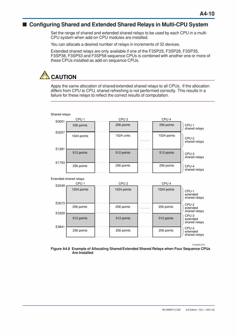
A4-10
IM 34M6P12-02E 3rd Edition : Oct 1, 2001-00
Configuring Shared and Extended Shared Relays in Multi-CPU SystemSet the range of shared and extended shared relays to be used by each CPU in a multi-CPU system when add-on CPU modules are installed.
You can allocate a desired number of relays in increments of 32 devices.
Extended shared relays are only available if one of the F3SP25, F3SP28, F3SP35,F3SP38, F3SP53 and F3SP58 sequence CPUs is combined with another one or more ofthese CPUs installed as add-on sequence CPUs.
CAUTION
Apply the same allocation of shared/extended shared relays to all CPUs. If the allocationdiffers from CPU to CPU, shared refreshing is not performed correctly. This results in afailure for these relays to reflect the correct results of computation.
Shared relays
E0001
E0257
E1281
E1793
Extended shared relays
256 points
1024 points
512 points
256 points
CPU-1 shared relays
CPU-2shared relays
CPU-3shared relays
CPU-4shared relays
CPU 1 CPU 2 CPU 4
E2049
E3073
E3329
E3841
1024 points
256 points
512 points
256 points
CPU-1extendedshared relays
CPU-2extendedshared relays
CPU-3extendedshared relays
CPU-4extendedshared relays
CPU 1 CPU 2 CPU 4
F040205.EPS
256 points
1024 units
512 points
256 points
256 points
1024 points
512 points
256 points
1024 points
256 points
512 points
256 points
1024 points
256 points
512 points
256 points
Figure A4.8 Example of Allocating Shared/Extended Shared Relays when Four Sequence CPUs Are Installed
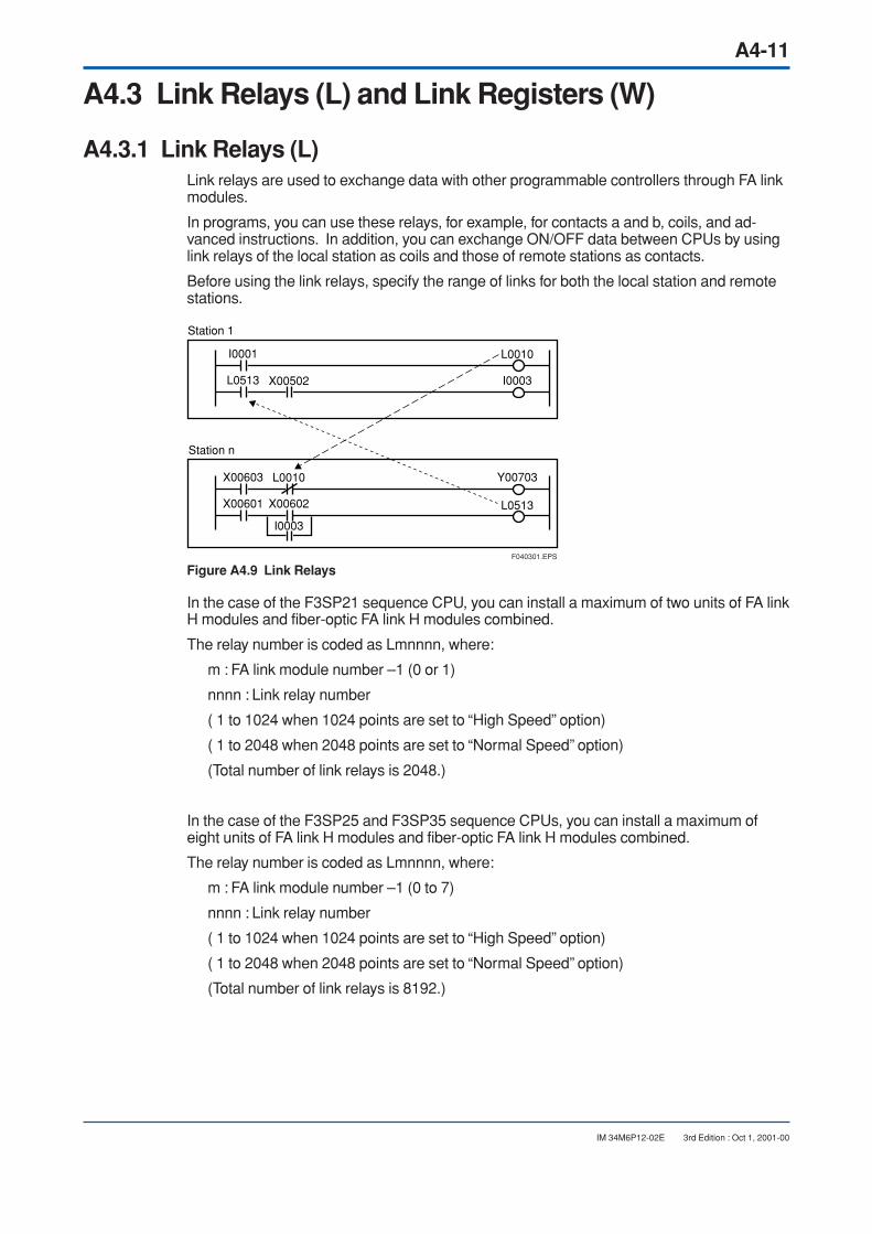
A4-11
IM 34M6P12-02E 3rd Edition : Oct 1, 2001-00
A4.3 Link Relays (L) and Link Registers (W)
A4.3.1 Link Relays (L)Link relays are used to exchange data with other programmable controllers through FA linkmodules.
In programs, you can use these relays, for example, for contacts a and b, coils, and ad-vanced instructions. In addition, you can exchange ON/OFF data between CPUs by usinglink relays of the local station as coils and those of remote stations as contacts.
Before using the link relays, specify the range of links for both the local station and remotestations.
X00603 Y00703
X00601 X00602
L0010
X00502
I0003
L0010
I0003
L0513
L0513
I0001
Station 1
Station n
F040301.EPS
Figure A4.9 Link Relays
In the case of the F3SP21 sequence CPU, you can install a maximum of two units of FA linkH modules and fiber-optic FA link H modules combined.
The relay number is coded as Lmnnnn, where:
m : FA link module number –1 (0 or 1)
nnnn : Link relay number
( 1 to 1024 when 1024 points are set to “High Speed” option)
( 1 to 2048 when 2048 points are set to “Normal Speed” option)
(Total number of link relays is 2048.)
In the case of the F3SP25 and F3SP35 sequence CPUs, you can install a maximum ofeight units of FA link H modules and fiber-optic FA link H modules combined.
The relay number is coded as Lmnnnn, where:
m : FA link module number –1 (0 to 7)
nnnn : Link relay number
( 1 to 1024 when 1024 points are set to “High Speed” option)
( 1 to 2048 when 2048 points are set to “Normal Speed” option)
(Total number of link relays is 8192.)

A4-12
IM 34M6P12-02E 3rd Edition : Oct 1, 2001-00
CAUTION
• Use the FA link H module and/or fiber-optic FA link H module only in combination withthe R1.08 or later version of Ladder Diagram Support Program M3 and with the Rev.8or later version of the F3SP21, F3SP25 and F3SP35.
• For each of the F3LP02 FA link H module and F3LP12 fiber-optic FA link H module,you can use a maximum of 2048 units of link relays and link registers. The configura-tion limitations described below apply, however, if a single CPU uses a combination offiber-optic FA link H modules configured with 1024 units of link relays/registers set forhigh-speed processing and fiber-optic FA link H modules configured with 2048 units oflink relays/registers set for normal-speed processing.
Configuration limitations:
For FA link 1, be sure to set the number of both link relays and link registers to 2048. If youset the number to 1024, the CPU does not operate correctly. If the number of both linkrelays and link registers is set to 0 for FA link 1, be sure to set the number to 2048 for FAlink 2.
Examples of Unallowable Configuration:
Link 1: [1024]; Link 2: [2048]; Link 3: . . .
Link 1: [ 0]; Link 2: [1024]; Link 3: [2048]; . . .
Link 1: [1024]; Link 2: [ 0]; Link 3: [2048]; . . .
Examples of Allowable Configuration:
Link 1: [2048]; Link 2: . . .
Link 1: [1024]; Link 2: [1024]; Link 3: . . .
Link 1: [ 0]; Link 2: [1024]; Link 3: [1024]; . . .
Link 1: [1024]; Link 2: [ 0]; Link 3: [1024]; . . .
Link 1: [ 0]; Link 2: [2048]; Link 3: . . .
TIP
FA link module (line) numbers are in one-to-one relationship with the FA link modulesinstalled. The FA link modules are numbered 1, 2, and so on, in ascending order of thenumbers assigned to the slots where the modules are installed. Their link relays are num-bered L00001 to L01024 (or L02048), L10001 to L11024 (or L12048), and so on.
With the configuration function, you can newly correlate a slot number with each FA linkmodule number for a slot where the FA link module is installed. The following illustrationshows an example of this configuration, as well as the relationship between the slot num-bers and link relay numbers.
As shown in the example, this configuration allows you to use the same numbering format,such as L1nnnn, to encode link relay numbers at each station within a given FA link. Inaddition, you need not change the link relay numbers when you install an additional FA linkmodule.
Even if there are no FA link modules installed, you can specify a maximum of two FA linkmodule numbers for the F3SP21 sequence CPU module and a maximum of eight FA linkmodule numbers for the F3SP25/F3SP35 sequence CPU modules.
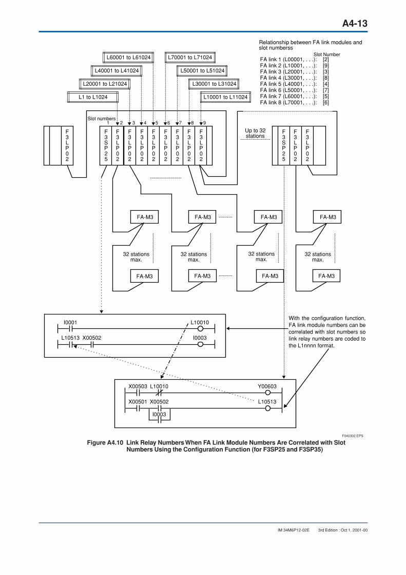
A4-13
IM 34M6P12-02E 3rd Edition : Oct 1, 2001-00
I0001 L10010
L10513 X00502 I0003
X00503 L10010 Y00603
X00501 X00502
I0003
L10513
L60001 to L61024 L70001 to L71024
L40001 to L41024 L50001 to L51024
L20001 to L21024 L30001 to L31024
L1 to L1024 L10001 to L11024
FA-M3
FA-M3
FA-M3 FA-M3 FA-M3
FA-M3 FA-M3 FA-M3
Relationship between FA link modules andslot numberss
Slot Number
Slot numbers
FA link 1 (L00001, . . .): [2]FA link 2 (L10001, . . .): [9]FA link 3 (L20001, . . .): [3]FA link 4 (L30001, . . .): [8]FA link 5 (L40001, . . .): [4]FA link 6 (L50001, . . .): [7]FA link 7 (L60001, . . .): [5]FA link 8 (L70001, . . .): [6]
Up to 32stations
With the configuration function, FA link module numbers can be correlated with slot numbers so link relay numbers are coded to the L1nnnn format.
1 2 3 4 5 6 7 8 9
F3SP25
32 stationsmax.
32 stationsmax.
32 stationsmax.
32 stationsmax.
F040302.EPS
F3LP02
F3LP02
F3LP02
F3LP02
F3LP02
F3LP02
F3LP02
F3LP02
F3LP02
F3SP25
F3LP02
F3LP02
Figure A4.10 Link Relay Numbers When FA Link Module Numbers Are Correlated with Slot Numbers Using the Configuration Function (for F3SP25 and F3SP35)

A4-14
IM 34M6P12-02E 3rd Edition : Oct 1, 2001-00
With the configuration function, you can determine whether or not link relays retain compu-tation results when the power is turned off. By default, all link relays are set so as not toretain computation results. If you set the link relays to this option, they are cleared to OFF(0) when you:
• turn off the power and turn it on again;
• change the operation mode to Run or Debug with the programming tool; or
• send a device clearance command from the programming tool.
If you set the link relays so as to retain computation results, the latest results are retainedafter power-off. In this case, the relays are cleared to “OFF (0)” when you send a deviceclearance command from the programming tool.
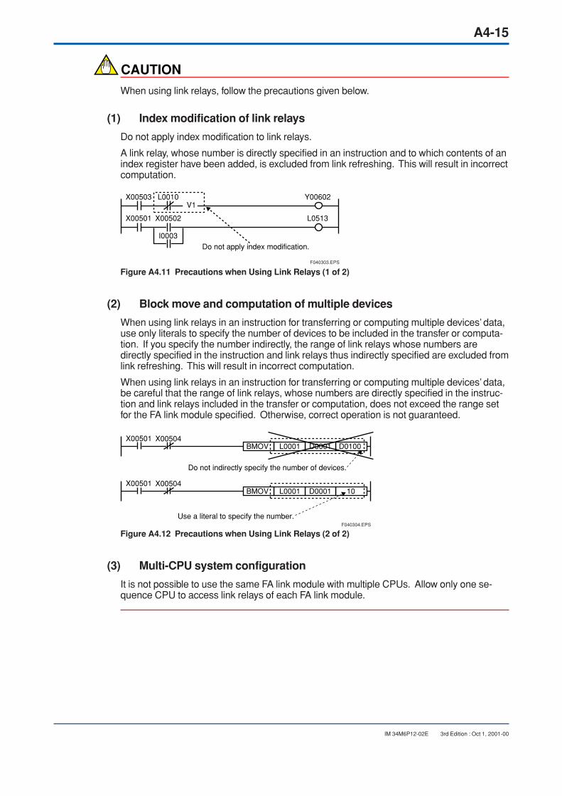
A4-15
IM 34M6P12-02E 3rd Edition : Oct 1, 2001-00
CAUTION
When using link relays, follow the precautions given below.
(1) Index modification of link relays
Do not apply index modification to link relays.
A link relay, whose number is directly specified in an instruction and to which contents of anindex register have been added, is excluded from link refreshing. This will result in incorrectcomputation.
X00503 L0010 Y00602
X00501 X00502
I0003
L0513
V1
Do not apply index modification.
F040303.EPS
Figure A4.11 Precautions when Using Link Relays (1 of 2)
(2) Block move and computation of multiple devices
When using link relays in an instruction for transferring or computing multiple devices’ data,use only literals to specify the number of devices to be included in the transfer or computa-tion. If you specify the number indirectly, the range of link relays whose numbers aredirectly specified in the instruction and link relays thus indirectly specified are excluded fromlink refreshing. This will result in incorrect computation.
When using link relays in an instruction for transferring or computing multiple devices’ data,be careful that the range of link relays, whose numbers are directly specified in the instruc-tion and link relays included in the transfer or computation, does not exceed the range setfor the FA link module specified. Otherwise, correct operation is not guaranteed.
X00501 X00504D0001L0001BMOV D0100
X00501 X00504D0001L0001BMOV 10
Do not indirectly specify the number of devices.
Use a literal to specify the number.F040304.EPS
Figure A4.12 Precautions when Using Link Relays (2 of 2)
(3) Multi-CPU system configuration
It is not possible to use the same FA link module with multiple CPUs. Allow only one se-quence CPU to access link relays of each FA link module.
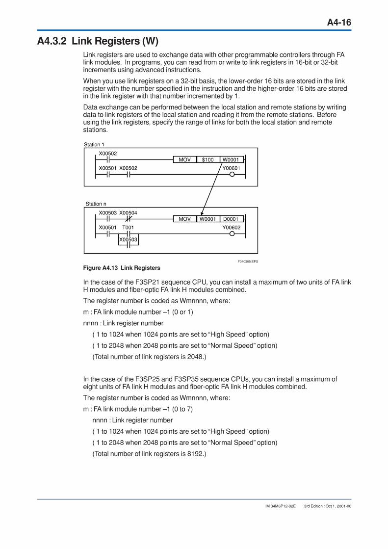
A4-16
IM 34M6P12-02E 3rd Edition : Oct 1, 2001-00
A4.3.2 Link Registers (W)Link registers are used to exchange data with other programmable controllers through FAlink modules. In programs, you can read from or write to link registers in 16-bit or 32-bitincrements using advanced instructions.
When you use link registers on a 32-bit basis, the lower-order 16 bits are stored in the linkregister with the number specified in the instruction and the higher-order 16 bits are storedin the link register with that number incremented by 1.
Data exchange can be performed between the local station and remote stations by writingdata to link registers of the local station and reading it from the remote stations. Beforeusing the link registers, specify the range of links for both the local station and remotestations.
X00503 X00504
X00501 T001
X00503
Y00602
MOV W0001 D0001
X00502
X00501 X00502 Y00601
MOV $100 W0001
Station 1
Station n
F040305.EPS
Figure A4.13 Link Registers
In the case of the F3SP21 sequence CPU, you can install a maximum of two units of FA linkH modules and fiber-optic FA link H modules combined.
The register number is coded as Wmnnnn, where:
m : FA link module number –1 (0 or 1)
nnnn : Link register number
( 1 to 1024 when 1024 points are set to “High Speed” option)
( 1 to 2048 when 2048 points are set to “Normal Speed” option)
(Total number of link registers is 2048.)
In the case of the F3SP25 and F3SP35 sequence CPUs, you can install a maximum ofeight units of FA link H modules and fiber-optic FA link H modules combined.
The register number is coded as Wmnnnn, where:
m : FA link module number –1 (0 to 7)
nnnn : Link register number
( 1 to 1024 when 1024 points are set to “High Speed” option)
( 1 to 2048 when 2048 points are set to “Normal Speed” option)
(Total number of link registers is 8192.)

A4-17
IM 34M6P12-02E 3rd Edition : Oct 1, 2001-00
CAUTION
• Use the FA link H module and/or fiber-optic FA link H module only in combination withthe R1.08 or later version of Ladder Diagram Support Program M3 and with the Rev.8or later version of the F3SP21, F3SP25 and F3SP35.
• For each of the F3LP02 FA link H module and F3LP12 fiber-optic FA link H module,you can use a maximum of 2048 units of link relays and link registers. The configura-tion limitations described below apply, however, if a single CPU uses a combination ofFA link H or fiber-optic FA link H modules configured with 1024 units of link relays/registers set for high-speed processing and FA link H or fiber-optic FA link H modulesconfigured with 2048 units of link relays/registers set for normal-speed processing.
Configuration limitations:
For FA link 1, be sure to set the number of both link relays and link registers to 2048. If youset the number to 1024, the CPU does not operate correctly. If the number of both linkrelays and link registers is set to 0 for FA link 1, be sure to set the number to 2048 for FAlink 2.
Examples of Unallowable Configuration:
Link 1: [1024]; Link 2: [2048]; Link 3: . . .
Link 1: [ 0]; Link 2: [1024]; Link 3: [2048]; . . .
Link 1: [1024]; Link 2: [ 0]; Link 3: [2048]; . . .
Examples of Allowable Configuration:
Link 1: [2048]; Link 2: . . .
Link 1: [1024]; Link 2: [1024]; Link 3: . . .
Link 1: [ 0]; Link 2: [1024]; Link 3: [1024]; . . .
Link 1: [1024]; Link 2: [ 0]; Link 3: [1024]; . . .
Link 1: [ 0]; Link 2: [2048]; Link 3: . . .
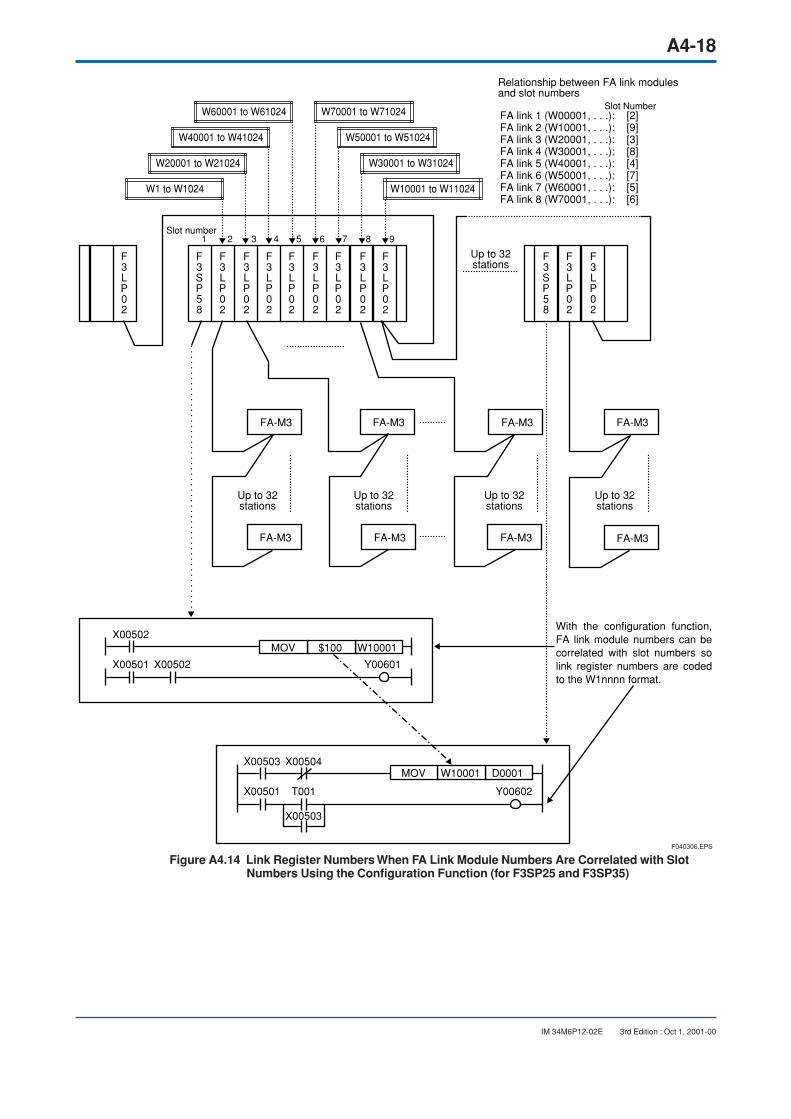
A4-18
IM 34M6P12-02E 3rd Edition : Oct 1, 2001-00
X00502
X00501 X00502 Y00601
X00503 X00504
X00501 T001
X00503
Y00602
W60001 to W61024 W70001 to W71024
W40001 to W41024 W50001 to W51024
W20001 to W21024 W30001 to W31024
W1 to W1024 W10001 to W11024
FA-M3 FA-M3 FA-M3 FA-M3
Relationship between FA link modulesand slot numbers
Slot Number
Slot number
FA link 1 (W00001, . . .): [2]FA link 2 (W10001, . . .): [9]FA link 3 (W20001, . . .): [3]FA link 4 (W30001, . . .): [8]FA link 5 (W40001, . . .): [4]FA link 6 (W50001, . . .): [7]FA link 7 (W60001, . . .): [5]FA link 8 (W70001, . . .): [6]
Up to 32stations
With the configuration function, FA link module numbers can be correlated with slot numbers so link register numbers are coded to the W1nnnn format.
1 2 3 4 5 6 7 8 9
Up to 32stations
Up to 32stations
Up to 32stations
Up to 32stations
MOV W10001 D0001
MOV $100 W10001
F040306.EPS
F3SP58
F3LP02
F3LP02
F3LP02
F3LP02
F3LP02
F3LP02
F3LP02
F3LP02
F3SP58
F3LP02
F3LP02
F3LP02
FA-M3 FA-M3 FA-M3 FA-M3
Figure A4.14 Link Register Numbers When FA Link Module Numbers Are Correlated with Slot Numbers Using the Configuration Function (for F3SP25 and F3SP35)

A4-19
IM 34M6P12-02E 3rd Edition : Oct 1, 2001-00
With the configuration function, you can determine whether or not link registers retaincomputation results when the power is turned off. By default, all link registers are set so asnot to retain computation results. If you set the link registers to this option, they are clearedwhen you:
• turn off the power and turn it on again;
• change the operation mode to Run or Debug with the programming tool; or
• send a device clearance command from the programming tool.
If you set the link registers so as to retain computation results, the latest results are retainedafter power-off. In this case, the registers are cleared when you send a device clearancecommand from the programming tool.

A4-20
IM 34M6P12-02E 3rd Edition : Oct 1, 2001-00
CAUTION
When using link registers, follow the precautions given below.
(1) Index modification of link registers
Do not apply index modification to link registers.
A link register, whose number is directly specified in an instruction and to which contents ofan index register have been added, is excluded from link refreshing. This will result inincorrect computation.
X00501
X00501 T001
I0003
Y00602
MOV W0001 B0001
V1
Do not apply index modification.F040307.EPS
Figure A4.15 Precautions when Using Link Registers (1 of 2)
(2) Block move and computation of multiple devices
When using link registers in an instruction for transferring or computing multiple devices’data, use only constants to specify the number of devices to be included in the transfer orcomputation. If you specify the number indirectly, the range of link registers whose num-bers are directly specified in the instruction and link registers thus indirectly specified, areexcluded from link refreshing. This will result in incorrect computation.
When using link registers in an instruction for transferring or computing multiple devices’data, be careful that the range of link registers, whose numbers are directly specified in theinstruction and link registers included in the transfer or computation, does not exceed therange set for the FA link module specified. Otherwise, correct operation is not guaranteed.
X00501 X00504D0001W0001BMOV D0100
X00501 X00504D0001W0001BMOV 10
Do not indirectly specify the number of devices.
Use a constant to specify the number.F040308.EPS
Figure A4.16 Precautions when Using Link Registers (2 of 2)
(3) Multi-CPU system configuration
It is not possible to use the same FA link module with multiple CPUs. Allow only one se-quence CPU to access link registers of each FA link module.
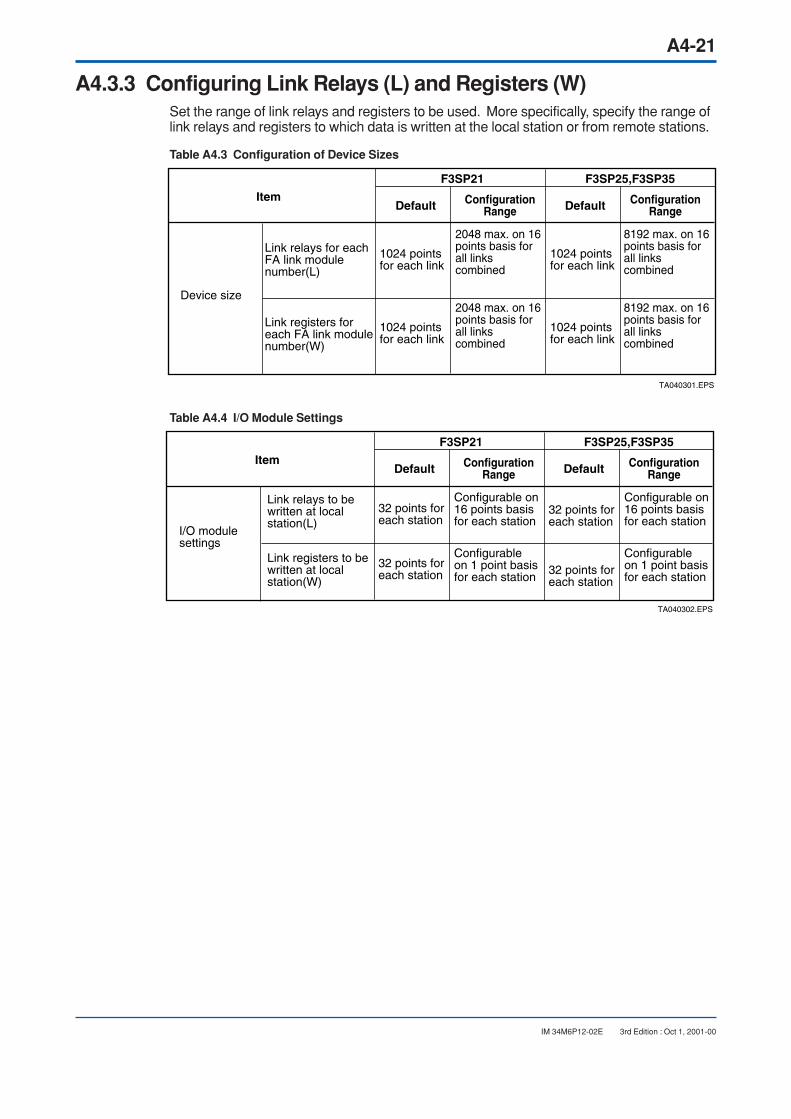
A4-21
IM 34M6P12-02E 3rd Edition : Oct 1, 2001-00
A4.3.3 Configuring Link Relays (L) and Registers (W)Set the range of link relays and registers to be used. More specifically, specify the range oflink relays and registers to which data is written at the local station or from remote stations.
Table A4.3 Configuration of Device Sizes
Item
F3SP25,F3SP35
Default
F3SP21
Default ConfigurationRange
ConfigurationRange
2048 max. on 16 points basis for all links combined
8192 max. on 16 points basis for all links combined
Link relays for eachFA link module number(L)
Link registers for each FA link module number(W)
Device size
TA040301.EPS
1024 pointsfor each link
1024 pointsfor each link
2048 max. on 16 points basis for all links combined
8192 max. on 16 points basis for all links combined
1024 pointsfor each link
1024 pointsfor each link
Table A4.4 I/O Module Settings
Item
F3SP25,F3SP35
Default
F3SP21
Default ConfigurationRange
ConfigurationRange
Configurable on 16 points basis for each station
Link relays to be written at local station(L)
Link registers to be written at local station(W)
I/O modulesettings
TA040302.EPS
32 points for each station
Configurable on 1 point basis for each station
Configurable on 1 point basis for each station
32 points for each station
Configurable on 16 points basis for each station
32 points for each station
32 points for each station

A4-22
IM 34M6P12-02E 3rd Edition : Oct 1, 2001-00
A4.4 Special Relays (M)Special relays have specific functions, such as indicating the internal state of a CPU ordetecting errors.
In programs, these relays are used mainly for contacts a and b.
A4.4.1 Block Start StatusBlock start status relays indicate which block is running when the selected blocks are beingexecuted.
These relays are numbered in ascending order as M001, M002, . . ., to correlate with block1, block 2, ...
Table A4.5 Block Start Status
Item Description
TA040401.EPS
CPU Module
F3SP21, F3SP25 and F3SP35 (Note)
Relay Number Name Function Remarks
M0001 to M0032Block n startstatus relay
ON : RunOFF: Stop
Indicate whether block n is in progress or at a stop when blocks are selected and executed.
Note: The start status relays assigned to blocks 1 to 32 are M0001 to M0032 and M2001 to M2032, where the values of M0001 to M0032 are the same as those of M2001 to M2032. Similarly, start status relays M2033 to M3024 are assigned to blocks 33 to 1024.
CAUTION
Do not write to a special relay, including those not listed in the table above (e.g., M067 toM128), unless otherwise stated. This is because they are used by the CPU module for thesystem. If you inadvertently write to these relays, a failure, such as a system shutdown,may result. (It is also prohibited to use a forced set/reset instruction in debug mode.)
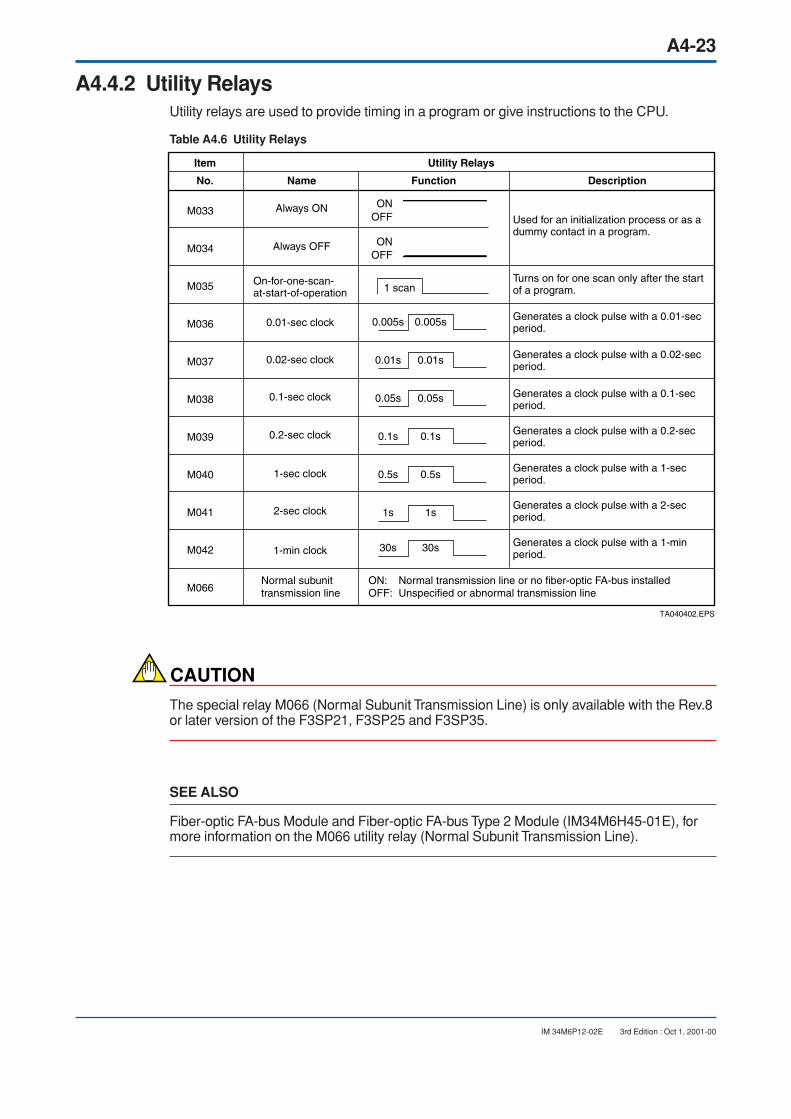
A4-23
IM 34M6P12-02E 3rd Edition : Oct 1, 2001-00
A4.4.2 Utility RelaysUtility relays are used to provide timing in a program or give instructions to the CPU.
Table A4.6 Utility Relays
Always ON
Always OFF
No.
Item Utility Relays
Name Function Description
On-for-one-scan-at-start-of-operation
M033
M034
M035
M036
M037
M038
M039
M040
M041
M042
M066
ONOFF
ONOFF
1 scan
0.005s0.005s
0.01s0.01s
0.05s0.05s
0.1s0.1s
0.5s0.5s
1s1s
30s30s
0.01-sec clock
0.02-sec clock
0.1-sec clock
0.2-sec clock
1-sec clock
2-sec clock
1-min clock
Used for an initialization process or as a dummy contact in a program.
Turns on for one scan only after the start of a program.
Generates a clock pulse with a 0.01-sec period.
Generates a clock pulse with a 0.02-sec period.
Generates a clock pulse with a 0.1-sec period.
TA040402.EPS
Generates a clock pulse with a 0.2-sec period.
Generates a clock pulse with a 1-sec period.
Generates a clock pulse with a 2-sec period.
Generates a clock pulse with a 1-min period.
Normal subunittransmission line
ON: Normal transmission line or no fiber-optic FA-bus installedOFF: Unspecified or abnormal transmission line
CAUTION
The special relay M066 (Normal Subunit Transmission Line) is only available with the Rev.8or later version of the F3SP21, F3SP25 and F3SP35.
SEE ALSO
Fiber-optic FA-bus Module and Fiber-optic FA-bus Type 2 Module (IM34M6H45-01E), formore information on the M066 utility relay (Normal Subunit Transmission Line).
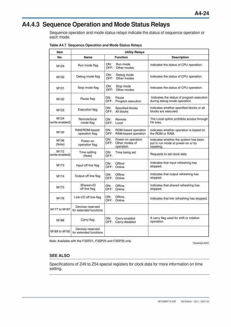
A4-24
IM 34M6P12-02E 3rd Edition : Oct 1, 2001-00
A4.4.3 Sequence Operation and Mode Status RelaysSequence operation and mode status relays indicate the status of sequence operation oreach mode.
Table A4.7 Sequence Operation and Mode Status Relays
Run mode flag
Debug mode flag
No.
Item Utility Relays
Name Function Description
Stop mode flag
M129
M130
M131
M132
M133
M134
M135
M136
M172
M173
M174
M175
M176
M177 to M187
M188
M189 to M192
Pause flag
Execution flag
Remote/localmode flag
RAM/ROM-based operation flag
Time setting(Note)
Input-off line flag
Output-off line flag
Shared-I/Ooff line flag
Link-I/O off line flag
Devices reservedfor extended functions
Devices reservedfor extended functions
Carry flag
Indicates the status of CPU operation.
Indicates the status of CPU operation.
Indicates the status of CPU operation.
Indicates the status of program execution during debug mode operation.
Indicates whether specified blocks or all blocks are executed.
The Local option prohibits access through FA links.
Indicates whether operation is based on the ROM or RAM.
Indicates that input refreshing has stopped.
Indicates that output refreshing has stopped.
Indicates that shared refreshing has stopped.
A carry flag used for shift or rotation operation.
Indicates that link refreshing has stopped.
Requests to set clock data
Indicates whether the system has been put in run mode at power-on or by resetting.
TA040403.EPS
Power-onoperation flag
(write-enabled)
(write-enabled)
(Note)
ON: Run modeOFF: Other modes
ON: Debug modeOFF: Other modes
ON: Stop modeOFF: Other modes
ON: PauseOFF: Program execution
ON: Specified blocksOFF: All blocks
ON: RemoteOFF: Local
ON: ROM-based operationOFF: RAM-based operation
ON: Power-on operationOFF: Other modes of
operation
ON: Time being setOFF:
ON: OfflineOFF: Online
ON: OfflineOFF: Online
ON: OfflineOFF: Online
ON: OfflineOFF: Online
ON: Carry-enabledOFF: Carry-disabled
Note: Available with the F3SP21, F3SP25 and F3SP35 only
SEE ALSO
Specifications of Z49 to Z54 special registers for clock data for more information on timesetting.
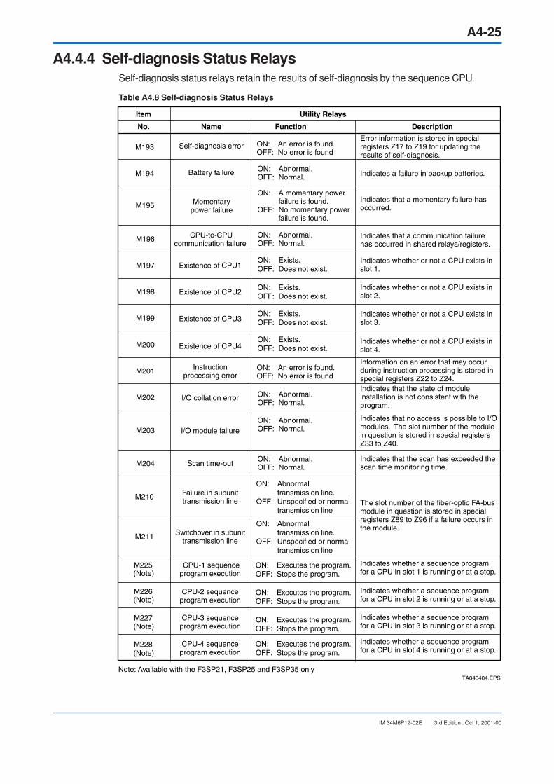
A4-25
IM 34M6P12-02E 3rd Edition : Oct 1, 2001-00
A4.4.4 Self-diagnosis Status RelaysSelf-diagnosis status relays retain the results of self-diagnosis by the sequence CPU.
Table A4.8 Self-diagnosis Status Relays
Self-diagnosis error
Battery failure
No.
Item Utility Relays
Name Function Description
Momentarypower failure
M193
M194
M196
M197
M198
M199
M200
M201
M202
M203
M204
CPU-to-CPUcommunication failure
Existence of CPU1
Existence of CPU2
Existence of CPU3
Instructionprocessing error
I/O collation error
I/O module failure
Scan time-out
Failure in subunittransmission line
Switchover in subunittransmission line
CPU-2 sequenceprogram execution
CPU-3 sequenceprogram execution
CPU-4 sequenceprogram execution
CPU-1 sequenceprogram execution
Error information is stored in special registers Z17 to Z19 for updating the results of self-diagnosis.
Indicates that a momentary failure has occurred.
Indicates that a communication failure has occurred in shared relays/registers.
Indicates a failure in backup batteries.
Indicates whether or not a CPU exists in slot 1.
Indicates whether or not a CPU exists in slot 2.
Indicates whether or not a CPU exists in slot 3.
Indicates that the state of module installation is not consistent with the program.
Indicates that no access is possible to I/O modules. The slot number of the module in question is stored in special registers Z33 to Z40.
Indicates that the scan has exceeded the scan time monitoring time.
Indicates whether a sequence program for a CPU in slot 1 is running or at a stop.
Indicates whether a sequence program for a CPU in slot 2 is running or at a stop.
Indicates whether a sequence program for a CPU in slot 3 is running or at a stop.
Indicates whether a sequence program for a CPU in slot 4 is running or at a stop.
The slot number of the fiber-optic FA-bus module in question is stored in special registers Z89 to Z96 if a failure occurs in the module.
Information on an error that may occur during instruction processing is stored in special registers Z22 to Z24.
Indicates whether or not a CPU exists in slot 4.
TA040404.EPS
Existence of CPU4
ON: An error is found.OFF: No error is found
ON: An error is found.OFF: No error is found
Note: Available with the F3SP21, F3SP25 and F3SP35 only
(Note)
(Note)
(Note)
(Note)
ON: Abnormal.OFF: Normal.
ON: Abnormal.OFF: Normal.
ON: Abnormal.OFF: Normal.
ON: Abnormal.OFF: Normal.
ON: Abnormal.OFF: Normal.
ON: A momentary powerfailure is found.
OFF: No momentary powerfailure is found.
ON: Exists.OFF: Does not exist.
ON: Exists.OFF: Does not exist.
ON: Exists.OFF: Does not exist.
ON: Exists.OFF: Does not exist.
ON: Abnormaltransmission line.
OFF: Unspecified or normaltransmission line
ON: Abnormaltransmission line.
OFF: Unspecified or normaltransmission line
ON: Executes the program.OFF: Stops the program.
ON: Executes the program.OFF: Stops the program.
ON: Executes the program.OFF: Stops the program.
ON: Executes the program.OFF: Stops the program.
M195
M225
M226
M227
M228
M210
M211
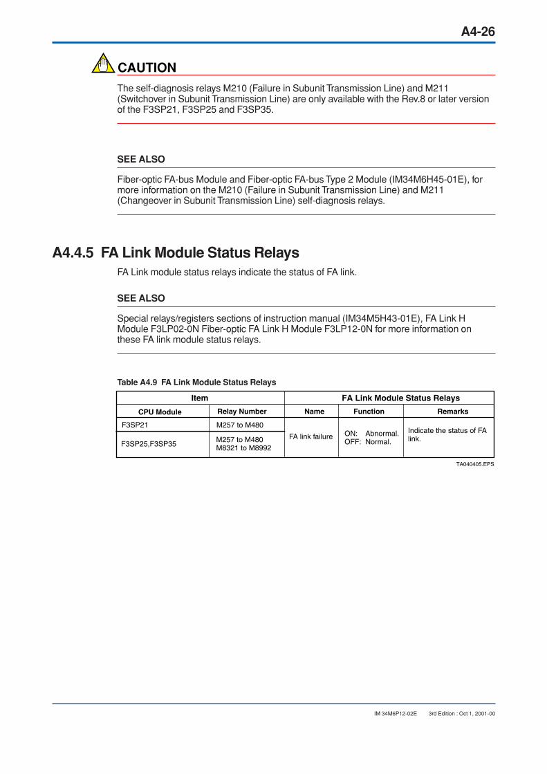
A4-26
IM 34M6P12-02E 3rd Edition : Oct 1, 2001-00
CAUTION
The self-diagnosis relays M210 (Failure in Subunit Transmission Line) and M211(Switchover in Subunit Transmission Line) are only available with the Rev.8 or later versionof the F3SP21, F3SP25 and F3SP35.
SEE ALSO
Fiber-optic FA-bus Module and Fiber-optic FA-bus Type 2 Module (IM34M6H45-01E), formore information on the M210 (Failure in Subunit Transmission Line) and M211(Changeover in Subunit Transmission Line) self-diagnosis relays.
A4.4.5 FA Link Module Status RelaysFA Link module status relays indicate the status of FA link.
SEE ALSO
Special relays/registers sections of instruction manual (IM34M5H43-01E), FA Link HModule F3LP02-0N Fiber-optic FA Link H Module F3LP12-0N for more information onthese FA link module status relays.
Table A4.9 FA Link Module Status Relays
Item FA Link Module Status Relays
TA040405.EPS
CPU Module
F3SP25,F3SP35
Relay Number Name Function Remarks
M257 to M480
FA link failure ON: Abnormal.OFF: Normal.
Indicate the status of FA link.M257 to M480
M8321 to M8992
F3SP21

A4-27
IM 34M6P12-02E 3rd Edition : Oct 1, 2001-00
A4.5 Timers (T)There are four types of timer: 1-ms, 10-ms and 100-ms timers and a 100-ms continuoustimer. For each type, you can assign the number of timers using the configuration function.However, you are not allowed to assign more than 16 points of 1-ms timers.
A4.5.1 1-ms, 10-ms, and 100-ms Timers1-ms, 10-ms, and 100-ms timers are synchronized-scan, decremental timers which updatetheir current values and turn on/off their time-out relays using an END process.
Setpoints: 1-ms timer 0.001 to 32.767 s
10-ms timer 0.01 to 327.67 s
100-ms timer 0.1 to 3276.7 s
Each timer starts counting at the rising edge of the timer input, and expires when thecurrent value reaches 0. When the timer expires, its time-out relay turns on. The time-outrelay is used for a contact a or b. The timer is reset at the falling edge of the timer input andthe current value returns to the timer’s setpoint.
X00501 I0001 Y00601
X00301 T001
I0002
Y00603
X005021sT001TIM
Timer input
Timer inputX00502
Current valueT001
Time-out relayT001
ON
OFF
Setpoint
0
ON
OFF
1 s
F040501.EPS
Figure A4.17 Timer

A4-28
IM 34M6P12-02E 3rd Edition : Oct 1, 2001-00
A4.5.2 100-ms Continuous TimerA 100-ms continuous timer is a synchronized-scan, decremental timer which updates itscurrent value and turns on/off its time-out relay using an END process.
Setpoint: 0.1 to 3276.7 s
The 100-ms continuous timer retains its current value and the state of its time-out relayeven when the timer input is set to OFF. When the timer input is set to ON again, the timerstarts counting from the value it retains. When the timer input is set to OFF after the con-tinuous timer expires, the timer is reset, the current value returns to the setpoint, and thetime-out relay is set to OFF.
If you want to reset the continuous timer before it expires, write “0” to the time using a MOVinstruction (MOV 0 Tnnn) when the timer input is in an OFF state.
X00501 I0001 Y00601
X00301 T241
I0002
Y00603
X0050210sT241TIM
Timer input
Timer inputX00502
Current valueT241
Time-out relayT241
ON
OFF
Setpoint
0
ON
OFF
(1) + (2) =10 sF040502.EPS
(1) (2)
Figure A4.18 100-ms Continuous Timers
With the configuration function, you can configure a range of timers to determine whetheror not they retain their current values when the power is turned off. By default, all timers areset so as not to retain their current values. If you set the timers to this option, their currentvalues are reset to their setpoints when you:
• turn off the power and turn it on again;
• change the operation mode to Run or Debug with the programming tool; or
• send a device clearance command from the programming tool.
If you set the timers so as to retain their current values, the latest results are retained afterpower-off. In this case, the timers are reset to their setpoints when you send a deviceclearance command from the programming tool.
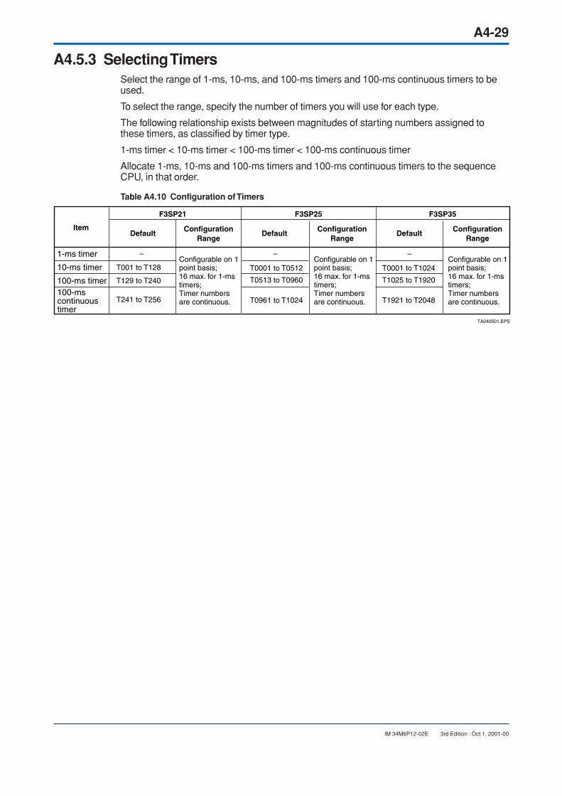
A4-29
IM 34M6P12-02E 3rd Edition : Oct 1, 2001-00
A4.5.3 Selecting TimersSelect the range of 1-ms, 10-ms, and 100-ms timers and 100-ms continuous timers to beused.
To select the range, specify the number of timers you will use for each type.
The following relationship exists between magnitudes of starting numbers assigned tothese timers, as classified by timer type.
1-ms timer < 10-ms timer < 100-ms timer < 100-ms continuous timer
Allocate 1-ms, 10-ms and 100-ms timers and 100-ms continuous timers to the sequenceCPU, in that order.
Table A4.10 Configuration of Timers
ItemDefault Configuration
RangeDefault Configuration
RangeDefault Configuration
Range
F3SP21 F3SP25 F3SP35
TA040501.EPS
T0001 to T0512
T0513 to T0960
T0961 to T1024
T0001 to T1024
T1025 to T1920
T1921 to T2048
T001 to T128
T129 to T240
T241 to T256
– – –
100-mscontinuoustimer
1-ms timer
10-ms timer
100-ms timer
Configurable on 1 point basis;16 max. for 1-ms timers;Timer numbers are continuous.
Configurable on 1 point basis;16 max. for 1-ms timers;Timer numbers are continuous.
Configurable on 1 point basis;16 max. for 1-ms timers;Timer numbers are continuous.

A4-30
IM 34M6P12-02E 3rd Edition : Oct 1, 2001-00
A4.6 Counters (C)The counters are decremental counters and have two types of input: count input and resetinput.
A counter detects the rising edge of a count input and updates the current value when acounter instruction is executed. The counter terminates when its current value reaches 0.
When the counter terminates, its end-of-count relay turns on. The count-up relay is usedfor a contact a or b.
The counter is reset at the rising edge of the reset input and the current value returns to thecounter’s setpoint. Count input is not accepted when the reset input is on.
Setpoint: 1 to 32767
X00501
C001 X00504 Y00602
X00502100C001CNT
Reset inputX00502
Count inputX00502
Current valueC001
Count-up relayC001
ON
OFF
ON
OFF
100
0
ON
OFF
Reset input
Count input
99 98
1
F040601.EPS
Figure A4.19 Counter
With the configuration function, you can configure a range of counters to determinewhether or not they retain their current values when the power is turned off. By default, allcounters are set so as to retain their current values. If you set the counters otherwise, theircurrent values are reset to their setpoints when you:
• turn off the power and turn it on again;
• change the operation mode to Run or Debug with the programming tool; or
• send a device clearance command from the programming tool.
If you set the counters so as to retain their current values, the latest results are retainedafter power-off. In this case, the counters are reset to their setpoints when you send adevice clearance command from the programming tool.

A4-31
IM 34M6P12-02E 3rd Edition : Oct 1, 2001-00
A4.6.1 Selecting CountersSelect the range of counters to be used.
Table A4.11 Configuration of Counters
ItemDefault Configuration
RangeDefault Configuration
RangeDefault Configuration
Range
F3SP21 F3SP25 F3SP35
TA040601.EPS
T0001 to T1024
C0001 to C1024
T0001 to T2048
C0001 to T1024
T001 to T256
C001 to C256
Sum of timers and counters: 512 points max., on 1 point basisTimer numbers: T001 to T512Counter numbers: C001 to C512
Sum of timers and counters: 2048 points max., on 1 point basisTimer numbers: T0001 to T2048Counter numbers: C0001 to C2048
Sum of timers and counters: 3072 points max., on 1 point basisTimer numbers: T0001 to T3072Counter numbers: C0001 to C3072
Devicesize
Timer (T)
Counter (C)
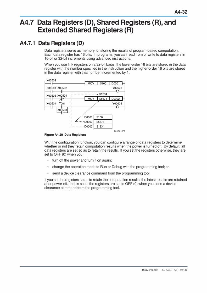
A4-32
IM 34M6P12-02E 3rd Edition : Oct 1, 2001-00
A4.7 Data Registers (D), Shared Registers (R), andExtended Shared Registers (R)
A4.7.1 Data Registers (D)Data registers serve as memory for storing the results of program-based computation.Each data register has 16 bits. In programs, you can read from or write to data registers in16-bit or 32-bit increments using advanced instructions.
When you use link registers on a 32-bit basis, the lower-order 16 bits are stored in the dataregister with the number specified in the instruction and the higher-order 16 bits are storedin the data register with that number incremented by 1.
X00503
X00501 T001
X00504
X00502
X00503
Y00602
Y00601
MOV $5678
$1234
D0002
X00501
X00502MOV $100 D0001
$100
$5678
$1234
D0001
D0002
D0003
F040701.EPS
Figure A4.20 Data Registers
With the configuration function, you can configure a range of data registers to determinewhether or not they retain computation results when the power is turned off. By default, alldata registers are set so as to retain the results. If you set the registers otherwise, they areset to OFF (0) when you:
• turn off the power and turn it on again;
• change the operation mode to Run or Debug with the programming tool; or
• send a device clearance command from the programming tool.
If you set the registers so as to retain the computation results, the latest results are retainedafter power-off. In this case, the registers are set to OFF (0) when you send a deviceclearance command from the programming tool.
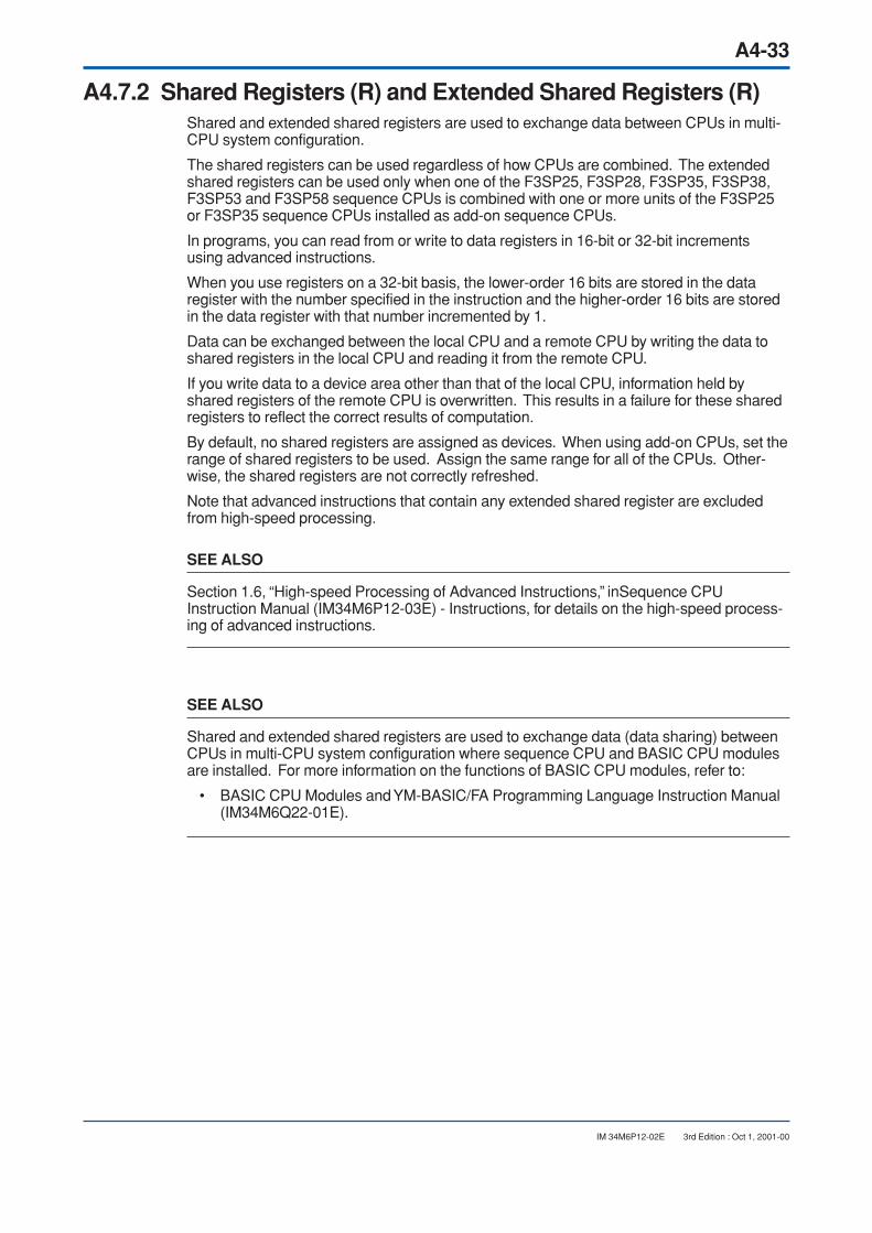
A4-33
IM 34M6P12-02E 3rd Edition : Oct 1, 2001-00
A4.7.2 Shared Registers (R) and Extended Shared Registers (R)Shared and extended shared registers are used to exchange data between CPUs in multi-CPU system configuration.
The shared registers can be used regardless of how CPUs are combined. The extendedshared registers can be used only when one of the F3SP25, F3SP28, F3SP35, F3SP38,F3SP53 and F3SP58 sequence CPUs is combined with one or more units of the F3SP25or F3SP35 sequence CPUs installed as add-on sequence CPUs.
In programs, you can read from or write to data registers in 16-bit or 32-bit incrementsusing advanced instructions.
When you use registers on a 32-bit basis, the lower-order 16 bits are stored in the dataregister with the number specified in the instruction and the higher-order 16 bits are storedin the data register with that number incremented by 1.
Data can be exchanged between the local CPU and a remote CPU by writing the data toshared registers in the local CPU and reading it from the remote CPU.
If you write data to a device area other than that of the local CPU, information held byshared registers of the remote CPU is overwritten. This results in a failure for these sharedregisters to reflect the correct results of computation.
By default, no shared registers are assigned as devices. When using add-on CPUs, set therange of shared registers to be used. Assign the same range for all of the CPUs. Other-wise, the shared registers are not correctly refreshed.
Note that advanced instructions that contain any extended shared register are excludedfrom high-speed processing.
SEE ALSO
Section 1.6, “High-speed Processing of Advanced Instructions,” inSequence CPUInstruction Manual (IM34M6P12-03E) - Instructions, for details on the high-speed process-ing of advanced instructions.
SEE ALSO
Shared and extended shared registers are used to exchange data (data sharing) betweenCPUs in multi-CPU system configuration where sequence CPU and BASIC CPU modulesare installed. For more information on the functions of BASIC CPU modules, refer to:
• BASIC CPU Modules and YM-BASIC/FA Programming Language Instruction Manual(IM34M6Q22-01E).
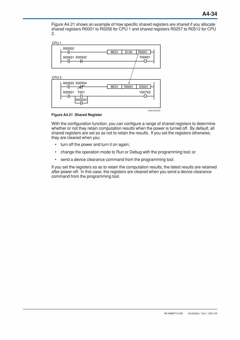
A4-34
IM 34M6P12-02E 3rd Edition : Oct 1, 2001-00
Figure A4.21 shows an example of how specific shared registers are shared if you allocateshared registers R0001 to R0256 for CPU 1 and shared registers R0257 to R0512 for CPU2.
X00502 Y00601X00501
X00502MOV
CPU 1
CPU 2
$100 R0001
X00503
X00501 T001
X00504
X00503
Y00702
MOV R0001 D0001
F040702.EPS
Figure A4.21 Shared Register
With the configuration function, you can configure a range of shared registers to determinewhether or not they retain computation results when the power is turned off. By default, allshared registers are set so as not to retain the results. If you set the registers otherwise,they are cleared when you:
• turn off the power and turn it on again;
• change the operation mode to Run or Debug with the programming tool; or
• send a device clearance command from the programming tool.
If you set the registers so as to retain the computation results, the latest results are retainedafter power-off. In this case, the registers are cleared when you send a device clearancecommand from the programming tool.
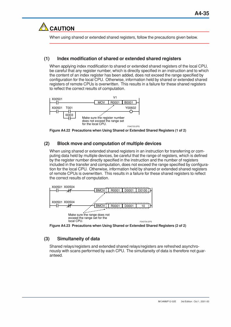
A4-35
IM 34M6P12-02E 3rd Edition : Oct 1, 2001-00
CAUTION
When using shared or extended shared registers, follow the precautions given below.
(1) Index modification of shared or extended shared registers
When applying index modification to shared or extended shared registers of the local CPU,be careful that any register number, which is directly specified in an instruction and to whichthe content of an index register has been added, does not exceed the range specified byconfiguration for the local CPU. Otherwise, information held by shared or extended sharedregisters of remote CPUs is overwritten. This results in a failure for these shared registersto reflect the correct results of computation.
X00501
X00501 T001
I0003
Y00602
MOV R0001
V1
B0001
Make sure the register numberdoes not exceed the range setfor the local CPU.
F040703.EPS
Figure A4.22 Precautions when Using Shared or Extended Shared Registers (1 of 2)
(2) Block move and computation of multiple devices
When using shared or extended shared registers in an instruction for transferring or com-puting data held by multiple devices, be careful that the range of registers, which is definedby the register number directly specified in the instruction and the number of registersincluded in the transfer and computation, does not exceed the range specified by configura-tion for the local CPU. Otherwise, information held by shared or extended shared registersof remote CPUs is overwritten. This results in a failure for these shared registers to reflectthe correct results of computation.
X00504X00501
X00501BMOV R0001 D0001 D0100
BMOV R0001 D0001 10
X00504
Make sure the range does notexceed the range set for thelocal CPU. F040704.EPS
Figure A4.23 Precautions when Using Shared or Extended Shared Registers (2 of 2)
(3) Simultaneity of data
Shared relays/registers and extended shared relays/registers are refreshed asynchro-nously with scans performed by each CPU. The simultaneity of data is therefore not guar-anteed.
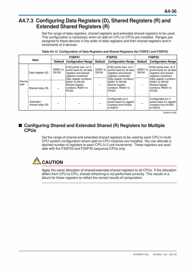
A4-36
IM 34M6P12-02E 3rd Edition : Oct 1, 2001-00
A4.7.3 Configuring Data Registers (D), Shared Registers (R) andExtended Shared Registers (R)
Set the range of data registers, shared registers and extended shared registers to be used.This configuration is necessary when an add-on CPU or CPUs are installed. Ranges areassigned to these devices in the order of data registers and then shared registers and inincrements of 2 devices.
Table A4.12 Configuration of Data Registers and Shared Registers (for F3SP21 and F3SP25)
ItemF3SP25 F3SP35
Default DefaultConfiguration Range Configuration RangeF3SP21
Default
D0001 to D8192
D0001 to D5120
–
– – – –
– –
D0001 to D8192
Configuration Range
8192 points max. on 2 points basis for all data registers and shared registers combinedData register numbers: D0001 to D8192Shared register numbers: R0001 to R1024
8192 points max. on 2 points basis for all data registers and shared registers combinedData register numbers: D0001 to D8192Shared register numbers: R0001 to R1024
5120 points max. on 2 points basis for all data registers and shared registers combinedData register numbers: D0001 to D5120Shared register numbers: R0001 to R1024
Configurable on 2 points basis for register numbers from R1025 to R3072
Configurable ion 2 points basis for register numbers from R1025 to R3072
Data register (D)
Shared relay (R)
Extendedshared relay (R)
TA040701.EPS
Devicesize
Configuring Shared and Extended Shared (R) Registers for MultipleCPUs
Set the range of shared and extended shared registers to be used by each CPU in multi-CPU system configuration where add-on CPU modules are installed. You can allocate adesired number of registers to each CPU in 2 unit increments. These registers are avail-able with the F3SP25 and F3SP35 sequence CPUs only.
CAUTION
Apply the same allocation of shared/extended shared registers to all CPUs. If the allocationdiffers from CPU to CPU, shared refreshing is not performed correctly. This results in afailure for these registers to reflect the correct results of computation.
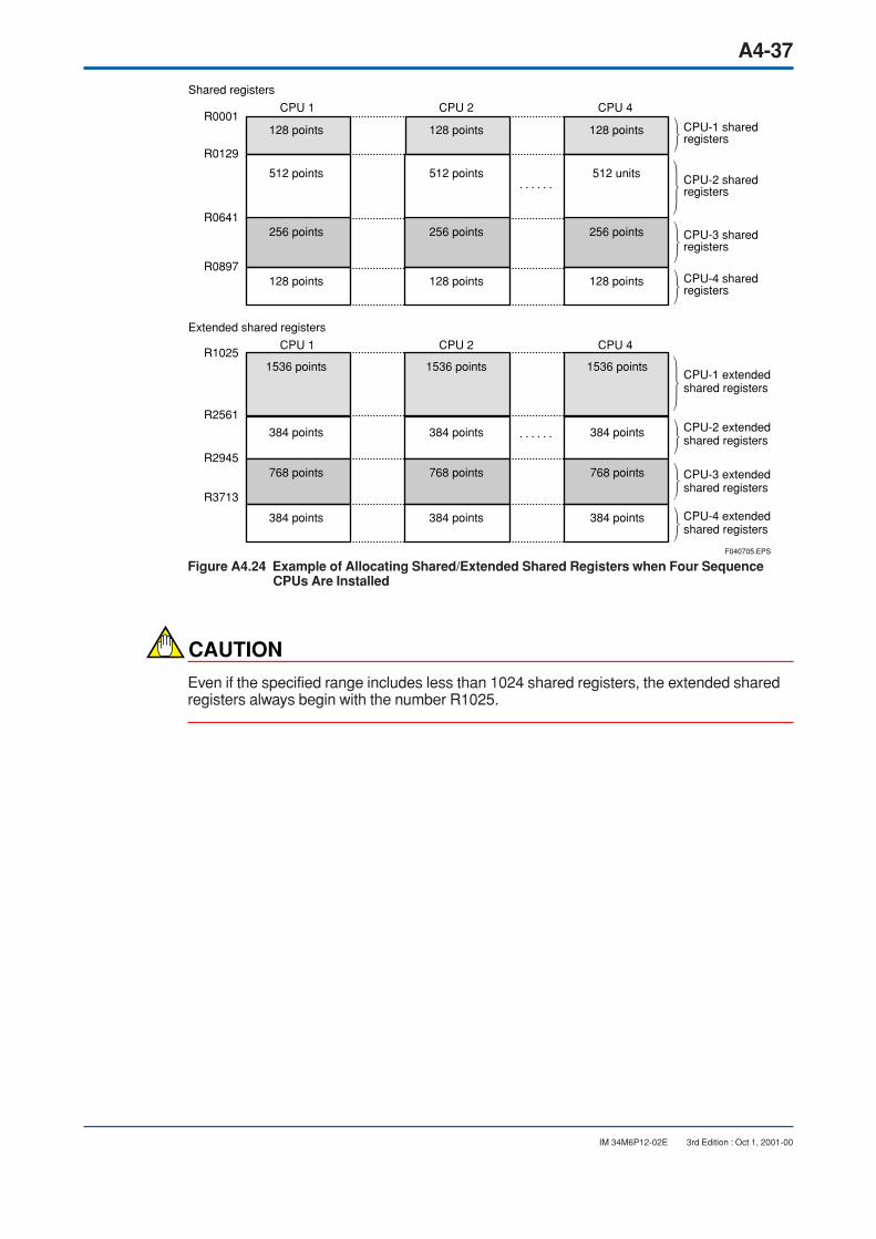
A4-37
IM 34M6P12-02E 3rd Edition : Oct 1, 2001-00
Shared registers
R0001
R0129
R0641
R0897
Extended shared registers
128 points
512 points
256 points
128 points
CPU-1 sharedregisters
CPU-2 sharedregisters
CPU-3 sharedregisters
CPU-4 sharedregisters
CPU 1 CPU 2 CPU 4
R1025
R2561
R2945
R3713
1536 points
384 points
768 points
384 points
CPU-1 extendedshared registers
CPU-2 extendedshared registers
CPU-3 extendedshared registers
CPU-4 extendedshared registers
CPU 1
768 points
384 points
CPU 2
768 points
384 points
CPU 4
128 points
512 points
256 points
128 points
128 points
512 units
256 points
128 points
1536 points
384 points
1536 points
384 points
F040705.EPS
Figure A4.24 Example of Allocating Shared/Extended Shared Registers when Four Sequence CPUs Are Installed
CAUTION
Even if the specified range includes less than 1024 shared registers, the extended sharedregisters always begin with the number R1025.

A4-38
IM 34M6P12-02E 3rd Edition : Oct 1, 2001-00
A4.7.4 Setting Initial DataUsing the configuration function, set the initial values of data registers (D) to be used at thestart of program execution.
The data items to be configured are the data registers’ starting number and their quantityand initial data values. After this configuration, the preset initial data values are stored inthe specified data registers when the program starts. This configuration is useful when alarge volume of initial data needs to be set by a program or when the initial data needs tobe saved. You can set initial data in a maximum of 1024 data registers.
Starting number =1
D0001
D1024
D4096
Quantity = 1024
The initial data is transferredat the start of programexecution.
F040706.EPS
Figure A4.25 Setting Initial Data
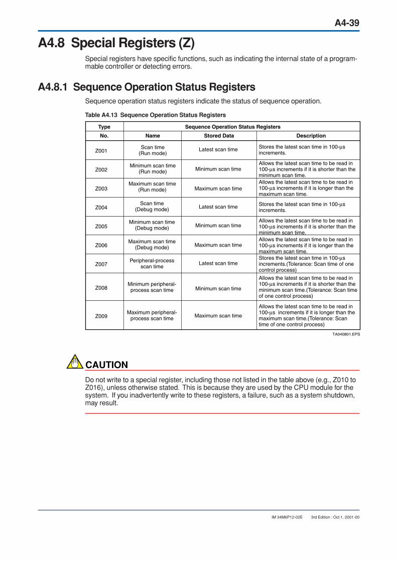
A4-39
IM 34M6P12-02E 3rd Edition : Oct 1, 2001-00
A4.8 Special Registers (Z)Special registers have specific functions, such as indicating the internal state of a program-mable controller or detecting errors.
A4.8.1 Sequence Operation Status RegistersSequence operation status registers indicate the status of sequence operation.
Table A4.13 Sequence Operation Status Registers
Scan time(Run mode)
Minimum scan time(Run mode)
No.
Type Sequence Operation Status Registers
Name Stored Data Description
Maximum scan time(Run mode)
Z001
Z002
Z003
Z004
Z005
Z006
Z007
Z008
Z009
Scan time(Debug mode)
Minimum scan time(Debug mode)
Maximum scan time(Debug mode)
Peripheral-processscan time
Minimum peripheral-process scan time
Maximum peripheral-process scan time
Stores the latest scan time in 100-µs increments.
Allows the latest scan time to be read in 100-µs increments if it is shorter than the minimum scan time.Allows the latest scan time to be read in 100-µs increments if it is longer than the maximum scan time.
Stores the latest scan time in 100-µs increments.
Allows the latest scan time to be read in 100-µs increments if it is shorter than the minimum scan time.Allows the latest scan time to be read in 100-µs increments if it is longer than the maximum scan time.
TA040801.EPS
Stores the latest scan time in 100-µs increments.(Tolerance: Scan time of one control process)
Allows the latest scan time to be read in 100-µs increments if it is shorter than the minimum scan time.(Tolerance: Scan time of one control process)
Allows the latest scan time to be read in 100-µs increments if it is longer than the maximum scan time.(Tolerance: Scan time of one control process)
Latest scan time
Minimum scan time
Maximum scan time
Minimum scan time
Maximum scan time
Minimum scan time
Maximum scan time
Latest scan time
Latest scan time
CAUTION
Do not write to a special register, including those not listed in the table above (e.g., Z010 toZ016), unless otherwise stated. This is because they are used by the CPU module for thesystem. If you inadvertently write to these registers, a failure, such as a system shutdown,may result.
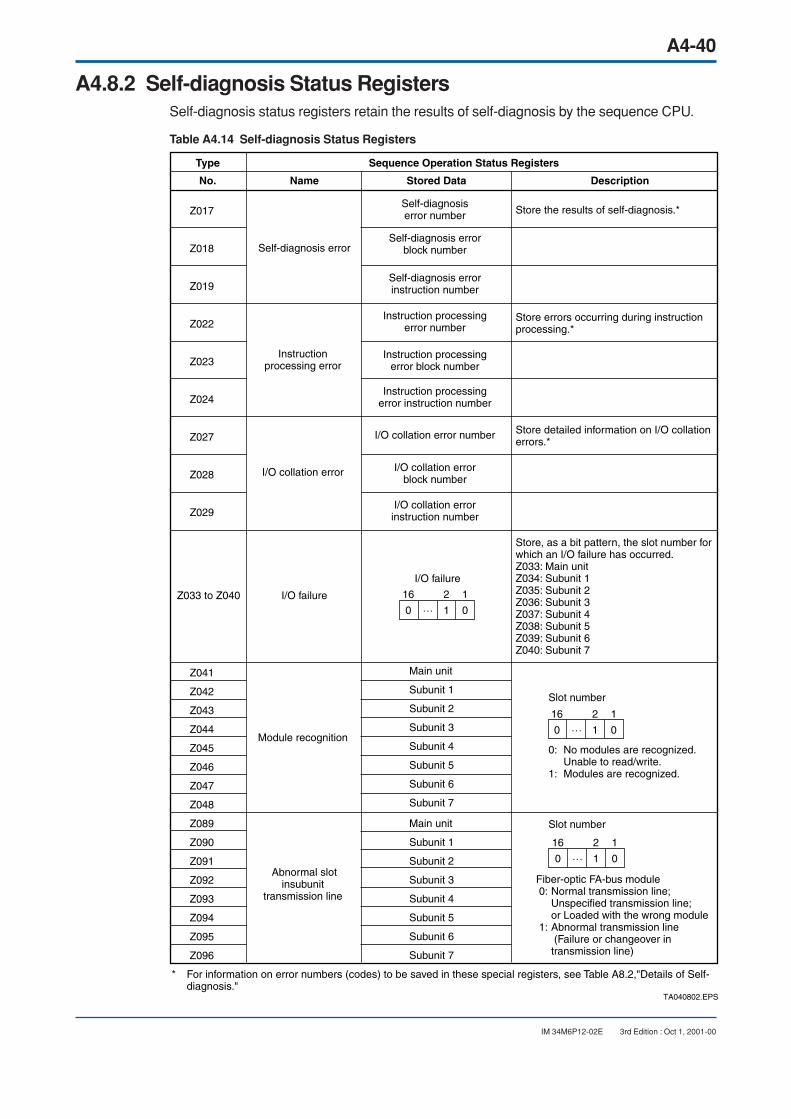
A4-40
IM 34M6P12-02E 3rd Edition : Oct 1, 2001-00
A4.8.2 Self-diagnosis Status RegistersSelf-diagnosis status registers retain the results of self-diagnosis by the sequence CPU.
Table A4.14 Self-diagnosis Status Registers
Self-diagnosis error
No.
Type Sequence Operation Status Registers
Name Stored Data Description
Z017
Z018
Z019
Z022
Z023
Z024
Z027
Z028
Z029
Z041
Z042
Z043
Z044
Z045
Z046
Z047
Z048
Z089
Z090
Z091
Z092
Z093
Z094
Z095
Z096
Instructionprocessing error
I/O collation error
I/O failure
Module recognition
Abnormal slotinsubunit
transmission line
Store the results of self-diagnosis.*
Store errors occurring during instruction processing.*
TA040802.EPS
Store detailed information on I/O collation errors.*
Store, as a bit pattern, the slot number for which an I/O failure has occurred.Z033: Main unitZ034: Subunit 1Z035: Subunit 2Z036: Subunit 3Z037: Subunit 4Z038: Subunit 5Z039: Subunit 6Z040: Subunit 7
* For information on error numbers (codes) to be saved in these special registers, see Table A8.2,"Details of Self-diagnosis."
Self-diagnosiserror number
Self-diagnosis errorblock number
Self-diagnosis errorinstruction number
I/O collation errorblock number
I/O collation errorinstruction number
I/O failure
Instruction processingerror block number
Instruction processingerror instruction number
Instruction processingerror number
I/O collation error number
Z033 to Z040
16 2 1
0 1 0…
16 2 1
0 1 0…
16 2 1
0 1 0…
Main unit
Subunit 1
Subunit 2
Subunit 3
Subunit 4
Subunit 5
Subunit 6
Subunit 7
Main unit
Subunit 1
Subunit 2
Subunit 3
Subunit 4
Subunit 5
Subunit 6
Subunit 7
Slot number
Slot number
0: No modules are recognized. Unable to read/write.1: Modules are recognized.
Fiber-optic FA-bus module 0: Normal transmission line; Unspecified transmission line;
or Loaded with the wrong module 1: Abnormal transmission line
(Failure or changeover in transmission line)

A4-41
IM 34M6P12-02E 3rd Edition : Oct 1, 2001-00
CAUTION
• The special registers Z041 to Z048 (Module Recognition) are only available with theRev.8 or later version of the F3SP21, F3SP25 and F3SP35.
• The special registers Z089 to Z096 (Abnormal Slot in Subunit Transmission Line) areonly available with the Rev.8 or later version of the F3SP21, F3SP25 and F3SP35.
SEE ALSO
Fiber-optic FA-bus Module and Fiber-optic FA-bus Type 2 Module (IM34M6H45-01E), formore information on the Z089 to Z096 special registers (Abnormal Slot in SubunitTransmission Line).
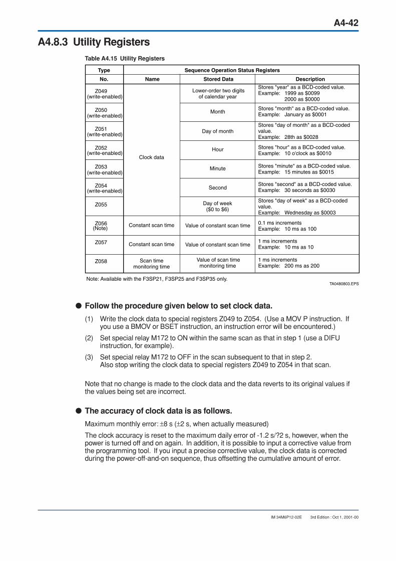
A4-42
IM 34M6P12-02E 3rd Edition : Oct 1, 2001-00
A4.8.3 Utility RegistersTable A4.15 Utility Registers
Clock data
No.
Type Sequence Operation Status Registers
Name Stored Data Description
Z049
Z050
Z051
Z052
Z053
Z054
Z055
Z056
Z057
Z058
Stores "month" as a BCD-coded value.Example: January as $0001
Stores "day of month" as a BCD-coded value.Example: 28th as $0028
Stores "hour" as a BCD-coded value.Example: 10 o'clock as $0010
Stores "minute" as a BCD-coded value.Example: 15 minutes as $0015
0.1 ms incrementsExample: 10 ms as 100
1 ms incrementsExample: 10 ms as 10
1 ms incrementsExample: 200 ms as 200
Stores "second" as a BCD-coded value.Example: 30 seconds as $0030
Stores "day of week" as a BCD-coded value.Example: Wednesday as $0003
Stores "year" as a BCD-coded value.Example: 1999 as $0099
2000 as $0000
Lower-order two digitsof calendar year
Month
Day of month
Value of constant scan time
Value of constant scan time
Value of scan timemonitoring time
Minute
Second
Day of week($0 to $6)
Hour
(write-enabled)
(write-enabled)
(write-enabled)
(write-enabled)
(write-enabled)
(write-enabled)
(Note) Constant scan time
Constant scan time
Scan timemonitoring time
Note: Available with the F3SP21, F3SP25 and F3SP35 only.TA0480803.EPS
Follow the procedure given below to set clock data.
(1) Write the clock data to special registers Z049 to Z054. (Use a MOV P instruction. Ifyou use a BMOV or BSET instruction, an instruction error will be encountered.)
(2) Set special relay M172 to ON within the same scan as that in step 1 (use a DIFUinstruction, for example).
(3) Set special relay M172 to OFF in the scan subsequent to that in step 2.Also stop writing the clock data to special registers Z049 to Z054 in that scan.
Note that no change is made to the clock data and the data reverts to its original values ifthe values being set are incorrect.
The accuracy of clock data is as follows.
Maximum monthly error: ±8 s (±2 s, when actually measured)
The clock accuracy is reset to the maximum daily error of -1.2 s/?2 s, however, when thepower is turned off and on again. In addition, it is possible to input a corrective value fromthe programming tool. If you input a precise corrective value, the clock data is correctedduring the power-off-and-on sequence, thus offsetting the cumulative amount of error.

A4-43
IM 34M6P12-02E 3rd Edition : Oct 1, 2001-00
A4.8.4 FA Link Module Status RegistersFA Link module status registers indicate the status of FA link.
SEE ALSO
Special relays/registers sections in FA Link Module F3LP02-0N Fiber-optic FA Link ModuleF3LP12-0N (IM34M5H43-01E) for more information on the FA link module status registers.
Table A4.16 FA Link Module Status Registers
Local station status
Cyclictransmissiontime
Local station status
Cyclictransmissiontime
Local station status
Cyclictransmissiontime
Local station status
Cyclictransmissiontime
Local station status
Cyclictransmissiontime
Local station status
Cyclictransmissiontime
Local station status
Cyclictransmissiontime
Local station status
Cyclictransmissiontime
No.
Type Sequence Operation Status Registers
Name Stored Data Description
Z065
Z066
Z070
Z071
Z257 (Note)
Z258 (Note)
Z262 (Note)
Z263 (Note)
Z267 (Note)
Z268 (Note)
Z272 (Note)
Z273 (Note)
Z277 (Note)
Z278 (Note)
Z282 (Note)
Z283 (Note)
TA040804.EPS
0: Under initialization1: Offline2: Online
0: Under initialization1: Offline2: Online
0: Under initialization1: Offline2: Online
0: Under initialization1: Offline2: Online
0: Under initialization1: Offline2: Online
0: Under initialization1: Offline2: Online
0: Under initialization1: Offline2: Online
0: Under initialization1: Offline2: Online
FA link 2
FA link 1
FA link 1 1 ms increments
FA link 2 1 ms increments
FA link 3
FA link 3 1 ms increments
FA link 4
FA link 4 1 ms increments
FA link 5
FA link 5 1 ms increments
FA link 6
FA link 6 1 ms increments
FA link 7
FA link 7 1 ms increments
FA link 8
FA link 8 1 ms increments
Note: Available with the F3SP25 and F3SP35 only.

A4-44
IM 34M6P12-02E 3rd Edition : Oct 1, 2001-00
A4.8.5 CPU Module Status RegistersCPU module status registers indicate the status of a CPU.
Table A4.17 CPU Module Status Registers
Number of storeduser logs
Z105
No.
Type Sequence Operation Status Registers
Name Stored Data Description
TA040805.EPS
See Section A6.14, "User Log Management Function," for information on user logs.

A4-45
IM 34M6P12-02E 3rd Edition : Oct 1, 2001-00
A4.9 Index Registers (V)Index registers are used to apply index modification to devices.
You can use these registers for both basic instructions and advanced instructions to makeindex modifications.
Use these registers when specifying a device number by adding the content of an indexregister to a device whose number is directly specified in an instruction.
SEE ALSO
Section 1.7, “Index Modification,” in the instruction manual (IM34M6P12-03E), SequenceCPU - Instructions, for more information on the index registers.
X00503
X00501 T001
X00504
X00502
X00503
Y00602
Y00601
MOV D0001
V01 V02
D0100
I0001
X00502MOV 100 V01
V01
I(0001+100)=I0101 D(0001+100)=D0101F040901.EPS
Figure A4.26 Index Registers
CAUTION
Examination of whether or not the device number specified using an index register exceedsthe given configuration range, is not performed on the system side of the sequence CPUmodule. The configuration range may be exceeded depending on the content of the indexregister used, resulting in the selection of the wrong device. Be careful when specifying thedevice number.
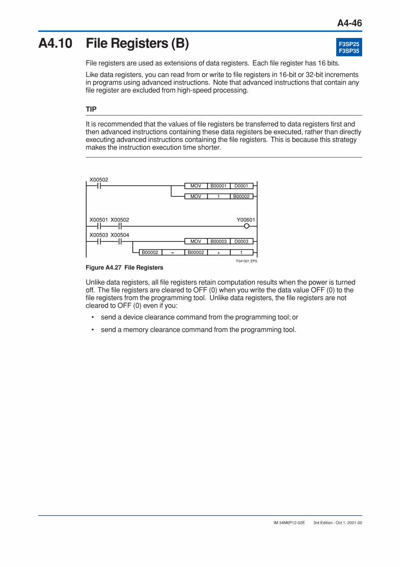
A4-46
IM 34M6P12-02E 3rd Edition : Oct 1, 2001-00
A4.10 File Registers (B)File registers are used as extensions of data registers. Each file register has 16 bits.
Like data registers, you can read from or write to file registers in 16-bit or 32-bit incrementsin programs using advanced instructions. Note that advanced instructions that contain anyfile register are excluded from high-speed processing.
TIP
It is recommended that the values of file registers be transferred to data registers first andthen advanced instructions containing these data registers be executed, rather than directlyexecuting advanced instructions containing the file registers. This is because this strategymakes the instruction execution time shorter.
X00501 X00502 Y00601
X00503 X00504
X00502D0001B00001MOV
B000021MOV
D0003B00003MOV
1+B00002=B00002
F041001.EPS
Figure A4.27 File Registers
Unlike data registers, all file registers retain computation results when the power is turnedoff. The file registers are cleared to OFF (0) when you write the data value OFF (0) to thefile registers from the programming tool. Unlike data registers, the file registers are notcleared to OFF (0) even if you:
• send a device clearance command from the programming tool; or
• send a memory clearance command from the programming tool.
F3SP25F3SP35
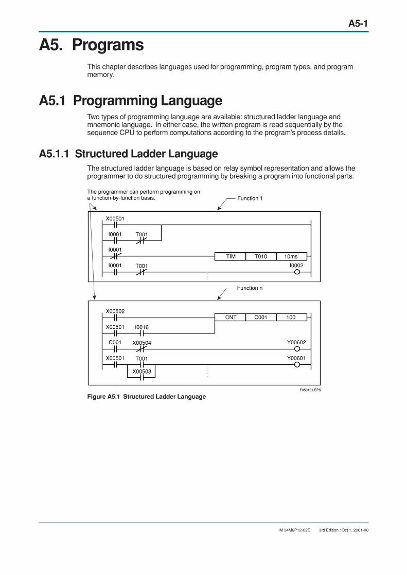
A5-1
IM 34M6P12-02E 3rd Edition : Oct 1, 2001-00
A5. ProgramsThis chapter describes languages used for programming, program types, and programmemory.
A5.1 Programming LanguageTwo types of programming language are available: structured ladder language andmnemonic language. In either case, the written program is read sequentially by thesequence CPU to perform computations according to the program’s process details.
A5.1.1 Structured Ladder LanguageThe structured ladder language is based on relay symbol representation and allows theprogrammer to do structured programming by breaking a program into functional parts.
X00501
C001 X00504 Y00602
X00502100C001CNT
I0016
X00501 T001
X00503
Y00601
I0001
I0001
T001
X00501
10msT010TIM
I0001 T001 I0002
The programmer can perform programming on a function-by-function basis. Function 1
Function n
F050101.EPS
Figure A5.1 Structured Ladder Language

A5-2
IM 34M6P12-02E 3rd Edition : Oct 1, 2001-00
A5.1.2 Mnemonic LanguageThe mnemonic language is designed to describe a program by breaking its process detailsinto instruction, source and destination sections. Like the structured ladder language, themnemonic language allows the programmer to perform programming on a function-by-function basis.
LD
OUT
LD
AND
MOV
I0001
Y00602
X00501
X00502
D0001 , D0002
Instruction section
Instruction section Source section Destination sectionF050102.EPS
Figure A5.2 Mnemonic Language

A5-3
IM 34M6P12-02E 3rd Edition : Oct 1, 2001-00
A5.2 Program Types and ConfigurationTwo types of programs are available: blocks and executable programs.
A5.2.1 Blocks and Executable Programs
BlocksA block refers to a set of circuits entered through the programming tool.
Parts of each program written on a function-by-function basis using the structured ladderlanguage or mnemonic language are managed as blocks. Since the program can bemaintained or reused block by block, program development becomes extremely easy. Asingle block can contain steps up to 10 K.
CAUTION
It is not possible for the CPU to execute a separate block.
X00503 X00504 Y00602
X00501 X00502
X00503
Y00601
I0001
X00501 X00502 I0003
Y00602
Block 1
Block n
Circuit
F050201.EPS
Figure A5.3 Blocks
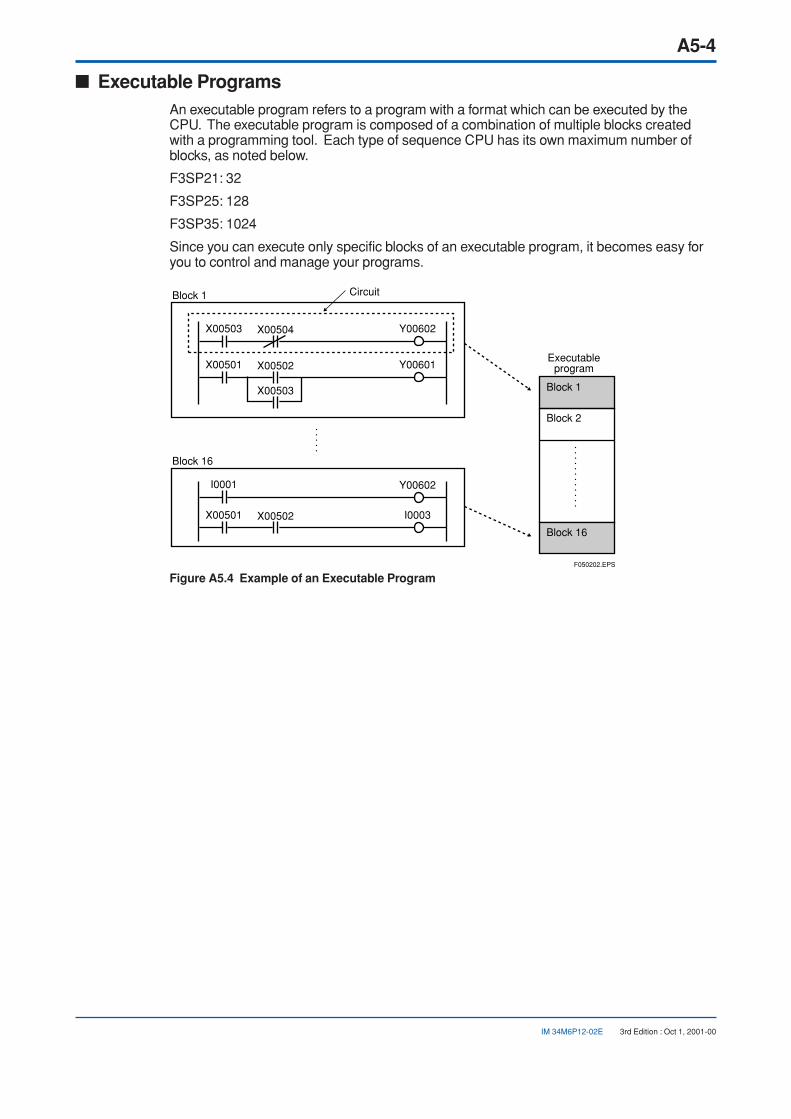
A5-4
IM 34M6P12-02E 3rd Edition : Oct 1, 2001-00
Executable ProgramsAn executable program refers to a program with a format which can be executed by theCPU. The executable program is composed of a combination of multiple blocks createdwith a programming tool. Each type of sequence CPU has its own maximum number ofblocks, as noted below.
F3SP21: 32
F3SP25: 128
F3SP35: 1024
Since you can execute only specific blocks of an executable program, it becomes easy foryou to control and manage your programs.
X00503 X00504 Y00602
X00501 X00502
X00503
Y00601
I0001
X00501 X00502 I0003
Y00602
Block 1
Block 16
Circuit
Block 1
Block 2
Block 16
Executableprogram
F050202.EPS
Figure A5.4 Example of an Executable Program

A5-5
IM 34M6P12-02E 3rd Edition : Oct 1, 2001-00
A5.2.2 Programs Composing an Executable ProgramPrograms that compose an executable program are classified into main routine programs,subroutine programs and interrupt programs, according to their functions.
Main routine program
Main routine program
Main routine program
Subroutine program
Subroutine program
Subroutine program
Interrupt program
Block 1
Block 2
Block n
Executableprogram
F050203.EPS
Figure A5.5 Programs Composing an Executable Program

A5-6
IM 34M6P12-02E 3rd Edition : Oct 1, 2001-00
Main Routine ProgramsA main routine program is always executed in each scan. Since the main routine programis written in the structured ladder language, it is composed of multiple blocks.
You can execute a main routine program by either executing all blocks of the program orexecuting only specific blocks.
SUB
RET
Block 1
Block n-1
Block n
Programexecution
This subroutineprogram isexcluded fromthe execution.
F050204.EPS
Figure A5.6 The Way a Main Routine Program Is Executed

A5-7
IM 34M6P12-02E 3rd Edition : Oct 1, 2001-00
Subroutine ProgramsA subroutine program is executed when a CALL instruction is given by a main routineprogram. Use this program when you want to run a specific process two or more timeswithin one scan. A subroutine program can be placed in any location in a block.
In a case where the operation mode in which only specific blocks are executed is selected,a subroutine program is executed even if it is located in a yet-to-be-executed block andcalled from a block being executed.
Subroutine programs can be nested to a maximum depth of eight layers (nesting means tocall a subroutine from within another subroutine).
CALL
RET
Block 1
Block n-1
Block n
Programexecution
SUB
Subroutine program
F050205.EPS
Programexecution
Figure A5.7 The Way a Subroutine Program Is Executed
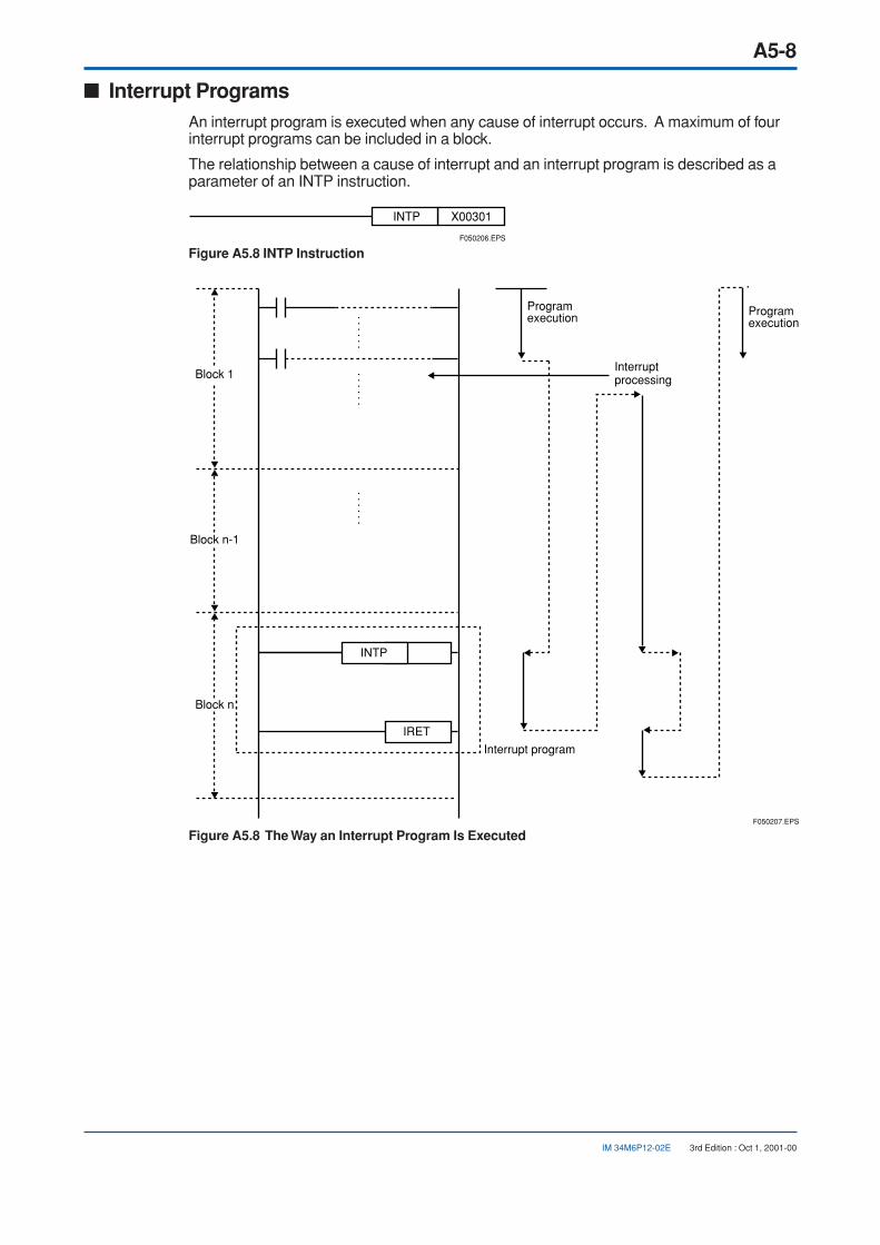
A5-8
IM 34M6P12-02E 3rd Edition : Oct 1, 2001-00
Interrupt ProgramsAn interrupt program is executed when any cause of interrupt occurs. A maximum of fourinterrupt programs can be included in a block.
The relationship between a cause of interrupt and an interrupt program is described as aparameter of an INTP instruction.
X00301INTP
F050206.EPS
Figure A5.8 INTP Instruction
IRET
Block 1
Block n-1
Block n
Programexecution
INTP
Interrupt program
Interruptprocessing
Programexecution
F050207.EPS
Figure A5.8 The Way an Interrupt Program Is Executed
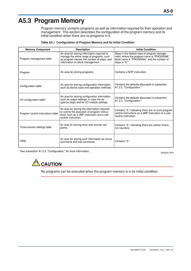
A5-9
IM 34M6P12-02E 3rd Edition : Oct 1, 2001-00
A5.3 Program MemoryProgram memory contains programs as well as information required for their operation andmanagement. This section describes the configuration of the program memory and itsinitial condition when there are no programs in it.
Table A5.1 Configuration of Program Memory and Its Initial Condition
TA050301.EPS
Memory Component Description Initial Condition
Program management table
Program
Configuration table*
I/O configuration table*
Program control instructions table
Timer/counter settings table
Utility
An area for storing information required to manage the entire range of programs, such as program names, the number of steps, and information on block management.
An area for storing the information required to control the execution of program instruc-tions, such as a JMP instruction and a sub-routine instruction.
An area for storing timer and counter set-points.
An area for storing such information as circuit comments and sub-comments.
An area for storing configuration information, such as device sizes and operation methods.
An area for storing configuration information such as output settings, in case the se-quence stops and for I/O module settings.
An area for storing programs.
Stays in the default state of program manage-ment, where the program name is "PROGRAM," block name is "PROGRAM," and the number of steps is "0."
Contains "0," indicating there are no such program control instructions as a JMP instruction or a sub-routine instruction.
Contains the defaults discussed in subsection A1.2.3, "Configuration."
Contains the defaults discussed in subsection A1.2.3, "Configuration."
Contains "0."
Contains "0," indicating there are neither timers nor counters.
Contains a NOP instruction.
* See subsection A1.2.3, "Configuration," for more information.
CAUTION
No programs can be executed when the program memory is in its initial condition.
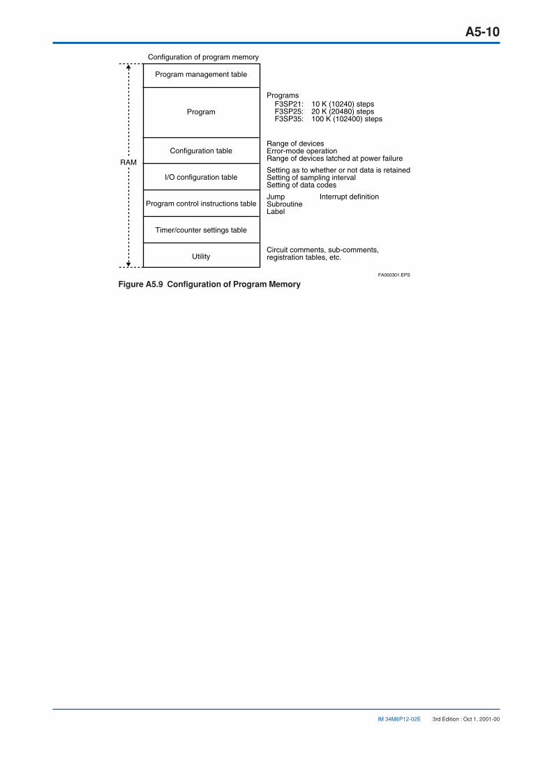
A5-10
IM 34M6P12-02E 3rd Edition : Oct 1, 2001-00
Configuration of program memory
Program management table
Program
Configuration table
I/O configuration table
Program control instructions table
Timer/counter settings table
Utility
ProgramsF3SP21: 10 K (10240) stepsF3SP25: 20 K (20480) stepsF3SP35: 100 K (102400) steps
Range of devicesError-mode operationRange of devices latched at power failure
Setting as to whether or not data is retainedSetting of sampling intervalSetting of data codes
Jump Interrupt definitionSubroutineLabel
Circuit comments, sub-comments, registration tables, etc.
RAM
FA050301.EPS
Figure A5.9 Configuration of Program Memory
A6-1
IM 34M6P12-02E 3rd Edition : Oct 1, 2001-00
A6. FunctionsThis chapter describes functions which can be executed by the CPU module, suchas the execution of specified blocks and debugging operation.
A6.1 Function ListThe following tables summarize the functions provided by the sequence CPU.
Table A6.1 Functions Provided by the Sequence CPU
Sequence CPU Function Page
TA060101.EPS
Function Overview
Constant scan Executes a sequence program at certain time intervals.
Execution of all blocks/specified blocks
Debugging function Supports debugging operations, such as forced set/reset.
Program protection function
Operation setup function Specifies the operation mode of the CPU and its actions.
Online edit function
Sampling trace function (*1)
Personal computer link function (*2)
Macro instruction function (*1)
A6-5
A6-6
A6-13
A6-17
A6-3
A6-19
A6-27
A6-31
A6-48
Specifies how an executable program is processed.Specified blocks are executed using ACT and INACT instructions.
Protects programs by means of password.This function has two modes: executable program protection and block protection.
Makes on-line modifications or changes to a program in the program memory of the CPU.
Acquires and displays states of multiple devices for up to 1024 scans.
Performs the same level of communication as that of a personal computer link module, when a personal computer or a monitor is connected to the programming tool port.
Allows the user to create and register new, customized instructions.
*1 Available with the F3SP25 and F3SP35 only.*2 Available with the F3SP21, F3SP25 and F3SP35 only.
Table A6.2 ROM Management (Writer) Function
ROM Management (Writer) Function Page
TA060102.EPS
Function Overview
Writes a program or data to the ROM.
File-to-ROM transfer function
CPU-to-ROM transfer (ROM copy) function
File/ROM cross-check function
ROM clearing function
Writes programs or data to the ROM.
A6-25
A6-25
A6-25
A6-25
Cross-checks the ROM data with the details of programs in the programming tool*.
Erases the ROM data.
* Refers to either the FA-M3 Programming Tool WideField or Ladder Diagram Support Program M3.
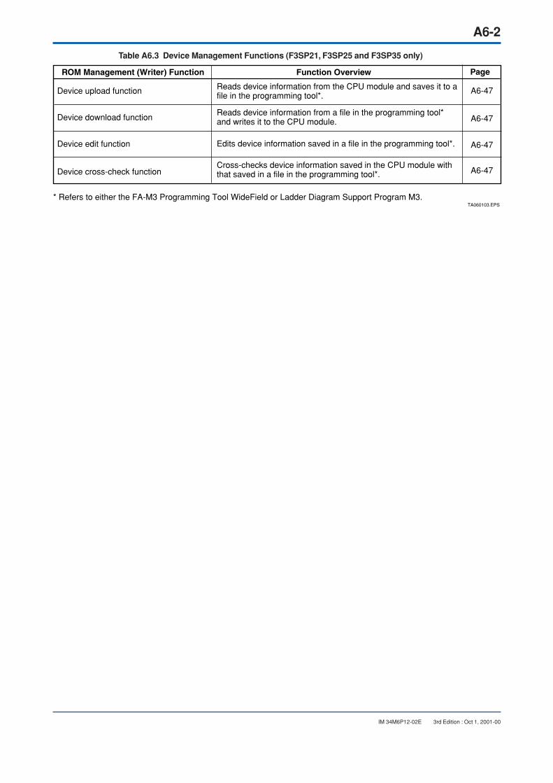
A6-2
IM 34M6P12-02E 3rd Edition : Oct 1, 2001-00
Table A6.3 Device Management Functions (F3SP21, F3SP25 and F3SP35 only)
ROM Management (Writer) Function Page
TA060103.EPS
Function Overview
Device upload function
Device download function
Device edit function
Device cross-check function
A6-47
A6-47
A6-47
A6-47
Reads device information from the CPU module and saves it to a file in the programming tool*.
Reads device information from a file in the programming tool* and writes it to the CPU module.
Cross-checks device information saved in the CPU module with that saved in a file in the programming tool*.
Edits device information saved in a file in the programming tool*.
* Refers to either the FA-M3 Programming Tool WideField or Ladder Diagram Support Program M3.
A6-3
IM 34M6P12-02E 3rd Edition : Oct 1, 2001-00
A6.2 Operation Setup FunctionThe operation setup function sets up the CPU operation mode and initializes programs anddevices. This function can be used by entering a command from the programming tool,personal computer link module, or an add-on CPU.
Run ModeThe CPU begins running a program from its first instruction, similar to when the power isturned on. When the power is turned on or the mode is changed from “stop” to “run,” theCPU sets all devices to 0, except for latching-type devices, before executing the program.When the CPU enters the Run mode, functions available only in the Debug or Stop modeare disabled.
Debug ModeThe CPU begins running a program from its first instruction, similar to when the power isturned on. When the power is turned on or the mode is changed from “Stop” to “Debug,” theCPU sets all devices to 0, except for latching-type devices, before executing the program.Be sure to disable the Debug mode and enter the Run mode when you have completedyour debugging and tuning tasks.
Stop ModeThe CPU stops running the program. External output data is retained (ON) or not retained(OFF), depending on the settings of the configuration item “external output to be retained incase of sequence stop.” This mode does not work when the CPU has already stoppedrunning the program.
Clearing Memory Stop
This function deletes a program or programs and sets all devices to 0. Stop running theprogram before using this function.
Clearing Devices Stop
This function sets all latching-type devices, excluding file registers for the F3SP25 andF3SP35, to 0. Stop running the program before using this function. To clear file registers,use the device edit function of the device management function to set all the file registerdata to 0 and write the data to the CPU module using the device write function.
See Also
For details on the device management function, see Section A6.12, “Device ManagementFunction.”

A6-4
IM 34M6P12-02E 3rd Edition : Oct 1, 2001-00
CAUTION
The following are precautions you should follow when using the functions described in thischapter:
• Some functions are not available in all the operation modes.
Note that the following marks are used when explaining each function, in order toindicate that the function in question is available in the cited mode or modes.
Run , Debug and Stop
Unless otherwise specified, the function can be used in any operation mode.
• The scan time may become longer for some functions.
When you finish using such a function, be sure to disable it before running the system.
Be especially careful when using any function that works in Debug mode. When yourdebugging and tuning tasks are complete, always disable the function and enter Runmode.
• Be sure to use the ROM writer functions when you operate the ROM pack.
Note that the following mark is used when explaining each ROM writer function toindicate that the function is available in ROM Writer mode.
ROM writer
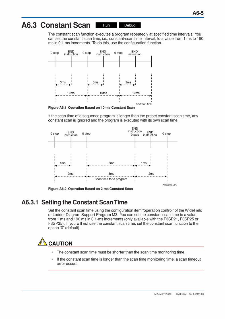
A6-5
IM 34M6P12-02E 3rd Edition : Oct 1, 2001-00
A6.3 Constant Scan Run Debug
The constant scan function executes a program repeatedly at specified time intervals. Youcan set the constant scan time, i.e., constant-scan time interval, to a value from 1 ms to 190ms in 0.1 ms increments. To do this, use the configuration function.
0 step ENDinstruction 0 step END
instruction 0 step ENDinstruction
3ms
10ms 10ms 10ms
5ms 2ms
FA060201.EPS
Figure A6.1 Operation Based on 10-ms Constant Scan
If the scan time of a sequence program is longer than the preset constant scan time, anyconstant scan is ignored and the program is executed with its own scan time.
0 step ENDinstruction 0 step 0 step
ENDinstruction
0 stepEND
instruction
1ms
2ms 3ms
3ms
2ms
1ms
Scan time for a program
FA060202.EPS
Figure A6.2 Operation Based on 2-ms Constant Scan
A6.3.1 Setting the Constant Scan TimeSet the constant scan time using the configuration item “operation control” of the WideFieldor Ladder Diagram Support Program M3. You can set the constant scan time to a valuefrom 1 ms and 190 ms in 0.1-ms increments (only available with the F3SP21, F3SP25 orF3SP35). If you will not use the constant scan time, set the constant scan function to theoption “0” (default).
CAUTION
• The constant scan time must be shorter than the scan time monitoring time.
• If the constant scan time is longer than the scan time monitoring time, a scan timeouterror occurs.
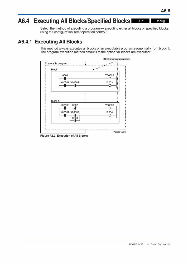
A6-6
IM 34M6P12-02E 3rd Edition : Oct 1, 2001-00
A6.4 Executing All Blocks/Specified Blocks Run Debug
Select the method of executing a program — executing either all blocks or specified blocks,using the configuration item “operation control.”
A6.4.1 Executing All BlocksThis method always executes all blocks of an executable program sequentially from block 1.The program execution method defaults to the option “all blocks are executed.”
I0001 Y00602
X00501 X00502 I0003
X00503 I0002 Y00603
X00501 X00502
I0003
I0004
Executable program
Block 1
Block n
All blocks are executed.
FA060301.EPS
Figure A6.3 Execution of All Blocks
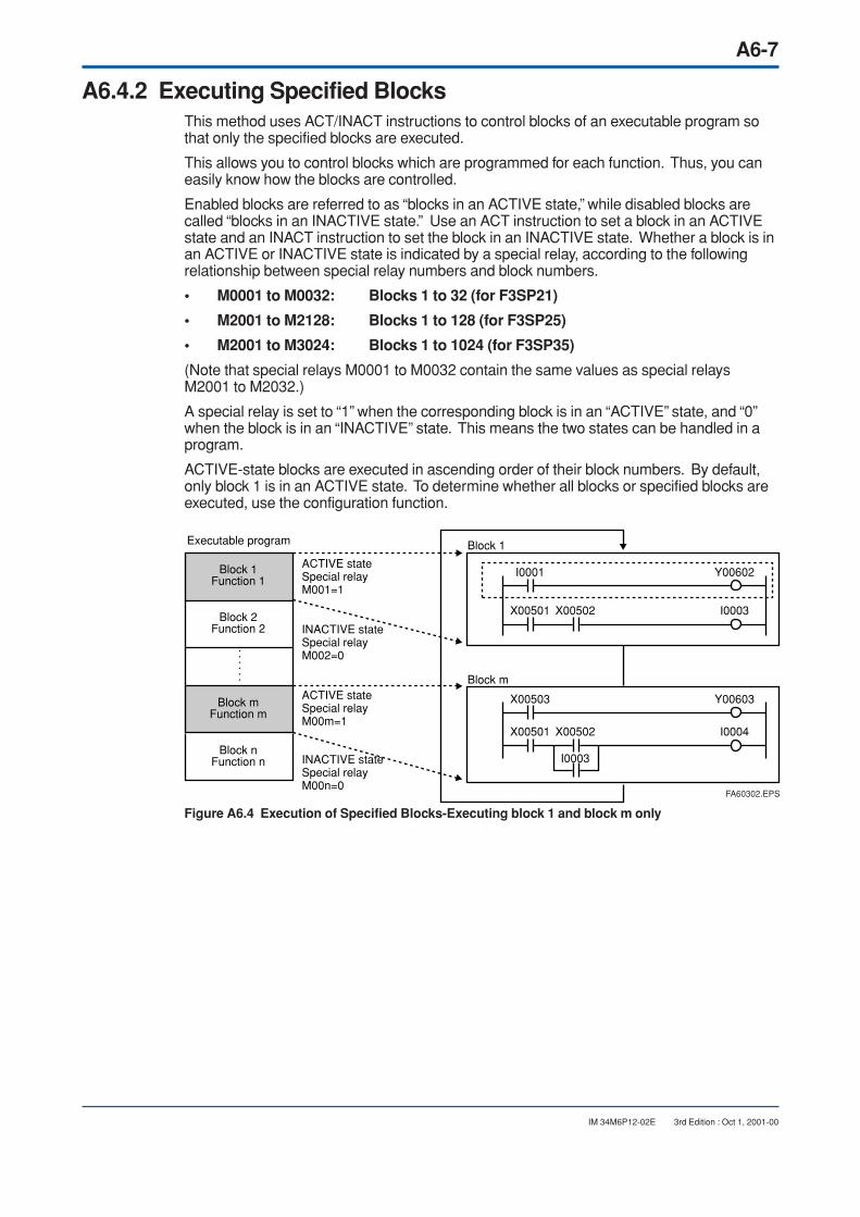
A6-7
IM 34M6P12-02E 3rd Edition : Oct 1, 2001-00
A6.4.2 Executing Specified BlocksThis method uses ACT/INACT instructions to control blocks of an executable program sothat only the specified blocks are executed.
This allows you to control blocks which are programmed for each function. Thus, you caneasily know how the blocks are controlled.
Enabled blocks are referred to as “blocks in an ACTIVE state,” while disabled blocks arecalled “blocks in an INACTIVE state.” Use an ACT instruction to set a block in an ACTIVEstate and an INACT instruction to set the block in an INACTIVE state. Whether a block is inan ACTIVE or INACTIVE state is indicated by a special relay, according to the followingrelationship between special relay numbers and block numbers.
• M0001 to M0032: Blocks 1 to 32 (for F3SP21)
• M2001 to M2128: Blocks 1 to 128 (for F3SP25)
• M2001 to M3024: Blocks 1 to 1024 (for F3SP35)
(Note that special relays M0001 to M0032 contain the same values as special relaysM2001 to M2032.)
A special relay is set to “1” when the corresponding block is in an “ACTIVE” state, and “0”when the block is in an “INACTIVE” state. This means the two states can be handled in aprogram.
ACTIVE-state blocks are executed in ascending order of their block numbers. By default,only block 1 is in an ACTIVE state. To determine whether all blocks or specified blocks areexecuted, use the configuration function.
I0001 Y00602
X00501 X00502 I0003
X00503 Y00603
X00501 X00502
I0003
I0004
Block 1
Block m
Executable program
Block 1Function 1
Block 2Function 2
Block mFunction m
Block nFunction n
ACTIVE stateSpecial relayM001=1
INACTIVE stateSpecial relayM002=0
ACTIVE stateSpecial relayM00m=1
INACTIVE stateSpecial relayM00n=0
FA60302.EPS
Figure A6.4 Execution of Specified Blocks-Executing block 1 and block m only

A6-8
IM 34M6P12-02E 3rd Edition : Oct 1, 2001-00
A6.4.3 Operation when Specified Blocks Are EnabledBlocks that have been enabled with an ACT instruction are initialized at the end of thescan in which they were enabled. It is from the next scan that the blocks enabled with anACT instruction actually start.
Executable program
Block 1Function 1
Block 1Function 1
Block 1Function 1
Block 2Function 2
Block 2Function 2
Block 1Function 1
Block 2Function 2
Block mFunction m
Block mFunction m
Block nFunction n
nth scan
ACT Block 2
ACT Block m
ACT
Executable program
Block 1Function 1
Block 2Function 2
Block mFunction m
Block nFunction n
ACT
(n + 1)-th scan
(n + 2)-th scan
Special relayM2001=1
Special relayM2001=1
Special relayM2002=1
Special relayM2001=1
Special relayM2002=1
Special relayM200m=1
Next scan
Next scan
Next scan
FA060303.EPS
Figure A6.5 Operation when Specified Blocks Are Enabled
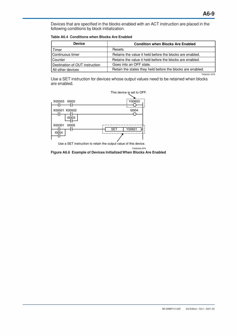
A6-9
IM 34M6P12-02E 3rd Edition : Oct 1, 2001-00
Devices that are specified in the blocks enabled with an ACT instruction are placed in thefollowing conditions by block initialization.
Table A6.4 Conditions when Blocks Are Enabled
Device
TA060301.EPS
Condition when Blocks Are Enabled
Timer Resets.Continuous timer Retains the value it held before the blocks are enabled.Counter Retains the value it held before the blocks are enabled.Destination of OUT instruction Goes into an OFF state.All other devices Retain the states they held before the blocks are enabled.
Use a SET instruction for devices whose output values need to be retained when blocksare enabled.
X00503 I0002 Y00603
X00501 X00502
I0003
I0004
X00301 I0005
I0004Y00601SET
This device is set to OFF.
Use a SET instruction to retain the output value of this device.FA060304.EPS
Figure A6.6 Example of Devices Initialized When Blocks Are Enabled
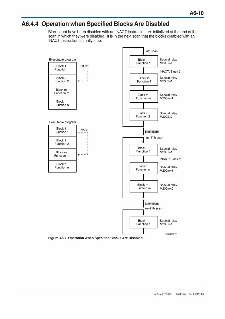
A6-10
IM 34M6P12-02E 3rd Edition : Oct 1, 2001-00
A6.4.4 Operation when Specified Blocks Are DisabledBlocks that have been disabled with an INACT instruction are initialized at the end of thescan in which they were disabled. It is in the next scan that the blocks disabled with anINACT instruction actually stop.
Executable program
Block 1 Function 1
Block 1 Function 1
Block m Function m
Block 2 Function 2
Block 2 Function 2
Block 1 Function 1
Block n Function n
Block m Function m
Block m Function m
Block n Function n
nth scan
INACT: Block 2
INACT
Executable program
Block 1 Function 1
Block 2 Function 2
Block m Function m
Block n Function n
INACT
(n+1)th scan
Special relayM2001=1
Special relayM200m=1
Special relayM2002=0
Special relayM2001=1
Special relayM200m=1
Special relayM200m=0
Next scan
F060403.EPS
Block 1 Function 1
INACT: Block m
Special relayM2001=1
Next scan
(n+2)th scan
Block 2 Function 2
Special relayM2002=1
Figure A6.7 Operation When Specified Blocks Are Disabled
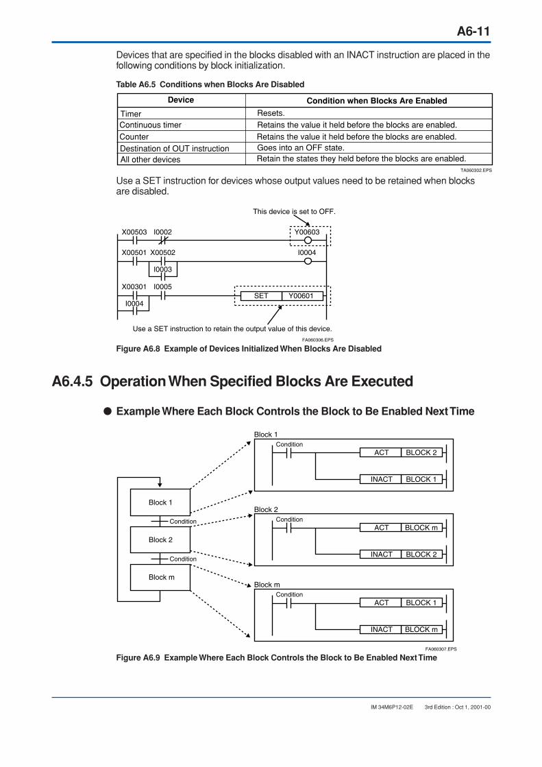
A6-11
IM 34M6P12-02E 3rd Edition : Oct 1, 2001-00
Devices that are specified in the blocks disabled with an INACT instruction are placed in thefollowing conditions by block initialization.
Table A6.5 Conditions when Blocks Are Disabled
Device
TA060302.EPS
Condition when Blocks Are Enabled
Timer Resets.Continuous timer Retains the value it held before the blocks are enabled.Counter Retains the value it held before the blocks are enabled.Destination of OUT instruction Goes into an OFF state.All other devices Retain the states they held before the blocks are enabled.
Use a SET instruction for devices whose output values need to be retained when blocksare disabled.
X00503 I0002 Y00603
X00501 X00502
I0003
I0004
X00301 I0005
I0004Y00601SET
This device is set to OFF.
Use a SET instruction to retain the output value of this device.FA060306.EPS
Figure A6.8 Example of Devices Initialized When Blocks Are Disabled
A6.4.5 Operation When Specified Blocks Are Executed
Example Where Each Block Controls the Block to Be Enabled Next Time
BLOCK 2ACT
BLOCK 1INACT
Block 1Condition
Condition
Condition
BLOCK mACT
BLOCK 2INACT
Block 2Condition
BLOCK 1ACT
BLOCK mINACT
Block mCondition
Block 1
Block 2
Block m
FA060307.EPS
Figure A6.9 Example Where Each Block Controls the Block to Be Enabled Next Time
A6-12
IM 34M6P12-02E 3rd Edition : Oct 1, 2001-00
Example Where Blocks to Be Enabled Are Controlled by Creating Sched-uler
BLOCK 2ACT
BLOCK nINACT
Block 1Condition
BLOCK 3ACT
BLOCK 2INACT
Condition
BLOCK 1ACT
BLOCK m
BLOCK 3INACT
Condition
BLOCK nACT
BLOCK 1INACT
BLOCK mINACT
Condition
Block 1
Block 2
Block 3
Block 1 Block m
Block n
ACT
Condition
Condition
Condition
Condition Condition
F060408.EPS
Condition
Figure A6.10 Example Where Blocks to Be Enabled Are Controlled by Creating Scheduler
Create a scheduler for block 1 which is initially in an ACTIVE state.

A6-13
IM 34M6P12-02E 3rd Edition : Oct 1, 2001-00
A6.5 Debugging Functions
A6.5.1 Step Operation Debug
Step operation executes only one instruction at a time as dictated by a specified instructionnumber. After completing the instruction, the CPU goes into a Pause state and stopsprogram execution. Use the programming tool to specify the instruction number.
I0001 Y00602
X00501 I0003
X00503 Y00603I0002
X00502
One instruction is executed. FA060401.EPS
Figure A6.11 Step Operation
CAUTION
The clock data of both timers and special relays are updated only when the CPU is execut-ing a program during step operation. That is, the CPU does not update the data when in aPause state.
Step operation is ignored if such a control instruction as JMP or CALL is executed. TheCPU resumes normal instruction execution from the instruction to which control has beenpassed.
X00501
I0001 Y00602
X00503 Y00603
X00501 X00502
I0002
I0004
LBL 1
LBL 1
JMP
I0003
An instruction whichis to be suspendednext
The instruction executioncontrol moves here.
An instruction isexecuted normally.
FA060402.EPS
Figure A6.12 Step Operation when a JMP (or CALL) Instruction Is Executed
If the CPU is paused due to a control instruction, you can re-input the jump destination ofthe control instruction as the start-of-step-operation instruction number, in order to continuestep operation.
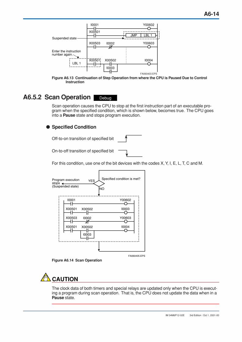
A6-14
IM 34M6P12-02E 3rd Edition : Oct 1, 2001-00
X00501
I0001 Y00602
X00503 Y00603
X00501 X00502
I0002
I0004
LBL 1
LBL 1
JMP
I0003
Suspended state
Enter the instructionnumber again.
FA060403.EPS
Figure A6.13 Continuation of Step Operation from where the CPU is Paused Due to ControlInstruction
A6.5.2 Scan Operation Debug
Scan operation causes the CPU to stop at the first instruction part of an executable pro-gram when the specified condition, which is shown below, becomes true. The CPU goesinto a Pause state and stops program execution.
Specified Condition
Off-to-on transition of specified bit
On-to-off transition of specified bit
For this condition, use one of the bit devices with the codes X, Y, I, E, L, T, C and M.
I0001 Y00602
NO
YES
I0003
X00501 I0003X00502
X00503 Y00603I0002
X00501 I0004X00502
Program executionstops(Suspended state)
Specified condition is met?
FA060405.EPS
Figure A6.14 Scan Operation
CAUTION
The clock data of both timers and special relays are updated only when the CPU is execut-ing a program during scan operation. That is, the CPU does not update the data when in aPause state.

A6-15
IM 34M6P12-02E 3rd Edition : Oct 1, 2001-00
CAUTION
Scan operation is only possible with Ladder Diagram Support Program M3, and is notpossible with WideField.
A6.5.3 Partial Operation Debug
Partial operation executes only a specific range of instructions defined by the starting andending instruction numbers. Use a programming tool to specify the starting and endingnumbers. This mode of operation is used when only part of program performance needs tobe verified.
I0001 Y00602
I0003
X00501 I0003X00502
X00503 Y00603I0002
X00501 I0004X00502
Only this part of aprogram is executed.
Start instruction number
End instruction number
FA060406.EPS
Figure A6.15 Partial Operation
CAUTION
Partial operation is only possible with Ladder Diagram Support Program M3, and is notpossible with WideField.
A6.5.4 Forced SET/RESET Debug Stop
A forced SET/RESET instruction forcibly sets a specified bit device to ON/OFF, regardlessof program execution. You can use the instruction for a maximum of 32 bit devices of alltypes combined. Only bit devices are supported, i.e., X, Y, I, E, L, T and C devices.
If a forced SET instruction is applied to a timer (T) or a counter (C), the timer expires or thecounter terminates.
A forced SET/RESET instruction remains valid until you:
• disable the instruction,
• change the operation mode to RUN, or
• turn off the power.
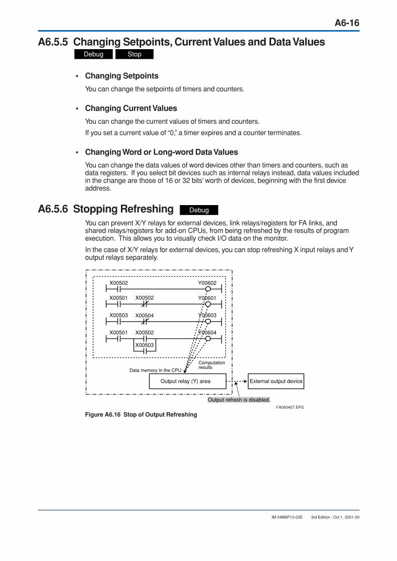
A6-16
IM 34M6P12-02E 3rd Edition : Oct 1, 2001-00
A6.5.5 Changing Setpoints, Current Values and Data Values Debug Stop
• Changing Setpoints
You can change the setpoints of timers and counters.
• Changing Current Values
You can change the current values of timers and counters.
If you set a current value of “0,” a timer expires and a counter terminates.
• Changing Word or Long-word Data Values
You can change the data values of word devices other than timers and counters, such asdata registers. If you select bit devices such as internal relays instead, data values includedin the change are those of 16 or 32 bits’ worth of devices, beginning with the first deviceaddress.
A6.5.6 Stopping RefreshingYou can prevent X/Y relays for external devices, link relays/registers for FA links, andshared relays/registers for add-on CPUs, from being refreshed by the results of programexecution. This allows you to visually check I/O data on the monitor.
In the case of X/Y relays for external devices, you can stop refreshing X input relays and Youtput relays separately.
X00501
X00502 Y00602
Y00601
X00503 Y00603
X00501 X00502
X00504
Y00604
X00503
X00502
Computationresults
Data memory in the CPU
Output relay (Y) area External output device
Output refresh is disabled.FA060407.EPS
Figure A6.16 Stop of Output Refreshing
Debug
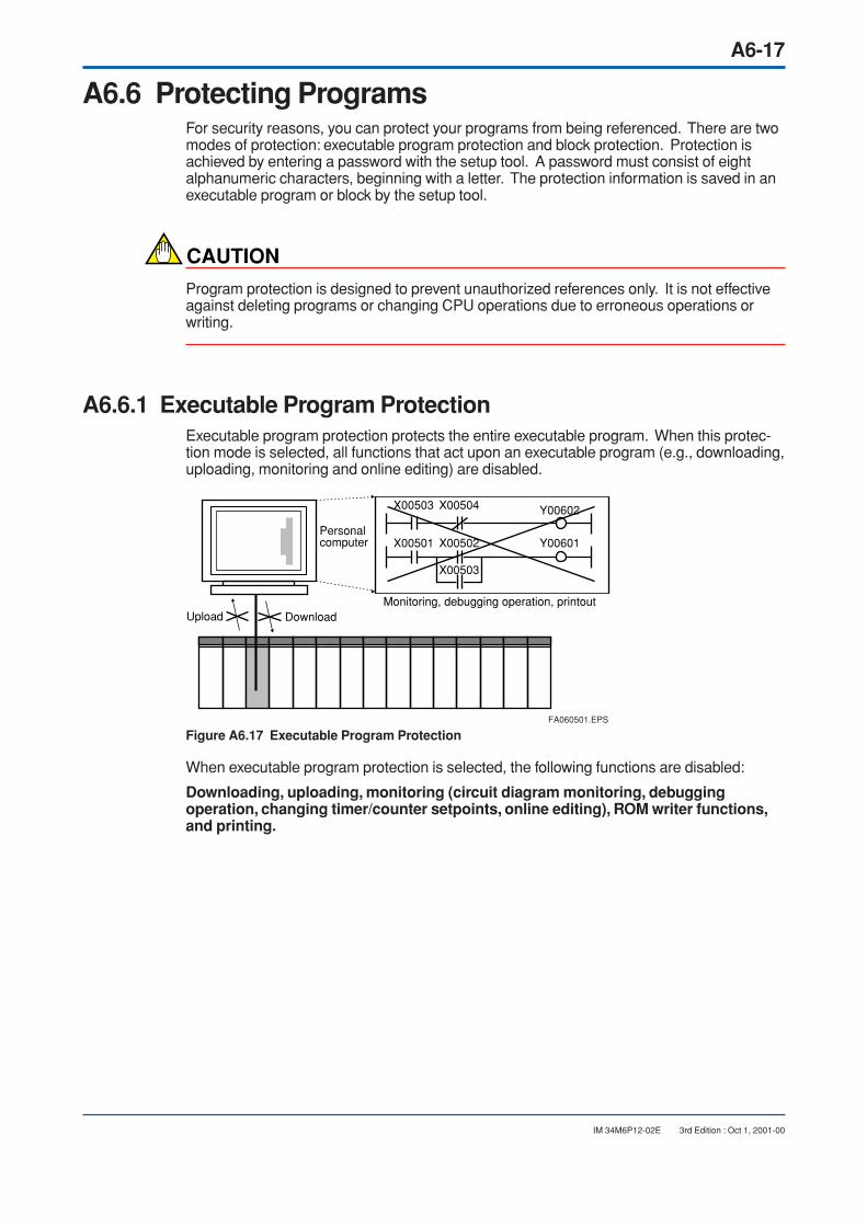
A6-17
IM 34M6P12-02E 3rd Edition : Oct 1, 2001-00
A6.6 Protecting ProgramsFor security reasons, you can protect your programs from being referenced. There are twomodes of protection: executable program protection and block protection. Protection isachieved by entering a password with the setup tool. A password must consist of eightalphanumeric characters, beginning with a letter. The protection information is saved in anexecutable program or block by the setup tool.
CAUTION
Program protection is designed to prevent unauthorized references only. It is not effectiveagainst deleting programs or changing CPU operations due to erroneous operations orwriting.
A6.6.1 Executable Program ProtectionExecutable program protection protects the entire executable program. When this protec-tion mode is selected, all functions that act upon an executable program (e.g., downloading,uploading, monitoring and online editing) are disabled.
Personalcomputer
X00503 X00504 Y00602
X00501 X00502
X00503
Y00601
Upload DownloadMonitoring, debugging operation, printout
FA060501.EPS
Figure A6.17 Executable Program Protection
When executable program protection is selected, the following functions are disabled:
Downloading, uploading, monitoring (circuit diagram monitoring, debuggingoperation, changing timer/counter setpoints, online editing), ROM writer functions,and printing.

A6-18
IM 34M6P12-02E 3rd Edition : Oct 1, 2001-00
A6.6.2 Block ProtectionBlock protection protects programs on a block-by-block basis. This protection mode isdesigned to prevent unauthorized references only. In addition, only specified blocks areincluded in the protection. When block protection is selected for a block, its circuit diagramsand instructions are not displayed on the programming tool.
Personalcomputer
X00503 X00504 Y00602
X00501 X00502
X00503
Y00601
Block n
Block m
The protection has the effectonly on specified blocks
FA060502.EPS
Figure A6.18 Block Protection
When block protection is selected, the following functions are disabled:
Monitoring (circuit diagram monitoring, debugging operation, changing timer/counter setpoints, online edit) and printing
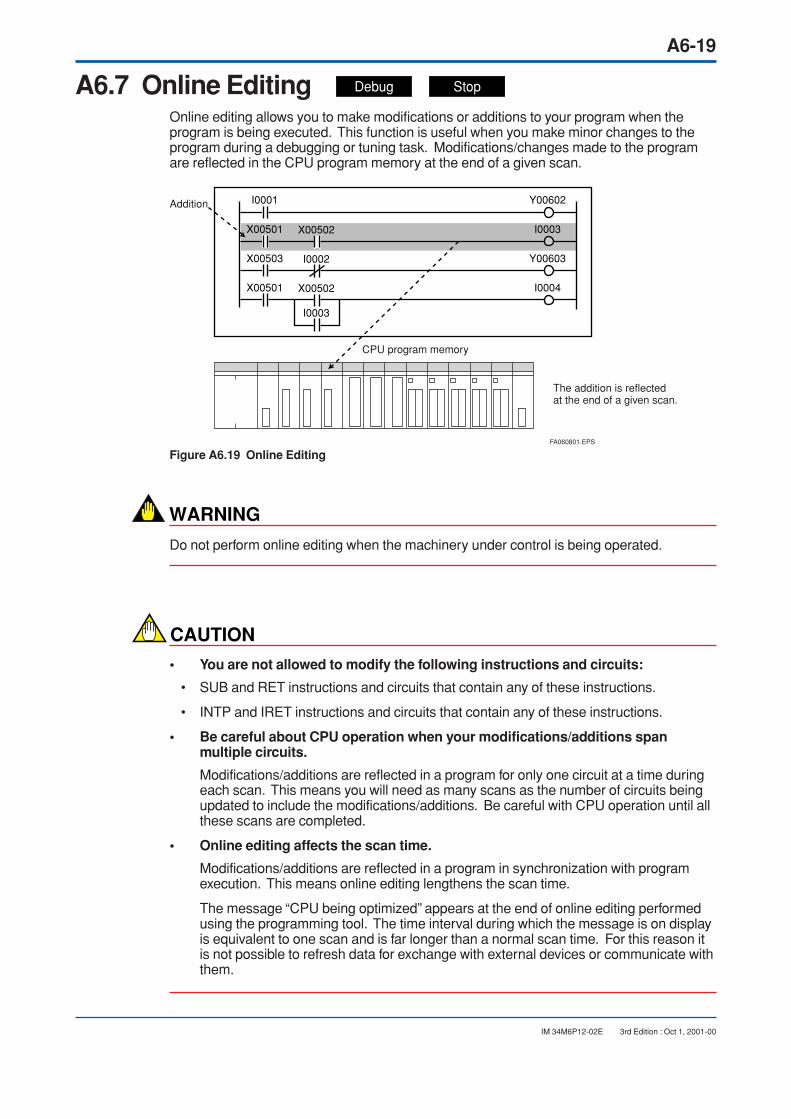
A6-19
IM 34M6P12-02E 3rd Edition : Oct 1, 2001-00
A6.7 Online EditingOnline editing allows you to make modifications or additions to your program when theprogram is being executed. This function is useful when you make minor changes to theprogram during a debugging or tuning task. Modifications/changes made to the programare reflected in the CPU program memory at the end of a given scan.
FA060801.EPS
CPU program memory
Addition
The addition is reflected at the end of a given scan.
I0001 Y00602
I0003
X00501 I0003X00502
X00503 Y00603I0002
X00501 I0004X00502
Figure A6.19 Online Editing
WARNING
Do not perform online editing when the machinery under control is being operated.
CAUTION
• You are not allowed to modify the following instructions and circuits:
• SUB and RET instructions and circuits that contain any of these instructions.
• INTP and IRET instructions and circuits that contain any of these instructions.
• Be careful about CPU operation when your modifications/additions spanmultiple circuits.
Modifications/additions are reflected in a program for only one circuit at a time duringeach scan. This means you will need as many scans as the number of circuits beingupdated to include the modifications/additions. Be careful with CPU operation until allthese scans are completed.
• Online editing affects the scan time.
Modifications/additions are reflected in a program in synchronization with programexecution. This means online editing lengthens the scan time.
The message “CPU being optimized” appears at the end of online editing performedusing the programming tool. The time interval during which the message is on displayis equivalent to one scan and is far longer than a normal scan time. For this reason itis not possible to refresh data for exchange with external devices or communicate withthem.
Debug Stop
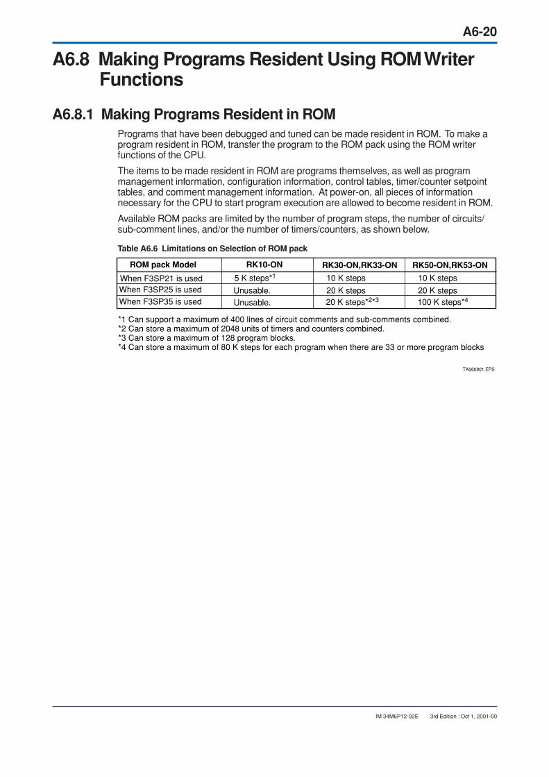
A6-20
IM 34M6P12-02E 3rd Edition : Oct 1, 2001-00
A6.8 Making Programs Resident Using ROM WriterFunctions
A6.8.1 Making Programs Resident in ROMPrograms that have been debugged and tuned can be made resident in ROM. To make aprogram resident in ROM, transfer the program to the ROM pack using the ROM writerfunctions of the CPU.
The items to be made resident in ROM are programs themselves, as well as programmanagement information, configuration information, control tables, timer/counter setpointtables, and comment management information. At power-on, all pieces of informationnecessary for the CPU to start program execution are allowed to become resident in ROM.
Available ROM packs are limited by the number of program steps, the number of circuits/sub-comment lines, and/or the number of timers/counters, as shown below.
Table A6.6 Limitations on Selection of ROM pack
ROM pack Model
TA060901.EPS
RK30-ON,RK33-ON RK50-ON,RK53-ON
When F3SP21 is usedWhen F3SP25 is usedWhen F3SP35 is used
RK10-ON
5 K steps*1 10 K steps
Unusable. 20 K stepsUnusable. 20 K steps*2*3
10 K steps
20 K steps100 K steps*4
*1 Can support a maximum of 400 lines of circuit comments and sub-comments combined.*2 Can store a maximum of 2048 units of timers and counters combined.*3 Can store a maximum of 128 program blocks.*4 Can store a maximum of 80 K steps for each program when there are 33 or more program blocks

A6-21
IM 34M6P12-02E 3rd Edition : Oct 1, 2001-00
With the configuration function, you can make the following two types of data resident inROM. These types of data are used to set initial values to be used by a program.
• Setpoints of 1,024 data registers’ worth of default data
• Either 32768 data registers’ or file registers’ worth of current values within CPUmodule-see subsection A6.8.2, “Setting Devices’ Current Values to Be Made Residentin ROM.”
At power-on, data read from the ROM pack is stored in data registers or file registersspecified with the configuration function. Data registers and file registers included in thedata retention in case of power failure revert to their respective default values. If you editboth of the configuration items mentioned above for the same data register, only thesetpoint of the second configuration item “Setting Devices’ Current Values” is effective.
TIP
Data retention in case of power failure is effective for devices not included in the configura-tion discussed above.
Making the initial setpoints of data registers resident in ROM is only possible when ModelRK30-0N, RK33-0N, RK50-0N or RK53-0N is selected as the ROM pack. Similarly, makingthe current values of data registers or file registers resident in ROM is only possible whenModel RK50-0N or RK53-0N is selected as the ROM pack.
If you perform both types of configuration mentioned above for the same data register, onlythe current value set by the latter type of configuration is effective.
TIP
Data retention in case of power failure is effective for devices not included in the configura-tion discussed above.
Program RAM configuration
Program management table
Program
Configuration table
I/O configuration table
Program control instructiontable
Timer/counter set valuetable
Utility
Program management table
Configuration table
I/O configuration table
Program control instructiontable
Timer/counter set valuetable
Device rangeOperation methods in case of an errorData lock-up ranges at a power failure
Lock-up/Not-lock-up type settingsSampling cyclesData code type
Jump Interrupt definitionsSubroutinesLabels
Timers and counters
Circuit comments, sub-comments or other information
Program ROM configuration
ROMblock
RAM
program Program
Utility
The program size is limited.
The data sizes are limited.
FA060901.EPS
Figure A6.20 Contents of Program to Be Made Resident in ROM

A6-22
IM 34M6P12-02E 3rd Edition : Oct 1, 2001-00
CAUTION
Be sure to debug and tune programs before making them resident in ROM. You cannot editor carry out partial modification of a program or data that has already been made residentin ROM. Programs made resident in ROM can only be executed on a CPU module whose“model name” has been transferred to the ROM pack.

A6-23
IM 34M6P12-02E 3rd Edition : Oct 1, 2001-00
A6.8.2 Setting Devices’ Current Values to Be Made Resident inROM
F3SP35F3SP25F3SP21
Define initial values to be made resident in data registers (D) or file registers (B) whenprogram execution begins. This definition is effective only when Model RK50-0N or RK53-0N is selected as the ROM pack.
The data items to be defined are the type of device, starting number, and quantity of de-vices. This configuration enables the current values of the specified devices to be stored inthe ROM pack when the “file-to-ROM transfer” or “CPU-to-ROM transfer (ROM copy)”function of the ROM writer functions is executed. You can determine whether or not toupdate the device data to be made resident in ROM with the current values when executingthe “file-to-ROM transfer” or “CPU-to-ROM transfer” function. When program executionbegins, the device data in the ROM pack is read and stored in the specified devices. Thisconfiguration is useful when you want to set a large volume of initial data or save initial datafor a program. You can set initial values in a maximum of 5120 data registers for theF3SP21 sequence CPU or a maximum of 32768 file registers for the F3SP25/F3SP35sequence CPUs.
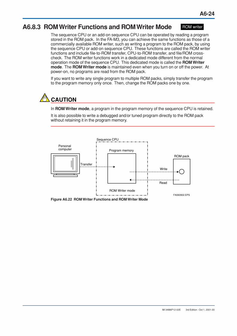
A6-24
IM 34M6P12-02E 3rd Edition : Oct 1, 2001-00
A6.8.3 ROM Writer Functions and ROM Writer Mode ROM writer
The sequence CPU or an add-on sequence CPU can be operated by reading a programstored in the ROM pack. In the FA-M3, you can achieve the same functions as those of acommercially available ROM writer, such as writing a program to the ROM pack, by usingthe sequence CPU or add-on sequence CPU. These functions are called the ROM writerfunctions and include file-to-ROM transfer, CPU-to-ROM transfer, and file/ROM cross-check. The ROM writer functions work in a dedicated mode different from the normaloperation mode of the sequence CPU. This dedicated mode is called the ROM Writermode. The ROM Writer mode is maintained even when you turn on or off the power. Atpower-on, no programs are read from the ROM pack.
If you want to write any single program to multiple ROM packs, simply transfer the programto the program memory only once. Then, change the ROM packs one by one.
CAUTION
In ROM Writer mode, a program in the program memory of the sequence CPU is retained.
It is also possible to write a debugged and/or tuned program directly to the ROM packwithout retaining it in the program memory.
Sequence CPU
FA060902.EPS
Transfer
Program memory
ROM Writer mode
Write
Read
ROM pack
Personalcomputer
Figure A6.22 ROM Writer Functions and ROM Writer Mode
A6-25
IM 34M6P12-02E 3rd Edition : Oct 1, 2001-00
Using the ROM writer functions, you can save a debugged and/or tuned program to theROM pack. To transfer the program to the ROM pack, use the ROM management functionof the programming tool. The following details the ROM writer functions.
File-to-ROM Transfer FunctionThis function writes a program or data to ROM.
It first transfers a program to the CPU’s program memory, and then writes the program toROM. At this point, you can determine whether or not to make the current values of de-vices resident in ROM (for the F3SP21, F3SP25 and F3SP35 only).
CPU-to-ROM Transfer (ROM Copy) FunctionThis function writes a program or data in the CPU directly to the ROM without transferring itusing the ROM management function of the programming tool. At this point, you candetermine whether or not to make the current values of devices resident in ROM.
A debugged and/or tuned program or data in the CPU is not initialized when the CPU ischanged to the ROM Writer mode. It is therefore possible to write the program or datadirectly to ROM. This function is also used to write the same program to multiple ROMpacks. You can write the program to all of the ROM packs by simply changing the ROMpacks one after another. There is no need to transfer the program repeatedly.
File/ROM Cross-check FunctionThis function cross checks the content of ROM with that of a program in WideField orLadder Diagram Support Program M3.
ROM Clearance FunctionThis function erases the content of a ROM.
CAUTION
• Change the CPU to ROM Writer mode before using the ROM writer functions. Youcannot use the ROM writer functions in other modes.
• Be sure to disable ROM Writer mode when you finish using the ROM writer functions.The CPU does not execute any sequencing functions if ROM Writer mode remainsactive.

A6-26
IM 34M6P12-02E 3rd Edition : Oct 1, 2001-00
A6.9 Exclusive Access RightAn exclusive access right is used to prevent a program, operation mode, or device datafrom being changed or prohibit the program or device data from being downloaded by otherusers when the program is being executed or debugged. Once you acquire the exclusiveaccess right, all alteration- and control-related commands entered from other tools, CPUmodules or personal computer links are rejected until you release the right.
If you withhold the exclusive access right, all alteration- and control-related commands fromother users remain disabled. Release the access right as soon as you have completed therequired process.
If another user has already acquired the exclusive access right, it is not available to you.
The exclusive access right is handled in the following three modes:
Acquisition
This mode acquires the exclusive access right.
Release
This mode releases the exclusive access right.
Forced Release
This mode permits you to forcibly release the exclusive access right from the CPU holdingthe right through access from a tool or module having no access right.
Personalcomputer
Obtains the exclusive access right.
Sequence CPU module
Personal computer link
Has no access.
FA061001.eps
Figure A6.22 Exclusive Access Right
Once the exclusive access right is acquired, the system prohibits the following acts frombeing performed by a tool or module having no access right:
CPU operation, CPU stop, debugging, downloading, debugging operation, use ofdebugging functions, writing to devices, and change in timer/counter setpoints.

A6-27
IM 34M6P12-02E 3rd Edition : Oct 1, 2001-00
A6.10 Sampling Trace Function F3SP35F3SP25
The sampling trace function sequentially stores the states and contents of devices selectedfor sampling, in the sampling trace memory of the sequence CPU.
The sampling trace function has three sampling modes:
• TRC-instruction sampling
• End-of-scan sampling
• Fixed-interval sampling
As the condition for triggering sampling, you can define the rising or falling edge of aselected relay signal or a match with the data of a selected word device. The CPU watchesthe trigger condition when processing the END instruction of a program. If the triggercondition becomes true, the CPU is allowed to perform 1024 rounds of sampling from apoint of time as much as the number of delays before (negative delay) or after (positivedelay) the condition becomes true.
Configure the sampling trace function using the programming tool. The results of samplingtrace operation can be viewed on the programming tool in timing-chart format, as shown onthe next page.
You can perform the sampling trace function in either the Run or Debug mode. The sam-pling trace function, if performed once again, deletes previous data. If you define samplingtrace function settings using the configuration function, the CPU begins sampling at themoment of power-on. If you define sampling trace function settings using the configurationfunction and then permanently store them in ROM, the CPU reverts to the ROM dataduring a power-on-and-off sequence even if you redefine the settings later using the pro-gramming tool.
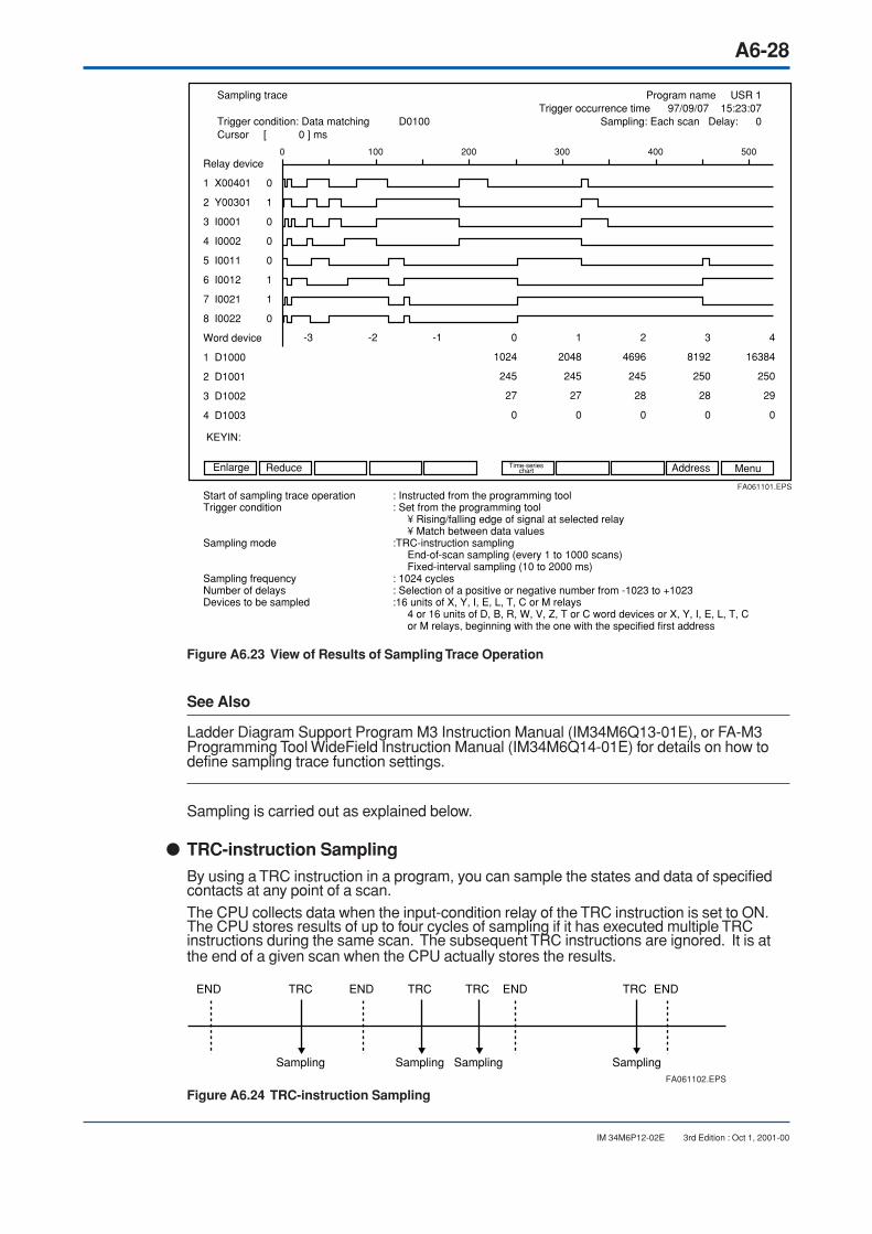
A6-28
IM 34M6P12-02E 3rd Edition : Oct 1, 2001-00
0 100 200 300 400 500
Sampling trace
Trigger condition: Data matching D0100Cursor [ 0 ] ms
Relay device
1
2
3
4
5
6
7
8
Word device
1
2
3
4
X00401
Y00301
I0001
I0002
I0011
I0012
I0021
I0022
D1000
D1001
D1002
D1003
0
1
0
0
0
1
1
0
Enlarge Reduce
Program name USR 1Trigger occurrence time 97/09/07 15:23:07
Sampling: Each scan Delay: 0
Time-serieschart Address Menu
1024
245
27
0
2048
245
27
0
4696
245
28
0
8192
250
28
0
16384
250
29
0
0 1 2-3 -2 -1 3 4
KEYIN:
Start of sampling trace operation : Instructed from the programming toolTrigger condition : Set from the programming tool
¥ Rising/falling edge of signal at selected relay ¥ Match between data values
Sampling mode :TRC-instruction sampling End-of-scan sampling (every 1 to 1000 scans) Fixed-interval sampling (10 to 2000 ms)
Sampling frequency : 1024 cyclesNumber of delays : Selection of a positive or negative number from -1023 to +1023Devices to be sampled :16 units of X, Y, I, E, L, T, C or M relays
4 or 16 units of D, B, R, W, V, Z, T or C word devices or X, Y, I, E, L, T, C or M relays, beginning with the one with the specified first address
FA061101.EPS
Figure A6.23 View of Results of Sampling Trace Operation
See Also
Ladder Diagram Support Program M3 Instruction Manual (IM34M6Q13-01E), or FA-M3Programming Tool WideField Instruction Manual (IM34M6Q14-01E) for details on how todefine sampling trace function settings.
Sampling is carried out as explained below.
TRC-instruction SamplingBy using a TRC instruction in a program, you can sample the states and data of specifiedcontacts at any point of a scan.The CPU collects data when the input-condition relay of the TRC instruction is set to ON.The CPU stores results of up to four cycles of sampling if it has executed multiple TRCinstructions during the same scan. The subsequent TRC instructions are ignored. It is atthe end of a given scan when the CPU actually stores the results.
Sampling
TRCEND END END ENDTRC TRC TRC
Sampling Sampling SamplingFA061102.EPS
Figure A6.24 TRC-instruction Sampling
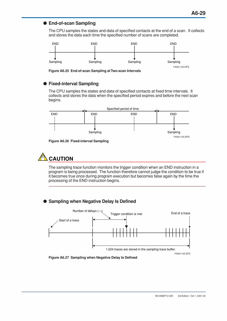
A6-29
IM 34M6P12-02E 3rd Edition : Oct 1, 2001-00
End-of-scan Sampling
The CPU samples the states and data of specified contacts at the end of a scan. It collectsand stores the data each time the specified number of scans are completed.
Sampling
END END END END
Sampling Sampling Sampling
FA061103.EPS
Figure A6.25 End-of-scan Sampling at Two-scan Intervals
Fixed-interval Sampling
The CPU samples the states and data of specified contacts at fixed time intervals. Itcollects and stores the data when the specified period expires and before the next scanbegins.
END END
Sampling Sampling
END END
Specified period of time
FA061104.EPS
Figure A6.26 Fixed-interval Sampling
CAUTION
The sampling trace function monitors the trigger condition when an END instruction in aprogram is being processed. The function therefore cannot judge the condition to be true ifit becomes true once during program execution but becomes false again by the time theprocessing of the END instruction begins.
Sampling when Negative Delay Is Defined
Number of delays (—)
Start of a trace
Trigger condition is met End of a trace
1,024 traces are stored in the sampling trace buffer.FA061105.EPS
Figure A6.27 Sampling when Negative Delay Is Defined

A6-30
IM 34M6P12-02E 3rd Edition : Oct 1, 2001-00
Sampling when Positive Delay Is Defined
Number of delays (+)
Start of a trace
Trigger condition is met End of a trace
1,024 traces are stored inthe sampling trace buffer.
FA061106.EPS
Figure A6.28 Sampling when Positive Delay Is Defined

A6-31
IM 34M6P12-02E 3rd Edition : Oct 1, 2001-00
A6.11 Personal Computer Link Function F3SP35F3SP25F3SP21
The programming tool connector on the front of the CPU module functions in the same wayas the RS-232-C communication port on the F3LC11-1N personal computer link module.This means you can connect a host computer, such as a personal computer or FA com-puter, or a monitor to the CPU module to perform one-to-one communication as with thepersonal computer link module. This feature is called the personal computer link function.
You can monitor and configure devices and start, stop, load and save programs by enteringcommands from the host computer.
X00503 X00504 Y00602
X00501 X00502
X00503
Y00601
Personal computeror monitor with aPC interface
Personal computerlink function
Personal computeron which "LadderDiagram SupportProgram M3" runs
Sequence CPU module
Programming toolconnection function
Personalcomputer
FA061201.EPS
*Refers to either WideField or Loadder Diagram Support Program M3
Figure A6.29 Personal Computer Link Function

A6-32
IM 34M6P12-02E 3rd Edition : Oct 1, 2001-00
A6.11.1 System ConfigurationFigure A6.30 shows examples of system configuration using the personal computer linkfunction.
External equipment, such as a personal computer or monitor, is connected to the CPUmodule of the FA-M3 by using the programming tool connector on the front of the FA-M3and a dedicated programming tool cable.
Personalcomputer Monitor
Personal computer link cable
Sequence CPU module Sequence CPU module
Personal computer link cable
FA061202.EPS
Figure A6.30 Examples of Connection between CPU Module and External Equipment
For conformance to CE Marking, fit a ferrite core to the cable for the programming tools forequipment using the personal computer link functions.
Kitagawa Industries Co., Ltd. RFC series
Examples of ferrite core TDK Corporation ZCAT series
Tokin Corporation ESD-SR series
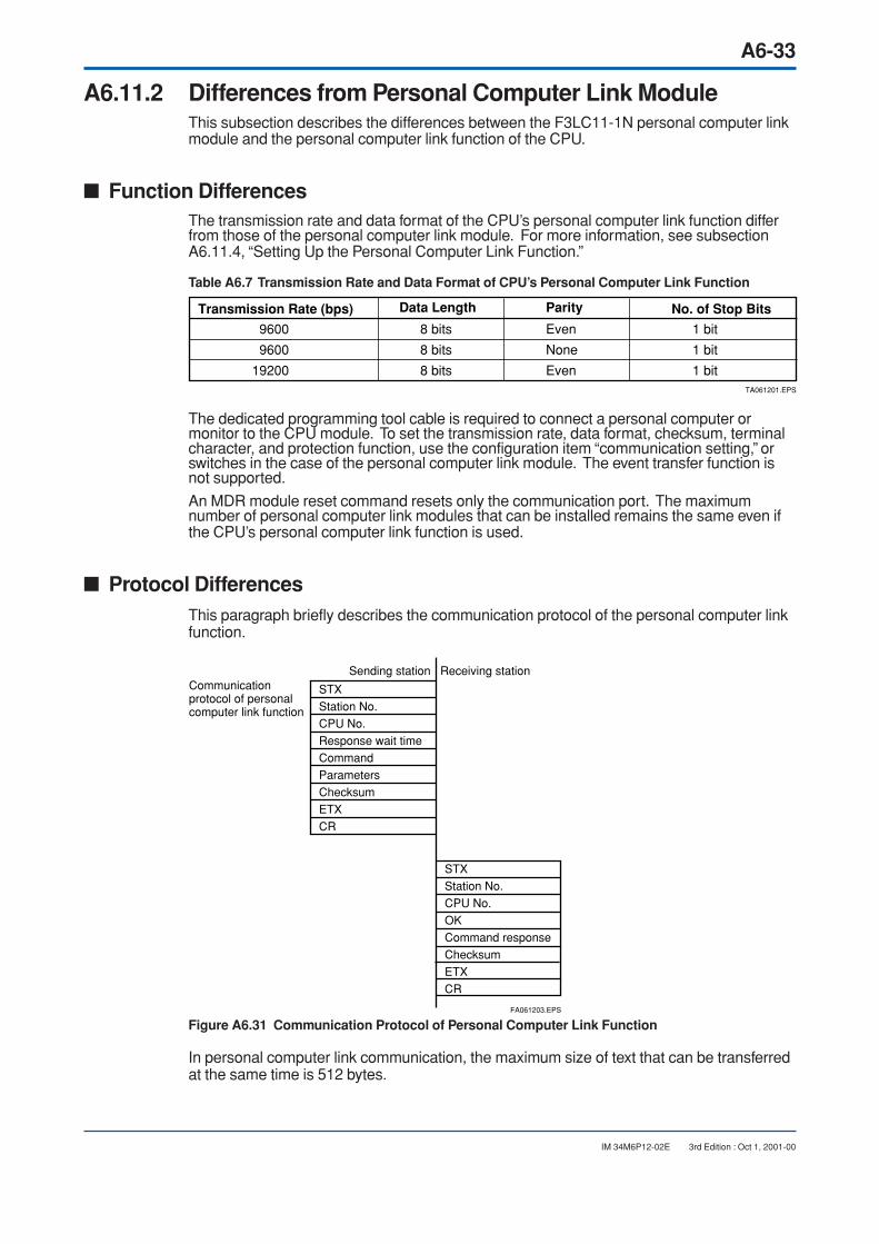
A6-33
IM 34M6P12-02E 3rd Edition : Oct 1, 2001-00
A6.11.2 Differences from Personal Computer Link ModuleThis subsection describes the differences between the F3LC11-1N personal computer linkmodule and the personal computer link function of the CPU.
Function DifferencesThe transmission rate and data format of the CPU’s personal computer link function differfrom those of the personal computer link module. For more information, see subsectionA6.11.4, “Setting Up the Personal Computer Link Function.”
Table A6.7 Transmission Rate and Data Format of CPU’s Personal Computer Link Function
9600
9600
19200
8 bits
8 bits
8 bits
Even
None
EvenTA061201.EPS
1 bit
1 bit
1 bit
Transmission Rate (bps) Data Length Parity No. of Stop Bits
The dedicated programming tool cable is required to connect a personal computer ormonitor to the CPU module. To set the transmission rate, data format, checksum, terminalcharacter, and protection function, use the configuration item “communication setting,” orswitches in the case of the personal computer link module. The event transfer function isnot supported.
An MDR module reset command resets only the communication port. The maximumnumber of personal computer link modules that can be installed remains the same even ifthe CPU’s personal computer link function is used.
Protocol DifferencesThis paragraph briefly describes the communication protocol of the personal computer linkfunction.
STX
Station No.
CPU No.
Response wait time
Command
Parameters
Checksum
ETX
CR
STX
Station No.
CPU No.
OK
Command response
Checksum
ETX
CR
Communication protocol of personalcomputer link function
Sending station Receiving station
FA061203.EPS
Figure A6.31 Communication Protocol of Personal Computer Link Function
In personal computer link communication, the maximum size of text that can be transferredat the same time is 512 bytes.
A6-34
IM 34M6P12-02E 3rd Edition : Oct 1, 2001-00
A6.11.3 Specification of Personal Computer Link FunctionTable A6.8 summarizes the specifications of the CPU’s personal computer link function.
Table A6.8 Specifications of Personal Computer Link Function
TA061202.EPS
Item Description Setup*1
Interface
Supported CPUs F3SP21-0N , F3SP25-2N , F3SP35-5N
Compliant with EIA RS-232C
Transmission mode Half-duplexSynchronization Start-stop
Transmission rate(bps) 9600/19200
Data format
Start bit : 1
Data length: Fixed at 8 bits
Parity bit : None/Even
Stop bit : Fixed at 1 bit
Error checking Parity check
Checksum : Yes/NoRS-232-C control line Not used.
Xon/Xoff Not used.
Configurable item Transmission rate, data format, checksum, terminalcharacter, and protection function
Protocol Dedicated protocol
Terminating character Yes/No
Protection function*2 Yes/No
Range of accessoperations
Transmission distance 8 m max.
External connection Dedicated cable
Access to all control data, uploading/downloading ladder programs, CPU operation (Run mode)/stop (Stop mode), and reading error logs
*1 The check mark indicates that the user can configure the item by using the configuration function. However, there are restrictions on the way the transmission rate and parity check are combined. See subsection A6.11.4, "Setting Up the Personal Computer Link Function," for more information.
*2 You can set the protection function to the Yes option to prevent inadvertent writing to the FA-M3.
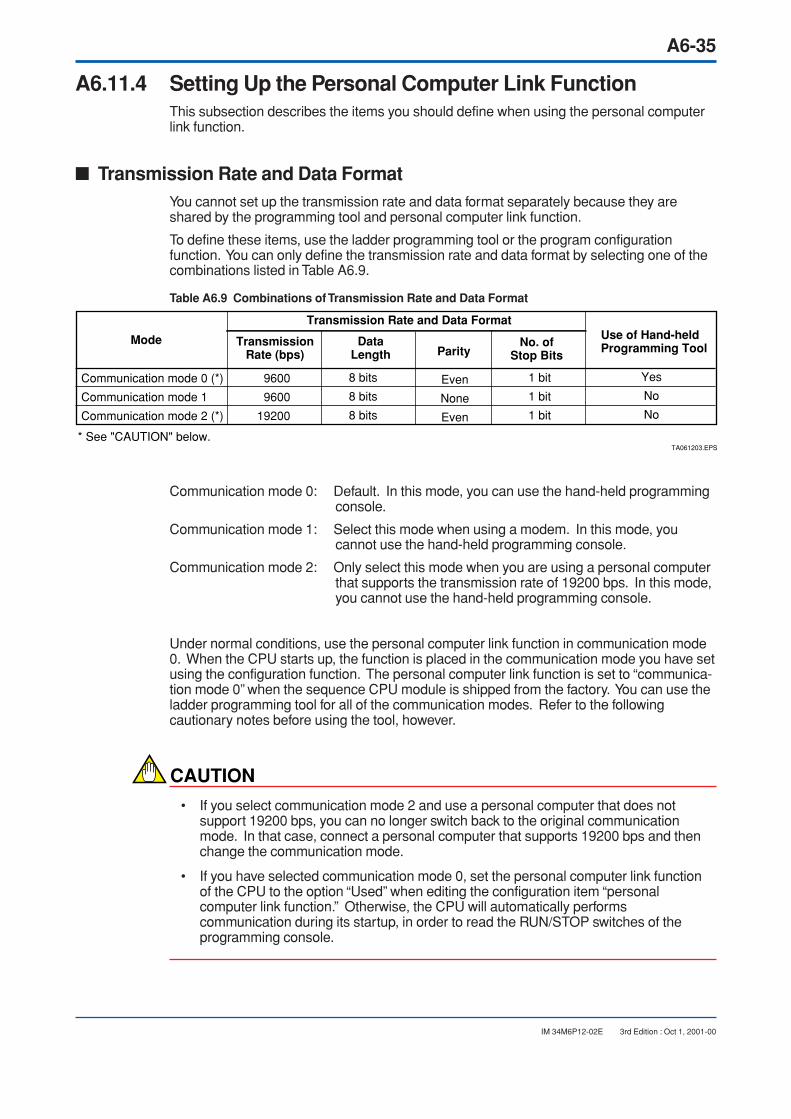
A6-35
IM 34M6P12-02E 3rd Edition : Oct 1, 2001-00
A6.11.4 Setting Up the Personal Computer Link FunctionThis subsection describes the items you should define when using the personal computerlink function.
Transmission Rate and Data FormatYou cannot set up the transmission rate and data format separately because they areshared by the programming tool and personal computer link function.
To define these items, use the ladder programming tool or the program configurationfunction. You can only define the transmission rate and data format by selecting one of thecombinations listed in Table A6.9.
Table A6.9 Combinations of Transmission Rate and Data Format
TA061203.EPS
Mode
Transmission Rate and Data Format
TransmissionRate (bps)
DataLength Parity
No. ofStop Bits
Use of Hand-heldProgramming Tool
Communication mode 0 (*)
Communication mode 1
Communication mode 2 (*)
9600
9600
19200
8 bits
8 bits
8 bits
Even
None
Even
1 bit
1 bit
1 bit
Yes
No
No
* See "CAUTION" below.
Communication mode 0: Default. In this mode, you can use the hand-held programmingconsole.
Communication mode 1: Select this mode when using a modem. In this mode, youcannot use the hand-held programming console.
Communication mode 2: Only select this mode when you are using a personal computerthat supports the transmission rate of 19200 bps. In this mode,you cannot use the hand-held programming console.
Under normal conditions, use the personal computer link function in communication mode0. When the CPU starts up, the function is placed in the communication mode you have setusing the configuration function. The personal computer link function is set to “communica-tion mode 0” when the sequence CPU module is shipped from the factory. You can use theladder programming tool for all of the communication modes. Refer to the followingcautionary notes before using the tool, however.
CAUTION
• If you select communication mode 2 and use a personal computer that does notsupport 19200 bps, you can no longer switch back to the original communicationmode. In that case, connect a personal computer that supports 19200 bps and thenchange the communication mode.
• If you have selected communication mode 0, set the personal computer link functionof the CPU to the option “Used” when editing the configuration item “personalcomputer link function.” Otherwise, the CPU will automatically performscommunication during its startup, in order to read the RUN/STOP switches of theprogramming console.
A6-36
IM 34M6P12-02E 3rd Edition : Oct 1, 2001-00
CAUTION
• Be careful when setting the transmission rate.
The WideField supports all of the communication modes listed on the previous page.However, first refer to the instruction manual of the personal computer that runs theWideField to check available transmission rates and data formats. Then, temporarilychange the transmission rate of the personal computer link function using theprogramming tool to make sure the CPU module can communicate with the personalcomputer in the communication mode you want to use. Finally, configure the personalcomputer link function according to that communication mode. Note that the personalcomputer link function automatically reverts to the previous transmission rate ifcommunication is not established after a temporary change in the transmission rate.
If you select a communication mode in which the personal computer cannotcommunicate, it is impossible to communicate with the CPU module through thecomputer. If this happens, first install the sequence CPU module in the fifth or highernumbered slot of the main unit. Next, turn on the power and make sure the RDYindicator has come on. Then, turn off the power to clear the CPU memory completelyand allow the CPU module to revert to its factory-set defaults.
CAUTION
• To use the personal computer link function, set the configuration item “personalcomputer link function” to the option “Used.” If you do not select this option, the CPUperforms communication at power-on in order to recognize the hand-heldprogramming console. Consequently, you may fail to successfully communicate withhigher-order equipment.
• If you set the configuration item “personal computer link function” to the option “Used,”the settings of the RUN/STOP switches of the hand-held programming console are notput into effect.
Checksum, Terminal Character and Write Protection FunctionDefine these items using the program configuration item “communication setting.” Bydefault, all these items are set to the option “Not used.”
SEE ALSO
FA-M3 Programming Tool WideField Instruction Manual (IM34M6Q14-01E), or LadderDiagram Support Program M3 Instruction Manual (IM34M6Q13-01E), for details on how touse the configuration function.
A6-37
IM 34M6P12-02E 3rd Edition : Oct 1, 2001-00
A6.11.5 Communication ProcedureTo be able to perform communication, the transmission specifications, e.g., the transmis-sion rate and data format, must be consistent between the CPU module and a personalcomputer, FA computer or monitor.
Use the program configuration function to set up the transmission specifications of thesequence CPU module. To set the transmission specifications of a personal computer orFA computer, use a communication software program. In the case of the transmissionspecifications of a monitor, use the configuration function of the monitor itself.
Communication ProcedureThe following outlines the procedure of communication using a BASIC program on apersonal computer. For details on the statements and functions used in the program, referto the BASIC reference manual that came with your personal computer.
1. Open the RS-232-C communication file.
Enter a command in the following format:
OPEN “COM: xxxxx” AS#y
xxxxx: Enter communication parameters, such as the parity, data length, and thenumber of stop bits.
y: File number. This number is used for subsequent inputs to and outputs fromthe file.
2. Send a command to the FA-M3 in the following format.
PRINT#y, String variable name (or string)
3. Enter a command in the following format to receive a response from the FA-M3.
LINE INPUT#y, String variable name
INPUT#y, String variable name
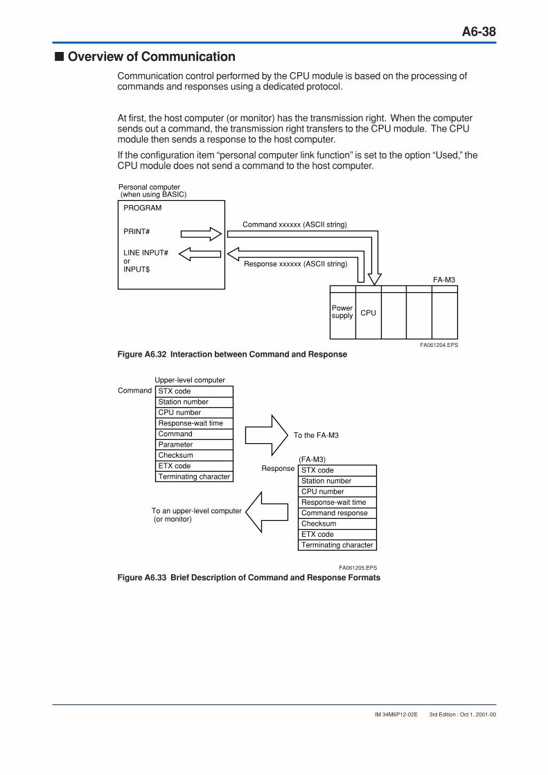
A6-38
IM 34M6P12-02E 3rd Edition : Oct 1, 2001-00
Overview of CommunicationCommunication control performed by the CPU module is based on the processing ofcommands and responses using a dedicated protocol.
At first, the host computer (or monitor) has the transmission right. When the computersends out a command, the transmission right transfers to the CPU module. The CPUmodule then sends a response to the host computer.
If the configuration item “personal computer link function” is set to the option “Used,” theCPU module does not send a command to the host computer.
Personal computer (when using BASIC)
PROGRAM
PRINT#
LINE INPUT#orINPUT$
Command xxxxxx (ASCII string)
Response xxxxxx (ASCII string)
Powersupply CPU
FA-M3
FA061204.EPS
Figure A6.32 Interaction between Command and Response
STX code
Station number
CPU number
Response-wait time
Command
Parameter
Checksum
ETX code
Terminating characterSTX code
Station number
CPU number
Response-wait time
Command response
Checksum
ETX code
Terminating character
CommandUpper-level computer
To an upper-level computer (or monitor)
Response
To the FA-M3
(FA-M3)
FA061205.EPS
Figure A6.33 Brief Description of Command and Response Formats
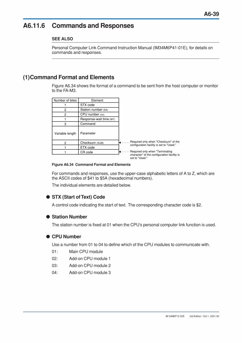
A6-39
IM 34M6P12-02E 3rd Edition : Oct 1, 2001-00
A6.11.6 Commands and Responses
SEE ALSO
Personal Computer Link Command Instruction Manual (IM34M6P41-01E), for details oncommands and responses.
(1)Command Format and ElementsFigure A6.34 shows the format of a command to be sent from the host computer or monitorto the FA-M3.
STX code
Station number (SA)
CPU number (nn)
Response-wait time (WT)
Command
Parameter
Checksum (SUM)
ETX code
CR code
Required only when "Checksum" of the configuration facility is set to "Used."
Required only when "Terminating character" of the configuration facility is set to "Used."
Number of bites
1
2
2
1
3
Variable length
2
1
1
Element
Figure A6.34 Command Format and Elements
For commands and responses, use the upper-case alphabetic letters of A to Z, which arethe ASCII codes of $41 to $5A (hexadecimal numbers).
The individual elements are detailed below.
STX (Start of Text) Code
A control code indicating the start of text. The corresponding character code is $2.
Station Number
The station number is fixed at 01 when the CPU’s personal computer link function is used.
CPU Number
Use a number from 01 to 04 to define which of the CPU modules to communicate with.
01: Main CPU module
02: Add-on CPU module 1
03: Add-on CPU module 2
04: Add-on CPU module 3
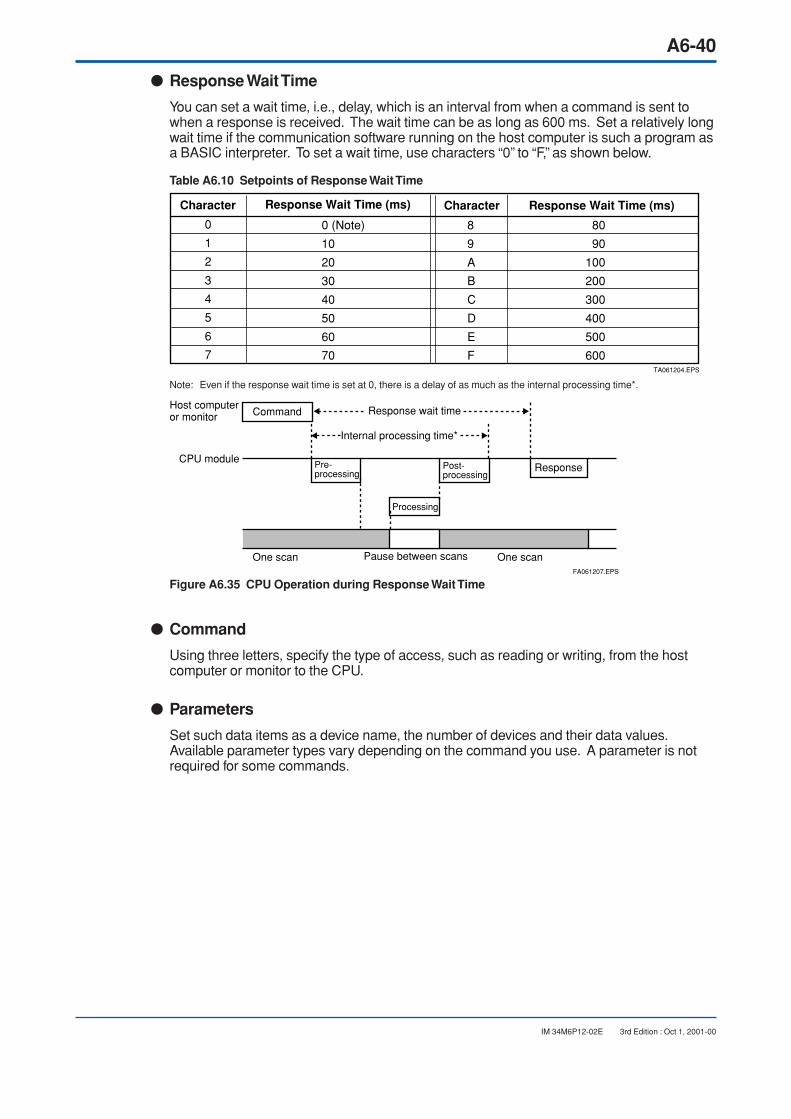
A6-40
IM 34M6P12-02E 3rd Edition : Oct 1, 2001-00
Response Wait Time
You can set a wait time, i.e., delay, which is an interval from when a command is sent towhen a response is received. The wait time can be as long as 600 ms. Set a relatively longwait time if the communication software running on the host computer is such a program asa BASIC interpreter. To set a wait time, use characters “0” to “F,” as shown below.
Table A6.10 Setpoints of Response Wait Time
TA061204.EPS
Character Response Wait Time (ms) Character Response Wait Time (ms)
0 (Note)
10
20
30
40
50
60
70
0
1
2
3
4
5
6
7
8
9
A
B
C
D
E
F
80
90
100
200
300
400
500
600
Note: Even if the response wait time is set at 0, there is a delay of as much as the internal processing time*.
Host computeror monitor Command
CPU module
Response wait time
Internal processing time*
Pre-processing
Response
One scan One scan Pause between scansFA061207.EPS
Post-processing
Processing
Figure A6.35 CPU Operation during Response Wait Time
Command
Using three letters, specify the type of access, such as reading or writing, from the hostcomputer or monitor to the CPU.
Parameters
Set such data items as a device name, the number of devices and their data values.Available parameter types vary depending on the command you use. A parameter is notrequired for some commands.
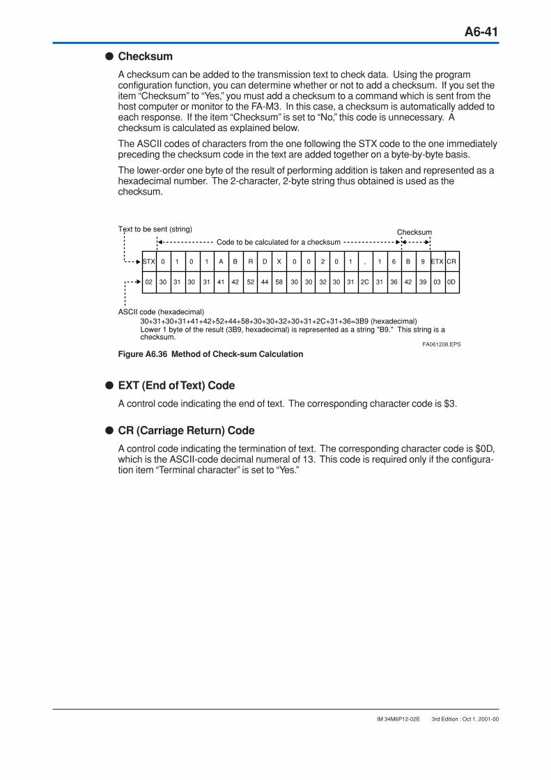
A6-41
IM 34M6P12-02E 3rd Edition : Oct 1, 2001-00
Checksum
A checksum can be added to the transmission text to check data. Using the programconfiguration function, you can determine whether or not to add a checksum. If you set theitem “Checksum” to “Yes,” you must add a checksum to a command which is sent from thehost computer or monitor to the FA-M3. In this case, a checksum is automatically added toeach response. If the item “Checksum” is set to “No,” this code is unnecessary. Achecksum is calculated as explained below.
The ASCII codes of characters from the one following the STX code to the one immediatelypreceding the checksum code in the text are added together on a byte-by-byte basis.
The lower-order one byte of the result of performing addition is taken and represented as ahexadecimal number. The 2-character, 2-byte string thus obtained is used as thechecksum.
30+31+30+31+41+42+52+44+58+30+30+32+30+31+2C+31+36=3B9 (hexadecimal)Lower 1 byte of the result (3B9, hexadecimal) is represented as a string "B9." This string is a checksum.
Text to be sent (string)
ASCII code (hexadecimal)
Code to be calculated for a checksumChecksum
STX 0 1 0 1 A B R D X 0 0 2 1 6 B0 1 , 9 ETX CR
02 30 31 30 31 41 42 52 44 58 30 30 32 31 36 4230 31 2C 39 03 0D
FA061208.EPS
Figure A6.36 Method of Check-sum Calculation
EXT (End of Text) Code
A control code indicating the end of text. The corresponding character code is $3.
CR (Carriage Return) Code
A control code indicating the termination of text. The corresponding character code is $0D,which is the ASCII-code decimal numeral of 13. This code is required only if the configura-tion item “Terminal character” is set to “Yes.”
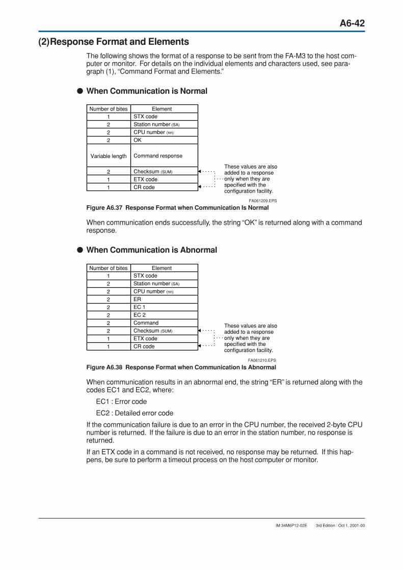
A6-42
IM 34M6P12-02E 3rd Edition : Oct 1, 2001-00
(2)Response Format and ElementsThe following shows the format of a response to be sent from the FA-M3 to the host com-puter or monitor. For details on the individual elements and characters used, see para-graph (1), “Command Format and Elements.”
When Communication is Normal
STX code
Station number (SA)
CPU number (nn)
OK
Command response
Checksum (SUM)
ETX code
CR code
Number of bites
1
2
2
2
Variable length
2
1
1
Element
These values are alsoadded to a responseonly when they arespecified with theconfiguration facility.
FA061209.EPS
Figure A6.37 Response Format when Communication Is Normal
When communication ends successfully, the string “OK” is returned along with a commandresponse.
When Communication is Abnormal
STX code
Station number (SA)
CPU number (nn)
ER
EC 1
EC 2
Command
Checksum (SUM)
ETX code
CR code
Number of bites
1
2
2
2
2
2
2
2
1
1
Element
These values are alsoadded to a responseonly when they arespecified with theconfiguration facility.
FA061210.EPS
Figure A6.38 Response Format when Communication Is Abnormal
When communication results in an abnormal end, the string “ER” is returned along with thecodes EC1 and EC2, where:
EC1 : Error code
EC2 : Detailed error code
If the communication failure is due to an error in the CPU number, the received 2-byte CPUnumber is returned. If the failure is due to an error in the station number, no response isreturned.
If an ETX code in a command is not received, no response may be returned. If this hap-pens, be sure to perform a timeout process on the host computer or monitor.

A6-43
IM 34M6P12-02E 3rd Edition : Oct 1, 2001-00
(3)Error Code in a ResponseA communication failure may occur when the sequence CPU module receives a command.In that case, the module returns the string “ER” and an error code as a response to thecommand.
The following error codes are reserved.
Table A6.11 Error Codes
Error Code (EC1) Probable Cause
TA0601205.EPS
Meaning
CPU number error - The CPU number is outside the range of 1 to 4.Command error - The command does not exist.
- The command is not executable.
Device specification error- The device name does not exist.*- Incorrectly specified the bit devices in an attempt to read/write them in units of words.
Value outside the range
- Attempted to use characters other than 0 and 1 when setting bits.*- Attempted to use values other than 0000 to FFFF when setting words.- The starting point in the command, such as Load or Save, is outside the range of addresses.
Number of data itemsoutside the range
- The number of bits or words is outside the specified range.*- The specified number of data items does not match the number of parameters including device names.
Monitor error- Attempted to execute monitoring without having specified a monitor command (BRS or WRS).
Parameter error - The parameter is incorrect for a reason other than noted above.*
Communication error - An error has occurred during communication.*Checksum error - The check sum is wrong due to missing bits, garbled character,etc.
Internal buffer overflow - The amount of data received is larger than the specified.
Timeout - No end-of-process response is returned from the CPU for reasons such as a CPU power failure.
CPU processing failure - The CPU has detected an error when processing the command.
Internal error- A Cancel command (PLC) has been issued while neither a Load command (PLD) nor a Save command (PSV) is in process.- An internal error is found.
* See Table 6.12, "Detailed Error Codes," for more information.
0102
03
04
05
06
08
41
42
43
51
52
F1
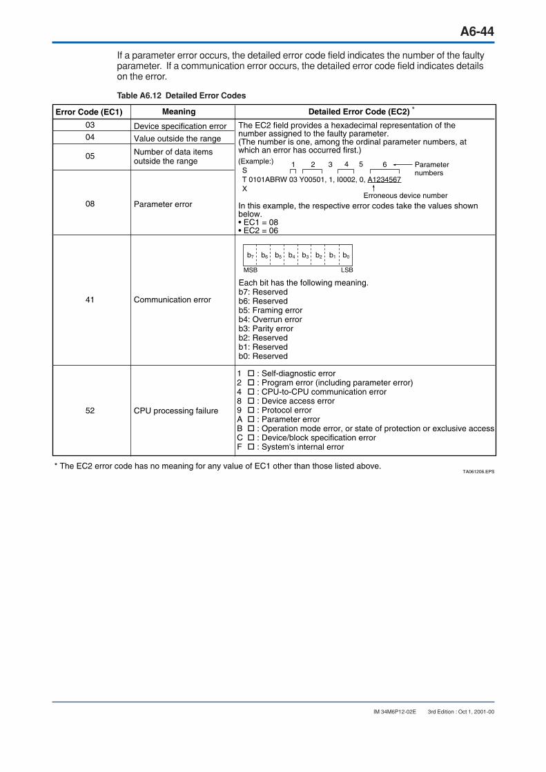
A6-44
IM 34M6P12-02E 3rd Edition : Oct 1, 2001-00
If a parameter error occurs, the detailed error code field indicates the number of the faultyparameter. If a communication error occurs, the detailed error code field indicates detailson the error.
Table A6.12 Detailed Error Codes
Error Code (EC1) Detailed Error Code (EC2)
TA061206.EPS
Meaning
03
04
05
08
41
52
(Example:) S T 0101ABRW 03 Y00501, 1, I0002, 0, A1234567 X
1 2 43 65 Parameternumbers
Erroneous device number
b7 b6 b5 b4 b3 b2 b1 b0
LSB
Device specification error The EC2 field provides a hexadecimal representation of thenumber assigned to the faulty parameter.(The number is one, among the ordinal parameter numbers, at which an error has occurred first.)
In this example, the respective error codes take the values shownbelow.• EC1 = 08• EC2 = 06
Value outside the range
Number of data itemsoutside the range
Parameter error
Communication error
MSB
Each bit has the following meaning.b7: Reservedb6: Reservedb5: Framing errorb4: Overrun errorb3: Parity errorb2: Reservedb1: Reservedb0: Reserved
CPU processing failure
1 : Self-diagnostic error2 : Program error (including parameter error)4 : CPU-to-CPU communication error8 : Device access error9 : Protocol errorA : Parameter errorB : Operation mode error, or state of protection or exclusive accessC : Device/block specification errorF : System's internal error
* The EC2 error code has no meaning for any value of EC1 other than those listed above.
*
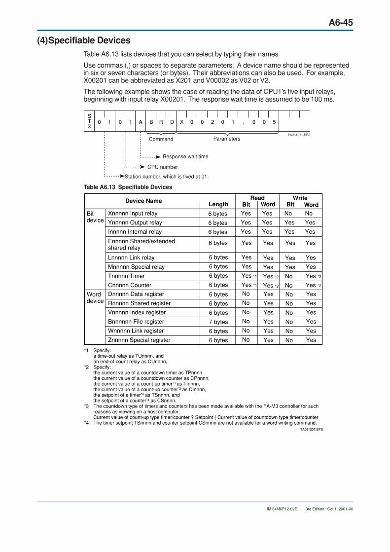
A6-45
IM 34M6P12-02E 3rd Edition : Oct 1, 2001-00
(4)Specifiable DevicesTable A6.13 lists devices that you can select by typing their names.
Use commas (,) or spaces to separate parameters. A device name should be representedin six or seven characters (or bytes). Their abbreviations can also be used. For example,X00201 can be abbreviated as X201 and V00002 as V02 or V2.
The following example shows the case of reading the data of CPU1’s five input relays,beginning with input relay X00201. The response wait time is assumed to be 100 ms.
FA061211.EPS
STX
0 1 0 0 0 2 0 1 0 0 5,1 A B R D X
Command Parameters
Response wait time
CPU number
Station number, which is fixed at 01.
Table A6.13 Specifiable Devices
Device Name Write
TA061207.EPS
ReadLength WordBit WordBit
Bitdevice
Worddevice
Lnnnnn Link relay
Mnnnnn Special relay
Tnnnnn Timer
Cnnnnn Counter
Xnnnnn Input relay
Ynnnnn Output relay
Innnnn Internal relay
Ennnnn Shared/extendedshared relay
Dnnnnn Data register
Rnnnnn Shared register
Vnnnnn Index register
Bnnnnnn File register
Wnnnnn Link register
Znnnnn Special register
6 bytes
6 bytes
6 bytes
7 bytes
6 bytes
6 bytes
6 bytes
6 bytes
6 bytes
6 bytes
6 bytes
6 bytes
6 bytes
6 bytes
Yes
Yes
Yes
Yes
Yes
Yes
No
Yes
Yes
No
Yes
Yes
Yes Yes Yes Yes
Yes
Yes
Yes *1
Yes *1
Yes
Yes
Yes *2
Yes *2
Yes
Yes
No
No
Yes
Yes
Yes *2
Yes *2
No
No
No
No
No
No
Yes
Yes
Yes
Yes
Yes
Yes
No
No
No
No
No
No
Yes
Yes
Yes
Yes
Yes
Yes
*1 Specify:a time-out relay as TUnnnn, andan end-of-count relay as CUnnnn,
*2 Specify:the current value of a countdown timer as TPnnnn,the current value of a countdown counter as CPnnnn,the current value of a count-up timer*3 as TInnnn,the current value of a count-up counter*3 as CInnnn,the setpoint of a timer*4 as TSnnnn, andthe setpoint of a counter*4 as CSnnnn.
*3 The countdown type of timers and counters has been made available with the FA-M3 controller for such reasons as viewing on a host computer.Current value of count-up type timer/counter ? Setpoint ( Current value of countdown type timer/counter
*4 The timer setpoint TSnnnn and counter setpoint CSnnnn are not available for a word writing command.
A6-46
IM 34M6P12-02E 3rd Edition : Oct 1, 2001-00
(5)Cautionary Notes on Communication Process• No response may be returned if, for exanple, you specify a wrong station number in a
command. In such a case, perform a time - out process on the host computer.
• When downloading a program using the personal computer link function, you are notallowed to download the program at the same time using a personal computer linkmodule or Ethernet interface module. If you do, normal operation is not guaranteed.
• If you write a value to a shared device that is being used by another CPU, the writtenvalue may soon be updated.
• If you are using a monitoring-purpose command, you must renew it in the event of apower failure.
• In personal computer link communication, the maximum size of text that can be sentor received by the CPU module at one time is 512 bytes. The maximum size that canbe received by the host computer may be limited to 256 bytes if there is such alimitation on the computer. If this is the case, pay special regard to the length ofresponse text. Take such corrective measures as reducing the number of devices tobe read, so that the text length will not exceed 256 bytes.
A6-47
IM 34M6P12-02E 3rd Edition : Oct 1, 2001-00
A6.12 Device Management FunctionThe device management function enables you to upload/download device information/dataof the CPU module to/from the programming tool*, edit the data, and cross-check it againstthe CPU module and the programming tool. You can specify the range of devices whosedata are uploaded or downloaded. You can also use this function to set defaults in deviceswhen, for example, replacing the CPU module.
* WideField or Ladder Diagram Support Program M3.
The devices that you can configure using the device management function are:
internal relays (I), shared relays (E), time-out relays for timers’ current values (T), count-uprelays for counters’ current values (C), data registers (D), shared registers (R), link regis-ters (W), index registers (V) and file registers (B)
You cannot configure the following devices:
I/O relays (X/Y), timers and counters, special relays (M), and special registers (Z).
The device management function serves the following four purposes:
Device Data UploadingThe device management function allows you to read device information/data from the CPUmodule and saves it to a file of the programming tool. You can specify the range of devicesto be saved.
Device Data DownloadingThe device management function allows you to read device information/data from a file ofthe programming tool and writes it to the CPU module. You can either download all thedevice data from the file or download part of the data by specifying the range of devices.
Device Data EditingThe device management function allows you to edit device information/data in a file of theprogramming tool. You can view and change the current value of each device.
Device Data Cross-checkingThe device management function allows you to cross-check device information/data in theCPU module against that in a file of the programming tool. You can make a cross-check onall device data in the file or part of the data by specifying the range of devices. If there isany mismatch, the function shows the name of the device having the mismatch as well asthe mismatch itself.

A6-48
IM 34M6P12-02E 3rd Edition : Oct 1, 2001-00
A6.13 Macro InstructionsF3SP35F3SP25
The F3SP25 and F3SP35 sequence CPU modules support user-created macro instruc-tions.
A6.13.1 What Are Macro Instructions?
OverviewA macro instruction enables you to perform a process requiring multiple instructions/stepsas a single-instruction/step process.
Figure 6.39 presents an overview of the macro instructions.
X00502
FA061401.EPS
D00011MOV
M
M
0D0002D0001ABC
Y00301V01
W0001D0002EFG123
Macroinstruction call(calling side)(Nemonic: MCALL ABC D0001 D0002 0)
(Nemonic: MCALL EFG123 D0002 W0001 Y00301)
Macro instructions described in ladder-diagram editing
M033A00011MOV
U012MOV
A000U01
+P01=P02
MRET
FA061402.EPS
Macro instruction ABC described in ladder-macro editing
"ABC" macro instruction entity (called side)
Figure A6.39 Examples of Macro Instructions
In Figure A6.39, the “ABC” and “EFG123” instructions are macro instructions. When theCPU encounters the “ABC” instruction, it executes a called-side “ABC” macro instructionlike a subroutine, using operands “D0001” and “D0002” as its parameters. Macro instruc-tions are created by ladder-macro editing separately from regular instructions created inladder-diagram editing. The MRET instruction in Figure 6.34 represents the end of themacro instruction.
For details on operands P01, P02, and U01 in the figure, see subsection A6.13.3, “DevicesDedicated to Macro Instructions.”
SEE ALSO
Subsection 3.13.6, “Macro Instructions, Parameter Instructions, Macro Instruction Returns”in the 2nd or later edition of, Sequence CPU Instruction Manual - Instructions(IM34M6P12-03E), for details on the MRET instruction.
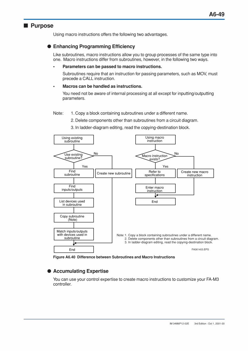
A6-49
IM 34M6P12-02E 3rd Edition : Oct 1, 2001-00
PurposeUsing macro instructions offers the following two advantages.
Enhancing Programming Efficiency
Like subroutines, macro instructions allow you to group processes of the same type intoone. Macro instructions differ from subroutines, however, in the following two ways.
• Parameters can be passed to macro instructions.
Subroutines require that an instruction for passing parameters, such as MOV, mustprecede a CALL instruction.
• Macros can be handled as instructions.
You need not be aware of internal processing at all except for inputting/outputtingparameters.
Note: 1. Copy a block containing subroutines under a different name.
2. Delete components other than subroutines from a circuit diagram.
3. In ladder-diagram editing, read the copying-destination block.
Using existingsubroutine
Use existing subroutine?
Findsubroutine
Findinputs/outputs
List devices usedin subroutine
Copy subroutine (Note)
Match inputs/outputswith devices used in
subroutine
End
Create new subroutine Create new macroinstruction
Using macroinstruction
Macro instructionexists?
Refer tospecifications
Enter macroinstruction
End
No
Yes
No
Yes
FA061403.EPS
Note: 1. Copy a block containing subroutines under a different name. 2. Delete components other than subroutines from a circuit diagram. 3. In ladder-diagram editing, read the copying-destination block.
Figure A6.40 Difference between Subroutines and Macro Instructions
Accumulating Expertise
You can use your control expertise to create macro instructions to customize your FA-M3controller.

A6-50
IM 34M6P12-02E 3rd Edition : Oct 1, 2001-00
A6.13.2 Specification of Macro Instructions
Supported CPU ModulesMacro instructions are only supported for the F3SP25 and F3SP35 sequence CPU mod-ules.
Number of Macro InstructionsCalled-side macro instructions are downloaded, along with user ladder diagrams, from apersonal computer to the CPU module using the programming tool*. You can include amaximum of 64 called-side macro instructions in one executable program during download-ing. In addition, you can use each calling-side macro instruction in your user ladderprogram any number of times.
* WideField or Ladder Diagram Support Program M3
Size of Macro-instruction ProgramThe size of a program of called-side macro instructions is limited by the total size of thatprogram and user programs combined.
Macro Instruction Execution Time
Table A6.14 Macro Instruction Execution Time
FUNCNo.
TA061401.EPS
F3SP25Mnemonic When not
executed(esec)
Whenexecuted(esec)
When notexecuted(esec)
Whenexecuted(esec)
F3SP35Instruction
996
995
998
Macro instruction call
Parameter instruction
Macro instruction return
MCALL
PARA
MRET
22.0
8.0
10.0
0.6
0.36
—
16.5
6.0
7.5
0.45
0.27
—
Online Macro Instruction EditingYou can use the online edit function of the programming tool for user-created ladder dia-grams containing calling-side macro instructions. In that case however, you can only usemacro instructions that have already been downloaded. You cannot create a new macroinstruction. You can also edit online called-side macro instructions which have alreadybeen downloaded. It is not possible, however, to edit online any circuit diagram that followsan MRET macro return instruction.
Making Macro Instructions Resident in ROMLike programs, you can make macro instructions resident in a ROM pack. This is automati-cally done when you transfer a program to the ROM pack using the ROM writer function ofthe CPU module.

A6-51
IM 34M6P12-02E 3rd Edition : Oct 1, 2001-00
A6.13.3 Devices Dedicated to Macro InstructionsTable A6.15 lists devices dedicated to macro instructions.
Table A6.15 Devices Dedicated to Macro Instructions
Device
TA061402.EPS
QuantityRangeCode
P
H
A
U
16
512
512
16
Pointer register
Macro relay
Macro register
Macro index register
P01 to P16
H0001 to H0512
A0001 to A0512
U01 to U16
F3SP25, F3SP35
Pointer (P) RegistersPointer registers are dedicated to macro instructions and used to pass parameters tomacro instructions. You can use these registers for called-side macro instructions. TableA6.16 shows the relationship between pointer registers and macro instruction operands.
FA061404.EPS
MY00301I0001D0001EFG123
Operand3Operand2Operand1
Table A6.16 Relationship between Pointer Registers and Macro Instruction Operands
Operand No. Pointer Register No.
1
2
3
4
16
P01
P02
P03
P04
P16
Parameters that can be directly passed using a macroinstruction call
Parameters that can be passed using a parameterinstruction
T061303.EPS
Using a basic or advanced instruction, you can read from and write to pointer registers in amacro instruction just like devices passed as parameters. You can also apply a word/longword process, index modification process, and automatic BIN-to-BCD or BCD-to-BINconversion process to these pointer registers. High speed processing of advanced instruc-tions is not performed, however. More specifically, high speed processing does not apply toa MOV, CAL, CMP, or logical operation instruction that uses pointer registers in a macroinstruction as its operands.
TIP
When executing two or more instructions that use pointer registers, it is recommended thatyou first transfer the values of the pointer registers to macro relays/registers. Then, executetwo or more instructions that use these macro relays/registers. This strategy reduces theinstruction execution time.

A6-52
IM 34M6P12-02E 3rd Edition : Oct 1, 2001-00
X00502V011MOV
M
R00014PARA
Y00301
V01
I0001D0001EFG123
M033A00011MOV
U012MOV
A0001U01
+P01=P04
A0001U01
+D0001=R0002
MRET
Real "EFG123" macro instruction (called side)
Pointer register specified in a macro instruction (called side)
(Note)
(Note) Pointer registers can be used for real macro instructions (called side).
FA061406.EPS
P04=R0002
P01=D0001P02=I0001P03=Y00301(Nemonic: MCALL EFG123 D0001 I0001 Y00301)
Figure A6.41 Example of Using Pointer Registers
CAUTION
• If you pass a device accompanied by an index modification device to a macro instruc-tion as a parameter, the instruction receives an already index-modified device. In theexample of Figure A6.41, the parameter R0001;V01 equals the device R0002 be-cause V01 = 1.
• Any index modification in a pointer register applies to a parameter that is passed. Inthe example of Figure A6.41, the parameter P01;U01 equals the device D0003because P01 = D0001 and U01 = 2.
Macro Relays (H), Macro Registers (A) and Macro Index Registers (U)These devices are dedicated to macro instructions. Using a basic or advanced instruction,you can read from and write to a macro relay, macro register and macro index register in acalled-side macro instruction just like an internal relay (I), data register (D) and indexregister (V). These devices can be used for called-side macro instructions.
You can use these devices in your macro instruction without having to be aware whichdevices are used in the instruction when applying the instruction. Needless to say, thevalues of these devices are retained.

A6-53
IM 34M6P12-02E 3rd Edition : Oct 1, 2001-00
A6.13.4 Nesting Macro InstructionsNesting macro instructions enables you to call another macro instruction when executingthe current execution. If you nest macro instruction calls to a depth of more than eightlevels, an instruction processing error will result. The depth of nesting is stored in specialregister Z106. The value “0” is stored in the special register Z106 if you execute any non-nested macro instruction.
CAUTION
Parameters 1 to 3 to be passed to macro instructions are saved when the macro instruc-tions are nested. However, parameters 4 to 16 passed by parameter instructions are notsaved. If a parameter instruction is executed in a called macro instruction, the relevantparameters are overwritten.
SEE ALSO
Subsection 3.13.6, “Macro Instructions, Parameter Instructions, Macro Instruction Returns”in the 2nd or later edition of, Sequence CPU Instruction Manual - Instructions (IM34M6P12-03E), for details on parameter instructions.

A6-54
IM 34M6P12-02E 3rd Edition : Oct 1, 2001-00
When nesting macro instructions, you may mistakenly overwrite macro devices, such asrelays, registers and index registers, in a called macro instruction and thereby destroy theirdata. To avoid this problem, check the depth of macro instruction nesting stored in specialregister Z106 and use macro devices separately for each level of nesting depth (see theexample below).
X00501D0002D0001NEST1
X00502
U01P2A01NEST2
1+P1=A01
64*Z106=U01
0 0
64Z106=U01
MRET
X00503
U01P2A01NEST3
1+P1=A01
64Z106=U01
U01
64Z106=U01
MRET
Real NEST 1 macro instruction
Real NEST 2 macro instruction
A01 (A001 to A064 can be used.)
The NEST 2 instruction damages U01.
64 0
A01 (A001 to A064 can be used.)
The NEST 3 instruction damages U01.
*
*
*
FA061407.EPS
M
M
Figure A6.42 Example of Using Macro Devices Separately when Nesting Macro Instructions

A6-55
IM 34M6P12-02E 3rd Edition : Oct 1, 2001-00
A6.13.5 Handling Macro Instruction ErrorsAn error occurs when creating a program using a macro instruction tool if:
• there are two or more macro instructions of the same name,
• a macro instruction specified in an MCALL macro instruction call is not found, or
• any single macro instruction contains two or more MRET macro return instructions.
An error also occurs and the special relay M201 for instruction processing errors is set toON if:
• an MRET ladder macro instruction return is executed before an MCALL macroinstruction call (special register Z022 contains the error code $2501), or
• the depth of macro instruction call nesting exceeds eight levels (special register Z022contains the error code $2502).
An error encountered in a called-side macro instruction is viewed by the user as an error ina calling-side macro instruction. Thus, the user can know which parameters were passedto the macro instruction.
CAUTION
An error, except a check-sum memory error, found by self-diagnosis in a called-side macroinstruction is also viewed by the user as an error that has occurred as the result of execut-ing a calling-side macro instruction.
It is not possible to determine in which downloaded-type macro instruction a check-summemory error is found. Therefore, the error is recognized when it is detected, rather thanwhen the macro instruction is executed.
Table A6.17 Error Codes for Macro Instructions
Error Type
TA061403.EPS
DescriptionError CodeError Name
$2501
Instruction processing Macro instruction error
There is no return destination.
The upper limit of nesting depth, i.e., eight levels, has been exceeded.$2502
A6-56
IM 34M6P12-02E 3rd Edition : Oct 1, 2001-00
A6.13.6 Protecting Macro InstructionsYou can protect macro instructions from being referenced by someone else to ensure thesecurity of called-side macro instructions. This protection is achieved for each macroinstruction by entering a password with the WideField or Ladder Diagram Support ProgramM3. A password must consist of eight alphanumeric characters, beginning with a letter.The protection information is saved in the management information area of a macro in-struction file. You are not allowed to perform macro instruction editing, printing and monitor-ing for macro instructions under protection unless your password matches.
CAUTION
Executable program protection and block protection are effective for user-created ladderprograms that contain macro instructions. If, for example, executable program protection isenabled, any act of working with executable programs, such as downloading, uploading,monitoring or online-editing, becomes impracticable.
A6.13.7 Debugging Operation
Forced-Set/ResetYou can also turn on and off bit devices forcibly in calling-side and called-side macroinstructions.
Step and Partial OperationsPartial operation is not possible with calling-side and called-side macro instructions.
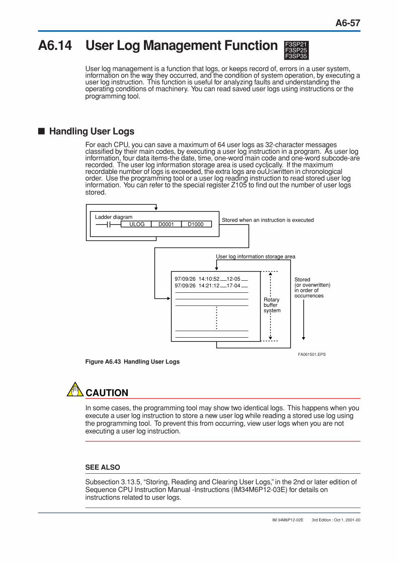
A6-57
IM 34M6P12-02E 3rd Edition : Oct 1, 2001-00
A6.14 User Log Management Function F3SP35F3SP25F3SP21
User log management is a function that logs, or keeps record of, errors in a user system,information on the way they occurred, and the condition of system operation, by executing auser log instruction. This function is useful for analyzing faults and understanding theoperating conditions of machinery. You can read saved user logs using instructions or theprogramming tool.
Handling User LogsFor each CPU, you can save a maximum of 64 user logs as 32-character messagesclassified by their main codes, by executing a user log instruction in a program. As user loginformation, four data items-the date, time, one-word main code and one-word subcode-arerecorded. The user log information storage area is used cyclically. If the maximumrecordable number of logs is exceeded, the extra logs are ouÚ≤written in chronologicalorder. Use the programming tool or a user log reading instruction to read stored user loginformation. You can refer to the special register Z105 to find out the number of user logsstored.
Ladder diagramD1000D0001ULOG
97/09/26 14:10:5297/09/26 14:21:12
12-0517-04
Stored when an instruction is executed
User log information storage area
Rotarybuffersystem
Stored (or overwritten) in order ofoccurrences
FA061501.EPS
Figure A6.43 Handling User Logs
CAUTION
In some cases, the programming tool may show two identical logs. This happens when youexecute a user log instruction to store a new user log while reading a stored use log usingthe programming tool. To prevent this from occurring, view user logs when you are notexecuting a user log instruction.
SEE ALSO
Subsection 3.13.5, “Storing, Reading and Clearing User Logs,” in the 2nd or later edition ofSequence CPU Instruction Manual -Instructions (IM34M6P12-03E) for details oninstructions related to user logs.

Blank Page

A7-1
IM 34M6P12-02E 3rd Edition : Oct 1, 2001-00
A7. I/O Response Time Based on Scan TimeThis chapter discusses examples of calculating the scan time and I/O response time.It also explains such parameters as instruction execution time.
A7.1 Scan TimeAs discussed earlier in Chapter A3, the sequence CPU module is designed so that twosystems of processes, i.e., a system of control-related processes and a system ofperipheral processes, run concurrently and independently. For this reason, the system ofcontrol-related processes whose main purpose is to execute programs and control-relatedprocesses is not affected by the system of peripheral processes whose purpose is tosupport communication and programming tools. Thus, the system of control-relatedprocesses can run at extremely high speeds. Under normal conditions, the scan time of thesequence CPU module is equivalent to the time taken by the system of control-relatedprocesses. The following paragraphs explain the processing tasks and time of each ofthese systems.
System of Control-related Processes
The latest, maximum and minimum scan times taken by the system of control-relatedprocesses are stored in special registers Z001 to Z003 in that order.
Table A7.1 Scan Time of System of Control-related Processes
TA070101.EPS
Item Processing Task Processing Time
Common processing Self-diagnosis Fixed at 0.5 ms.
Program execution Executes ladder programs. The scan time is calculated using the program execution time or output refreshing time, whichever is greater.
The scan time is the sum of the execution times of basic and advanced instructions. It varies depending on the type of CPU module and the execution time of each instruction word. See Section A7.5, "Instruction Execution Time," for more information.
Output refreshing Writes the contents of Y output relays to an output module.
12 µs 3 number of modules calculated on a 16-device basis*
Input refreshing Reads the contents of 3 input relays to write them to the output module.
6 µs 3 number of modules calculated on a 16-device basis*
Synchronization processing Ensures synchronization and the simul-taneity of data for operation- and con-trol-related processes between the sys-tem of control-related processes and the system of peripheral processes.
• When output relays are used:8 µs3number of modules calculated on a 16-device basis*
• When FA link modules are used:0.003 3 (number of relays used in FA link for refreshing/16 ( number of registers used in FA link for refreshing) +0.05 ms.
• When an add-on CPU is installed:0.002 3 (number of relays set in local CPU/32 • number of registers set in local CPU/2)+0.05 ms.

A7-2
IM 34M6P12-02E 3rd Edition : Oct 1, 2001-00
* Relationship between Types of I/O Module and Number of Modules Calculated on a16-device Basis
TA070102.EPS
Type of I/O Module Number of Modules Calculated on a 16-device Basis
4-point I/O relay
8-point I/O relay
14-point I/O relay
16-point I/O relay
32-point I/O relay
64-point I/O relay
1
1
1
1
2
4
System of Peripheral Processes
The latest, maximum and minimum scan times taken by the system of peripheralprocesses are stored in special registers Z007 to Z009 in that order.
Table A7.2 Scan Time of System of Peripheral Processes
T070103.EPS
Item Processing Task Processing Time
Link refreshing Updates the contents of link relays and registers when an FA link module is installed.
When an FA link module is installed:0.015 T (number of relays used in FA link for refreshing/16 + number of registers used in FA link for refreshing) + 0.06 ms
Not performed if no FA link module is installed.
When no FA link module is installed: 0.00 ms
Shared refreshing Updates the contents of shared/extended shared relays and shared/extended shared registers when an add-on CPU is installed.In a single refreshing cycle, this task updates the contents of shared/extended shared relays or shared/extended shared registers included in the configuration setting, for each CPU.
When an add-on CPU is installed:0.014 T (number of relays set in CPU for refreshing/32 + number of registers set in CPU for refreshing/2) + 0.10 ms
Not performed if no add-on CPU is installed.
When no add-on CPU is installed: 0.00 ms
Tool service Processes commands input from a programming tool connected to the CPU. Executes one command per service.
Varies with the type command.
Link service Processes commands input from a personal computer link module. Executes one command per service.
Varies with the type command.
CPU service Processes commands input from a remote CPU module. Executes one command per service.
Varies with the type command.
A7.2 Setting Scan Time Monitoring TimeThis configuration item sets the scan time monitoring time. You can set the time within therange of 10 ms to 200 ms, in 10 ms increments. By default, the time is set at 200 ms.
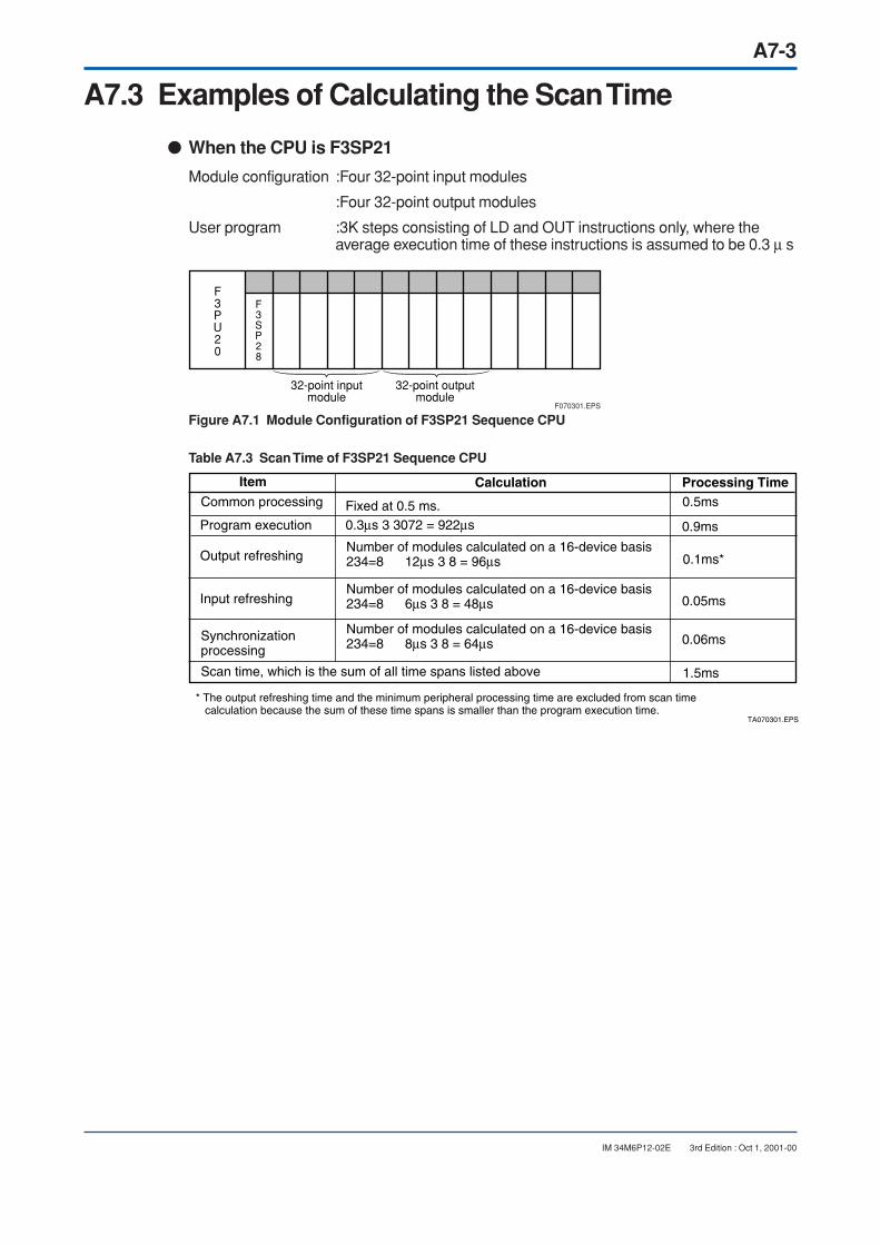
A7-3
IM 34M6P12-02E 3rd Edition : Oct 1, 2001-00
A7.3 Examples of Calculating the Scan Time
When the CPU is F3SP21
Module configuration :Four 32-point input modules
:Four 32-point output modules
User program :3K steps consisting of LD and OUT instructions only, where theaverage execution time of these instructions is assumed to be 0.3 µ s
32-point inputmodule
32-point outputmodule
F3PU20
F3SP28
F070301.EPS
Figure A7.1 Module Configuration of F3SP21 Sequence CPU
Table A7.3 Scan Time of F3SP21 Sequence CPU
TA070301.EPS
Item Calculation Processing TimeCommon processing Fixed at 0.5 ms. 0.5ms
Program execution
Number of modules calculated on a 16-device basis234=8 12µs 3 8 = 96µs
Number of modules calculated on a 16-device basis234=8 6µs 3 8 = 48µs
Number of modules calculated on a 16-device basis234=8 8µs 3 8 = 64µs
Output refreshing
Input refreshing
Synchronizationprocessing
Scan time, which is the sum of all time spans listed above
* The output refreshing time and the minimum peripheral processing time are excluded from scan time calculation because the sum of these time spans is smaller than the program execution time.
0.3µs 3 3072 = 922µs 0.9ms
0.1ms*
0.05ms
0.06ms
1.5ms

A7-4
IM 34M6P12-02E 3rd Edition : Oct 1, 2001-00
When the CPU Is F3SP35
Module configuration: Four 32-point input modules
:Four 32-point output modules
User program :5K steps consisting of LD and OUT instructions only, where theaverage execution time of these instructions is assumed to be 0.15 µ s
32-point inputmodule
32-point outputmodule
F3PU20
F3SP58
F070302.EPS
Figure A7.2 Module Configuration of F3SP35 Sequence CPU
Table A7.4 Scan Time of F3SP35 Sequence CPU
T070302.EPS
Item Calculation Processing TimeCommon processing Fixed at 0.5 ms. 0.5ms
Program executionNumber of modules calculated on a 16-points basis12µs T 8 = 96µs
Output refreshing
Input refreshing Number of modules calculated on a 16-points basis2 T 4 = 8 6µs T 8 = 48µs
Synchronizationprocessing
Number of modules calculated on a 16-points basis2 T 4 = 8 6µs T 8 = 48µs
* The output refreshing time and the minimum peripheral processing time are excluded from scan time calculation because the sum of these time spans is smaller than the program execution time. calculation because the sum of these time spans is smaller than the program execution time.
0.15µs T 3072 = 717µs 0.5ms
0.1ms*
0.05ms
0.06ms
0.1msScan time, which is the sum of all time spans listed above

A7-5
IM 34M6P12-02E 3rd Edition : Oct 1, 2001-00
A7.4 Examples of Calculating the I/O Response Time
Calculation of the minimum I/O response time
Input response time :16 ms
Output response time :1 ms
Scan time :2 ms
Minimum I/O response time = Input response time + Scan time + Output response time
= 16 ms + 2 ms + 1 ms = 19 ms
X00502 Y00602
Input refreshing
Instruction execution Instruction execution
Input
Output
X00502
Y00602
Output refreshing
One scan
F070401.EPS
Figure A7.3 Minimum I/O Response Time
Calculation of the maximum I/O response time
Input response time :16 ms
Output response time :1 ms
Scan time :2 ms
Maximum I/O response time = Input response time + (Scan time T 2) + Output responce time
= 16 ms + (2 T 2) ms + 1 ms = 21 ms
X00502 Y00602
Input refreshing
Instruction execution Instruction execution
Input
Output
X00502
Y00602
Output refreshing
One scanOne scan
F070402.EPS
Figure A7.4 Maximum I/O Response Time
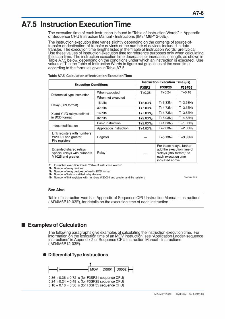
A7-6
IM 34M6P12-02E 3rd Edition : Oct 1, 2001-00
A7.5 Instruction Execution TimeThe execution time of each instruction is found in “Table of Instruction Words” in Appendixof Sequence CPU Instruction Manual - Instructions (IM34M6P12-03E).The instruction execution time varies slightly depending on the contents of source-of-transfer or destination-of-transfer devices or the number of devices included in datatransfer. The execution time lengths listed in the “Table of Instruction Words” are typical.Use these values of instruction execution time for reference purposes only when calculatingthe scan time. The instruction execution time decreases or increases in length, as shown inTable A7.5 below, depending on the conditions under which an instruction is executed. Usevalues of T in the Table of Instruction Words to figure out guidelines of the scan timeaccording to the formulas given in Table A7.5.
Table A7.5 Calculation of Instruction Execution Time
TA070501.EPS
Execution ConditionsInstruction Execution Time (µs)
F3SP21 F3SP25 F3SP35
T+0.36
T+5.03N1
T+7.03N1
T+7.03N2
T+9.03N2
T+2.03N3
T+4.03N4
—
—
T+0.24
T+3.33N1
T+4.73N1
T+4.73N2
T+6.03N2
T+1.33N3
T+2.63N4
T+5.13N4
T+0.18
T+2.53N1
T+3.53N1
T+3.53N2
T+4.53N2
T+1.03N3
T+2.03N4
T+3.83N4
When executed
When not executed
16 bits
32 bits
16 bits
32 bits
Basic instruction
Application instruction
Register
Relay
Differential type instruction
Relay (BIN format)
X and Y I/O relays definedin BCD format
Index modification
T: Instruction execution time in "Table of Instruction Words"N1: Number of relay devicesN2: Number of relay devices defined in BCD formatN3: Number of index-modified relay devicesN4: Number of link registars with numbers W20001 and greater and file resisters
Link registers with numbers W20001 and greater File registers
Extended shared relaysSpecial relays with numbers M1025 and greater
For these relays, further add the execution time of "relays (BIN format)" to each execution time indicated above.
See Also
Table of instruction words in Appendix of Sequence CPU Instruction Manual - Instructions(IM34M6P12-03E), for details on the execution time of each instruction.
Examples of CalculationThe following paragraphs give examples of calculating the instruction execution time. Forinformation on the execution time of an MOV instruction, see “Application Ladder-sequenceInstructions” in Appendix 2 of Sequence CPU Instruction Manual - Instructions(IM34M6P12-03E).
Differential Type Instructions
MOV D0001 D0002
0.36 + 0.36 = 0.72 s (for F3SP21 sequence CPU) 0.24 + 0.24 = 0.48 s (for F3SP25 sequence CPU)0.18 + 0.18 = 0.36 s (for F3SP35 sequence CPU)
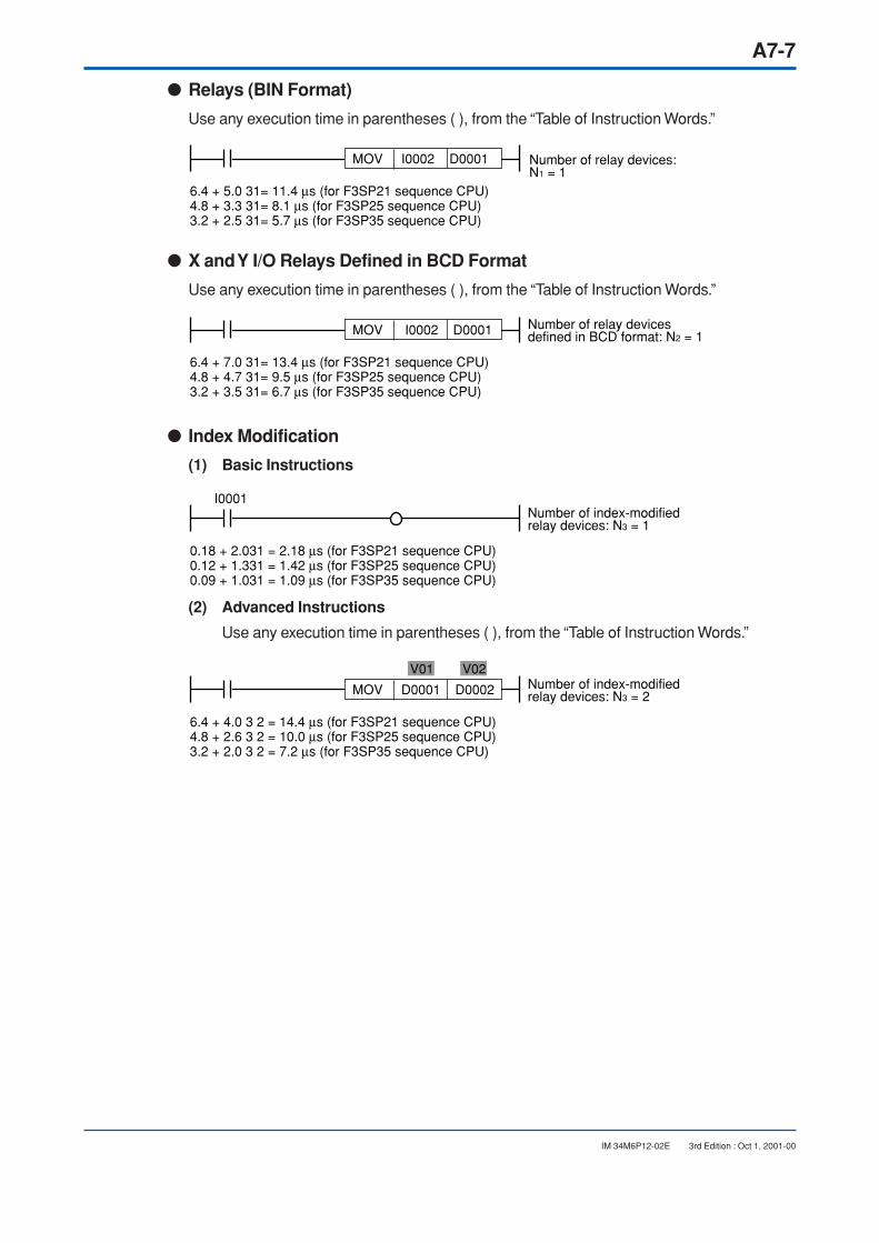
A7-7
IM 34M6P12-02E 3rd Edition : Oct 1, 2001-00
Relays (BIN Format)
Use any execution time in parentheses ( ), from the “Table of Instruction Words.”
MOV I0002 D0001
6.4 + 5.0 31= 11.4 µs (for F3SP21 sequence CPU)4.8 + 3.3 31= 8.1 µs (for F3SP25 sequence CPU) 3.2 + 2.5 31= 5.7 µs (for F3SP35 sequence CPU)
Number of relay devices:N1 = 1
X and Y I/O Relays Defined in BCD Format
Use any execution time in parentheses ( ), from the “Table of Instruction Words.”
MOV I0002 D0001
6.4 + 7.0 31= 13.4 µs (for F3SP21 sequence CPU) 4.8 + 4.7 31= 9.5 µs (for F3SP25 sequence CPU)3.2 + 3.5 31= 6.7 µs (for F3SP35 sequence CPU)
Number of relay devicesdefined in BCD format: N2 = 1
Index Modification
(1) Basic Instructions
0.18 + 2.031 = 2.18 µs (for F3SP21 sequence CPU) 0.12 + 1.331 = 1.42 µs (for F3SP25 sequence CPU)0.09 + 1.031 = 1.09 µs (for F3SP35 sequence CPU)
Number of index-modifiedrelay devices: N3 = 1
I0001
(2) Advanced Instructions
Use any execution time in parentheses ( ), from the “Table of Instruction Words.”
MOV D0001 D0002
6.4 + 4.0 3 2 = 14.4 µs (for F3SP21 sequence CPU) 4.8 + 2.6 3 2 = 10.0 µs (for F3SP25 sequence CPU)3.2 + 2.0 3 2 = 7.2 µs (for F3SP35 sequence CPU)
Number of index-modifiedrelay devices: N3 = 2
V01 V02
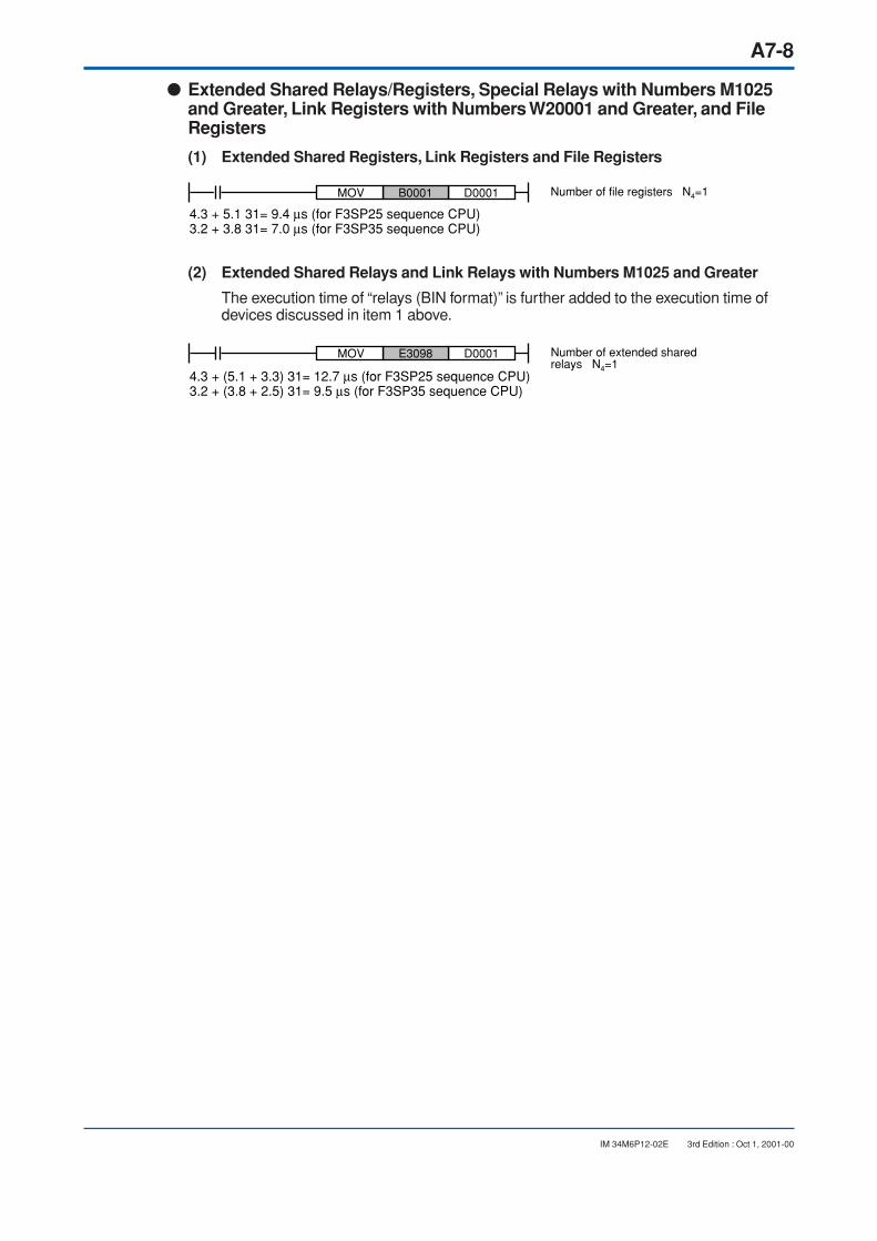
A7-8
IM 34M6P12-02E 3rd Edition : Oct 1, 2001-00
Extended Shared Relays/Registers, Special Relays with Numbers M1025and Greater, Link Registers with Numbers W20001 and Greater, and FileRegisters
(1) Extended Shared Registers, Link Registers and File Registers
B0001 D0001MOV
4.3 + 5.1 31= 9.4 µs (for F3SP25 sequence CPU) 3.2 + 3.8 31= 7.0 µs (for F3SP35 sequence CPU)
Number of file registers N4=1
(2) Extended Shared Relays and Link Relays with Numbers M1025 and Greater
The execution time of “relays (BIN format)” is further added to the execution time ofdevices discussed in item 1 above.
E3098 D0001MOV
4.3 + (5.1 + 3.3) 31= 12.7 µs (for F3SP25 sequence CPU) 3.2 + (3.8 + 2.5) 31= 9.5 µs (for F3SP35 sequence CPU)
Number of extended sharedrelays N4=1
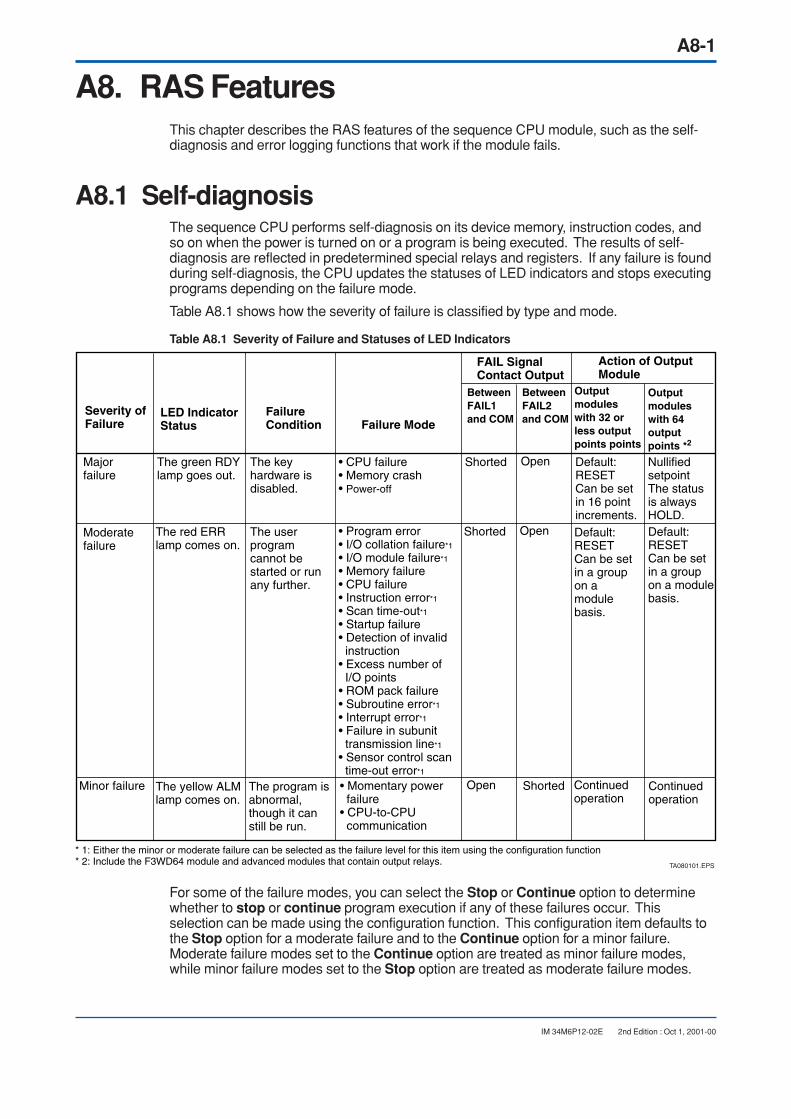
A8-1
IM 34M6P12-02E 2nd Edition : Oct 1, 2001-00
A8. RAS FeaturesThis chapter describes the RAS features of the sequence CPU module, such as the self-diagnosis and error logging functions that work if the module fails.
A8.1 Self-diagnosisThe sequence CPU performs self-diagnosis on its device memory, instruction codes, andso on when the power is turned on or a program is being executed. The results of self-diagnosis are reflected in predetermined special relays and registers. If any failure is foundduring self-diagnosis, the CPU updates the statuses of LED indicators and stops executingprograms depending on the failure mode.
Table A8.1 shows how the severity of failure is classified by type and mode.
Table A8.1 Severity of Failure and Statuses of LED Indicators
TA080101.EPS
Severity ofFailure
LED Indicator Status
FailureCondition Failure Mode
FAIL SignalContact Output
BetweenFAIL1and COM
BetweenFAIL2and COM
Action of Output Module
Output modules with 64 output points *2
Output modules with 32 or less output points points
Major failure
The green RDY lamp goes out.
The key hardware is disabled.
• CPU failure• Memory crash• Power-off
Shorted Open Default: RESETCan be set in 16 point increments.
Nullified setpointThe status is always HOLD.
Moderate failure
The red ERR lamp comes on.
The user program cannot be started or run any further.
• Program error• I/O collation failure*1
• I/O module failure*1
• Memory failure• CPU failure• Instruction error*1
• Scan time-out*1• Startup failure• Detection of invalid instruction• Excess number of I/O points• ROM pack failure• Subroutine error*1
• Interrupt error*1
• Failure in subunit transmission line*1
• Sensor control scan time-out error*1
Shorted Open Default: RESETCan be set in a group on a module basis.
Default: RESETCan be set in a group on a module basis.
Minor failure The yellow ALM lamp comes on.
The program is abnormal, though it can still be run.
• Momentary power failure• CPU-to-CPU communication
Open Shorted Continued operation
Continued operation
* 1: Either the minor or moderate failure can be selected as the failure level for this item using the configuration function* 2: Include the F3WD64 module and advanced modules that contain output relays.
For some of the failure modes, you can select the Stop or Continue option to determinewhether to stop or continue program execution if any of these failures occur. Thisselection can be made using the configuration function. This configuration item defaults tothe Stop option for a moderate failure and to the Continue option for a minor failure.Moderate failure modes set to the Continue option are treated as minor failure modes,while minor failure modes set to the Stop option are treated as moderate failure modes.

A8-2
IM 34M6P12-02E 3rd Edition : Oct 1, 2001-00
CAUTION
• If you want the contacts of an output module to be reset in case of a major ormoderate failure in the sequence CPU module, use an output module with 32 or lessoutput points and set the “Output in case of CPU stop” option of the configurationfunction to RESET.
• If you want the contacts of an output module to be held in case of a major or moderatefailure in the sequence CPU module, set the “Output in case of CPU stop” option ofthe configuration function to HOLD. Note that there is no difference in the moduleaction due to a difference in the type of output module.

A8-3
IM 34M6P12-02E 2nd Edition : Oct 1, 2001-00
Table A8.2 Details on Self-diagnosis (1 of 6)
TA080201.EPS
Failure Mode
SpecialRelaythatTurnson
SpecialRegistersthat StoreErrorCodes, Etc.
StoredErrorCode Failure Description Corrective Actions
1.Check the installation environment for possible problems, such as noise sources. If the failure recurs, replace the module.
1.It is likely that restrictions on module installation have been violated. Check the modules according to Section 1.2, "Restrictions on Installing Modules," in the instruction manual Sequence CPUs Hardware.2.Check the installation environment for possible problems, such as noise sources. If the failure recurs, replace the module.
1.Check the installation environment for possible problems, such as noise sources. If the failure recurs, replace the module.
1.It is likely that the error is due to a transient memory failure caused by effects of noise. Check the installation environment. Clear the memory by referring to CAUTION at the end of tables and download the program once again. If the failure recurs, replace the module.
1.Check if there is any error in the values of index registers or in the parameters defining the number of devices in an instruction for globally rewriting multiple devices, such as a BMOV block transfer instruction.
1.It is likely that the error is due to a transient memory failure caused by effects of noise. Check the installation environment. Clear the memory by referring to CAUTION at the end of tables and download the program once again. If the failure recurs, replace the module.
Major failure
CPU failure - - -
The CPU malfunctions due to noise or for other reasons.Hardware failure
Hardware failure
Moderate failure
Startup failure
M193 Z017 to Z019
$10nn A failure has occurred during CPU initialization.
$11nnSPUfailure
The CPU for sequence computing has failed.
$1201
$1202
Memory failure
A program checksum error has occurred.
Transient memory failure or hardware failure (See CAUTION at the end of tables for information on how to discriminate between these failures).
Inadvertent writing has been done to the M129 to M131 special relays for handling Run, Debug and Stop mode flags.
Application
Hardware failure
A device memory read/write check error has occurred.
A system memory read/write check error has occurred.
An invalid instruction has been encountered.
There is no END instruction in the program.
$1203
$1701
$1702
Detection of invalid instruction

A8-4
IM 34M6P12-02E 3rd Edition : Oct 1, 2001-00
Table A8.2 Details on Self-diagnosis (2 of 6)
TA080202.EPS
Failure Mode
SpecialRelaythatTurnson
SpecialRegistersthat StoreErrorCodes, Etc.
StoredErrorCode Failure Description Corrective Actions
1.Verify compatibility among the JMP, SUB and RET instructions.2.It is likely that the error is due to a transient memory failure caused by effects of noise. Check the installation environment. Clear the memory as instructed in CAUTION at the end of section and download the program again. If the failure recurs, replace the module.
The JMP, SUB and RET instructions are not compatible with one another.
Wrong input to programmable controllerHardware failure
Moderate failure
M193 Z017 to Z019
Program error
$2001
Excess number of I/O points
$2002 The number of I/O points has been exceeded.
1.It is likely that restrictions on module installation have been violated. Check the modules according to Section 1.2, "Restrictions on Installing Modules," in the instruction manual Sequence CPUs-Hardware.
ROM pack failure
$8203 The ROM pack is incompatible with the CPU.
Mismatch between ROM pack and CPU Hardware failure
1.A ROM pack whose data has been erased is in no way defective. Use it as is.2.It is likely that data has been written to the ROM pack under a wrong CPU name. Rewrite to the ROM pack and try using it again. The ROM pack or CPU module may be defective if the same failure recurs. Replace the ROM pack or CPU module.
$8204 It is not possible to read from or write to the ROM pack.
Hardware failure 1.Rewrite to the ROM pack and try using it again. The ROM pack or CPU module may be defective if the same failure recurs. Replace the ROM pack or CPU module.
Battery failure
M194 - $1801 The backup batteries have failed.
1.The power supply module may be defective if the same failure recurs. Replace the module.
Sub-routine error(Note)
M201 Z022 to Z024
$2201 The RET instruction has not been executed because there is no return destination.
Application error 1.Check if there is such an error as a jump out of or into the subroutine 2.Check if a scan timeout has been detected within the subroutine.
$2202 The maximum nesting depth of eight levels has been exceeded.
1.Check the depth of nesting when calling another subroutine in a given subroutine.
Note: For this failure mode, you can determine whether to stop or continue program execution.
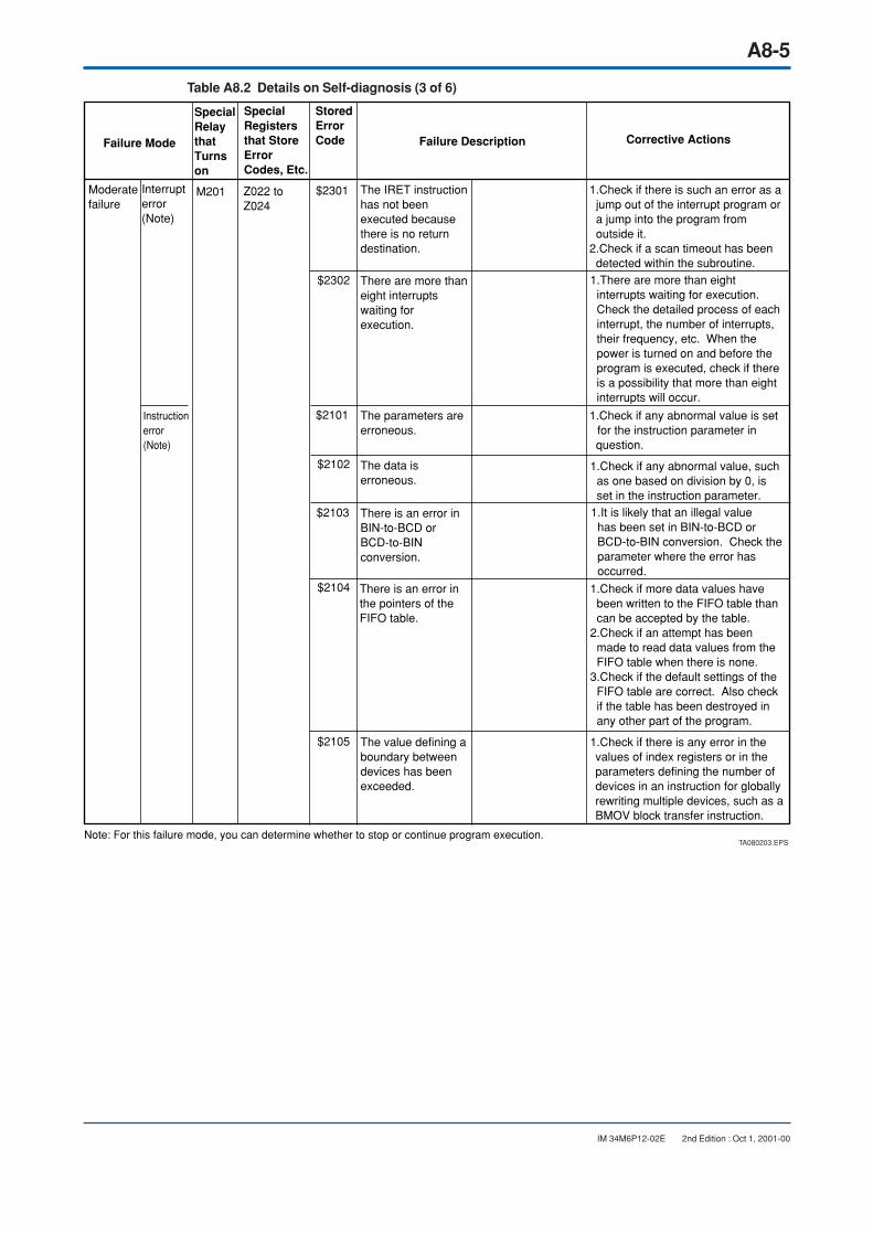
A8-5
IM 34M6P12-02E 2nd Edition : Oct 1, 2001-00
Table A8.2 Details on Self-diagnosis (3 of 6)
TA080203.EPS
Failure Mode
SpecialRelaythatTurnson
SpecialRegistersthat StoreErrorCodes, Etc.
StoredErrorCode Failure Description Corrective Actions
Moderate failure
M201 Z022 to Z024
$2301Interrupt error(Note)
1.Check if there is such an error as a jump out of the interrupt program or a jump into the program from outside it.2.Check if a scan timeout has been detected within the subroutine.
The IRET instruction has not been executed because there is no return destination.
$2302 There are more than eight interrupts waiting for execution.
1.There are more than eight interrupts waiting for execution. Check the detailed process of each interrupt, the number of interrupts, their frequency, etc. When the power is turned on and before the program is executed, check if there is a possibility that more than eight interrupts will occur.
Note: For this failure mode, you can determine whether to stop or continue program execution.
Instruction error(Note)
$2101 The parameters are erroneous.
1.Check if any abnormal value is set for the instruction parameter in
question.
$2102 The data is erroneous.
1.Check if any abnormal value, such as one based on division by 0, is set in the instruction parameter.
$2103 There is an error in BIN-to-BCD or BCD-to-BIN conversion.
1.It is likely that an illegal value has been set in BIN-to-BCD or BCD-to-BIN conversion. Check the parameter where the error has occurred.
$2104 There is an error in the pointers of the FIFO table.
1.Check if more data values have been written to the FIFO table than can be accepted by the table.2.Check if an attempt has been made to read data values from the FIFO table when there is none.3.Check if the default settings of the FIFO table are correct. Also check if the table has been destroyed in any other part of the program.
1.Check if there is any error in the values of index registers or in the parameters defining the number of devices in an instruction for globally rewriting multiple devices, such as a BMOV block transfer instruction.
The value defining a boundary between devices has been exceeded.
$2105

A8-6
IM 34M6P12-02E 3rd Edition : Oct 1, 2001-00
Table A8.2 Details on Self-diagnosis (4 of 6)
TA080204.EPS
Failure Mode
SpecialRelaythatTurnson
SpecialRegistersthat StoreErrorCodes, Etc.
StoredErrorCode Failure Description Corrective Actions
Moderate failure
M201 Z022 to Z024
Note: For this failure mode, you can determine whether to stop or continue program execution.
Instruction error(Note1)
$2106 The FOR-NEXT loop is not consistent.
1.Check if there is such an error as a jump out of or into the FOR-NEXT loop.
2.Check if a scan timeout has been detected within the FOR-NEXT loop.
I/O collation failure(Note)
M202 Z027 to Z029
$2401 ¥ The condition of module installation is not consistent with the program.¥ The number of HRD/HWR instructions has exceeded the limit (error code:$2401).
Application failure 1.It is likely that there is a mismatch between the X and Y I/O relay devices specified in the program and those contained in the installed I/O module. Check if the instruction parameter in question is consistent with the installed I/O module.2.Check if the number of each of the HRD and HWR instructions has exceeded 64.
$2402(READ/WRITE)
$2402(READ/WRITE)
1.It is likely that there is a mismatch between the slot number in HRD/HWR instructions used in the program and that of the installed I/O module. Check if the instruction parameter in question is consistent with the installed I/O module.
$2403(READ/WRITE)
$2403(READ/WRITE)
1.It is likely that there is a mismatch between the slot number in READ/WRITE instructions used in the program and that of the installed I/O module. Check if the instruction parameter in question is consistent with the installed I/O module.
I/O failure(Note)
M203 Z033 to Z040
- ¥ It is not possible to read from or write to the I/O module.¥ There is a communication failure in the fiber- optic FA-bus module.¥ An attempt has been made to reset a remote CPU in a multi-CPU system.
1.Check if the subunit is turned off.2.Check if there is any problem with the cable of the fiber-optic FA-bus module.3.Do not reset the CPUs individually. Reset them all at once from the main CPU.
4.The I/O module may be defective. Replace it.

A8-7
IM 34M6P12-02E 2nd Edition : Oct 1, 2001-00
Table A8.2 Details on Self-diagnosis (5 of 6)
TA080205.EPS
Failure Mode
SpecialRelaythatTurnson
SpecialRegistersthat StoreErrorCodes, Etc.
StoredErrorCode Failure Description Corrective Actions
Moderate failure
M204
Note: For this failure mode, you can determine whether to stop or continue program execution.
- -Scan timeout(Note)
The scan time monitoring time has been exceeded.
Application failure 1.Check if the repetition-counter values of the FOR-NEXT loop are correct.2.Check if the FOR-NEXT loop has been mistakenly turned into an endless loop by JMP instructions.3.Adjust the scan time monitoring time according to the execution time of the application program.
M210Failure in subunit transmission line(Note)
Z089 to Z096
- It is not possible to read from or write to the subunit.
Open-circuited cable Loss of power to subunit Hardware failure
1.Check if the subunit is turned off.2.Check if there is any problem with the cable of the fiber-optic FA-bus module.3.The fiber-optic FA-bus module may be defective. Replace it.
Minor failure
Momentary power failure
The CPU indicates that a momentary power failure has occurred.
M195 - - 1.If this failure mode occurs too frequently, check the power supply for possible problems. If a UPS is in use, check that it has captured peak values of its supply voltage waveform. If the failure still occurs frequently while there is no problem with the waveform, it is likely that the power supply module and/or CPU module is defective. Replace
it.
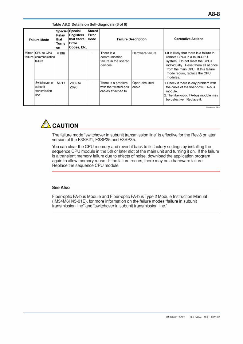
A8-8
IM 34M6P12-02E 3rd Edition : Oct 1, 2001-00
Table A8.2 Details on Self-diagnosis (6 of 6)
TA080206.EPS
Failure Mode
SpecialRelaythatTurnson
SpecialRegistersthat StoreErrorCodes, Etc.
StoredErrorCode Failure Description Corrective Actions
Minor failure
M196 - -CPU-to-CPU communication failure
There is a communication failure in the shared devices.
Hardware failure 1.It is likely that there is a failure in remote CPUs in a multi-CPU system. Do not reset the CPUs individually. Reset them all at once
from the main CPU. If this failure mode recurs, replace the CPU modules.
M211Switchover in subunit transmission line
Z089 to Z096
- There is a problem with the twisted-pair cables attached to
Open-circuited cable
1.Check if there is any problem with the cable of the fiber-optic FA-bus module.2.The fiber-optic FA-bus module may be defective. Replace it.
CAUTION
The failure mode “switchover in subunit transmission line” is effective for the Rev.8 or laterversion of the F3SP21, F3SP25 and F3SP35.
You can clear the CPU memory and revert it back to its factory settings by installing thesequence CPU module in the 5th or later slot of the main unit and turning it on. If the failureis a transient memory failure due to effects of noise, download the application programagain to allow memory reuse. If the failure recurs, there may be a hardware failure.Replace the sequence CPU module.
See Also
Fiber-optic FA-bus Module and Fiber-optic FA-bus Type 2 Module Instruction Manual(IM34M6H45-01E), for more information on the failure modes “failure in subunittransmission line” and “switchover in subunit transmission line.”

A8-9
IM 34M6P12-02E 2nd Edition : Oct 1, 2001-00
A8.1.1 Setting Operation Mode in Case of Failure and ExternalOutput Mode in Case of Sequence Stop
Setting Operation Mode in Case of FailureUsing the configuration function, determine whether to stop (for moderate failures) orcontinue (for minor failures) executing sequence programs in case of such a fault as aninstruction processing failure. The table below summarizes the configuration items andtheir defaults. If a failure for which you have selected the Continue option actually occurs,the CPU fails to correctly perform such tasks as accessing the I/O module that caused thefailure or processing instructions.
Configuration Item Default
I/O module failure
I/O collation failure
Instruction processing error
Scan time-out
Subroutine error
Interrupt error
Failure in subunit transmission line
Stop (for moderate failures)
TA080104.EPS
Continue (for minor failures)
CAUTION
Use the R1.08 or later version of Ladder Diagram Support Program M3 to edit theconfiguration item “Failure in Subunit Transmission Line.” This item is effective for the Rev.8or later version of the F3SP21, F3SP25 and F3SP35 sequence CPU modules.
See Also
Fiber-optic FA-bus Module and Fiber-optic FA-bus Type 2 Module Instruction Manual(IM34M6H45-01E), for more information on the failure modes “failure in subunittransmission line” and “switchover in subunit transmission line.”
A8-10
IM 34M6P12-02E 3rd Edition : Oct 1, 2001-00
A8.2 Recovering Normal Operation after CorrectingModerate/Minor Failures
After eliminating the cause of a moderate or minor failure, initialize the states of specialrelays, special registers and LED indicators as instructed below.
Recovery after Correcting Moderate FailuresAfter correcting any moderate failure, reset the special relays and special registers and turnoff the ERR indicator lamp by:
• turning on the power again, and
• setting the sequence CPU in the Run or Debug mode using the programming tool.
Recovery after Correcting Minor FailuresAfter correcting any minor failure, reset the special relays and special registers and turn offthe ALM indicator lamp by:
• turning on the power again,
• setting the sequence CPU in the Run or Debug mode using the programming tool,and
• performing an “alarm acknowledgement.”
Toc-B1
IM 34M6P12-02E
CONTENTS
3rd Edition : Oct 1, 2001-00
IM 34M6P12-02E 3rd Edition
Sequence CPU Instruction Manual - FunctionsPART B for CPU module designed for theFA-M3 Value system (F3SP05-0P)
B1. Specification and Basic Configuration ................................................ B1-1B1.1 Overview........................................................................................................ B1-1
B1.2 Specification ................................................................................................. B1-3
B1.2.1 Performance Data ........................................................................... B1-3
B1.2.2 Device List ...................................................................................... B1-5
B1.2.3 Configuration .................................................................................. B1-6
B1.2.4 Components and Their Functions ................................................... B1-8
B1.2.5 External Dimensions ....................................................................... B1-9
B1.3 Basic Configuration .................................................................................... B1-10
B1.3.1 Units ............................................................................................. B1-10
B1.3.2 Slot Number ................................................................................. B1-11
B1.3.3 I/O Relay Number ......................................................................... B1-11
B2. System Configuration .......................................................................... B2-1B2.1 Basic System Configuration ........................................................................ B2-1
B2.2 Extended System Configuration .................................................................. B2-2
B2.2.1 Remote I/O System ........................................................................ B2-2
B2.2.2 Personal Computer Link System ..................................................... B2-3
B2.2.3 FA Link System ............................................................................... B2-3
B2.3 Programming Tools ....................................................................................... B2-4
B2.3.1 WideField ....................................................................................... B2-4
B2.3.2 Ladder Diagram Support Program M3 ............................................ B2-6

Blank Page

B1-1
IM 34M6P12-02E 3rd Edition : Oct 1, 2001-00
B1. Specification and Basic ConfigurationThis chapter explains the specification of the F3SP05-0P sequence CPU moduledesigned for the FA-M3 Value system (Model F3SC21-1N Controller) and thesystem’s basic configuration.
B1.1 Overview
OverviewModel F3SP05-0P is a sequence CPU module with a built-in power supply and memoryand is used to configure the FA-M3 Value system. The built-in power supply is functionallyequivalent to the F3PU10-0N power supply module. The sequence CPU is alsofunctionally equivalent to the F3SP21-0N except for the CPU’s 5K-step program size. Thischapter focuses on the CPU of the F3SP05-0P module. For details on the power supplyblock of the module, refer to the part “FA-M3 Value (Model F3SC21-1N)” of HardwareManual (IM34M6C11-01E).
For further details on instructions available with the F3SP05-0P module, refer to theF3SP21’s Sequence CPU Instruction Manual - Instructions (IM34M6P12-03E), as suchspecifications as device sizes and instructions available with the F3SP05-0P are the sameas those of the F3SP21 sequence CPU module.
CAUTION
The R2.02 or a later version of Ladder Diagram Support Program M3 is required to use theF3SP05-0P sequence CPU module.
Features• Has a compact body, allowing for space saving within the cabinet.
• Support for high-speed processes and responses of the module’s maximuminstruction processing speed.
• Operates large-capacity programs and has large device sizes, enabling it to cope withadvanced, complex control applications.
• Uses index modification and structured ladder language for easy program design andmaintenance.
• Allows the device size and operating method to be flexibly configured according toyour application needs.
• Provides various functions, e.g., a forced SET/RESET function and scan operationindependent of program computation results, for easy program debugging andmaintenance.
• Has a carefully designed self-diagnosis function, in addition to a highly reliable design.
• Can connect to a host computer or a monitor without the need for a personal computerlink module, as the programming tool connection port supports a personal computerlink function.
B1-2
IM 34M6P12-02E 3rd Edition : Oct 1, 2001-00
• Has a logging function capable of recording errors encountered in a program, as wellas messages created and registered in advance.
• Allows you to attach a ROM pack so that you can perform ROM-based operation andstore programs.
• Has a program protection function to ensure security.
Major Functions• Configuration (setup of parameters, including device size, range of devices to be
latched in case of power failure, and external output to be retained in case ofsequence stop)
• Constant scan (at an interval of 1 to 190 ms, in 0.1 ms increments)
• Debugging (forced SET/RESET instructions, online editing, scan operation, etc.)
• Error logging, user logging
• Clock (year, month, day, hour, minute, second, and day of the week)
• Support for programming tool connection port with the personal computer link function
• Program protection
• Program/data storage in ROM pack
* See Section B1.2, “Specification,” for more information.

B1-3
IM 34M6P12-02E 3rd Edition : Oct 1, 2001-00
B1.2 Specification
B1.2.1 Performance DataTable B1.1 Performance Data (1 of 2)
Control method
I/O computation method
Programming language
Number of I/O points
Number of internal relays (I)
Number of shared relays (E)
Number of extended shared relays (E)
Number of link relays (L)
Number of special relays (M)
Number of timers (T)
Number of counters (C)
Number of data registers (D)
Number of shared registers (R)
Number of extended shared registers (R)
Number of file registers (B)
Number of link registers (W)
Number of special registers (Z)
Number of labels
Number of interruption processing routines
Decimal constant
Hexadecimal constant
Character-string constant
Floating-point constant
Repetitive computation based on stored programs
Refreshing by direct I/O instructions
Structured ladder language and mnemonic language
2048 max.
4096
0
0
2048
2048
256
256
5120
0
0
0
2048
256
64
4
16-bit instruction: -32768 to 3276732-bit instruction: -2147483648 to 2147473647
16-bit instruction: $0 to $FFFF (hexadecimal number)32-bit instruction: $0 to $FFFFFFFF (hexadecimal number)
16-bit instruction: "AB", "YOKO", etc.32-bit instruction: "ABCD", "YOKOGAWA", etc.
32-bit instruction: "1.23", "-3.21", etc.Approximately -3.4 3 1038 to 3.4 3 1038
Item Specifications
Constants
TB010201.EPS
*
* The inputs of F3WD32-3F cannot be used as interrupt inputs.
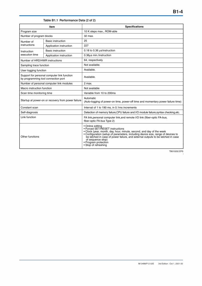
B1-4
IM 34M6P12-02E 3rd Edition : Oct 1, 2001-00
Table B1.1 Performance Data (2 of 2)
Number of personal computer link modules
Macro instruction function
Scan time monitoring time
Startup at power-on or recovery from power failure
Constant scan
Self-diagnosis
Link function
Other functions
2 max.
Not available
Variable from 10 to 200ms
Interval of 1 to 190 ms, in 0.1ms increments
Detection of memory failure,CPU failure and I/O module failure,syntax checking,etc.
Automatic(Auto-logging of power-on time, power-off time and momentary power failure time)
• Online editing• Forced SET/RESET instructions• Clock (year, month, day, hour, minute, second, and day of the week• Configuration (setup of parameters, including device size, range of devices to be latched in case of power failure, and external outputs to be latched in case of sequence stop)• Program protection• Stop of refreshing
FA link,personal computer link,and remote I/O link (fiber-optic FA-bus,fiber-optic FA-bus Type 2)
Program size
Number of program blocks
Basic instruction
Application instruction
Basic instruction
Application instruction
Number of HRD/HWR instructions
Sampling trace function
User logging function
Support for personal computer link function by programming tool connection port
Number of instructions
Instructionexecution time
10 K steps max., ROM-able
32 max.
25
227
0.18 to 0.36 µs/instruction
0.36µs min./instruction
64, respectively
Not available.
Available.
Available.
Item Specifications
TB010202.EPS
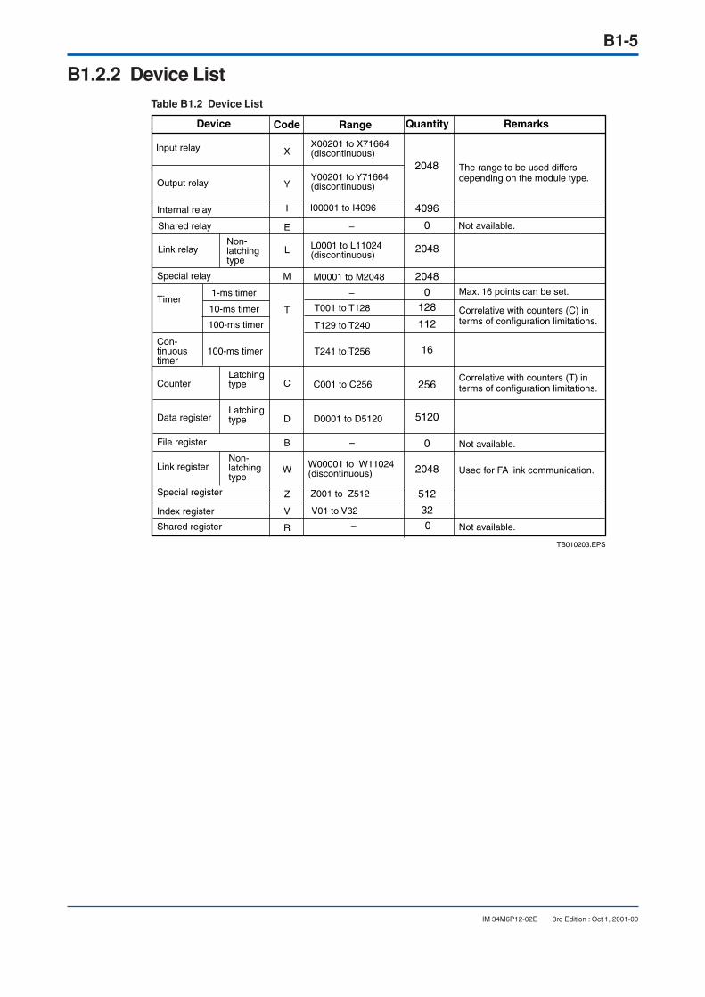
B1-5
IM 34M6P12-02E 3rd Edition : Oct 1, 2001-00
B1.2.2 Device ListTable B1.2 Device List
Input relay X00201 to X71664 (discontinuous)
Y00201 to Y71664 (discontinuous)Output relay
Internal relay
Shared relay
Link relay
Special relay
Timer
Con-tinuous timer
Counter
Data register
File register
Link register
Special register
Index register
Shared register
I00001 to I4096
L0001 to L11024(discontinuous)
M0001 to M2048
–
–
T001 to T128
T129 to T240
T241 to T256
C001 to C256
–
–
D0001 to D5120
W00001 to W11024(discontinuous)
Z001 to Z512
V01 to V32
The range to be used differs depending on the module type.
Correlative with counters (C) in terms of configuration limitations.
Correlative with counters (T) in terms of configuration limitations.
Non-latching type
1-ms timer
10-ms timer
100-ms timer
100-ms timer
Latching type
Latching type
Non-latching type
Device Code Range Quantity Remarks
X
Y
I
E
L
M
T
C
D
B
W
Z
V
R
2048
4096
0
2048
2048
5120
256
16
112
1280
0
2048
512
32
0
TB010203.EPS
Not available.
Not available.
Not available.
Max. 16 points can be set.
Used for FA link communication.

B1-6
IM 34M6P12-02E 3rd Edition : Oct 1, 2001-00
B1.2.3 Configuration
Configuration FunctionThe sequence CPU contains the predefined defaults of device sizes and operation meth-ods.
You can run programs with these defaults. In some applications, however, they may not suityour specific purpose. In such a case, flexibility allows for defaults to be changed to meetyour needs. Changing the defaults is called "configuration" and can be performed througha programming tool.
Table B1.3 Configuration Ranges (1 of 2)
Item
TB010204.EPS
Default
Internal relay (I) 4096
0
256
256
5120
0
0
128
112
16
Link register (W)
Link register (W)
Configuration Range
Shared relays (E)
Counter (C)
Data register (D)
Shared registers (R)
Link relay (L)
Link relay (L)
Timer (T)
Internal relay (I)
Counter (C)
Data register (D)
Timer (T)
Devicesize
Timer
1-ms timer
10-ms timer
100-ms timer
100-ms continuous timer
Rangeof linkrelays/registers
Range of link data Link relays (L)/registers (W)
Configurable in 16 points increments for each link module (2 modules max.)Configurable in 32 points increments; continuous from the starting numberConfigurable in 16 points increments; continuous from the starting numberConfigurable in 1 point increments; continuous from the starting numberConfigurable in 1 point increments; continuous from the starting number
Configurable in 2 points increments; continuous from the starting number
Range of devices to be latched in case of power failure
–
–
–
512 units in 1 point increments for timers and counters com-
Configurable in16 points incre-ments for each link
Configurable in 1 point incre-ments for each link
Configurable in 1 point incre-ments;16 units max. for 1-ms timers;
32 units for each station
32 units for each station
Non-latching type
I0001 to I1024
Non-latching type
Non-latching type(except for continuous timers)
All latched (C001 to C256)
All latched (D0001 to D5120)

B1-7
IM 34M6P12-02E 3rd Edition : Oct 1, 2001-00
Item
TB010205.EPS
Default Configuration Range
Data register (D)Configurable for up to 1024 points continuously from the starting number
Configurable from 10 to 200 ms in 10 ms increments
Configurable from 1.0 to 190.0 ms in 0.1 ms increments
Selectable from Stop and Continue options.
Selectable from Retained/Not Retained options on a module basis
Initial data
Ope-ration mode in case of failure
I/O module
Devices' current values to be made resident in ROM
Momentary power failure detection mode Standard mode
None
None
200 msScan time monitoring time
Constant scan time Normal scan
I/O module failure
I/O collation failure
Instruction processing failure
Scan timeout
Subroutine error
Interrupt error
Subunit transmission line failure
Stop
Stop
Stop
Stop
Stop
Stop
Continuation
Output mode in case of sequence stop OFF
BIN
16 ms
BIN/BCD; configurable in 16 points increments
16 ms/1 ms; configurable in 16 points increments
Configurable for up to 5120 points continuously from the starting number
Standard mode
Data code type
Input sampling interval
Data and file registers
Program execution mode All blocks All blocks/Specified blocks
ModeMode 0: 9600 bps, even parityMode 1: 9600 bps, non parityMode 2: 19200 bps, even parity
Related/Not relatedBetween each FA link number and slots 1 to 16
Relationship between FA link numbers and slot numbers
CPU commu-nication port
Personal computer link func-tion
Mode 0: 9600 bps,even parity
Used/unused
Check sum
Terminal character selection
Protection function
Unused
None
None
None
None
Unused/Used
Yes/No
Yes/No
Yes/No
Note: For more information on configuration when FA link H and/or fiber-optic FA link H modules are used, see Section A4.3, "Link Relays and Link Registers," of Chapter A4, "Devices," in the main part of this instruction manual and FA Link H Module F3LP02-0N Fiber-optic FA Link H Modules F3LP12-0N (IM34M6H43-01E).
Table B1.3 Configuration Ranges (2 of 2)
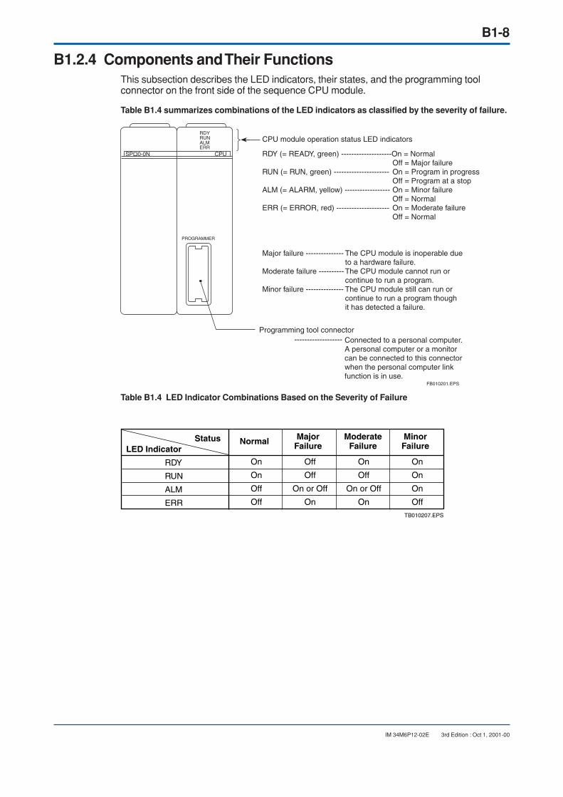
B1-8
IM 34M6P12-02E 3rd Edition : Oct 1, 2001-00
B1.2.4 Components and Their FunctionsThis subsection describes the LED indicators, their states, and the programming toolconnector on the front side of the sequence CPU module.
Table B1.4 summarizes combinations of the LED indicators as classified by the severity of failure.
FB010201.EPS
SP0-0N CPU
CPU module operation status LED indicators
RDY (= READY, green) --------------------On = Normal Off = Major failureRUN (= RUN, green) ---------------------- On = Program in progress Off = Program at a stopALM (= ALARM, yellow) ------------------ On = Minor failure Off = NormalERR (= ERROR, red) --------------------- On = Moderate failure Off = Normal
Major failure --------------- The CPU module is inoperable due to a hardware failure.
Moderate failure ---------- The CPU module cannot run or continue to run a program.
Minor failure --------------- The CPU module still can run or continue to run a program though it has detected a failure.
Programming tool connector ------------------- Connected to a personal computer.
A personal computer or a monitor can be connected to this connector when the personal computer link function is in use.
Table B1.4 LED Indicator Combinations Based on the Severity of Failure
Status Normal
On Off On On
On Off Off On
Off On or Off On or Off On
Off On On Off
MajorFailure
ModerateFailure
MinorFailureLED Indicator
RDY
RUN
ALM
ERRTB010207.EPS
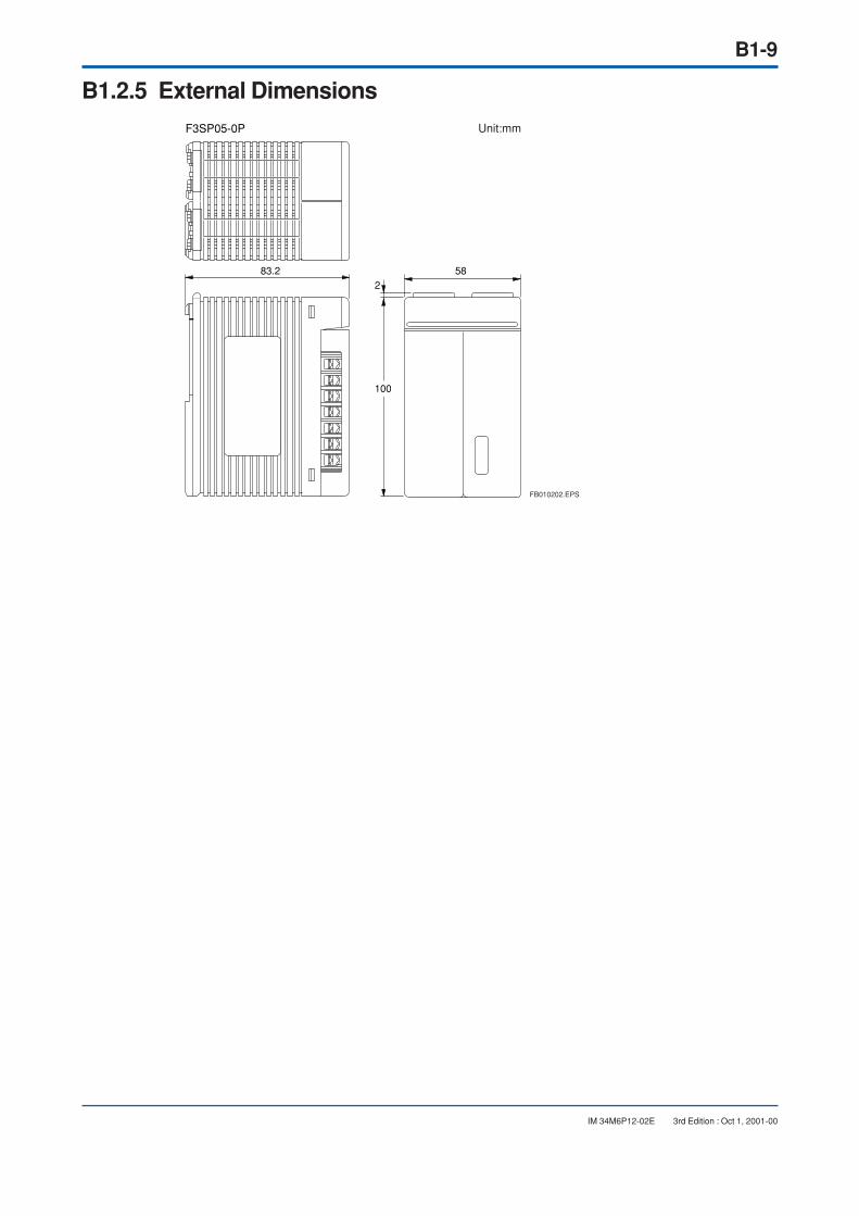
B1-9
IM 34M6P12-02E 3rd Edition : Oct 1, 2001-00
B1.2.5 External Dimensions
83.2 582
100
F3SP05-0P
FB010202.EPS
Unit:mm

B1-10
IM 34M6P12-02E 3rd Edition : Oct 1, 2001-00
B1.3 Basic Configuration
B1.3.1 Units
Main UnitIn the case of the FA-M3 Value system, the F3SC21-1N controller is called a main unit andconsists of the following modules.
• F3BU04-0N base module
• F3SP05-0P sequence CPU module with power supply and memory
• F3WD64-3N I/O module
Install the F3SP05-0P sequence CPU module in the leftmost slot of the F3BU04-0N basemodule and the F3WD64-3N I/O module in slot 2. In the remaining third and fourth slots,install other necessary I/O modules or special modules.
SubunitA unit that contains no CPU modules and is connected to the main unit through a fiber-opticFA-bus or fiber-optic FA-bus type 2 is called a subunit. The subunit consists of the moduleslisted in Table B1.5. A maximum of seven subunits can be connected to the main unit andare identified by their unit numbers.
Table B1.5 Subunit Components
Name Description
Base module Five types are available depending on the number of modules to be mounted.
One power supply module must always be mounted on the base module.
Various types are available, including analog I/O and communication modules.
Power supply module
CPU module
I/O module
Special moduleTB010301.EPS
At least one CPU module is required. Several types are available depending on the functionality.
Various types are available depending on the type of I/O and the number of I/O points.

B1-11
IM 34M6P12-02E 3rd Edition : Oct 1, 2001-00
B1.3.2 Slot NumberA slot number indicates the position of a slot where a module is installed. The slot numberis defined as a three-digit integer, as shown below.
FB010301.EPS
Slot number
Slot positions 01 to 16 are assigned to the slot on the immediate right of the power supply module through to the rightmost slot of a base module.
Unit numberMain unit = 0Subunit = 1 to 7
Figure B1.1 Slot Numbers
B1.3.3 I/O Relay NumberEach input relay (X) and output relay (Y) number is defined as a slot number followed by aterminal number. The terminal number is a number corresponding to each terminal of an I/O module.
Example) The output relay number for terminal 6 of an F3YC08-0N module installedin slot 004 is defined as follows.
FB010302.EPS
Y
001 002 003 004
Y004 06Terminal numberSlot number
Slot numbers
Output relay number Y00406
OUT08-
F3YC08-0N
Figure B1.2 I/O Relay Number
The input and output terminal numbers of a mixed-I/O module or multifunctional modulewith 32 input and output points each are assigned as 1 to 32 and as 33 to 64, respectively.

Blank Page

B2-1
IM 34M6P12-02E 3rd Edition : Oct 1, 2001-00
B2. System ConfigurationThis chapter describes the configuration of a small-scale control system and pro-gramming tools.
B2.1 Basic System ConfigurationThe basic system configuration only refers to a system consisting of a main unit. For moreinformation on the main unit, see subsection B1.3.1, "Units."
FB020101.EPS
Sequence CPU module or BASIC CPU module
Figure B2.1 Example of Basic System Configuration

B2-2
IM 34M6P12-02E 3rd Edition : Oct 1, 2001-00
B2.2 Extended System ConfigurationThe extended system configuration refers to a system configured by adding remote I/Omodules, a personal computer link module, and an FA link module to the basic system.
B2.2.1 Remote I/O SystemThe remote I/O system refers to a system configured using fiber-optic FA-bus or FA-bustype 2 communication modules.
The number of remote I/O points is included in the count of all I/O points.
FB020202.EPS
Main unit
Subunit
Subunit
Fiber-optic FA-bus type 2 module
Fiber-optic cable
Fiber-optic FA-bus type 2 module
Fiber-optic cable
Figure B2.2 Example of System Using Fiber-optic FA-bus Type 2 Modules

B2-3
IM 34M6P12-02E 3rd Edition : Oct 1, 2001-00
B2.2.2 Personal Computer Link SystemThe personal computer link system refers to a system configured by connecting a personalcomputer or a monitor to the main unit through a personal computer link module. Thesequence CPU module can be connected directly to a personal computer or a monitorthrough the module's programming port.
FB020203.EPS
Personal computer or monitor with PC interface
Main unit
Personal computer link module
Figure B2.3 Example of Personal Computer Link System
B2.2.3 FA Link SystemThe FA link system refers to a system that employs FA link communication to build a net-work system with programmable controllers.
The combinations of the types of communication and associated modules covered by anFA link system are:
FA link H communication and FA link H module
Fiber-optic FA link H communication and fiber-optic FA link H module
Unless otherwise specified, "FA link" in this manual is a general term for these two types ofcommunication. For more information on the FA link, see FA Link H Module F3LP02-0NFiber-optic FA Link H Module F3LP12-0N (IM34M6H43-01E).
FB020204.EPS
Main unit Main unit
FA link
Main unit
FA link H module, Fiber-optic FA link H module
Figure B2.4 Example of FA Link System

B2-4
IM 34M6P12-02E 3rd Edition : Oct 1, 2001-00
B2.3 Programming ToolsThe FA-M3 Programming Tool WideField and Ladder Diagram Support Program M3 areavailable as programming tools for the F3SP05-0P sequence CPU module.
B2.3.1 WideFieldThe table below presents an overview of WideField.
Description Software Model Supported CPUs
FA-M3 Programming Tool WideField SF610-JCW
TB020301.EPS
F3SP05 F3SP38F3SP21 F3SP53F3SP25 F3SP58F3SP28 F3FP36F3SP35
FB020301.EPS
Personal computer
Sequence CPU module
Figure B2.5 Overview of WideField
Object LadderWideField defines "blocks" and "macros" that compose a ladder program as "objects," aterm commonly used in the computing world. The object-oriented ladder languageassumes responsibility for a given function and features a high degree of independence.Consequently, the language offers higher productivity and better maintainability than astructured programming language. It is therefore effective for the reuse of ladder programs.
Features
Treatment as Components
Blocks can be reused as sheer components. Devices that are used only within a block aredefined separately. WideField eliminates the chance of using the same device twice andmakes it easy to recombine blocks.
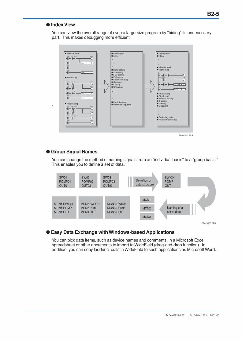
B2-5
IM 34M6P12-02E 3rd Edition : Oct 1, 2001-00
Index View
You can view the overall range of even a large-size program by "hiding" its unnecessarypart. This makes debugging more efficient
.
FB020302.EPS
I*****
I*****
I*****
I*****
Y*****
Y*****
Y*****
Y*****
I*****
I*****
I*****
I*****
I*****
I*****
I*****
I*****
I*****
Y*****
Y*****
I*****
I*****
I*****
I*****
I*****
I*****
I*****
I*****
I***** Y*****I***** I*****
CAL =
MOVE
+
I*****
I*****
I*****
I*****
Y*****
Y*****
I*****
I*****
I*****
I*****
I*****
CAL =
MOVE
+
CAL =
MOVE
+
Material feed Initialization Idling
Fault-diagnosis Power-off sequence
Material feed Preheating Flux coating Finish coat Fixation heating Cleaning Cooling Unloading
Preheating
Flux coating
•
•
•
•
•
•
Initialization Idling
Fault-diagnosis Power-off sequence
Material feed Preheating
•••
•••
Flux coating Finish coat Fixation heating Cleaning Cooling Unloading
Group Signal Names
You can change the method of naming signals from an "individual basis" to a "group basis."This enables you to define a set of data.
SW01POMP01OUT01
MCN1.SWICHMCN1.POMPMCN1.OUT
MCN2.SWICHMCN2.POMPMCN3.OUT
MCN3.SWICHMCN3.POMPMCN3.OUT
SW02POMP02OUT02
SW03POMP03OUT03
SWICHPOMPOUT
Definition of data structure
Naming of a set of data
MCN1
MCN2
MCN3
FB020303.EPS
Easy Data Exchange with Windows-based Applications
You can pick data items, such as device names and comments, in a Microsoft Excelspreadsheet or other documents to import to WideField (drag-and-drop function). Inaddition, you can copy ladder circuits in WideField to such applications as Microsoft Word.
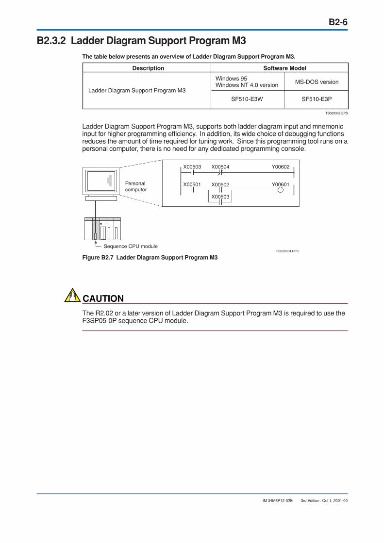
B2-6
IM 34M6P12-02E 3rd Edition : Oct 1, 2001-00
B2.3.2 Ladder Diagram Support Program M3The table below presents an overview of Ladder Diagram Support Program M3.
Description Software Model
Ladder Diagram Support Program M3
Windows 95Windows NT 4.0 version
TB020302.EPS
MS-DOS version
SF510-E3W SF510-E3P
Ladder Diagram Support Program M3, supports both ladder diagram input and mnemonicinput for higher programming efficiency. In addition, its wide choice of debugging functionsreduces the amount of time required for tuning work. Since this programming tool runs on apersonal computer, there is no need for any dedicated programming console.
FB020304.EPS
Personalcomputer
X00503 X00504
X00501 X00502
X00503
Y00602
Y00601
Sequence CPU module
Figure B2.7 Ladder Diagram Support Program M3
CAUTION
The R2.02 or a later version of Ladder Diagram Support Program M3 is required to use theF3SP05-0P sequence CPU module.
Toc-C1
IM 34M6P12-02E
CONTENTS
3rd Edition : Oct 1, 2001-00
IM 34M6P12-02E 3rd Edition
Sequence CPU Instruction Manual - FunctionsPART C for CPU module designed for theFA-M3 Value II system (F3SP08-0P)
C1. Specification and Basic Configuration ................................................ C1-1C1.1 Overview........................................................................................................ C1-1
C1.2 Specification ................................................................................................. C1-3
C1.2.1 Performance Data ........................................................................... C1-3
C1.2.2 Device List ...................................................................................... C1-5
C1.2.3 Configuration .................................................................................. C1-6
C1.2.4 Components and Their Functions ................................................... C1-8
C1.2.5 External Dimensions ....................................................................... C1-9
C1.3 Basic Configuration .................................................................................... C1-10
C1.3.1 Units ............................................................................................. C1-10
C1.3.2 Slot Number ................................................................................. C1-11
C1.3.3 I/O Relay Number ......................................................................... C1-11
C2. System Configuration .......................................................................... C2-1C2.1 Basic System Configuration ........................................................................ C2-1
C2.2 Extended System Configuration .................................................................. C2-2
C2.2.1 Remote I/O System ........................................................................ C2-2
C2.2.2 Personal Computer Link System ..................................................... C2-3
C2.2.3 FA Link System ............................................................................... C2-3
C2.3 Programming Tools ....................................................................................... C2-4
C2.3.1 WideField ....................................................................................... C2-4

Blank Page
C1-1
IM 34M6P12-02E 3rd Edition : Oct 1, 2001-00
C1. Specification and Basic ConfigurationThis chapter explains the specification of the F3SP08-0P sequence CPU moduledesigned for the FA-M3 Value system (Model F3SC22- Controller) and thesystem’s basic configuration.
C1.1 Overview
OverviewModel F3SP08-0P is a sequence CPU module with a built-in power supply and memoryand is used to configure the FA-M3 Value II system. The built-in power supply is function-ally equivalent to the F3PU10-0N power supply module. The sequence CPU is also func-tionally equivalent to the F3SP21-0N. This chapter focuses on the CPU of the F3SP08-0Pmodule. For details on the power supply block of the module, refer to the part “FA-M3 ValueII (Model F3SC22-)” of Hardware Manual (IM34M6C11-01E).
For further details on instructions available with the F3SP08-0P module, refer to theF3SP21’s Sequence CPU Instruction Manual - Instructions (IM34M6P12-03E), as suchspecifications as device sizes and instructions available with the F3SP08-0P are the sameas those of the F3SP21 sequence CPU module.
CAUTION
The R2.06 or a later version of FA-M3 Programming Tool WideField is required to use theF3SP08-0P sequence CPU module.
Features• Has a compact body, allowing for space saving within the cabinet.
• Support for high-speed processes and responses of the module’s maximum instruc-tion processing speed.
• Operates large-capacity programs and has large device sizes, enabling it to cope withadvanced, complex control applications.
• Uses index modification and structured ladder language for easy program design andmaintenance.
• Allows the device size and operating method to be flexibly configured according toyour application needs.
• Provides various functions, e.g., a forced SET/RESET function independent ofprogram computation results, for easy program debugging and maintenance.
• Has a carefully designed self-diagnosis function, in addition to a highly reliable design.
• Can connect to a host computer or a monitor without the need for a personal computerlink module, as the programming tool connection port supports a personal computerlink function.
C1-2
IM 34M6P12-02E 3rd Edition : Oct 1, 2001-00
• Has a logging function capable of recording errors encountered in a program, as wellas messages created and registered in advance.
• Allows you to attach a ROM pack so that you can perform ROM-based operation andstore programs.
• Has a program protection function to ensure security.
Major Functions• Configuration (setup of parameters, including device size, range of devices to be
latched in case of power failure, and external output to be retained in case of se-quence stop)
• Constant scan (at an interval of 1 to 190 ms, in 0.1 ms increments)
• Debugging (forced SET/RESET instructions, online editing, etc.)
• Error logging, user logging
• Clock (year, month, day, hour, minute, second, and day of the week)
• Support for programming tool connection port with the personal computer link function
• Program protection
• Program/data storage in ROM pack
* See Section C1.2, “Specification,” for more information.

C1-3
IM 34M6P12-02E 3rd Edition : Oct 1, 2001-00
C1.2 Specification
C1.2.1 Performance DataTable C1.1 Performance Data (1 of 2)
Control method
I/O computation method
Programming language
Number of I/O points
Number of internal relays (I)
Number of shared relays (E)
Number of extended shared relays (E)
Number of link relays (L)
Number of special relays (M)
Number of timers (T)
Number of counters (C)
Number of data registers (D)
Number of shared registers (R)
Number of extended shared registers (R)
Number of file registers (B)
Number of link registers (W)
Number of special registers (Z)
Number of labels
Number of interruption processing routines
Decimal constant
Hexadecimal constant
Character-string constant
Floating-point constant
Repetitive computation based on stored programs
Refreshing by direct I/O instructions
Structured ladder language and mnemonic language
2048 max.
4096
0
0
2048
2048
256
256
5120
0
0
0
2048
256
64
4
16-bit instruction: -32768 to 3276732-bit instruction: -2147483648 to 2147473647
16-bit instruction: $0 to $FFFF (hexadecimal number)32-bit instruction: $0 to $FFFFFFFF (hexadecimal number)
16-bit instruction: "AB", "YOKO", etc.32-bit instruction: "ABCD", "YOKOGAWA", etc.
32-bit instruction: "1.23", "-3.21", etc.Approximately -3.4 3 1038 to 3.4 3 1038
Item Specifications
Constants
TC010201.EPS
*
* The inputs of F3WD32-3F cannot be used as interrupt inputs.

C1-4
IM 34M6P12-02E 3rd Edition : Oct 1, 2001-00
Table C1.1 Performance Data (2 of 2)
Number of personal computer link modules
Macro instruction function
Scan time monitoring time
Startup at power-on or recovery from power failure
Constant scan
Self-diagnosis
Link function
Other functions
2 max.
Not available
Variable from 10 to 200ms
Interval of 1 to 190 ms, in 0.1ms increments
Detection of memory failure,CPU failure and I/O module failure,syntax checking,etc.
Automatic(Auto-logging of power-on time, power-off time and momentary power failure time)
• Online editing• Forced SET/RESET instructions• Clock (year, month, day, hour, minute, second, and day of the week• Configuration (setup of parameters, including device size, range of devices to be latched in case of power failure, and external outputs to be latched in case of sequence stop)• Program protection• Stop of refreshing
FA link,personal computer link,and remote I/O link (fiber-optic FA-bus,fiber-optic FA-bus Type 2)
Program size
Number of program blocks
Basic instruction
Application instruction
Basic instruction
Application instruction
Number of HRD/HWR instructions
Sampling trace function
User logging function
Support for personal computer link function by programming tool connection port
Number of instructions
Instructionexecution time
10 K steps max., ROM-able
32 max.
25
227
0.18 to 0.36 µs/instruction
0.36µs min./instruction
64, respectively
Not available.
Available.
Available.
Item Specifications
TC010202.EPS

C1-5
IM 34M6P12-02E 3rd Edition : Oct 1, 2001-00
C1.2.2 Device ListTable C1.2 Device List
Input relay X00201 to X71664 (discontinuous)
Y00201 to Y71664 (discontinuous)Output relay
Internal relay
Shared relay
Link relay
Special relay
Timer
Con-tinuous timer
Counter
Data register
File register
Link register
Special register
Index register
Shared register
I00001 to I4096
L0001 to L11024(discontinuous)
M0001 to M2048
–
–
T001 to T128
T129 to T240
T241 to T256
C001 to C256
–
–
D0001 to D5120
W00001 to W11024(discontinuous)
Z001 to Z512
V01 to V32
The range to be used differs depending on the module type.
Correlative with counters (C) in terms of configuration limitations.
Correlative with counters (T) in terms of configuration limitations.
Non-latching type
1-ms timer
10-ms timer
100-ms timer
100-ms timer
Latching type
Latching type
Non-latching type
Device Code Range Quantity Remarks
X
Y
I
E
L
M
T
C
D
B
W
Z
V
R
2048
4096
0
2048
2048
5120
256
16
112
1280
0
2048
512
32
0
TC010203.EPS
Not available.
Not available.
Not available.
Max. 16 points can be set.
Used for FA link communication.
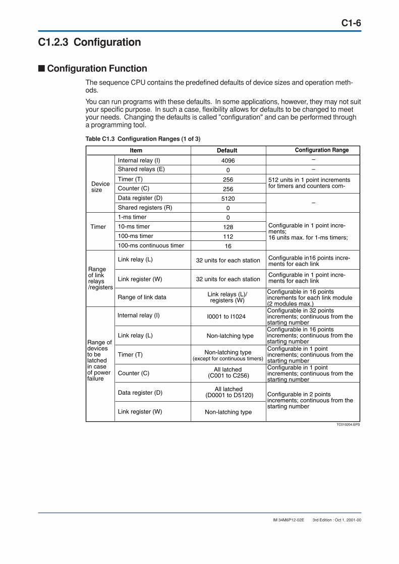
C1-6
IM 34M6P12-02E 3rd Edition : Oct 1, 2001-00
C1.2.3 Configuration
Configuration FunctionThe sequence CPU contains the predefined defaults of device sizes and operation meth-ods.
You can run programs with these defaults. In some applications, however, they may not suityour specific purpose. In such a case, flexibility allows for defaults to be changed to meetyour needs. Changing the defaults is called "configuration" and can be performed througha programming tool.
Table C1.3 Configuration Ranges (1 of 3)
Item
TC010204.EPS
Default
Internal relay (I) 4096
0
256
256
5120
0
0
128
112
16
Link register (W)
Link register (W)
Configuration Range
Shared relays (E)
Counter (C)
Data register (D)
Shared registers (R)
Link relay (L)
Link relay (L)
Timer (T)
Internal relay (I)
Counter (C)
Data register (D)
Timer (T)
Devicesize
Timer
1-ms timer
10-ms timer
100-ms timer
100-ms continuous timer
Rangeof linkrelays/registers
Range of link data Link relays (L)/registers (W)
Configurable in 16 points increments for each link module (2 modules max.)Configurable in 32 points increments; continuous from the starting numberConfigurable in 16 points increments; continuous from the starting numberConfigurable in 1 point increments; continuous from the starting numberConfigurable in 1 point increments; continuous from the starting number
Configurable in 2 points increments; continuous from the starting number
Range of devices to be latched in case of power failure
–
–
–
512 units in 1 point increments for timers and counters com-
Configurable in16 points incre-ments for each link
Configurable in 1 point incre-ments for each link
Configurable in 1 point incre-ments;16 units max. for 1-ms timers;
32 units for each station
32 units for each station
Non-latching type
I0001 to I1024
Non-latching type
Non-latching type(except for continuous timers)
All latched (C001 to C256)
All latched (D0001 to D5120)
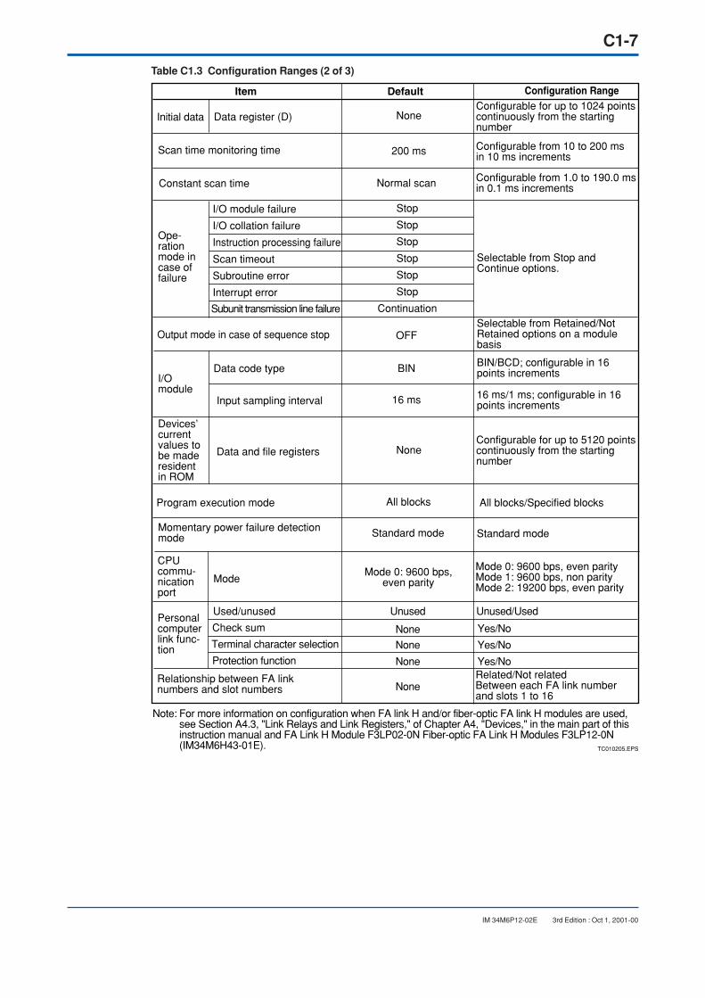
C1-7
IM 34M6P12-02E 3rd Edition : Oct 1, 2001-00
Table C1.3 Configuration Ranges (2 of 3)
Item
TC010205.EPS
Default Configuration Range
Data register (D)Configurable for up to 1024 points continuously from the starting number
Configurable from 10 to 200 ms in 10 ms increments
Configurable from 1.0 to 190.0 ms in 0.1 ms increments
Selectable from Stop and Continue options.
Selectable from Retained/Not Retained options on a module basis
Initial data
Ope-ration mode in case of failure
I/O module
Devices’ current values to be made resident in ROM
Momentary power failure detection mode Standard mode
None
None
200 msScan time monitoring time
Constant scan time Normal scan
I/O module failure
I/O collation failure
Instruction processing failure
Scan timeout
Subroutine error
Interrupt error
Subunit transmission line failure
Stop
Stop
Stop
Stop
Stop
Stop
Continuation
Output mode in case of sequence stop OFF
BIN
16 ms
BIN/BCD; configurable in 16 points increments
16 ms/1 ms; configurable in 16 points increments
Configurable for up to 5120 points continuously from the starting number
Standard mode
Data code type
Input sampling interval
Data and file registers
Program execution mode All blocks All blocks/Specified blocks
ModeMode 0: 9600 bps, even parityMode 1: 9600 bps, non parityMode 2: 19200 bps, even parity
Related/Not relatedBetween each FA link number and slots 1 to 16
Relationship between FA link numbers and slot numbers
CPU commu-nication port
Personal computer link func-tion
Mode 0: 9600 bps,even parity
Used/unused
Check sum
Terminal character selection
Protection function
Unused
None
None
None
None
Unused/Used
Yes/No
Yes/No
Yes/No
Note: For more information on configuration when FA link H and/or fiber-optic FA link H modules are used, see Section A4.3, "Link Relays and Link Registers," of Chapter A4, "Devices," in the main part of this instruction manual and FA Link H Module F3LP02-0N Fiber-optic FA Link H Modules F3LP12-0N (IM34M6H43-01E).

C1-8
IM 34M6P12-02E 3rd Edition : Oct 1, 2001-00
C1.2.4 Components and Their FunctionsThis subsection describes the LED indicators, their states, and the programming toolconnector on the front side of the sequence CPU module.
Table C1.4 summarizes combinations of the LED indicators as classified by the severity of failure.
FC010201.EPS
SP08-0P CPU
CPU module operation status LED indicators
RDY (= READY, green) --------------------On = Normal Off = Major failureRUN (= RUN, green) ---------------------- On = Program in progress Off = Program at a stopALM (= ALARM, yellow) ------------------ On = Minor failure Off = NormalERR (= ERROR, red) --------------------- On = Moderate failure Off = Normal
Major failure --------------- The CPU module is inoperable due to a hardware failure.
Moderate failure ---------- The CPU module cannot run or continue to run a program.
Minor failure --------------- The CPU module still can run or continue to run a program though it has detected a failure.
Programming tool connector ------------------- Connected to a personal computer.
A personal computer or a monitor can be connected to this connector when the personal computer link function is in use.
Table C1.4 LED Indicator Combinations Based on the Severity of Failure
Status Normal
On Off On On
On Off Off On
Off On or Off On or Off On
Off On On Off
MajorFailure
ModerateFailure
MinorFailureLED Indicator
RDY
RUN
ALM
ERRTC010207.EPS

C1-9
IM 34M6P12-02E 3rd Edition : Oct 1, 2001-00
C1.2.5 External Dimensions
83.2 582
100
F3SP08-0P
FC010202.EPS
Unit:mm
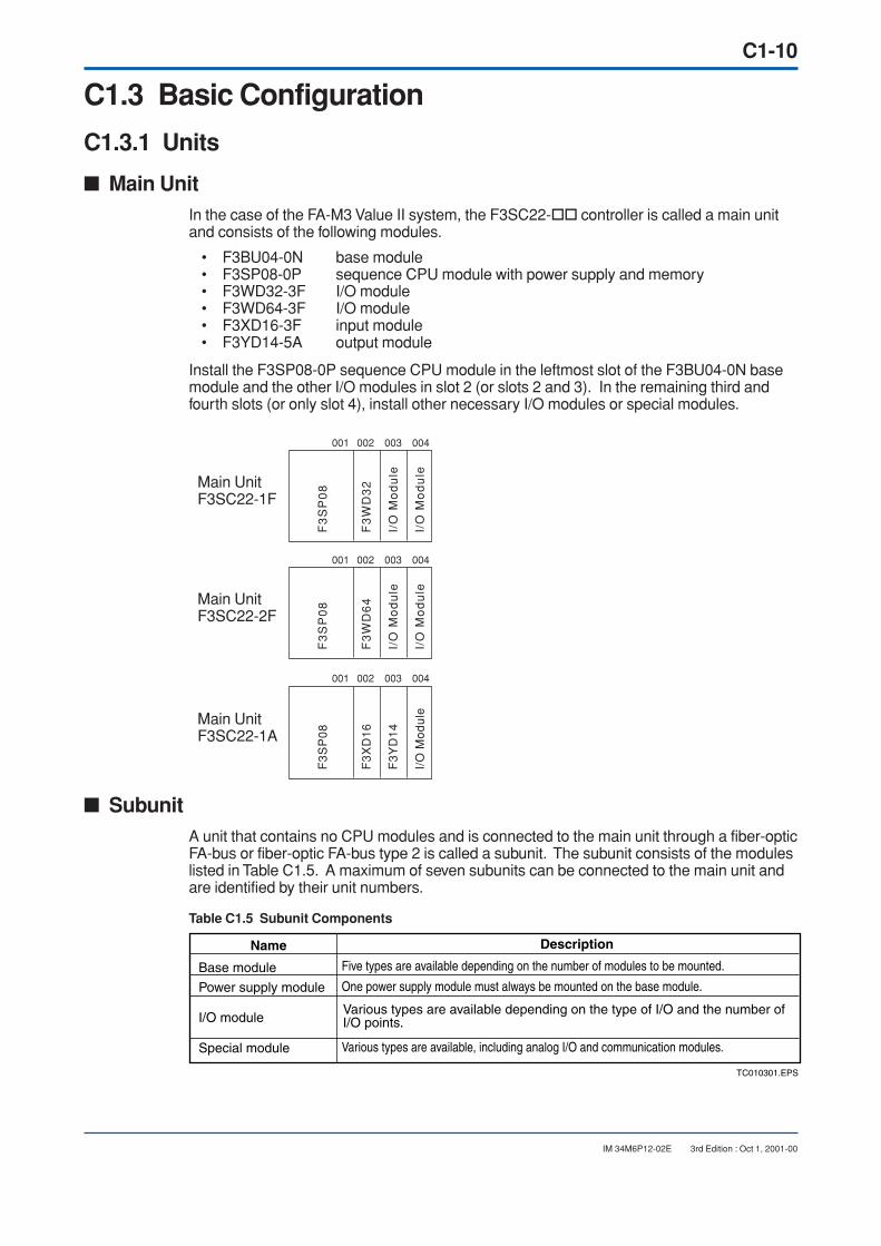
C1-10
IM 34M6P12-02E 3rd Edition : Oct 1, 2001-00
C1.3 Basic Configuration
C1.3.1 Units
Main UnitIn the case of the FA-M3 Value II system, the F3SC22- controller is called a main unitand consists of the following modules.
• F3BU04-0N base module• F3SP08-0P sequence CPU module with power supply and memory• F3WD32-3F I/O module• F3WD64-3F I/O module• F3XD16-3F input module• F3YD14-5A output module
Install the F3SP08-0P sequence CPU module in the leftmost slot of the F3BU04-0N basemodule and the other I/O modules in slot 2 (or slots 2 and 3). In the remaining third andfourth slots (or only slot 4), install other necessary I/O modules or special modules.
SubunitA unit that contains no CPU modules and is connected to the main unit through a fiber-opticFA-bus or fiber-optic FA-bus type 2 is called a subunit. The subunit consists of the moduleslisted in Table C1.5. A maximum of seven subunits can be connected to the main unit andare identified by their unit numbers.
Table C1.5 Subunit Components
Name Description
Base module Five types are available depending on the number of modules to be mounted.
One power supply module must always be mounted on the base module.
Various types are available, including analog I/O and communication modules.
Power supply module
I/O module
Special module
TC010301.EPS
Various types are available depending on the type of I/O and the number of I/O points.
Main UnitF3SC22-1F
F3
SP
08
F3
WD
32
I/O
Mo
du
le
I/O
Mo
du
le
Main UnitF3SC22-2F
F3
SP
08
F3
WD
64
I/O
Mo
du
le
I/O
Mo
du
le
Main UnitF3SC22-1A
F3
SP
08
F3
XD
16
F3
YD
14
I/O
Mo
du
le
001 002 003 004
001 002 003 004
001 002 003 004
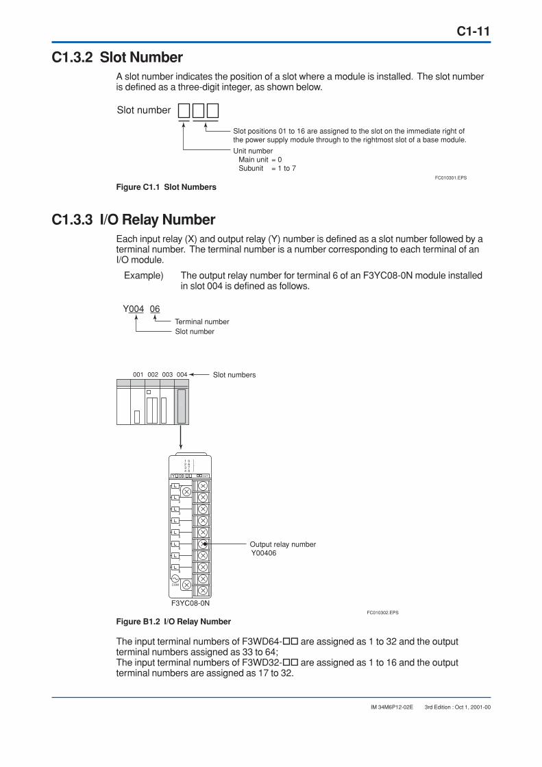
C1-11
IM 34M6P12-02E 3rd Edition : Oct 1, 2001-00
C1.3.2 Slot NumberA slot number indicates the position of a slot where a module is installed. The slot numberis defined as a three-digit integer, as shown below.
FC010301.EPS
Slot number
Slot positions 01 to 16 are assigned to the slot on the immediate right of the power supply module through to the rightmost slot of a base module.
Unit numberMain unit = 0Subunit = 1 to 7
Figure C1.1 Slot Numbers
C1.3.3 I/O Relay NumberEach input relay (X) and output relay (Y) number is defined as a slot number followed by aterminal number. The terminal number is a number corresponding to each terminal of anI/O module.
Example) The output relay number for terminal 6 of an F3YC08-0N module installedin slot 004 is defined as follows.
FC010302.EPS
Y
001 002 003 004
Y004 06Terminal numberSlot number
Slot numbers
Output relay number Y00406
OUT08-
F3YC08-0N
Figure B1.2 I/O Relay Number
The input terminal numbers of F3WD64- are assigned as 1 to 32 and the outputterminal numbers assigned as 33 to 64;The input terminal numbers of F3WD32- are assigned as 1 to 16 and the outputterminal numbers are assigned as 17 to 32.

Blank Page
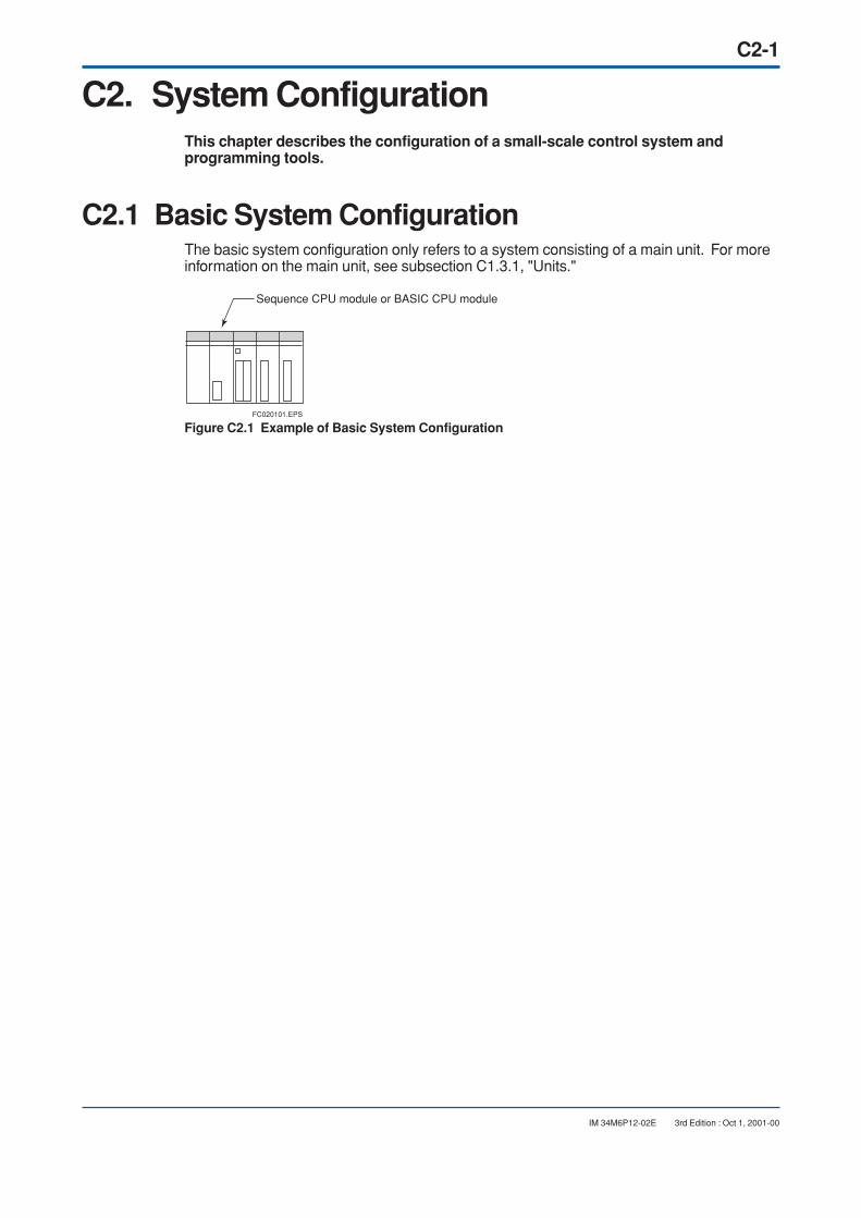
C2-1
IM 34M6P12-02E 3rd Edition : Oct 1, 2001-00
C2. System ConfigurationThis chapter describes the configuration of a small-scale control system andprogramming tools.
C2.1 Basic System ConfigurationThe basic system configuration only refers to a system consisting of a main unit. For moreinformation on the main unit, see subsection C1.3.1, "Units."
FC020101.EPS
Sequence CPU module or BASIC CPU module
Figure C2.1 Example of Basic System Configuration

C2-2
IM 34M6P12-02E 3rd Edition : Oct 1, 2001-00
C2.2 Extended System ConfigurationThe extended system configuration refers to a system configured by adding remote I/Omodules, a personal computer link module, and an FA link module to the basic system.
C2.2.1 Remote I/O SystemThe remote I/O system refers to a system configured using fiber-optic FA-bus or FA-bustype 2 communication modules.
The number of remote I/O points is included in the count of all I/O points.
FC020202.EPS
Main unit
Subunit
Subunit
Fiber-optic FA-bus type 2 module
Fiber-optic cable
Fiber-optic FA-bus type 2 module
Fiber-optic cable
Figure C2.2 Example of System Using Fiber-optic FA-bus Type 2 Modules
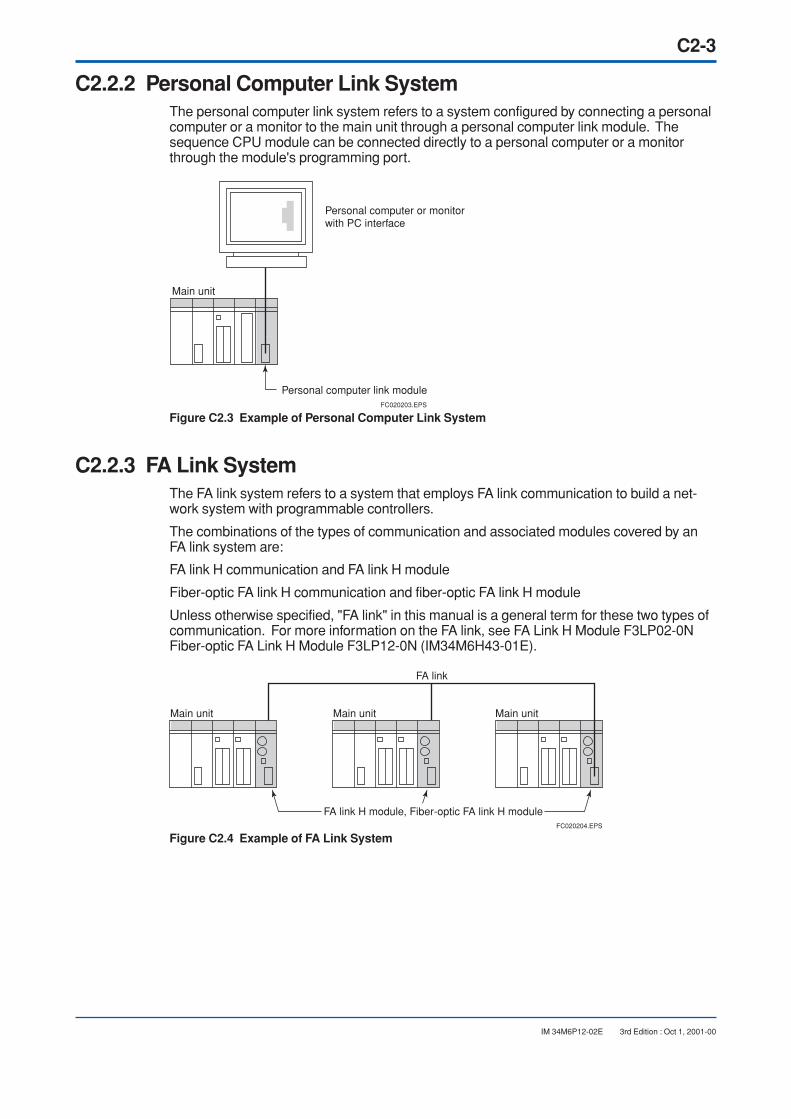
C2-3
IM 34M6P12-02E 3rd Edition : Oct 1, 2001-00
C2.2.2 Personal Computer Link SystemThe personal computer link system refers to a system configured by connecting a personalcomputer or a monitor to the main unit through a personal computer link module. Thesequence CPU module can be connected directly to a personal computer or a monitorthrough the module's programming port.
FC020203.EPS
Personal computer or monitor with PC interface
Main unit
Personal computer link module
Figure C2.3 Example of Personal Computer Link System
C2.2.3 FA Link SystemThe FA link system refers to a system that employs FA link communication to build a net-work system with programmable controllers.
The combinations of the types of communication and associated modules covered by anFA link system are:
FA link H communication and FA link H module
Fiber-optic FA link H communication and fiber-optic FA link H module
Unless otherwise specified, "FA link" in this manual is a general term for these two types ofcommunication. For more information on the FA link, see FA Link H Module F3LP02-0NFiber-optic FA Link H Module F3LP12-0N (IM34M6H43-01E).
FC020204.EPS
Main unit Main unit
FA link
Main unit
FA link H module, Fiber-optic FA link H module
Figure C2.4 Example of FA Link System

C2-4
IM 34M6P12-02E 3rd Edition : Oct 1, 2001-00
C2.3 Programming ToolsThe FA-M3 Programming Tool WideField and Ladder Diagram Support Program M3 areavailable as programming tools for the F3SP05-0P sequence CPU module.
C2.3.1 WideFieldThe table below presents an overview of WideField.
Description Software Model Supported CPUs
FA-M3 Programming Tool WideField SF610-JCW
F3SP05 F3SP35F3SP08 F3SP38F3SP21 F3SP53F3SP25 F3SP58F3SP28 F3FP36
TB020301.EPS
FC020301.EPS
Personal computer
Sequence CPU module
Figure C2.5 Overview of WideField
CAUTION
The R2.04 or a later version of FA-M3 Programming Tool WideFild is required to use theF3SP08-0P sequence CPU module.
Object LadderWideField defines "blocks" that compose a ladder program as "objects," a term commonlyused in the computing world. The object-oriented ladder language assumes responsibilityfor a given function and features a high degree of independence. Consequently, the lan-guage offers higher productivity and better maintainability than a structured programminglanguage. It is therefore effective for the reuse of ladder programs.
Features
Treatment as Components
Blocks can be reused as sheer components. Devices that are used only within a block aredefined separately. WideField eliminates the chance of using the same device twice andmakes it easy to recombine blocks.
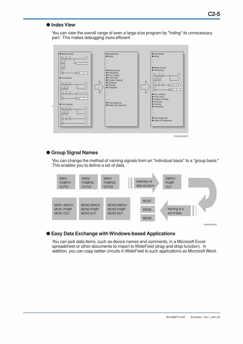
C2-5
IM 34M6P12-02E 3rd Edition : Oct 1, 2001-00
Index View
You can view the overall range of even a large-size program by "hiding" its unnecessarypart. This makes debugging more efficient
.
FC020302.EPS
I*****
I*****
I*****
I*****
Y*****
Y*****
Y*****
Y*****
I*****
I*****
I*****
I*****
I*****
I*****
I*****
I*****
I*****
Y*****
Y*****
I*****
I*****
I*****
I*****
I*****
I*****
I*****
I*****
I***** Y*****I***** I*****
CAL =
MOVE
+
I*****
I*****
I*****
I*****
Y*****
Y*****
I*****
I*****
I*****
I*****
I*****
CAL =
MOVE
+
CAL =
MOVE
+
Material feed Initialization Idling
Fault-diagnosis Power-off sequence
Material feed Preheating Flux coating Finish coat Fixation heating Cleaning Cooling Unloading
Preheating
Flux coating
•
•
•
•
•
•
Initialization Idling
Fault-diagnosis Power-off sequence
Material feed Preheating
•••
•••
Flux coating Finish coat Fixation heating Cleaning Cooling Unloading
Group Signal Names
You can change the method of naming signals from an "individual basis" to a "group basis."This enables you to define a set of data.
SW01POMP01OUT01
MCN1.SWICHMCN1.POMPMCN1.OUT
MCN2.SWICHMCN2.POMPMCN3.OUT
MCN3.SWICHMCN3.POMPMCN3.OUT
SW02POMP02OUT02
SW03POMP03OUT03
SWICHPOMPOUT
Definition of data structure
Naming of a set of data
MCN1
MCN2
MCN3
F040403.EPS
Easy Data Exchange with Windows-based Applications
You can pick data items, such as device names and comments, in a Microsoft Excelspreadsheet or other documents to import to WideField (drag-and-drop function). Inaddition, you can copy ladder circuits in WideField to such applications as Microsoft Word.

Blank Page
Toc-1
IM 34M6P12-02E
This appendix provides lists of special devices, as well as the formats ofdocumentation you will use when designing your system. These formattedsheets can be conveniently copied for use as standard forms in your systemdesign. There are four forms, as shown in the table of contents below.
CONTENTS
3rd Edition : Oct 1, 2001-00
IM 34M6P12-02E 3rd Edition
Sequence CPU Instruction Manual - Functions(for F3SP21, F3SP25 and F3SP35)
Appendix 1. Special Relays (M) .................................................................App.1-1Appendix 1.1 Block Start Status........................................................................... App.1-1
Appendix 1.2 Utility Relays ................................................................................... App.1-2
Appendix 1.3 Sequence Operation and Mode Status Relays ............................. App.1-4
Appendix 1.4 Self-diagnosis Status Relays ......................................................... App.1-5
Appendix 1.5 FA Link Module Status Relays ....................................................... App.1-7
Appendix 2. Special Registers (Z) .............................................................App.2-1Appendix 2.1 Sequence Operation Status Registers .......................................... App.2-1
Appendix 2.2 Self-diagnosis Status Registers .................................................... App.2-2
Appendix 2.3 Utility Registers .............................................................................. App.2-4
Appendix 2.4 FA Link Module Status Registers .................................................. App.2-5
Appendix 2.5 CPU Module Status Registers ....................................................... App.2-6
Appendix 3. Forms for System Design .....................................................App.3-1 Program Coding Sheet ..................................................................................... App.3-1
Relay Devices Assignment Table ..................................................................... App.3-2
Register Devices Assignment Table ................................................................ App.3-3
Timer/Counter Setpoints Table ......................................................................... App.3-4

Blank Page

App.1-1
IM 34M6P12-02E 3rd Edition : Oct 1, 2001-00
Appendix 1. Special Relays (M)Special relays have specific functions, such as indicating the internal state of a CPU ordetecting errors. In programs, these relays are used mainly for contacts a and b.
Appendix 1.1 Block Start StatusBlock start status relays indicate which block is running when the selected blocks are beingexecuted.
These relays are numbered in ascending order as M001, M002, . . ., to correlate with block1, block 2, ...
Table Appendix 1.1 Block Start Status
Item Description
AP040401.EPS
CPU Module
F3SP21, F3SP25,F3SP35 (Note)
F3SP28,F3SP38,F3SP53,F3SP58
Relay Number Name Function Remarks
M0001 to M0032
Block n startstatus relay
ON : RunOFF: Stop
Indicate whether block n is in progress or at a stop when blocks are selected and executed.
Note: The start status relays assigned to blocks 1 to 32 are M0001 to M0032 and M2001 to M2032, where the values of M0001 to M0032 are the same as those of M2001 to M2032. Similarly, start status relays M2033 to M3024 are assigned to blocks 33 to 1024.
M001 to M0016
M2001 to M3024
CAUTION
Do not write to a special relay, including those not listed in the table above (e.g., M067 toM128), unless otherwise stated. This is because they are used by the CPU module for thesystem. If you inadvertently write to these relays, a failure such as a system shutdown mayoccur. (The use of a forced set/reset instruction in debug mode is also prohibited.)

App.1-2
IM 34M6P12-02E 3rd Edition : Oct 1, 2001-00
Appendix 1.2 Utility RelaysUtility relays are used to provide timing in a program or give instructions to the CPU.
Table Appendix 1.2 Utility Relays
Always ON
Always OFF
No.
Item Utility Relays
Name Function Description
On-for-one-scan-at-start-of-operation
M033
M034
M035
M036
M037
M038
M039
M040
M041
M042
M047
M048
M066
M097
ONOFF
ONOFF
1 scan
0.005s0.005s
0.01s0.01s
0.05s0.05s
0.1s0.1s
0.5s0.5s
1s1s
30s30s
0.01-sec clock
0.02-sec clock
0.1-sec clock
0.2-sec clock
1-sec clock
2-sec clock
1-min clock
1-ms clock
2-ms clock
0.5s0.5s
1ms1ms
Used for an initialization process or as a dummy contact in a program.
Turns on for one scan only after the start of a program.
Generates a clock pulse with a 0.01-sec period.
Generates a clock pulse with a 0.02-sec period.
Generates a clock pulse with a 0.1-sec period.
AP010101.EPS
Generates a clock pulse with a 0.2-sec period.
Generates a clock pulse with a 1-sec period.
Generates a clock pulse with a 2-sec period.
Generates a clock pulse with a 1-min period.
Generates a clock pulse with a 1-msec period.
Generates a clock pulse with a 2-msec period.
(Note)
(Note)
ON: Normal transmission line or no fiber-optic FA-bus installedOFF: Unspecified or abnormal transmission line
ON: When the block starts.OFF: In all other cases.
Turns on for one scan when the sensor control block starts (at the first execution of the sensor control block).
Normal subunit transmission line
On for one scan at CB startup(Note)
Note: Only available with the F3SP28, F3SP38, F3SP53 and F3SP58.

App.1-3
IM 34M6P12-02E 3rd Edition : Oct 1, 2001-00
CAUTION
The utility relay M066 “normal subunit transmission line” is only available with the Rev.8 orlater version of the F3SP21, F3SP25 and F3SP35.
See Also
Fiber-optic FA-bus Module and Fiber-optic FA-bus Type 2 Module (IM34M6H45-01E), formore information on the M066 utility relay (Normal Subunit Transmission Line).
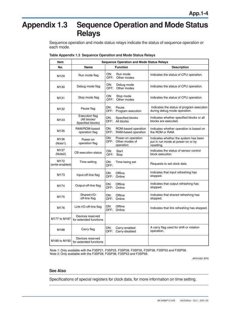
App.1-4
IM 34M6P12-02E 3rd Edition : Oct 1, 2001-00
Appendix 1.3 Sequence Operation and Mode StatusRelays
Sequence operation and mode status relays indicate the status of sequence operation oreach mode.
Table Appendix 1.3 Sequence Operation and Mode Status Relays
Run mode flag
Debug mode flag
No.
Item Sequence Operation and Mode Status Relays
Name Function Description
Stop mode flag
M129
M130
M131
M132
M133
M135
M136
M137
M172
M173
M174
M175
M176
M177 to M187
M188
M189 to M192
Pause flag
Execution flag(All blocks/
Specified blocks)
RAM/ROM-based operation flag
Time setting
Input-off-line flag
Output-off-line flag
Shared-I/O-off-line flag
Link-I/O-off-line flag
Devices reservedfor extended functions
Devices reservedfor extended functions
Carry flag
Indicates the status of CPU operation.
Indicates the status of CPU operation.
Indicates the status of CPU operation.
Indicates the status of program execution during debug mode operation.
Indicates whether specified blocks or all blocks are executed.
Indicates whether operation is based on the ROM or RAM.
Indicates the status of sensor control block execution.
Indicates that input refreshing has stopped.
Indicates that output refreshing has stopped.
Indicates that shared refreshing has stopped.
A carry flag used for shift or rotation operation.
Indicates that link refreshing has stopped.
Requests to set clock data
Indicates whether the system has been put in run mode at power-on or by resetting.
AP010301.EPS
Power-onoperation flag
CB execution status
(write-enabled)
(Note1)
(Note2)
ON: Run modeOFF: Other modes
ON: StartOFF: Stop
ON: Debug modeOFF: Other modes
ON: Stop modeOFF: Other modes
ON: PauseOFF: Program execution
ON: Specified blocksOFF: All blocks
ON: ROM-based operationOFF: RAM-based operation
ON: Power-on operationOFF: Other modes of
operation
ON: Time being setOFF:
ON: OfflineOFF: Online
ON: OfflineOFF: Online
ON: OfflineOFF: Online
ON: OfflineOFF: Online
ON: Carry-enabledOFF: Carry-disabled
Note 1: Only available with the F3SP21, F3SP25, F3SP28, F3SP35, F3SP38, F3SP53 and F3SP58.Note 2: Only available with the F3SP28, F3SP38, F3SP53 and F3SP58.
See Also
Specifications of special registers for clock data, for more information on time setting.

App.1-5
IM 34M6P12-02E 3rd Edition : Oct 1, 2001-00
Appendix 1.4 Self-diagnosis Status RelaysSelf-diagnosis status relays indicate the results of self-diagnostics by the sequence CPU.
Table Appendix 1.4 Self-diagnosis Status Relays
Self-diagnosis error
Battery failure
No.
Item Self-diagnosis Status Relays
Name Function Description
Momentarypower failure
M193
M194
M196
M197
M198
M199
M200
M201
M202
M203
M204
CPU-to-CPUcommunication failure
Existence of CPU1
Existence of CPU2
Existence of CPU3
Instructionprocessing error
I/O collation error
I/O module failure
Scan time-out
Subunit transmission line fai lure
Switchover in subunittransmission line
CB scan timeout
CPU-2 sequenceprogram execution
CPU-3 sequenceprogram execution
CPU-4 sequenceprogram execution
CPU-1 sequenceprogram execution
Error information is stored in special registers Z17 to Z19 for updating the results of self-diagnosis.
Indicates that a momentary failure has occurred.
Indicates that a communication failure has occurred in shared relays/registers.
Indicates a failure in backup batteries.
Indicates whether or not a CPU exists in slot 1.
Indicates whether or not a CPU exists in slot 2.
Indicates whether or not a CPU exists in slot 3.
Indicates that the state of module installation is not consistent with the program.
Indicates that access to I/O modules is not possible. The slot number of the module in question is stored in special registers Z33 to Z40.
Indicates that the scan has exceeded the scan time monitoring time.
Indicates that it is not possible to sustain the execution interval of the sensor control block.
Indicates whether a sequence program for a CPU in slot 1 is running or at a stop.
Indicates whether a sequence program for a CPU in slot 1 is running or at a stop.
Indicates whether a sequence program for a CPU in slot 1 is running or at a stop.
Indicates whether a sequence program for a CPU in slot 1 is running or at a stop.
The slot number of the fiber-optic FA-bus module in question is stored in special registers Z89 to Z96 if a failure occurs in the module.
Information on an error that may occur during instruction processing is stored in special registers Z22 to Z24.
Indicates whether or not a CPU exists in slot 4.
AP010401.EPS
Existence of CPU4
ON: An error is found.OFF: No error is found
ON: An error is found.OFF: No error is found
Note 1: Only available with the F3SP21, F3SP25, F3SP28, F3SP35, F3SP38, F3SP53 and F3SP58.Note 2: Only available with the F3SP28, F3SP38, F3SP53 and F3SP58.
(Note1)
(Note1)
(Note1)
(Note1)
ON: Abnormal.OFF: Normal.
ON: Abnormal.OFF: Normal.
ON: Abnormal.OFF: Normal.
ON: Abnormal.OFF: Normal.
ON: Abnormal.OFF: Normal.
ON: Abnormal.OFF: Normal.
ON: A momentary powerfailure is found.
OFF: No momentary powerfailure is found.
ON: Exists.OFF: Does not exist.
ON: Exists.OFF: Does not exist.
ON: Exists.OFF: Does not exist.
ON: Exists.OFF: Does not exist.
ON: Abnormaltransmission line.
OFF: Unspecified ornormaltransmission line
ON: Abnormaltransmission line.
OFF: Unspecified ornormaltransmission line
ON: Executes the program.OFF: Stops the program.
ON: Executes the program.OFF: Stops the program.
ON: Executes the program.OFF: Stops the program.
ON: Executes the program.OFF: Stops the program.
M195
M225
M226
M227
M228
M210
M211
M212

App.1-6
IM 34M6P12-02E 3rd Edition : Oct 1, 2001-00
CAUTION
The M210 (Subunit Transmission Line Failure) and M211 (Switchover in SubunitTransmission Line) self-diagnosis relays are only available with the Rev.8 or a later versionof the F3SP21, F3SP25 and F3SP35.
See Also
Fiber-optic FA-bus Module and Fiber-optic FA-bus Type 2 Module (IM34M6H45-01E), formore information on the M210 (Subunit Transmission Line Failure) and M211 (Switchoverin Subunit Transmission Line) self-diagnosis relays.

App.1-7
IM 34M6P12-02E 3rd Edition : Oct 1, 2001-00
Appendix 1.5 FA Link Module Status RelaysFA Link module status relays indicate the status of FA link.
See Also
Special relays/registers sections of FA Link H Module F3LP02-0N Fiber-optic FA Link HModule F3LP12-0N (IM34M5H43-01E), for more information on these FA link modulestatus relays.
Table Appendix 1.5 FA Link Module Status Relays
Item FA Link Module Status Relays
AP010501.EPS
CPU Module
F3SP21,F3SP25F3SP35
Relay Number Name Function Remarks
M257 to M480
FA link failure ON: Abnormal.OFF: Normal.
Indicate the status of FA link.M257 to M480
M8321 to M8992
F3SP28, F3SP38
F3SP53, F3SP58

Blank Page

App.2-1
IM 34M6P12-02E 3rd Edition : Oct 1, 2001-00
Appendix 2. Special Registers (Z)Special registers have specific functions, such as indicating the internal state of aprogrammable controller or detecting errors.
Appendix 2.1 Sequence Operation Status RegistersSequence operation status registers indicate the status of sequence operation.
Table Appendix 2.1 Sequence Operation Status Registers
Scan time(Run mode)
Minimum scan time(Run mode)
No.
Type Sequence Operation Status Registers
Name Stored Data Description
Maximum scan time(Run mode)
Z001
Z002
Z003
Z004
Z005
Z006
Z007
Z008
Z009
Scan time(Debug mode)
Minimum scan time(Debug mode)
Maximum scan time(Debug mode)
Peripheral-processscan time
Minimum peripheral-process scan time
Maximum peripheral-process scan time
Stores the latest scan time in 100-µs increments.
Allows the latest scan time to be read in 100-µs increments if it is shorter than the minimum scan time.Allows the latest scan time to be read in 100-µs increments if it is longer than the maximum scan time.
Stores the latest scan time in 100-µs increments.
Allows the latest scan time to be read in 100-µs increments if it is shorter than the minimum scan time.Allows the latest scan time to be read in 100-µs increments if it is longer than the maximum scan time.
AP020101.EPS
Stores the latest scan time in 100-µs increments.(Tolerance: Scan time of one control process)
Allows the latest scan time to be read in 100-µs increments if it is shorter than the minimum scan time.(Tolerance: Scan time of one control process)
Allows the latest scan time to be read in 100-µs increments if it is longer than the maximum scan time.(Tolerance: Scan time of one control process)
Latest scan time
Minimum scan time
Maximum scan time
Minimum scan time
Maximum scan time
Minimum scan time
Maximum scan time
Latest scan time
Latest scan time
CAUTION
Do not write to a special register, including those not listed in the table above (e.g., Z010 toZ016), unless otherwise stated. This is because they are used by the CPU module for thesystem. If you inadvertently write to these registers, a failure such as a system shutdownmay occur.
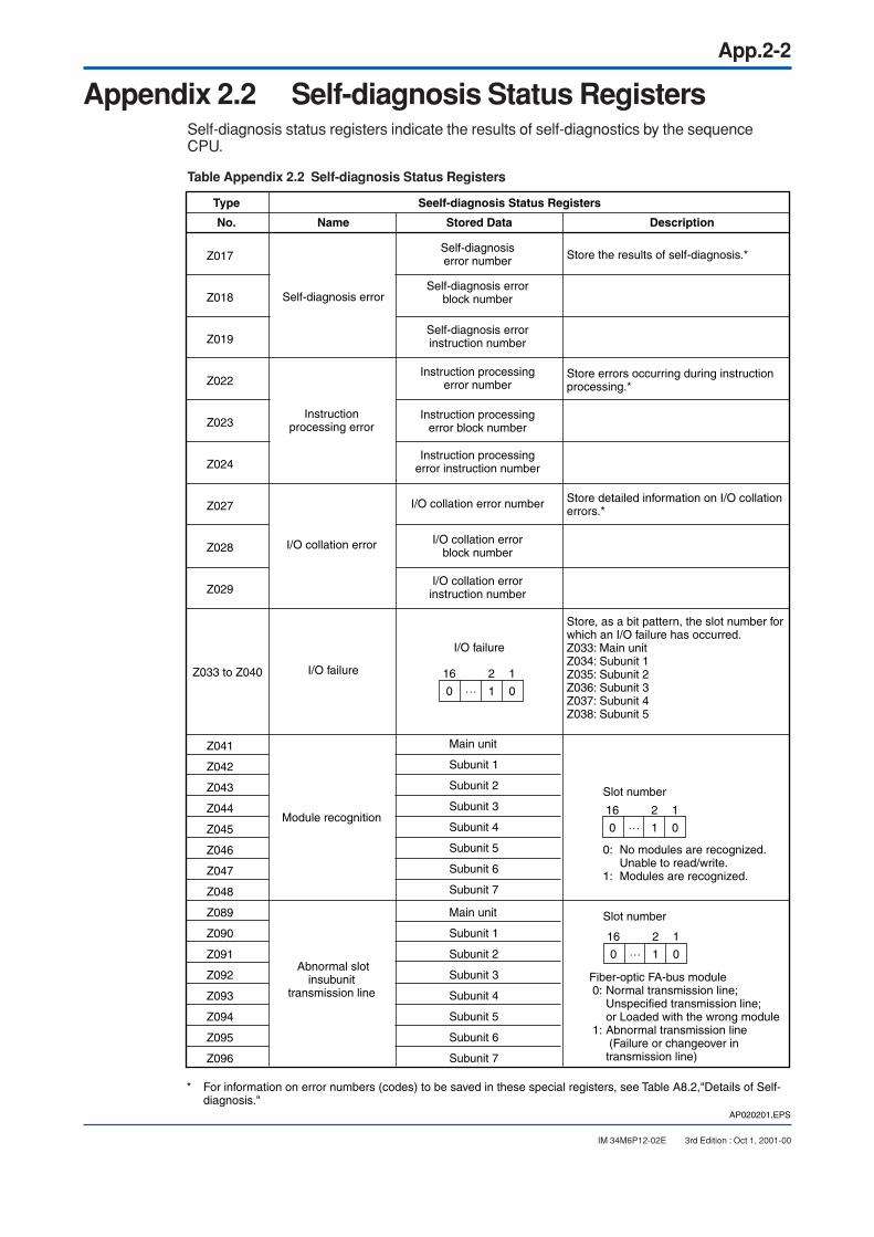
App.2-2
IM 34M6P12-02E 3rd Edition : Oct 1, 2001-00
Appendix 2.2 Self-diagnosis Status RegistersSelf-diagnosis status registers indicate the results of self-diagnostics by the sequenceCPU.
Table Appendix 2.2 Self-diagnosis Status Registers
Self-diagnosis error
No.
Type Seelf-diagnosis Status Registers
Name Stored Data Description
Z017
Z018
Z019
Z022
Z023
Z024
Z027
Z028
Z029
Z041
Z042
Z043
Z044
Z045
Z046
Z047
Z048
Z089
Z090
Z091
Z092
Z093
Z094
Z095
Z096
Instructionprocessing error
I/O collation error
I/O failure
Module recognition
Abnormal slotinsubunit
transmission line
Store the results of self-diagnosis.*
Store errors occurring during instruction processing.*
AP020201.EPS
Store detailed information on I/O collation errors.*
Store, as a bit pattern, the slot number for which an I/O failure has occurred.Z033: Main unitZ034: Subunit 1Z035: Subunit 2Z036: Subunit 3Z037: Subunit 4Z038: Subunit 5
* For information on error numbers (codes) to be saved in these special registers, see Table A8.2,"Details of Self-diagnosis."
Self-diagnosiserror number
Self-diagnosis errorblock number
Self-diagnosis errorinstruction number
I/O collation errorblock number
I/O collation errorinstruction number
I/O failure
Instruction processingerror block number
Instruction processingerror instruction number
Instruction processingerror number
I/O collation error number
Z033 to Z040
16 2 1
0 1 0…
16 2 1
0 1 0…
Main unit
Subunit 1
Subunit 2
Subunit 3
Subunit 4
Subunit 5
Subunit 6
Subunit 7
Main unit
Subunit 1
Subunit 2
Subunit 3
Subunit 4
Subunit 5
Subunit 6
Subunit 7
Slot number
Slot number
0: No modules are recognized. Unable to read/write.1: Modules are recognized.
Fiber-optic FA-bus module 0: Normal transmission line; Unspecified transmission line;
or Loaded with the wrong module 1: Abnormal transmission line
(Failure or changeover in transmission line)
16 2 1
0 1 0…

App.2-3
IM 34M6P12-02E 3rd Edition : Oct 1, 2001-00
CAUTION
• The Z041 to Z048 (Module Recognition) self-diagnosis status registers are onlyavailable with the Rev.8 or later version of the F3SP21, F3SP25 and F3SP35.
• The Z089 to Z096 (Abnormal Slot in Subunit Transmission Line) self-diagnosis statusregisters are only available with the Rev.8 or later version of the F3SP21, F3SP25 andF3SP35.
See Also
Fiber-optic FA-bus Module and Fiber-optic FA-bus Type 2 Module (IM34M6H45-01E), formore information on the Z089 to Z096 special registers (Abnormal Slot in SubunitTransmission Line).
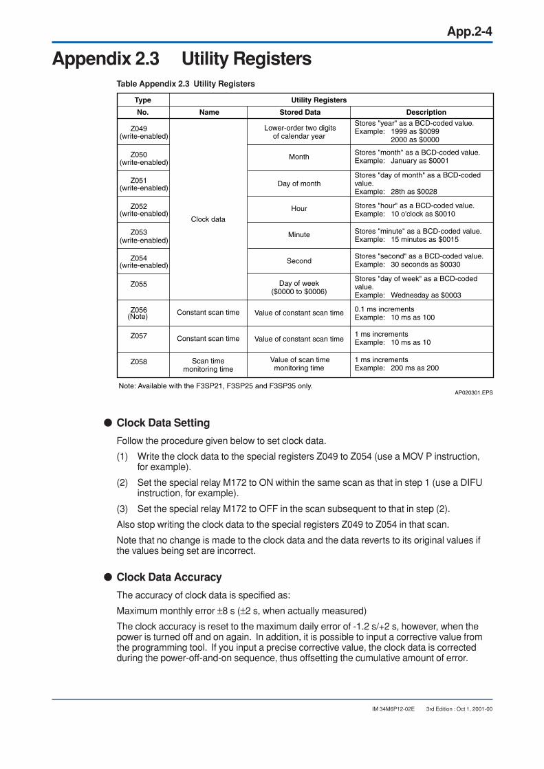
App.2-4
IM 34M6P12-02E 3rd Edition : Oct 1, 2001-00
Appendix 2.3 Utility RegistersTable Appendix 2.3 Utility Registers
Clock data
No.
Type Utility Registers
Name Stored Data Description
Z049
Z050
Z051
Z052
Z053
Z054
Z055
Z056
Z057
Z058
Stores "month" as a BCD-coded value.Example: January as $0001
Stores "day of month" as a BCD-coded value.Example: 28th as $0028
Stores "hour" as a BCD-coded value.Example: 10 o'clock as $0010
Stores "minute" as a BCD-coded value.Example: 15 minutes as $0015
0.1 ms incrementsExample: 10 ms as 100
1 ms incrementsExample: 10 ms as 10
1 ms incrementsExample: 200 ms as 200
Stores "second" as a BCD-coded value.Example: 30 seconds as $0030
Stores "day of week" as a BCD-coded value.Example: Wednesday as $0003
Stores "year" as a BCD-coded value.Example: 1999 as $0099
2000 as $0000
Lower-order two digitsof calendar year
Month
Day of month
Value of constant scan time
Value of constant scan time
Value of scan timemonitoring time
Minute
Second
Day of week($0000 to $0006)
Hour
(write-enabled)
(write-enabled)
(write-enabled)
(write-enabled)
(write-enabled)
(write-enabled)
(Note) Constant scan time
Constant scan time
Scan timemonitoring time
Note: Available with the F3SP21, F3SP25 and F3SP35 only.AP020301.EPS
Clock Data Setting
Follow the procedure given below to set clock data.
(1) Write the clock data to the special registers Z049 to Z054 (use a MOV P instruction,for example).
(2) Set the special relay M172 to ON within the same scan as that in step 1 (use a DIFUinstruction, for example).
(3) Set the special relay M172 to OFF in the scan subsequent to that in step (2).
Also stop writing the clock data to the special registers Z049 to Z054 in that scan.
Note that no change is made to the clock data and the data reverts to its original values ifthe values being set are incorrect.
Clock Data Accuracy
The accuracy of clock data is specified as:
Maximum monthly error ±8 s (±2 s, when actually measured)
The clock accuracy is reset to the maximum daily error of -1.2 s/+2 s, however, when thepower is turned off and on again. In addition, it is possible to input a corrective value fromthe programming tool. If you input a precise corrective value, the clock data is correctedduring the power-off-and-on sequence, thus offsetting the cumulative amount of error.
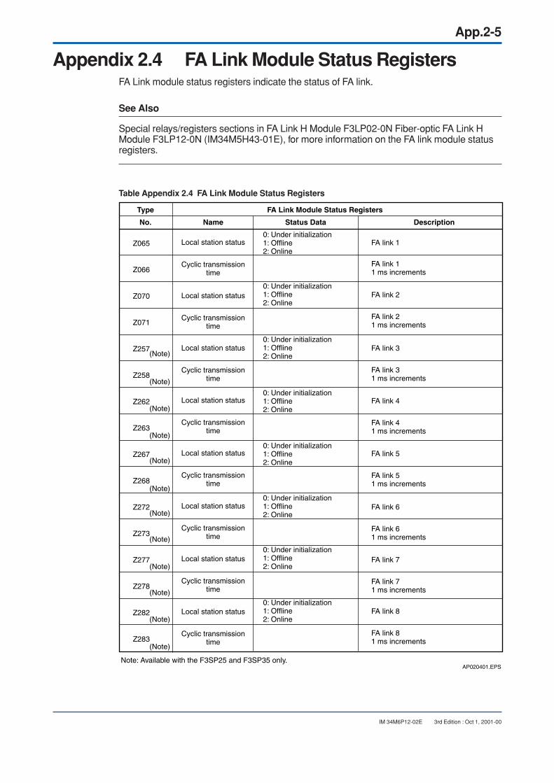
App.2-5
IM 34M6P12-02E 3rd Edition : Oct 1, 2001-00
Appendix 2.4 FA Link Module Status RegistersFA Link module status registers indicate the status of FA link.
See Also
Special relays/registers sections in FA Link H Module F3LP02-0N Fiber-optic FA Link HModule F3LP12-0N (IM34M5H43-01E), for more information on the FA link module statusregisters.
Table Appendix 2.4 FA Link Module Status Registers
Local station status
Cyclic transmissiontime
Local station status
Cyclic transmissiontime
Local station status
Cyclic transmissiontime
Local station status
Cyclic transmissiontime
Local station status
Cyclic transmissiontime
Local station status
Cyclic transmissiontime
Local station status
Cyclic transmissiontime
Local station status
Cyclic transmissiontime
No.
Type FA Link Module Status Registers
Name Status Data Description
Z065
Z066
Z070
Z071
Z257
Z258
Z262
Z263
Z267
Z268
Z272
Z273
Z277
Z278
Z282
Z283
AP020401.EPS
0: Under initialization1: Offline2: Online
0: Under initialization1: Offline2: Online
0: Under initialization1: Offline2: Online
0: Under initialization1: Offline2: Online
0: Under initialization1: Offline2: Online
0: Under initialization1: Offline2: Online
0: Under initialization1: Offline2: Online
0: Under initialization1: Offline2: Online
FA link 2
FA link 1
FA link 1 1 ms increments
FA link 2 1 ms increments
FA link 3
FA link 3 1 ms increments
FA link 4
FA link 4 1 ms increments
FA link 5
FA link 5 1 ms increments
FA link 6
FA link 6 1 ms increments
FA link 7
(Note)
(Note)
(Note)
(Note)
(Note)
(Note)
(Note)
(Note)
(Note)
(Note)
(Note)
(Note)
FA link 7 1 ms increments
FA link 8
FA link 8 1 ms increments
Note: Available with the F3SP25 and F3SP35 only.
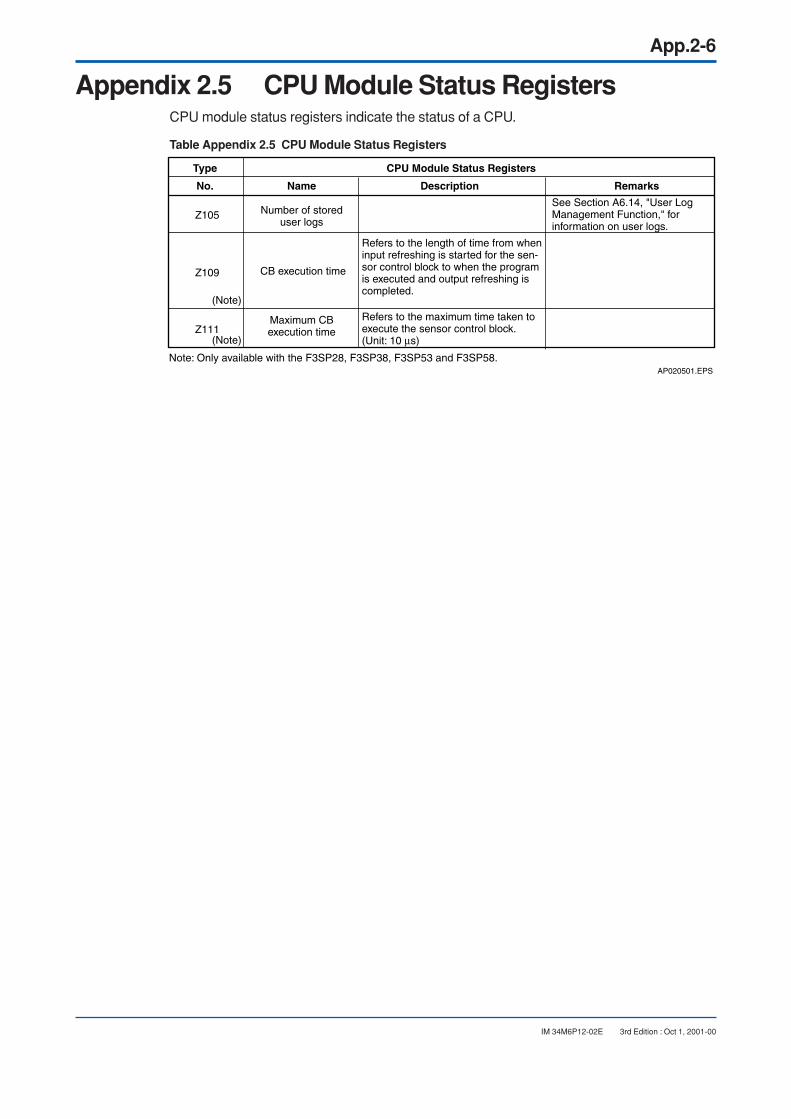
App.2-6
IM 34M6P12-02E 3rd Edition : Oct 1, 2001-00
Appendix 2.5 CPU Module Status RegistersCPU module status registers indicate the status of a CPU.
Table Appendix 2.5 CPU Module Status Registers
Number of storeduser logs
CB execution time
Maximum CBexecution time
Z105
Z109
Z111
(Note)
(Note)
No.
Type CPU Module Status Registers
Name Description Remarks
AP020501.EPS
See Section A6.14, "User Log Management Function," for information on user logs.
Refers to the length of time from when input refreshing is started for the sen-sor control block to when the program is executed and output refreshing is completed.
Refers to the maximum time taken to execute the sensor control block.(Unit: 10 µs)
Note: Only available with the F3SP28, F3SP38, F3SP53 and F3SP58.

App.3-1
IM 34M6P12-02E 3rd Edition : Oct 1, 2001-00
Appendix 3. Forms for System Design Program Coding Sheet
System Name
Model Drawing No.
Approved by
Checked by
Prepared by
SheetNo.
0
1
2
3
4
5
6
7
8
9
0
1
2
3
4
5
6
7
8
9
0
1
2
3
4
5
6
7
8
9
0
Instruction No. Instruction Operand Remarks
TAP0301.EPS

App.3-2
IM 34M6P12-02E 3rd Edition : Oct 1, 2001-00
Relay Devices Assignment Table
System Name
Model Drawing No.
Approved by
Checked by
Prepared by
SheetNo.
1
2
3
4
5
6
7
8
9
0
1
2
3
4
5
6
7
8
9
0
1
2
3
4
5
6
7
8
9
0
1
2
Device No. Signal Name Device No. Signal Name
TAP0302.EPS
Description Description
3
4
5
6
7
8
9
0
1
2
3
4
5
6
7
8
9
0
1
2
3
4
5
6
7
8
9
0
1
2
3
4
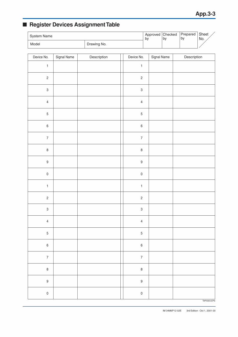
App.3-3
IM 34M6P12-02E 3rd Edition : Oct 1, 2001-00
Register Devices Assignment Table
System Name
Model Drawing No.
Approved by
Checked by
Prepared by
SheetNo.
1
2
3
4
5
6
7
8
9
0
1
2
3
4
5
6
7
8
9
0
Device No. Signal Name Device No. Signal Name
TAP0303.EPS
Description Description
1
2
3
4
5
6
7
8
9
0
1
2
3
4
5
6
7
8
9
0

App.3-4
IM 34M6P12-02E 3rd Edition : Oct 1, 2001-00
Timer/Counter Setpoints Table
System Name
Model Drawing No.
Approved by
Checked by
Prepared by
SheetNo.
1
2
3
4
5
6
7
8
9
0
1
2
3
4
5
6
7
8
9
0
1
2
3
4
5
6
7
8
9
0
1
2
Device No. Setpoint
TAP0304.EPS
Signal Name Description

Index-1
IM 34M6P12-02E
Index
3rd Edition : Oct 1, 2001-00
IM 34M6P12-02E 3rd Edition
FA-M3Sequence CPU Instruction Manual - Functions(for F3SP21, F3SP25 and F3SP35)
Number100-ms continuous timer ................................... A4-29100-ms timer ..................................................... A4-2910-ms timer ....................................................... A4-291-ms timer ......................................................... A4-29
Bbasic system configuration ............... A2-1, B2-1, C2-1block ................................................................... A5-3block protection ................................................. A6-18block start status ............................................... A4-22
Cclearing device .................................................... A6-3clearing memory ................................................. A6-3command.......................................................... A6-39communication procedure................................. A6-37computation method ........................................... A3-6configuration .................................... A1-7, B1-6, C1-6constant scan time .............................................. A6-5counter ............................................................. A4-30CPU module status ........................................... A4-44CPU service ..................................................... A3-14current value ..................................................... A6-16
Ddata code type, specifying ................................... A4-3data register (D) ................................................ A4-32data value, changing ......................................... A6-16debug mode ...............................................A3-1, A6-3device ................................................................. A4-1device list ......................................... A1-5, B1-5, C1-5device management function ............................ A6-46DIO (input/output module) setup ......................... A4-3
Eexclusive access right ....................................... A6-26executable program ............................................ A5-4executable program protection .......................... A6-17executing all blocks ............................................. A6-6
executing specified blocks ................................... A6-7extended shared register (R) ............................. A4-36extended shared relay (E) ..........................A4-6, A4-9extended system configuration.................. B2-2, C2-2
FF3SP05 .............................................................. B1-1F3SP08 ..............................................................C1-1F3SP21 .............................................................. A1-1F3SP25 .............................................................. A1-1F3SP35 .............................................................. A1-1FA link module status .............................A4-26, A4-43FA link system .................................. A2-4, B2-3, C2-3FA-M3 Value ....................................................... B1-1FA-M3 Value II ....................................................C1-1file register (B) .................................................. A4-46forced reset ....................................................... A6-15forced set .......................................................... A6-15
II/O address allocation ......................................... A4-2immediate detection mode .................................. A3-3index register (V) ............................................... A4-45initial data ......................................................... A4-38interrupt processing .......................................... A3-17interrupt processing control ............................... A3-18input relay (X) ..................................................... A4-1input sampling interval ........................................ A4-3input/output processing ....................................... A3-8input/output relay number .......... A1-17, B1-11, C1-11internal relay (I) ..........................................A4-5, A4-9interrupt program ................................................ A5-8
Lladder diagram support program M3 ..........A2-7, B2-6link refresh ........................................................ A3-15link register (W) ......................................A4-16, A4-21link relay (L) ...........................................A4-11, A4-21link service ........................................................ A3-11

Index-2
IM 34M6P12-02E 3rd Edition : Oct 1, 2001-00
Mmacro instruction .............................................. A6-47main routine program .......................................... A5-6main unit .................................... A1-14, B1-10, C1-10minor failure ...................................................... A8-10mnemonic language ........................................... A5-2mode status ...................................................... A4-24moderate failure ................................................ A8-10momentary power failure detection mode ............ A3-3multi-CPU system configuration .......................... A2-1
Ooperation in case of complete power failure ......... A3-4operation in case of momentary power failure ..... A3-3operation mode ..........................................A3-1, A6-3operation mode of CPU ...................................... A3-1output hold .......................................................... A4-4output relay (Y) ................................................... A4-2output reset ......................................................... A4-4
Ppartial operation ................................................ A6-15PC link function ................................................. A6-31PC link system ................................. A2-3, B2-3, C2-3program memory ................................................ A5-9programming language ....................................... A5-1programming tool ............................. A2-5, B2-4, C2-4
RRAS function ....................................................... A8-1remote I/O system ........................... A2-3, B2-2, C2-2reset ................................................................... A4-4response........................................................... A6-39response delay ................................................... A3-9ROM Clear function .......................................... A6-25ROM Copy function ........................................... A6-25ROM Cross-check function ............................... A6-25ROM resident ................................................... A6-20ROM Transfer function ...................................... A6-25ROM Writer function ......................................... A6-20
Ssampling trace function ..................................... A6-27scan operation .................................................. A6-14scan time ............................................................ A7-1scan time monitoring time, setting ....................... A7-2self diagnosis ...................................................... A8-1self diagnosis status ...............................A4-25, A4-40sequence operation .......................................... A4-24sequence operation status ................................ A4-39setpoint ............................................................. A6-16
shared refresh .................................................. A3-12shared register (R) ............................................ A4-33shared relay (E) ........................................ A4-6, A4-9slot number ................................ A1-15, B1-11, C1-11standard mode .................................................... A3-3step operation ................................................... A6-13stop mode ................................................. A3-1, A6-3stop refresh function ......................................... A6-16structured programming language ...................... A5-1subroutine program ............................................. A5-7subunit ....................................... A1-14, B1-10, C1-10
Ttool service ....................................................... A3-10
Uunit ............................................ A1-14, B1-10, C1-10user log management function .......................... A6-57utility relay ..............................................A4-23, A4-42
WWideField ........................................ A2-5, B2-4, C2-4

i
IM 34M6P12-02E
Revision InformationDocument Name : Sequence CPU Instruction manual - Functions (for F3SP21, F3SP25 and F3SP35)
Document No. : IM 34M6P12-02E
Edition Date Revised Item
1st Sep, 1995 New Publication
2nd July, 2001 Support for WideField
3rd Oct, 2001 Incorporation of addendum (support for CE marking) into manual.Addition of Part C for CPUs designed for FA-M3 Value II.Correction of errors.
Written by Product marketing Departments, IT controller CenterYokogawa Electric Corporation
Published by Yokogawa Electric Corporation2-9-32 Nakacho, Musashino-shi, Tokyo 180-8750, JAPAN
Printed by Yokogawa Graphic Arts Co., Ltd.
3rd Edition : Oct 1, 2001-00

Blank Page