sequence cpu - modbus/tcp functions- for the protection and safe use of the product and the system...
TRANSCRIPT
User’s Manual
Sequence CPU - Modbus/TCP Functions IM 34M06P15-03E
Applicable Modules: Model Code Model Name F3SP71-4S Sequence CPU Module (with network functions) F3SP76-7S Sequence CPU Module (with network functions)
IM 34M06P15-03E2nd Edition Yokogawa Electric Corporation

Blank Page Blank Page

i
Media No. IM 34M06P15-03E (CD) 2nd Edition : Jan. 31, 2012 (YHQ) IM 34M06P15-03E 2nd Edition: Jan. 31, 2012-00All Rights Reserved Copyright © 2011, Yokogawa Electric Corporation
Applicable Product Range-free Multi-controller FA-M3 Model code Name F3SP71-4S Sequence CPU Module (with network functions) F3SP76-7S Sequence CPU Module (with network functions) The document number and document model code for this manual are given below. Refer to the document number in all communications, including when purchasing additional copies of this manual. Document No. : IM 34M06P15-03E Document Model Code : DOCIM

ii
IM 34M06P15-03E 2nd Edition: Jan. 31, 2012-00
Important
About This Manual - This Manual should be passed on to the end user. - Before using the controller, read this manual thoroughly to have a clear
understanding of the controller. - This manual explains the functions of this product, but there is no guarantee that
they will suit the particular purpose of the user. - Under absolutely no circumstances may the contents of this manual be transcribed
or copied, in part or in whole, without permission. - The contents of this manual are subject to change without prior notice. - Every effort has been made to ensure accuracy in the preparation of this manual.
However, should any errors or omissions come to the attention of the user, please contact the nearest Yokogawa Electric representative or sales office.
Safety Precautions when Using/Maintaining the Product - The following safety symbols are used on the product as well as in this manual.
Danger. This symbol on the product indicates that the operator must follow the instructions laid out in this user’s manual to avoid the risk of personnel injuries, fatalities, or damage to the instrument. Where indicated by this symbol, the manual describes what special care the operator must exercise to prevent electrical shock or other dangers that may result in injury or the loss of life.
Protective Ground Terminal. Before using the instrument, be sure to ground this terminal.
Function Ground Terminal. Before using the instrument, be sure to ground this terminal.
Alternating current. Indicates alternating current.
Direct current. Indicates direct current.

iii
IM 34M06P15-03E 2nd Edition: Jan. 31, 2012-00
The following symbols are used only in the user’s manual.
WARNING Indicates a “Warning”. Draws attention to information essential to prevent hardware damage, software damage or system failure.
CAUTION Indicates a “Caution” Draws attention to information essential to the understanding of operation and functions.
TIP Indicates a “TIP” Gives information that complements the present topic.
SEE ALSO Indicates a “SEE ALSO” reference. Identifies a source to which to refer.
- For the protection and safe use of the product and the system controlled by it, be
sure to follow the instructions and precautions on safety stated in this manual whenever handling the product. Take special note that if you handle the product in a manner other than prescribed in these instructions, the protection feature of the product may be damaged or impaired. In such cases, Yokogawa cannot guarantee the quality, performance, function and safety of the product.
- When installing protection and/or safety circuits such as lightning protection devices and equipment for the product and control system as well as designing or installing separate protection and/or safety circuits for fool-proof design and fail-safe design of processes and lines using the product and the system controlled by it, the user should implement it using devices and equipment, additional to this product.
- If component parts or consumable are to be replaced, be sure to use parts specified by the company.
- This product is not designed or manufactured to be used in critical applications which directly affect or threaten human lives and safety — such as nuclear power equipment, devices using radioactivity, railway facilities, aviation equipment, shipboard equipment, aviation facilities or medical equipment. If so used, it is the user’s responsibility to include in the system additional equipment and devices that ensure personnel safety.
- Do not attempt to modify the product.
Exemption from Responsibility - Yokogawa Electric Corporation (hereinafter simply referred to as Yokogawa Electric)
makes no warranties regarding the product except those stated in the WARRANTY that is provided separately.
- Yokogawa Electric assumes no liability to any party for any loss or damage, direct or indirect, caused by the use or any unpredictable defect of the product.

iv
IM 34M06P15-03E 2nd Edition: Jan. 31, 2012-00
Software Supplied by the Company - Yokogawa Electric makes no other warranties expressed or implied except as
provided in its warranty clause for software supplied by the company. - Use the software with one computer only. You must purchase another copy of the
software for use with each additional computer. - Copying the software for any purposes other than backup is strictly prohibited. - Store the original media that contain the software in a safe place. - Reverse engineering, such as decompiling of the software, is strictly prohibited. - Under absolutely no circumstances may the software supplied by Yokogawa Electric
be transferred, exchanged, or sublet or leased, in part or as a whole, for use by any third party without prior permission by Yokogawa Electric.

v
IM 34M06P15-03E 2nd Edition: Jan. 31, 2012-00
General Requirements for Using the FA-M3 Controller
Avoid installing the FA-M3 controller in the following locations: - Where the instrument will be exposed to direct sunlight, or where the operating
temperature exceeds the range 0°C to 55°C (32°F to 131°F). - Where the relative humidity is outside the range 10 to 90%, or where sudden
temperature changes may occur and cause condensation. - Where corrosive or flammable gases are present. - Where the instrument will be exposed to direct mechanical vibration or shock. - Where the instrument may be exposed to extreme levels of radioactivity.
Use the correct types of wire for external wiring: - Use copper wire with temperature ratings greater than 75°C.
Securely tighten screws: - Securely tighten module mounting screws and terminal screws to avoid problems
such as faulty operation. - Tighten terminal block screws with the correct tightening torque as given in this
manual.
Securely lock connecting cables: - Securely lock the connectors of cables, and check them thoroughly before turning
on the power.
Interlock with emergency-stop circuitry using external relays: - Equipment incorporating the FA-M3 controller must be furnished with emergency-
stop circuitry that uses external relays. This circuitry should be set up to interlock correctly with controller status (stop/run).
Ground for low impedance: - For safety reasons, connect the [FG] grounding terminal to a Japanese Industrial
Standards (JIS) Class D (earlier called Class 3) Ground*1 . For compliance to CE Marking, use braided or other wires that can ensure low impedance even at high frequencies for grounding.
*1 Japanese Industrial Standard (JIS) Class D Ground means grounding resistance of 100 Ω max.
Configure and route cables with noise control considerations: - Perform installation and wiring that segregates system parts that may likely become
noise sources and system parts that are susceptible to noise. Segregation can be achieved by measures such as segregating by distance, installing a filter or segregating the grounding system.
Configure for CE Marking Conformance: - For compliance to CE Marking, perform installation and cable routing according to
the description on compliance to CE Marking in the “Hardware Manual” (IM 34M06C11-01E).

vi
IM 34M06P15-03E 2nd Edition: Jan. 31, 2012-00
Keep spare parts on hand: - We recommend that you stock up on maintenance parts including spare modules. - Preventive maintenance (replacement of the module or its battery) is required for
using the module beyond 10 years. For enquiries on battery replacement service (for purchase), contact your nearest Yokogawa Electric representative or sales office. (The module has a built-in lithium battery. Lithium batteries may exhibit decreased voltage, and in rare cases, leakage problems after 10 years.)
Discharge static electricity before operating the system: - Because static charge can accumulate in dry conditions, first touch grounded metal
to discharge any static electricity before touching the system.
Never use solvents such as paint thinner for cleaning: - Gently clean the surfaces of the FA-M3 controller with a cloth that has been soaked
in water or a neutral detergent and wringed. - Do not use volatile solvents such as benzine or paint thinner or chemicals for
cleaning, as they may cause deformity, discoloration, or malfunctioning.
Avoid storing the FA-M3 controller in places with high temperature or humidity: - Since the CPU module has a built-in battery, avoid storage in places with high
temperature or humidity. - Since the service life of the battery is drastically reduced by exposure to high
temperatures, take special care (storage temperature should be from -20°C to 75°C).
- There is a built-in lithium battery in a CPU module and temperature control module which serves as backup power supply for programs, device information and configuration information. The service life of this battery is more than 10 years in standby mode at room temperature. Take note that the service life of the battery may be shortened when installed or stored at locations of extreme low or high temperatures. Therefore, we recommend that modules with built-in batteries be stored at room temperature.
Always turn off the power before installing or removing modules: - Failing to turn off the power supply when installing or removing modules, may result
in damage.
Do not touch components in the module: - In some modules you can remove the right-side cover and install ROM packs or
change switch settings. While doing this, do not touch any components on the printed-circuit board, otherwise components may be damaged and modules may fail to work.
Do not use unused terminals: - Do not connect wires to unused terminals on a terminal block or in a connector.
Doing so may adversely affect the functions of the module.

vii
IM 34M06P15-03E 2nd Edition: Jan. 31, 2012-00
Waste Electrical and Electronic Equipment Waste Electrical and Electronic Equipment (WEEE), Directive 2002/96/EC (This directive is only valid in the EU.) This product complies with the WEEE Directive (2002/96/EC) marking requirement. The following marking indicates that you must not discard this electrical/electronic product in domestic household waste. Product Category With reference to the equipment types in the WEEE directive Annex 1, this product is classified as a “Monitoring and Control instrumentation” product. Do not dispose in domestic household waste. When disposing products in the EU, contact your local Yokogawa Europe B. V. office.
How to Discard Batteries The following description on DIRECTIVE 2006/66/EC (hereinafter referred to as the EU new directive on batteries) is valid only in the European Union. Some models of this product contain batteries that cannot be removed by the user. Make sure to dispose of the batteries along with the product. Do not dispose in domestic household waste. When disposing products in the EU, contact your local Yokogawa Europe B. V. office. Battery type: Lithium battery
Note: The symbol above means that the battery must be collected separately as specified in Annex II of the EU new directive on batteries.

viii
IM 34M06P15-03E 2nd Edition: Jan. 31, 2012-00
Introduction
Overview of the Manual This manual explains the commands and responses for communication control with higher-order computers via Modbus/TCP and with the sequence CPU module used with the FA-M3 (F3SP71-4S, F3SP76-7S).
Related User’s Manuals Depending on the type of the CPU module, you should refer to different user's manuals.
About functions
- Sequence CPU Instruction Manual - Functions (for F3SP71-4N/4S, F3SP76-7N/7S) (IM 34M06P15-01E) - Sequence CPU - Network Functions (for F3SP71-4N/4S, F3SP76-7N/7S) (IM 34M06P15-02E)
To create ladder programs - FA-M3 Programming Tool WideField3 (IM 34M06Q16- E)
Refer to the following manuals, if required.
For FA-M3 specifications and configuration*1, installation and wiring, test run, maintenance and inspection or system-wide restrictions on module installation *1: For specification of products other than the power supply module, base module, input/output module, cable, and
terminal unit, refer to the respective product manuals. - Hardware Manual (lM 34M06C11-01E)
F3SP71F3SP76

ix
IM 34M06P15-03E 2nd Edition: Jan. 31, 2012-00
Copyrights and Trademarks
Copyrights Copyrights of the programs and online manual included in this CD-ROM belong to Yokogawa Electric Corporation. This online manual may be printed but PDF security settings have been made to prevent alteration of its contents. This online manual may only be printed and used for the sole purpose of operating this product. When using a printed copy of the online manual, pay attention to possible inconsistencies with the latest version of the online manual. Ensure that the edition agrees with the latest CD-ROM version. Copying, passing, selling or distribution (including transferring over computer networks) of the contents of the online manual, in part or in whole, to any third party, is strictly prohibited. Registering or recording onto videotapes and other media is also prohibited without expressed permission of Yokogawa Electric Corporation.
Trademarks - Ethernet is a registered trademark of XEROX Corporation. - Modbus is a registered trademark of Schneider Electric. - The trade and company names that are referred to in this document are either
trademarks or registered trademarks of their respective companies.

Blank Page
TOC-1
IM 34M06P15-03E 2nd Edition
FA-M3 Sequence CPU - Modbus/TCP Functions
CONTENTS Applicable Product ....................................................................................i Important ...................................................................................................ii Introduction............................................................................................viii Copyrights and Trademarks ...................................................................ix 1. Overview ....................................................................................... 1-1
1.1 Overview of Modbus/TCP Slave Function ............................................ 1-1 1.2 System Configuration of Modbus/TCP Slave Function....................... 1-2
2. Modbus/TCP Slave Function....................................................... 2-1 2.1 Specifications .......................................................................................... 2-1
Functional Specifications.................................................................... 2-1
Communication Functions.................................................................. 2-1 2.2 Communication Protocol........................................................................ 2-1 2.3 Data Frames ............................................................................................ 2-2 2.4 Function Codes ....................................................................................... 2-3
Support Function Codes .................................................................... 2-3 PDU Configuration ............................................................................. 2-4
2.5 Response Error Code ............................................................................. 2-5 2.6 Modbus Device Allocation Specifications ........................................... 2-6
Modbus Device List............................................................................ 2-6 Modbus Device Associations ............................................................. 2-7
2.7 Specifying Devices in Commands....................................................... 2-12 List of Supported Devices ................................................................ 2-12
2.8 Modbus/TCP Slave Function Settings................................................ 2-13 Required Settings............................................................................. 2-13
Settings Specified as Necessary...................................................... 2-14 2.9 Using Modbus/TCP Slave Function via Ethernet .............................. 2-15
Connecting to a Monitor ................................................................... 2-15 Connecting to a PC .......................................................................... 2-15
3. Command/Response Details ....................................................... 3-1 3.1 Read Coils ($01) ...................................................................................... 3-1 3.2 Read Discrete Inputs ($02) ..................................................................... 3-2 3.3 Read Holding Registers ($03) ................................................................ 3-3
IM 34M06P15-03E 2nd Edition: Jan. 31, 2012-00

TOC-2
IM 34M06P15-03E 2nd Edition: Jan. 31, 2012-00
3.4 Read Input Registers ($04) ..................................................................... 3-4 3.5 Write Single Coil ($05)............................................................................. 3-5 3.6 Write Single Register ($06)..................................................................... 3-6 3.7 Write Multiple Coils ($0F) ....................................................................... 3-7 3.8 Write Multiple Registers ($10) ................................................................ 3-8 3.9 Read File Record ($14)............................................................................ 3-9 3.10 Write File Record ($15) ......................................................................... 3-11 3.11 Mask Write Register ($16)..................................................................... 3-13 3.12 Read/Write Multiple Registers ($17) .................................................... 3-14 3.13 Read FIFO Queue ($18)......................................................................... 3-15
Revision Information .................................................................................i

1-1
IM 34M06P15-03E 2nd Edition: Jan. 31, 2012-00
1. Overview This manual describes only the Modbus/TCP server (slave) function (hereinafter referred to as "Modbus/TCP slave function").
CAUTION
F3SP7 - S does not have the Modbus/TCP client (master) function.
1.1 Overview of Modbus/TCP Slave Function The Modbus/TCP slave function is for connecting FA-M3 to a Modbus network. It enables Modbus communication to receive process requests from a master device via Ethernet lines under Modbus commands. As no programming is required on the module end, this greatly simplifies creation of SCADA applications on the monitor or PC. In this module, the Modbus/TCP slave function can be used via the 10BASE-T /100BASE-TX connector located on its front panel.
Ethernet
SCADAFA-M3
Modbus Command
F010101.VSD
Ethernet
FA-M3
Modbus Command
Monitor (Touch Panel)
10BASE-T/100BASE-TX Connector
Figure 1.1.1 Example Configuration of Modbus/TCP Slave Function

1-2
IM 34M06P15-03E 2nd Edition: Jan. 31, 2012-00
1.2 System Configuration of Modbus/TCP Slave Function This section describes the system configuration of the Modbus/TCP slave function.
Configuration via Ethernet In this system configuration, connection is via the 10BASE-T/100BASE-TX connector located on the front panel of the module. A monitor or PC is connected using Modbus/TCP application protocol.
F010102.VSD
FA-M3
Modbus Command
Ethernet
SCADA
10BASE-T/100BASE-TX Connector
Figure 1.2.1 Example Configuration of Modbus/TCP Slave Function via Ethernet
Table 1.2.1 Supported Modbus Slave Functions
Function Description Support Serial communication Modbus communication via Serial communication No Ethernet communication Modbus communication via Ethernet Yes Write-protect function Function that prohibits device writing using
Modbus commands. Yes
1.

2-1
IM 34M06P15-03E 2nd Edition: Jan. 31, 2012-00
2. Modbus/TCP Slave Function This chapter describes the Modbus/TCP slave function via Ethernet.
2.1 Specifications This section describes the functional and communication specifications of the Modbus/TCP slave function.
Functional Specifications The following table shows the functional specifications of the Modbus/TCP slave function. Table 2.1.1 Supported Modbus Slave Functions
Function Description Support Serial communication Modbus communication via Serial
communication No
Ethernet communication Modbus communication via Ethernet Yes Write-protect function Function that prohibits device writing
using Modbus commands. Yes
Communication Functions The following table shows the communication specifications of the Modbus/TCP slave function. Table 2.1.2 Specifications of Higher-level Link Service Provided by Modbus/TCP Slave
Function (Ethernet) Specification Item Specification
Communications protocol
TCP/IP
Maximum number of connections
8 (Total amount of TCP/IP connections of higher-level link services)
Port number 502 ($01F6) Command data format Binary
2.2 Communication Protocol In Modbus/TCP frame, the module returns one response to each request received from a higher-level computer (monitor or PC).
F020201.VSD
MBAPHeader DataSending
stationReceiving station
Modbus/TCP Application Protocol
Function Code
MBAP Header : Modbus Application Header
MBAPHeader DataFunction Code
Figure 2.2.1 Communication Protocol
2-2
IM 34M06P15-03E 2nd Edition: Jan. 31, 2012-00
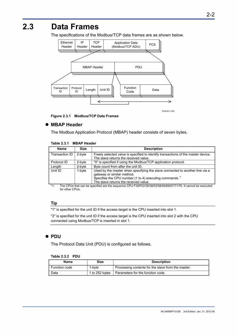
2.3 Data Frames The specifications of the Modbus/TCP data frames are as shown below.
F020301.VSD
Ethernet Header
IP Header
TCP Header
Application Data(Modbus/TCP ADU) FCS
MBAP Header PDU
TransactionID
Protocol ID Length Unit ID Function
Code Data
Figure 2.3.1 Modbus/TCP Data Frames
MBAP Header The Modbus Application Protocol (MBAP) header consists of seven bytes.
Table 2.3.1 MBAP Header Name Size Description
Transaction ID 2-byte Freely selected value is specified to identify transactions of the master device. The slave returns the received value.
Protocol ID 2-byte "0" is specified if using the Modbus/TCP application protocol. Length 2-byte Byte count from after the unit ID. Unit ID 1-byte Used by the master when specifying the slave connected to another line via a
gateway or similar method. Specifies the CPU number (1 to 4) executing commands.*1 The slave returns the received value.
*1: The CPUs that can be specified are the sequence CPU F3SP22/28/38/53/58/59/66/67/71/76. It cannot be executed for other CPUs.
Tip "1" is specified for the unit ID if the access target is the CPU inserted into slot 1.
"2" is specified for the unit ID if the access target is the CPU inserted into slot 2 with the CPU connected using Modbus/TCP is inserted in slot 1.
PDU The Protocol Data Unit (PDU) is configured as follows. Table 2.3.2 PDU
Name Size Description Function code 1-byte Processing contents for the slave from the master. Data 1 to 252 bytes Parameters for the function code.

2-3
IM 34M06P15-03E 2nd Edition: Jan. 31, 2012-00
2.4 Function Codes This section describes the Modbus function codes.
Support Function Codes The functions codes supported by this module are as shown below. Table 2.4.1 Function Code List
Function Code
Name Description Supported
01 ($01) Read Coils Consecutively reads the status of a max. of 2,000 coils.
Yes
02 ($02) Read Discrete Inputs Consecutively reads the status of a max. of 2,000 inputs.
Yes
03 ($03) Read Holding Registers Consecutively reads the status of a max. of 125 holding registers.
Yes
04 ($04) Read Input Registers Consecutively reads the status of a max. of 125 input registers.
Yes
05 ($05) Write Single Coil Writes a single coil. Yes 06 ($06) Write Single Register Writes a single register. Yes 15 ($0F) Write Multiple Coils Consecutively writes the status of a max. of
1,968 coils. Yes
16 ($10) Write Multiple Registers Consecutively writes the status of a max. of 123 registers.
Yes
20 ($14) Read File Record Reads a max. of 124 file records. Yes 21 ($15) Write File Record Writes a max. of 122 file records. Yes 22 ($16) Mask Write Register Mask a single register with AND or OR. Yes 23 ($17) Read/Write Multiple Registers Reads and writes multiple registers. Yes 24 ($18) Read FIFO Queue Reads FIFO tables. Yes

2-4
IM 34M06P15-03E 2nd Edition: Jan. 31, 2012-00
PDU Configuration This subsection describes the configuration of function codes and data.
Specifying Device Numbers in PDU "(Device number) - 1" is specified in the PDU for setting a device number. The above does not apply to file and record numbers specified at Read/Write File Record command.
F020401.VSD
Example: If the status of holding register no. 32 is single-word read at Read Holding Registers ($03).
Function Code Data
$03Starting Holding Register No.
$001FRead Points
$0001
31 ($001F) is specified as the starting address of the holding register for reading holding register no.32.
Figure 2.4.1 Specifying Device Numbers
Device numbers stored in responses are request command device numbers.
Tip $0000 is used in the PDU for specifying the starting coil number 00001 corresponding to I0001.
How to Read the Format This subsection explains how to read the request/response format block diagram.
F020402.VSD
Function Code Data
$01
1-byte 2-byte 2-byte
Starting Coil Nos.($0000 to $FFFF)
Read Points($0001 to $07D0)
Area NameFrame Contents Settings/Storage Range
Area Size
Figure 2.4.2 How to Read Format

2-5
IM 34M06P15-03E 2nd Edition: Jan. 31, 2012-00
2.5 Response Error Code This section describes the response error codes.
If Error Response is Returned This module returns a response as shown below if there is a mismatch in the PDU during a request or an error during processing.
F020501.VSD
(PDU at Faulty Completion)
Function Code Data
XX
1-byte
Error Code
1-byte
Figure 2.5.1 PDU at Faulty Completion
The request function code +$80 value is inserted in the function code (XX).
Response Error Code Table 2.5.1 Response Error Code
Error Code Meaning Cause $01 Function Code Error There is no function code. $02 Address Error Out-of-range address was specified. $03 Amount Error Out-of-range amount was specified. $04 Processing Error Write protect is specified. $0A CPU Number Error Unit ID that is not from 1 to 4 was specified. $0B Timeout CPU specified by the unit ID does not exist.

2-6
IM 34M06P15-03E 2nd Edition: Jan. 31, 2012-00
2.6 Modbus Device Allocation Specifications This section describes the associations between the Modbus device and the devices of this module.
Modbus Device List Modbus devices are as defined below. Devices are as described below. Table 2.6.1 Modbus Device List
Modbus Device Unit/Direction Points Number Coil 1-bit/Read, Write 65,536 1 to 65536 Discrete input 1-bit/Read 65,536 1 to 65536 Input register 16-bit/Read 65,536 1 to 65536 Holding register 16-bit/Read, Write 65,536 1 to 65536 File record 16-bit/Read, Write 655,360,000 File: 0 to 65535
Record: 0 to 9999
2-7
IM 34M06P15-03E 2nd Edition: Jan. 31, 2012-00
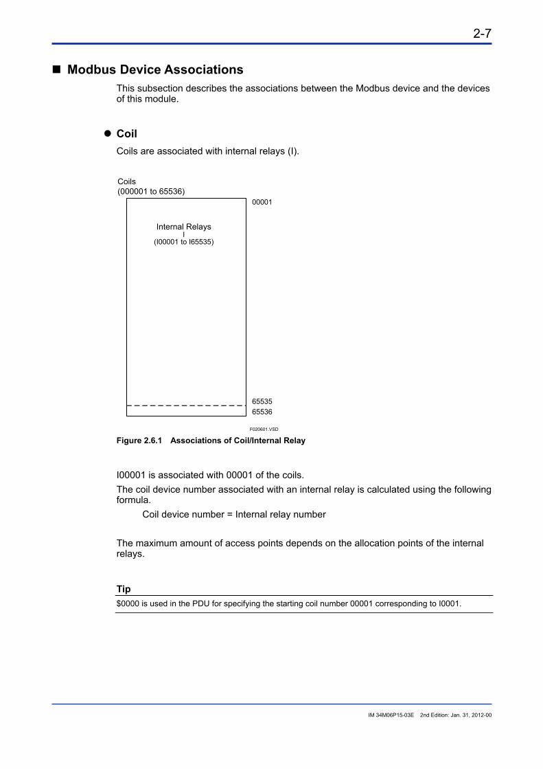
Modbus Device Associations This subsection describes the associations between the Modbus device and the devices of this module.
Coil Coils are associated with internal relays (I). Coils(000001 to 65536)
F020601.VSD
Internal RelaysI
(I00001 to I65535)
6553565536
00001
Figure 2.6.1 Associations of Coil/Internal Relay
I00001 is associated with 00001 of the coils. The coil device number associated with an internal relay is calculated using the following formula.
Coil device number = Internal relay number The maximum amount of access points depends on the allocation points of the internal relays.
Tip $0000 is used in the PDU for specifying the starting coil number 00001 corresponding to I0001.

2-8
IM 34M06P15-03E 2nd Edition: Jan. 31, 2012-00
Discrete Inputs Discrete inputs are associated with input relays (X) and special relays (M). Discrete Inputs(00001 to 65536)
F020602.VSD
Input RelaysX
(X00201 to X71664)
19984
65536
00001
00064
Special RelaysM
(M00001 to M09984)
00065
0819208193
1000010001
19985
Figure 2.6.2 Associations of Discrete Inputs with Internal Relays (X) and Special Relays (M)
X00201 is associated with input 00065. The input device number associated with an input relay is calculated using the following formula.
Input device number = Unit number x 1024 + (Slot number - 1) x 64 + Terminal number
M00001 is associated with input 10001. The input device number associated with a special relay is calculated using the following formula.
Input device number = Special relay number + 10000
Tip $0040 is used in the PDU for specifying the input number 00065 corresponding to X00201.
$2710 is used in the PDU for specifying the input number 10001 corresponding to M0001.

2-9
IM 34M06P15-03E 2nd Edition: Jan. 31, 2012-00
Input Register Special registers (Z) are associated with input registers. Input Registers(00001 to 65536)
F020603.VSD
Special RegistersZ
(Z00001 to Z01024)
01024
65536
00001
01025
Figure 2.6.3 Associations of Input Registers with Special Registers (Z)
Z00001 is associated with 00001 of the input registers. The input register device number associated with a special register is calculated using the following formula.
Input register device number = Special register number
Tip $0000 is used in the PDU for specifying the input register number 00001 corresponding to Z00001.
2-10
IM 34M06P15-03E 2nd Edition: Jan. 31, 2012-00
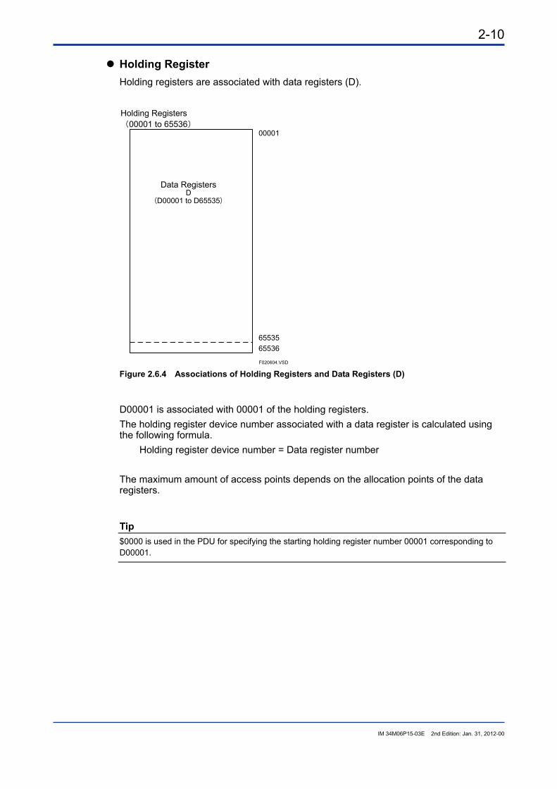
Holding Register Holding registers are associated with data registers (D). Holding Registers(00001 to 65536)
F020604.VSD
Data RegistersD
(D00001 to D65535)
65536
00001
65535
Figure 2.6.4 Associations of Holding Registers and Data Registers (D)
D00001 is associated with 00001 of the holding registers. The holding register device number associated with a data register is calculated using the following formula.
Holding register device number = Data register number The maximum amount of access points depends on the allocation points of the data registers.
Tip $0000 is used in the PDU for specifying the starting holding register number 00001 corresponding to D00001.

2-11
IM 34M06P15-03E 2nd Edition: Jan. 31, 2012-00
File Record File records are associated with file registers (B) and cache registers (F). File Records(File Nos. 00000 to 65535)(Record Nos. 0000 to 9999)
F020605.VSD
File RegistersB
(B000001 to B262144)
0000File Nos.
09999
File Nos.1
· · ·
0000
9999
File Nos.26
· · ·
File Nos.100
File Nos.101
· · ·
File Nos.152
· · ·
File Nos.65535
0000
9999
0000
99990000
9999
0000
9999
0000
9999
Cache RegistersF
(F000001 to F524288)
Figure 2.6.5 Associations of File Records
B00001 is associated with record number 0000 of file number 0. The file and record numbers associated with file registers are calculated using the following formula.
File number = File register number / 10000 Record number = File register number % 10000 - 1
The maximum amount of access points depends on the allocation points of the file registers. F00001 is connected with record code number 0000 of file number 100. The file and record numbers associated with cache registers are calculated using the following formula.
File number = Cache register number / 10000 + 100 File number = Cache register number % 10000 - 1
The maximum amount of access points depends on the allocation points of the file registers.
2-12
IM 34M06P15-03E 2nd Edition: Jan. 31, 2012-00
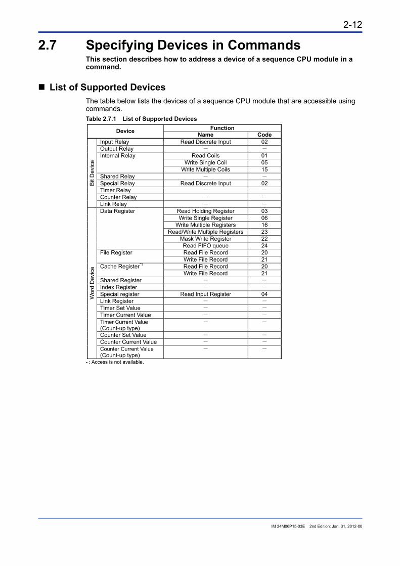
2.7 Specifying Devices in Commands This section describes how to address a device of a sequence CPU module in a command.
List of Supported Devices The table below lists the devices of a sequence CPU module that are accessible using commands. Table 2.7.1 List of Supported Devices
Function Device Name Code Input Relay Read Discrete Input 02 Output Relay - -
Read Coils 01 Write Single Coil 05
Internal Relay
Write Multiple Coils 15 Shared Relay - - Special Relay Read Discrete Input 02 Timer Relay - - Counter Relay - -
Bit
Dev
ice
Link Relay - - Read Holding Register 03 Write Single Register 06
Write Multiple Registers 16 Read/Write Multiple Registers 23
Mask Write Register 22
Data Register
Read FIFO queue 24 Read File Record 20 File Register Write File Record 21 Read File Record 20 Cache Register*1 Write File Record 21
Shared Register - - Index Register - - Special register Read Input Register 04 Link Register - - Timer Set Value - - Timer Current Value - - Timer Current Value (Count-up type)
- -
Counter Set Value - - Counter Current Value - -
Wor
d D
evic
e
Counter Current Value (Count-up type)
- -
- : Access is not available.

2-13
IM 34M06P15-03E 2nd Edition: Jan. 31, 2012-00
2.8 Modbus/TCP Slave Function Settings This section describes the settings for using the Modbus/TCP slave function.
Required Settings Settings required for using the Modbus/TCP slave function via Ethernet are as shown below. Table 2.8.1 Required Settings (Modbus/TCP Slave Function via Ethernet)
Setting Name Setting Type Reference for Details*1 Ethernet Settings CPU Properties A9.5.2 Ethernet Setup Higher-Level Link Service Settings
CPU Properties A9.5.4 Higher-level Link Service Setup
*1: Refer to items of "Sequence CPU Instruction Manual - Functions (for F3SP71-4N/4S, F3SP76-7N/7S)" (IM 34M06P15-01E).
Ethernet Settings Settings are specified in order to connect to an Ethernet network. At a minimum, IP address and subnet mask settings are required. If 0.0.0.0 is specified for the subnet mask, a default mask corresponding to the IP address class is used.
Higher-Level Link Service Settings Specify "2" for the port A or B protocol setting in order to use the Modbus/TCP slave function. At this time, that port executes the Modbus/TCP slave function at port number 502 and the value of the command data format is ignored. Additionally, enable the write-protect function (writing not permitted) if you want to prohibit device writing using the Modbus/TCP slave function. Table 2.8.2 Higher-Level Link Service Settings
Setting Description Setting Range Initial Value Higher-Level Link Service: Port A Protocol
For selecting the protocol used by port A of the higher-level link service of the Ethernet route. Port number of port A is 12289 ($3001) if TCP/IP or UDP/IP is selected, and port number is 502 ($1F6) if Modbus/TCP (slave) is selected.
0 = TCP/IP 1 = UDP/IP 2 = Modbus/TCP (Slave)
0 (TCP/IP)
Higher-Level Link Service: Port A Command Data Format
For selecting the command data format used by port A of the higher-level link service of the Ethernet route. Ignored if Modbus/TCP (slave).
0 = ASCII format 1 = Binary format
0 (ASCII format)
Higher-Level Link Service: Port B Protocol
For selecting the protocol used by port B of the higher-level link service of the Ethernet route. Port number of port B is 12291 ($3003) if TCP/IP or UDP/IP is selected, and port number is 502 ($1F6) if Modbus/TCP (slave) is selected.
0 = TCP/IP 1 = UDP/IP 2 = Modbus/TCP (Slave)
0 (TCP/IP)
Higher-Level Link Service: Port B Command Data Format
For selecting the command data format used by port B of the higher-level link service of the Ethernet route. Ignored if Modbus/TCP (slave).
0 = ASCII format 1 = Binary format
1 (Binary format)
Write Protect Setting to prohibit writing command to this module by the higher-level link service of the Ethernet route.
0 = Writing permitted 1 = Writing not permitted
0 (Writing permitted)

2-14
IM 34M06P15-03E 2nd Edition: Jan. 31, 2012-00
Settings Specified as Necessary Settings specified as necessary for using the Modbus/TCP slave function via Ethernet are as shown below. Table 2.8.3 Settings Specified as Necessary (Modbus/TCP Slave Function via Ethernet)
Setting Name Setting Type Reference for Details*1 Network Filter Settings CPU Properties A9.5.8 Network Filter Setup CPU Operation Restriction
Operation Protection Settings
A.6.22.8 CPU Operation Restriction
*1: Refer to items of "Sequence CPU Instruction Manual - Functions (for F3SP71-4N/4S, F3SP76-7N/7S)" (IM 34M06P15-01E).
Network Filter Settings This setting restricts the IP addresses allowed to access this module. The initial value permits all IP addresses to access this module. This setting is referenced from all functions that correspond to higher-level link service functions via Ethernet, such as remote programming service and FTP server.
CPU Operation Restriction Use this setting if you want to protect higher-level link services. CPU operation restriction can be used to protect operating mode switching, log acquisition and other CPU operations that do not use WideField3, depending on the combination of various access routes and CPU operation permission groups.
SEE ALSO For the CPU operation restriction function (operation protection), refer to "A6.22.8 CPU Operation Restriction" of “Sequence CPU Instruction Manual - Functions (for F3SP71-4N/4S,F3SP76-7N/7S)” (IM 34M06P15-01E).
2-15
IM 34M06P15-03E 2nd Edition: Jan. 31, 2012-00
2.9 Using Modbus/TCP Slave Function via Ethernet This section describes how to use the Modbus/TCP slave function via Ethernet.
Connecting to a Monitor To connect to a monitor, perform the following steps: 1. Create screen data on a PC. 2. Transfer screen data to a monitor. 3. Match the communication setup of the monitor and the module. 4. Connect the monitor and the module. Begin monitoring.
SEE ALSO For details on how to connect to the monitor, see the documentation of the monitor.
Connecting to a PC Connecting to a Program Created on a PC To connect to a program on a PC, perform the following steps: 1. Create a communication program on a PC (using Visual Basic, etc.) 2. Match the communication setup of the communication program and the module. 3. Connect the communication program and the module. Begin monitoring.
Connecting to a SCADA Application To connect to a SCADA application on a PC, perform the following steps: 1. Create screen data on a PC. 2. Match the communication setup of SCADA and the module. 3. Connect SCADA and the module. Begin monitoring.
SEE ALSO For details on the application (Visual BASIC or SCADA) on the PC end, see the documentation for the application.
2.

Blank Page

3-1
IM 34M06P15-03E 2nd Edition: Jan. 31, 2012-00
3. Command/Response Details
3.1 Read Coils ($01) Reads the status (on/off) of a single or multiple coils. The amount of devices that can be accessed with a single request is 1 to 2,000 points.
Request Format (Master => Slave)
F030101.VSD
Function Code Data
$01
1-byte 2-byte 2-byte
Starting Coil Nos.($0000 to $FFFF)
Read Points($0001 to $07D0)
Response Format (Slave => Master)
(At Normal Completion)
Function Code Data
$01
1-byte
Read Length n
($01 to $FA)1-byte 1-byte
Device Data1
Device Datan
1-byte
・・・
(At Faulty Completion)
Function Code Data
$81
1-byte
Error Code
1-byte
・・・
Bit Device Storage Order
- Stored from lower => higher-level bit order.- Remainder bits are made "0".
bit7 bit6 bit5 bit4 bit3 bit2 bit1 bit0
Device Data 1
Device Data n
0 : OFF1 : ON

3-2
IM 34M06P15-03E 2nd Edition: Jan. 31, 2012-00
3.2 Read Discrete Inputs ($02) Reads the status (on/off) of a single or multiple inputs. The amount of devices that can be accessed with a single request is 1 to 2,000 points.
Request Format (Master => Slave)
F030102.VSD
Function Code Data
$02
1-byte 2-byte 2-byte
Starting Input Nos.($0000 to $FFFF)
Read Points($0001 to $07D0)
Response Format (Slave => Master)(At Normal Completion)
Function Code Data
$02
1-byte
Read Length n
($01 to $FA)1-byte 1-byte
Device Data1
Device Datan
1-byte
···
(At Faulty Completion)
Function Code Data
$82
1-byte
Error Code
1-byte
・・・
Bit Device Storage Order
- Stored from lower => higher-level bit order.- Remainder bits are made "0".
bit7 bit6 bit5 bit4 bit3 bit2 bit1 bit0
Device Data
Device Data n
0 : OFF1 : ON

3-3
IM 34M06P15-03E 2nd Edition: Jan. 31, 2012-00
3.3 Read Holding Registers ($03) Reads the value(s) of a single or multiple holding registers. The amount of devices that can be accessed with a single request is 1 to 125 points. Request Format (Master => Slave)
F030103.VSD
Function Code Data
$03
1-byte 2-byte 2-byte
Starting Holding Register Nos.($0000 to $FFFF)
Read Points($0001 to $007D)
Response Format (Slave => Master)
(At Normal Completion)
Function Code Data
$03
1-byte
Read Length nx2
($02 to $FA)1-byte 2-byte
Device Data1
Device Datan
2-byte
···
(At Faulty Completion)
Function Code Data
$83
1-byte
Error Code
1-byte

3-4
IM 34M06P15-03E 2nd Edition: Jan. 31, 2012-00
3.4 Read Input Registers ($04) Reads the value(s) of a single or multiple input registers. The amount of devices that can be accessed with a single request is 1 to 125 points. Request Format (Master => Slave)
F030104.VSD
Function Code Data
$04
1-byte 2-byte 2-byte
Starting Input Register Nos.($0000 to $FFFF)
Read Points($0001 to $007D)
Response Format (Slave => Master)
(At Normal Completion)
Function Code Data
$04
1-byte
Read Length nx2
($02 to $FA)1-byte 2-byte
Device Data1
Device Datan
2-byte
・・・
(At Faulty Completion)
Function Code Data
$84
1-byte
Error Code
1-byte

3-5
IM 34M06P15-03E 2nd Edition: Jan. 31, 2012-00
3.5 Write Single Coil ($05) Writes the value (either 1 or 0) to a single coil. The amount of devices that can be accessed with a single request is one point. Request Format (Master => Slave)
F030105.VSD
Function Code Data
$05
1-byte 2-byte 2-byte
Coil Nos.($0000 to $FFFF)
Specified Value1:$FF000:$0000
Response Format (Slave => Master)
(At Normal Completion)
(At Faulty Completion)
Function Code Data
$85
1-byte
Error Code
1-byte
Function Code Data
$05
1-byte 2-byte 2-byte
Coil Nos.(Same Value as Request)
Specified Value(Same Value as Request)
The slave returns the request received from the master with no change.

3-6
IM 34M06P15-03E 2nd Edition: Jan. 31, 2012-00
3.6 Write Single Register ($06) Writes the value to a single holding register. The amount of devices that can be accessed with a single request is one point. Request Format (Master => Slave)
F030106.VSD
Function Code Data
$06
1-byte 2-byte 2-byte
Holding Register Nos.($0000 to $FFFF)
Write Points($0000 to $FFFF)
Response Format (Slave => Master)
(At Normal Completion)
(At Faulty Completion)
Function Code Data
$86
1-byte
Error Code
1-byte
Function Code Data
$06
1-byte 2-byte 2-byte
Holding Register Nos.(Same Value as Request)
Write Points(Same Value as Request)
The slave returns the request received from the master with no change.

3-7
IM 34M06P15-03E 2nd Edition: Jan. 31, 2012-00
3.7 Write Multiple Coils ($0F) Writes the value (either 1 or 0) to multiple coils. The amount of devices that can be accessed with a single request is 1,968 points. Request Format (Master => Slave)
Response Format (Slave => Master)
(At Normal Completion)
F030107.VSD
・・・
Bit Device Storage Order
- Stored in coil from lower => higher-level bit order.
bit7 bit6 bit5 bit4 bit3 bit2 bit1 bit0
Device Data 1
Device Data n
0 : OFF1 : ON
Function Code Data
$0F
1-byte
Starting Coil Nos.($0000 to $FFFF)
Write Points($0001 to $07B0)
Write Length n
($01 to $F6)
Device Data
Device Data
n・・・
2-byte 2-byte 1-byte 1-byte 1-byte
Function Code Data
$0F
1-byte
Data
$8F
1-byte 1-byte
Error Code
Function Code
Starting Coil Nos.(Same Value as Request)
Write Points(Same Value as Request)
2-byte2-byte
(At Faulty Completion)
Writing is performed by dividing into multiple scans if the write points are 16 m (multiples of 16).

3-8
IM 34M06P15-03E 2nd Edition: Jan. 31, 2012-00
3.8 Write Multiple Registers ($10) Writes the values to multiple holding registers. The amount of devices that can be accessed with a single request is 1 to 123 points.
Request Format (Master => Slave)
F030108.VSD
Function Code Data
$10
1-byte 2-byte 2-byte
Starting Holding Register Nos.($0000 to $FFFF)
Write Points($0001 to $007B)
Response Format (Slave => Master)
(At Normal Completion)
(At Faulty Completion)
Function Code Data
$90
1-byte
Error Code
1-byte
Function Code Data
$10
1-byte 2-byte 2-byte
Starting Holding Register Nos.(Same Value as Request)
Write Points(Same Value as Request)
Data
Write Length nx2
($02 to $F6)1-byte 2-byte
Device Data1
Device Datan
2-byte
・・・

3-9
IM 34M06P15-03E 2nd Edition: Jan. 31, 2012-00
3.9 Read File Record ($14) Reads the values of multiple file records. The amount of devices that can be accessed with a single request is 1 to 124 points.
Request Format (Master => Slave)
F030109.VSD
Function Code Data
$14
1-byte 1-byte
Length(7×m)
Data
Reference No.$06
1-byte 2-byte
File Nos.($0000 to $FFFF)
Read Starting Record Nos.
($0000 to $270F)2-byte
Sub-request 1
2-byte
Read Record Count($0000 to $007C)
n1
Data
Reference No.$06
1-byte 2-byte
File Nos.($0000 to $FFFF)
Read Starting Record Nos.
($0000 to $270F)2-byte
Sub-request m
2-byte
Read Record Count($0000 to $007C)
nm
(a) Specify the sub-request count m so that the request PDU (protocol data units) size does not exceed 253 bytes (m ≤ 35).
(b) Specify the total read points N (n1 + ... + nm) of each sub-request so
that the response PDU (protocol data units) size does not exceed 253 bytes.

3-10
IM 34M06P15-03E 2nd Edition: Jan. 31, 2012-00
F030110.VSD
Response Format (Slave => Master)
(At Normal Completion)
(At Faulty Completion)
Function Code Data
$14
1-byte 1-byte
Length
Data
Reference No.$06
1-byte 2-byte
Sub-request 1
2-byte1-byte
Read Data Sizen1 × 2 + 1
Data 1 Data n1・・・
Data
Reference No.$06
1-byte 2-byte
Sub-request m
2-byte1-byte
Read Data Sizenm × 2 + 1
Data 1 Data nm・・・
Data
$94
1-byte 1-byte
Error Code
Function Code

3-11
IM 34M06P15-03E 2nd Edition: Jan. 31, 2012-00
3.10 Write File Record ($15) Writes the values to multiple file records. The amount of devices that can be accessed with a single request is 1 to 122 points.
F030111.VSD
Function Code Data
$15
1-byte 1-byte
Length
Data
Reference No.$06
1-byte 2-byte
File Nos.($0000 to $FFFF)
Write Starting Record Nos.
($0000 to $270F)2-byte
Sub-request 1
2-byte
Write Record Count($0000 to $007A)
n1Data 1 Data n1
2-byte 2-byte
Request Format (Master => Slave)
Data
Reference No.$06
1-byte 2-byte
File Nos.($0000 to $FFFF)
Write Starting Record Nos.
($0000 to $270F)2-byte
Sub-request m
2-byte
Write Record Count($0000 to $007A)
nmData 1 Data nm
2-byte 2-byte
(a) Specify the total read points N (n1 + ... + nm) of each sub-request so
that the response PDU (protocol data units) size does not exceed 253 bytes.
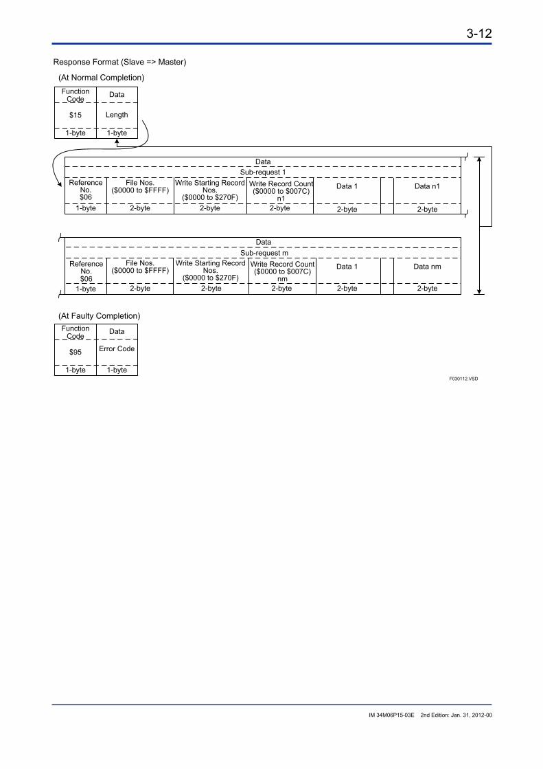
3-12
F030112.VSD
Response Format (Slave => Master)
(At Normal Completion)
(At Faulty Completion)
Data
$95
1-byte 1-byte
Error Code
Function Code
Function Code Data
$15
1-byte 1-byte
Length
Data
Reference No.$06
1-byte 2-byte
File Nos.($0000 to $FFFF)
Write Starting Record Nos.
($0000 to $270F)2-byte
Sub-request 1
2-byte
Write Record Count($0000 to $007C)
n1
Data 1 Data n1
2-byte 2-byte
Data
Reference No.$06
1-byte 2-byte
File Nos.($0000 to $FFFF)
Write Starting Record Nos.
($0000 to $270F)2-byte
Sub-request m
2-byte
Write Record Count($0000 to $007C)
nm
Data 1 Data nm
2-byte 2-byte
IM 34M06P15-03E 2nd Edition: Jan. 31, 2012-00

3-13
IM 34M06P15-03E 2nd Edition: Jan. 31, 2012-00
3.11 Mask Write Register ($16) Masks the value stored in a single holding register using AND or OR, and writes the value. The amount of devices that can be accessed with a single request is one point. The value written into a holding register is as described below.
Written value = (Current value & AND mask value) | (OR mask value & ~AND mask value)
If the OR mask value is $0000, only AND processing of the AND mask value is performed. If the AND mask value is $0000, the OR mask value is the written value.
Response Format (Slave => Master)
F030113.VSD
Function Code Data
$16
1-byte 2-byte 2-byte
Starting Register Nos.($0000 to $FFFF)
AND Mask Value($0000 to $FFFF)
Response Format (Master => Slave )
(At Normal Completion)
(At Faulty Completion)
Function Code Data
$96
1-byte
Error Code
1-byte
OR Mask Value($0000 to $FFFF)
2-byte
Function Code Data
$16
1-byte 2-byte 2-byte
Starting Register Nos.($0000 to $FFFF)
AND Mask Value($0000 to $FFFF)
OR Mask Value($0000 to $FFFF)
2-byte
Tip This function reads the value stored in the holding register from the slave, performs AND/OR processing, and then writes the value in the storage register. Accordingly, if the holding register value changes during AND/OR processing, the changed value is overwritten.

3-14
IM 34M06P15-03E 2nd Edition: Jan. 31, 2012-00
3.12 Read/Write Multiple Registers ($17) Reads and writes multiple holding registers. Processing consists of writing followed by reading. The amount of devices that can be accessed with a single request is 1 to 125 points for reading and 1 to 121 points for writing.
Request Format (Master => Slave)
F030114.VSD
Function Code Data
$17
1-byte 2-byte 2-byte
Read Starting Holding Register Nos.
($0000 to $FFFF)
Read Points($0001 to $007D)
n
Response Format (Slave => Master)
(At Normal Completion)
(At Faulty Completion)
Data
$97
1-byte
Error Code
1-byte
Data
$17
1-byte 2-byte 2-byte
Device Data1
Device Datan
Data
Write Length m×2
2-byte
Write Starting Holding Register Nos.
($0000 to $FFFF)1-byte 2-byte
Device Data1
Device Datam
2-byte
・・・
2-byte
Write Points($0001 to $0079)
m
Function Code
1-byte
Read Length
n×2
Function Code
Writing and reading processes are performed using separate scans.

3-15
IM 34M06P15-03E 2nd Edition: Jan. 31, 2012-00
3.13 Read FIFO Queue ($18) Reads the value(s) of a single or multiple holding registers. The amount of devices that can be accessed with a single request is 1 to 31 points.
Request Format (Master => Slave)
F030115.VSD
Function Code Data
$18
1-byte 2-byte
FIFO Pointer Nos.($0000 to $FFFF)
Response Format (Slave => Master)
(At Normal Completion)
(At Faulty Completion)
Data
$98
1-byte
Error Code
1-byte
Data
2-byte 2-byte
Device Data1
Device Datan
2-byte
・・・
2-byte
FIFO Count($0000 to $001F)
Function Code
Length($0002 to $0040)
Function Code
$18
1-byte
3.

Blank Page

i
IM 34M06P15-03E 2nd Edition: Jan. 31, 2012-00
Revision Information Document Name: Sequence CPU - Modbus/TCP Functions Document No. : IM 34M06P15-03E
Edition Date Revised Item
1st June 2011 New publication 2nd Jan. 2012 Errata
Written by PLC Group International Sales Promotion Dept. IA Systems Business Headquarters Yokogawa Electric Corporation Published by Yokogawa Electric Corporation 2-9-32 Nakacho, Musashino-shi, Tokyo, 180-8750, JAPAN Printed by Kohoku Publishing & Printing Inc.

Blank Page