extending arfi immersion scanner capability in support of ... · frank bornebroek . feb 27. th....
TRANSCRIPT

Frank Bornebroek Feb 27th 2014, SPIE Advanced Lithography, San Jose
Extending ArFi immersion scanner capability in support of 1xnm production nodes

Contents
• Lithography requirements & immersion roadmap
• New ArFi technology introduced in HVM • Productivity • Focus control • Imaging • Overlay
• Future developments & Summary
5 March 2014
Public Slide 2
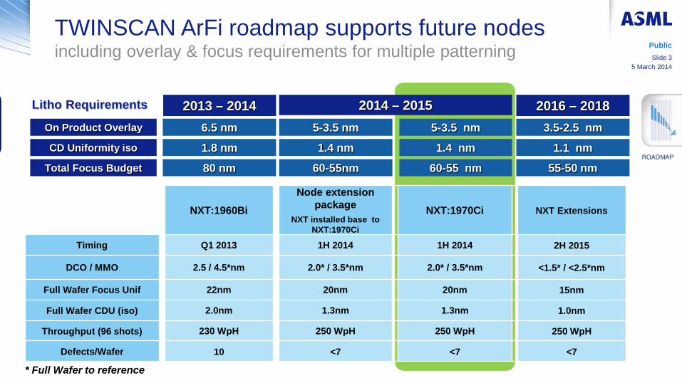
TWINSCAN ArFi roadmap supports future nodes including overlay & focus requirements for multiple patterning
NXT:1960Bi
Node extension package
NXT installed base to NXT:1970Ci
NXT:1970Ci NXT Extensions
Timing Q1 2013 1H 2014 1H 2014 2H 2015
DCO / MMO 2.5 / 4.5*nm 2.0* / 3.5*nm 2.0* / 3.5*nm <1.5* / <2.5*nm
Full Wafer Focus Unif 22nm 20nm 20nm 15nm
Full Wafer CDU (iso) 2.0nm 1.3nm 1.3nm 1.0nm
Throughput (96 shots) 230 WpH 250 WpH 250 WpH 250 WpH
Defects/Wafer 10 <7 <7 <7
On Product Overlay 6.5 nm 5-3.5 nm
CD Uniformity iso 1.8 nm 1.4 nm
Total Focus Budget 80 nm 60-55 nm
2013 – 2014 2014 – 2015 Litho Requirements
3.5-2.5 nm
1.1 nm
55-50 nm
2016 – 2018
* Full Wafer to reference
5-3.5 nm
1.4 nm
60-55nm
5 March 2014
Public Slide 3

0
1000
2000
3000
4000
5000
6000
Foundry DRAM NAND
Wafers per Day (actuals)
Best week
Best quarter
NXT:1960Bi systems show high productivity Up to > 4000 WpD quarter average, > 5000 WpD best week average
NXT: 1960Bi installed base systems with utilization > 50%, max per segment
5 March 2014
Public Slide 4
65 systems (>50% utilization)
54 systems (>50% utilization)
39 systems (>50% utilization)

NXT:1970Ci is in use in HVM

Public
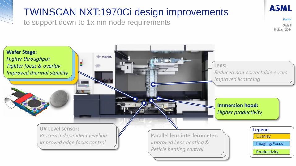
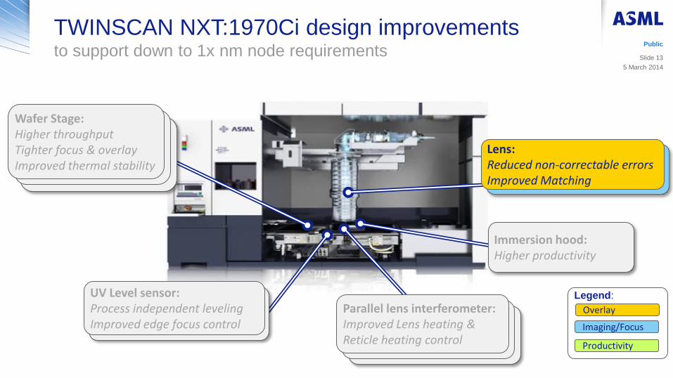
Overlay
Imaging/Focus
Productivity
Legend:
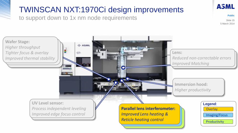
Lens: Reduced non-correctable errors Improved Matching
UV Level sensor: Process independent leveling Improved edge focus control
Parallel lens interferometer: Improved Lens heating & Reticle heating control
Wafer Stage: Higher throughput Tighter focus & overlay Improved thermal stability
Immersion hood: Higher productivity
5 March 2014 Slide 6
TWINSCAN NXT:1970Ci design improvements to support down to 10 nm node requirements
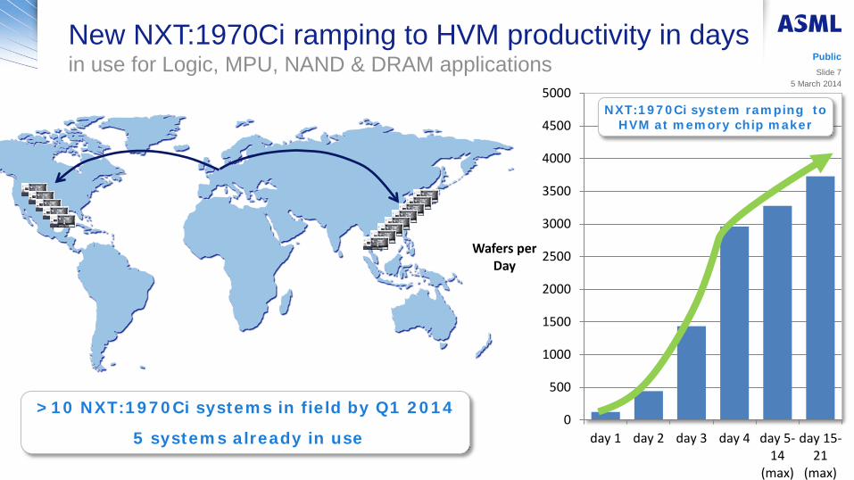
0
500
1000
1500
2000
2500
3000
3500
4000
4500
5000
day 1 day 2 day 3 day 4 day 5-14
(max)
day 15-21
(max)
Wafers per Day
New NXT:1970Ci ramping to HVM productivity in days in use for Logic, MPU, NAND & DRAM applications Public
>10 NXT:1970Ci systems in field by Q1 2014
5 systems already in use
NXT:1970Ci system ramping to HVM at memory chip maker
5 March 2014 Slide 7
Public
Overlay
Imaging/Focus
Productivity
Legend:
Lens: Reduced non-correctable errors Improved Matching
UV Level sensor: Process independent leveling Improved edge focus control
Parallel lens interferometer: Improved Lens heating & Reticle heating control
Wafer Stage: Higher throughput Tighter focus & overlay Improved thermal stability
5 March 2014 Slide 8
TWINSCAN NXT:1970Ci design improvements to support down to 1x nm node requirements
Immersion hood: Higher productivity
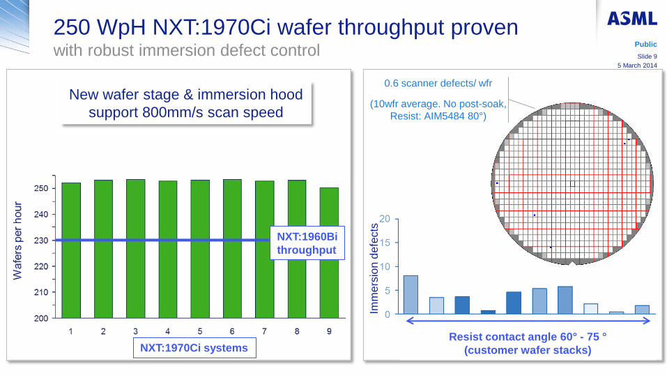
250 WpH NXT:1970Ci wafer throughput proven with robust immersion defect control
NXT:1960Bi throughput
New wafer stage & immersion hood support 800mm/s scan speed
0.6 scanner defects/ wfr
(10wfr average. No post-soak, Resist: AIM5484 80°)
Imm
ersi
on d
efec
ts
NXT:1970Ci systems
5 March 2014
Public Slide 9
Resist contact angle 60° - 75 ° (customer wafer stacks)
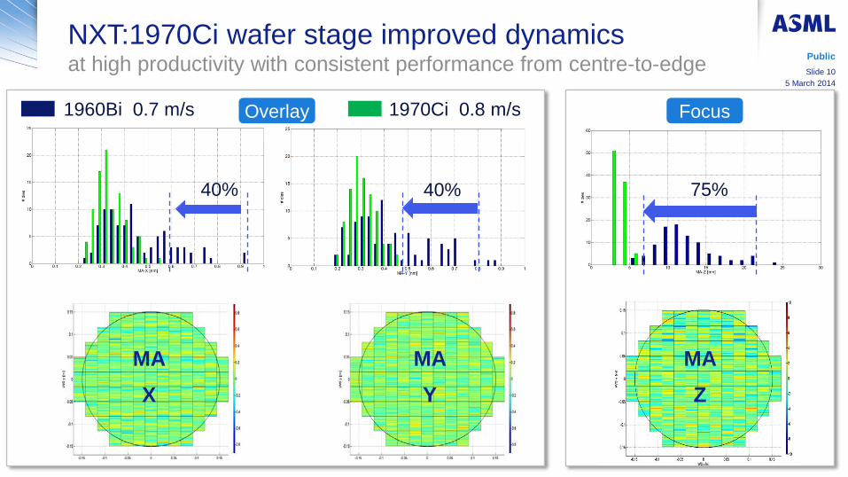
NXT:1970Ci wafer stage improved dynamics at high productivity with consistent performance from centre-to-edge
MA X
Overlay Focus 1970Ci 0.8 m/s 1960Bi 0.7 m/s
40% 75% 40%
5 March 2014
Public Slide 10
MA Y
MA Z
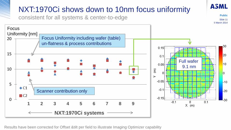
0
5
10
15
20
NXT:1970Ci shows down to 10nm focus uniformity consistent for all systems & center-to-edge
Results have been corrected for Offset &tilt per field to illustrate Imaging Optimizer capability
Full wafer 9.1 nm
Focus Uniformity [nm]
1 2 3 4 5 6 7 8
5 March 2014
Public Slide 11
Focus Uniformity including wafer (table) un-flatness & process contributions
Scanner contribution only
9
NXT:1970Ci systems
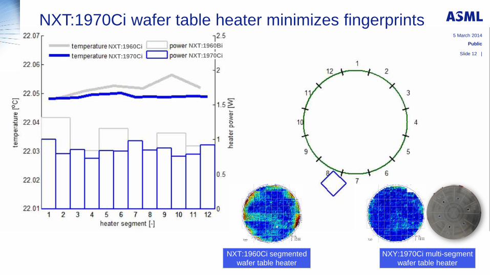
NXT:1970Ci wafer table heater minimizes fingerprints
NXT:1960Ci segmented wafer table heater
NXY:1970Ci multi-segment wafer table heater
NXT:1960Ci NXT:1960Bi NXT:1970Ci NXT:1970Ci
5 March 2014
Public
Slide 12 |
Overlay
Imaging/Focus
Productivity
Legend:
Lens: Reduced non-correctable errors Improved Matching
UV Level sensor: Process independent leveling Improved edge focus control
Parallel lens interferometer: Improved Lens heating & Reticle heating control
Wafer Stage: Higher throughput Tighter focus & overlay Improved thermal stability
Immersion hood: Higher productivity
TWINSCAN NXT:1970Ci design improvements to support down to 1x nm node requirements 5 March 2014
Public
Slide 13

Improved NXT:1970Ci projection lens aberration control proven at multiple systems
Pro
ject
ion
Lens
abe
rratio
ns [a
.u.]
RMS Z5-Z37
RMS Spherical
RMS Coma
RMS Astigmatism
RMS 3-Foil
NXT:1950i/60Bi (>200 systems)
NXT:1970Ci (7 systems)
5 March 2014
Public Slide 14
Overlay
Imaging/Focus
Productivity
Legend:
Lens: Reduced non-correctable errors Improved Matching
UV Level sensor: Process independent leveling Improved edge focus control
Parallel lens interferometer: Improved Lens heating & Reticle heating control
Wafer Stage: Higher throughput Tighter focus & overlay Improved thermal stability
TWINSCAN NXT:1970Ci design improvements to support down to 1x nm node requirements 5 March 2014
Public
Slide 15
Immersion hood: Higher productivity
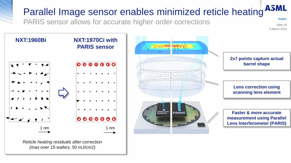
Parallel Image sensor enables minimized reticle heating PARIS sensor allows for accurate higher order corrections
2x7 points capture actual barrel shape
Faster & more accurate measurement using Parallel Lens Interferometer (PARIS)
Lens correction using scanning lens element
NXT:1960Bi NXT:1970Ci with PARIS sensor
Reticle heating residuals after correction (max over 15 wafers, 50 mJ/cm2)
5 March 2014
Public
Slide 16
1 nm 1 nm
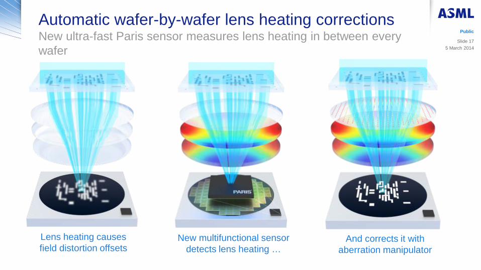
Automatic wafer-by-wafer lens heating corrections New ultra-fast Paris sensor measures lens heating in between every wafer
Lens heating causes field distortion offsets
New multifunctional sensor detects lens heating …
And corrects it with aberration manipulator
5 March 2014
Public
Slide 17

NXT:1970Ci lens heating corrections result in stable through-lot overlay
5 March 2014
Public
Slide 18
Lot-by-lot feed forward correction only
Wafer-by-wafer feed back correction with Paris sensor
wafers in lot wafers in lot
Overlay drift mainly due to low order aberration drift (Z2/3)
1st layer: Annular illumination | low reticle transmission 2nd layer: Dipole illumination | high reticle transmission
Machine Overlay
Machine Overlay

Overlay
Imaging/Focus
Productivity
Legend:
Lens: Reduced non-correctable errors Improved Matching
UV Level sensor: Process independent leveling Improved edge focus control
Parallel lens interferometer: Improved Lens heating & Reticle heating control
Wafer Stage: Higher throughput Tighter focus & overlay Improved thermal stability
TWINSCAN NXT:1970Ci design improvements to support down to 1x nm node requirements 5 March 2014
Public
Slide 19
Immersion hood: Higher productivity
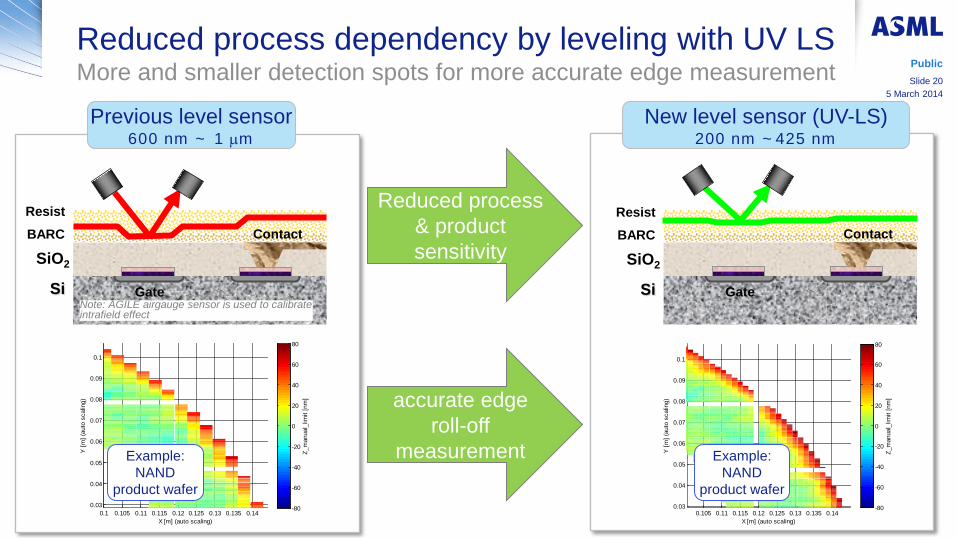
Gate
Contact
Si
SiO2 BARC Resist
Note: AGILE airgauge sensor is used to calibrate intrafield effect
Reduced process & product sensitivity
0.1 0.105 0.11 0.115 0.12 0.125 0.13 0.135 0.140.03
0.04
0.05
0.06
0.07
0.08
0.09
0.1
X [m] (auto scaling)
Y [m
] (au
to s
calin
g)
Z_m
anua
l_lim
it [n
m]
-80
-60
-40
-20
0
20
40
60
80
0.105 0.11 0.115 0.12 0.125 0.13 0.135 0.140.03
0.04
0.05
0.06
0.07
0.08
0.09
0.1
X [m] (auto scaling)
Y [m
] (au
to s
calin
g)
Z_m
anua
l_lim
it [n
m]
-80
-60
-40
-20
0
20
40
60
80
Gate
Contact
Si
SiO2 BARC Resist
accurate edge roll-off
measurement Example: NAND
product wafer
Example: NAND
product wafer
5 March 2014
Public Slide 20
Reduced process dependency by leveling with UV LS More and smaller detection spots for more accurate edge measurement
Previous level sensor 600 nm ~ 1 µm
New level sensor (UV-LS) 200 nm ~425 nm

NXT:1970Ci UV Level Sensor works for all applications
previous Level Sensor 600 nm ~ 1 µm
UV Level Sensor 200 nm ~ 425 nm
LOGIC DRAM NAND 5 March 2014
Public Slide 21
No air gauge sensor based intra-field fingerprint compensation applied

NXT:1970Ci system Imaging performance

NXT:1970Ci shows stable CDU through lot
40nm dense lines - full wafer
5 March 2014
Public Slide 23
Vertical Horizontal Vertical Horizontal
40nm isolated lines - full wafer
NXT:1970Ci system Overlay performance
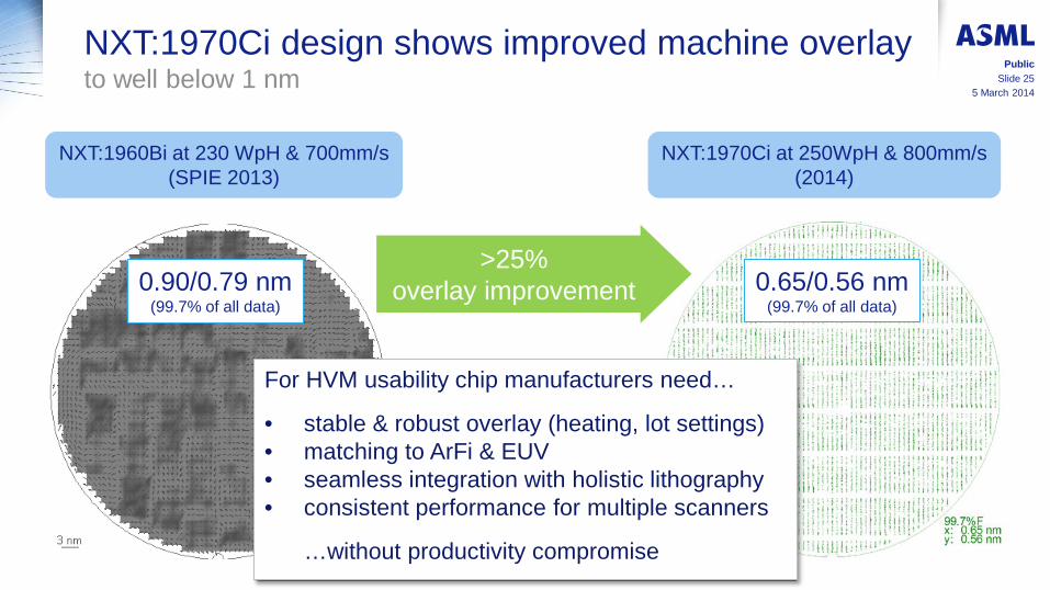
NXT:1970Ci design shows improved machine overlay to well below 1 nm
0.65/0.56 nm (99.7% of all data)
NXT:1960Bi at 230 WpH & 700mm/s (SPIE 2013)
NXT:1970Ci at 250WpH & 800mm/s (2014)
0.90/0.79 nm (99.7% of all data)
For HVM usability chip manufacturers need…
• stable & robust overlay (heating, lot settings) • matching to ArFi & EUV • seamless integration with holistic lithography • consistent performance for multiple scanners
…without productivity compromise
5 March 2014
Public Slide 25
>25% overlay improvement
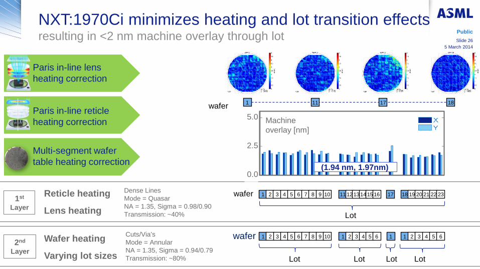
Dense Lines Mode = Quasar NA = 1.35, Sigma = 0.98/0.90 Transmission: ~40%
Cuts/Via’s Mode = Annular NA = 1.35, Sigma = 0.94/0.79 Transmission: ~80%
1 2 3 4 5 6 7 8 9 17 18 19 20 21 22 23 Chuck:
1 2 3 4 5 6 7 8 9 10 1 2 3 4 5 6 1 1 2 3 4 5 6
Reticle heating
Lens heating
Wafer heating
Varying lot sizes
NXT:1970Ci minimizes heating and lot transition effects resulting in <2 nm machine overlay through lot
5 March 2014
Public Slide 26
1st Layer
2nd Layer
Lot
Lot Lot Lot Lot
10 11 12 13 14 15 16
Paris in-line lens heating correction
Paris in-line reticle heating correction
Multi-segment wafer table heating correction
Machine overlay [nm]
1 17 18 11
(1.94 nm, 1.97nm)
wafer
wafer
wafer
5.0
2.5
0.0

NXT:1970Ci shows <2.5 nm matched overlay capability consistently for all systems
Results have been corrected for higher order wafer & field fingerprint NXT:1970Ci supports correction of higher order wafer & field fingerprints by holistic lithography
Matched machine overlay (ArFi to ArFi)
NXT:1970Ci systems
2.0 nm 1.9 nm
2.2 nm 1.9 nm
2.1 nm 2.0 nm
2.0 nm 2.0 nm
2.1 nm 1.9 nm
2.0 nm 2.0 nm
Wafers 1-6
5 March 2014
Public Slide 27

NXT:1970Ci ArFi supports EUV insertion overlay matching at 2.6nm demonstrated
YieldStar overlay metrology
2nd layer
NXT:1970Ci
1st layer
NXE:3300
Matched Overlay EUV to ArFi
X: 2.6 nm Y: 2.5 nm
5 March 2014
Public Slide 28

Future developments
Public Slide 29
5 March 2014

Future improvements will be driven by Overlay & Focus control Several improvement areas under investigation
Alignment improvements Improved robustness Improved accuracy
Wafer stage & wafer table Improved focus performance Improved temperature control
Reticle stage Further reticle heating improvements
Lens Improved temperature control Reduced non-correctable errors
Grid calibration improvements Reduction of grid calibration errors
5 March 2014
Public Slide 30

Summary
5 March 2014
Public Slide 31
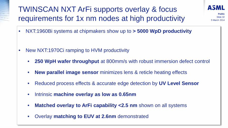
• NXT:1960Bi systems at chipmakers show up to > 5000 WpD productivity
• New NXT:1970Ci ramping to HVM productivity
• 250 WpH wafer throughput at 800mm/s with robust immersion defect control
• New parallel image sensor minimizes lens & reticle heating effects
• Reduced process effects & accurate edge detection by UV Level Sensor
• Intrinsic machine overlay as low as 0.65nm
• Matched overlay to ArFi capability <2.5 nm shown on all systems
• Overlay matching to EUV at 2.6nm demonstrated
TWINSCAN NXT ArFi supports overlay & focus requirements for 1x nm nodes at high productivity
5 March 2014
Public Slide 32

Acknowledgements to:
Janneke van Heteren, Joost Smits, Martijn Leenders, Igor Bouchoms, Wim de Boeij, Jan Jaap Kuit, Remi Pieternella, Toine de Kort, Peter Schrap, Jeroen Bominaar, Siebe Landheer, Mayke van der Ploeg, Alexander Padyi, Birgitt Hepp, Shufen Tsoi, Jeffry Goossens, Ron Schuurhuis, Richard Pongers, Pieter Gunter, Ruben Snijdewind, Mustafa Cem Unver, Paul Teunissen, Thomas Voss, Bart Smeets, Oksana Gnatiuk, Dion George, Afra de Graaf , Nico Vanroose, Marjan Hoofman, Roelof de Graaf, Haico Kok, Matthew McLaren