experimental and modeling studies on solder self …
TRANSCRIPT

EXPERIMENTAL AND MODELING STUDIES ON SOLDER SELF-ALIGNMENT
FOR OPTOELECTRONIC PACKAGING
by
MING KONG
B.S., Shanghai Jiao Tong University, 2003
M.S., University of Colorado at Boulder, 2010
A thesis submitted to the
Faculty of the Graduate School of the
University of Colorado in partial fulfillment
of the requirement for the degree of
Doctor of Philosophy
Department of Mechanical Engineering
2012

This dissertation entitled:
Experimental and Modeling Studies on Solder Self-alignment for Optoelectronic Packaging
written by Ming Kong
has been approved by the Department of Mechanical Engineering
Y.C. Lee
Victor M. Bright
Date______________
The final copy of this thesis has been examined by the signatories, and we
Find that both the content and the form meet acceptable presentation standards
Of scholarly work in the above mentioned discipline.

iii
Ming Kong (Ph.D., Mechanical Engineering, 2012)
Experimental and Modeling Studies on Solder Self-alignment for Optoelectronic
Packaging
Thesis directed by Professor Y.C. Lee
Abstract
Solder self-aligning technology is important to the manufacturing of cost-
effective optoelectronic modules requiring accurate alignments. This thesis is to
understand major effects on self-alignment accuracies in order to establish a model
to guide the design for precision solder self-alignments.
A solder self-alignment model based on force optimization with six degrees of
freedom in a static configuration has been developed to predict an alignment
accuracy with respect to different manufacturing parameters and variations. The
model was used to design a VCSEL (vertical cavity surface emitting laser) array
soldered on a substrate. It was proven to be a powerful tool for the design of
optoelectronic modules. For example, when using Ø80 µm solder spheres with 2 µm
diameter variation to attach a VCSEL chip (3200 µm × 500 µm × 650 µm) on a
substrate, the model shows that the chip‟s standoff height variation could be
reduced from 5.6 to 2.0 µm by adding extra alignment pads.
Solder insufficient wetting on the bonding pads was identified to be the most
undesirable factor affecting self-alignment accuracy. It could result in a planar
misalignment from several to tens of µms depending on wetting quality and design
parameters. Solder void was another undesirable factor that could increase the
average standoff height of the assembled unit by 4 to 10 µms in the cases studied.
Other factors, e.g. manufacturing variations in pad position and diameter,
chip/substrate warpage, small tilt of the reflow stage, could only account for less
than ±1 µm misalignments. The accuracy of the solder self-alignment model was

iv
verified by experimental characterizations using 3 mm × 3 mm glass-on-silicon flip-
chip test vehicles comprising 25 solder joints.
In addition to static cases, solder self-alignments in a dynamic condition was
studied. The vibration of the substrate near the resonant frequencies could cause
large chip-to-substrate misalignments. The resonant motion could be "frozen in"
during the solidification of the reflow process and resulted in large misalignments.
For a 25 mm × 25 mm ball grid array test vehicle reflowed under a horizontal
vibration at 12 Hz and less than 2 µm amplitude, the chip-to-substrate lateral
misalignments could reach beyond 100 µm due to the resonance effect. For any real
applications, it is important to characterize the frequency range of the
manufacturing environment and make sure the resonant frequencies of the
assembly are far from the range.
Keywords: solder self-alignment, alignment accuracy prediction, model, incomplete
wetting, solder voids, optoelectronic packaging, flip-chip assembly, solder, vibration.

Dedication
To my parents, my husband, and my beloved daughter.
Faith makes all things possible. Love makes them easy. (D.L. Moody)

vi
Acknowledgements
I would like to express my sincere gratitude and appreciation to the people
who made this dissertation possible.
First of all, I would like to express my most sincere gratitude to my advisor
Dr. Y. C. Lee for his enthusiastic support and invaluable advice throughout this
dissertation. The precious research experience I gained these years would not have
been possible without his persistent encouragement and financial support. Special
thanks to Dr. Victor M. Bright, Dr. Alan R. Mickelson, Dr. Martin L. Dunn, and Dr.
Scott Bunch for serving in my dissertation committee and their precious inputs.
Secondly, I would like to thank my coworkers of the project (supported by the
Intel Corp. under Sponsored Research Agreement OCG4979B) towards finishing
this dissertation. I am particularly grateful to Dr. Sungeun Jeon at CSA
Engineering, who worked together with me to develop the self-alignment model. I
would also like to thank Dr. Daniel D. Lu, Hinmeng Au, Dr. Chi-Won Hwang, and
Dr. Johanna M. Swan at Intel Corporation for supervising the project and close
collaborations.
I would also like to thank all my colleagues at CU Mechanical Department for
their support and suggestions. They are Dr. Ho-Chiao (Rick) Chuang, Dr. Joseph J.
Brown, Dr. Keith Cobry, Dr. Christopher Oshman from Prof. Victor Bright‟s group;
Dr. Li-An Liew, Dr. Myongjai Lee, Dr. Mu-Hong Lin, Dr. Jen-Hau Cheng, Dr.
Yadong Zhang, Ching-Yi Lin, Hsin-Ray Wu, Yunda Wang, Ryan Lewis, Susan Song,
Kris Holub, Collin Coolidge from Prof. Y.C. Lee‟s group; Dr. Wei Wang, Miao Tian,
Qian Li from Prof. Ronggui Yang‟s group.

vii
Special thanks to Daniel Fitzstephens from DARPA Center on Nanoscale
Science and Technology for Integrated Micro/Nano-Electromechanical Transducers
(iMINT); Paul Rice and Kittery Barrows from the Nanomaterials Characterization
Facility (NCF) at the University of Colorado at Boulder; Jan Van Zeghbroeck and
Mark Leonas from the Colorado Nanofabrication laboratory (CNL); and Sharon E.
Anderson, the Graduate Advisor at CU-Boulder.
This work was partially supported by the Defense Advanced Research Projects
Agency (DARPA) N/MEMS S&T Fundamentals program under grant no. N66001-
10-1-4007 issued by the Space and Naval Warfare Systems Center Pacific
(SPAWAR).

viii
CONTENTS
Chapter 1 Introduction ................................................................................................. 1
1.1 Preface………………………………………………………………….…………….1
1.1.1 Background and Motivation ............................................................. 1
1.1.2 Problem Statement and Objectives .................................................. 4
1.1.3 Contributions and Publications ........................................................ 9
1.1.4 Dissertation Organization .............................................................. 10
1.2 Background Overview .................................................................................. 11
1.2.1 Studies on Static Analysis of Solder Self-alignment ..................... 11
1.2.2 Studies on Dynamic Analysis of Solder Self-alignment ................ 36
1.2.3 Literature Review Summary .......................................................... 39
Chapter 2 Solder Self-Alignment Model .................................................................... 41
2.1 Introduction .................................................................................................. 41
2.2 Background ................................................................................................... 41
2.3 Model Establish and Validation ................................................................... 42
2.3.1 Model Establish ............................................................................... 42
2.3.2 Model Validation ............................................................................. 50
2.4 Chapter Summary ........................................................................................ 67
Chapter 3 VCSEL Array Soldered on a Substrate .................................................... 69
3.1 Introduction .................................................................................................. 69
3.2 Background ................................................................................................... 69
3.3 Configuration Modelled ................................................................................ 71
3.4 Results and Discussion ................................................................................. 75

ix
3.4.1 Chip‟s Standoff Height Control ...................................................... 75
3.4.2 Solder Joint Bridging Control ........................................................ 79
3.4.3 New Design for Better Alignment Accuracy Control ..................... 81
3.4.4 Discussion ........................................................................................ 85
3.5 Chapter Summary ........................................................................................ 88
Chapter 4 Effects of Insufficient Wetting and Solder Voids on Solder Self-
alignment…………………………………………………………………………..………….90
4.1 Introduction .................................................................................................. 90
4.2 Background ................................................................................................... 91
4.3 Insufficient Wetting and Modeling .............................................................. 92
4.3.1 Test Vehicle ..................................................................................... 92
4.3.2 Experimental Results ..................................................................... 95
4.3.3 Modeling on Insufficient Wetting ................................................. 100
4.3.4 Design to Reduce Influence of Insufficient Wetting .................... 108
4.4 Solder Voids and Modeling ......................................................................... 111
4.4.1 Test Vehicle ................................................................................... 111
4.4.2 Experimental Results ................................................................... 114
4.4.3 Modeling on Solder Voids ............................................................. 116
4.4.4 Design to Reduce Influence of Solder Voids ................................. 122
4.5 Reflow Process Control to Eliminate Insufficient Wetting and Solder Voids
Effects…………… .............................................................................................. 123
4.6 Chapter Summary ...................................................................................... 131
Chapter 5 Substrate Vibration Effect on Solder Self-alignment ............................ 132
5.1 Introduction ................................................................................................ 132
5.2 Background ................................................................................................. 133

x
5.3 Experiments and Discussions .................................................................... 134
5.3.1 Test Vehicle ................................................................................... 134
5.3.2 Experimental Setup ...................................................................... 135
5.3.3 Experimental Results ................................................................... 139
5.3.4 Discussion ...................................................................................... 142
5.4 Design to Reduce the Substrate Vibration Effect...................................... 146
5.5 SMT Manufacturing Line Dynamic Condition Characterization ............. 150
5.6 Chapter Summary ...................................................................................... 155
Chapter 6 Summary and Future Work .................................................................... 157
6.1 Summary ..................................................................................................... 157
6.2 Future Work ................................................................................................ 160
6.2.1 Future Work on Investigating Static Factors Affecting Self-
alignment Accuracy ............................................................................... 160
6.2.2 Future Work on Investigating Dynamic Factors Affecting Self-
alignment Accuracy ............................................................................... 162
Bibliography………………….. ................................................................................... 165

xi
TABLES
Table 1.1 Examples of optoelectronic modules using solder self-alignment assembly
............................................................................................................................... 28
Table 1.2 Researches on solder self-alignment dynamics .......................................... 36
Table 2.1 Volume distribution of the 25-arrayed solder joints in the assemblies ..... 59
Table 2.2 Location of individual solder pad indicated by x, y coordinates (Units: µm)
............................................................................................................................... 60
Table 2.3 Other manufacturing parameters input to the model ............................... 60
Table 2.4 Simulation and experimental results for skewed leg assemblies .............. 65
Table 2.5 Simulation and experimental results for controlled leg assemblies ......... 67
Table 3.1 Model inputs: location of individual bonding pads .................................... 73
Table 3.2 Model inputs: design and manufacturing parameters ............................... 74
Table 4.1 Model inputs: solder pad locations and their respective alignment offsets
introduced by incomplete wetting (in µm) ......................................................... 104
Table 4.2 Model inputs: design and manufacturing parameters of the test vehicle
............................................................................................................................. 104
Table 4.3 Model inputs for sample #1 and sample #2: solder pad locations and their
respective alignment offsets introduced by incomplete wetting (in µm) .......... 107
Table 4.4 Comparisons between simulation and experimental results for three
assemblies with incomplete wetting .................................................................. 108
Table 4.5 Simulated misalignments of three hypothetical assemblies with different
pad pitches .......................................................................................................... 111
Table 4.6 Measured misalignments of the VCSEL samples reflowed at different
atmospheres ........................................................................................................ 116
Table 4.7 Comparison of joint volume observed from cross-section and calculated
from the model .................................................................................................... 119
Table 5.1 Parameters derived from the BGA assembly and calculated resonant
frequency ............................................................................................................. 146

xii
FIGURES
Figure 1.1 Schematics of surface tension enabled solder self-aligning behavior ........ 3
Figure 1.2 An NEC laser module assembled using self-aligning solder with
alignment accuracy down to 0.58 ± 0.51 m .......................................................... 4
Figure 1.3 Logic die with optical components integrated with an optical device or a
connector ................................................................................................................. 5
Figure 1.4 Gas flow effect on BGA package‟s displacement during reflow ................. 8
Figure 1.5 Schematic of restoring forces generated by a deformed truncated solder
joint ....................................................................................................................... 13
Figure 1.6 Schematic of a truncated solder joint ....................................................... 15
Figure 1.7 Bump shape as a function of the shape parameter „a‟ .............................. 16
Figure 1.8 Illustration of solder joint subject to high compressive force on top ....... 18
Figure 1.9 Alignment accuracy increases as the number of microsolder bumps
increases reported by Hideki et.al. [29] ............................................................... 31
Figure 1.10 Various bonding pad geometries investigated by Scott E et. al. [41] .... 32
Figure 1.11 LD-SMF self-aligned assembly structure developed by Sasaki et. al. [26]
............................................................................................................................... 33
Figure 1.12 Formic acid vapor concentrations at different acid temperatures ......... 35
Figure 2.1 Free body diagram of a flip-chip assembly illustrates force balance in
horizontal and gravitational planes ..................................................................... 44
Figure 2.2 Schematic on components comprising chip‟s state vector U in a
misaligned flip-chip assembly .............................................................................. 46
Figure 2.3 Programming flowchart of the 6DOF solder self-alignment model ......... 48
Figure 2.4 Illustration of iteration history during objective function optimization . 50
Figure 2.5 Top view image of the assembled test vehicle .......................................... 51
Figure 2.6 Layout of UBM pattern and alignment marks on the glass chip and
silicon substrate .................................................................................................... 52

xiii
Figure 2.7 Cross-section image of an assembly showing the way to measure solder
bump‟s standoff height ......................................................................................... 53
Figure 2.8 SEM images of solder bumps being plated on solder pads before (bottom)
and after assembly (top) ....................................................................................... 55
Figure 2.9 Diagram of the formic acid-based soldering apparatus ........................... 56
Figure 2.10 Reflow setup for self-alignment experiments (a) controlled leg (b)
skewed leg ............................................................................................................. 58
Figure 2.11 Simulation result for sample #1 implies a 10.6 µm misalignment on the
horizontal plane .................................................................................................... 61
Figure 2.12 Simulation result for sample #1 implies a chip stand-off height
distribution between 45.5-47.3 µm ...................................................................... 62
Figure 2.13 Optical microscope images of sample #1 indicate a measured
misalignment of 10.8 ±0.5 µm in the x direction, and almost no misalignment in
the y direction ....................................................................................................... 63
Figure 2.14 Cross-sectional optical microscope images of sample #1 indicate the
height distribution of solder bumps is between 45-47 ±1 µm ............................. 64
Figure 2.15 Optical microscope images of sample #3 indicate alignment accuracy
better than ± 0.5 µm in x and y directions (this picture was featured on the
cover of IEEE TCPMT September/October Print Collection, 2011) ................... 66
Figure 3.1 Isometric view of a 1×12-arrayed VCSELs module to be assembled ....... 71
Figure 3.2 Schematic of the VCSELs flip-chip assembly on the substrate ............... 72
Figure 3.3 Self-alignment model outputs from the inputs listed in Table 3.1 and 3.2
............................................................................................................................... 75
Figure 3.4 VCSEL chip‟s standoff height versus solder pad diameter for 70, 80 and
90 µm solder spheres ............................................................................................ 76
Figure 3.5 Largest and smallest standoff height recorded from 20 simulations for 70
µm_pad/80±2 µm_sphere combinations ............................................................... 77
Figure 3.6 Height_Z variation versus solder sphere diameter deviation recorded
from worst case analysis of three different design combinations: 52 µm_pad/70
µm_sphere, 70 µm_pad/80 µm_sphere and 90 µm_pad/90 µm_sphere ............... 78
Figure 3.7 Planar misalignment versus solder sphere diameter deviation recorded
from worst case analysis of 70 µm_pad/80 µm_sphere design combination ...... 79

xiv
Figure 3.8 Maximum solder equator radius versus solder sphere diameter deviation
recorded from worst case analysis of three different design combinations: 52
µm_pad/70 µm_sphere, 70 µm_pad/80 µm_sphere and 90 µm_pad/90 µm_sphere
............................................................................................................................... 81
Figure 3.9 Proposed new design to achieve better self-alignment accuracy with large
volume variation: (a) solder pad distribution of the new design (b) top-view
image of the chip on substrate ............................................................................. 83
Figure 3.10 Height_Z variation versus solder sphere diameter deviation recorded
from worst case analysis of 48-pad design and 240-pad design ......................... 83
Figure 3.11 Chip rotation along X axis versus solder sphere diameter deviation
recorded from worst case analysis for 48-pad design and 240-pad design ......... 84
Figure 3.12 Solder maximum equation radius versus solder sphere diameter
deviation recorded from worst case analysis of 48-pad design and 240-pad
design .................................................................................................................... 85
Figure 3.13 Model predicted chip‟s average standoff height at different surface
tension coefficient ................................................................................................. 86
Figure 3.14 Model predicted chip‟s standoff height versus chip‟s mass for different
surface tension coefficient .................................................................................... 88
Figure 4.1 Diagram of a misaligned chip-to-substrate system illustrates all the
parameters appeared in equation (4.1) ................................................................ 95
Figure 4.2 Optical microscope photographs of a test vehicle with precise alignment
............................................................................................................................... 96
Figure 4.3 Optical microscope photographs of a test vehicle with poor alignment .. 96
Figure 4.4 Optical microscope photographs of a disassembled test vehicle with
incomplete wetting where: (a) residual copper was observed on several UBM
pads located on the glass chip and (b) irregular shapes were found for solder
bumps on the silicon substrate. ........................................................................... 98
Figure 4.5 Optical microscope photographs of a disassembled test vehicle with
complete wetting where: (a) no residual copper was observed on UBM pads
located on the glass chip and, (b) round shapes were found for solder bumps on
the silicon substrate. ............................................................................................ 98
Figure 4.6 SEM images of solder bumps in assemblies with different wetting
conditions show: (a) an array of completely wetting solder bumps with perfect

xv
symmetry (b) a representative perfect truncated bump (c) an array of distorted
solder bumps due to incomplete wetting (d) a representative defective bump 100
Figure 4.7 Diagram shows methodology to identify incomplete wetting introduced
alignment offsets by excluding residual copper from the original pads ........... 102
Figure 4.8 Diagram shows alignment offsets of the soldering pads after chip‟s
upside-down flip over .......................................................................................... 104
Figure 4.9 Comparison between (a) modeling and (b) experimental results for an
incomplete wetting case. .................................................................................... 107
Figure 4.10 (a) A hypothetical layout design of bonding pads and their individual
incomplete wetting conditions (the pad pitch was reduced to 400 µm and the
other parameters were kept the same). (b) Simulation results for the above
design. ................................................................................................................. 111
Figure 4.11 (a) A hypothetical layout design of bonding pads and their individual
incomplete wetting conditions (the pad pitch was reduced to 1600 µm and the
other parameters were kept the same). (b) Simulation results for the above
design .................................................................................................................. 111
Figure 4.12 Isometric view of 1x12-arrayed VCSELs (3200 × 500 × 650 µm) test
vehicle used for the research .............................................................................. 113
Figure 4.13 Top view of the 1×12 VCSEL chip array assembly using optical
microscopic photograph. The assembly include flip-chip bonded silicon chip onto
glass substrate using SAC lead-free solders...................................................... 114
Figure 4.14 Assembled unit reflowed with 1.5% formic acid vapor contains large 114
Figure 4.15 X-ray inspection of the assembly shows big visible voids in solder joint
connections .......................................................................................................... 115
Figure 4.16 Assembled unit reflowed with resin flux contains no visible voids and
has small average chip standoff height ............................................................. 116
Figure 4.17 Cross-sectional images of solder joint for the purpose of measuring
standoff height and equator radius.................................................................... 119
Figure 4.18 Solder volume distribution in the characterized 3 units that include
voids .................................................................................................................... 121
Figure 4.19 Solder self-alignment model predicted chip standoff height in 3 units
and average standoff height versus average voids volume concentration ....... 122

xvi
Figure 4.20 Chip standoff height increments with the increasing of voids volume
concentration for the three pad/solder combinations in the design of VCSELs
............................................................................................................................. 123
Figure 4.21 Schematics of test setups for wetting test of Ø90 µm SAC solder at
different reflow atmospheres ............................................................................. 126
Figure 4.22 Photographs in course of measuring Ø90 µm SAC solder spreading area
at different reflow atmosphere ........................................................................... 127
Figure 4.23 Solder spreading diameter versus formic acid concentration for SAC
spheres wetting copper pad ................................................................................ 128
Figure 4.24 Voids concentration versus formic acid concentration for SAC
interconnect between Au/Sn and Au/Ni/Cu bonding pads ................................ 129
Figure 4.25 Illustrations on voids formation mechanism when using formic acid as
............................................................................................................................. 131
Figure 5.1 Test vehicle used for analysis of solder self-alignment dynamic behavior
(a) Schematics of the test vehicle design; (b) fabricated FR4 BGA board with
bonding pads and align marks; (c) Chip-on-substrate assembly through solder
self-alignment ..................................................................................................... 135
Figure 5.2 Schematics of experimental setup for analysis of solder self-alignment
dynamic behavior ................................................................................................ 136
Figure 5.3 Photographs of experimental setup for analysis of solder self-alignment
dynamic behavior ................................................................................................ 138
Figure 5.4 BGA chip‟s amplitude response at various driving frequencies ............ 140
Figure 5.5 Cross-section images of solder joint in three representative samples
solidified at different driving frequency: (a) stationary (b) 12Hz (c) 20Hz ...... 142
Figure 5.6 Misalignment of six units solidified at different driving frequencies .... 142
Figure 5.7 Free body diagram of chip connected on substrate by molten solder which
can be regarded as a damped mass-spring system ........................................... 143
Figure 5.8 System‟s resonance frequency versus surface tension coefficient of solder
joint ..................................................................................................................... 147
Figure 5.9 System‟s resonance frequency versus solder joint width to height aspect
ratio ..................................................................................................................... 148
Figure 5.10 System‟s resonance frequency versus chip mass .................................. 149

xvii
Figure 5.11 System‟s resonance frequency versus solder joint number .................. 150
Figure 5.12 A four zone reflow oven used to test dynamic environments of an SMT
manufacturing line ............................................................................................. 151
Figure 5.13 Background noise of the accelerometer in X, Y, and Z axis ................. 152
Figure 5.14 Accelerometer recorded three-axis accelerations in course of passing
through the entire reflow oven ........................................................................... 153
Figure 5.15 Accelerometer recorded vibration of the conveyor belt along X, Y, and Z
axis ...................................................................................................................... 155
Figure 5.16 Accelerometer recorded vibration of the hotplate along X, Y, and Z axis
that drives BGA test vehicle into resonance ..................................................... 155
Figure 6.1 Illustration of a solder joint with parallel bonding pad pair and inclined
bonding pad pair ................................................................................................. 161
Figure 6.2 Illustration of a solder joint with large bottom bonding pad and small top
bonding pad ......................................................................................................... 162

1
CHAPTER 1 INTRODUCTION
1.1 Preface
1.1.1 Background and Motivation
Optical interface multichip modules (MCMs) promise to eliminate the
bottleneck of chip-to-chip high bandwidth interconnection. This will also lead to
telecommunication systems having throughput exceeding several terabits per
second and computer systems having speeds of several gigahertzes [1]. To
accomplish this, a major challenge is to accurately align optical modules between
each other to ensure an efficient optical coupling. For instance, in single-mode fiber
communication systems, a fiber core with a diameter of approximately 9 µm is
typically used, and ±1 µm accuracy placement in X, Y and Z directions is required to
ensure a good optical coupling [2]. It is estimated that packaging contributes 60%-
90% of the overall cost of optoelectronic module, while alignment can contribute up
to 90% of the packaging cost [3]. Such high cost in alignment is mainly due to the
employment of active alignment technology. This technology requires a complex
position control system and a serial low-speed process of putting microchips on a
specific location of the substrate. The facilities required for active alignment
technology such as a high accuracy pick-n-place machine with less than 1 µm post-
bonding accuracy is expensive, and the package rate is limited by the performance
of the robotic manipulator system. To reduce the overall cost of packaging optical
MCMs, it is therefore crucial to develop a low-cost high-speed precise alignment

2
technology. The flip-chip solder self-alignment assembly is a very promising
candidate technology.
Flip-chip soldering technology was first introduced by IBM [4] as early as
1969. This technology is designed to bond a large number of solder connections
between a die and a substrate/interposer with small footprints. The solder
connections not only mechanically lock chip and substrate/interposer together, but
also work as electrical and thermal interconnects. As a result, this technology
demonstrates superior packaging performance over the conventional wire bond
technology such as higher bonding strength, higher current inputs and lower
thermal resistance. In addition, this technology provides a very unique feature of
surface tension enabled solder self-alignment when packaging optoelectronic chips
that demand accurate positioning or alignment.
Molten solder, similar to most metals, has high surface tension. A molten
solder joint attempts to minimize surface area by changing its shape. Such a change
in surface profiles aligns the chip bonding pads with the substrate bonding pads
with high precision (Figure 1.1). This highly precise passive alignment mechanism
is especially attractive in the positioning of optoelectronic devices and modules. In
practice, solder self-alignment has been used to couple optical fibers or waveguides
to devices such as lasers, light emitting diodes (LEDs), vertical cavity surface
emitting lasers (VCSELs), or photodetectors. The alignments accomplished varied
from sub-µm to µm levels for single- or multi-mode fiber applications [5].

3
Figure 1.1 Schematics of surface tension enabled solder self-aligning behavior
Despite its highly promising potential, solder self-alignment has not been
widely used in real manufacturing of optoelectronic modules demanding precise
alignments. For instance, as shown in Figure 1.2, NEC has demonstrated a solder-
assembled laser module with an accuracy of 0.58 ± 0.51 m [6]. NTT also
demonstrated another impressive solder self-assembly with sub-m precision [7].
However, NEC has never used such a soldering approach in its manufacturing line.
Instead, active alignment and vision-assisted passive alignment are still the only
options in the manufacturing of optoelectronic modules demanding precision
alignments. The solder self-alignment technology demonstrated in a laboratory
environment could not be transferred to manufacturing practices. This gap is well
known; unfortunately knowledge lacks to explain it. What is the reason the solder
self-alignment technology demonstrated in laboratory could not be realized in a real
manufacturing line? How many factors significantly affect self-alignment accuracy
in real manufacturing environments? Which factor plays the most important role?
How and in what range these factors would affect alignment accuracy? Are there
any solutions to reduce or control these effects for possible improvements? The

4
following part of this dissertation will answer some of these questions through
designed experiments and modeling.
Figure 1.2 An NEC laser module assembled using self-aligning solder with
alignment accuracy down to 0.58 ± 0.51 m
1.1.2 Problem Statement and Objectives
8ch LD array
8ch SMF array

5
Figure 1.3 Logic die with optical components integrated with an optical device
or a connector
The objective of this dissertation, as has been discussed in the background
and motivation session, is to understand the effects of manufacturing environments
on self-alignment accuracy, in order to generate design guidelines to improve
manufacturing reliability. This problem can be further understood through the
following application case: A typical multichip module shown in Figure 1.3
comprises an optical connector, a logical module being coupled to an external laser
component through an on-die waveguide on a silicon interposer, which could be
Silicon
interposer
Thru Si
via
connector
laser
External laser die
or optical connector
On-die
waveguideLogic die with
optical components
Logic die w/
optical
components
Silicon
interposer
Thru Si
via
connector
laser
External laser die
or optical connector
On-die
waveguideLogic die with
optical components
Logic die w/
optical
components

6
soldered onto the next level substrate. To achieve a good optical coupling between
these chips, these components should be positioned accurately at designed locations
in the X-Y plane. In specific, the linear misalignment along the X and Y directions
between the chips should be less than ±2 m. The rotation of the chips in the X-Y
plane (along the Z axis) should also be controlled to a certain degree according to
the size of the chip and the distance between the chips. In addition, the height of
the laser chip edge should also be aligned with the edge of the logical chip so that
the light emitted from the edge of the laser chip can be received by the logical chip.
In general, such a height difference should be within ±2 m in the Z direction to
guarantee a good coupling.
The packaging process for such flip-chip MCMs in a manufacturing line
involves solder bumping, chip positioning (pick-n-place), high temperature reflow,
solder melting and self-alignment, as well as low temperature solidification. Each
step in the process line may introduce some degrees of uncertainties. Among these
uncertainties, some of them attribute to inevitable manufacturing tolerances, such
as variations in solder volume, deviations in solder pad diameter, or substrate
warpage; some of them are due to impropriate reflow process control, such as
soldering defects, reflow stage tilting, large gas flow, insufficient reducing
atmosphere, inadequate surface tension force, or substrate mechanical vibrations.
For instance, Figure 1.4 shows the displacement of a BGA package due to the flow
of formic acid gas during reflow [8]. This single gas flow effect can become very
complicated in an assembly line since flow condition changes continuously inside

7
the chamber. Whatever the reason is, quantitative relationship/model between
these undesirable factors arising from manufacturing process and the after-
assembly self-alignment accuracy should be established. This relationship would
not only help us understand how design parameters, manufacturing variations and
other factors affect the alignment accuracy, but also provide us with tooling to
specify the maximum manufacturing tolerance for certain alignment requirements.
For instance, to enable low-cost manufacturing of optoelectronic modules, it is
important to design the assembly to accommodate the effects of manufacturing
variations on precision solder self-alignment. The model can be used to select the
optimal manufacturing method, which is usually a function of cost and volume
variations associated with different bumping procedures.

8
Figure 1.4 Gas flow effect on BGA package‟s displacement during reflow
The scope of this dissertation mainly focuses on the following factors:
packaging tolerances such as solder volume variations and deviations, packaging
defects such as insufficient wetting and solder voids, and packaging dynamic
environments such as substrate vibration. These factors have been commonly
encountered in manufacturing practices, yet were not fully investigated with regard
to their impact on solder self-aligning assembly. Experimental as well as modeling
studies will be performed to understand the influences of manufacturing
environments on self-alignment accuracy, in order to answer questions such as:
which factor is the most significant and to what extent their effect will be, and how
to avoid them.

9
1.1.3 Contributions and Publications
The contributions of this thesis are listed below:
Developed the first solder self-alignment quasi-static model verified by
experiments to predict 6DOF self-alignment accuracies during flip-chip soldering
under manufacturing variations.
Applied the model to design optoelectronic modules for self-aligned assemblies
with enhanced tolerance in manufacturing variations.
Established quantitative relationships between soldering defects and self-
alignment accuracies, and developed practical design guidelines to control these
undesirable effects.
Studied chip‟s resonant motion resulting from substrate mechanical vibrations
and demonstrated its effect on alignment accuracy in a case studied.
Peer reviewed journal and conference papers resulting from this dissertation are
listed below:
“Influences of substrate vibrations on solder self-alignment accuracy in
BGA/flip-chip assembly”, M. Kong, S. Jeon, and Y. C. Lee, to be submitted, 2012.
“Design of high aspect ratio VCSEL-array for self-aligning assembly using 3-D
solder self-alignment model,” M. Kong, S. Jeon, C. Hwang, J. M. Swan, and Y. C.
Lee, submitted to IEEE Transactions on Components, Packaging and
Manufacturing Technology, 2012.

10
“Influences of solder wetting on self-alignment accuracy and modeling for
optoelectronic devices assembly”, M. Kong, S. Jeon, C. Hwang and Y.C. Lee,
ASME Journal of Electronic Packaging, Vol. 134 (2), 021002, 2012.
“Development and experimental validation of a three-dimensional solder self-
alignment model for alignment accuracy prediction of flip-chip assembly”, M.
Kong, S. Jeon, H. Au, C. Hwang and Y.C. Lee, IEEE Transactions on
Components, Packaging and Manufacturing Technology, Vol. 1 (10), pp. 1523-
1532, 2011.
“Effects of solder wetting on self-alignment accuracy and modeling for
optoelectronics assembly”, M. Kong, S. Jeon, C. Hwang and Y.C. Lee,
Proceedings of the 2010 Fall Conference of the ASME, IMECE 2010-37181,
2010.
1.1.4 Dissertation Organization
This dissertation is organized into six chapters. Chapter 1 provides a brief
overview and the scope to the works of the thesis, followed by a literature review of
the background. The review covers the current status of experimental and modeling
studies on solder self-alignment assembly, categorized in the aspects of static and
dynamic analysis. Chapter 2 introduces the basic mechanisms of solder self-
alignment, focuses on the development of a 6DOF quasi-static solder self-alignment
model to guide further investigations in Chapter 3 and Chapter 4. Chapter 3
demonstrates the application of the self-alignment model in a case related to real

11
industry practice: the model is used to design a high aspect ratio optoelectronics
module for a flip-chip self-aligning assembly and identifies quantitative
manufacturing tolerance windows for the ±2 m alignment accuracy requirements.
Chapter 4 examines static factors affecting alignment accuracy, such as insufficient
wetting and solder voids, and provides general design guidelines to reduce their
effects. Exploration on reflow process improvement is further performed to
eliminate these soldering defects. Chapter 5 examines dynamic factors affecting
alignment accuracy, focusing mainly on substrate vibration, and provides design
guidelines to reduce their effects. Lastly, Chapter 6 summarizes the conclusions
drawn from the works of this dissertation and provides recommendations for future
research.
1.2 Background Overview
1.2.1 Studies on Static Analysis of Solder Self-alignment
1.2.1.1 Quasi-static modeling on solder self-alignment
During solder self-aligning assembly, chip‟s position control is mainly
through the balance of the surface tension forces in vertical and horizontal
directions, and therefore, calculations of the forces in these two directions are of the
major concerns for most of the models. Generally speaking, the surface tension force
in horizontal direction, known as shear restoring force and in vertical direction,

12
known as normal restoring force , can be calculated through the following
equations.
|
|
𝐻
|𝑃
𝐻|𝑃
2
where is the change of the solder surface energy from its minimum value,
and can also be expressed as the change of the surface area multiply surface
tension coefficient of the solder material . is solder joint‟s horizontal
misalignment and H is solder joint‟s height. These parameters are schematically
illustrated in Figure 1.5.

13
Figure 1.5 Schematic of restoring forces generated by a deformed truncated solder
joint
To solve for and , an accurate depiction of a liquid solder‟s profile is
needed so that its surface area can be calculated. In the past 20 years, numerous
algorithms, including analytical and numerical methods, have been developed to
calculate the geometry of a liquid solder and solve for its surface tension forces. In
general, the simple geometric estimation [9-12], the Laplace-Young equation based
analytical solution [13-15], finite domain based Surface Evolver algorithm [16-18],
and regression model [19] are four major methodologies for liquid solder joint‟s
restoring force prediction.
a. Simple geometric estimation

14
The analytical solution of surface area/energy of a liquid solder based on pure
geometric estimation was given by N. van Veen [10], which regards solder joint as a
truncated sphere and does not take any force or energy factors into consideration.
In vertical direction, the surface energy of a rotational symmetrical
shape with height h can be calculated from the following integral:
2 ∫ √
For a liquid solder bump can be represented as:
√
where r0 is the radius at the bump equator, „a‟ is the shape parameter, given
by:
⁄
In this equation, V is solder bump‟s volume, r is solder pad radius, h is bump
height, z is the variable in vertical direction. These parameters are illustrated in
Figure 1.6.

15
Figure 1.6 Schematic of a truncated solder joint
By changing the value of shape factor „a‟, the shape of the solder bump varies
from hyperboloid to oblate ellipsoid, as shown in Figure 1.7.
bump shape value for „a‟
a<0
hyperboloid
a=0
cylinder
0<a<1
prolate ellipsoid
a=1
sphere
a>1
oblate ellipsoid

16
Figure 1.7 Bump shape as a function of the shape parameter „a‟
If the top and bottom bonding pads have the same diameter, and lateral
misalignment P equals zero, surface energy can be calculated from the integral
as:
√ 2
Thus,
where h is solder bump height, and k is equilibrium height of the bump. This
equation indicates that is a linear function of bump height when solder bump‟s
height is close to equilibrium height.
To calculate in lateral direction, the author assumes the bump has the
shape of a circular vertical column with radius r and equilibrium height k. Upon
shifting the chip in the x-y plane by an amount p, the cross section of the circular
column becomes elliptical. The circumference of an ellipse is approximated as:
𝐶 𝑙 𝑚 (
𝑙 𝑚 √𝑙𝑚) 8
where l and m are two axes of the ellipse. For small misalignment p, the
surface energy and shear restoring force can be approximated as:

17
𝑝 2
2
𝑝 9
𝑝
Another rough estimation of was given by J.M. Kim et. al. [11] who also
regard solder joint as a circular cylinder with pad radius r and height h. When the
chip is misaligned by the amount p, the cross-section of the sphere becomes
elliptical and its surface energy can be approximated as:
𝑥 *
2(√𝑝 ) √ √𝑝 +
From this at h=circular cylinder height can be calculated as:
𝑝
2√ 𝑝
𝑝
2√ √ 𝑝 √ 𝑝 2
The simple geometric estimation is easy to use and requires no special
program software. The disadvantage is that it is not based on physics of solder flow
(i.e. no surface tension input) but purely on geometrical considerations. Inaccuracy
increases when the deviation of bump shape from equilibrium position increases.
The shape is difficult to extract too. Also it handles solder joint in vertical and
lateral directions separately, making it especially inaccurate in predicting and
when solder joint is subjected to both lateral and vertical misalignments.

18
Therefore, it has very limited applications and is only good for quick profile
estimation of a lightweight packaging.
b. Laplace-Young equation based analytical solution
Figure 1.8 Illustration of solder joint subject to high compressive force on top
A typical way to describe the equilibrium shape of a liquid-gas interface is
with the Laplace-Young equation:
(
)

19
where and are principal radii of curvature of the solder surface at
height h; and are solder internal pressure and the ambient pressure,
respectively. z is the vertical coordinate of the point subject to studied. P, and
are all functions of z. Laplace-Young is a non-linear equation, and can be very
complex when the pad is not circular and the joint is nonaxisymmetric. Heinrich et
al. [13] proposed that if the meridian defining the joint‟s free surface, R(z) is
approximated by a circular-arc, Rarc, then the volume and unbalanced force can be
expressed as
∫
2
[ √
]
With an initial guess height h, one may numerically calculate the meridian
radius of the arc, Rarc, and unbalanced force in equation (1.15). Once the force is
balanced, one can get the approximate shape and height. On the other hand, S.K.
Patra et. al. [14] used Euler-Lagrange equation to minimize the surface energy of
the liquid solder, and solved the solder joint geometry numerically with CAD. For
joints with symmetric circular pads, they further proposed some simplified formulas
for easy estimation of the joint height and restoring forces [15].
Height of a spherical joint:
√ √

20
where
Solder profile of a spherical joint:
√
𝐻
𝐻
Height of a frustum of a cone:
𝐻
8
Calculation of the joint height by balancing the normal force to the vertical
loading:
𝐻 𝐻
𝐻 𝐻
[√ 𝐻
𝐻
2𝐻 𝐻
√𝐻 ] 9
Lateral restoring force as a function of misalignment:
2 *
√
√ 𝐻 + 2

21
In the above equations, V=solder volume; Fs=lateral restoring force;
Fn=vertical loading per joint; P=misalignment; rs=substrate pad radius; rc=chip pad
radius; H=final joint height; and γ=surface tension coefficient. The major
limitations of the model are: 1) only those joints with circular pads can be calculated;
2) only the joint heights at zero misalignment can be calculated; and 3) the
restoring forces only at a specified height can be calculated.
c. Finite domain based Surface Evolver algorithm
The Surface Evolver [20] program developed by Brakke in 1994 has been
successfully applied in predicting the shape of a liquid solder joint according to its
pad size, volume, specific solder height, and surface tension [16-18]. It is an
interactive program for modeling liquid surfaces shaped by various forces and
constraints. Evolver allows the investigation of fully 3D problems by process of first
discretizing an initial surface into a set of inter-connected triangular facets, and
then iterating this initial surface towards a minimal energy configuration by
conjugate gradient methods. The energy in the Evolver can be a combination of
surface tension, gravitational energy, squared mean curvature, user defined surface
integrals, or knot energies. Output is available as screen graphics or in several file
formats, including PostScript.
In general, the total energy of a liquid body consists of three major energy
portions: the surface tension energy, the gravitational energy, and the external
energy that is related to the change in solder volume. Accordingly, the variational

22
free energy and restoring force along the gravitational direction of the solder ball
are given by
∬
∭
2
𝐻
𝐻 22
where, E=total potential energy; surface tension; A=area of a facet;
ρ=density of solder material; g=gravitation constant; z=height of a facet; P=net
pressure in the molten solder; V=volume of solder joint; Using the divergence
theorem the second term can be converted to a surface integral.
∬ ( ⃑ �⃑� �⃑� )
∬ ( (
2 ⃑ ) ⃑ 𝑙 ⃑
2 ⃑ ) ∬ ⃑
2
∬ ⃑ ⃑ ⃑ ⃑
2
∬ ( (
2 ⃑ ) ⃑ ⃑
2 ⃑ ) ⃑⃑ 2

23
∬ ⃑ ⃑⃑
2
The first two terms are implemented directly in Evolver by specifying a
gravitational constant 'g' and surface tension value „ ‟. However any pad weight has
to be implemented separately by defining energy associated with the force (weight
in this case). This energy on differentiation results in a force. In this particular
problem the weight on the pad is due to the weight of the package and can be
assumed to be concentrated on the top surface. The weight acting on any ball is
obtained by dividing the weight of the package by the number of solder balls.
A typical problem of restoring force and , as well as solder profile
prediction will have the following inputs (Refer to Figure 1.5): Solder Dimensions: (1)
Solder volume V; (2) Board pad diameter Ra, Rb; (3) Gravity constant g; (4) Solder
height H; (5) Pad shift along lateral plane P; Material Properties: (1) Surface
tension of solder; (2) Density of solder;
Although the Surface Evolver is quite robust for analysis of the single solder,
the Surface Evolver encounters inconvenience and time consuming in applying it to
solder joint model. To obtain the near exact restoring force, very fine mesh is
required for the Surface Evolver program and a single solder ball model may consist
of more than 17000 elements. It also is extremely hard to use Surface Evolver to
model an array of solder joints. Especially when the pad dimensions, surface tension,
and solder volumes for each joint in the array are not uniform and weight of the

24
package instead of specific height is given to predict the balanced BGA joint
configuration after reflow.
d. Regression model
Designed for convenient and efficient application, based on the 1100
nondimensional data generated from Surface Evolver, W. Lin et. al. [20] at the
University of Colorado set up an explicit regression model to calculate the
normalized shear and normal restoring forces as a function of normalized
misalignment, joint height and pad radius. The regression model gives the explicit
relations (polynomial form) between the force level of the surface tension and the
design parameters of the solder joint.
According to Lin‟s model, the shear restoring force and normal restoring
force of a solder joint are polynomial functions of pad radius R, solder volume V,
joint height H, lateral misalignment P, and surface tension coefficient , and can be
expressed as:
𝐻 2
28
The above equation can be transformed into nondimensional forms
𝐻 29
𝐻

25
If the following transforms are applied:
𝐻 𝐻
𝐻
The calculation of normal restoring force using regression model is shown
as follows:
For the range N=0.3~0.6,
where,

26
For the range N=0.6~2.0,
, where
The calculation of normal restoring force using regression model is shown as
follows:
, where

27
The above coefficients cijk has been determined with surface evolver by Lin et.
al. and can be referred from literature [19].
The merit of the regression model is that it is much faster and more efficient
than numerical models such as Surface Evolver. Also it is accurate within the range
of regression model. As such, this regression model can be easily implemented to
parallel modeling/calculation of a large number of solder joints, such as a BGA
bump array. The regression model is a very powerful and convenient tool to aid in
the design of solder joints for various applications, however it has its limitations. It
is established only for solder joints with circular pads having the same diameter on
the top and bottom. Also, it can only applied for joint with shape parameters in a
certain range, i.e. N=(0.3 ~ 2.0), P*=(0 ~ 0.5), H* =(0.95 -0.2N) ~ (1.2 + 0.1N). This
may limit its applications to fine pitch large height joints packaging, and further
works need to be done to extend the cover range of regression model.
1.2.1.2 Experimental studies on solder self-alignment
Table 1.1 summarizes a total of 20 reported cases utilizing solder self-
alignment as assembly method since 1990. Solder has been used to align photonic
device to substrate or chip carrier or fiber, fiber to photonic device, microlens to
photonic device, and MEMS/MOEMS. The alignment accuracy ranges from ± 5 to
0.5 µm. The metallization consists of Ti or Cr as the adhesion layer, Cu, Ni, or Pt as
the barrier metal and Au to prevent surface oxidation. Diameter or width of the
solder bump varies from 26 to 330 µm and bump height ranges from 5 to 50 µm.

28
Solder material includes eutectic 63Sn/37Pb, Indium, 50In/50Pb, SnAgCu, or
eutectic 80Au/20Sn. Reflow atmosphere mainly are resin flux, forming gas, or
formic acid vapor.
Table 1.1 Examples of optoelectronic modules using solder self-alignment assembly
Package
Alignment
method and
Accuracy
(m)
Solder
bumping
and size
(m)
Solder
material Metallization
Reflow
atmosphe
re / Temp.
Main
feature
Year&
Referen
ce
LD on
Silicon
Mother-
board
20 and 5
tilt self-
aligned
Height: 8.5
µm
Pb/Sn
Eutectic Cr/Cu/Au Flux
Hybrid
assembly
1991
[21]
LED/PD on
ALN
submount
Self-aligned
3 µm
Electrical
plating
15040050
µm
Pb/Sn Cr/Ni 0.1m
/0.2m 180C N/A
1991
[22]
Si chip on
glass
Self-aligned
0.8 µm
Evaporate
Dia: 130 m 50In/ 50Pb Ti/Cu/Au N/A
Long term
alignment
stability
1992[7]
High speed
photo-
receiver
Self-aligned
0.5 µm
Lift-off
photoresisto
r Dia: 25
µm
Pb/Sn or In N/A N/A
Micro-
solder
bump
1992
[23]
VLSI/FLC
SLM
Self-aligned
2 µm Self-
pulling gap
uniformity:
0.3 µm
Dia: 105 µm 63Sn /37Pb N/A Forming
gas
Mixed
joint
design
1993
[24, 25]
LD on Si
substrate
Self-aligned
3 1 µm
Mechanicall
y formed,
Dia: 50 µm
80Au/ 20Sn
eutectic N/A N/A
Au/Sn
solder
alignment
1995
[26]
LED on
Silicon
Self-aligned
5 µm
33033025
µm
Au78/ Sn22 Ti/Pt/Au
Formic
acid 300-
320C
N/A 1995
[27]
Optical
subscriber
system
Self-aligned
3 µm
standoff
Thermal
evaporate
Dia: 50 µm
N/A N/A Flux
Self-
aligned/
standoff
1995
[28]
LDs on
Silicon
Self-aligned
without
stops 0.2
µm
Evaporated
26 µm In-Pb Ti/Pt/Au Resin flux N/A
1995
[29]
free space
module
Self-aligned
< 2 µm
Electroplate
d
Height 30
µm
EutecticPb/
Sn Cr/Cu/Au Flux
Align
microlens
to VCSEL
1996
[30]
Waveguide
module
Lateral
alignment
<2 µm
N/A Pb/Sn Ti/Cu Formic
acid
Controlled
self-
alignment
1996
[31]

29
Dummy
glass chip on
Si
Self-aligned
<3 µm N/A SnPb 60/40 Ti/Pt
Molecular
hydrogen
(H2)
under
vacuum
Hybrid
assembly
with
integrated
waveguide
tapers
1996
[32]
Dummy
glass chip on
Si
Self-aligned
0.5 µm
Evaporated
Height: 25
µm
In N/A N/A
Photonic
devices
and
optical
fibers
1996
[33]
InP/Glass on
Silicon
Self-aligned
1 µm
Electroplati
ng 50 µm 80Au/20Sn Ti: W/Au/Tin
Nitrogen,
Hydrogen
, Active
atmosphe
re
Different
reflow
atmospher
e were
investigat
ed
1996
[34]
Chip/FR4 N/A
Stencil
printing 350
µm
63Sn/37Pb Cu/Ni/Au No-clean
flux
µBGA
assembly
2000
[35]
VCSEL and
RCE
photodetecto
rs/ with fiber
Self-aligned
1 µm
Ball
dropping
Dia. 500,
300, 200 µm
In N/A N/A Hybrid
assembly
2001
[36]
LD-SMF Self-aligned
±1 µm
Micro-press
method:
25µm width
140µm long,
18 µm high
80Au/20Sn N/A Fluxless
Hybrid
assembly
MCM
2001
[37]
Quasi-
MEMS
device/silicon
substrate
Self-aligned
2±0.4 µm
Ball
dropping
Dia. 200,
300, 350,
400 µm
Pb37Sn63 Cr/Cu,Cu,Ni,
Au
Gaseous
formic
acid,
0.55%
MEMS
applicatio
n
2004
[38]
LD on
planar light
guide circuit
(PLC)
Self-aligned
1 µm
Height: 28
µm Au80Sn20 Ni/Au Fluxless
Mechanic
al stop
2005
[39]
Based on the above literatures, we learned that both initial design and
assembly process can affect alignment accuracy. Factors affecting alignment
accuracy have been investigated include solder bump dimension, solder pad shape
and reflow atmosphere. The reported factors affecting alignment accuracy are
summarized as following.
a. Solder bump dimension effect

30
Hayashi T. [7] reported that the alignment accuracy increases with the
decreases of solder bump diameter and the increases of bumps number. They
obtained an average misalignment of 1.0 µm for specimens with 4 bumps 75 µm in
diameter, and the alignment accuracy increases to 0.8 µm for specimens with 16
bumps 130 µm in diameter. Hideki et.al. [29] at NTT also found out that alignment
accuracy does not depend on solder materials, but increases as the number of the
solder bumps increases. As shown in Figure 1.9, when the bump number exceeds 20,
the average misalignment is less than 0.2 µm and the maximum misalignment is
less than 0.5 µm.

31
Figure 1.9 Alignment accuracy increases as the number of microsolder bumps
increases reported by Hideki et.al. [29]
The fact that fine pitch design generates larger restoring force than large
pitch design was also proven by W. Lin et.al. [19], who systematically studied the
restoring and normal reaction forces as functions of solder joint height, size, volume,
and misalignment level using the regression model. Their major findings are, at a
given misalignment, the maximum lateral restoring force occurs when the solder
joint height is equal to the height of a spherical joint, therefore, it is essential to
reduce the loading per joint; also, a smaller solder volume will lead to a larger
lateral restoring force. If we use smaller size joints, it is possible to have more joints,
which may not only help to reduce the loading per joint, but also substantially
increase the total restoring force under a given total connecting area.
b. Solder pad shape effect
Pad shape was found to affect restoring force and thus self-aligning
movements. Do H. Ahn, et.al. [40] investigated the normal and lateral restoring
forces on the circular, elliptical, and rectangular pads by using Surface Evolver. It
was found that in the vertical direction, the sharp corner of the rectangular pad
induces larger surface area change than the circular and elliptical pads, and thus
generates larger restoring forces for misalignment larger than 20 µm. In the case of
the lateral restoring force, the noncircular pad has directionality so that the
restoring force in the minor-axis direction is largest followed by the circular pad and
the major-axis direction. Similar researches were performed by Scott E et. al. [41],

32
who investigated normal restoring forces in alternative pad designs in respect to
circular pad. Illustrated in Figure 1.10 are the four major systems they studied: 1) a
standard circular metallization pad-based joint, 2) a cross-shaped pad, 3) four-
pointed star shaped pad, and 4) an eight-pointed star shaped pad. Their major
findings are: For those pads with the same diameter, although the circular pad has
smallest surface energy, it generates the highest level of restoring forces. This is
mainly because circular pad has the largest solder surface area that is able to
change. The cross-shaped bump produces the next highest level of force because it
has longer edges that allow the solder to deform more than in the tetra-star and
octa-star examples. The tetra-star and octa-star cases yield lowest restoring forces
since their sharp corners constrain the liquid solder from moving freely.
Figure 1.10 Various bonding pad geometries investigated by Scott E et. al. [41]
Sasaki et.al. [26] employed novel stripe-type solder bumps to improve the
standoff height precision. The stripe-type bumps consist of x-direction stripes and z
direction stripes, as shown in Figure 1.11. In stripe-type bump self-alignment, x-
direction stripe bumps generate a restoring force in the z-direction, and z-direction
stripes act in the x-direction, while vertical alignment, i.e., alignment in the y-

33
direction is controlled by the volume solder bumps. The innovative soldering pads
design can be optimized in width and length, and can improve vertical precision
significantly. In the experiments, the authors achieved vertical precision within +1
µm despite a solder volume deviation of +5%.
Figure 1.11 LD-SMF self-aligned assembly structure developed by Sasaki et. al. [26]
c. Reflow atmosphere effect
During the fluxless soldering, the surround atmosphere was found to affect
the self-alignment through determining the thickness of the oxide layer of the
bonding pads. For instance, Christine Kallmayer et.al. [34] compared the influences

34
of nitrogen, hydrogen, and reducing atmosphere on self-alignment accuracy of
eutectic An/Sn solder. Nitrogen atmosphere was found to have a high residue
oxygen content (<8 ppm) and is not suitable for self-aligning assembly. Only 75%
sample yield good alignment of less than 3 µm misalignment. The hydrogen
atmosphere contained only 3 ppm residue oxygen and showed a fast wetting of the
pads together with a self-alignment process in the range of one second. 95% of the
samples were found successfully aligned. The wetting of the solder is even more
enhanced in reducing atmosphere, and about 98% of the samples were precisely
aligned. Lin et. al.[42] measured the alignment accuracy of flip-chip assemblies
reflowed at different formic acid concentrations and found that concentration from
0.47% to 0.66% was the critical range for the formic acid fluxless soldering. As
shown in Figure 1.12, very good alignments of 2 µm average could be achieved at
1.7% vapor concentration. Even at 0.66% concentration, the alignment was still in 3
µm range. But once the concentration was reduced to 0.47% or 0.35%, the alignment
became very poor with large variations.

35
Figure 1.12 Formic acid vapor concentrations at different acid temperatures
K. C. Hung et. al. [43] found out that exposure of the solder paste to a 25 °C
and 85% RH humidity environment has a detrimental effect on the self-alignment
of the µBGA package, due to solvent evaporation and moisture absorption in the
paste causing solderability degradation. The self-alignment of the package is also
affected when there is slow spreading of molten solder on the pad surface. This is

36
attributed to the reduction of restoring force due to the decrease in effective wetting
surface area of the board pad.
1.2.2 Studies on Dynamic Analysis of Solder Self-alignment
Listed in table 1.2 is a summary of experimental and modeling studies on
self-alignment dynamics. Among these researches, bonding materials used for self-
alignment are molten solder or viscous resin, self-aligning motion varies from
under-damped oscillation to over-damped decay motion, and the movement
direction includes X, Y and Z directions.
Table 1.2 Researches on solder self-alignment dynamics
Interconnect
material
Dynamic
motion
Information
provided
Substrate
vibration
Alignment
accuracy
Experiments
or Model
Year&
Ref.
eutectic
solder
periodic
oscillation
2D-frequency No No Experiments 1991
[44]
eutectic
solder
periodic
oscillation
2D-frequency No No Model 1999
[10]
Solder and
underfill
over-
damped
motion
2D-decay time No No Model 2000
[45]
Resin over-
damped
motion
2D-displacement
decay time
No Yes Both 2004
[11, 46]
tin/lead
solder
periodic
oscillation
1D-decay time No No Model 2005[47]
lubricant damping
motion
2D-displacement
decay time
No Yes Both 2009[48]
SnAgCu periodic
oscillation
3D-frquency,
displacement
amplitude
Random No Both 2011[59]
In the aspect of dynamic modeling, the basic principle is that the motion of
self-aligning movement of the chip and solder can be regarded as a damped mass-
spring system, governed by second-order differential equation:

37
𝑥
2
𝑥
𝑥
where,
√
𝑚 2
2𝑚
In the above equations, k is spring constant, c is damping coefficient, and m
is chip mass. In x-y direction, k is given by
𝑥
|
In z direction k is given by
|
c is calculated based on Newton‟s law of viscous flow, and given by
𝐻
where is viscosity of the liquid solder joint, H is joint height at balanced
position, and r is boding pad radius. For multi bump system,

38
∑
8
∑
9
N.van.Veen [10] analytically derived force constants and damping factor as
well as the resonance spectrum of a simple BGA system. He concluded that for
practical bump sizes the force constant in the vertical direction is an order of
magnitude larger than the horizontal one. The damping factor is small and the
system can easily be brought into resonance. However, no experiments were
performed to justify his model.
J.M. Kim et. al. [11] investigated lateral motion of a chip/resin/substrate
system, predicted the system‟s behavior to be over-damped decay due to low surface
tension and high viscosity of resin materials. They developed a model to predict the
overall time to finish self-alignment motion for the system with initial
misalignment level of about 100 µm and 50 µm, respectively. The predicted results
show good agreement with experimental results.
Hua Lu et. al. [47] used computational fluid dynamics software, Physica, to
solve for velocity field of a liquid solder throughout the solder and the motion of the
chip, and concluded that, the previous uncoupled model by Veen [10] and Jim et. al.
[11] underestimates the damping force, which will lead to significant overestimation
of the time taken by the chip to reach complete alignment. However, as the solder

39
viscosity increases, the solder velocity distribution becomes more linear and the
uncoupled and coupled models produce increasingly similar results. However, they
also did not perform experiments to validate their model.
Most recently, Julien Sylvestre [49] performed studies on the dynamics of a
flip-chip device subjected to small stationary random accelerations. They modeled
the solder joints as dissipative fluid members that develop a linear restoring force.
They characterized the resonant behavior of a BGA device oscillating in the out-of-
plane direction and derived parameters such as stiffness and damping of the molten
joints fromthe experimental characterization. Their model allows the study of
arbitrary devices and vibrations if the excitation process is approximately Gaussian
and stationary. However, they did not provide an insight into the dynamic
environments of a real reflow oven, not to mention about characterizing self-
alignment accuracy after the SMT assembly.
1.2.3 Literature Review Summary
From the above literature review, it is clear that solder self-alignment has
been well recognized as an effective way to achieve precise assembly for
optoelectronics. Theories have been established to explain the mechanisms of the
solder self-aligning technology. Accurate alignments have been demonstrated
through experiments in laboratories. However, very few works have been done with
an emphasis on manufacturing variations related to industrial practices.

40
In the aspect of self-alignment static modeling and experiments, the current
studies were mainly based on self-alignment under ideal soldering conditions.
Investigations of self-alignment under non-optimal reflow/manufacturing conditions,
such as manufacturing variations and soldering defects, which are commonly
encountered in industrial practices, are still insufficient. Furthermore, most self-
alignment modeling studies focused on the prediction and maximization of restoring
forces of a single joint, and the model to predict 6DOF behavior of an optoelectronic
module presenting multiple solder joints is absent. Further researches should focus
on figuring out the undesirable manufacturing parameters that potentially affect
alignment accuracy, establishing model to predict alignment accuracy with
existence of these undesirable parameters, such as manufacturing tolerances, as
well as manufacturing defects.
In the aspect of self-alignment dynamic modeling and experiments,
theoretical analysis on dynamic behavior of self-alignment has been well
established; however, in-situ observation of the real dynamic motion of a BGA/flip-
chip packaging is still absent. Dynamic vibrations in manufacturing line during
solder self-alignment assembly has been frequently observed, however, whether
such minute environment vibration will bring the system into catastrophic
resonance is still unclear; and whether such resonance, if exists, will affect final
alignment accuracy still remains a conjecture. Further studies should focus on the
demonstration of the system‟s resonant behavior and relate system‟s dynamic
behavior with final alignment accuracy through elaborately designed experiments.

41
CHAPTER 2 SOLDER SELF-ALIGNMENT MODEL
2.1 Introduction
The self-aligning motion of an optoelectronic chip can be described in six
degrees of freedom (6DOF), i.e., planar displacements in X, Y, and Z directions and
orientations along X, Y, and Z axis. In BGA/flip-chip packaging practice, it is not
uncommon that up to hundreds of solder joints are involved, and these joints might
be slightly different from each other due to design and manufacturing variations.
The final position of the chip relies on the force balancing of all participating solder
joints. In order to predict chip‟s final position after self-alignment, parallel
calculation of restoring force generated by individual solder joints and force
optimization using computer aided programming becomes necessary. Therefore, in
this chapter, our major task is to develop a 6DOF quasi-static model through
computer aided force optimization programing. A validated model like this will not
only help us to aid in the design of flip-chip assemblies requiring high alignment
accuracies, but also be of instructive when investigating factors affecting alignment
accuracy in the following chapters.
2.2 Background
As has been introduced in chapter 1, numerical solutions on calculating
restoring force of a single joint have been well established [9-19]. For instance,
Patra et al. [14] developed a comprehensive model to calculate solder restoring force
with minimum energy profile by solving Laplace-Young equation. The public

42
domain software Surface Evolver [20] provides another powerful tool for the
analysis of solder restoring force, and was popularly used in the analysis of flip-chip
self-alignment mechanisms [16-18, 50-52]. The validity of Surface Evolver analysis
was made by Josell et al. [51], who compared the simulation and experimental
force-displacement curves at different solder volumes and pad sizes, and concluded
that Surface Evolver has a high degree of accuracy. Based on 1,100 nondimensional
data generated from Surface Evolver, Lin et al. [19] developed an explicit regression
model to calculate the nondimensional shear and normal restoring forces as a
function of normalized misalignment, joint height and pad radius. The merit of the
regression model is that it is much faster and more efficient than numerical models
such as Surface Evolver. Also it is accurate since the data are directly derived from
Surface Evolver. As such, this regression model can be easily implemented for
parallel modeling/calculation of a large number of solder joints, such as a solder
bump array. For instance, the regression model was used by Y. Zhang et.al. [53] in
their model to predict a chip‟s standoff height supported by an array of solder joints;
however, the model was not able to predict chip‟s lateral misalignment as well as
rotations. So far as we know, there is no model that has been developed with full
6DOF capability in predicting alignment accuracy in the area of solder self-aligning
assembly research.
2.3 Model Establish and Validation
2.3.1 Model Establish

43
The basic idea of the 6DOF solder self-alignment model is to calculate solder
joint‟s shear and normal restoring forces according to their individual bonding
parameters, such as pad position and solder volume, and employ optimization
method to minimize forces and moments exert on the entire chip to find the chip‟s
static equilibrium position.
Figure 2.1 is free body diagram of a flip-chip assembly which depicts forces
acting on the entire chip. The surface tension restoring force can be resolved into
shear and normal components. The balance of the shear restoring force generated
by joint array yields the equilibrium position of the chip on the horizontal plane,
while the standoff height of the chip is determined by the balance of chip‟s gravity
against normal restoring force. In a similar way, the balance in moments along X, Y,
and Z axis determines chip‟s rotation angles along X, Y, and Z axis.

44
Figure 2.1 Free body diagram of a flip-chip assembly illustrates force balance in
horizontal and gravitational planes
In the 6DOF model, solder restoring forces are calculated using Lin‟s explicit
regression model [19], which is fast and accurate, as has been discussed previously.
According to Lin‟s model, the shear restoring force Fs and normal restoring force Fn
of a molten solder joint are simple polynomial functions of pad radius R, solder
volume V, joint height H, lateral misalignment P, and surface tension coefficient ,
and can be expressed as:
𝐻 2

45
𝐻 2 2
To determine the lateral misalignment P and height H, a state vector U is
defined in equation (2.3), which describes the 6DOF position and orientation of the
chip relative to the substrate.
[ 𝑥 ]
2
where x and y denote lateral displacements of the geometric center of
misaligned chip relative to that of well-aligned chip, z denotes the height between
the chip‟s geometric center and the substrate, , , and denote the rotation
of the chip around X, Y, and Z axis. The above parameters are illustrated in Figure
2.2.

46
Figure 2.2 Schematic on components comprising chip‟s state vector U in a
misaligned flip-chip assembly
For a given chip state U, we define a residual vector to calculate the sum of
orthogonal forces ∑ , ∑ and ∑ in X, Y, and Z directions and the sum of
moments ∑ ∑ , and ∑ along X, Y, Z axis, as expressed in equation (2.4):
[
]
2
Static equilibrium is achieved when the residual vector r equals zero. The
parameter in this equation is a scaling factor, which aids in the convergence of the

47
optimization algorithms by forcing the optimizer to operate more or less strongly on
the sum of moments.
The programing code was compiled through commercial software Matlab.
Figure 2.3 is the logic flowchart of the programing. First of all, the initial position of
the chip‟s center (X, Y position and height) before assembly was measured and
input to the model, which can be regarded as chip‟s initial position vector U.
Combined with the design layout depicting the position of individual bonding pads
on board/chip, the relative position of each bonding pad pair was calculated. Lateral
misalignment and vertical misalignment can be determined accordingly. From
lateral and vertical misalignments and manufacturing parameters of individual
solder joint, such as joint volume and surface tension coefficient, the restoring forces
that these joints exert on the chip can be determined. Combined with the inputs of
external forces, residual vector was calculated. To solve for U, nonlinear
optimization methods are employed, where the objective function is defined by a
typical least-squares formulation, expressed in equation (2.5):
2 2

48
Figure 2.3 Programming flowchart of the 6DOF solder self-alignment model
By varying U and calculating corresponding residual vector r, we can
evaluate the least square equation, which is a function of r. When the least square
equals zero, the corresponding U yields chip‟s final position vector.
Two optimization algorithms have to be used to solve for vector U, due to
numerical stability issues caused by finite differencing gradient calculations for
very small angles. The solution is found by first searching for an approximate
solution with a Levenberg-Marquardt (LMA) gradient-based minimization [54],
followed by a non-gradient-based Nelder-Mead simplex minimization [55] for

49
convergence to the final solution to within a specified tolerance. The Levenberg-
Marquardttrust region optimization algorithm was chosen because its speed,
efficiency, and robustness; however, it requires the calculation of a gradient by
using a finite differencing calculation which quickly approaches the 16-digit limit of
MATLAB‟s double floating point precision math and would not converge toward the
solution any further. On the other hand, Nelder-Mead simplex method do not have
to compute a gradient, however, it is not a robust algorithm. It tends to search the
solution space unnecessarily and become stuck, and it also does not perform well far
from the solution. The first issue may be alleviated by simply running the optimizer
a few times, which randomly resets the initial search parameters, until the solution
is found to a satisfactory tolerance. The second issue requires that the initial
condition is close to the solution. Because of this, the self-aligning solder solver is
designed to use a gradient-based optimization method to provide a close
approximation of the solution for the Nelder-Mead simplex algorithm. A typical
numerical interation history when solving for the objective function using this
model is displayed in Figure 2.4. This example required 500 LMA iterations
followed by three Nelder-Mead simplex restarts with 1500 iterations after each
restart to converge to an adequate solution. The spikes in the objective value
correspond to the random initialization of the simplex algorithm searching the local
solution space. It is seen from the diagram that the objective function
reached a
convergence tolerance of less than 10-20 after approximately 4700 iterations.

50
Figure 2.4 Illustration of iteration history during objective function optimization
2.3.2 Model Validation
Glass-on-silicon flip-chip test vehicles were designed, fabricated, assembled
and characterized to experimentally validate the model. Figure 2.5 shows an image
of a typical test vehicle assembly. It contains a dummy 3 mm × 3 mm glass chip
bonded to a silicon substrate through an array of 25 solder bumps. Pyrex
borosilicate glass with coefficient of thermal expansion (CTE) of 3.25 ppm/°C was
employed as this matches the CTE of silicon.

51
Figure 2.5 Top view image of the assembled test vehicle
The solder joint was confined on the top and bottom by a pair of circular pads
fabricated on the chip and the substrate respectively. The under bump metallization
(UBM) pattern on chip/substrate is shown in Figure 2.6, where the pad diameter
and pitch are 200 µm and 800 µm respectively. The 25 circular pads array is
arranged in a manner shown in Figure 2.6. To aid the measurement of lateral
misalignment of the chip relative to the substrate, several sets of vernier like
alignment marks were designed and fabricated in between the pads. By using a
high resolution optical microscope to measure the overlay of the alignment marks,
the lateral misalignments x and y can be determined accordingly. The optical
microscope images at the bottom of Figure 2.6 display two sets of alignment marks
from an actual assembly. When the sixth bar (center) on chip and substrate aligned

52
with each other, perfect alignment was achieved. If the fifth or seventh bar was
aligned, the misalignment between chip and the substrate would be ±1 µm. The
error associated with the measurement from these marks is ±0.5 µm since the
resolution of the image processing program is 1 µm linewidth.
Figure 2.6 Layout of UBM pattern and alignment marks on the glass chip and
silicon substrate
The standoff height of the solder bump H was obtained from directly
measuring the distance between top and bottom copper pads from the cross-section
image of the assembly (copper pad was excluded), as shown in Figure 2.7. Since the

53
copper surface roughness plus intermetallic alloy region thickness is less than 1 µm,
the error associated to this measuring method is ±1 µm.
Figure 2.7 Cross-section image of an assembly showing the way to measure solder
bump‟s standoff height
The solder pads and alignment marks were fabricated using
photolithography, evaporation, and copper electroplating. After titanium(20
nm)/copper(500 nm) seed layers were evaporated on the glass and silicon wafers,
photoresist was spun coated, exposed, and developed on the wafer to form openings

54
for the solder pads and alignment marks. These openings were then filled by copper
electroplating to form 4 µm thick copper pads and alignment marks. After removing
the photoresist and seed layers, the chip/substrate was ready for solder bumping
and volume measurement. Solder electroplating was used to deposit eutectic SnPb
solder on the silicon substrate. The plated solder were first reflowed to form
spherical cap bumps, as shown in the SEM image in Figure 2.8 (bottom). Then a
contact profilometer was used to measure the peak heights (h) of these spherical
caps prior to chip assembly, and the volume of each bump was calculated using the
following equation:
2
where r is the radius of the solder pad and h is the height of the solder crown.
After the glass chip was placed onto the bumped substrate, the assembly was
reflowed in a reactive formic acid environment. From the SEM image of Figure 2.8
(top), it is evident that all the post reflow joints have formed truncated shapes (full
solder wetting on pads seen after the top glass chip was removed), indicating the
assembly conditions sufficed to ensure complete reflow of the solder.

55
Figure 2.8 SEM images of solder bumps being plated on solder pads before (bottom)
and after assembly (top)
A formic acid-based fluxless soldering reflow process (see [42] for details),
which is preferable for optoelectronics packaging to avoid contamination from flux

56
chemicals, was employed for the soldering. The schematic diagram of the reflow
setup is shown in Figure 2.9.
Figure 2.9 Diagram of the formic acid-based soldering apparatus
First, the sample to be assembled was placed on a hot plate, whose surface
was leveled by a gradienter. Then, high-purity nitrogen gas (99.99%) was bubbled
through a flask containing formic acid solution to generate formic acid vapor. A
second channel of nitrogen was introduced and combined with the formic acid vapor
channel to adjust the concentration of the formic acid vapor. The mixture of formic
acid vapor and nitrogen gas was then guided into a glass chamber which covered
the hot plate to create a reduction atmosphere. In this study, the formic acid vapor

57
concentration was controlled as 0.75% by volume, with N2 flow rate at 59600 sccm
(standard cubic centimeter per minute) and formic acid flow rate at 450 sccm. The
peak reflow temperature was 220℃ and the duration at the peak temperature was
50 seconds. The entire reflow process of heating and cooling lasts 30 minutes. The
reflow procedure was performed on a shear loading reflow system [51] as shown in
Figure 2.10. The hotplate can be tilted arbitrarily with respect to the horizontal
plane to intentionally create an initial misalignment between the chip and
substrate. A skewed leg and a controlled leg with two runs per leg were
investigated, generating a total of 4 representative samples. The skewed leg
consists of the assembly tilting 5 degrees with 0.5 gram extra weight onto the chip
(Sample #1 and #2), whereas the controlled leg consists of the assembly without
extra weight and tilt (sample #3 and #4). In each leg, the solder volume distribution
on the substrate prior to assembly was characterized and input to the model.

58
Figure 2.10 Reflow setup for self-alignment experiments (a) controlled leg (b)
skewed leg
Listed in Table 2.1 are the measured individual volume of all 25 joints in
sample #1, #2, #3, and #4. Since all four samples are selected from different
electroplating batches, their average solder volume varies a lot. On the other hand,
the solder volume within one sample shows relatively uniform distribution with
maximum deviation from the average of around 5%. The position of these joints in
terms of x-y coordinates is listed in Table 2.2. Table 2.3 lists other parameters
during assembly: 1) initial design parameters; 2) initial external forces; and 3)
initial chip position. These variables as initial conditions were input to the model
for simulation.

59
Table 2.1 Volume distribution of the 25-arrayed solder joints in the assemblies
Sample #1 (× 106 3)
1st column 2nd column 3rd column 4th column 5th column 6th column 7th column
1st row 1.681 1.593 1.572 1.512
2nd row 1.650 1.627 1.584
3rd row 1.604 1.655 1.640 1.601
4th row 1.634 1.594 1.582
5th row 1.651 1.622 1.601 1.612
6th row 1.659 1.645 1.637
7th row 1.650 1.609 1.599 1.564
Sample #2 (× 106 3)
1st column 2nd column 3rd column 4th column 5th column 6th column 7th column
1st row 1.521 1.515 1.567 1.531
2nd row 1.520 1.550 1.634
3rd row 1.541 1.564 1.624 1.558
4th row 1.576 1.586 1.632
5th row 1.607 1.598 1.617 1.616
6th row 1.598 1.565 1.563
7th row 1.562 1.562 1.624 1.559
Sample #3 (× 106 3)
1st column 2nd column 3rd column 4th column 5th column 6th column 7th column
1st row 2.219 2.279 2.315 2.282
2nd row 2.309 2.305 2.336
3rd row 2.269 2.359 2.373 2.373
4th row 2.373 2.366 2.305
5th row 2.322 2.418 2.428 2.346
6th row 2.377 2.315 2.397
7th row 2.269 2.460 2.366 2.325
Sample #4 (× 106 3)
1st column 2nd column 3rd column 4th column 5th column 6th column 7th column
1st row 1.179 1.218 1.240 1.239
2nd row 1.314 1.213 1.331
3rd row 1.211 1.349 1.299 1.293
4th row 1.058 1.329 0
5th row 1.184 1.310 1.252 1.235
6th row 1.240 1.244 1.217

60
7th row 1.122 1.208 1.215 1.187
Table 2.2 Location of individual solder pad indicated by x, y coordinates (Units: µm)
1st column 2nd column 3rd column 4th column 5th column 6th column 7th column
1st row -1200, 1200 -400, 1200 400, 1200 1200, 1200
2nd row -800, 800 0, 800 800, 800
3rd row -1200, 400 -400, 400 400, 400 1200, 400
4th row -800, 0 0, 0 800, 0
5th row -1200, -400 -400, -400 400, -400 1200, 400
6th row -800, -800 0, -800 800, -800
7th row -1200, -1200 -400, -1200 400, -1200 1200, -1200
Table 2.3 Other manufacturing parameters input to the model
Classification Specified items Value
Initial design
parameters Pad radius 100 µm
Surface tension coefficient 0.325 N/m
Chip mass 0.505 g (skewed leg)
0.005 g (controlled leg)
Chip length 3000 µm
Chip width 3000 µm
Chip thickness 175.0 µm
Initial external
forces
External loadings in x, y, and z directions and
external moments around x, y, and z axis [ 0 0 0 0 0 0 ]'
Direction of gravity vector [0.087, 0, -0.996] ' (skewed leg)
[0, 0, -1] (controlled leg)
Initial chip
position Chip initial lateral misalignment in micron [x, y] [5, 10]
Chip initial standoff height 40 µm
The predicted chip‟s 6DOF position from the model for sample #1 are
displayed in Figure 2.11 and 2.12. With an average volume of 1.615 × 106 µm3 and
maximum volume deviation from the average being about 5%, the model indicates
that there will be 10.6 µm misaligment along X direction, and 0.018 µm
misalignment along Y direction. Meanwhile, the standoff height between the chip
and the substrate was predicted to be in the range of 45.5-47.3 µm. Figure 2.12
plots out the height of the individual solder pads on the chip in a three dimensional
space.

61
Figure 2.11 Simulation result for sample #1 implies a 10.6 µm misalignment on the
horizontal plane

62
Figure 2.12 Simulation result for sample #1 implies a chip stand-off height
distribution between 45.5-47.3 µm
Experimental results of sample #1 shown in Figure 2.13 and 2.14 indicate
that the chip has 10.8±0.5 µm misalignment along X direction and 0±0.5 µm
misalignment along Y direction. The height of the solder joints is distributed in the
range from 45 to 47 µm, with measurement error margins of ±1 µm. The
experimental results agree with simulation results to within 3%.

63
Figure 2.13 Optical microscope images of sample #1 indicate a measured
misalignment of 10.8 ±0.5 µm in the x direction, and almost no misalignment in the
y direction

64
Figure 2.14 Cross-sectional optical microscope images of sample #1 indicate the
height distribution of solder bumps is between 45-47 ±1 µm
Table 2.4 compares simulation and experimental results for the two skewed
leg assemblies. It is clear that simulation agrees very well with experiment for both
assemblies.

65
Table 2.4 Simulation and experimental results for skewed leg assemblies
First skewed leg assembly
(Sample #1)
Second skewed leg assembly
(Sample #2)
Simulation Experiment Simulation Experiment
Misalign_x (µm) 10.6 10.8 ±0.5 10.3 10.6 ±0.5
Misalign_y (µm) 0.018 0 ±0.5 0.037 0.5 ±0.5
Height_z (µm) 45.5-47.3 45-47 ±1 44.6-46.2 44-46 ±1
Theta_x (degree) -0.012 N/A -0.041 -0.044 ±0.02
Theta_y (degree) 0.043 0.044 ±0.02 -0.014 N/A
Theta_z (degree) 6.29x10⁻⁸ 0 2.04x10⁻⁸ 0
For the controlled leg assemblies, Figure 2.15 shows lateral misalignment of
sample #3, and its standoff height distribution was demonstrated previously in
Figure 2.7. With an average solder volume 2.34 × 106 µm3 and maximum volume
deviation from the average about 5%, the sample shows good lateral alignment with
accuracy better than ± 0.5 µm, and a standoff height distribution of 69-72 ±1 µm.

66
Figure 2.15 Optical microscope images of sample #3 indicate alignment accuracy
better than ± 0.5 µm in x and y directions (this picture was featured on the cover of
IEEE TCPMT September/October Print Collection, 2011)
Table 2.5 compares experimental and simulation results for the two
controlled leg assemblies. The data again confirmed the validity of the model. Since
sample #3 and #4 have different average solder volumes (2.34 × 106 µm3 ± 5% vs.
1.24× 106 µm3 ±5%), their standoff heights are apparently different from each other.

67
Table 2.5 Simulation and experimental results for controlled leg assemblies
First controlled leg assembly
(Sample #3)
Second controlled leg assembly
(Sample #4)
Simulation Experiment Simulation Experiment
Misalign_x (µm) -0.038 -0.5 ±0.5 -0.058 -0.5 ±0.5
Misalign_y (µm) 0.077 0.5 ±0.5 -0.081 -1 ±0.5
Height_z (µm) 68.0-71.2 69-72 ±1 54.5-57.6 55-58 ±1
Theta_x (degree) -0.050 -0.057 ±0.02 0.016 N/A
Theta_y (degree) -0.022 N/A -0.068 -0.066 ±0.02
Theta_z (degree) -2.3x10⁻⁸ 0 -2.4x10⁻⁸ 0
2.4 Chapter Summary
In this chapter, a model was developed to predict the 6DOF behaviors of an
optical chip during solder self-alignment. With the following input parameters:
bonding pad position and diameter, solder bumps volume distribution, solder
surface tension coefficient, chip mass, external forces acting on the chip, and initial
pick-n-place position of the chip, the model predicts the assembled position of the
chip in terms of the misalignments in the X-Y plane misalign_x, misalign_y,
standoff height distribution over the substrate height_z, and the rotation angles
along X, Y and Z axis theta_x, theta_y, theta_z. The model was developed using
force optimization methods based on an explicit regression model, and validated
experimentally with glass-on-silicon flip-chip test vehicles. The experimental
results correlate with the model prediction to within 3% for the lateral alignment
and 2% for the standoff height. Using this model, the effects of manufacturing
parameters, such as solder volume variation, solder volume distribution, as well as

68
chip mass on the alignment accuracies can be further investigated in the following
chapters.

69
CHAPTER 3 VCSEL ARRAY SOLDERED ON A SUBSTRATE
3.1 Introduction
In this chapter, we will further demonstrate the use of the solder self-
alignment model developed in chapter 2 in a case that represents a possible real
application: to optimize the bonding pad design of a vertical-cavity surface-emitting
lasers (VCSELs) module for solder self-aligning assembly to improve assembly
tolerance on manufacturing variations. To illustrate how to use the model, we will
go through the entire design procedures: specifying alignment accuracy
requirements; identifying all possible design options for manufacturing parameter;
calculating 6DOF alignment accuracies with inputs of manufacturing parameter;
and finalizing the optimal design parameters by employing worst case analysis. Our
aim in this chapter is to develop a design process using 6DOF self-alignment model
for VCSELs and other optoelectronics requiring high self-alignment accuracy to
achieve the concept of „design for assembly‟. Once again, we will prove that the self-
alignment model developed in chapter 2 is a powerful tool to aid in the design of
optoelectronics flip-chip assemblies requiring high alignment accuracies.
3.2 Background
VCSELs has been well recognized as low-cost low-power light sources for
advanced optoelectronic (OE) interconnects developed for parallel high-bandwidth
high-density optical data communication, network switching, and signal processing
[56-58]. To fully commercialize this technology, problems such as electrical

70
interconnects [59], [60], RF compatibility [61], [62], thermal management [63], and
more importantly, optical coupling and alignment [59], [64] need to be solved. Flip-
chip packaging technology, which uses solder joint to connect VCSELs chip directly
onto substrate, provides incomparable solution to these problems because of better
thermal management, lower electrical impedance and power consumption.
Moreover, flip-chip soldering can realize cost-effective optical coupling between
VCSELs and other optical modules through solder self-alignment. Recent advance
of high performance VCSELs demanding smaller chip dimensions and higher
interconnect densities imposes increasingly rigorous requirements on self-aligning
assembly. For instance, as solder pad diameter and bonding pitch become smaller,
solder bump nonplanarity and bridging problems become aggravated. The solder
bumping method should be able to control solder volume variation within a certain
degree to alleviate the nonplanarity and bridging issues. In addition, with more and
more parallel communication channels being integrated in one VCSEL-array, the
chip‟s width-to-length aspect ratio becomes larger and larger, leading to difficult
control in alignment accuracy along X, Y, and Z directions. Therefore, a good control
in manufacturing parameters especially bonding pad dimension design is crucial to
achieve an accurate self-aligning assembly. In view of the fact that VCSELs
fabrication process is complicate and time-consuming, prefabrication design and
optimization of bonding pad dimensions using software simulation becomes
necessary. However, so far as we know, no software tools have been available to
design VCSELs or other optoelectronic devices for solder self-aligning assembly.

71
3.3 Configuration Modelled
Figure 3.1 Isometric view of a 1×12-arrayed VCSELs module to be assembled
Figure 3.1 is isometric view of a 1x12-arrayed VCSELs chip to be assembled.
The chip total dimension is 3200 × 500 × 650 µm3. It features 12 identical VCSELs
and each VCSEL has a dimension of 220 × 500 × 650 µm3. There are 4 bonding pads
for electrical/mechanical connection on each VCSEL and the pitch between
neighboring bonding pads is 126 µm. The total mass for the VCSEL-array is
0.0054±0.0002 gram. To guarantee low longitudinal and transverse coupling lost,
the following alignment accuracy should be achieved: planar misalignments in X
and Y directions between VCSELs‟ activate layer and the substrate should be less
than ±2 µm, and chip‟s rotation angle about Z-axis be less than 0.0006 rad; At the

72
same time, the target average standoff height between chip‟s active layer and the
substrate should be 50 µm and the standoff height variation over the whole chip
(max. Height_Z-min. Height_Z) be within 2 µm. In addition, to avoid solder bridging,
maximum solder equator radius should be limited to within 63 µm as the minimum
pitch between bonding pads is 126 µm. The above mentioned parameters are
schematically illustrated in Figure 3.2. In this research, volume controlled SAC
(96.5%Sn-3%Ag-0.5%Cu) solder spheres will be used as interconnects as it provides
the best control in volume variation. Among the commercially available solder
spheres, we identified that the spheres with diameter of 70, 80, and 90 µm from
Senju Metal industry co., Ltd are potential candidates. According to the company‟s
specification, these spheres have standard deviation of ±2 µm in diameter.
Figure 3.2 Schematic of the VCSELs flip-chip assembly on the substrate
Table 3.1 lists the Cartesian coordinate locations of individual bonding pads
input to the model. The origin of the coordinate system (0, 0, 0) is at the center of

73
the substrate, facing VCSELs‟ activate plane. The pad‟s serial number “1-1”
indicates that the pad is located in the first row and first column of the array. Other
design and manufacturing parameters input to the model are listed in Table 3.2.
These parameters include: 1) initial design parameters, such as solder pad diameter
(e.g. 70 µm), chip mass (0.0054±0.0002 grams), chip size (3200 × 500 × 650 µm3),
solder diameter (e.g. 80±2 µm, randomly distributed on each pad), as well as solder
surface tension coefficient (0.460 N/m [11]); 2) initial external forces, including
reflow platform tilting represented by the gravity vector‟s direction and other
external forces imposed on the chip, which is zero in the present study, and 3)
initial chip‟s position before solder reflow which reflects the pick and place accuracy
of the chip, and was found to be about 25 µm in X direction, 10 µm in Y direction,
and 65 µm in Z direction (for 70 µm_ pad/80 µm_sphere unit).
Table 3.1 Model inputs: location of individual bonding pads
Pad Serial No. 1-1 1-2 1-3 1-4 1-5 1-6
Cartesian
Coordinate
(-1449,149,
0)
(-1323,149,
0)
(-1197,149,
0)
(-1071,149,
0)
(-945,149,
0)
(-819,149,
0)
Pad Serial No. 1-7 1-8 1-9 1-10 1-11 1-12
Cartesian
Coordinate
(-693,149,
0)
(-567,149,
0)
(-441,149,
0)
(-315,149,
0)
(-189,149,
0) (-63,149, 0)
Pad Serial No. 1-13 1-14 1-15 1-16 1-17 1-18
Cartesian
Coordinate (63,149, 0)
(189,149,
0) (315,149, 0) (441,149, 0) (567,149, 0) (693,149, 0)
Pad Serial No. 1-19 1-20 1-21 1-22 1-23 1-24
Cartesian
Coordinate (819,149, 0)
(945,149,
0)
(1071,149,
0)
(1197,149,
0)
(1323,149,
0)
(1449,149,
0)
Pad Serial No. 2-1 2-2 2-3 2-4 2-5 2-6
Cartesian
Coordinate
(-1449,-149,
0)
(-1323,-
149)
(-1197,-
149)
(-1071,-149,
0)
(-945,-149,
0)
(-819,-149,
0)
Pad Serial No. 2-7 2-8 2-9 2-10 2-11 2-12
Cartesian
Coordinate
(-693,-149,
0)
(-567,-149,
0)
(-441,-149,
0)
(-315,-149,
0)
(-189,-149,
0)
(-63,-149,
0)
Pad Serial No. 2-13 2-14 2-15 2-16 2-17 2-18

74
Cartesian
Coordinate (63,-149, 0)
(189,-149,
0)
(315,-149,
0)
(441,-149,
0)
(567,-149,
0)
(693,-149,
0)
Pad Serial No. 2-19 2-20 2-21 2-22 2-23 2-24
Cartesian
Coordinate
(819,-149,
0)
(945,-149,
0)
(1071,-149,
0)
(1197,-149,
0)
(1323,-149,
0)
(1449,-149,
0)
Table 3.2 Model inputs: design and manufacturing parameters
Classification Specified items Value
Initial design
parameters
Pad diameter 70 µm
Surface tension coefficient 0.460 N/m
Chip mass 0.0054±0.0002
g
Chip length 3200 µm
Chip width 500 µm
Chip thickness 650.0 µm
Solder sphere diameter 80±2 µm
Initial external
forces
External loadings in x, y, and z directions and external
moments around x, y, and z axis [ 0 0 0 0 0 0 ]'
Direction of gravity vector [0, 0, -1]
Initial chip position Chip initial lateral misalignment in micron [x, y] [25 µm, 10 µm]
Chip initial standoff height 65 µm
As an example of the model outputs from the above inputs, Figure 3.3 shows
that the predicted misalign_x is -4.04e-07 µm, misalign_y is -7.44e-08 µm, theta_x is
7.03e-05 rad, theta_y is 1.85e-04 rad, theta_z is -6.83e-09 rad, and height_Z
distribution is 49.9-51.3 µm.

75
Figure 3.3 Self-alignment model outputs from the inputs listed in Table 3.1 and 3.2
3.4 Results and Discussion
3.4.1 Chip‟s Standoff Height Control
The model was firstly used to determine all possible combinations for solder
pad diameter and solder sphere diameter upon achieving required chip‟s standoff
height. The solder spheres commercially available are 70, 80 and 90 µm in diameter,
and the target chip‟s average standoff height is 50 µm with maximum tolerance of ±
2 µm. Figure 3.4 shows the model calculated VCSELs‟ standoff height versus solder
pad diameter when using 70, 80 and 90 µm solder spheres, respectively. It is seen
that in order to obtain 50 µm standoff height, solder pad diameter should be
designed to be 90 µm if using 90 µm solder sphere. The solder pad diameter has to
be changed to 70 µm if using 80 µm sphere, and changed to 52 µm when using 70
µm sphere. Thus we have a total of three options for the combination of solder pad

76
and solder sphere diameter: 52 µm_pad/70 µm_sphere, 70 µm_pad/80 µm_sphere
and 90 µm_pad/90 µm_sphere.
Figure 3.4 VCSEL chip‟s standoff height versus solder pad diameter for 70, 80 and
90 µm solder spheres
According to the manufacturer‟s specification, those solder spheres have ±2
µm standard deviation in diameter. Our task next is to determine how the sphere
diameter deviation affects standoff height variation over the whole chip. To
accomplish this, we will be using worst case analysis to figure out the largest
standoff height variation in a randomly generated 100 cases. The model first uses
matlab randn() function to generate a total of 48 random numbers. These numbers
have an average value of 70 for 52 µm pad diameter, 80 for 70 µm pad diameter or
90 for 90 µm pad diameter, with standard deviation of ±1, ±2, or ±3. These numbers
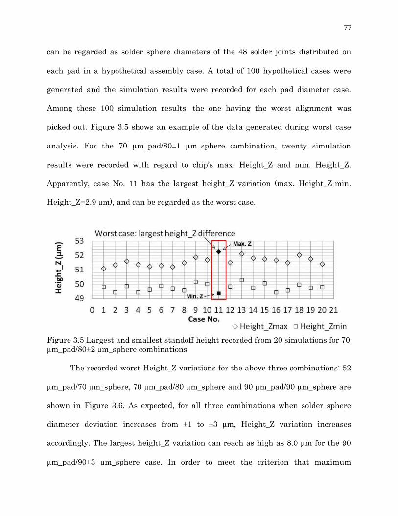
77
can be regarded as solder sphere diameters of the 48 solder joints distributed on
each pad in a hypothetical assembly case. A total of 100 hypothetical cases were
generated and the simulation results were recorded for each pad diameter case.
Among these 100 simulation results, the one having the worst alignment was
picked out. Figure 3.5 shows an example of the data generated during worst case
analysis. For the 70 µm_pad/80±1 µm_sphere combination, twenty simulation
results were recorded with regard to chip‟s max. Height_Z and min. Height_Z.
Apparently, case No. 11 has the largest height_Z variation (max. Height_Z-min.
Height_Z=2.9 µm), and can be regarded as the worst case.
Figure 3.5 Largest and smallest standoff height recorded from 20 simulations for 70
µm_pad/80±2 µm_sphere combinations
The recorded worst Height_Z variations for the above three combinations: 52
µm_pad/70 µm_sphere, 70 µm_pad/80 µm_sphere and 90 µm_pad/90 µm_sphere are
shown in Figure 3.6. As expected, for all three combinations when solder sphere
diameter deviation increases from ±1 to ±3 µm, Height_Z variation increases
accordingly. The largest height_Z variation can reach as high as 8.0 µm for the 90
µm_pad/90±3 µm_sphere case. In order to meet the criterion that maximum

78
height_Z variation should be less than 2 µm, solder sphere diameter‟s standard
deviation must be kept within ±0.8 µm. Since manufacturing variation for volume
controlled solder spheres is ±2 µm [65], none of the above three combinations is able
to meet such stringent requirement.
Figure 3.6 Height_Z variation versus solder sphere diameter deviation recorded
from worst case analysis of three different design combinations: 52 µm_pad/70
µm_sphere, 70 µm_pad/80 µm_sphere and 90 µm_pad/90 µm_sphere
On the other hand, worst case analysis indicate that chip‟s planar
misalignments, i.e., misalignment in X and Y directions misalign_x and misalign_y,
and rotation angle about Z axis theta_z are very small compared to height_Z
variation. The worst planar misalignments recorded from 70 µm_pad/80 µm_sphere
combination are shown in Figure 3.7. It is seen that although misalign_x,
misalign_y, and theta_z increases with the increasing of solder sphere diameter
deviation, they are all in the range of less than 10e-4. Therefore, it is much easier to

79
meet ±2 µm planar misalignment requirement even with large width-to-length
aspect ratio.
Figure 3.7 Planar misalignment versus solder sphere diameter deviation recorded
from worst case analysis of 70 µm_pad/80 µm_sphere design combination
3.4.2 Solder Joint Bridging Control
With the advance of high performance VCSELs packaging towards higher
interconnect densities and smaller packaging dimensions, solder bridging is
becoming more and more common. Therefore, the model should be able to predict
maximum radius (equator radius) of individual solder joints to avoid solder bridging
to the best. In the 3D model, the equator radius of the truncated solder joint was
calculated from equation (3.1) [10]:
)1.3(2
2
2
30
r
h
Vr

80
Again, V is the volume of solder joint, h is standoff height of the truncated
joint, r0 is solder‟s equator radius, and r is bonding pad radius. Bridging would
happen if equator radius of neighboring solder joints adds up to the pitch of solder
pad, e.g. 126 µm in our case. As a rough estimation, solder joint‟s maximum equator
radius should be limited to be less than 63 µm. Through worst case analysis, Figure
3.8 recorded maximum solder joint equator radius versus ±1, ±2, and ±3 µm solder
diameter deviation for 52 µm_pad/70 µm_sphere, 70 µm_pad/80 µm_sphere and 90
µm_pad/90 µm_sphere combinations. From Figure 3.8, the maximum joint equator
radius can reach as high as 61.2 µm for the 90 µm_pad/90 µm_sphere design with
±3 µm diameter deviation, indicating that this combination should be avoided since
large potential of solder bridging may happen. Whearas both 52 µm_pad/70
µm_sphere and 70 µm_pad/80 µm_sphere combinations have less than 55 µm joint
equator radius at ±3 µm diameter deviation, giving no evidence of bridging even for
the worst situations.

81
Figure 3.8 Maximum solder equator radius versus solder sphere diameter deviation
recorded from worst case analysis of three different design combinations: 52
µm_pad/70 µm_sphere, 70 µm_pad/80 µm_sphere and 90 µm_pad/90 µm_sphere
3.4.3 New Design for Better Alignment Accuracy Control
From the above analyses, it is clear that for the current solder manufacturing
tolerance (±2 µm) and the above two-row design, it‟s difficult to reach required
alignment accuracy through solder self-aligning assembly. Therefore, we proposed a
new design which allows larger manufacturing tolerance on solder volume
deviation/variation. Figure 3.9 shows the concept of the design. The new design
consists of two rows of VCSEL I/O interconnect pads and 8 extra rows of self-
alignment pads, resulting in a total of 240 bonding pads, as shown in Figure 3.9a.
The new design adopts 70 µm_pad/80 µm_sphere design combination for the best
control of solder bridging and manufacturability. In Figure 3.9a, the red color circles

82
represent solder pads and the black color circles represent model predicted joint
equators, which can be used to visually check the possibility of solder bridging. The
overall dimension of the chip is 3.2 mm×1.5 mm, and the top-view image of the chip
on substrate through 6DOF model output is shown in Figure 3.9b.

83
Figure 3.9 Proposed new design to achieve better self-alignment accuracy with large
volume variation: (a) solder pad distribution of the new design (b) top-view image of
the chip on substrate
Worst case analysis on the 240-pad design revealed that the new design can
reduce standoff height variation substantially compared to the previous 48-pad
design. Figure 3.10 compared Height_Z variation versus solder sphere diameter
deviation for the two designs. It is seen that if solder diameter variation is around
±2 µm, the standoff height variation of the 240-pad design is about 2 µm. For ±3 µm
solder sphere diameter deviation, the standoff height variation of the 240-pad
design still can be controlled to be within 4 µm (3.2 µm).
Figure 3.10 Height_Z variation versus solder sphere diameter deviation recorded
from worst case analysis of 48-pad design and 240-pad design
The reason that the 240-pad design is able to reduce standoff height variation
is that this design enlarges the chip‟s dimension along Y direction. As a result, there
is less possibility to have large height_Z variation along Y direction; also chip‟s
rotation about X-axis is reduced substantially. Figure 3.11 shows that the largest

84
rotation angle about X-axis of 48-pad design is about 10 times larger than the 240-
pad design.
Figure 3.11 Chip rotation along X axis versus solder sphere diameter deviation
recorded from worst case analysis for 48-pad design and 240-pad design
Figure 3.12 compared the maximum solder joint equator radius of the 48-pad
and the 240-pad designs. It is seen that maximum solder joint equator radius in the
240-pad design is comparable to that of the 48-pad design, and shows no evidence of
bridging even for ±3 µm solder diameter deviation.

85
Figure 3.12 Solder maximum equation radius versus solder sphere diameter
deviation recorded from worst case analysis of 48-pad design and 240-pad design
3.4.4 Discussion
Among the various parameters input to the model, solder surface tension
coefficient is an important parameter that determines shear and normal restoring
forces of a solder joint. Therefore, the accuracy of the model output is greatly
influenced by the input value of surface tension coefficient. However, solder surface
tension varies from material to material and subject to change with increasing of
reflow temperature. For instance, the surface tension coefficient of SAC related
solder materials being reported ranges from 390 to 510 dyne/cm [66]. Therefore, it is
critical to understand the influence of surface tension coefficient on model output.
Figure 3.13 shows chip‟s average standoff height at different surface tension
coefficient predicted by the model. It is seen that for the 240-pad VCSELs design,

86
changing surface tension coefficient from 300 to 600 dyne/cm only slightly varies
chip‟s standoff height by 0.1 µm, indicating that for the current VCSELs design, the
6DOF model is accurate enough and the results will not be affected significantly by
large surface tension coefficient variation.
Figure 3.13 Model predicted chip‟s average standoff height at different surface
tension coefficient
The reason that surface tension coefficient has very little influence on chip‟s
standoff height is that the current VCSELs device has a very small mass and the
joints are not subjected to large compression and will take on near geometric
equilibrium shape. Since most optoelectronic devices are small in size and low in
mass, therefore, calibration of solder surface tension coefficient is not needed for

87
their modeling. However, if chip‟s mass is large enough that solder joints
significantly collapse, surface tension coefficient will greatly affect model outputs.
Figure 3.14 shows the model predicted chip‟s average standoff height with the
increasing of chip‟s mass at surface tension coefficient of 300, 460 and 600 dyne/cm.
It is seen that when the chip‟s mass is less than 0.05 grams, chip‟s standoff height
difference between 300 and 600 dyne/cm surface tension is less than 1 µm. Such
standoff height difference becomes significant when the chip‟s mass increases to
over 0.1 grams. And the unit with 300 dyne/cm surface tension coefficient collapses
much faster than the one with 600 dyne/cm surface tension coefficient. Therefore,
for the model to be valid to heavy optoelectronic devices that is greater than 0.1
grams (for 240-pad design), it would be crucial to characterize solder‟s surface
tension coefficient through experiments.

88
Figure 3.14 Model predicted chip‟s standoff height versus chip‟s mass for
different surface tension coefficient
3.5 Chapter Summary
In this chapter, the 6DOF solder self-alignment model was used to explore
design widows of 1x12-arrayed VCSELs for flip-chip self-aligning assembly, and
was proved to be a powerful tool in the design of precision flip-chip optoelectronic
modules by providing quantitative tolerances guidelines. Worst case analysis was
performed using the model to compare the three pad/sphere combinations, such as
52 µm_pad/70 µm_sphere, 70 µm_pad/80 µm_sphere and 90 µm_pad/90 µm_sphere,
in an attempt to achieve 50 µm target chip standoff height, and to determine the

89
manufacturing tolerances of solder volume deviation/variation for each combination.
It was found out that 90 µm_pad/90 µm_sphere combination shows high potential of
bridging and should be avoided. For an initial two-row 48-pad design, solder
spheres used for chip bumping must have a diameter manufacturing tolerance
within ± 0.8 µm to achieve less than 2 µm height_Z variation, and this tolerance can
be improved to ± 2 µm through a proposed ten-row 240-pad design. For the 240-pad
design, when the mass of the optoelectronic device is less than 0.5 grams, the
variation of solder surface tension coefficient has very little effect on simulation
results. However, for the model to be valid in heavy optoelectronic devices, it would
be necessary to characterize surface tension coefficient of solder materials through
experiments.

90
CHAPTER 4 EFFECTS OF INSUFFICIENT WETTING AND SOLDER VOIDS ON
SOLDER SELF-ALIGNMENT
4.1 Introduction
In this chapter, we will attempt to identify the primary undesirable static
factors affecting solder self-alignment in the practice of industry manufacturing.
Their effects are characterized by force balance between molten solder‟s restoring
and normal reaction forces and gravity. These static effects can be used to explain
most of experimental observations. In the next chapter, we will expand such a
model to consider a dynamic situation including the self-aligning motion and
viscous damping.
Through elaborately designed experiments, we will try to figure out these
factors. Meanwhile, we will use the self-alignment model developed in chapter 2 to
build quantitative relationships between these factors and the resulted
misalignments. We will also try to answer questions such as, among the various
parameters affecting self-alignment accuracy, which plays the most important role?
How and in what range will it affect alignment accuracy? Can we reduce their
effects through optimized design? Can we avoid them through appropriate process
control? Through the studies of this chapter, we will not only be able to get a clear
picture on how many factors in manufacturing practices will affect self-alignment
accuracy, but also provide solutions to minimize the influences of these undesirable
factors.

91
4.2 Background
As has been discussed in the background review, investigations on static
factors affecting alignment accuracy has been mainly focused on maximizing
restoring forces at ideal manufacturing conditions, such as, pad size and shape
design optimization [40], pad pitch optimization [7], solder volume optimization [19].
On the other hand, extensive efforts have been put to reach optimal manufacturing
conditions for solder self-alignment, such as, reflow temperature and atmosphere
control [35], solder material and pad metallization selection [67], bumping method
selection and control [68]. For instance, Kallmayer et al. [69] investigated the
optimal reflow atmosphere for eutectic gold/tin solders to achieve good wetting and
thus good alignment accuracy. However, when manufacturing conditions are not
ideal, and manufacturing defects are inevitable, how will they quantitatively affect
alignment accuracy? Can we reduce their impacts through a better design? Related
research is absent.
One of the common problems encountered in manufacturing environments is
incomplete wetting, in which the solder partially wets a pad, resulting in a defective
solder joint. This wetting problem may be aggravated when the solders are
connected directly on bare copper pads for economic reasons, or when gas flux
soldering technology is adopted, where the reflow environments and gas activations
are more difficult to control [42,69]. Another soldering defect normally encountered
is soldering voids, whose formation mechanism is very complicate and still not very

92
well understood. Many researchers [54], [55], [67], [69] have addressed these
phenomena during the investigations on flip-chip assembly, but their focus has
been mainly on solderability [54] and reliability examination [55,67], and none of
the researches have been able to quantitatively relate these undesirable factors to
alignment accuracy, not to mention modeling their effects in order to design for
assembly. Therefore, in this chapter, we will quantitatively investigate influences of
manufacturing defects on alignment accuracy, and utilize the 6DOF model to guide
the design to minimize the influences of these factors. In addition, we will study the
influences of reflow process on the formation of soldering defects, in an attempt to
eliminate these defects through process control in manufacturing environments.
4.3 Insufficient Wetting and Modeling
4.3.1 Test Vehicle
Glass-on-silicon flip-chip test vehicles were designed and fabricated. The test
vehicle‟s design layout and assembly have been previously shown in Figure 2.5 and
2.6 in chapter 2. The UBM pads and alignment marks were fabricated through
copper electroplating, lithography, and wet etching with a target of 4 µm thickness.
A thin titanium layer of 30 nm was applied prior to copper deposition to enhance
adhesion between copper and the substrate. AZ P4620 positive photoresist
(Microchem Inc.) and Suss MJB4 mask aligner were used for pattern transfer. With
careful control of lithography protocol, high pattern transfer accuracy with
tolerance less than 200 nm was achieved. The solder used for the experiment was

93
eutectic SnPb (37/63 Pb/Sn) and its volume was controlled at 4.38±0.3 ×106 µm3 by
using volume-defined micro solder balls from Indium Corp. Eutectic SnPb alloy was
adopted because it has been the most commonly used soldering material in the
electronic industry and has superior wetting capabilities on copper surfaces [70],
good manufacturability, and process compatibility [71]. The solder balls were first
placed on the solder pads on the silicon substrate manually with tweezers and
reflowed to form spherical cap bumps. Then a dummy glass chip of 0.005±0.0006
grams in weight was placed to cover the bumped substrate with an initial pick-and-
place accuracy of around 30 µm. Finally, another reflow was performed to form
solder connections and achieve self-alignment. This assembly process is compatible
with most optoelectronic devices such as light-emitting diodes (LEDs) and vertical-
cavity surface-emitting lasers (VCSELs), which are susceptible to contamination
and thus usually prohibited from solder bumping. A formic acid-based fluxless
soldering reflow process [42], which is preferable for optoelectronics packaging to
avoid contamination from chemical flux, was employed for the soldering. The
introduction to the reflow process and schematic diagram of the reflow setup were
shown previously in Figure 2.9 in chapter 2. A total of 10 test vehicles were
assembled using this reflow technology during the study.
The overall misalignments of the chip relative to the substrate, defined as
misalignment in X direction, misalign_x, misalignment in Y direction, misalign_y,
and rotation angle at the center point of the chip, θ, can then be calculated through
the following equation sets:

94
(4.1)
where (x1, y1) and (x2, y2) are Cartesian coordinates of two individual pads
located on the substrate, and (x1′, y1′ ), (x2′, y2′ ) are the coordinates of the pads on
the chip opposite to the above two, which can be read directly from the optical
microscopic observation of the alignment mark sets. Input the known parameters
(x1, y1), (x2, y2), and (x1′, y1′), (x2′, y2′) into equation (4.1) yields misalign_x,
misalign_y, and θ. A schematic drawing of a misaligned chip-to-substrate system
indicating all the aforementioned parameters is shown in Figure 4.1.
)1(
_cos2sin22
_cos1sin11
_sin2cos22
_sin1cos11
ymisalignyxy
ymisalignyxy
xmisalignyxx
xmisalignyxx

95
Figure 4.1 Diagram of a misaligned chip-to-substrate system illustrates all the
parameters appeared in equation (4.1)
4.3.2 Experimental Results
The assembled test vehicles showed large variation in alignment accuracy.
Microscopic photographs of two representative samples are shown in Figure 4.2 and
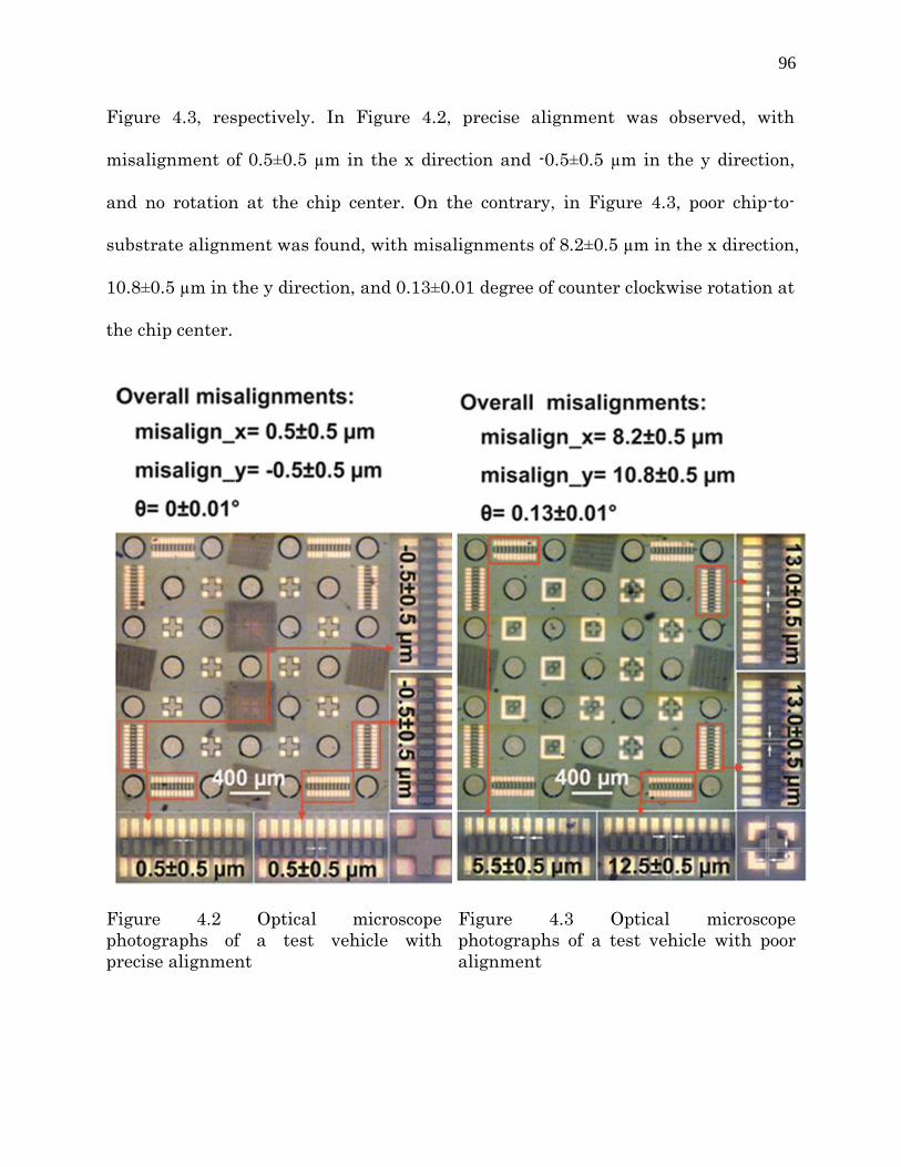
96
Figure 4.3, respectively. In Figure 4.2, precise alignment was observed, with
misalignment of 0.5±0.5 µm in the x direction and -0.5±0.5 µm in the y direction,
and no rotation at the chip center. On the contrary, in Figure 4.3, poor chip-to-
substrate alignment was found, with misalignments of 8.2±0.5 µm in the x direction,
10.8±0.5 µm in the y direction, and 0.13±0.01 degree of counter clockwise rotation at
the chip center.
Figure 4.2 Optical microscope
photographs of a test vehicle with
precise alignment
Figure 4.3 Optical microscope
photographs of a test vehicle with poor
alignment

97
To identify the key factor that causes the alignment variation, the above
samples were cleaved with a sharp razor blade along the gap between chip and
substrate and separated into two parts. Figure 4.4 and Figure 4.5 reveal the
surfaces of the glass chip and the silicon substrate after the above two samples were
disassembled. For the sample with poor alignment, as shown in Figure 4.4, residual
copper was clearly observed on many solder pads (Figure 4.4a), and their solder
counterparts showed irregular shapes on the top (Figure 4.4b), indicating the
existence of incomplete wetting. In contrast, for the sample with precise alignment,
as shown in Figure 4.5, all the solders fully covered the solder pads and no obvious
residual copper was found.

98
Figure 4.4 Optical microscope
photographs of a disassembled test
vehicle with incomplete wetting where:
(a) residual copper was observed on
several UBM pads located on the glass
chip and (b) irregular shapes were found
for solder bumps on the silicon
substrate.
Figure 4.5 Optical microscope
photographs of a disassembled test
vehicle with complete wetting where: (a)
no residual copper was observed on
UBM pads located on the glass chip
and, (b) round shapes were found for
solder bumps on the silicon substrate.
Scanning electron micrographs (SEM, JSM-6480LV, Joel Limited) in Figure
4.6 further revealed that completely wetting of solder bumps guarantees good
alignment between the chip and the substrate through forming perfectly

99
symmetrical shapes. The magnified image in Figure 4.6b shows a perfect truncated
bump. When incomplete wetting occurs, however, solder joints were distorted,
causing degradation of the self-alignment. SEM images in Figure 4.6c and d reveal
an array of distorted solder bumps and a representative defective bump,
respectively.

100
Figure 4.6 SEM images of solder bumps in assemblies with different wetting
conditions show: (a) an array of completely wetting solder bumps with perfect
symmetry (b) a representative perfect truncated bump (c) an array of distorted
solder bumps due to incomplete wetting (d) a representative defective bump
Further investigation indicates that among the 10 assembled test vehicles, 3
samples had incomplete wetting defects and showed an average overall
misalignment larger than ±10 µm both in X and Y directions. Meanwhile, solder
joints in the other 7 samples (reflowed with auxiliary resin flux) fully wetted the
pads and alignment accuracy less than ±1 µm was achieved. In addition, given that
there are solder volume variation of around 5% and solder pad diameter deviation
of around 0.2 µm in those precisely aligned samples, it is reasonable to conclude
that the manufacturing tolerance related factors contribute minimally to post-
assembly misalignments.
4.3.3 Modeling on Insufficient Wetting
The 6DOF model developed in chapter 2 cannot be directly applied to the
joints with irregular shape, such as those in the incomplete wetting cases. It is also
impractical to build a Surface Evolver model for individual defective solder joints
because of the large number of solder connections being employed in one assembly.
Therefore, in the following section, we will estimate the restoring force generated by
incomplete wetting joints through a simplified method to modify the 6DOF quasi-
static force optimization model, so that it can simulate the insufficient wetting
phenomenon.

101
The chip on substrate system was originally designed to have well-aligned
top and bottom bonding pads. However, incomplete wetting modifies the effective
configuration of the pad, and introduces a permanent lateral alignment offset
among the bonding pad pair. Such alignment offset is the origin of large chip-to-
substrate misalignments and should be regarded as initial conditions for model
inputs. An example of how to determine the incomplete wetting introduced
alignment offset of each bonding pad pair is illustrated in Figure 4.7. Residual
copper with bright yellow contrast was first carefully identified on each pad. Then
circles were drawn on the pads to ensure that the copper residues are excluded from
the circles. These circles represent the adjusted positions of the pads to account for
the effect of the incomplete wetting. The diameter of the circles is the same as the
diameter of the solder pads. In Figure 4.7, the adjusted positions of the pads are
outlined by white circles, and the inset on the top right corner shows the shift of the
pad from the initially designed position to the adjusted position. The shift vector
index (-50, 30) indicates that a shift of -50 µm along X axis and 30 µm along Y axis
was made to the pad, which also implies the alignment offset between the top and
the bottom pads is (-50, 30). In such a manner, all the boding pads offsets in the
three incomplete wetting samples were measured.

102
Figure 4.7 Diagram shows methodology to identify incomplete wetting introduced
alignment offsets by excluding residual copper from the original pads
It is noted that the chip shown in Figure 4.7 needs to be flipped over to finish
the assembly, and therefore the location of individual pads needs to be adjusted to
accommodate the flip over of the chip. The new arrangement of these pads after
chip‟s upside-down flip over is shown in Figure 4.8. In the Figure 4.8, the dashed
circles represent the initial designed position of the pads and the solid circles
represent the adjusted position of these pads as a result of incomplete wetting, with

103
indexes denoting the vector of the shift. The above parameters for model inputs are
summarized in Table 4.1, which lists the location (represented by Cartesian
coordinate index) of each bonding pad along with its alignment offset introduced by
incomplete wetting.

104
Figure 4.8 Diagram shows alignment offsets of the soldering pads after chip‟s
upside-down flip over
Table 4.1 Model inputs: solder pad locations and their respective alignment offsets
introduced by incomplete wetting (in µm)
Pad No. Location Alignment Offset Pad No. Location Alignment Offset
1-1 (-1200, 1200) (-55, -35) 4-3 (800, 0) (-30, -20)
1-2 (-400, 1200) (0, 0) 5-1 (-1200, -400) (0, 0)
1-3 (400, 1200) (0, 0) 5-2 (-400, -400) (-30, -60)
1-4 (1200, 1200) (0, 0) 5-3 (400, -400) (-60, -20)
2-1 (-800, 800) (-15, -35) 5-4 (1200, -400) (0, 0)
2-2 (0, 800) (-55, -20) 6-1 (-800, -800) (-20, -12)
2-3 (800, 800) (0, 0) 6-2 (0, -800) (-20, 0)
3-1 (-1200, 400) (-40, -25) 6-3 (800, -800) (0, 0)
3-2 (-400, 400) (-35, -25) 7-1 (-1200, -1200) (0, 0)
3-3 (400, 400) (-20, -30) 7-2 (-400, -1200) (-20, 0)
3-4 (1200, 400) (0, 0) 7-3 (400, -1200) (0, 0)
4-1 (-800, 0) (-20, -60) 7-4 (1200, -1200) (0, 0)
4-2 (0, 0) (-50, -30)
The origin of the coordinate system (0, 0) is at the center of the chip, and the
pad‟s serial number “1-1” indicates that the pad is located in the first row and first
column of the array. Other design and manufacturing parameters input to the
model are listed in Table 4.2.
Table 4.2 Model inputs: design and manufacturing parameters of the test
vehicle
Classification Specified items Value
Initial design
parameters
Pad diameter 200 µm
Surface tension coefficient 325 gram/s2
Chip mass 0.005 gram
Chip length 3000 µm
Chip width 3000 µm

105
Chip thickness 175.0 µm
Solder volume 4.38±0.3 × 106 µm3
Initial external
forces
External loadings in x, y, and z directions
and external moments around x, y, and z
axis
[ 0 0 0 0 0 0 ]'
Direction of gravity vector [0, 0, -1] (its value is [0, 0, -1] if
the assembly does not tilt at all)
Initial chip
position
Chip initial lateral misalignment in micron
[x, y] [25, 10]
Chip initial standoff height 40 µm
These parameters include: 1) initial design parameters, such as pad diameter
(200 µm), chip mass (0.005 grams), chip size (3 mm × 3 mm × 0.175 mm), solder
volume (4.38±0.3 × 106 µm3, randomly distributed on each pad), as well as solder
surface tension coefficient (325 gram/s2 [17]); 2) initial external forces, including
reflow platform tilting represented by the gravity vector‟s direction and other
external forces imposed on the chip, which is zero in the present study, and 3)
initial chip‟s position before solder reflow which reflects the pick and place accuracy
of the chip, and was found to be about 25 µm in the X direction and 10 µm in the Y
direction. It is noted that chip‟s pick and place position determines only the initial
value of the state vector U, by doing so it will affect the starting point of the
iteration path for model convergence. However, it has no effect on the equilibrium
condition of the assembly, and U will be converged to zero no matter what its initial
value is. Therefore, the output of the model, i.e., the predicted alignment accuracy
will not be affected by chip‟s initial pick and place position. By contrast, incomplete
wetting altered the equilibrium condition of the chip by introducing permanent
misalignment between chip and substrate, and will affect the final alignment
accuracy substantially.

106
The results from the model for the above inputs are shown in Figure 4.9.
With 12-60 m as the characteristic widths of incomplete wetting areas in 14 out of
the total 25 solder joints, the model predicts chip‟s overall lateral misalignments
x=19.0 m, y=15.0 m, and rotation angle θz= -0.19°. Figure 4.9a displays the
visualized output of the model, where the inner white square represents chip and
the outer green square represents substrate. The calculated misalignments at each
corner of the chip are labeled in Figure 4.9a. This simulation result is very close to
that of the real assembly measured with microscope, implying the validity of the
methodology used in the model. As shown in Figure 4.9b, the misalignments of four
individual points at each corner of the flip-chip system were characterized with
microscope and the chip‟s overall misalignments were calculated to be
misalign_x=20.5±0.5 m, misalign_y=17.5±0.5 m, and θ=-0.16±0.01° using the
above mentioned Equation (4.1).

107
Figure 4.9 Comparison between (a) modeling and (b) experimental results for an
incomplete wetting case.
Listed in Table 4.3 are individual alignment offsets of the bonding pad pairs
in sample #1 and #2. It is noted that only those pads poorly wetted by the solder are
listed in the table, and the pads that are not listed showed complete wetting and
had default alignment offset of (0, 0).
Table 4.3 Model inputs for sample #1 and sample #2: solder pad locations and their
respective alignment offsets introduced by incomplete wetting (in µm)
sample #1 sample #2
Pad No. Location Alignment Offset Pad No. Location Alignment Offset
1-1 (-1200, 1200) (30, -30) 3-2 (-400, 400) (40, 20)
1-3 (400, 1200) (-15, -15) 3-3 (400, 400) (-10, -25)
3-1 (-1200, 400) (65, -20) 4-1 (-800, 0) (20, -6)
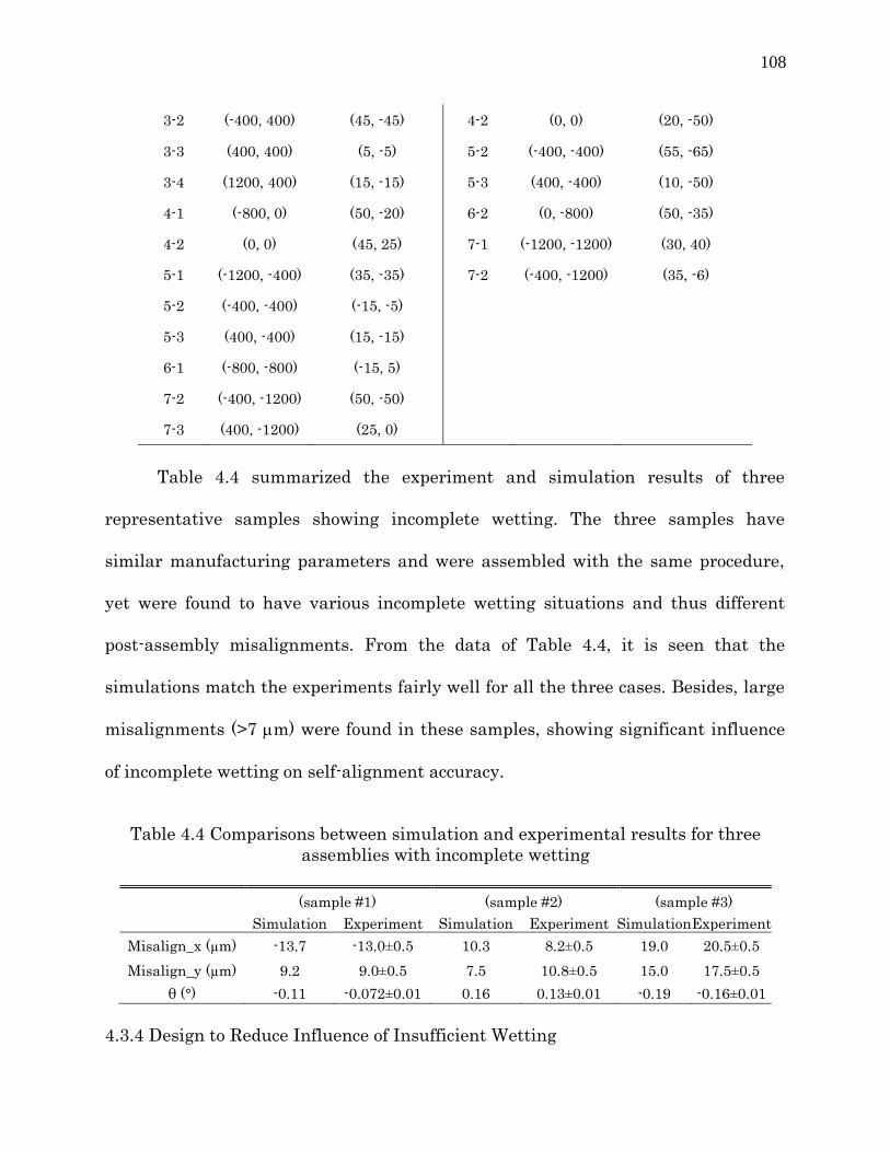
108
3-2 (-400, 400) (45, -45) 4-2 (0, 0) (20, -50)
3-3 (400, 400) (5, -5) 5-2 (-400, -400) (55, -65)
3-4 (1200, 400) (15, -15) 5-3 (400, -400) (10, -50)
4-1 (-800, 0) (50, -20) 6-2 (0, -800) (50, -35)
4-2 (0, 0) (45, 25) 7-1 (-1200, -1200) (30, 40)
5-1 (-1200, -400) (35, -35) 7-2 (-400, -1200) (35, -6)
5-2 (-400, -400) (-15, -5)
5-3 (400, -400) (15, -15)
6-1 (-800, -800) (-15, 5)
7-2 (-400, -1200) (50, -50)
7-3 (400, -1200) (25, 0)
Table 4.4 summarized the experiment and simulation results of three
representative samples showing incomplete wetting. The three samples have
similar manufacturing parameters and were assembled with the same procedure,
yet were found to have various incomplete wetting situations and thus different
post-assembly misalignments. From the data of Table 4.4, it is seen that the
simulations match the experiments fairly well for all the three cases. Besides, large
misalignments (>7 m) were found in these samples, showing significant influence
of incomplete wetting on self-alignment accuracy.
Table 4.4 Comparisons between simulation and experimental results for three
assemblies with incomplete wetting
(sample #1) (sample #2) (sample #3)
Simulation Experiment Simulation Experiment Simulation Experiment
Misalign_x (µm) -13.7 -13.0±0.5 10.3 8.2±0.5 19.0 20.5±0.5
Misalign_y (µm) 9.2 9.0±0.5 7.5 10.8±0.5 15.0 17.5±0.5
θ (°) -0.11 -0.072±0.01 0.16 0.13±0.01 -0.19 -0.16±0.01
4.3.4 Design to Reduce Influence of Insufficient Wetting

109
Equipped with the above modified self-alignment model, we are now ready to
design to reduce adverse effect of insufficient wetting on self-alignment accuracy.
The model further reveals that if the incomplete wetting introduced alignment
offset vectors had been predetermined; it would not be possible to improve the chip‟s
alignment accuracy by changing solder volume, pad diameter, surface tension
coefficient, or chip mass. This is because the lateral restoring force is linearly
proportional to the alignment offset of the bonding pad pair, and the above
mentioned parameters only determine the coefficient of the proportionality. The
changing of the above parameters only proportionally varies the restoring force of
each joint, however, the chip‟s equilibrium condition as a whole (in which the sum of
restoring forces is zero) does not change at all. On the other hand, the position
layout of the bonding pads does have an influence on alignment accuracy. For
instance, by placing the bonding pads closer to each other, i.e. reducing the pad
pitch from 800 to 400 µm, as shown in Figure 4.10a, while keeping the other
parameters (alignment offsets and pad diameters) the same, the chip‟s rotation
angle increased from 0.19 to 0.38 degree (Figure 4.10b). On the contrary, if the pitch
was increased from 800 to 1600 µm (Figure 4.11a), the chip‟s post-assembly rotation
angle was reduced by half (Figure 4.11b), indicating that large pitch is preferable
for reducing incomplete wetting caused misalignment. However, this type of layout
modification has no effect on reducing misalignments in X and Y direction. As listed
in Table 4.5, with the increasing of pad pitch, the rotation angle θ decreased
substantially, while lateral misalignments misalign_x and misalign_y remained the

110
same. The minute variations in misalign_x and misalign_y were due to the random
distributions of solder volume on the bonding pads in each simulation. Therefore, by
increasing bonding pad pitch, we can reduce the insufficient wetting caused
rotational misalignment.

111
Figure 4.10 (a) A hypothetical layout design of bonding pads and their individual
incomplete wetting conditions (the pad pitch was reduced to 400 µm and the other
parameters were kept the same). (b) Simulation results for the above design.
Figure 4.11 (a) A hypothetical layout design of bonding pads and their individual
incomplete wetting conditions (the pad pitch was reduced to 1600 µm and the other
parameters were kept the same). (b) Simulation results for the above design
Table 4.5 Simulated misalignments of three hypothetical assemblies with different
pad pitches
400 µm pitch 800 µm pitch 1600 µm pitch
Misalign_x (µm) 18.7 19.0 18.9
Misalign_y (µm) 14.7 15.0 14.5
θ (°) -0.38 -0.19 -0.096
4.4 Solder Voids and Modeling
4.4.1 Test Vehicle
The test vehicle used for the investigation on solder self-alignment accuracy
is shown in Figure 4.12. It is a 1x12-arrayed dummy VCSELs (3200 × 500 × 650
µm), which features 12 identical VCSEL chips. Each chip has a dimension of 220 ×

112
500 × 650 µm3 and composes 4 bonding pads for electrical/mechanical connection.
Pitch between neighboring bonding pads is 126 µm. Total mass for the VCSEL-
array is 0.0054±0.0002 gram. Volume controlled SAC (96.5%Sn-3%Ag-0.5%Cu)
solder spheres were used for interconnects. The diameter of bonding pad is 70 µm
and the diameter of solder sphere is 80 µm. The fabrication, assembly, and reflow
process of the dummy VCSELs are similar to the test vehicle previously introduced
in chapter 3. The reflow process for this test vehicle is also a formic acid-based
fluxless soldering process, and process details have been introduced in the previous
section in chapter 2. Different from the 220 ℃ reflow temperature used for eutectic
Pb/Sn solder in section two, the peak reflow temperature for this assembly is 250 ℃.
In addition, the formic acid concentration used for the assembly is increased to
around 1.5%. A total of 9 samples were assembled. Because this kind of assembly
has only two rows of solder joint, a more detailed observation on each single joint
becomes possible.
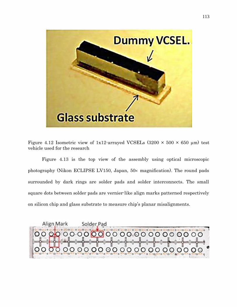
113
Figure 4.12 Isometric view of 1x12-arrayed VCSELs (3200 × 500 × 650 µm) test
vehicle used for the research
Figure 4.13 is the top view of the assembly using optical microscopic
photography (Nikon ECLIPSE LV150, Japan, 50 magnification). The round pads
surrounded by dark rings are solder pads and solder interconnects. The small
square dots between solder pads are vernier-like align marks patterned respectively
on silicon chip and glass substrate to measure chip‟s planar misalignments.

114
Figure 4.13 Top view of the 1×12 VCSEL chip array assembly using optical
microscopic photograph. The assembly include flip-chip bonded silicon chip onto
glass substrate using SAC lead-free solders.
4.4.2 Experimental Results
It was found out that big soldering voids appeared in the assembly reflowed
at a formic acid concentration of about 1.5%. From the cross-section images in
Figure 4.14, big voids were observed in four joints from a total of exposed 12 joints.
Figure 4.14 Assembled unit reflowed with 1.5% formic acid vapor contains large
visible voids
The existence of large numbers of visible voids was further confirmed by X-
ray inspection, as shown in Figure 4.15. Big voids were found in 40 joints out of the
entire 48 interconnects and the largest voids has a diameter of around 46 µm. The
number listed on top and bottom of each solder joint is diameter of the solder joint
and the voids measured from the image. However, due to low resolution of the X-ray

115
image, the measured results from these images are not as accurate as those from
optical microscopic photography.
Figure 4.15 X-ray inspection of the assembly shows big visible voids in solder
joint connections
Experiments further revealed that compared to those units without voids,
units contain large amount of voids demonstrate large average standoff height. As
shown in Figure 4.14, an average 54 µm standoff height was observed for the unit
shown in the image containing large visible voids, while the one shown in Figure
4.16 without obvious voids has an average standoff height of only 51 µm. Listed in
table 4.6 are the measured misalignments of the VCSEL samples reflowed at
different atmospheres: sample #1 to #3 were reflowed with resin flux and sample #4
to #9 were reflowed with formic acid vapor at 1.5% volume concentration. The data
clearly evident that samples with large visible voids have higher standoff height.
On the other hand, solder voids seems to have no obvious influence on planar
alignment accuracy as all the assembled units have good alignment in X-Y plane no
matter contain voids or not.

116
Figure 4.16 Assembled unit reflowed with resin flux contains no visible voids and
has small average chip standoff height
Table 4.6 Measured misalignments of the VCSEL samples reflowed at different
atmospheres
Sample
No.
Misalign_x
(µm)
Misalign_y
(µm)
Max. height_Z
(µm)
Min. height_Z
(µm)
#1 0±0.5 0.5±0.5 53.8±0.2 51.9±0.2 Small Visible
Voids
(UBM thickness
included)
#2 0±0.5 0±0.5 51.5±0.2 50.9±0.2
#3 0±0.5 0±0.5 52.1±0.2 50.5±0.2
#4 0±0.5 0 ±0.5 54.9±0.2 53.4±0.2
Large Voids
Observed
(UBM thickness
included
#5 0±0.5 0.5±0.5 58.2±0.2 56.4±0.2
#6 0±0.5 -0.5±0.5 56.8±0.2 55.2±0.2
#7 0±0.5 0±0.5 61.5±1.5 58.6±1.5
#8 0±0.5 0.5±0.5 56.4±1.5 54.3±1.5
#9 0±0.5 0±0.5 57.2±1.5 54.8±1.5
4.4.3 Modeling on Solder Voids

117
The challenge with modeling voids effect on alignment accuracy lies on the
accurate determination of the voids concentration. Our early attempts to evaluate
the volume percentage of the voids using X-ray image failed because the resolution
of X-ray is very low and it intends to underestimate the volume of the voids,
especially those voids with smaller size. In this section, we will be using solder
joint‟s geometric profile to calculate the total volume of the joint containing voids,
and voids volume can be derived through subtracting solder joint‟s initial volume
from the total volume. The voids volume concentration estimation process is
described as follows:
The volume of a truncated solder joint can be calculated from the following
equation:
2
2
where V is the total volume of the joint, h is standoff height of the joint, r0 is
joint‟s equator radius, and r is bonding pad radius. It is noted that this equation is
also valid when the joint contains voids. Therefore, from measuring solder joint‟s
standoff height, equator radius, as well as bonding pad radius, its total volume Vt
including voids can be determined accordingly. As the initial volume of solder
materials Vi is a known value from the solder sphere specification sheet, which is
provided by solder sphere‟s vendor, thus the voids volume Vv contains by this joint
can be determined by:

118
And voids volume concentration Cv can be calculated from:
𝐶 ( )
During the experiments, cross-sectional examination of the assembly and
confocal microscopy were performed to determine standoff height of individual
solder joints. The maximum measurement error is about 1 µm. Solder‟s equator
radius was measured with optical microscope from the dark ring shown in Figure
4.13, and the maximum error associated to this measurement method is less than
0.5 µm.
The validation of the above methodology was made through the following
experiments. Solder spheres with known diameter Ø80 µm were used as flip-chip
interconnects in the VCSELs assembly. After bonding was finished, these joints
were cross-sectioned and their optical microscopic photographs are shown in Figure
4.17. For the first joint, its height was measured to be 53.2 µm (include
intermetallic alloy thickness) and its equator diameter is 85.2 µm, which yields a
volume that equals sphere with diameter of Ø80.2 µm from equation (4.2).
Therefore the voids volume concentration in this joint is calculated to be 0.75%,
which agrees with experiments since only tiny voids were observed from the cross-
section image. The second joint contains one big voids with diameter of 31.5 µm and
two small voids with diameters of 9.1 µm and 5.0 µm respectively, and this gives

119
the voids volume concentration of 5.9%. On the other hand, its standoff height and
equator diameter were measured to be 52.9 and 89.5 µm, and equation (4.2)
predicts that it has a voids concentration of 7.5%. The large deviation between two
measurement methods might come from the dissolving of the copper pad into solder
material forming intermetallic compounds. The volume increment from dissolved
copper is also counted as voids from equation (4.2).
Figure 4.17 Cross-sectional images of solder joint for the purpose of measuring
standoff height and equator radius
Table 4.7 compared the voids volume concentration observed directly from
cross-section and calculated from the method proposed in this research for a total of
three joints shown in Figure 4.17. It can be seen that the model predicted voids
volume concentration agrees experiments observations very well in case one and
case three. In case two, due to severe dissolving of copper pads into solder joint, the
calculated voids volume concentration is larger than that actually observed.
Table 4.7 Comparison of joint volume observed from cross-section and calculated
from the model
Experiment Observed Voids Volume Concentration Model Predicted Voids Volume
Concentration

120
Item
Joint
original
dia.
(µm)
Voids 1
dia.
(µm)
Voids 2
dia.
(µm)
Voids
3 dia.
(µm)
Voids volume
concentration
Joint
standoff
height
(µm)
Joint
equator
dia.
(µm)
Voids volume
concentration
Joint
#1 80 0 0 0 0% 53.2 85.2 0.75%
Joint
#2 80 31.5 9.1 5.0 5.9% 52.9 89.5 7.5%
Joint
#3 80 30.0 0 0 5.0% 56.9 84.3 5.8%
Using this method, a total of 3 VCSELs units were analyzed. With the
measured standoff height and equator radius of each solder joint, the volume of
individual solder joint given by equivalent sphere diameter was determined and
recorded in Figure 4.18. It is seen that the solder joints in all 3 units have
equivalent diameter much larger than their original diameter Ø80 µm, indicating
large percentage of voids exist in the units. From the data in Figure 4.18, the
average joint volume distribution for unit #1 equals to the spheres having
diameters of 86.3±1.4 µm, yields an average voids volume concentration of 20.3%.
This value becomes 84.0±1.0 µm and 83.8±1.1 µm for units #2 and #3, and as a
result the voids volume concentrations for units #2 and #3 are 13.6% and 13.0%,
respectively. Evidently unit #1 contains more voids than units #2 and #3. The joint
volume distributions in all three units shown in Figure 4.18 were then input to the
6DOF self-alignment model, and the predicted chip‟s standoff heights are shown in
Figure 4.19.

121
Figure 4.18 Solder volume distribution in the characterized 3 units that include
voids
As expected, the average chip‟s standoff height of the three samples increases
with the increasing of voids volume concentration. Unit #1 has the largest standoff
height among the three units. The model predicted height for unit #1 is 57.9-59.2
µm, which is close to experimental results 58.6-61.5 µm. For units #2 and #3, the
model predicted height is 54.9-56.7 µm and 54.8-56.2 µm, which also agree with
experimental results 54.9-56.4 µm and 54.8-57.2 µm. The solid line in Figure 4.19 is
model predicted average chip standoff height versus average voids volume
concentration in the assembly, assuming all the joints have the same volume and
voids concentration. The average standoff height lies reasonably between the
maximum and minimum standoff height of the three assemblies. It is also seen
from the average standoff height line that to keep chip‟s standoff height within 52
µm, the voids volume concentration should be less than 3.7%.

122
Figure 4.19 Solder self-alignment model predicted chip standoff height in 3 units
and average standoff height versus average voids volume concentration
4.4.4 Design to Reduce Influence of Solder Voids
From the above analysis, it is seen that chip‟s standoff height increases with
the increasing of voids volume concentration. In order to reduce the influence of
solder voids on standoff height variation, can we design the pad so that it produces
the smallest standoff height increment when the joint contains a certain amount of
voids? We are going to explore such possibility through the following example. In
chapter 3 during the design of VCSELs for self-aligning assembly, we have
identified three pad/solder sphere diameter combinations, i.e. 52 µm_pad/70
µm_sphere, 70 µm_pad/80 µm_sphere and 90 µm_pad/90 µm_sphere. Figure 4.20
shows the model simulated chip‟s standoff height increments with the increasing of

123
solder voids volume concentration for these three design combinations. It is seen
that to keep the chip‟s average standoff height increments within 2 µm, voids
volume concentration in general must be controlled within 5%. Moreover, the 52
µm_pad/70 µm_sphere design is more preferable as it shows higher resistance to
standoff height increment with the increasing of voids volume concentration
compared to the other two designs.
Figure 4.20 Chip standoff height increments with the increasing of voids volume
concentration for the three pad/solder combinations in the design of VCSELs
4.5 Reflow Process Control to Eliminate Insufficient Wetting and Solder Voids
Effects
As can be seen from the above sections, insufficient wetting and solder voids
are two major undesirable factors that significantly affect self-alignment accuracy.

124
We can reduce their effects through appropriate pad design. Alternatively, we can
improve the process itself. In this section, we are going to explore solutions that are
able to eliminate these adverse factors from improvement of the process.
Insufficient wetting and solder voids are two common packaging defects
during SMT or flip-chip assemblies. One major reason causes these defects is solder
pad oxidation which arises from insufficient reducing reflow atmosphere. It has
been reported that formic acid concentration determines the activity of reducing
atmosphere during solder reflow. For instance, Lin.W. et.al. investigated the
influence of formic acid concentration on self-alignment dynamics using Tin/Lead
solder connections [42] in a BGA packaging. They found out that the BGA board
reflowed at high formic acid concentration atmosphere finished self-alignment much
quicker than those reflowed at low formic acid concentration atmosphere. However,
the study did not mention the insufficient wetting and solder voids problems. As a
matter of fact, there have been very rare researches about the influences of formic
acid atmosphere on insufficient wetting and solder voids formation, especially for
SAC solder materials. Therefore, in the studies of this dissertation, we performed a
series of experiments trying to figure out effect of formic acid reflow atmosphere on
the formation of soldering defects such as insufficient wetting and solder voids.
The formic acid reflow setup was introduced previously in chapter 2 (refer to
Figure 2.9). In our studies, various formic acid concentrations ranging from 0.77%

125
to 4.3% were evaluated for their activities in assisting SAC soldering. The procedure
used to determine formic acid concentration is listed as follows:
Measure formic acid solution mass before reflow m1;
Measure formic acid solution mass after reflow m2;
Total formic acid vapor mass M consumed during reflow is m1-m2;
Divide the mass M with 48.6 yields mole volume of formic acid n;
According to PVf=nRT, formic acid vapor volume Vf can be determined;
N2 volume Vn=flow rate × reflow time;
Formic acid concentration is calculated from C=Vf/Vn+Vf.
Resin flux has been recognized as the most efficient material in removing
surface oxidation thus assisting wetting between bonding materials [69]. Therefore,
the first experiment was performed to compare effectiveness of resin flux versus
reflow atmosphere with different formic acid concentration in assisting wetting
between solder and the bonding pad. Figure 4.21 is schematics of the test setups.
Ø90 µm SAC solder spheres were placed on bare copper pad. Some of them were
covered by resin flux (lead free soldering paste from William H. Harvey CO., part
No. 097205) and the others were exposed directly to the reflow atmosphere. The
reflow atmosphere was composed of nitrogen and formic acid gas mixture with
formic acid vapor concentrations can be adjusted. During the experiments, hot plate

126
was turned on to heat the copper pad up until SAC melting temperature was
reached, and solder spheres began to melt and spread out driven by wetting force
between solder and the beneath copper pad. After wetting was completed, high
resolution optical microscope was used to measure spreading diameter of the solder
spheres over the copper pad.
Figure 4.21 Schematics of test setups for wetting test of Ø90 µm SAC solder at
different reflow atmospheres
Figure 4.22 shows three photographs in course of measuring solder spreading
area reflowed at different atmospheres. The first picture shows the spread of solder
spheres covered with resin flux. The second picture shows the spread of solder
spheres reflowed at an atmosphere of 1.0% formic acid concentration, and the third
picture shows the spread of solder spheres reflowed at an atmosphere of 0.7% formic
acid concentration.

127
Figure 4.22 Photographs in course of measuring Ø90 µm SAC solder spreading area
at different reflow atmosphere
The spreading diameter of solder spheres on copper pad was recorded in
Figure 4.23. It was found out that the spheres covered with resin flux have almost
constant spreading diameter of around 270 µm regardless of formic acid vapor
concentration which acts as external reflow atmospheres. The spheres reflowed
without resin flux, however, showed a gradual increase in spreading diameter with
the increasing of formic acid concentration. Solder spheres reflowed at 0.7% formic
acid concentration have smaller spreading diameter of 200 µm than those reflowed
with resin flux. When formic acid concentration reaches 1.1%, the spreading
diameter is comparable to those reflowed with resin flux of 270 µm, indicating that
formic acid concentration of 1.1% and higher is able to provide an effective reducing
atmosphere to assist spread wetting of SAC solder on copper pad and is comparable
to conventional resin flux.

128
Figure 4.23 Solder spreading diameter versus formic acid concentration for SAC
spheres wetting copper pad
Another series experiments were performed to explore mechanisms of solder
voids formation during reflow process using formic acid vapor as soldering flux.
Commercially available direct attach LED chips (Cree DA 3330) with 3 µm-thick
eutectic 80Au/20Sn bonding pads were used for the experiments. The chip was flip-
chip bonded on a PCB with Cu(18 µm)/Ni(4 µm)/Au(200 nm) as bonding pad surface
finish. It was found out that SAC interconnect between Au/Sn and Au/Ni/Cu
bonding pads reflowed at 1.1% formic acid concentration still contains large
numbers of voids, and the voids concentration is about 21%. The voids concentration
was reduced significantly to about 10% when formic acid concentration was

129
increased to 2.6%, and totally disappeared when formic acid concentration was
increased to 4.3%, as can be seen from Figure 4.24.
Figure 4.24 Voids concentration versus formic acid concentration for SAC
interconnect between Au/Sn and Au/Ni/Cu bonding pads
According to ref. [72-79], there are two key factors that cause the formation of
voids, which are, 1) Large amount of gas bubbles generated in molten solder; 2) The
bubbles do not have enough time to escape. Herein we will briefly discuss the voids
formation mechanism when using formic acid as soldering flux. When using formic

130
acid to remove surface oxidation of solder pads, the following chemical reactions will
happen:
When T>150 °C, MeO+2HCOOH=Me(COOH)2+H2O
When T>200 °C, Me(COOH)2=Me+CO2+H2 and H2+MeO=Me+H2O
where Me(COOH)2 is a kind of metal compound that covers solder pad surface
at lower temperature and then decomposes into metal, CO2 and H2 at higher
temperature. Therefore, the possible voids formation mechanism might be in the
following: As shown in Figure 4.25, low concentration formic acid could not totally
remove MeO on some areas of solder pad due to low reducing activity, as a result,
these MeO spots were covered by thin Me(COOH). At higher temperature, with the
decomposing of Me(COOH), metal begin to expose and solder wetting happens. The
fast moving wetting front entrapped those MeO in the molten solder. Together with
the MeO being entrapped should also be some hydrogen adsorption layer coming
from decomposing of Me(COOH). The hydrogen layer continues to react with MeO
and generate CO2 and water vapor bubbles inside the SAC material. These bubbles
cannot totally escape from the solder joints and form voids. From the experiments,
although 1.1% formic acid concentration is sufficient for a quality solder wetting
spread, it is still not sufficient to remove local oxidation spots, which will eventually
become the source of trapping vapors and the formation of voids.

131
Figure 4.25 Illustrations on voids formation mechanism when using formic acid as
reflow flux
It should be noted that the above proposed mechanisms are purely based on
reasonable assumptions and need a more rigorous verification through well-
designed experiments. Since the formation of voids is a very complicated topic, a
much more detailed study of voids formation mechanism is outside the scope of this
dissertation, and therefore will not be discussed further.
4.6 Chapter Summary
In this chapter, we conclude that insufficient wetting and solder voids during
formic acid-based reflow have significant influences on self-alignment accuracy.
Complete wetting of solder on bonding pads results in good alignment, while
incomplete wetting results in bad alignment caused by solder joint deformation. In
order to reduce misalignment caused by incomplete wetting, a large pitch between
the bonding pads is preferable. Solder void is another undesired factor and it
increases standoff height variation of the assembled unit. However, it imposes
almost no impact on lateral alignment. Manufacturing tolerance related factors,
such as solder volume manufacturing variation and solder pad diameter deviation,
substrate manufacturing warpage, etc. contribute minimally to post-assembly
misalignments. The above phenomena were successfully modeled with a modified
solder self-alignment model and preferable design was proposed to minimize their
effects. These two undesirable factors can also be reduced or eventually eliminated
through increasing formic acid concentration during the reflow process.

132
CHAPTER 5 SUBSTRATE VIBRATION EFFECT ON SOLDER SELF-
ALIGNMENT
5.1 Introduction
In real manufacturing practice, not only static factors could affect self-
alignment accuracy, as has been discussed in chapter 4, dynamic factors, such as
environmental gas flow or system mechanical vibrations could also affect alignment
accuracy and need to be carefully examined. The influence of the gas flow on self-
alignment accuracy was investigated by Bingzhi Su et. al. [8] and will not be
discussed here. Studies regarding the influence of mechanical vibrations on self-
alignment accuracy are still underway. For instance, a theoretical model
established by Veen et. al. [10], [11] predicted that chip would be brought into
resonance at a certain driving frequencies; however, in-situ observation of such
resonant motion was absent. In fact, whether such a resonant behavior would affect
self-alignment accuracy is still unclear. In this chapter, our major task would be to
experimentally observe dynamic behavior of a ball grid array assembly under
minute environmental vibrations and study the possible effect of dynamic resonance
on self-alignment accuracy. Moreover, we will report of a case that characterizes
the real dynamic conditions of an SMT manufacturing line, trying to understand
the possible influence of the SMT line on self-alignment accuracy of the BGA
assemblies it produces. The vibration frequencies of the specific reflow oven
characterized are far away from the BGA‟s resonant frequency. Therefore, the
vibration effect might be negligible in such a specific reflow oven. Limited by the

133
experimental setup, we have not been able to characterize the vibration effect on
solder self-alignments for a flip-chip assembly. The insight gained from the BGA
study and the dynamic model can be applied to the flip-chip assembly.
5.2 Background
Solder self-aligning technology is important to cost-effective optoelectronic
devices assembly requiring accurate positioning. While most of the previous studies
were devoted to the quasi-static analysis of chip-to-substrate alignment accuracy
arising from the force balance of the restoring forces of the molten solder joints [13-
19], there have always been concerns about the self-alignment quality affected by
dynamic factors, such as mechanical vibrations of a conveyor belt that the
assemblies are placed on. At high temperatures, the chip/substrate system
connected with molten solder joints can be regarded as a damped mass-spring
system. Due to the high restoring force and low dissipative force of the molten joints,
classical mechanics predicts that the chip may be brought into resonant if substrate
is subject to periodical vibrations [10], [11]; However, the system may also be over-
damped due to solder oxidation or contaminations. In-situ observation of the
resonant motion of a BGA/flip-chip assembly is needed to verify the theoretical
prediction. Moreover, it cannot be foreseen whether such resonant motion can be
"frozen in" during the solidification process of the joints or not. If the solidification
timescale is significantly shorter than the period of the resonant oscillations, it can
be expected that the first set of joints to solidify will “freeze” the system, thus
defining the “alignment accuracy” between the chip and the substrate. If the

134
solidification timescale is much longer than the period of the resonant oscillations,
the chip may gradually approach its quasi-static equilibrium position through a
damped oscillation motion, resulting in a fairly well realignment. To the best of our
knowledge, there has been no experiment performed to understand the influence of
the substrate variation on solder self-alignment accuracy.
5.3 Experiments and Discussions
5.3.1 Test Vehicle
The BGA test vehicles used for the experiments are shown in Figure 5.1. The
substrate had a size of 25 mm × 25 mm × 1.0 mm, and the dummy BGA chip had a
size of 20 mm × 25 mm × 1.0 mm. Chip mass is around 0.00125 Kg. The chip was
soldered onto the substrate through 6 Tin/Lead solder interconnects arranged in 3
by 2 array. The diameter of the bonding pads was 3.8 mm, and the pad was covered
by 35 µm eutectic thin/lead solder through hot air solder leveling (HASL) coating.
Alignment marks were designed on the substrate and chip to assist the observation
of their relative motion .Figure 5.1 (a) shows the schematics of the designed test
vehicle; (b) shows the fabricated FR4 BGA board, where 6 bonding pads and
alignment marks can be clearly seen. The final chip on substrate assembly after
self-alignemnt is shown in Figure 5.1(c).

135
(a) (b)
(c)
Figure 5.1 Test vehicle used for analysis of solder self-alignment dynamic behavior
(a) Schematics of the test vehicle design; (b) fabricated FR4 BGA board with
bonding pads and align marks; (c) Chip-on-substrate assembly through solder self-
alignment
5.3.2 Experimental Setup
The experimental setup used to study the resonant behavior of the test
vehicle is schematically shown in Figure 5.2. The setup was composed of a shaking

136
hotplate that vabriates at controlled frequencies and amplitude; a three-axis
accelerometer to inspect the vabriation frequency and amplitude, and an image
processor with an optical microscope and a CCD camera to observe and record the
resonant behavior of the system.
Figure 5.2 Schematics of experimental setup for analysis of solder self-alignment
dynamic behavior
Figure 5.3 is the photograph of the test setup. The miniature hotplate was
made of a copper block combined with electrical resistance wire and temperature
sensor, and its temperature and ramping time could be controled. The BGA
assembly was attached on the hotplate with double-stick high temperature carbon
tape. The hotplate was securely held by a long arm clip and mechanically connected

137
to the cone (diaphragm) of a loudspeaker using epoxy adhesive. Inside the speaker,
an electromagnet (attached on the diaphragm) is placed in front of a permanent
magnet. The permanent magnet is fixed firmly into position whereas the
electromagnet is mobile. As pulses of electricity pass through the coil of the
electromagnet, it is in turn attracted to and repelled from the permanent magnet,
vibrating back and forth, inducing mechanical vabriation of the loudspeaker‟s cone.
The frequency and amplitude of the vabriation was controled by the input electrical
pulse signal generated from a sine wave generator through the sound card of a
laptop PC. A high temperature triaxial piezoelectric accelerometer (model 356A70
from PCB Piezoelectronics, Inc) was attached on the beam of the clip to measure the
vibration frequency and amplitude. The clip was made from a heat insulation
material (wood) so that heat generated by hotplate does not affect the speaker and
the accelerometer. A data acquisition system was used to record data from the
accelerometer. The whole testing system was covered by clear acylic chamber with
formic acid/N2 gas mixture inlet to the chamber. Microscope and CCD camera were
placed on top of the acrylic chamber focusing on the flip-chip/BGA samples for the
in-situ observation of the dynamic behavior.

138
Figure 5.3 Photographs of experimental setup for analysis of solder self-alignment
dynamic behavior
The experimental procedure is listed in the following:
(1) Place six Pb/Sn eutectic solder spheres with diameter of around 4.0 mm on
the bonding pads of the BGA chip and form solder bumps after a reflow
process.
(2) Put the bumped BGA board on a substrate and attach the entire assembly on
the hotplate.
(3) Turn on the hotplate and increase the temperature to approximately 220 °C
to melt the solder joints.
(4) When the solder joints reach the melting point, we can observed a sudden
motion of the chip, i.e. the BGA board relative to the substrate, which
indicates self-aligning motion is initiated.
(5) After the initial self-alignment is finished, keep the device temperature at
220 °C and input a serial drive signal from 4 to 20 Hz with 1 Hz inteval to

139
shake the hotplate horizontally and generate quasi-harmonic vibriations on
the BGA substrate.
(6) Resonant oscillation of the chip may be obverved at certain driving
frequencies.
(7) Record the BGA board motion with CCD camera. From the video frame
captured during the reflow process, BGA board vibration amplitude can be
measured.
(8) Keep the substrate vibrating at resonant frequency while turning off the
hotplate. The system would cool down to room temperature gradually, e.g. 35
minutes.
(9) Cross-section the finished BGA assembly and measure the chip-to-substrate
alignment accuracy.
5.3.3 Experimental Results
The chip behavior under the forced vibration was studied by applying a
harmonic driving force on the hotplate. Six samples were assembled and measured,
in all cases giving fairly consistent results. Figure 5.4 presents chip oscillation
amplitudes at different driving frequencies. It is noted that for the convenience of
microscope observation, the alignment marks are designed to have large width (100
µm). In addition, the resolution of the video images captured by the CCD camera is
very low. Therefore, the error bars of the observed chip vabration amplitudes are
large and around 10 µm determined from the pixel resolution of the image. Even so,
the results clearly showed that resonant oscillation of the BGA chip occurred at the

140
driving frequency around 12 Hz. The chip‟s maximum vibration amplitude could
reach as high as 100 µm, which far beyond the amplitudes of the substrate vibration.
Figure 5.4 BGA chip‟s amplitude response at various driving frequencies
The final alignment accuracy of the chip over the substrate was derived
through cross-sectional observation of the assembly from an optical microscope.
Since the images obtained from this method have higher pixel resolution, the error
bar is found to be around 2 µm. Three representative samples cooling down at
different driving frequencies are shown in Figure 5.5. Figure 5.5a shows a sample
solidified without the substrate vibration and has a very good alignment of less
than 2 µm. Figure 5.5b is the sample solidified at the frequency of 12 Hz, and shows
a large misalignment of around 76 µm, evident that the large misalignment was
„frozen in‟ during the solder solidification. The pictures on the right of the Figure 5.5
(b2, b3, and b4) are the other three samples reflowed at 12 Hz frequency and all of

141
them show large post-assembly misalignment. Through the experimental
observation, the duration of the solder solidification process was less than 0.04s,
which was far less than the half period of resonance frequency and would freeze the
chip very quickly. The sample in Figure 5.5c was solidified at 20 Hz, and shows a
very small lateral alignment of less than 5 µm.
b2:111.5 µm misalignment
b3:108 µm misalignment
b4: 89.5 µm misalignment

142
Figure 5.5 Cross-section images of solder joint in three representative
samples solidified at different driving frequency: (a) stationary (b) 12Hz (c)
20Hz
Final alignment accuracies recorded from a total of 6 samples solidified at
different frequencies are plotted in Figure 5.6. For those samples reflowed at the 12
Hz substrate vibration frequency, their misalignments range from 76 to111.5 µm.
On the other hand, the devices solidified at 0 Hz and 20 Hz driving frequencies have
less than 5 µm misalignment.
Figure 5.6 Misalignment of six units solidified at different driving frequencies
5.3.4 Discussion

143
From a classical mechanics view point, the chip connected by molten solder
can be regarded as a damped mass-spring system. When the system is brought into
forced vibration by adding a simple harmonic force, the governing equation is given
in the form below:
𝑚 𝑥
𝑥
𝑥 2
where m is chip mass, k is solder joint‟s spring constant and c is damping
coefficient, as shown in Figure 5.7 (a) and (b).
(a) (b)
Figure 5.7 Free body diagram of chip connected on substrate by molten solder
which can be regarded as a damped mass-spring system
During a forced vibration, the chip will oscillate at the same frequency of the
applied force, but with a phase shift The amplitude of the vibration “X” can be
calculated by the following equation
√ 2 2

144
where
2√ 𝑚
When driving frequency equals system‟s nature frequency , the chip will
subject to a large oscillation amplitude due to resonance. The is given by
2 √
𝑚
According to N.van.Veen [10], the spring constant k and the damping
coefficient c of a single solder joint can be calculated from the following equations:
In the X-Y plane:
𝐻
𝐻
In the Z direction:
8

145
𝐻
9
where H is bump quilibrium height, r is solder pad radius, is solder joint
surface tension coefficient, and η is liquid solder‟s viscosity. For our six joints
system
2
Listed in table 5.1 are gometric parameters measured from the BGA
assembly. For the current assembly studied, solder joint height H is 1.12 mm, pad
radius r is 1.9 mm, and chip‟s mass m including solder joint is 2.1 grams. In order to
match the calculated resonant frequency with the observed system‟s resonant
frequency, which is around 12 Hz, the liquid solder‟s surface tension coefficient
and viscosity η were assumed to be 0.375 N/m and 0.03 Pa•s, which are very
reasonable values for SnPb solder materials. The calculated resonant frequency
using the above parameters was 12.3 Hz. The solid line in Figure 5.4 is model
predicted frequency response of the system from the above derived solder properties.
At frequencies away from resonant frequency, the chip-to-board oscillation
amplitude was around 2 µm and was hardly observed, and this amplitude increased

146
to over 100 µm when resonance occurrs and could be clearly observed from CCD
camera (videos was not insert here).
Table 5.1 Parameters derived from the BGA assembly and calculated resonant
frequency
H (m) r (m) m (kg) σ (N/m) η (Pa•s) k (N/m) c (Ns/m) fn(hz)
0.00112 0.00190 0.002 0.375 0.03 12.02 0.0018 12.34
5.4 Design to Reduce the Substrate Vibration Effect
From the above experimental results, it is seen that a substrate vibration at
even tiny amplitude could be detrimental to system‟s self-alignment accuracy if the
driving frequency is close to the assembly‟s resonant frequency. Since it is almost
impossible to totally eliminate vibrations in a manufacturing environment, one
feasible way to reduce such an effect is to shift the natural frequency of the self-
aligned assembly to a region that is different from the possible environmental
vibrations. In the following sections, we will briefly introduce several methods that
are able to alter the resonant frequency of the assembly.
First of all, the BGA/Flip-Chip package‟s resonant frequency can be varied
from changing the surface tension coefficient of the solder materials. As shown in
Figure 5.8, when solder material‟s surface tension coefficient increases from 0.2 to
0.8 the resonant frequency increases from 9.0 Hz to 18.0 Hz. This can be achieved
by changing solder materials or alloy combinations. However, due to the limited
selection of soldering materials, this variation in frequency is very limited.

147
Figure 5.8 System‟s resonance frequency versus surface tension coefficient of solder
joint
The BGA/Flip-Chip package‟s resonant frequency can also be varied from
changing solder joint‟s height, i.e. solder volume. As shown in Figure 5.9, for the
current BGA assembly, by increasing solder joint‟s height from 0.2 mm to 12 mm
while keeping bonding pad diameter to be 3.8 mm, the resonant frequency
decreases from 29.2 Hz to 3.8 Hz.

148
Figure 5.9 System‟s resonance frequency versus solder joint width to height aspect
ratio
Another way to change the BGA/Flip-Chip package‟s resonant frequency is
through varying BGA chip‟s mass. As shown in Figure 5.10, when chip‟s mass
increases from 0.13 grams to 4 grams, resonant frequency decreases from 48.4 Hz to
9.7 Hz.

149
Figure 5.10 System‟s resonance frequency versus chip mass
From the above calculations, it is clear that the resonant frequancy of a
BGA/Flip-Chip assembly can be changed by varying surface tension coefficient, joint
height to width aspect ratio, or chip mass. The change is very limited (<50 Hz).
Alternatively, a feasible way to significantly shift system‟s resonant frequency is
increasing the solder joint number with scaled down solder joint size. As shown in
Figure 5.11, if solder pad radius is scaled down 10 times, i.e. from 1.9 mm to 190 µm,
and joint height decreases from 1.12 mm to 112 µm, we can fit the board with an
array of 3600 solder joints, which yields a shift of resonant frequency from 12.3 Hz
to 302.2 Hz. Based on these results, we also understand that the resonant
frequencies of flip-chip assemblies are usually much higher than those of BGA
assemblies. It is not unusual to have a flip-chip assembly with resonant frequencies
up to 100‟s or even 1000‟s of Hz.

150
Figure 5.11 System‟s resonance frequency versus solder joint number
5.5 SMT Manufacturing Line Dynamic Condition Characterization
SMT manufacturing line is the most commonly used production line for BGA
assembly. In order to identify the possible range of the substrate vibrations that a
BGA subject during the SMT reflow process, in-situ measurements were performed
on the conveyor belt of an SMT reflow oven to understand the real dynamic
environment of a manufacturing line. Figure 5.12 is the picture of a three zone
(preheating zone, high temperature zone, cooling zone) reflow oven used in an SMT
manufacturing line. During the test, a high temperature triaxial accelerometer was
placed on the conveyor belt and went through three zones of the reflow oven.
Conveyor speed is 60 cm/min and the peak temperature of the reflow profile is

151
220 °C. X-axis of the accelerometer is in the direction of the conveyor belt‟s motion,
Y-axis is perpendicular to X-axis and parallel to the conveyor belt surface, while Z-
axis is in the direction normal to the conveyor belt surface.
Figure 5.12 A four zone reflow oven used to test dynamic environments of an SMT
manufacturing line
Figure 5.13 recorded background noise of the accelerometer in X, Y and Z
axis. From Figure 5.13, the background noise amplitudes for all three axis are
similar to each other and in the range of 0.01 g, which are much less than the
measured vibration amplitude of the conveyor belt of around 0.1 g, and therefore
the accelerometer‟s sensitivity is good enough to identify mechanical vibration of
the conveyor belt. It is noted that the average value of background noise for all
three axis have an offset from zero due to float voltage generated from the circuitry.
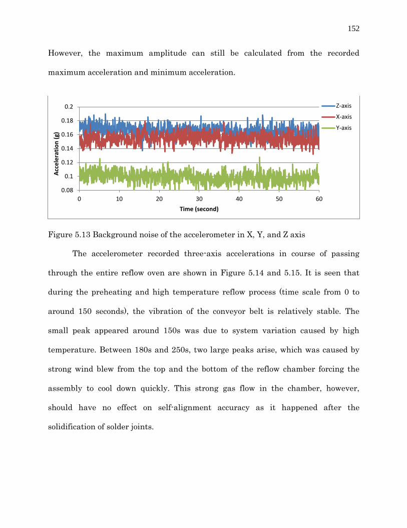
152
However, the maximum amplitude can still be calculated from the recorded
maximum acceleration and minimum acceleration.
Figure 5.13 Background noise of the accelerometer in X, Y, and Z axis
The accelerometer recorded three-axis accelerations in course of passing
through the entire reflow oven are shown in Figure 5.14 and 5.15. It is seen that
during the preheating and high temperature reflow process (time scale from 0 to
around 150 seconds), the vibration of the conveyor belt is relatively stable. The
small peak appeared around 150s was due to system variation caused by high
temperature. Between 180s and 250s, two large peaks arise, which was caused by
strong wind blew from the top and the bottom of the reflow chamber forcing the
assembly to cool down quickly. This strong gas flow in the chamber, however,
should have no effect on self-alignment accuracy as it happened after the
solidification of solder joints.
0.08
0.1
0.12
0.14
0.16
0.18
0.2
0 10 20 30 40 50 60
Acc
ele
rati
on
(g)
Time (second)
Z-axis
X-axis
Y-axis

153
Figure 5.14 Accelerometer recorded three-axis accelerations in course of passing
through the entire reflow oven
The data in Figure 5.14 were further zoomed in to measure acceleration
frequency and amplitude of the conveyor belt, as shown in Figure 5.15. The first
observation is that Y axis acceleration is a little bit larger than that of X and Z axis,
and all of them have amplitude in the range of 0.05-0.1g. Sudden mechanical shocks
happened occasionally, and such shock affects the motion of the conveyor belt in all
three directions. Apart from these large mechanical shocks, the dynamic vibrations
are relatively smooth and repeatable and can be approximately regarded as
periodical vibration. The measured vibration frequencies of the conveyor belt along
X, Y and Z axis are in the range of around 1.4-2 Hz, which are in low frequency
range. As a comparison, the acceleration amplitude that brings the current BGA
test vehicle into resonance is comparable to the vibration amplitude of the conveyor
belt (Figure 5.16). However, the around 2 Hz conveyor belt vibration frequency is

154
apart from the resonant frequency of the current BGA assembly. Therefore, the
tested reflow system is expected to exert no significant effect on the self-alignment
of the current BGA test vehicle if occasional sudden mechanical shocks were not
considered. Of course, it is difficult for us to draw any conclusion from a single
reflow oven characterized as above. Nevertheless, we have gained an insight into
the potential vibration effect on solder self-alignment.
-0.2
-0.1
0
0.1
0.2
0.3
0.4
0.5
0 5 10 15 20 25 30 35 40 45 50
Y-axis
-0.2
-0.1
0
0.1
0.2
0.3
0.4
0.5
0 5 10 15 20 25 30 35 40 45 50
X-axis

155
Figure 5.15 Accelerometer recorded vibration of the conveyor belt along X, Y, and Z
axis
Figure 5.16 Accelerometer recorded vibration of the hotplate along X, Y, and Z axis
that drives BGA test vehicle into resonance
5.6 Chapter Summary
In this chapter, the dynamic behavior of a BGA assembly reflowed under a
forced substrate vibration was investigated. Due to low dissipative force of the
-0.2
-0.1
0
0.1
0.2
0.3
0.4
0.5
0 5 10 15 20 25 30 35 40 45 50
Z-axis

156
molten solder joint, resonant oscillations between the chip and the substrate was
observed at around 12 Hz driving frequency for the specific configuration studied.
The maximum chip‟s oscillation amplitude could reach up to 100 µm for only several
microns‟ driving amplitude on the substrate. This resonant motion could be "frozen
in" during the solidification process of the solder joints and result in large post-
assembly misalignments. In order to reduce the adverse influence of such an
environmental vibration on self-alignment accuracy, several feasible methods were
proposed, including varying solder surface tension coefficient, solder joint aspect
ratio, chip mass, and the number of joint interconnections, in order to shift the
resonant frequency of the to-be-assembled device to a range that is different from
the frequency of environmental vibrations. Dynamic characterization of a real SMT
line indicates that the conveyor belt‟s vibration in X, Y and Z directions is in the
range of 1.4-2 Hz and may not have significant effect on the designed BGA test
vehicle, however, for any real applications, it is important to characterize the
frequency range of the manufacturing environment and make sure the resonant
frequencies of the assembly are far from the range.
It should be noted that we have not been able to study the vibration effect
on the flip-chip assembly. The resonant frequencies of flip-chip assemblies are
usually much higher than those of BGA assemblies. It is not unusual to have a flip-
chip assembly with resonant frequencies up to 100‟s or even 1000‟s of Hz. If the
vibration frequencies of a solder reflow oven or hot plate are usually around a few
Hz, it is possible that we can neglect the vibration effect on solder self-alignment.

157
CHAPTER 6 SUMMARY AND FUTURE WORK
6.1 Summary
In this dissertation, effects of different design and manufacturing factors on
self-alignment accuracy were studied through experimental and modeling studies.
Design guidelines were developed to improve the accuracy of the solder self-
alignment with respect to different configurations and variations. Specifically,
In Chapter 2, we developed a 6DOF solder self-alignment model based on a
force optimization algorithm to predict the alignment accuracy with input
manufacturing parameters and tolerances. We also experimentally verified the
model. The experimental results correlated with the model‟s predictions to be
within 3% for the lateral alignments and 2% for the standoff height. By using this
model, the effects of solder volume variation, solder volume distribution, as well as
chip mass on the post-assembly alignment accuracies were further investigated.
In Chapter 3, the 6DOF self-alignment model was used to explore design
widows for a flip-chip assembly with 1x12-arrayed VCSELs. To achieve the 50 µm
target chip standoff height, three pad/solder diameter combinations, 52 µm_pad/70
µm_sphere, 70 µm_pad/80 µm_sphere and 90 µm_pad/90 µm_sphere, were
evaluated. The worst case analysis was performed using the model to determine the
manufacturing tolerances of solder volume deviation/variation of the three
combinations. For an initial two-row pad design, solder spheres used for chip
bumping should have a diameter with a manufacturing tolerance within ± 0.8 µm to

158
achieve less than 2 µm height_Z variation, and this tolerance could be improved to ±
2 µm through a proposed ten-row new design. For most optoelectronic devices that
are small in size and low in mass, no calibration of solder surface tension coefficient
is needed. However, for the model to be valid for heavy BGA boards with mass
larger than 0.1 grams, solder‟s surface tension coefficient should be determined by
experiments. The 6DOF solder self-alignment model was proven to be a powerful
tool in the design of precision flip-chip optoelectronic modules by providing a
quantitative guideline on tolerances.
In Chapter 4, we concluded that insufficient wetting and solder voids during
formic acid-based reflow have significant influences on self-alignment accuracy.
Complete wetting of solder on bonding pads resulted in good alignments, while
incomplete wetting resulted in increased misalignments caused by nonsymmetrical
solder joints formed. In order to reduce the misalignment caused by incomplete
wetting, a large pitch between the bonding pads is preferable. Solder voids was
another undesired factor and it increased the standoff height variation of the
assembled unit. However, it imposed almost no impact on lateral alignments. Other
fabrication variations, e.g. bonding pads diameter manufacturing variations, only
accounted for less than ±1 µm misalignments. The 6DOF solder self-alignment
model developed in Chapter 2 was modified to model these factors and was further
used to develop design guidelines to minimize their effects. In addition to design,
these two undesirable factors can also be eliminated by increasing formic acid
concentration during the reflow process.

159
In Chapter 5, the dynamic behaviors of BGA assemblies reflowed under
forced substrate vibrations were investigated. We concluded that due to low
dissipative force of the molten solder, resonant oscillations between chip, i.e. BGA
board, and the substrate were observed at around 12 Hz driving frequency for the
specific test vehicle studied. The maximum oscillation amplitude could reach over
100 µm corresponding to driving amplitudes with only several microns. This
resonant motion could be "frozen in" during the solidification process of the joint,
resulting in large misalignments post-assembly. In order to reduce such an effect,
we recommended shifting the natural frequency of the self-assembled module to a
region that is far away from manufacturing vibration frequencies. We studied the
influences of solder surface tension coefficient, solder aspect ratio, chip mass, and
number of joint interconnections on the system‟s resonance frequencies. The results
showed that increasing joint number in the assembly was the most effective way to
change the resonant frequencies significantly. For any real applications, it is
important to characterize the frequency range of the manufacturing environment
and make sure the resonant frequencies of the assembly are far from the range. For
a specific solder reflow oven characterized, the vibration frequencies were in the
range of a few Hz. As a result, the abovementioned vibration effect on self-
alignments might be negligible. We did not study flip-chip assemblies due to the
limitations of the setup. Typically, the resonant frequency of a flip-chip assembly is
much higher that of a BGA. Since the vibration effect on BGA might be negligible,
we do not expect to see any major effect on flip-chip assembly.

160
A comprehensive solder self-alignment model has been developed; it is also
proven by experimental characterizations. This model is important to design
optoelectronic assemblies for precision solder self-alignments.
6.2 Future Work
Based on the works of this dissertation, we have identified new issues to be
considered in future studies. The recommendations for these studies are
summarized as follows:
6.2.1 Future Work on Investigating Static Factors Affecting Self-alignment
Accuracy
First of all, due to the limitations of Lin‟s regression model, the current self-
alignment model regards the top and bottom bonding pads on two parallel planes.
This provides reasonable results for fine pitch and small joint design since the chip‟s
rotation angles are very small compared to the form factor of the chip to be
considered. However, if the top bonding pad has a large inclination relative to the
bottom pad, as shown in Figure 6.1, the calculated restoring and normal reaction
forces would be inaccurate. Such a situation may be found in some BGA assemblies
where large solder joints are employed with large manufacturing variations. In
these cases, a new regression model calculating solder restoring and normal
reaction forces incorporating top pad inclination and misalignment needs to be
developed by simulating this configuration using the Surface Evolver.

161
In fact, it is desirable to integrate the Surface Evolver‟s computation with the
6 DOF self-alignment model. Such an integrated model will be able to
characterization very complicated solder self-aligned assemblies.
Figure 6.1 Illustration of a solder joint with parallel bonding pad pair and inclined
bonding pad pair
One possible solution to address insufficient wetting issue proposed in
chapter 4 is to have a smaller top bonding pad and a large bottom one, as shown in
Figure 6.2. By reducing the dimension of top bonding pad, solder wetting spread
area is greatly reduced and the effect of insufficient wetting may be reduced. In
addition, such a design may be able to generate larger restoring force than that
with the normal symmetric bonding pads, thus improving the capability of solder
self-aligning technology. As a matter of fact, such a nonsymmetrical bonding pad
design is not unusual in industrial practices. If our model has the capability to
process force optimization on such a design, we would be able to cover more
innovative design solutions. Therefore, it is desirable to develop a regression model
to calculate the resorting and normal reaction forces generated by a nonsymmetrical
bonding pad pair.

162
Figure 6.2 Illustration of a solder joint with large bottom bonding pad and small
top bonding pad
In addition, thermo-mechanical analysis is important to the chip-to-substrate
assembly. High temperature reflow would not only create large warpage on the
substrate and the chip, but also create large thermal stress between chip and
substrate through solid solder joints, inducing large misalignments. The situation
would become even worse with the adoption of lead-free solder materials (e.g. SAC)
since the reflow temperature has to be increased to 280 °C. Future self-alignment
model should be integrated with thermo-mechanical finite element model to cover
the effects associated with solid solder joints.
6.2.2 Future Work on Investigating Dynamic Factors Affecting Self-alignment
Accuracy
In Chapter 5, we have characterized the real vibration conditions on the
conveyor belt of an SMT reflow oven. Obviously the dynamic environments that a
BGA/optoelectronic module to be assembled is much more complicated than the
controlled vibration hotplate in experimental studies. And the model prediction
should be verified by a test vehicle going through the real manufacturing processes.
Unfortunately, due to limited access to these SMT manufacturing lines, we were not
163
able to run extensive experiments on a real SMT reflow oven. Future works should
include reflow the test vehicle through a real SMT line to verify the model, and
possibly identify other unexpected dynamic factors in the manufacturing line
affecting alignment accuracy.
Compared to the BGA assembly we investigated in Chapter 5, flip-chip
packaged optoelectronics usually composes chip and solder joints in much smaller
size. The small mass of the chip and large numbers of fine pitch solder joints in
optoelectronic packaging yield predicted resonant frequency in the range of
hundreds Hz. However, our initial attempts of using small-sized optoelectronic
packaging e.g. dummy VCSEL assembly as test vehicle failed to observe any
resonant behavior. We attribute this phenomenon to several possible reasons. First
of all, the camera and microscope we used for experiments are low speed and low
resolution and may not be able to identify high frequency and small amplitude
displacement between chip and substrate. Secondly, the parameters e.g. viscosity
and surface tension coefficient we used to predict theoretical resonant frequency of
the assembly were based on the liquid solder joint in pure metal state. However,
small solder spheres are prone to surface oxidation and their surface tension
coefficient and viscosity may deviate a lot due to the change of material
compositions. As a result, the real resonant frequency of the system would deviate
hundreds of Hz from theoretical predicted frequency and it is hard for us to scan the
whole frequency spectrum to identify it. What‟s more, if the effect of oxidation layer
is large enough, overdamping phenomenon may have to be considered, resulting in

164
totally different mechanisms between large-sized BGA and small-sized flip-chip
packaging. Therefore, more work needs to be done to understand the reflow process
difference between large-sized BGA and small-sized flip-chip packaging.
An extensive study on various BGA and flip-chip assemblies and reflow ovens
and hot plates is needed. For most of cases, we expect the effect to be negligible
though. If the vibration effect is important in some cases, the current model can be
improved further. Besides resonance frequency, solidification time of the solder joint
is also important in determining final alignment accuracy since whether the
resonant motion will be “locked in” or not depends on the comparison of
solidification time and resonant period. Is it possible to prolong solidification time of
solder material through a controlled reflow process to avoid such sudden “freeze in”?
Further studies should be performed to understand the solder solidification process
and integrate this process to the solder self-alignment model with molten solder
being solidified gradually in an environment with dynamic vibrations.

165
Bibliography
[1] Hideyuki Takahara, Optoelectronic Multichip Module Packaging Technologies
and Optical Input/Output Interface Chip-Level Packages for the Next Generation of
Hardware Systems, IEEE JOURNAL OF SELECTED TOPICS IN QUANTUM
ELECTRONICS, VOL. 9, NO. 2, MARCH/APRIL 2003, pp. 443-451.
[2] Christopher Quirke, Gilbert Lecarpentier, High Accuracy Flip-Chip Assembly of
MOEMS, Iot'l Symposium on Electronic Materials and Packaging, 2002.
[3] Iezeki, el, S., Soshea, e.A., O‟Keefe, M.f., and Snowden, C.M., “Application of
Silicon-Glass Technology to Microwave Photonic Multichip Modules”, Proceedings of
Interpack, 1997, pp. 759-764.
[4] L. F. Miller, “Controlled Collapse of Reflow Chip Joining,” IBMJ. Res.
Develop.,Vol. 13, 1969, pp. 239-250.
[5] Lee, Y.C. and Basavanhally N.R., "Overview: Solder Engineering For
Optoelectronic packaging" JOM, June. 1994, pp. 46-50.
[6] Itoh M., Sasaki, J., Uda, A., Yoneda, I., Honmou, H., Fukushima, K., "Use of
AuSn Solder Bumps in Three-dimensional Passive Aligned Packaging of LD/PD
Arrays on Si Optical Benches", Proc. of 46th ECTC, 1996, pp. 1-7.
[7] Hayashi T., "An Innovative Bonding Techniques for Optical Chips Using Solder
Bumps That Eliminate Chip Position Adjustments" IEEE Trans. CHMT, Vol. 15,
No. 2, 1992, pp. 225-230.
[8] Bingzhi Su, M. Gershovich and Y. C. Lee, “Gas Flow Effects on Precision Solder
Self-Alignment,” IEEE Transactions on Components, Packaging and Manufacturing
Tech., Part C, Vol. 20, No. 4, October 1997, pp. 1-7.
[9] Kuo-Ning Chiang and Chang-An Yuan, An Overview of Solder Bump Shape
Prediction Algorithms with Validations, IEEE TRANSACTIONS ON ADVANCED
PACKAGING, VOL. 24, NO. 2, May 2001, pp. 158-162.
[10] N. van Veen, Analytical Derivation of the Self-Alignment Motion of Flip Chip
Soldered Components, Transactions of the ASME, Vol. 121, June 1999, pp. 116-121.

166
[11] J.M. Kim, Y.E. Shin, K. Fujimoto, Dynamic modeling for resin self-alignment
mechanism Microelectronics Reliability, 44 (2004) 983-992.
[12] Goldmann,L.S., ”Geometric optimization of controlled collapse
interconnections”, IBM Journal of Research and Development, May 1969, pp.25 1-
265.
[13] S. M. Heinrich, M. Schaefer, S. A. Schroeder, and P. S. Lee, “Prediction of
solder joint geometries in array-type interconnects,” ASME J. Electron.Packag., vol.
118, 1996, pp. 114-121.
[14] Patra, S. K. and Lee, Y. C.,”Quasi-Static Modeling of Self-Alignment
Mechanism in Flip-Chip Soldering Process, Part I: Single Joint”, ASME Journal of
Electronic Packaging, Dec. 1991, pp. 337-342.
[15] S. K. Patra, Wei Lin, and Y. C. Lee, CAD OF SOLDER JOINTS FOR SELF-
ALIGNED ASSEMBLIES.
[16] Sidharth, Richard Blish and Devendra Natekar, Solder Joint Shape and
Standoff Height Prediction and Integration with FEA-Based Methodology for
Reliability Evaluation, 2002 Electronic Comaonents and Technolouv Confermm, pp.
1739-1744.
[17] G.K. Mui, X.H. Wu, K.X. Hu, C.P. Yeh and K. Wyatt, “Solder Joint Formation
Simulation and Finite Element Analysis”, Roc of ECTC, 1997, pp. 436-443.
[18] Jeffery C. C. LO, S. W. Ricky LEE, Henry H. L. Wu and Jimmy K. S. Lam,
Determination of Solder Bump Stand-Off Height in a Flip-Chip Sub-Mount for
Micro-Opto-Electro-Mechanical System (MOEMS) Packaging Applications, 2008
Electronic Components and Technology Conference, pp. 1887-1892.
[19] Lin W., Patra S.K. and Lee Y.C., "Design of Solder Joint For Self-Aligned
Optoelectronic Assembly" IEEE Trans. CHMT, Vol. 18, No. 3, 1995b, pp. 543-551.
[20] Brakke, K. A., “The Surface Evolver,” Experimental Mathematics, Vol. 1, pp.
141-165.

167
[21] Edge C., Ash R.M., Jones C.G. and Goodwin M.J., "Flip-Chip Solder Bond
Mounting of Laser Diodes" Electronic Letters, Vol 27, No. 6, 1991, pp. 499-501.
[22] Itoh M., Naganori T., Kohashi H., Kaneko H., Honmou H., Watanable I., Uji T.
and FujiWara M., "Compact Multi-Channel LED/PD Array Modules Using New
Assembly Techniques for Hundred Mb/s/ch Parallel Optical Transmission"
Proceedings of the 41st ECTC, 1991, pp. 475-478.
[23] Tsunetsugu H., Katsura K., Hayashi T.,Ishitsuka F. and Hata S., "A New
Packaging Technology Using Microsolder Bumps for High-Speed Photoreceivers"
IEEE Trans. CHMT, Vol. 15, No.4, 1992, pp.578-582.
[24] Lin, W., Lee Y.C. and Johnson K.M., "Study of Soldering for VLSI/FLC Spatial
Light Modulators" Proceeding of the 43rd ECTC, 1993, pp. 491-497.
[25] T. H. Ju, W. Lin, Y. C. Lee, D. J. McKnight, and K. M. Johnson, Packaging of a
128 by 128 Liquid-Crystal-on-Silicon Spatial Light Modulator Using Self-pulling
Soldering, IEEE PHOTONICS TECHNOLOGY LETTERS, VOL. 1, NO. 9,
SEPTEMBER 1995, pp. 1010-1012.
[26] Sasaki J. Honmou, H., Itoh, M., Uda, A., Torikai, T., "Self-aligned assembly
technology for laser diode modules using stripe-type AuSn solder bump flip-chip
bonding", Proc. of LEOS'95, 1995, pp. 234-235.
[27] Dautartas M.F., Benzoni A.M., Broutin S.L., Coucoulas A. Moser D.T., Wong Y-
H and Wong Y.M., "Optical Performance of Low-Cost Self-aligned MCM-d Based
Optical Data Links" Proceeding of the 45th ECTC, 1995a, pp. 1254-1262.
[28] Patrick J. Nasiatka and Zaheed S. Karim, Determination of Optimal Solder
Volume for Precision Self-Alignment of BGA using Flip-Chip Bonding, pp.6-9.
[29] Hideki Tsunetsugu, Tsuyoshi Hayashi, and Kohsuke Katsura, Micro-alignment
Technique using 26-pn Diameter Microsolder Bumps and its Shear Strength,
Electronic Manufacturing technology symposium, proceedings of 1995 Japan
International, 18th IEEE/CPMT International, pp. 52-55.

168
[30] Pusarla, P., and Christou, A., “Solder Bonding Alignment of Microlens in
Hybrid Receiver for Free Space Optical Interconnections”, Proceedings of 46th
ECTC, 1996, pp. 42-47.
[31] Morozova, N., Liew, L.A., Zhang, W., Irwin, R., Su, B, and Lee, Y.C.,
“Controlled Solder Self-alignment Sequence for an Optoelectronic Module without
Mechanical Stop," Proceedings of 46th ECTC. 1996, pp. 1188-1193.
[32] J. F. Kuhmann, H.-J. Hensel, D. Pech, P. Harde, H.-G. Bach, Self-Aligned,
Fluxless Flip-Chip Bonding Technology for Photonic Devices, 1996 Electronic
Components and Technology Conference.
[33] Tsuyoshi Hayashi and Hideki Tsunetsugu, Optical Module with MU Connector
Interface Using Self-alignment Technique by Solder-bump Chip Bonding 1996
Electronic Components and Technology Conference, pp.13-19.
[34] Christine Kallmayer, Hermann Oppermann, Gunter Engelmann, Elke Zakel,
Herbert reichl, Self-Aligning Flip-Chip Asse utectic Gold/Tin Solder in different
atmospheres 1996 lEEE1CPMT Int'l Electronics Manufacturing Technology
Symposium, pp. 18-25.
[35] K. C. Hung, Y. C. Chan, P. L. Tu, H. C. Ong, D. P. Webb, and J. K. L. Lai,
Study of Self-Alignment of µBGA Packages, IEEE TRANSACTIONS ON
ADVANCED PACKAGING, VOL. 23, NO. 4, NOVEMBER 2000, pp. 631-636.
[36] Hermann Oppermann, Matthias Hutter, Gunter Engelmann, Herbert Reichl,
Passive alignment flip chip assembly using surface tension of liquid solder and
micromechanical stops, Reliability, Packaging, Testing, and Characterization of
MEMS/MOEMS IV (Proceedings Volume) Proceedings Vol. 5716, 2005, pp.19-25.
[37] J. Sasaki et. al., “Multiple-Chip Precise Self-Aligned Assembly for Hybrid
Integrated Optical Modules using Au-Sn Solder Bumps”, IEEE Transacrions on
Advanced Pachging, vol. 24, no. 4 , 2001, pp. 569-575.
[38] W. Salalha, E. Zussman, P. Z. Bar-Yoseph, Investigation of Flip-Chip Bonding
for MEMS Applications, Transactions of the ASME, Vol. 126, March 2004, pp. 48-
51.

169
[39] Lee S.H., Joo G.C., Park K.S., Kim H.M., Kim D.G. and Park H.M., "Optical
DeviceModule Packages for Subscriber Incorporating Passive Alignment
Techniques", Proceeding ofthe 45th ECTC, 1995, pp. 841-844.
[40] DO H. AHN, JIHYE LEE, CHOONG D. YOO, and YONG-SEOG,KIM,
Influence of Pad Shape on Self-Alignment in Electronic Packaging, Journal of
ELECTRONIC MATERIALS, Vol. 35, No. 3, 2006, pp. 411-415.
[41] SCOTT E. DEERING and JULIAN SZEKELY, Mathematical Modeling of
Alternative Pad Designs in Flip-Chip Soldering Processes, Journal of Electronic
Materials, Vol. 23, No. 12, 1994, pp.1325-1334.
[42] Wei Lin and Y. C. Lee, Study of Fluxless Soldering Using Formic Acid Vapor,
IEEE TRANSACTIONS ON ADVANCED PACKAGING, VOL. 22, NO. 4, November
1999, pp. 592-601.
[43] K. C. Hung, Y. C. Chan, P. L. Tu, H. C. Ong, D. P. Webb, and J. K. L. Lai,
Study of Self-Alignment of µBGA Packages, IEEE TRANSACTIONS ON
ADVANCED PACKAGING, VOL. 23, NO. 4, November 2000, pp. 631-636.
[44] Landry M, Patra SK, Lee YC. Experiment and modeling of the self-alignment
mechanism in flip-chip soldering. Manufact Processes Mater Challenges,
Microelectron Package ASME Vol 131, 1991, pp. 49-56.
[45] Ruijun Chen et. al., Flip Chip Self-alignment Mechanism and Modeling,
International Symposium on Advanced Packaging Materials, 2000, pp. 158-164.
[46] Jong-Ming, Kim, et.al.Highly precise positioning method by pull-up model self-
alignment process using liquid surface tension, Quarterly Journal of Japan Welding
Society, Vol.20, No.3, pp. 346-354 (2002), 346-354.
[47] Hua L, Bailey C, Dynamic Analysis of Flip-Chip Self-Alignment, IEEE
Transaction on Advanced Packaging, August 2005, pp. 475-480.
[48] Cheng Lin et.al., Numerical studies on micropart self-alignment using surface
tension forces, Microfluid Nanofluid (2009) Vol. 6, pp. 63-75.

170
[49] Julien Sylvestre, Vibrations in the Flip-Chip Soldering Process, IEEE
TRANSACTIONS ON COMPONENTS, PACKAGING AND MANUFACTURING
TECHNOLOGY, VOL. 1, NO. 6, June 2011, pp. 904-911.
[50] M. Rayasam, and G. Subbarayan, “A three-dimensional solder shape model
incorporating top pad inclination and misalignment,” ASME Journal of electronic
packaging, vol.128, 2006, pp. 291-293.
[51] D. Josell, W.E. Wallace, J.A. Warren, D. Wheeler, and A.C Powell IV,
“Misaligned flip-chip solder Joints: prediction and experimental determination of
force-displacement curves,” ASME Journal of electronic packaging, vol.124, 2002, pp.
227-233.
[52] S.E. Deering and J. Szekely, “Mathematical modeling of alternative pad
designs in flip-chip soldering processes,” Journal of Electronic materials, vol.23,
no.12, 1994, pp.1325-1333.
[53] Y. Zhang, R.Z. Zhao, D.L. Harries, and R. W. Johnson, “A computational study
on solder bump geometry, normal, restoring, and fillet forces during solder reflow in
the presence of liquefied underfill,” IEEE transactions on electronics packaging
manufacturing, vol.25, no.4, pp.308-317, October, 2002.
[54] Lu, J. C., Busch, S. C., and Baldwin, D. F., "Solder Wetting in a Wafer-Level
Flip Chip Assembly," IEEE Trans. Electron. Pack. Manuf., 24(3), 2001, pp. 372-377.
[55] Qi, Y., Zbrzezny, A. R., Agia, M., Laml, R., Ghorbani, H. R., Snugovsky, P.,
Perovic, D. D., and Spelt, J. K., "Accelerated Thermal Fatigue of Lead-free Solder
Joints as A Function of Reflow Cooling Rate," J. Electron. Mater, 33(12), 2004, pp.
1497-1506.
[56] J. A. Tatum, “Packaging flexibility propels VCSELs beyond
telecommunications,” Laser Focus World, vol. 36, no. 4, Apr. 2000, pp. 131-136.
[57] J. J. Liu, K. A. Olver, M. T. Lara, T. Taylor, W. Chang, and S. Horst, “High yield
flip-chip bonding and packaging of low-threshold VCSEL arrays on sapphire
substrates,” IEEE Trans. Compon. Packag. Technol., vol. 26, no. 3, Sep. 2003, pp.
548-553.

171
[58] Y. Ishii, N. Tanaka, T. Sakamoto, and H. Takahara, “Fully SMT-compatible
optical-I/O package with microlens array interface,” J. Lightw. Technol., vol. 21, no.
1, Jan. 2003, pp. 275-280.
[59] T. Chen, A. K. Nallani, J. B. Lee, D. J. Hayes, and D. B. Wallace, “Inkjet
printing for optical/electrical Interfacing of VCSEL and PD arrays,” in Proc. IMAPS
Int. Symp. Microelectronics Processing, Boston, MA, 2003, pp. 864-868.
[60] K.-M. Chu, J.-S. Lee, H. S. Cho, B. S. Rho, H.-H. Park, and D. Y. Jeon,
“Characteristics of indium bump for flip-chip bonding used in polymeric-waveguide-
integrated optical interconnection systems,” Jpn. J.Appl. Phys., vol. 43, no. 8B, 2004,
pp. 5922-5927.
[61] S. H. Hall, W. L. Walters, L. F. Mattson, G. J. Fokken, and B. K. Gilbert,
“VCSEL electrical packaging analysis and design guidelines for multi-GHz
applications,” IEEE Trans. Compon., Packag., Manuf. Technol. B, vol. 20, no. 3, Aug.
1997, pp. 191-201.
[62] G. J. Fokken, W. L. Walters, L. F. Mattson, and B. K. Gilbert, “Low-cost, multi-
Ghz electrical packaging for serial optoelectronic links utilizing vertical cavity
surface emitting lasers,” IEEE Trans. Adv. Packag., vol. 23, no. 1, Feb. 2000, pp. 42-
54.
[63] Y. C. Lee, S. E. Swirhun, W. S. Fu, T. A. Keyser, J. L. Jewell, and W. E. Quinn,
“Thermal management of VCSEL-based optoelectronic modules,” IEEE Trans.
Compon., Packag., Manuf. Technol. B, vol. 19, no. 3, Aug. 1996, pp. 540–547.
[64] S. Kawai, “Parallel micro-optics for interconnections based on VCSEL arrays
and their Jisso technologies,” Opt. Eng., vol. 43, no. 5, May 2004, pp. 1018–1021.
[65] Ning-Cheng Lee, Reflow Soldering Processes and Troubleshooting: SMT, BGA,
CSP, and Flip Chip Technologies, Elsevier Science, Oxford, United Kingdom, 2001.
pp. 181-182.
[66] Thomas Siewert, Stephen Liu, David R. Smith, and Juan Carlos Madeni.
Database for Solder Properties with Emphasis on New Lead-free Solders, Properties
of Lead-Free Solders, Release 4.0, National Institute of Standards and Technology
& Colorado School of Mines, Colorado, February 11, 2002.

172
[67] Nguyen, L., Walberg, R., Zhou, L., and Koh, T., "Board Level Reliability of
Components with Matte Tin Lead Finish," ECTC, 2003, pp. 346-352.
[68]Guo-Wei Xiao, Jing-Feng Gong, Yau, E.W.C., Chan, P.C.H., Lee, R.S.W. , Yuen,
M.M.F., "Optimization of electroplating, stencil printing, ball placement solder,
bumping flip-chip process technologies," Electronic Components and Technology
Conference, 2003. Proceedings. 53rd, pp. 1850-1855.
[69] Kallmayer, C., Oppermann, H., Engelmann, G., Zakel, E., and Reichl, H., "Self-
Alignning Flip-Chip Assembly Using Eutectic Gold/Tin Solder in Different
Atmosphere," Nineteenth IEEE/CPMT Int. Electron. Manuf. Technol. Symp., 1996,
pp. 18-25.
[70] S. V. Sattiraju, B. Dang, R. W. Johnson, Y. Li, J. S. Smith and M. J. Bozack,
"Wetting Characteristics of Pb-free Solder Alloys and PWB Finishes," IEEE Trans.
Electron. Packag. Manuf., Vol 25, 2002, pp. 168-184.
[71] Evans, John W, "A Guide to Lead-free Solders. Physical Metallurgy and
Reliability," Springer, 1st Edition, 2007, pp. 6-7.
[72] Raiyo Aspandiar, Voids in Solder Joints, September 21th 2005 SMTA Northwest
Chapter Meeting
[73] Ronald L. Panton et. al. Simulation of Void Growth in Molten Solder Bumps,
Journal of Electronic Packaging, SEPTEMBER 2003, Vol. 125, pp.329-334
[74] Lakhi Goenka et.al., Void Formation in FlipChip Solder Bumps -- I'art I, 1995
lEEE1CPMT Int'l Electronics Manufacturing Technology Symposium
[75] Lakhi Goenka et.al., Void Formation in Flip Chip Solder Bumps -- Part I1, 1996
IEEUCPMT Int'l Electronics Manufacturing Technology Symposium
[76] Weicheng Lin, The Void-free Reflow Soldering of BGA with Vacuum, Electronic
Packaging Technology, 2007. ICEPT 2007.

173
[77] Zhao Zhendong, et.al., Moisture Absorption and Void Growing Effects on
Failure of Electronic Packaging, 2008 International Conference on Electronic
Packaging Technology & High Density Packaging
[78] Daijiao Wang, Experimental Study of Void Formation in Eutectic and Lead-
Free Solder Bumps of Flip-Chip Assemblies, Journal of Electronic Packaging,
SEPTEMBER 2006, Vol. 128 , pp. 202-207.
[79] Youmin Yu, Effects of Reflow Atmosphere on Solder Void and Wire Bond
Performances in a PQFN Package, Thermal and Thermomechanical Phenomena in
Electronic Systems, 2008. ITHERM 2008. 11th Intersociety Conference