experiment 1 realization of basic logic gates using
TRANSCRIPT

ANALOG & DIGITAL ELECTRONICES LAB MANUAL (CS252)
CHALAPATHI INSTITUTE OF ENGG & TECHNOLOGY Page 1
EXPERIMENT 1
REALIZATION OF BASIC LOGIC GATES USING UNIVERSAL
GATES
AIM To construct BASIC logic gates AND, OR, NOT using NAND gate and verify
their truth tables.
APPARATUS
1. IC’s 7400(NAND) 7402(NOR)
2. General Purpose Digital Trainer
3. Connecting wires.
Circuit Diagrams
Truth Table
Truth Table

ANALOG & DIGITAL ELECTRONICES LAB MANUAL (CS252)
CHALAPATHI INSTITUTE OF ENGG & TECHNOLOGY Page 2
THEORY
AND
A multi-input circuit in which the output is 1 only if all inputs are 1.The
symbolic representation of the AND gate is shown in Fig.
Truth Table
Truth Table
Truth Table
ANALOG & DIGITAL ELECTRONICES LAB MANUAL (CS252)
CHALAPATHI INSTITUTE OF ENGG & TECHNOLOGY Page 3
OR
A multi-input circuit in which the output is 1 when any input is 1. The
symbolic representation of the OR gate is shown in Fig. 1, and the output
is 1 when the input is 0. The symbolic representation of an inverter is
shown in Fig
NAND
AND followed by INVERT. The symbolic representation of the NAND gate
NOR
OR followed by INVERT as shown in Fig
EX-OR
The output of the Exclusive –OR gate, is 0 when it‟s two inputs are the
same and its output is 1 when its two inputs are different.
PROCEDURE
1. Connect the logic gates as shown in the diagrams.
2. Feed the logic signals 0 or 1 from the logic input switches in different
combinations at the inputs A & B.
3. Monitor the output using logic output LED indicators.
4. Repeat steps 1 to 3 for NOT, AND, OR, EX - OR & EX-NOR operations
and compare the outputs with the truth tables.
PRECAUTIONS
1. All the connections should be made properly.
2. IC should not be reversed.
RESULT Different logic gates are constructed using NAND gates and their truth
tables are verified.
ANALOG & DIGITAL ELECTRONICES LAB MANUAL (CS252)
CHALAPATHI INSTITUTE OF ENGG & TECHNOLOGY Page 4
Viva Questions
1. Why NAND & NOR gates are called universal gates?
2. Realize the EX - OR gates using minimum number of NAND gates?
3. Give the truth table for EX-NOR (EX-OR+NOT) and realize using NAND
gates
4. Realize the given logic function using NAND gates?
f = ABC + ABC + ABC

ANALOG & DIGITAL ELECTRONICES LAB MANUAL (CS252)
CHALAPATHI INSTITUTE OF ENGG & TECHNOLOGY Page 5
EXPERIMENT 2
DESIGN AND CONSTRUCT HALF-ADDER AND FULL-ADDER
CIRCUITS AND VERIFY THE TRUTH TABLES USING LOGIC
GATES
AIM
To design and construct Half-adder, Full-adder, Half-subtractor, Full-
subtractor and verify the truth tables.
APPARATUS
1. IC’s - 7486(X-OR), 7432(OR), 7408(AND), 7404 (NOT)
2. General Purpose Digital Trainer
3. Connecting wires.
Circuit Diagrams

ANALOG & DIGITAL ELECTRONICES LAB MANUAL (CS252)
CHALAPATHI INSTITUTE OF ENGG & TECHNOLOGY Page 6
THEORY
HALF ADDER
Half adder is a combinational logic circuit with two inputs and two
outputs. The half adder circuit is designed to add two single bit binary
numbers A and B. It is the basic building block for addition of two single
bit numbers. This circuit has two outputs CARRY and SUM.
Truth Table

ANALOG & DIGITAL ELECTRONICES LAB MANUAL (CS252)
CHALAPATHI INSTITUTE OF ENGG & TECHNOLOGY Page 7
Sum =A ⊕ B
Carry = A B
FULL ADDER
Full adder is a combinational logic circuit with three inputs and two outputs.
Full adder is developed to overcome the drawback of HALF ADDER circuit.
It can add two one bit numbers A and B. The full adder has three inputs A, B,
and CARRY in,the circuit has two outputs CARRY out and SUM.
Sum = (A⊕B) ⊕ Cin
Carry = AB + Cin (A⊕B)
HALF SUBTRACTOR
Subtracting a single-bit binary value B from another A (i.e. A -B) produces
a difference bit D and a borrow out bit B-out. This operation is called half
subtraction and the circuit to realize it is called a half subtractor. The
Boolean functions describing the half- Subtractor are
Sum =A ⊕B
Carry = A’ B
FULL SUBTRACTOR
Subtracting two single-bit binary values, B, Cin from a single-bit value A
produces a difference bit D and a borrow out Br bit. This is called full
subtraction. The Boolean functions describing the full-subtractor are
Difference = (A ⊕ B) ⊕Cin
Borrow = A’B + A’(Cin) + B(Cin)
PROCEDURE
1. Verify the gates.
2. Make the connections as per the circuit diagram.
3. Switch on VCC and apply various combinations of input according to

ANALOG & DIGITAL ELECTRONICES LAB MANUAL (CS252)
CHALAPATHI INSTITUTE OF ENGG & TECHNOLOGY Page 8
truth table.
4. Note down the output readings for half/full adder and half/full
subtractor, Sum/difference and the carry/borrow bit for different
combinations of inputs verify their truth tables.
PRECAUTIONS
1. All the connections should be made properly.
2. IC should not be reversed.
RESULT
Combinational logic circuits like Half-adder, Full-adder, Half Subtractor,
and Full Subtractor are constructed and truth tables are verified.
VIVA QUESTIONS
1. Describe the difference between half-adder and full-adder.
2. Describe the difference between half - subtractor and full- subtractor.

ANALOG & DIGITAL ELECTRONICES LAB MANUAL (CS252)
CHALAPATHI INSTITUTE OF ENGG & TECHNOLOGY Page 9
EXPERIMENT 3
DESIGN AND IMPLEMENT A 4-BIT ADDER/SUBTRACTOR
USING IC 7483
AIM
To design and construct of 4-bit parallel adder/Subtractor using IC 7483
and verify their truth tables.
APPARETUS
1. IC’s -7483
2. General Purpose Digital Trainer
3. Connecting wires
Circuit diagrams
Figure 3.1 4 bit parallel adder/subtract or using 2”s complement
subtraction
Observation Table A3
A2
A1
A0
B3
B2
B1
B0
C4
S3
S2
S1
S0
0 0 0 1 0 0 1 0 0 0 0 1 1 0 1 0 1 1 0 1 1 1 1 0 0 0 1 0 1 0 1 0 1 0 1 0 1 0 0 1 1 1 1 1 1 1 1 1 1 1 1 0 0 1 1 1 0 0 1 1 0 1 0 1 0

ANALOG & DIGITAL ELECTRONICES LAB MANUAL (CS252)
CHALAPATHI INSTITUTE OF ENGG & TECHNOLOGY Page 10
PIN DIAGRAM FOR 7483
PROCEDURE
1. Connect the circuit as shown in fig. Feed the 4-bit binary words A0,
A1, A2, A3 and B0, B1, B2, B3 from the logic input switches.
2. Connect carry in from pin no.13 to ground so that carry input (CY1)
will be logic ‘0’state.
3. Connect S0, S1, S2, S3 and carry out (CY0) from pin nos. 9, 6, 2, 15
and 14 to the output display.
4. Verify truth tables for different combinations of inputs.
PRECAUTIONS
1. All the connections should be made properly.
2. IC should not be reversed.
RESULT
Binary 4 bit full adder is studied and verified
VIVA QUESTIONS
1. What is parallel adder?
2. What is parallel subtractor?

ANALOG & DIGITAL ELECTRONICES LAB MANUAL (CS252)
CHALAPATHI INSTITUTE OF ENGG & TECHNOLOGY Page 11
EXPERIMENT 4
DESIGN AND IMPLEMENT MULTIPLEXER AND
DEMULTIPLEXER USING LOGIC GATES
AIM
To design and construct of Multiplexer and Demultiplexer using logic gates
and verify their truth tables.
APPARATUS
1. IC- 7404,7411,7432,7408
2. General Purpose Digital Trainer
3. Connecting wires
CIRCUIT DIAGRAMS
Figure 4.1 A labeled 4:1 multiplexer circuit with IC numbers and the
corresponding pin
ANALOG & DIGITAL ELECTRONICES LAB MANUAL (CS252)
CHALAPATHI INSTITUTE OF ENGG & TECHNOLOGY Page 12
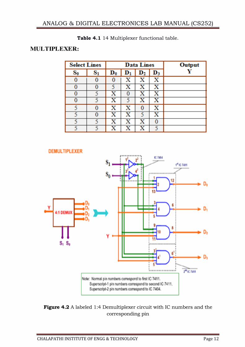
Table 4.1 14 Multiplexer functional table.
Figure 5.2 A labeled 14 demultiplexer circuit with IC numbers and the
corresponding pin numbers.
Figure 4.2 A labeled 1:4 Demultiplexer circuit with IC numbers and the
corresponding pin

ANALOG & DIGITAL ELECTRONICES LAB MANUAL (CS252)
CHALAPATHI INSTITUTE OF ENGG & TECHNOLOGY Page 13
Table 4.2 : 1:4 Demultiplexer functional table
THEORY
MULTIPLEXER
A multiplexer (MUX) is a device that accepts data from one of many input
sources for transmission over a common shared line. To achieve this MUX
has several data lines and a single output along with data –select inputs,
which permit digital data on any of the inputs to be switched to the output
line. The selection lines decide the number of inputs lines of particular
multiplexer. If the number of n inputs lines is equals to 2m, then m select
lines are required to select one of the n input line.
DEMULTIPLEXER
A demultiplexer is a device, that has one input and multiple output lines
which is used to send a signal to one of the various devices. The most
prominent distinction between a multiplexer and demultiplexer is that a
multiplexer takes two or a lot of signals and encodes them on a wire,
whereas a demultiplexer reverses what the multiplexer does.

ANALOG & DIGITAL ELECTRONICES LAB MANUAL (CS252)
CHALAPATHI INSTITUTE OF ENGG & TECHNOLOGY Page 14
PROCEDURE
1. Connect the logic circuit for De-MUX as shown in Figure. 5.2 using
ICs 7404, and 7411.
2. Connect 5V to V DD pin and 0V to GND pin of all ICs.
3. Connect four LEDs at the four outputs of the demultiplexer. Use
current limiting resistor in series with each LED. Proper LED
connection is illustrated in Figure 5.2.
4. Apply inputs to select lines and E according to the demultiplexer
function table, and complete Table
5. A 0V input results in all LEDs being switched off; a 5V input results
in one LED glowing on the output line selected by the two select
lines.
PRECAUTIONS
1. All the connections should be made properly.
RESULT
Multiplexer and Demultiplexer are constructed and the truth tables are
verified
VIVA QUESTION
1. What is the difference between multiplexer and decoder

ANALOG & DIGITAL ELECTRONICES LAB MANUAL (CS252)
CHALAPATHI INSTITUTE OF ENGG & TECHNOLOGY Page 15
EXPERIMENT 5
IMPELEMENTATION OF SR, T-Type, D-Type and JK FLIP
FLOPS
AIM
To design and construct basic flip-flops R-S, J-K, D and T flip-flops using
gates and verify their truth tables.
APPARATUS
1. IC’s- 7404, 7410, 7400
2. General Purpose Digital Trainer
3. Connecting wires
CIRCUIT DIAGRAM
SR FLIP-FLOP
S R Q
0 0 NO Change
0 1 0
1 0 1
1 1 Forbidden
Truth Table

ANALOG & DIGITAL ELECTRONICES LAB MANUAL (CS252)
CHALAPATHI INSTITUTE OF ENGG & TECHNOLOGY Page 16
JK FLIP-FLOP
T FLIP-FLOP
J K Q
0 0 NO Change
0 1 0
1 0 1
1 1 Race around
T Q Qn+1
0 0 0
0 1 1
1 0 1
1 1 0
Truth Table
Truth Table

ANALOG & DIGITAL ELECTRONICES LAB MANUAL (CS252)
CHALAPATHI INSTITUTE OF ENGG & TECHNOLOGY Page 17
D FLIP-FLOP THEORY Flip-Flops are the basic building blocks of sequential circuits. A flip-flop is a
binary cell which can store a bit of information. A basic function of flip-flop
is storage, which means memory. A flip-flop (FF) is capable of storing 1 (one)
bit of binary data. It has two stable states either ‟1‟ or „0‟. A flip-flop
maintains any one of the two stable states which can be treated as zero or
one depending on presence and absence of output signals. A flip-flop circuit
has two outputs, one for the normal value and other for the complement
value of the bit stored in it.
PROCEDURE
1. Connect the Flip-flop circuits as shown above.
2. Apply different combinations of inputs and observe the outputs
PRECAUTIONS
1. All the connections should be made properly.
D Q Qn+1
0 0 0
0 1 0
1 0 1
1 1 1
Truth Table

ANALOG & DIGITAL ELECTRONICES LAB MANUAL (CS252)
CHALAPATHI INSTITUTE OF ENGG & TECHNOLOGY Page 18
RESULT
Different Flip-flops are constructed and their truth tables are verified.
VIVA QUESTIONS
1. Modify SR flip-flop to form D flip-flop. Thus write D flip-flop truth
table.
2. Modify JK flip-flop to form T flip-flop. Thus write T flip-flop truth table.
3. Write characteristic equations for SR flip-flop and JK flip-flop.
4. What is the difference between a flip-flop and a latch?
5. List four Basic Flip-flop applications?

ANALOG & DIGITAL ELECTRONICES LAB MANUAL (CS252)
CHALAPATHI INSTITUTE OF ENGG & TECHNOLOGY Page 19
EXPERIMENT 6
DESIGN AND VERIFY 4 BIT RIPPLE COUNTER AND MOD-10
RIPPLE COUNTER
AIM To design and verify 4 bit ripple counter mod 10 ripple counter.
APPARATUS
1. IC’s -7476, 7400
2. General Purpose Digital Trainer
3. Connecting wires
CIRCUIT DIAGRAM FOR 4 BIT RIPPLE COUNTER
Figure 6.1 circuit diagram for 4 bit ripple counter:

ANALOG & DIGITAL ELECTRONICES LAB MANUAL (CS252)
CHALAPATHI INSTITUTE OF ENGG & TECHNOLOGY Page 20
TRUTH TABLE:
CLK QA QB QC QD
0 0 0 0 0
1 1 0 0 0
2 0 1 0 0
3 1 1 0 0
4 0 0 1 0
5 1 0 1 0
6 0 1 1 0
7 1 1 1 0
8 0 0 0 1
9 1 0 0 1
10 0 1 0 1
11 1 1 0 1
12 0 0 1 1
13 1 0 1 1
14 0 1 1 1
15 1 1 1 1
CIRCUIT DIAGRAM FOR MOD - 10 RIPPLE COUNTER
Figure 6.2 circuit diagram for mod - 10 ripple counter

ANALOG & DIGITAL ELECTRONICES LAB MANUAL (CS252)
CHALAPATHI INSTITUTE OF ENGG & TECHNOLOGY Page 21
TRUTH TABLE
CLK QA QB QC QD
0 0 0 0 0
1 1 0 0 0
2 0 1 0 0
3 1 1 0 0
4 0 0 1 0
5 1 0 1 0
6 0 1 1 0
7 1 1 1 0
8 0 0 0 1
9 1 0 0 1
10 0 0 0 0
PIN DIAGRAM
ANALOG & DIGITAL ELECTRONICES LAB MANUAL (CS252)
CHALAPATHI INSTITUTE OF ENGG & TECHNOLOGY Page 22
THEORY
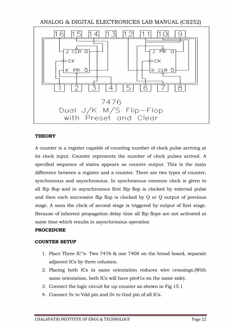
A counter is a register capable of counting number of clock pulse arriving at
its clock input. Counter represents the number of clock pulses arrived. A
specified sequence of states appears as counter output. This is the main
difference between a register and a counter. There are two types of counter,
synchronous and asynchronous. In synchronous common clock is given to
all flip flop and in asynchronous first flip flop is clocked by external pulse
and then each successive flip flop is clocked by Q or Q output of previous
stage. A soon the clock of second stage is triggered by output of first stage.
Because of inherent propagation delay time all flip flops are not activated at
same time which results in asynchronous operation
PROCEDURE
COUNTER SETUP
1. Place Three IC”s- Two 7476 & one 7408 on the bread board, separate
adjacent ICs by three columns.
2. Placing both ICs in same orientation reduces wire crossings.(With
same orientation, both ICs will have pin#1s on the same side).
3. Connect the logic circuit for up counter as shown in Fig 15.1
4. Connect 5v to Vdd pin and 0v to Gnd pin of all ICs.

ANALOG & DIGITAL ELECTRONICES LAB MANUAL (CS252)
CHALAPATHI INSTITUTE OF ENGG & TECHNOLOGY Page 23
5. Make sure that the adjacent wires are not short circuited.
6. Connect 3 LEDs to all three counter outputs.
CLOCK GENERATION
1. Use a probe to connect the output socket of pulse generator to the
circuit. The probes are available near technicians‟ desk.
2. Negative terminal of the probe must be connected to the circuit
ground.
3. Set the pulse generator in periodic mode and generate a square wave
of 1 Hz.
4. A simple way to verify the pulse generator output frequency is to
connect the pulse generator output to one of the three LEDs and get a
visual feedback. You should see a distinct switching ON and OFF
operation.
5. Alternately, you can use pulse generator in pulse mode to generate
pulses through push button operation. Periodic waveform is suggested
for this experiment.
6. Remember to set the pulse generator output amplitude to around 5V
for proper operation of the counter.
UP COUNTER OPERATION
1. Connect “CLEAR” line to ground to clear the counter.
2. Remove “CLEAR” line from ground and connect it to V DD . This step
is essential to get the counter working.
3. Apply logic 1 to both J & K inputs of flip-flop.
4. Connect the pulse generator output signal to „CLOCK‟ line of Up
counter
5. If everything goes on smoothly, you should see three LEDs switching
ON and OFF one after the other from left to right.
6. Up counter truth table is provided in Table 15.1. Use it for verification
purposes.

ANALOG & DIGITAL ELECTRONICES LAB MANUAL (CS252)
CHALAPATHI INSTITUTE OF ENGG & TECHNOLOGY Page 24
7. In case of a problem, cross-check the circuit connections with Fig.
15.1.
8. Note down the result in the observation table provided in Table 15.2;
Write ON for a glowing LED, and OFF for a non-glowing LED.
3-BIT BINARY DOWN COUNTER SETUP
DOWN COUNTER SETUP
1. Place Three ICs- Two 7476 & one 7408 on the bread board, separate
adjacent ICs by three columns.
2. Placing both ICs in same orientation reduces wire crossings.(With
same orientation, both ICs will have pin#1s on the same side).
3. Connect the logic circuit for down counter as shown in Fig 15.2.
4. Connect 5v to Vdd pin and 0v to Gnd pin of all ICs.
5. Make sure that the adjacent wires are not short circuited.
6. Connect 3 LEDs to all three counter outputs.
CLOCK GENERATION
7. Use a probe to connect the output socket of pulse generator to the
circuit. The probes are available near technicians‟ desk.
8. Negative terminal of the probe must be connected to the circuit
ground.
9. Set the pulse generator in periodic mode and generate a square wave
of 1 Hz.
10. A simple way to verify the pulse generator output frequency is to
connect the pulse generator output to one of the three LEDs and get a
visual feedback.
You should see a distinct switching ON and OFF operation.
1. Alternately, you can use pulse generator in pulse mode to generate
pulses through push button operation. Periodic waveform is
suggested for this experiment.
2. Remember to set the pulse generator output amplitude to around

ANALOG & DIGITAL ELECTRONICES LAB MANUAL (CS252)
CHALAPATHI INSTITUTE OF ENGG & TECHNOLOGY Page 25
5V for proper operation of the counter.
DOWN COUNTER OPERATION
1. Connect „PRESET‟ line to ground to set the counter output to 1‟s.
2. Remove „PRESET‟ line from ground and connect it to VDD . This step
is essential to get the counter working.
3. Apply logic 1 to both J & K inputs of flip-flop.
4. Connect the pulse generator output signal to „CLOCK‟ line of Down
counter
5. If everything goes on smoothly, you should see three LEDs switching
ON and OFF one after the other from left to right.
6. Down counter truth table is provided in Table 13.3. Use it for
verification purposes.
7. In case of a problem, cross-check the circuit connections with Fig.
15.2.
8. Note down the result in the observation table provided in Table Write
ON for a glowing LED, and OFF for a non-glowing LED.
3-BIT BINARY UP/DOWN COUNTER
UP/DOWN COUNTER SETUP
1. Place ICs- Two 7476 & two 7400 on the bread board, separate adjacent
ICs by three columns.
2. Placing both ICs in same orientation reduces wire crossings. (With
same orientation, both ICs will have pin#1s on the same side).
3. Connect the logic circuit for up/down counter as shown in Fig 15.3
4. Connect 5v to Vdd pin and 0v to Gnd pin of all ICs.
5. Make sure that the adjacent wires are not short circuited.
6. Connect 3 LEDs to all three counter outputs.
CLOCK GENERATION

ANALOG & DIGITAL ELECTRONICES LAB MANUAL (CS252)
CHALAPATHI INSTITUTE OF ENGG & TECHNOLOGY Page 26
1. Use a probe to connect the output socket of pulse generator to the
circuit.
2. Negative terminal of the probe must be connected to the circuit
ground.
3. Set the pulse generator in periodic mode and generate a square wave
of 1 Hz.
4. A simple way to verify the pulse generator output frequency is to
connect the pulse generator output to one of the three LEDs and get a
visual feedback. You should see a distinct switching ON and OFF
operation.
5. Alternately, you can use pulse generator in pulse mode to generate
pulses through push button operation. Periodic waveform is suggested
for this experiment.
6. Remember to set the pulse generator output amplitude to around 5V
for proper operation of the counter.
UP/DOWN COUNTER OPERATION
7. Connect logic 1 to M line for up-counter sequence and Connect
“CLEAR” line to ground to set the counter output to 0‟s.
8. Repeat steps 13 to 19 of Up-counter operation.
9. Connect logic 0 to M line for down-counter sequence and Connect
“PRESET” line to ground to set the counter output to 1‟s.
10. Repeat steps 2 to 8 of Down-counter operation.
MOD 6 COUNTERS SETUP
1. Place Three ICs- Two 7476 & one 7408 on the bread board, separate
adjacent ICs by three columns.
2. Placing both ICs in same orientation reduces wire crossings.(With
same orientation, both ICs will have pin#1s on the same side).
3. Connect the logic circuit for mod 6 counter as shown in Fig 15.4
4. Connect 5v to Vdd pin and 0v to Gnd pin of all ICs.

ANALOG & DIGITAL ELECTRONICES LAB MANUAL (CS252)
CHALAPATHI INSTITUTE OF ENGG & TECHNOLOGY Page 27
5. Make sure that the adjacent wires are not short circuited.
6. Connect 3 LEDs to all three counter outputs.
CLOCK GENERATION
1. Repeat steps 7 to 12 of Up-counter.
PRECAUTIONS
1. Correct ICs should be properly placed on the IC bases using pin
diagrams.
2. The open circuit voltage of the power supply must be stable and close
to 5V.
3. All don’t care inputs in TTL must be tied to either GND or V DD .
4. Use multimeter probe tip to gently ease the IC out of breadboard. The
mid-section groove of the breadboard can be used to gently lift the IC.
Using bare hands might cause IC pins to break.
5. In case the logic gate outputs do not make sense, check your circuit
thoroughly. If the problem is still not resolved, get the IC tested by the
technician.
RESULT
The operations of 4 bit ripple counter and mod 10 counters circuits were
designed using JK flip-flops and their output was verified.
VIVA QUESTIONS
1. What are the different types of counter?
2. What is a synchronous counter?
3. What is an asynchronous counter?
4. What are the applications of synchronous counters?
5. What is meant by modulus of a counter?
ANALOG & DIGITAL ELECTRONICES LAB MANUAL (CS252)
CHALAPATHI INSTITUTE OF ENGG & TECHNOLOGY Page 28
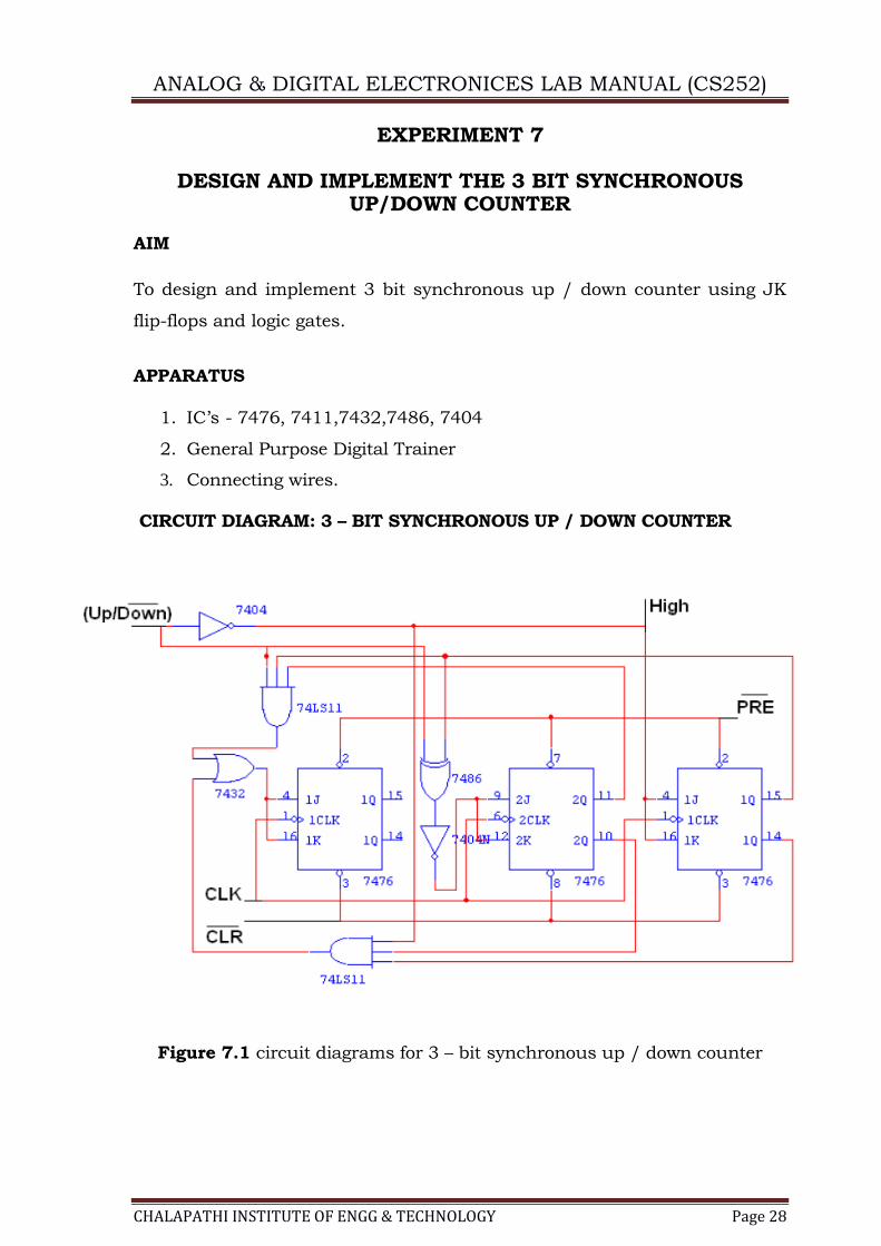
EXPERIMENT 7
DESIGN AND IMPLEMENT THE 3 BIT SYNCHRONOUS UP/DOWN COUNTER
AIM
To design and implement 3 bit synchronous up / down counter using JK
flip-flops and logic gates.
APPARATUS
1. IC’s - 7476, 7411,7432,7486, 7404
2. General Purpose Digital Trainer
3. Connecting wires.
CIRCUIT DIAGRAM: 3 – BIT SYNCHRONOUS UP / DOWN COUNTER
Figure 7.1 circuit diagrams for 3 – bit synchronous up / down counter

ANALOG & DIGITAL ELECTRONICES LAB MANUAL (CS252)
CHALAPATHI INSTITUTE OF ENGG & TECHNOLOGY Page 29
TRUTH TABLE:
Up Counter Down Counter
CLK QA QB QC QA QB QC
0 0 0 0 1 1 1
1 0 0 1 1 1 0
2 0 1 0 1 0 1
3 0 1 1 1 0 0
4 1 0 0 0 1 1
5 1 0 1 0 1 0
6 1 1 0 0 0 1
7 1 1 1 0 0 0
8 0 0 0 1 1 1
PIN DIAGRAM

ANALOG & DIGITAL ELECTRONICES LAB MANUAL (CS252)
CHALAPATHI INSTITUTE OF ENGG & TECHNOLOGY Page 30
THEORY
A counter is a register capable of counting number of clock pulse arriving at
its clock input. Counter represents the number of clock pulses arrived. In
synchronous counters, the clock inputs of all the flip-flops are connected
together and are triggered by the input pulses. Thus, all the flip-flops
change state simultaneously (in parallel). An up/down counter is one that is
capable of progressing in increasing order or decreasing order through a
certain sequence. An up/down counter is also called bidirectional counter.
Usually up/down operation of the counter is controlled by up/down signal.
When this signal is high counter goes through up sequence and when
up/down signal is low counter follows reverse sequence
PROCEDURE
Decade Counter (Mod-Counter)
1. Connect the circuit as shown in figure 9.1
2. Apply 5V supply between V CC and ground pins of all ICs.
3. Apply 5V for logic „1‟ level and 0V for logic „0‟ level.
4. Apply logic 1 to J input of any flip flop
5. Apply clock pulses from the pulse generator.
6. Observe the count sequence at Q 8 , Q 4 , Q 2 , Q 1 terminals as in
table

ANALOG & DIGITAL ELECTRONICES LAB MANUAL (CS252)
CHALAPATHI INSTITUTE OF ENGG & TECHNOLOGY Page 31
Up Counter
1. Connect the circuit as shown in figure 9.2
2. Apply 5V supply between V CC and ground pins of all ICs.
3. Apply 5V for logic „1‟ level and 0 V for logic „0‟ level.
4. Apply logic 1 at J input of any Flip-flop.
5. Apply clock pulses from pulse generator and observe the count
sequence as in table
Down Counter
1. Connect the circuit as shown in figure 9.3
2. Apply 5V supply between V CC and ground pins of all ICs.
3. Apply 5V for logic „1‟ level and 0 V for logic „0‟ level.
4. Apply logic 1 at J input of any Flip-flop.
5. Apply clock pulses from pulse generator and observe the count
sequence as in table
NOTE Initially set all the FFs using PR inputs.
Up/Down Counter
1. Connect the circuit as shown in figure 9.4
2. Apply 5V supply between V CC and ground pins of all ICs.
3. Apply 5V for logic „1‟ level and 0 V for logic „0‟ level.
4. Apply logic 1 at J input of any Flip flop.
5. Apply clock pulses from pulse generator and observe the count
sequence as in table 9.4.
6.
NOTE Initially clear all the FFs using clear inputs.
PRECAUTIONS
1. Correct ICs should be properly placed on the IC bases using pin
diagrams.
2. The open circuit voltage of the power supply should be exactly 5
Volts.

ANALOG & DIGITAL ELECTRONICES LAB MANUAL (CS252)
CHALAPATHI INSTITUTE OF ENGG & TECHNOLOGY Page 32
RESULT
The operations of 3 bit synchronous up / down counter using JK flip-flops
was designed successfully using IC 7476 and its truth table was verified.
VIVA QUESTIONS
1. What is the difference between ripple counter and synchronous
counter?
2. Which types of counters are faster, ripple or synchronous?
3. What are the applications of Asynchronous Counters?
4. What are the applications of MOD-10 Counters?

ANALOG & DIGITAL ELECTRONICES LAB MANUAL (CS252)
CHALAPATHI INSTITUTE OF ENGG & TECHNOLOGY Page 33
EXPERIMENT 8
CHARACTERISTICS OF COMMON BASE CONFIGURATION
AIM
To plot the Input and Output characteristics of a transistor connected in
Common Base Configuration and to find the h – parameters from the
characteristics.
APPARATUS
CIRCUIT DIAGRAM
MODEL GRAPHS:
1. Plot the Input characteristics by taking IE on y–axis and VEB on x–axis.
2. Plot the Output characteristics by taking IC on y–axis and VCB on x–axis.

ANALOG & DIGITAL ELECTRONICES LAB MANUAL (CS252)
CHALAPATHI INSTITUTE OF ENGG & TECHNOLOGY Page 34
PROCEDURE TO FIND THE INPUT CHARACTERISTICS:
1. Connect the circuit as in the circuit diagram.
2. Keep VEE and VCC in zero volts before giving the supply
3. Set VCB = 1 volt by varying VCC and vary the VEE smoothly with
fine control such that emitter current IE varies in steps of 0.2mA
from zero up to 20mA, and note down the corresponding voltage
VEB for each step in the tabular form.
4. Repeat the experiment for VCB =2 volts and 3 volts.
5. Draw a graph between VEB Vs IE against VCB = Constant.
TO FIND THE OUTPUT CHARACTERISTICS:
1. Start VEE and VCC from zero Volts.
2. Set the IE = 1mA by using VEE such that, VCB changes in steps of
1.0 volts from zero up to 20 volts, note down the corresponding
collector current IC for each step in the tabular form.
3. Repeat the experiment for IE = 3mA and IE = 5mA, tabulate the
readings.
4. Draw a graph between VCB Vs IC against IE = Constant.

ANALOG & DIGITAL ELECTRONICES LAB MANUAL (CS252)
CHALAPATHI INSTITUTE OF ENGG & TECHNOLOGY Page 35
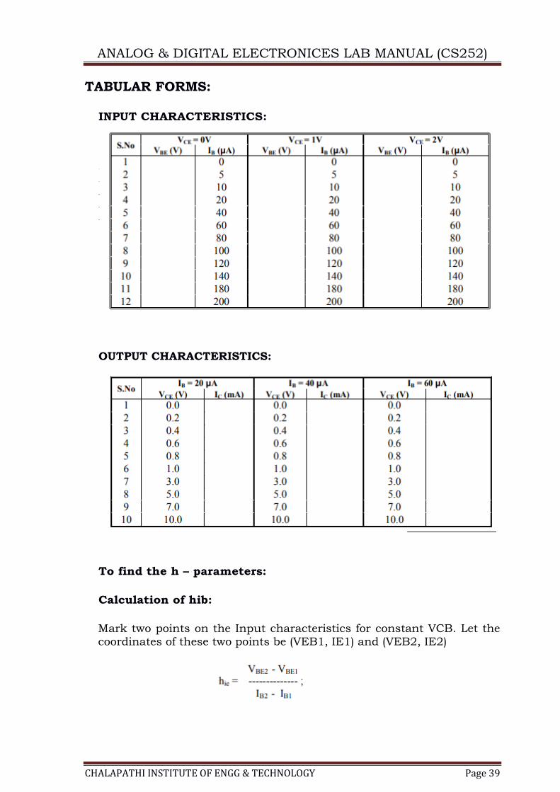
TABULAR FORMS:
INPUT CHARACTERISTICS
OUTPUT CHARACTERISTICS:
To find the h – parameters:
Calculation of hib:
Mark two points on the Input characteristics for constant VCB.
Let the coordinates of these two points be (VEB1, IE1) and (VEB2, IE2).
ANALOG & DIGITAL ELECTRONICES LAB MANUAL (CS252)
CHALAPATHI INSTITUTE OF ENGG & TECHNOLOGY Page 36
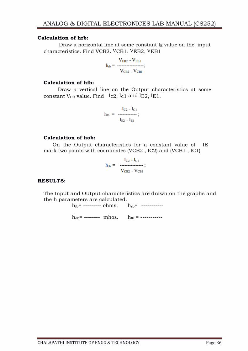
Calculation of hrb:
Draw a horizontal line at some constant IE value on the input
characteristics. Find VCB2, VCB1, VEB2, VEB1
Calculation of hfb:
Draw a vertical line on the Output characteristics at some
constant VCB value. Find Ic2, Ic1 and IE2, IE1.
Calculation of hob:
On the Output characteristics for a constant value of IE mark two points with coordinates (VCB2 , IC2) and (VCB1 , IC1)
RESULTS:
The Input and Output characteristics are drawn on the graphs and
the h parameters are calculated.
hib= --------- ohms. hrb= -----------
hob= -------- mhos. hfb = -----------

ANALOG & DIGITAL ELECTRONICES LAB MANUAL (CS252)
CHALAPATHI INSTITUTE OF ENGG & TECHNOLOGY Page 37
EXPERIMENT 9
CHARACTERISTICS OF COMMON EMITTER
CONFIGURATION
AIM
To plot the Input and Output characteristics of a transistor connected in
Common Emitter Configuration and to find the h – parameters from the
characteristics.
APPARATUS
CIRCUIT DIAGRAM
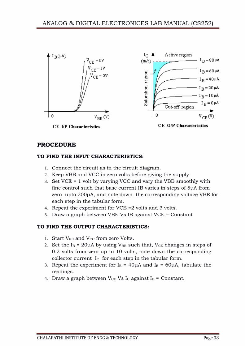
MODEL GRAPHS:
1. Plot the Input characteristics by taking IB on y-axis and VBE on x-axis.
2. Plot the Output characteristics by taking IC on the y-axis and VCE on
x-axis.
ANALOG & DIGITAL ELECTRONICES LAB MANUAL (CS252)
CHALAPATHI INSTITUTE OF ENGG & TECHNOLOGY Page 38
PROCEDURE TO FIND THE INPUT CHARACTERISTICS:
1. Connect the circuit as in the circuit diagram.
2. Keep VBB and VCC in zero volts before giving the supply
3. Set VCE = 1 volt by varying VCC and vary the VBB smoothly with
fine control such that base current IB varies in steps of 5μA from
zero upto 200μA, and note down the corresponding voltage VBE for
each step in the tabular form.
4. Repeat the experiment for VCE =2 volts and 3 volts.
5. Draw a graph between VBE Vs IB against VCE = Constant
TO FIND THE OUTPUT CHARACTERISTICS:
1. Start VEE and VCC from zero Volts.
2. Set the IB = 20μA by using VBB such that, VCE changes in steps of
0.2 volts from zero up to 10 volts, note down the corresponding
collector current IC for each step in the tabular form.
3. Repeat the experiment for IE = 40μA and IE = 60μA, tabulate the
readings.
4. Draw a graph between VCE Vs IC against IB = Constant.
ANALOG & DIGITAL ELECTRONICES LAB MANUAL (CS252)
CHALAPATHI INSTITUTE OF ENGG & TECHNOLOGY Page 39
TABULAR FORMS:
INPUT CHARACTERISTICS:
OUTPUT CHARACTERISTICS:
To find the h – parameters:
Calculation of hib:
Mark two points on the Input characteristics for constant VCB. Let the coordinates of these two points be (VEB1, IE1) and (VEB2, IE2)

ANALOG & DIGITAL ELECTRONICES LAB MANUAL (CS252)
CHALAPATHI INSTITUTE OF ENGG & TECHNOLOGY Page 40
Calculation of hrb:
Draw a horizontal line at some constant IE value on the input
characteristics. Find VCB2, VCB1, VEB2, VEB1
Calculation of hfb:
Draw a vertical line on the Output characteristics at some
constant VCB value. Find Ic2, Ic1 and IE2, IE1.
Calculation of hob:
On the Output characteristics for a constant value of IE
mark two points with coordinates (VCB2 , IC2) and (VCB1 , IC1).
RESULTS:
The input and output characteristics are drawn on the graphs and
the h parameters are calculated.
hie= --------- ohms. hre= -----------
hoe= -------- mhos. hfe = -----------