european company profiles - smithsonian...
TRANSCRIPT
INTEGRATED CIRCUIT ENGINEERING CORPORATION 3-1
European Company Profiles Alcatel Mietec
ALCATEL MIETEC
Alcatel MietecRaketstraat 62
B-1130 Brussels, BelgiumTelephone: (32) (2) 7281811
Fax: (32) (2) 7264215
IC Manufacturer
Regional Headquarters/Representative Locations
North America: Alcatel Mietec • Richardson, TexasTelephone: (214) 996-5000 • Fax: (214) 996-7062
Financial History ($M)
1992 1993 1994 1995 1996
Sales 113 148 163 170 205Capital Expenditures 65 17 24 87 37
Employees 500 540 560 635 723
Company Overview and Strategy
Mietec was formed in 1983 as a joint venture between Bell Telephone Manufacturing Company (BTMC) ofBelgium (then owned by ITT) and Gewestelijke Investerings Maatschapij voor Vlaanderen (GIMV), theFlanders regional investment company. The company's first wafer fab was at full production by 1985. In1987, ITT's telecom activities were merged into Alcatel; thus BTMC became part of the Alcatel group andAlcatel became part owner of Mietec. In 1990, Alcatel purchased all of the shares in Mietec and renamedthe operation Alcatel Mietec.
Alcatel Mietec is a leading designer, developer, and marketer of digital and mixed-signal ASICs fortelecommunications, automotive, and industrial systems. The firm is Europe's leading digital and mixed-signal standard cell ASIC producer. Approximately 65 percent of its ASICs are for the parent company'suse. The company is aiming to increase its merchant market sales from 35 percent to 50 percent, byexpanding in Europe, the U.S., and Asia. In addition, Alcatel Mietec has been aggressively marketing itsapplication-specific standard products (ASSPs).

3-2
INTEGRATED CIRCUIT ENGINEERING CORPORATION
Alcatel Mietec European Company Profiles
Management
Walter Mattheus Managing DirectorLeon Cloetens Director, Product DevelopmentPieter Doms Director, OperationsJozef D'Haene Director, Finance and AdministrationVincent Roland Director, Sales and MarketingEric Schutz Director, Quality, Research, and TechnologyJan Van Acoleyen Director, Human Resources
Products and Processes
Alcatel Mietec focuses on the design and production of cell-based ASICs and ASSPs fortelecommunications, consumer electronics, automotive, motor/motion control, and portable electronicsapplications. Its products are manufactured using primarily advanced submicron CMOS and high-voltageBiCMOS processes. Most processes feature accurate poly to poly capacitors and high ohmic poly resistorsdedicated to the design of advanced analog front-ends. The company claims to be Europe’s first topropose 0.5µm analog processing for manufacturing ASICs.
In 1996, Alcatel Mietec decided to focus its ASSP development on telecommunications products and morespecifically on digital modems like XDSL. The company, who has been an early promoter of ISDN,revamped its ISDN offerings by using embedded processors (e.g., 16-/32-bit ARM7) and advanced 0.5µmCMOS analog technology to significantly reduce the cost of ISDN solutions. In addition, the companylaunched its first ADSL chipset.
Also in 1996, Alcatel Mietec started production of an advanced smart power process called I2T offering highvoltage DMOS transistors featuring 0.7µm CMOS technology.
Semiconductor Fabrication Facilities
Alcatel Mietec Alcatel MietecWesterring 15 Westerring 15B-9700 Oudenaarde B-9700 OudenaardeBelgium BelgiumFab 1 Fab 2Cleanroom size: 21,530 square feet (Class 10) Cleanroom size: 37,500 square feet (Class 1)Capacity (wafers/week): 2,500 Capacity (wafers/week): 2,500Wafer size: 100mm Wafer size: 150mmProcesses: NMOS, CMOS, BiCMOS, BCDMOS Process: CMOSProducts: Cell-based ASICs, ASSPs, custom ICs Products: Cell-based ASICs, ASSPs, custom ICsFeature sizes: 1.2µm, 1.5µm, 2.0µm, 3.0µm Feature sizes: 0.35µm, 0.5µm, 0.7µm, 1.2µm

INTEGRATED CIRCUIT ENGINEERING CORPORATION 3-3
European Company Profiles Alcatel Mietec
Key Agreements
• Alcatel Mietec established a license agreement with Advanced RISC Machines in the U.K. for the ARM7Thumb RISC microprocessor core.
• Alcatel Mietec is working with IMEC, Belgium's microelectronics R&D center, to develop 0.35µm and finergeometry process technologies.
• Alcatel Mietec has had a technological partnership agreement with SGS-Thomson since 1987.

3-4
INTEGRATED CIRCUIT ENGINEERING CORPORATION
Austria Mikro Systeme European Company Profiles
AUSTRIA MIKRO SYSTEME (AMS)
Austria Mikro Systeme International AGSchloss Premstätten
A-8141 UnterpremstättenAustria
Telephone: (43) 3136-500-0Fax: (43) 3136-52501/53650Web Site: www.ams.co.at
IC Manufacturer
Regional Headquarters/Representative Locations
North America: AMS, Inc. • Cupertino, CaliforniaTelephone: (408) 865-1217 • Fax: (408) 865-1219
Financial History ($M), Fiscal Year Ends December 31
1992 1993 1994 1995 1996
Sales 59 68 95 175 173Net Income 4 5 13 22 10R&D Expenditures 9 12 13 25 21Capital Expenditures 11 12 26 36 10
Employees 584 600 648 1,512 1,105
Company Overview and Strategy
Austria Mikro Systeme International, or AMS, was founded in 1981 as a joint venture between Voest-AlpineAG, the Austrian state-owned industrial group, and American Microsystems, Inc. of California. In 1987, AMSbecame jointly owned by Voest-Alpine and Austrian Industries Technologies, another state-owned company.The Austrian government remained in control until June 1993, when AMS became a public company.
Initially, AMS focused on the manufacture of standard products, but financial troubles soon took hold of thecompany. In 1986, the company was streamlined and restructured to focus on its skills in mixed-signaltechnology. Today, the company specializes in the development and production of mixed-signal ASICs. Itprovides a range of custom and semicustom MOS/VLSI capabilities, including full custom circuits and high-performance analog and digital cells based on CMOS and BiCMOS process technologies. AMS’s productstarget the communications, automotive, and industrial electronics market segments.
INTEGRATED CIRCUIT ENGINEERING CORPORATION 3-5
European Company Profiles Austria Mikro Systeme
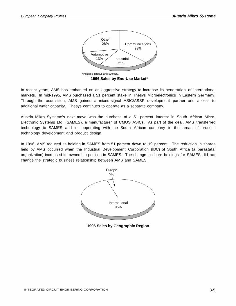
Communications38%
1996 Sales by End-Use Market*
Automotive13% Industrial
21%
Other28%
*Includes Thesys and SAMES.
In recent years, AMS has embarked on an aggressive strategy to increase its penetration of internationalmarkets. In mid-1995, AMS purchased a 51 percent stake in Thesys Microelectronics in Eastern Germany.Through the acquisition, AMS gained a mixed-signal ASIC/ASSP development partner and access toadditional wafer capacity. Thesys continues to operate as a separate company.
Austria Mikro Systeme’s next move was the purchase of a 51 percent interest in South African Micro-Electronic Systems Ltd. (SAMES), a manufacturer of CMOS ASICs. As part of the deal, AMS transferredtechnology to SAMES and is cooperating with the South African company in the areas of processtechnology development and product design.
In 1996, AMS reduced its holding in SAMES from 51 percent down to 19 percent. The reduction in sharesheld by AMS occurred when the Industrial Development Corporation (IDC) of South Africa (a parastatalorganization) increased its ownership position in SAMES. The change in share holdings for SAMES did notchange the strategic business relationship between AMS and SAMES.
Europe5%
1996 Sales by Geographic Region
International95%

3-6
INTEGRATED CIRCUIT ENGINEERING CORPORATION
Austria Mikro Systeme European Company Profiles
Management
Horst Gebert President and Chief Executive OfficerHartwin Breitenbach Director, MarketingVolker Kempe, Ph.D. Director, EngineeringHeribert Lecker Director, LogisticsWalter Mente Director, Product AssuranceKarl Müller, Ph.D. Director, FacilityHumbert Noll, Ph.D. Director, Research and DevelopmentHeimo Pirket, Ph.D. Director, Human ResourcesGerhard Richter Director, ManufacturingJohann Stritzelberger Director, Finance and Chief Financial Officer
Products and Processes
AMS specializes in the production and development of ASICs and provides a full range of custom circuits forcommunications, automotive, and industrial electronics applications. In addition, AMS provides silicon waferfoundry services for customer-designed ICs. The company’s products and services are outlined below.
• Communication circuits include single-chip telephones, dialers, line adapters, modems, codecs, filters,ringers, and speech amplifiers.
• Automotive circuits include devices for ignition and motor controls, safety systems, airbags, and lighting.• Industrial electronics circuits include ICs for analog and digital controls for civilian aviation, advanced
instrumentation, enhanced robotics, and environmental protection.• Display drivers• Foundry services
The company’s digital standard cells are available in extensive libraries in 0.6µm, 0.8µm, 1.0µm, 1.2µm, and2.0µm double-metal CMOS and BiCMOS technologies. Over 70 percent of AMS designed custom circuitsinclude analog circuitry. AMS provides a variety of analog functions in cell form using 1.2µm and 2.0µmdouble-metal, double-poly processes.
Semiconductor Fabrication Facilities
Austria Mikro Systeme International AGSchloss PremstättenA-8141 Unterpremstätten, AustriaCleanroom size: 35,000 square feet (Class 1-10)Capacity (wafers/week): 3,500Wafer size: 100mmProcesses: CMOS, BiCMOSProducts: ASICs, design and foundry servicesFeature sizes: 0.8µm-2.0µm BiCMOS; 0.6µm-1.2µm CMOS

INTEGRATED CIRCUIT ENGINEERING CORPORATION 3-7
European Company Profiles Austria Mikro Systeme
AMS uses Taiwan Semiconductor Manufacturing Company (TSMC) and United Microelectronics Corporation(UMC) as foundries to supplement its internal capacity for its older products.
The company has design centers in Paris, Milan, London, Munich, Hamburg, Dresden, Stockholm, andBudapest, as well as in Cupertino, California.
Key Agreements
• AMS has an international license and wafer foundry agreement with SAMES. Under the agreementSAMES produces and markets AMS single-chip telephone ICs in South Africa. During 1996, AMSreduced its interest in SAMES to 19 percent. Prior to the reduction, AMS had a 51 percent controllinginterest.
• AMS and Thesys have a product development agreement. The agreement covers free process, design,and product technology transfers from AMS to Thesys, while BiCMOS and CMOS expertise at bothcompanies is shared. AMS has a 51 percent controlling interest in Thesys.
• AMS agreed to provide Pericom Semiconductor with access to foundry services in exchange for rights tocertain BiCMOS technologies from Pericom. AMS is producing Pericom's FCT logic devices using 0.8µmCMOS and BiCMOS processes.
• AMS fabricates wafers for India’s Semiconductor Complex Limited, whose fab was destroyed in a fire.
• AMS and Mitel Semiconductor have a product development and foundry relationship.
• AMS and Asahi Kasei Microsystems (AKM) have a multi-year cross-licensing agreement covering severalproducts in the telecom field.
• AMS joined the Esprit project to develop 8-bit, 16-bit, and 20-bit converters for telecommunications anddata transmission applications.
• AMS is participating in a Eureka Fab 2000 project to develop an ASIC concept which allows theintegration of high performance analog functions with complex logic elements.

3-8
INTEGRATED CIRCUIT ENGINEERING CORPORATION
CSEM European Company Profiles
CENTRE SUISSE D’ELECTRONIQUEET DE MICROTECHNIQUE SA (CSEM)
Centre Suisse d'Electronique et deMicrotechnique SA
Jaquet-Draz 1CH-2007 Neuchâtel, Switzerland
Telephone: (41) (38) 205-111Fax: (41) (38) 205-700
Web Site: www.csem.ch
IC Manufacturer
Financial History ($M)
1992 1993 1994 1995 1996
Corporate Sales 51 56 62 66 71IC Design Sales 13 15 16 20 20
Employees 336 336 348 384 411
Company Overview and Strategy
CSEM is a privately held research, development, and specialized production company based in Switzerland.Of CSEM’s total staff, approximately 20 percent are engaged in the production of full custom low-powermixed-mode ICs. CSEM’s activities cover microelectronics, microsystems, subsystems, and instrumentation,as well as bio-inspired systems. The company was founded in 1984, but its origins date back to 1924 withits involvement in the watch industry. The first monolithic watch IC was developed by CSEM engineers in1967.
CSEM focuses its IC design expertise on the research, specification, development, and production ofcustom integrated circuits and systems for miniature, portable, and body-worn products, where low-power,low-voltage, high system complexity, functionality and a minimum of external components are essential.Design expertise includes low power, low voltage (down to 0.9V), RF (up to 2.5 GHz), analog/digital,EEPROM on-chip and remote sensing, as well as the CoolRISC family of low-power RISC-architecturemicroprocessor cores.
Management
Thomas Hinderling, Ph.D. Chief Executive OfficerEvert Dijkstra Head and Commercial Director, CSEM IC DesignJean-Paul Bardyn, Ph.D. Deputy Head and Technical Director, CSEM IC Design

INTEGRATED CIRCUIT ENGINEERING CORPORATION 3-9
European Company Profiles CSEM
Products and Processes
CSEM IC Design is engaged in the production of full custom mixed-mode ICs. Other activities includesilicon-based sensor and actuator systems, low-power microprocessors, thin films and coatings, metrologyand instruments, optics, radio communication, industrial control systems, data communications, as well astelemetry and remote sensing.
Semiconductor Fabrication Facilities
CSEM IC Design is a fabless design center. CSEM’s own fab is used for producing prototypes. Volume ICproduction is subcontracted out to its manufacturing partners who include TSMC in Taiwan, and EMMicroelectronic-Marin, Faselec, SGS-Thomson Microelectronics, and Alcatel Mietec in Europe.
• TSMC for 1.0µm, 0.5µm, and 0.35µm, mixed-signal CMOS process technologies.• Faselec for 2.0µm, mixed-signal, EEPROM, OTP CMOS and 1.0µm mixed-signal CMOS process
technologies.• EM Microelectronic-Marin for 2.0µm and 1.0µm, mixed-signal and EEPROM CMOS process technologies.• SGS-Thomson Microelectronics for 1.2µm, 0.7µm, and 0.5µm BiCMOS and 0.7µm CMOS, EEPROM
process technologies.• Alcatel Mietec for 0.7µm and 0.5µm, mixed-signal CMOS and 0.7µm high voltage CMOS process
technologies.
3-10
INTEGRATED CIRCUIT ENGINEERING CORPORATION
Dialog Semiconductor European Company Profiles
DIALOG SEMICONDUCTOR
Dialog Semiconductor Limited(Member of TEMIC Semiconductors)
Windmill Hill, Whitehill WaySwindon SN5 6PJUnited Kingdom
Telephone: (44) (1793) 875327Fax: (44) (1793) 875328
Fabless IC Supplier
Regional Headquarters/Representative Locations
North America: Dialog Semiconductor North America c/o TEMIC • Basking Ridge, New JerseyTelephone: (908) 630-9095 • Fax: (908) 630-9096
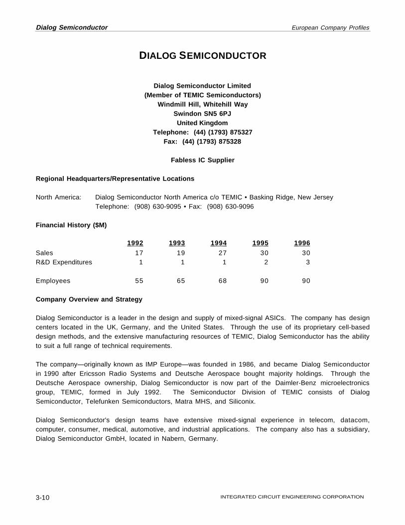
Financial History ($M)
1992 1993 1994 1995 1996
Sales 17 19 27 30 30R&D Expenditures 1 1 1 2 3
Employees 55 65 68 90 90
Company Overview and Strategy
Dialog Semiconductor is a leader in the design and supply of mixed-signal ASICs. The company has designcenters located in the UK, Germany, and the United States. Through the use of its proprietary cell-baseddesign methods, and the extensive manufacturing resources of TEMIC, Dialog Semiconductor has the abilityto suit a full range of technical requirements.
The company—originally known as IMP Europe—was founded in 1986, and became Dialog Semiconductorin 1990 after Ericsson Radio Systems and Deutsche Aerospace bought majority holdings. Through theDeutsche Aerospace ownership, Dialog Semiconductor is now part of the Daimler-Benz microelectronicsgroup, TEMIC, formed in July 1992. The Semiconductor Division of TEMIC consists of DialogSemiconductor, Telefunken Semiconductors, Matra MHS, and Siliconix.
Dialog Semiconductor's design teams have extensive mixed-signal experience in telecom, datacom,computer, consumer, medical, automotive, and industrial applications. The company also has a subsidiary,Dialog Semiconductor GmbH, located in Nabern, Germany.

INTEGRATED CIRCUIT ENGINEERING CORPORATION 3-11
European Company Profiles Dialog Semiconductor
Communication75%
1996 Sales by End-Use Market
Automotive10%
Industrial12%
Other3%
Management
Roland Pudelko Managing DirectorGary Duncan Vice President, MarketingPeter Hall Vice President, Manufacturing OperationsRichard Schmitz Vice President, Engineering
Products and Processes
Dialog Semiconductor supplies mixed-signal ASICs using a range of (0.7µm to 3.0µm) double-poly, double-metal CMOS processes to suit differing application needs. For special needs, BiCMOS, bipolar, andEEPROM processes are sourced according to requirement.
Dialog Semiconductor has used this technology to develop a large number of mixed-signal ASICs for use ina wide range of markets and applications as outlined below.
Communications Industrial
• Audio processing • Switch mode PSU• Line transceivers • Flow meter• Modems • LCD decoder/driver• Frequency synthesis • Blood sugar measurement• Baseband interface • Bar code reader• Echo cancellation • Heartrate analyzer• Control and monitoring • Remote metering• Power supply management
Automotive Computer and Consumer
• Intruder alarms • HDD spindle motor control• Acceleration sensors • Video DAC/ADC• Pressure sensors • Audio DAC/ADC• Signal conditioning • Music synthesizer• Active suspension control • HDD head park• Throttle valve sensors
3-12
INTEGRATED CIRCUIT ENGINEERING CORPORATION
Elmos European Company Profiles
ELMOS
Elmos GmbHJoseph-von-Fraunhofer-Strasse 9
44227 Dortmund, GermanyTelephone: (49) (231) 7549-0
Fax: (49) (231) 7549-159
IC Manufacturer
Employees 300
Company Overview and Strategy
Established in 1984, Elektronik in MOS-Technologie GmbH (Elmos) specializes in the design and productionof analog, digital, and mixed-signal ASICs. The company is privately owned with BMW-subsidiary Intech ofMunich, Germany, being the largest shareholder (30 percent). The majority of Elmos’ devices are sold toautomotive-subsystem makers primarily in Europe, but also in North America and Japan. The remaindergoes to consumer equipment companies and into industrial applications.
Management
Klaus Weyer PresidentEberhard Knapp President and Chief Operating OfficerKnut Hinrichs President and Chief Financial Officer
Products and Processes
Elmos uses proprietary N-well silicon-gate CMOS process technology in the design and fabrication of itsASIC products, which include analog, mixed-signal, and most recently digital devices. In late 1995, thecompany introduced its designs of 8-bit RISC microcontroller cores to provide intelligence to its mixed-signalautomotive ASICs.
Semiconductor Fabrication Facilities
Elmos GmbHDortmund, GermanyCapacity (wafers/week): 1,500Wafer sizes: 100mm, 150mmProcess: CMOSProducts: ASICsFeature sizes: ≥1.0µm
Elmos also uses Siemens as a foundry for the production of high-voltage automotive-related CMOS ASICs.
INTEGRATED CIRCUIT ENGINEERING CORPORATION 3-13
European Company Profiles EM Microelectronic-Marin
EM MICROELECTRONIC-MARIN
EM Microelectronic-Marin SARue des Sors 3
CH-2074 Marin, SwitzerlandTelephone: (41) (32) 755-5111
Fax: (41) (32) 755-5403Web Site: www.emmarin.ch
IC Manufacturer
Regional Headquarters/Representative Locations
North America: EM Microelectronic USA • Richardson, TexasTelephone: (214) 238-8184 • Fax: (214) 238-7661
Financial History ($M)
1992 1993 1994 1995 1996
Sales 45 55 65 84 95
Employees 283 285 285 290 330
Company Overview and Strategy
EM Microelectronic-Marin was founded in 1975 as a division of the Swiss Ebauches Electronics SA, whichwas a member of the ASUAG group of companies. Nearly ten years later this group merged with the SSIHgroup to form the new SMH, the largest Swiss group of companies manufacturing watches andmicroelectronics. At the same time, the Microelectronic-Marin division was formed into an independentcompany, EM Microelectronic-Marin SA.
Today, the company is a leading manufacturer of low-power, low-voltage CMOS products. Although itbegan life as a chip supplier to watch manufacturers, today about 50 percent of its devices are industrialcircuits. The company is striving to become a major supplier in the field of user-specific, customized andstandard low-power, low-voltage CMOS circuits for the electronics industry. EM Microelectronic-Marin alsofunctions as a foundry for various processes. Furthermore, the firm offers a bumping service for 100mm and150mm wafer sizes.
EM Microelectronic-Marin set up a U.S. sales network and is now offering standard and semicustomproducts to the American market. Through the move, the company hopes to parlay its productioncapabilities into higher sales beyond Europe.
3-14
INTEGRATED CIRCUIT ENGINEERING CORPORATION
EM Microelectronic-Marin European Company Profiles
Management
Mougahed Darwish PresidentPaul Aebersold Director, Finance and AdministrationDieter Diegel Director, Sales and MarketingGunther Meusburger Director, DesignManfred Meyer Director, Back-End ProductionMartin Schwander Director, Front-End ProductionPierre Tschirren Director, Quality
Products and Processes
EM Microelectronic-Marin manufactures and sells watch and clock circuits, LCD drivers, 4-bit microcontrollersfor embedded applications (1.2V to 5V), and mixed-signal ASICs and full custom ICs. The company alsoprovides contactless identification devices (CID) for the electronic identification industry.
The company started out using CMOS technology for making watch circuits. It developed this technologyfurther to use even lower power consumption and to operate at low battery voltages, down to less than 1V. As a result of its 16 years of experience in the watch IC industry, it has become a specialist in low-power, low-voltage CMOS circuits. Its current process technology portfolio includes the following: 3.0µm P-well CMOS;single-metal, 2.0µm N-well CMOS; and double-metal 1.5µm and 1.0µm CMOS. These processes allow forthe combination of analog and digital functions, as well as EEPROM on a single chip. In 1996, thecompany began development on a 0.5µm process technology.
Semiconductor Fabrication Facilities
EM Microelectronic-Marin SARue des Sors 3CH-2074 Marin, SwitzerlandCleanroom size: 35,000 square feetCapacity (wafers/week): 1,600Wafer size: 150mmProcess: CMOSProducts: Timepiece, power controller, and telecom ICs;
LCD drivers; real-time clocks; ASICs; EEPROMs; MCUsFeature sizes: 1.0µm, 1.5µm, 2.0µm, 3.0µm (0.5µm in development)

INTEGRATED CIRCUIT ENGINEERING CORPORATION 3-15
European Company Profiles Ericsson Components
ERICSSON COMPONENTS
Ericsson Components ABMicroelectronic Access Devices
Isafjordsgatan 16S-164 81 Kista, Stockholm, Sweden
Telephone: (46) (8) 757-50-00Fax: (46) (8) 757-47-76
Web Site: www.ericsson.com
IC Manufacturer
Regional Headquarters/Representative Locations
North America: Ericsson Components • Richardson, TexasTelephone: (214) 669-9900 • Fax: (214) 680-1059
Financial History, Fiscal Year Ends December 31
1992 1993 1994 1995 1996
Corporate (SEK millions)Sales SEK47,020 SEK62,654 SEK82,554 SEK98,780 SEK124,266 Components* SEK4,479 SEK5,599 SEK6,317 SEK7,721 SEK7,793Net Income SEK478 SEK2,835 SEK3,949 SEK5,439 SEK7,110
*Internal and External Sales
Semiconductor ($M)Sales $160 $190 $240 $300 $390
Employees 1,200
Company Overview and Strategy
Ericsson Components is a subsidiary of L.M. Ericsson, a $13 billion international leader in tele-communications products. L.M. Ericsson's business units are Radio Communications, PublicTelecommunications, Business Networks, Components, and Microwave Systems. Ericsson Components'products include integrated circuits, thick-film hybrids, power transistors, optoelectronic devices, energysystems for power and cooling applications, and fiber optic cable.
Integrated circuits have been an important part of Ericsson's operations since its first production unit wasopened in the early 1970's. The company designs and manufactures microelectronic devices for analogand digital access, fiber optic access, and radio access applications in telecommunications systems.Approximately half of its semiconductor production is built into Ericsson products and systems, the remainingis sold to other telecommunications system manufacturers.

3-16
INTEGRATED CIRCUIT ENGINEERING CORPORATION
Ericsson Components European Company Profiles
Components*3%
PublicTelecommuni-
cations19%
1996 Corporate Sales byBusiness Group
MicrowaveSystems
3%BusinessNetworks
12%
RadioCommunications
63%
*External Only
North America 13%
1996 Component Sales byGeographic Region
Europe73%
ROW14%
Management
Lars Ramquist President and Chief Executive Officer, L.M. EricssonBert Jeppson Senior Vice President and President, Ericsson Components ABBo Hedfors President, Ericsson Components (U.S.)
Products and Processes
Ericsson’s microelectronics activities are focused on the development and production of specializedcomponents for telecommunications systems. Its products consist of line interface modules, line access ICs,fiber optic receiver and transmitter modules, radio ICs, RF power transistors, and line protection circuits.
Ericsson uses a variety of process technologies, including high-voltage silicon bipolar technologies for lineinterface circuits, high-frequency bipolar technologies for radio ICs, 1.2µm CMOS for digital transmissionnetwork access circuits, and InP for fiber optic devices. The company’s newest fab in Kista, Sweden, is usedprimarily for R&D and rapid prototyping of ICs using 0.5µm CMOS and BiCMOS technologies, and is capableof upgrading to future 0.35µm technology.
Semiconductor Fabrication Facilities
Ericsson Components Ericsson ComponentsKista, Sweden Kista, SwedenCapacity (wafers/week): 6,250 Cleanroom size: 17,800 square feet (Class 1)Wafer size: 100mm Capacity (wafers/week): 250Processes: Bipolar, CMOS Wafer size: 150mmProducts: Telecom ICs, RF circuits, discretes, Processes: CMOS, BiCMOS optoelectronics Products: R&D, ASICsFeature sizes: 1.2µm, 1.5µm Feature size: 0.5µm (0.35µm capable)

INTEGRATED CIRCUIT ENGINEERING CORPORATION 3-17
European Company Profiles Ericsson Components
Key Agreements
• Ericsson has maintained a strategic partnership with Texas Instruments since 1987. The partnersextended their alliance in 1992 when they announced plans to construct Ericsson's pilot production fab inKista, Sweden. Under the agreement, TI installed its 0.5µm process technology in the plant in exchangefor a greater share of Ericsson's semiconductor business. TI’s 0.35µm technology will be installed in thefuture. The agreement also includes the cross-licensing of certain technologies and joint development ofadvanced ICs for telecommunications applications.

3-18
INTEGRATED CIRCUIT ENGINEERING CORPORATION
GEC Plessey Semiconductors European Company Profiles
GEC PLESSEY SEMICONDUCTORS (GPS)
GEC Plessey Semiconductors Ltd.Cheney Manor, Swindon
Wilshire SN2 2QWUnited Kingdom
Telephone: (44) (1793) 518000Fax: (44) (1793) 518411
Web Site: www.gpsemi.com
IC Manufacturer
Regional Headquarters/Representative Locations
North America: GEC Plessey Semiconductors Inc. • Scotts Valley, CaliforniaTelephone: (408) 438-2900 • Fax: (408) 438-7023
Japan: GEC Plessey Semiconductors • Chiyoda-ku, Tokyo, JapanTelephone: (81) (3) 5276-5501 • Fax: (81) (3) 5276-5510
Asia-Pacific: GEC Plessey Semiconductors • Taipei, TaiwanTelephone: (886) (2) 5461260 • Fax: (886) (2) 7190260
Financial History ($M)
1992 1993 1994 1995 1996
Sales 383 311 337 377 340IC Sales 352 290 312 342 305Discrete Sales 31 21 25 35 35
R&D Expenditures 50 60 60Capital Expenditures 44 44 64 155 60
Employees 3,500 3,300 3,300 3,000 2,700
Company Overview and Strategy
GEC Plessey Semiconductors (GPS) was originally established as Plessey Semiconductors in 1966. Thecompany became a wholly owned subsidiary of The General Electric Company plc. of England and mergedwith Marconi in 1990.

INTEGRATED CIRCUIT ENGINEERING CORPORATION 3-19
European Company Profiles GEC Plessey Semiconductors
GPS designs, produces, and markets ASICs and ASSPs aimed at three high growth market segments—communications, computing, and consumer electronics. Applications within these markets include personalradio communications (including wireless LANs and global positioning), computer peripherals, networks, andtelevisions. Its technological strengths lie in a high market penetration of RF front ends, tuning, andfrequency synthesis for both radio and TV. This is backed by expertise in high speed, high complexity digitalsignal processing and RISC processing, and broad-based experience and capability in semicustom products.The company is a leading supplier of the ARM RISC processor and of CMOS ASIC devices.
The company can be viewed as two operating divisions: Integrated Circuits and Power Semiconductors. Aswell as marketing conventional high power discretes, the Power division has launched a new range of highpower IGBTs.
Product development within GEC Plessey’s core market areas are focused on mobile telecommunications,multimedia, and networks.
CMOS Logic ICs35%
BipolarLogic ICs
3%
1996 Sales by Product Segment
Mixed-Signal ICs20%
Analog ICs29%
MPUs3%
PowerDiscretes
10%
Europe47%
ROW25%
1996 Sales by Geographic Region
North America28%
Management
GEC Plessey Semiconductors Ltd.Tom Urwin Managing DirectorJohn Brothers Director, TechnologyAlan Capper Director, Mass Storage Business UnitJohn Clifford Director, PersonnelIan Cooper Director, LegalBarry Dennington Director, ASIC System Business UnitSam Feinburg Director, Total Quality ManagementTony Gallagher Director, FinanceRay Gleason Director, Media Business UnitPhil Pollok Director, Communications/WLAN Business UnitErnie Pusey Director, Sales and MarketingJohn Reed Director, Automotive, Industrial/Military, and Power Business Unit
GEC Plessey Semiconductors Inc. (U.S.)Tom Knueppel President and General Manager
3-20
INTEGRATED CIRCUIT ENGINEERING CORPORATION
GEC Plessey Semiconductors European Company Profiles
Products and Processes
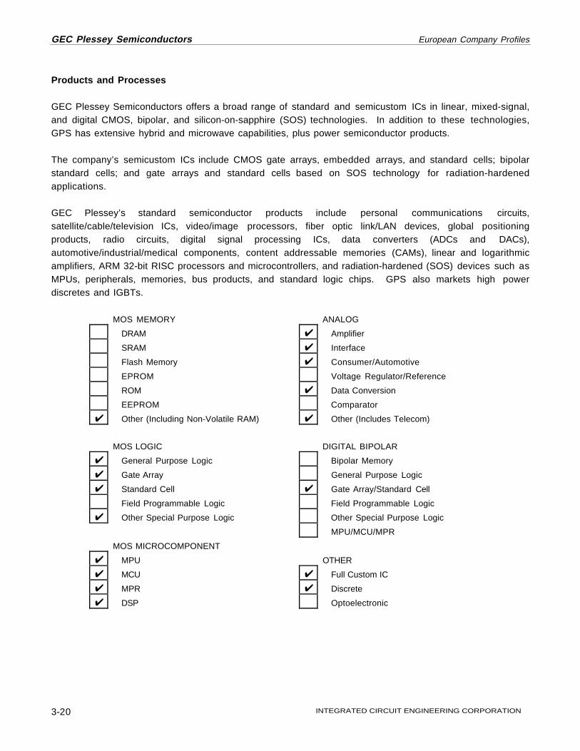
GEC Plessey Semiconductors offers a broad range of standard and semicustom ICs in linear, mixed-signal,and digital CMOS, bipolar, and silicon-on-sapphire (SOS) technologies. In addition to these technologies,GPS has extensive hybrid and microwave capabilities, plus power semiconductor products.
The company’s semicustom ICs include CMOS gate arrays, embedded arrays, and standard cells; bipolarstandard cells; and gate arrays and standard cells based on SOS technology for radiation-hardenedapplications.
GEC Plessey’s standard semiconductor products include personal communications circuits,satellite/cable/television ICs, video/image processors, fiber optic link/LAN devices, global positioningproducts, radio circuits, digital signal processing ICs, data converters (ADCs and DACs),automotive/industrial/medical components, content addressable memories (CAMs), linear and logarithmicamplifiers, ARM 32-bit RISC processors and microcontrollers, and radiation-hardened (SOS) devices such asMPUs, peripherals, memories, bus products, and standard logic chips. GPS also markets high powerdiscretes and IGBTs.
MOS MEMORY ANALOG
DRAM ✔ Amplifier
SRAM ✔ Interface
Flash Memory ✔ Consumer/Automotive
EPROM Voltage Regulator/Reference
ROM ✔ Data Conversion
EEPROM Comparator
✔ Other (Including Non-Volatile RAM) ✔ Other (Includes Telecom)
MOS LOGIC DIGITAL BIPOLAR
✔ General Purpose Logic Bipolar Memory
✔ Gate Array General Purpose Logic
✔ Standard Cell ✔ Gate Array/Standard Cell
Field Programmable Logic Field Programmable Logic
✔ Other Special Purpose Logic Other Special Purpose Logic
MPU/MCU/MPR
MOS MICROCOMPONENT
✔ MPU OTHER
✔ MCU ✔ Full Custom IC
✔ MPR ✔ Discrete
✔ DSP Optoelectronic
INTEGRATED CIRCUIT ENGINEERING CORPORATION 3-21
European Company Profiles GEC Plessey Semiconductors
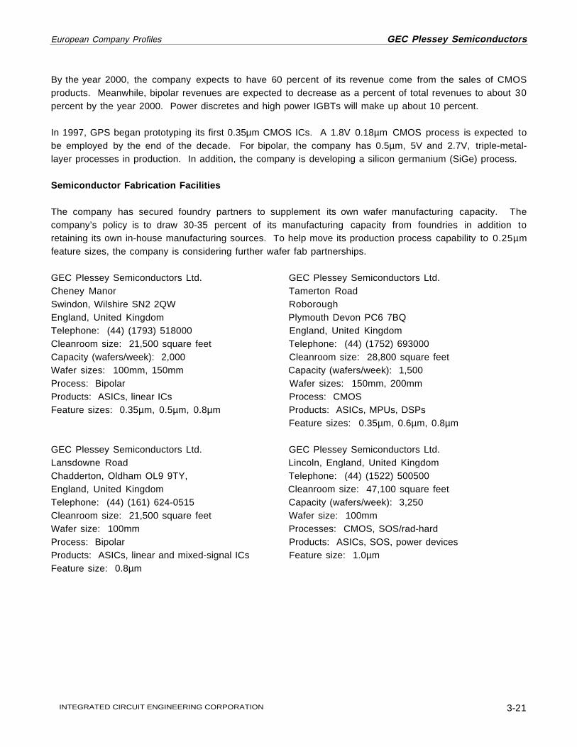
By the year 2000, the company expects to have 60 percent of its revenue come from the sales of CMOSproducts. Meanwhile, bipolar revenues are expected to decrease as a percent of total revenues to about 30percent by the year 2000. Power discretes and high power IGBTs will make up about 10 percent.
In 1997, GPS began prototyping its first 0.35µm CMOS ICs. A 1.8V 0.18µm CMOS process is expected tobe employed by the end of the decade. For bipolar, the company has 0.5µm, 5V and 2.7V, triple-metal-layer processes in production. In addition, the company is developing a silicon germanium (SiGe) process.
Semiconductor Fabrication Facilities
The company has secured foundry partners to supplement its own wafer manufacturing capacity. Thecompany’s policy is to draw 30-35 percent of its manufacturing capacity from foundries in addition toretaining its own in-house manufacturing sources. To help move its production process capability to 0.25µmfeature sizes, the company is considering further wafer fab partnerships.
GEC Plessey Semiconductors Ltd. GEC Plessey Semiconductors Ltd.Cheney Manor Tamerton RoadSwindon, Wilshire SN2 2QW RoboroughEngland, United Kingdom Plymouth Devon PC6 7BQTelephone: (44) (1793) 518000 England, United KingdomCleanroom size: 21,500 square feet Telephone: (44) (1752) 693000Capacity (wafers/week): 2,000 Cleanroom size: 28,800 square feetWafer sizes: 100mm, 150mm Capacity (wafers/week): 1,500Process: Bipolar Wafer sizes: 150mm, 200mmProducts: ASICs, linear ICs Process: CMOSFeature sizes: 0.35µm, 0.5µm, 0.8µm Products: ASICs, MPUs, DSPs
Feature sizes: 0.35µm, 0.6µm, 0.8µm
GEC Plessey Semiconductors Ltd. GEC Plessey Semiconductors Ltd.Lansdowne Road Lincoln, England, United KingdomChadderton, Oldham OL9 9TY, Telephone: (44) (1522) 500500England, United Kingdom Cleanroom size: 47,100 square feetTelephone: (44) (161) 624-0515 Capacity (wafers/week): 3,250Cleanroom size: 21,500 square feet Wafer size: 100mmWafer size: 100mm Processes: CMOS, SOS/rad-hardProcess: Bipolar Products: ASICs, SOS, power devicesProducts: ASICs, linear and mixed-signal ICs Feature size: 1.0µmFeature size: 0.8µm
3-22
INTEGRATED CIRCUIT ENGINEERING CORPORATION
GEC Plessey Semiconductors European Company Profiles
Key Agreements
• GEC Plessey is involved with the European cooperatives Esprit, Alvey, RACE, and JESSI.
• GPS is a licensed design product partner and manufacturer of the ARM RISC microprocessor.
• GPS licensed the PineDSPCore and related development tools from DSP Group Inc. in 1994. GPS isusing the 16-bit, fixed-point DSP core in ASICs and ASSPs for multimedia PC and cellular phoneapplications.

INTEGRATED CIRCUIT ENGINEERING CORPORATION 3-23
European Company Profiles ITT Semiconductors
ITT SEMICONDUCTORS
ITT SemiconductorsHans-Bunte-Strasse 19
P.O. Box 840D-79008 Freiburg
GermanyTelephone: (49) (761) 517-0
Fax: (49) (761) 517-2174Web Site: www.itt-sc.de
IC Manufacturer
Financial History ($M)
1992 1993 1994 1995 1996
Sales 181 174 198 274 255 IC Sales 118 114 121 155 180 Discrete Sales 63 60 77 119 75Capital Expenditures 26 18 39 50 40
Employees 1,759 1,710 1,745 1,918 1,831
Company Overview and Strategy
ITT Semiconductors is a fully owned subsidiary of ITT Industries, headquartered in New York (U.S.). ITTSemiconductors is part of ITT Industries’ Defense & Electronics business segment. ITT Semiconductorsoperates by the legal entity Intermetall Halbleiterwerk der Deutsche ITT Industries GmbH, located in Freiburg,Germany.
Intermetall was formed in 1952 to produce germanium transistors and diodes. Today, Intermetall designs,produces, and markets real-time signal processors, microcontrollers, and mixed-signal ICs mainly forapplication in consumer, automotive, and multimedia systems. The company also manufactures a line ofHall-effect sensor ICs and a range of discrete semiconductors. ITT Intermetall is a leader in television ICsand car instrumentation. ITT has pioneered the use of digital signal processing in entertainment systems.
Management
Tom Fischer, Ph.D. Managing DirectorWolfgang Kalsbach, Ph.D. Director, OperationsHans Nowak Director, Finance
3-24
INTEGRATED CIRCUIT ENGINEERING CORPORATION
ITT Semiconductors European Company Profiles
Products and Processes
ITT Semiconductors' IC products include DSPs, MPUs, MCUs, signal converters, video encoder/decoders,audio encoder/decoders, and Hall-effect sensors. These products are manufactured in a range of CMOStechnologies with feature sizes of 1.0µm to 0.6µm. The technologies include advanced mixed signalcapability and flash memories. Discrete products include zener diodes, Schottky diodes, varactor diodes,and small signal transistors.
Semiconductor Fabrication Facilities
ITT SemiconductorsHans-Bunte-Strasse 19P.O. Box 840D-79008 Freiburg, GermanyCleanroom size: 46,000 square feetCapacity (wafers/week): 9,500Wafer sizes: 100mm, 125mmProcesses: CMOS, planar/non-planar discretesProducts: Standard and custom ICs, discretes Feature sizes: 0.6µm-1.0µm
Key Agreements
• ITT signed a deal in December 1993 with Cirrus Logic's Pixel Semiconductor subsidiary to developmultimedia chips. The firms will continue a wide exploration of both the video-on-a-PC and digital set-topbox markets.
INTEGRATED CIRCUIT ENGINEERING CORPORATION 3-25
European Company Profiles Matra MHS
MATRA MHS
Matra MHS S.A.(Member of TEMIC Semiconductors)
3, Avenue du Centre, BP 30978054 St-Quentin-en-Yvelines Cedex
FranceTelephone: (33) (1) 30-60-70-00
Fax: (33) (1) 30-60-71-11
IC Manufacturer
Regional Headquarters/Representative Locations
North America: TEMIC/Matra MHS, Inc. • Santa Clara, CaliforniaTelephone: (408) 970-3976 • Fax: (408) 988-3512
Financial History ($M)
1992 1993 1994 1995 1996
Sales 110 125 130 150 145
Employees 850 900 915 925 925
Company Overview and Strategy
Established in 1979, Matra MHS designs and manufactures advanced digital CMOS and BiCMOS circuits forsuch industries as telecommunications, aerospace and defense, automotive, and computer peripherals.The company’s main focus is on embedded controllers based on Intel-licensed 8-bit 80C51 and 80C251microcontrollers. MHS activities also include ASICs and ASSPs, CPLD/FPGA replacement, and specialtySRAMs.
The company is a member of TEMIC Semiconductors, which is the microelectronic branch of the Daimler-Benz Group. TEMIC Semiconductors was formed in July 1992 by Daimler-Benz combining the products,experience, and technologies of its many semiconductor businesses into one operation.
Management
Michel Desbard Chief Executive Officer
3-26
INTEGRATED CIRCUIT ENGINEERING CORPORATION
Matra MHS European Company Profiles
Products and Processes
Matra MHS manufactures low-power, fast SRAMs (64K to 1M); specialty memories, including dual-portRAMs, FIFOs, and radiation-tolerant memories; SPARClet™ 32-bit RISC microprocessors for embeddedcontrol; 4-bit and 8-bit MCUs; DSPs; ASICs; and ASSPs for data communication networks, automotivesystems, and military and aerospace applications (dual-use concept).
Under a license agreement signed between TEMIC and Analog Devices in early 1997, Matra manufacturesradiation-tolerant 32-bit floating-point DSPs for radiation-sensitive applications. The DSP is based on AnalogDevices’ high-performance ADSP-21020 architecture and is built using a 0.6µm rad-hard CMOS process.
Matra MHS uses advanced CMOS and BiCMOS technologies in the manufacture of its ICs, including a0.6µm, three-layer-metal CMOS process and a 0.5µm CMOS process. A 0.35µm process is beingdeveloped.
Semiconductor Fabrication Facilities
Matra MHSLa Chanterie-Route de GachetCP 300844087 Nantes Cedex 03FranceTelephone: (33) (2) 40-18-18-18Cleanroom size: 30,000 square feet (Class 1)Capacity (wafers/week): 3,500Wafer sizes: 125mm, 150mmProcesses: CMOS, BiCMOS, radiation-tolerant CMOSProducts: ASICs, ASSPs, MCUs, MPUs, SRAMs, DSPsFeature sizes: 0.5µm, 0.6µm, 0.8µm, 0.85µm (0.35µm in development)
Key Agreements
• Matra MHS has held a license for Intel’s 80C51 MCU family since 1981. The license has been continuedthrough the 80C251 family.
• Level One Communications and Matra MHS have a second-source agreement for on-line driver circuits.
• Matra MHS is a second source for Cypress Semiconductor’s fast 16K, 64K, and 256K asynchronousSRAMs.
• Matra MHS holds a license from Sun Microsystems for the production of SPARC-based products.
• In May 1995, DSP Group licensed to Matra MHS the rights to use its Pine and Oak DSP cores.
INTEGRATED CIRCUIT ENGINEERING CORPORATION 3-27
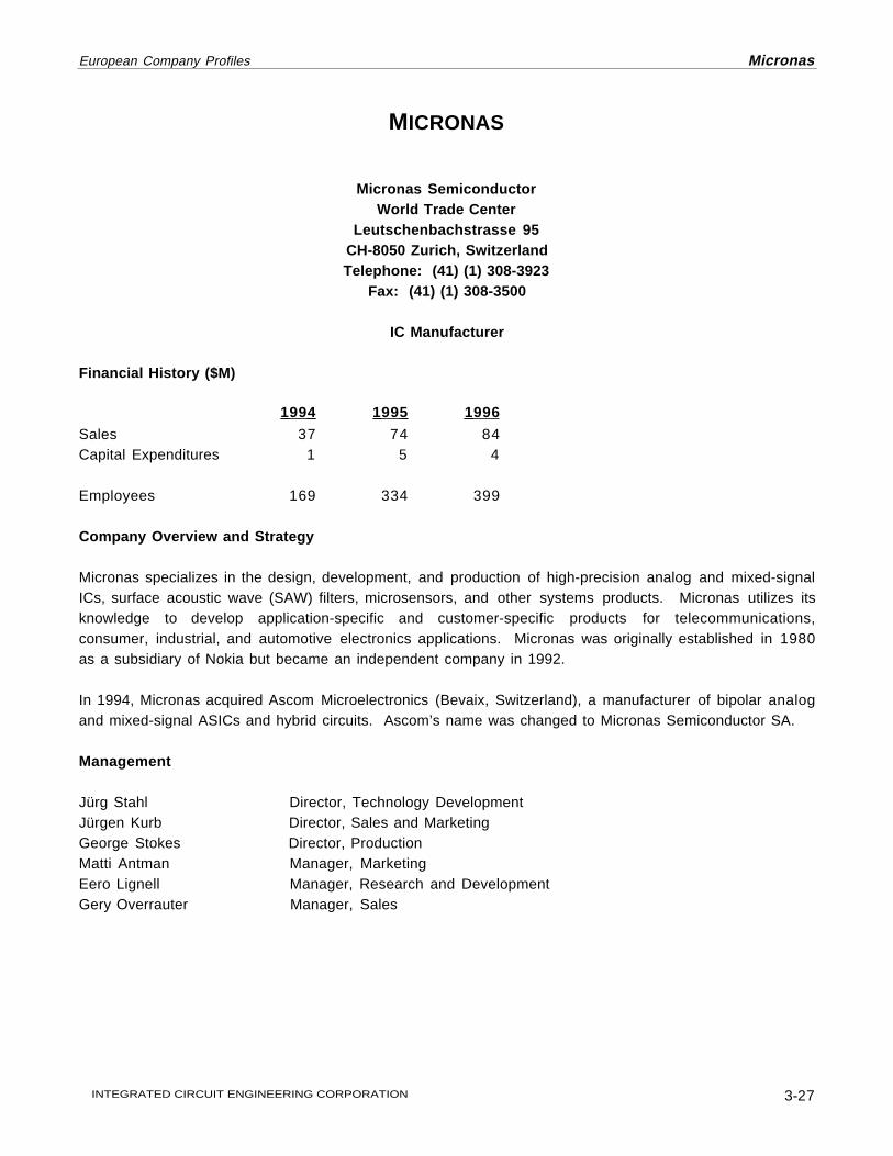
European Company Profiles Micronas
MICRONAS
Micronas SemiconductorWorld Trade Center
Leutschenbachstrasse 95CH-8050 Zurich, SwitzerlandTelephone: (41) (1) 308-3923
Fax: (41) (1) 308-3500
IC Manufacturer
Financial History ($M)
1994 1995 1996
Sales 37 74 84Capital Expenditures 1 5 4
Employees 169 334 399
Company Overview and Strategy
Micronas specializes in the design, development, and production of high-precision analog and mixed-signalICs, surface acoustic wave (SAW) filters, microsensors, and other systems products. Micronas utilizes itsknowledge to develop application-specific and customer-specific products for telecommunications,consumer, industrial, and automotive electronics applications. Micronas was originally established in 1980as a subsidiary of Nokia but became an independent company in 1992.
In 1994, Micronas acquired Ascom Microelectronics (Bevaix, Switzerland), a manufacturer of bipolar analogand mixed-signal ASICs and hybrid circuits. Ascom’s name was changed to Micronas Semiconductor SA.
Management
Jürg Stahl Director, Technology DevelopmentJürgen Kurb Director, Sales and MarketingGeorge Stokes Director, ProductionMatti Antman Manager, MarketingEero Lignell Manager, Research and DevelopmentGery Overrauter Manager, Sales

3-28
INTEGRATED CIRCUIT ENGINEERING CORPORATION
Micronas European Company Profiles
Products and Processes
ASIC design and production are the main strengths of Micronas. The company’s ASIC products aretargeted at mixed-signal applications in automotive, telecommunications, consumer, and industrialelectronics.
In addition to ASICs, Micronas offers ASSPs such as digital audio chips, modem ICs, watch circuits, andhigh-precision A/D and D/A converters. Other products include hybrids, surface acoustic wave (SAW) filtersfor wireless communication applications, sensor systems, ultra stable thin-film resistors and capacitors, andnon-laser trimmed converter products.
Micronas uses a proprietary molybdenum-gate bipolar-enhanced CMOS (BeCMOS) process technology.Enhancements include the integration of highly accurate thin-film resistors and capacitors as well as isolatedbipolar transistors. The process supports nominal power supply voltages between 1.2V and 40V.
Semiconductor Fabrication Facilities
Micronas OyKamreerintie 2P.O. Box 51FIN-02771 Espoo, FinlandTelephone: (358) (9) 80521Cleanroom size: 4,300 square feetCapacity (wafers/week): 2,000Wafer size: 100mmProcess: Moly-gate CMOSProducts: Mixed-signal and analog ICs, ASICs, ASSPs, foundry servicesFeature sizes: 2.0µm, 2.5µm, 4.0µm
Micronas Semiconductor SACh. Chapons-des-PresCH-2022 Bevaix, SwitzerlandTelephone: (41) (32) 847-0111Cleanroom size: 21,500 square feetCapacity (wafers/week): 2,000Wafer size: 100mmProcesses: Bipolar, moly-gate CMOS, lift-off and dry etch processesProducts: ASICs, hybrids, saw filters, pressure sensors, foundry servicesFeature size: 3.0µm

INTEGRATED CIRCUIT ENGINEERING CORPORATION 3-29
European Company Profiles Newport Wafer-Fab
NEWPORT WAFER-FAB (NWL)
Newport Wafer-Fab LimitedCardiff Road
Duffryn, NewportGwent NP9 1YJ, Wales
United KingdomTelephone: (44) (1633) 810121
Fax: (44) (1633) 810820
IC Manufacturer
Employees 480
Regional Headquarters/Representative Locations
North America: ASAT Inc. • Palo Alto, CaliforniaTelephone: (415) 969-1141 • Fax: (415) 969-6580
Company Overview and Strategy
Newport Wafer-Fab Limited (NWL) was founded as a subsidiary of Hong Kong-based QPL InternationalHoldings Limited in 1992 when QPL acquired the fab facility originally established in 1982 by SGS-Thomsonsubsidiary INMOS. QPL is a growing group of companies dedicated to providing manufacturing services tothe semiconductor industry.
NWL is a pure wafer foundry and is focused on becoming Europe’s largest contract wafer manufacturingoperation. The company produces CMOS ICs primarily for telecommunications, industrial, and non-volatilememory applications, with particular expertise in mixed-signal designs. NWL is located near ASAT UK, asister company within QPL, which offers assembly and test capabilities, thus offering total turnkeyoperations.
Management
Steve Byars Chief Executive OfficerJohn Elder Director, OperationsGareth Jones Director, Sales and Marketing
Products and Processes
NWL’s foundry services consist of two dedicated fabs with double- and triple-level metal, single- and double-level poly CMOS wafer fabrication down to 0.5µm feature sizes. With the completion of Fab 3 in 3Q97, thecompany will offer 200mm wafer capacity in 0.5µm CMOS, moving to 0.35µm.
3-30
INTEGRATED CIRCUIT ENGINEERING CORPORATION
Newport Wafer-Fab European Company Profiles
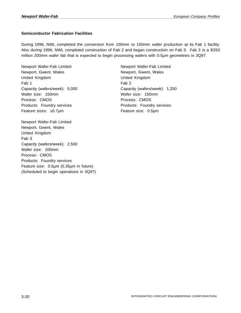
Semiconductor Fabrication Facilities
During 1996, NWL completed the conversion from 100mm to 150mm wafer production at its Fab 1 facility.Also during 1996, NWL completed construction of Fab 2 and began construction on Fab 3. Fab 3 is a $350million 200mm wafer fab that is expected to begin processing wafers with 0.5µm geometries in 3Q97.
Newport Wafer-Fab Limited Newport Wafer-Fab LimitedNewport, Gwent, Wales Newport, Gwent, WalesUnited Kingdom United KingdomFab 1 Fab 2Capacity (wafers/week): 5,000 Capacity (wafers/week): 1,250Wafer size: 150mm Wafer size: 150mmProcess: CMOS Process: CMOSProducts: Foundry services Products: Foundry servicesFeature sizes: ≥0.7µm Feature size: 0.5µm
Newport Wafer-Fab LimitedNewport, Gwent, WalesUnited KingdomFab 3Capacity (wafers/week): 2,500Wafer size: 200mmProcess: CMOSProducts: Foundry servicesFeature size: 0.5µm (0.35µm in future)(Scheduled to begin operations in 3Q97)

INTEGRATED CIRCUIT ENGINEERING CORPORATION 3-31
European Company Profiles Philips Semiconductors
PHILIPS SEMICONDUCTORS
Philips Semiconductors BVBuilding BAE2 19
P.O. Box 2185600MD Eindhoven, The Netherlands
Telephone: (31) (40) 723-520Fax: (31) (40) 723-085
Web Site: www.semiconductors.philips.com
IC Manufacturer
Regional Headquarters/Representative Locations
North America: Philips Semiconductors • Sunnyvale, CaliforniaTelephone: (408) 991-2000 • Fax: (408) 991-2311
Japan: Philips Semiconductors • Minato-ku, Tokyo, JapanTelephone: (81) (3) 3740-5130 • Fax: (81) (3) 3740-5077
Asia-Pacific: Philips Taiwan Ltd. • Taipei, TaiwanTelephone: (886) (2) 382-4443 • Fax: (886) (2) 382-4444
Financial History, Fiscal Year Ends December 31
1992 1993 1994 1995 1996
Corporate (NLG in millions)Sales NLG58,527 NLG58,825 NLG60,977 NLG64,462 NLG69,195Net Income NLG(900) NLG1,965 NLG2,049 NLG2,684 NLG723
Semiconductor Business ($M)Sales $2,055 $2,250 $2,866 $3,994 $4,196 IC Sales $1,480 $1,640 $2,106 $2,936 $3,253 Discrete Sales $575 $610 $760 $1,058 $943R&D Expenditures $725 $760Capital Expenditures $140 $134 $320 $750 $510
Employees 20,000 19,000 21,000 26,000 26,000
3-32
INTEGRATED CIRCUIT ENGINEERING CORPORATION
Philips Semiconductors European Company Profiles
Company Overview and Strategy
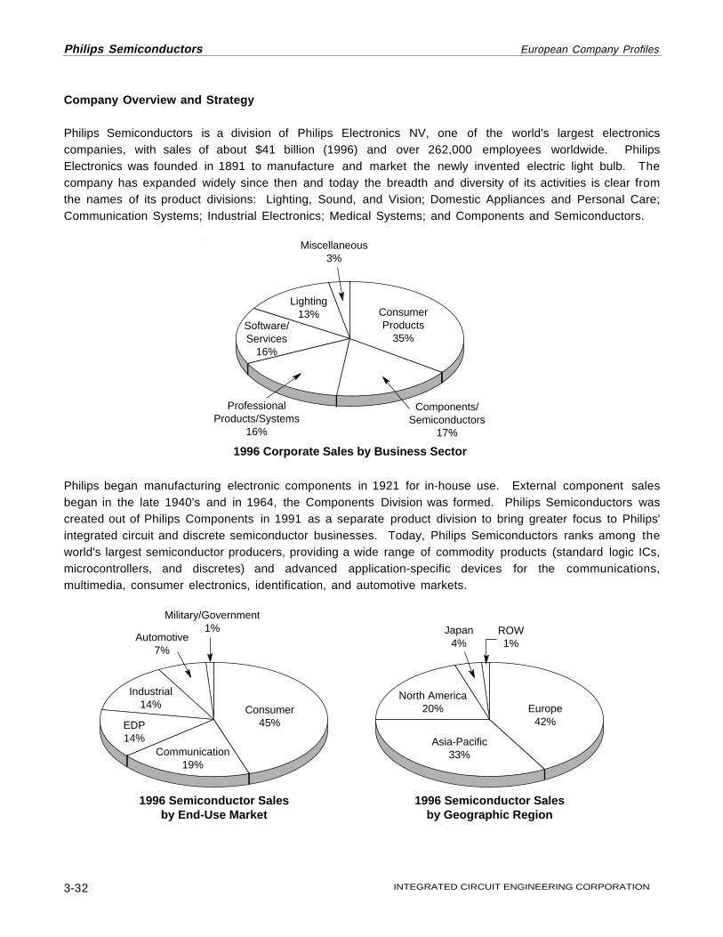
Philips Semiconductors is a division of Philips Electronics NV, one of the world's largest electronicscompanies, with sales of about $41 billion (1996) and over 262,000 employees worldwide. PhilipsElectronics was founded in 1891 to manufacture and market the newly invented electric light bulb. Thecompany has expanded widely since then and today the breadth and diversity of its activities is clear fromthe names of its product divisions: Lighting, Sound, and Vision; Domestic Appliances and Personal Care;Communication Systems; Industrial Electronics; Medical Systems; and Components and Semiconductors.
ConsumerProducts
35%
Miscellaneous3%
1996 Corporate Sales by Business Sector
ProfessionalProducts/Systems
16%
Components/Semiconductors
17%
Lighting13%
Software/Services
16%
Philips began manufacturing electronic components in 1921 for in-house use. External component salesbegan in the late 1940's and in 1964, the Components Division was formed. Philips Semiconductors wascreated out of Philips Components in 1991 as a separate product division to bring greater focus to Philips'integrated circuit and discrete semiconductor businesses. Today, Philips Semiconductors ranks among theworld's largest semiconductor producers, providing a wide range of commodity products (standard logic ICs,microcontrollers, and discretes) and advanced application-specific devices for the communications,multimedia, consumer electronics, identification, and automotive markets.
Consumer45%
Military/Government1%
1996 Semiconductor Salesby End-Use Market
Industrial14%
EDP14%
Communication19%
Automotive7%
Europe42%
Japan4%
1996 Semiconductor Salesby Geographic Region
Asia-Pacific33%
North America20%
ROW1%

INTEGRATED CIRCUIT ENGINEERING CORPORATION 3-33
European Company Profiles Philips Semiconductors
Philips Semiconductors is structured into four business groups: Consumer ICs, Communications andMultimedia, Auto/ID/Storage and Logic ICs, and Discrete Semiconductors. Approximately 15 percent ofPhilips Semiconductors’ devices are sold to other business sectors within Philips.
Building on its strategy to establish itself as a leader in the multimedia market, Philips Semiconductorsacquired the multimedia IC business of Western Digital Corporation in November 1995. Under terms of theagreement, Philips acquired all of the assets of Western Digital’s Multimedia Products Unit, which includedthe RocketCHIP family of ICs and the Paradise graphics accelerator cards (Philips shut down the cardbusiness in 1996). In addition, Philips and German software vendor Spea Software AG forged anagreement aimed at jointly developing high performance 3D multimedia ICs for PCs and game equipment.
Management
Arthur van der Poel Chairman and Chief Executive Officer, Philips SemiconductorsStuart McIntosh Chief Operations OfficerRoss Anderson Vice President and GM, Auto/ID/Storage and Logic IC Business GroupGuenther Dengel Vice President and GM, Consumer IC Business GroupLeon Husson Vice President and GM, Discrete Semiconductor Business GroupCees Jan Kooman Vice President and GM, Communications and Multimedia Business GroupWalter Conrads Director, International Sales and Marketing
Products and Processes
Philips' semiconductor products are split up by business group below.
Consumer IC Group Auto/ID/Storage and Logic IC Group• digital audio circuits • automotive circuits• radio/TV/VCR signal processing ICs • data communications chips• motor drive/control circuits • RF/telecom ICs• data conversion devices • standard logic devices• monitor ICs • PLDs
Communications and Multimedia Group Discrete Semiconductors Group• microcontrollers • power MOSFETs• telecommunications devices • power transistors• digital video/audio circuits • amplifiers

3-34
INTEGRATED CIRCUIT ENGINEERING CORPORATION
Philips Semiconductors European Company Profiles
MOS MEMORY ANALOG
DRAM ✔ Amplifier
SRAM ✔ Interface
Flash Memory ✔ Consumer/Automotive
EPROM ✔ Voltage Regulator/Reference
ROM ✔ Data Conversion
EEPROM ✔ Comparator
Other (Including Non-Volatile RAM) ✔ Other (Includes Telecom)
MOS LOGIC DIGITAL BIPOLAR
✔ General Purpose Logic ✔ Bipolar Memory
Gate Array ✔ General Purpose Logic
Standard Cell Gate Array/Standard Cell
✔ Field Programmable Logic ✔ Field Programmable Logic
✔ Other Special Purpose Logic Other Special Purpose Logic
MPU/MCU/MPR
MOS MICROCOMPONENT
MPU OTHER
✔ MCU Full Custom IC
✔ MPR ✔ Discrete
✔ DSP Optoelectronic
Multimedia ICs
Philips sees multimedia as a key growth area. The company began marketing MPEG-1 and MPEG-2audio/video compression chips in 1995. Through its acquisition of Western Digital’s multimedia IC business,Philips now offers leading-edge 3D graphics coprocessors and full-motion video/graphics accelerators. ForCD systems, Philips provides devices for high-speed CD-ROM drives and Video-CD and CD-Recordable/Erasable systems.
Philips also began selling its powerful programmable digital signal processor, named TriMedia, in late 1996.The first generation single-chip TriMedia media processor has the power (up to four billion operations persecond) to process audio, video, graphics, and communications data concurrently. Specifically designed formultimedia processing, the TriMedia processor uses a VLIW (very long instruction word) architecture andinnovative scheduling compiler to process multiple operations in a single clock cycle. The TriMedia family ofprocessors also offers an open development environment.
Audio and Video ICs
Philips offers over 200 ICs for television and video applications, such as wide-screen TVs, surround-soundfunctions, video cameras, VCRs, and monitors. The company also offers a wide range of digital-to-analog(D/A) and analog-to-digital (A/D) converters, power amplifiers, and DSPs for audio processing.

INTEGRATED CIRCUIT ENGINEERING CORPORATION 3-35
European Company Profiles Philips Semiconductors
Telecommunications ICs
The company’s telecommunications products are focused on five key segments—multimediacommunications, cellular and cordless telephones, portable mobile radios, pagers, and satellitecommunications. Philips also provides 8-bit and 32-bit microcontrollers and other ICs for datacommunications applications.
Identification ICs
For identification applications, Philips’ core skills are in encryption coding, sensor interfaces, RF coupling, andsmartcards.
Automotive ICs
Philips’ automotive semiconductors include devices for ABS, airbag, traction control, comfort control, enginemanagement, in-car information, communication, and entertainment applications.
Microcontrollers
Philips is a leader in the 80C51 microcontroller business with devices operating down to 1.8V. In 1994, thecompany extended the venerable 80C51 to the 16-bit level. The 16-bit 80C51XA microcontrollers are saidto provide up to 10 times the performance of the 8-bit 80C51.
Logic ICs
Philips is one of the world’s leading suppliers of general-purpose logic ICs, with a variety of 3V, 5V, mixed-voltage, high-speed, CMOS, bipolar, and BiCMOS devices. The company has also been a long-timeparticipant in the PLD market. It offers simple PLDs (SPLDs) and complex PLDs (CPLDs), including its newCoolRunner™ line of low-power (3.3V), high-performance CPLDs based on a design technique Philips callsFast Zero Power (FZP).
Discrete Semiconductors
Philips is one of the world’s largest producers of discrete semiconductors with its products including smallsignal diodes and transistors, power transistors, RF and microwave diodes, transistors and modules, andsensors.
Analog31%
1996 Semiconductor Salesby Device Type
MOS MCU/MPR26%
MOS Logic18%
Discrete23%
Bipolar Digital2%

3-36
INTEGRATED CIRCUIT ENGINEERING CORPORATION
Philips Semiconductors European Company Profiles
The technologies used in the manufacture of Philips' semiconductors include advanced bipolar, CMOS,BiCMOS, and BCDMOS including submicron. Philips’ leading edge CMOS process technologies include its0.5µm three-layer-metal C100 process and its 0.35µm C075 process, which is available with four or fivelayers of metal. Many new, advanced product lines are based on the company's proprietary QUBiC BiCMOSprocess, which is currently at the 0.8µm geometry level.
Semiconductor Fabrication Facilities
Philips Semiconductors Philips SemiconductorsGerstweg 2 Gerstweg 2Building ANO 121 Building ANO 1216534 AE Nijmegen, The Netherlands 6534 AE Nijmegen, The NetherlandsMOS2 MOS3Telephone: (31) (80) 532-544 Telephone: (31) (80) 532-544Cleanroom size: 34,440 square feet, Class 10 Cleanroom size: 32,300 square feet, Class 10Capacity (wafers/week): 10,250 Capacity (wafers/week): 5,000Wafer size: 100mm Wafer size: 150mmProcesses: CMOS, DMOS Processes: CMOS, BiCMOSProducts: Logic ICs Products: Logic and analog ICs, MCUsFeature sizes: 1.2µm, 2.0µm, 3.0µm Feature sizes: 0.6µm, 0.7µm, 0.8µm
Philips Semiconductors Philips SemiconductorsGerstweg 2 Gerstweg 2Building ANO 121 Building ANO 1216534 AE Nijmegen, The Netherlands 6534 AE Nijmegen, The NetherlandsTelephone: (31) (80) 532-544 Telephone: (31) (80) 532-544MOS4YOU (Yield Output Utilization) CIC/AN FabCleanroom size: 74,270 square feet, Class 0.1-1 Cleanroom size: 48,440 square feet, Class 10Capacity (wafers/week): 4,600 Capacity (wafers/week): 7,500Wafer size: 200mm Wafer size: 125mmProcess: CMOS Processes: Bipolar, BiCMOSProducts: Consumer and communications ICs Products: Digital bipolar and analog ICsFeature sizes: 0.35µm, 0.5µm Feature sizes: 1.75µm, 3.0µm
Philips Semiconductors Philips SemiconductorsGerstweg 2 P.O. Box 10Building ANO 121 Electronicaweg 16534 AE Nijmegen, The Netherlands 9500AA Stadskanaal, The NetherlandsTelephone: (31) (80) 532-544 Telephone: (31) (599) 032330Cleanroom size: 32,300 square feet, Class 1,000 Cleanroom size: 26,900 square feet, Class 10,000Capacity (wafers/week): 3,750 Capacity (wafers/week): 17,500Wafer size: 100mm Wafer size: 100mmProcesses: MOS, bipolar Process: BipolarProducts: Discretes Products: DiscretesFeature sizes: 0.7µm-100µm Feature sizes: 1.0µm, 3.0µm
INTEGRATED CIRCUIT ENGINEERING CORPORATION 3-37
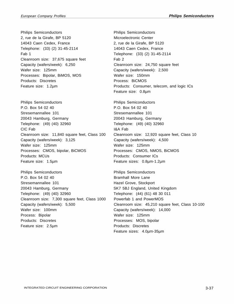
European Company Profiles Philips Semiconductors
Philips Semiconductors Philips Semiconductors2, rue de la Girafe, BP 5120 Microelectronic Center14043 Caen Cedex, France 2, rue de la Girafe, BP 5120Telephone: (33) (2) 31-45-2114 14043 Caen Cedex, FranceFab 1 Telephone: (33) (2) 31-45-2114Cleanroom size: 37,675 square feet Fab 2Capacity (wafers/week): 6,250 Cleanroom size: 24,750 square feetWafer size: 125mm Capacity (wafers/week): 2,500Processes: Bipolar, BiMOS, MOS Wafer size: 150mmProducts: Discretes Process: BiCMOSFeature size: 1.2µm Products: Consumer, telecom, and logic ICs
Feature size: 0.8µm
Philips Semiconductors Philips SemiconductorsP.O. Box 54 02 40 P.O. Box 54 02 40Stresemannallee 101 Stresemannallee 10120043 Hamburg, Germany 20043 Hamburg, GermanyTelephone: (49) (40) 32960 Telephone: (49) (40) 32960CIC Fab I&A FabCleanroom size: 11,840 square feet, Class 100 Cleanroom size: 12,920 square feet, Class 10Capacity (wafers/week): 3,125 Capacity (wafers/week): 4,500Wafer size: 125mm Wafer size: 125mmProcesses: CMOS, bipolar, BiCMOS Processes: CMOS, NMOS, BiCMOSProducts: MCUs Products: Consumer ICsFeature size: 1.5µm Feature sizes: 0.8µm-1.2µm
Philips Semiconductors Philips SemiconductorsP.O. Box 54 02 40 Bramhall More LaneStresemannallee 101 Hazel Grove, Stockport20043 Hamburg, Germany SK7 5BJ England, United KingdomTelephone: (49) (40) 32960 Telephone: (44) (61) 48 30 011Cleanroom size: 7,300 square feet, Class 1000 Powerfab 1 and PowerMOSCapacity (wafers/week): 5,500 Cleanroom size: 45,210 square feet, Class 10-100Wafer size: 100mm Capacity (wafers/week): 14,000Process: Bipolar Wafer size: 125mmProducts: Discretes Processes: MOS, bipolarFeature size: 2.5µm Products: Discretes
Feature sizes: 4.0µm-35µm

3-38
INTEGRATED CIRCUIT ENGINEERING CORPORATION
Philips Semiconductors European Company Profiles
Crolles Joint Research Center Philips SemiconductorsCrolles, France 811 East Arques AvenueCleanroom size: 21,340 square feet Sunnyvale, California 94088-3409Wafer size: 200mm Telephone: (408) 991-2000Processes: CMOS, BiCMOS Fab 1Products: R&D Cleanroom size: 32,300 square feet, Class 100Feature sizes: 0.25µm-0.8µm Capacity (wafers/week): 5,750(R&D facility jointly operated by Philips, Wafer size: 100mmSGS-Thomson, and CNET) Process: Bipolar
Products: Linear ICsFeature sizes: 2.0µm-4.0µm
Philips Semiconductors Philips Semiconductors9201 Pan American Expressway N.E. 9201 Pan American Expressway N.E.Albuquerque, New Mexico 87184 Albuquerque, New Mexico 87184Telephone: (505) 822-7000 Telephone: (505) 822-7000Fab 22 Fab 23Cleanroom size: 32,300 square feet, Class 100 Cleanroom size: 43,050 square feet, Class 10Capacity (wafers/week): 8,250 Capacity (wafers/week): 4,175Wafer sizes: 100mm Wafer size: 150mmProcesses: CMOS, bipolar Processes: CMOS, BiCMOSProducts: MCUs Products: MCUs, PLDs, ASICsFeature size: 1.0µm Feature sizes: 0.65µm, 0.8µm (0.5µm in 1997)
SubMicron Semiconductor Technologies GmbH (SMST)Schoenaicherstrasse 220Boeblingen Hulb, GermanyCleanroom size: 107,640 square feet, Class 1Capacity (wafers/week): 4,000Wafer size: 200mmProcess: CMOSProducts: DRAMs, logic ICsFeature size: 0.65µm(Joint venture with IBM Microelectronics.See Key Agreements.)
Philips also owns 34 percent of Taiwan Semiconductor Manufacturing Co. (TSMC) and 38 percent ofAdvanced Semiconductor Manufacturing Corp. of Shanghai (ASMC). For data on the fab facilities of ASMCand TSMC, see the profiles of each in this publication.
Philips has 11 assembly/test facilities located around the world. These are located in The Netherlands,England, Belgium, France, Germany, Thailand, China, Malaysia, Hong Kong, Korea, and the Philippines.

INTEGRATED CIRCUIT ENGINEERING CORPORATION 3-39
European Company Profiles Philips Semiconductors
Key Agreements
• Philips licensed the ARM7 32-bit microprocessor core from Advanced RISC Machines in early 1997.
• In April 1996, Philips announced a wafer sourcing agreement with TriQuint Semiconductor. Under theagreement, GaAs ICs developed at Philips Microwave Limeil, France, will be produced by TriQuint andthen marketed only by Philips.
• Philips revealed in 1995, a partnership with German software vendor Spea Software AG to jointly develophigh performance 3D multimedia ICs for PC and game equipment applications.
• In 1994, Philips agreed with IBM Microelectronics to form a joint venture to manufacture ICs at IBM's fabfacility in Boeblingen Hulb, Germany. Philips holds 51 percent and IBM 49 percent of the new company,called SubMicron Semiconductor Technologies GmbH (SMST). SMST is supplying products solely to IBMand Philips, manufacturing DRAMs for IBM and logic ICs for Philips. Separately, Philips acquired therights to IBM’s 16M DRAM technology for embedded applications. Embedded DRAM products will alsobe produced by SMST.
• Philips formed a joint venture in China in 1994 with Northern Telecom and the Chinese government. Thenew company, called Advanced Semiconductor Manufacturing Corp. (ASMC), took over Philips' wafer fabin China. In 1996, the partners completed the installation of a new 150mm wafer line for processing0.8µm BiCMOS and 1.0µm CMOS circuits.
• Philips Semiconductors has a technology partnership with TI-subsidiary Silicon Systems concerning diskdrive ICs.
• Philips, TI, and Hitachi formed a pact in 1993 covering joint development and alternate sourcing ofFutureBus and BiCMOS logic IC products.
• Philips extended its patent cross-license agreement with Intel to include all of each others semiconductordevices except certain proprietary Intel MPUs and Philips video products. The agreement is now validthrough the year 2000. In addition, the two companies established an agreement to develop a newfamily of 8-bit MCUs, based on an upgraded 80C51 core.
• Philips has a license from Silicon Graphics for 32-bit and 64-bit Mips RISC core microprocessortechnologies. Philips is embedding the Mips R4000 cores in chips for communications and multimediaapplications. Philips obtained Mips R3000 microprocessor technology in 1994 when it acquired HDLSystems.

3-40
INTEGRATED CIRCUIT ENGINEERING CORPORATION
Seagate Microelectronics European Company Profiles
SEAGATE MICROELECTRONICS
Seagate Microelectronics LimitedMacintosh RoadKirkton Campus
Livingston EH54 7BW, ScotlandTelephone: (44) (1506) 416416
Fax: (44) (1506) 413526
Captive IC Manufacturer
Regional Headquarters/Representative Locations
North America: Seagate Technology • Scotts Valley, CaliforniaTelephone: (408) 438-6550
Company Overview and Strategy
Seagate Microelectronics was established in 1987 to supply integrated circuits to its parent SeagateTechnology, a $3 billion supplier of computer disk drives and related products.
Management
Gordon Hutchison Managing DirectorAdolf Belka Senior Director, TechnologyChris Gater Senior Director, Design & DevelopmentJohn Chisholm Director, QualityAlan Spiers Director, ManufacturingMargaret Henaughen Manager, Human ResourcesBill Somerville Manager, FacilitiesAlistair Dick Financial Controller
Products and Processes
Seagate Microelectronics Limited designs, develops, and manufactures mixed-signal ICs for signalprocessing, power management, and power control using bipolar and BiCMOS process technologies withminimum design rules down to 1.0µm.

INTEGRATED CIRCUIT ENGINEERING CORPORATION 3-41
European Company Profiles Seagate Microelectronics
Semiconductor Fabrication Facilities
Seagate Microelectronics Ltd.Macintosh RoadKirkton CampusLivingston EH54 7BW, ScotlandCleanroom size: 15,500 square feetCapacity (wafers/week): 2,000Wafer size: 100mmProcesses: Bipolar, BiCMOSProducts: Mixed-signal ICsFeature sizes: 1.0µm-3.0µm

3-42
INTEGRATED CIRCUIT ENGINEERING CORPORATION
SGS-Thomson Microelectronics European Company Profiles
SGS-THOMSON MICROELECTRONICS
SGS-Thomson MicroelectronicsTechnoparc du Pays de Gex
165 rue Edouard Branly, BP 11201630 Saint Genis Pouilly, France
Telephone: (33) (4) 50-40-26-40Fax: (33) (4) 50-40-28-60Web Site: www.st.com
IC Manufacturer
Regional Headquarters/Representative Locations
North America: SGS-Thomson Microelectronics Inc. • Carrollton, TexasTelephone: (214) 466-6000 • Fax: (214) 466-8130
Japan: SGS-Thomson Microelectronics K.K. • Minato-ku, Tokyo, JapanTelephone: (81) (3) 3280-4121 • Fax: (81) (3) 3280-4131
Asia-Pacific: SGS-Thomson Microelectronics Asia Pacific Pte., Ltd. • SingaporeTelephone: (65) 482-1411 • Fax: (65) 482-0240
Financial History ($M), Fiscal Year Ends December 31
1992 1993 1994 1995 1996
Sales 1,568 2,038 2,640 3,554 4,122 IC Sales 1,241 1,642 2,207 2,964 3,522 Discrete Sales 327 396 433 590 600Net Income 3 160 362 526 625R&D Expenditures 261 271 338 440 532Capital Expenditures 196 446 780 1,002 1,125
Employees 17,000 20,000 21,000 25,000 26,000
Company Overview and Strategy
SGS-Thomson Microelectronics (ST) was established in 1987 as a result of the merging of SGSMicroelettronica of Italy and Thomson Semiconducteurs of France, two companies that each had almost 30years of experience in the field of semiconductors at the time of the merger.

INTEGRATED CIRCUIT ENGINEERING CORPORATION 3-43
European Company Profiles SGS-Thomson Microelectronics
SGS-Thomson Microelectronics designs, develops, manufactures, and markets a broad range of integratedcircuits and discrete devices for use in a wide variety of microelectronics applications, includingtelecommunications systems, computer systems, consumer products, automotive products, and industrialautomation and control systems.
SGS-Thomson is a leading supplier in many semiconductor markets, including power ICs, analog and mixed-signal ICs, MPEG decoder ICs, smartcard ICs, and EPROMs.
Computer27%
1996 Sales by End-Use Market
Industrial19%
Telecom22%
Consumer22%
Automotive 10%
Europe44%
Japan 6%
1996 Sales by Geographic Region
Asia-Pacificand ROW
27%
Americas23%
With respect to its products, ST is organized into five principal groups: the Dedicated Products Group (DPG),the Discrete and Standard ICs Group (DSG), the Memory Products Group (MPG), the ProgrammableProducts Group (PPG), and the New Ventures Group (NVG).
DPG43%
PPG17%
1996 Sales by Product Group
DSG19%
MPG18%
NVG3%
• The Dedicated Products Group produces application-specific semiconductor products using advancedbipolar, CMOS, BiCMOS, mixed-signal, and power technologies. These products include imageprocessing devices and telecommunications chips.
• The Discrete and Standard ICs Group produces discrete power devices, standard linear and logic ICs,and radio frequency (RF) products.
• The Memory Products Group produces a broad range of memory ICs, including EPROMs, flashmemories, EEPROMs, SRAMs, and chips for smartcards.

3-44
INTEGRATED CIRCUIT ENGINEERING CORPORATION
SGS-Thomson Microelectronics European Company Profiles
• The Programmable Products Group produces microcomponents (including MCUs, MPUs, and DSPs),digital and mixed-signal semicustom devices, PC graphics chips, and multimedia acceleration ICs.
• The New Ventures Group identifies and develops new business opportunities to complement thecompany’s existing businesses and exploit its technological know-how, manufacturing capabilities, andglobal marketing team. Its initial activities have been focused on the manufacture and sale of x86 MPUsdesigned by Cyrix Corporation.
Management
Pasquale Pistorio President and Chief Executive OfficerLaurent Bosson Vice President, Front End ManufacturingCarlo Bozotti Vice President, European Region and HeadquartersSalvatore Castorina Vice President, Discrete and Standard ICs GroupMurray Duffin Vice President, Total Quality ManagementAlain Dutheil Vice President, Strategic Planning and Human ResourcesEnnio Filauro Vice President, Memory Products GroupPhillippe Geyres Vice President, Programmable Products GroupMaurizio Ghirga Vice President and Chief Financial OfficerJ.C. Marquet Vice President, Asia/Pacific OperationsPier Angelo Martinotti Vice President, New Ventures GroupJoel Monnier Vice President, Central Research and DevelopmentPiero Mosconi Vice President and TreasurerRichard Pieranunzi Vice President, Corporate Marketing and President, American RegionAldo Romano Vice President, Dedicated Products GroupGiordano Seragnoli Vice President, Back End Manufacturing and SubsystemsKeizo Shibata Vice President, Japan Region
Products and Processes
SGS-Thomson produces a wide range of discrete semiconductor devices and integrated circuits usingadvanced bipolar, BiCMOS, CMOS, and mixed technologies. SGS-Thomson is particularly strong in thetelecommunications, automotive, and industrial sectors, reflecting its strengths in power integrated circuitsand power transistors.
Complementing its power products, SGS-Thomson offers a wide range of digital and mixed-signal circuits,including microcontrollers and processors, EPROMs, EEPROMs, flash memories, high-performance SRAMs,telecommunications circuits, graphics processors, and image compression devices.
In early 1997, the company introduced the first device from its Omega line of system-on-a-chip devices thatwill feature 1M of embedded DRAM at first, moving to 4M later. Using embedded DRAM technologylicensed from U.S.-based Artisan Components, the introduction marks the first time SGS-Thomson hasfabricated DRAM circuitry on ICs in any quantity. In a separate announcement, ST unveiled another devicecalled the Chameleon. The Chameleon device is a 64-bit proprietary, multimedia microprocessor that will beused in an automotive system-on-a-chip device that will include navigation, global positioning system, GSMwireless phone, DVD audio, and radio-link data-system functions.

INTEGRATED CIRCUIT ENGINEERING CORPORATION 3-45
European Company Profiles SGS-Thomson Microelectronics
MOS MEMORY ANALOG
DRAM ✔ Amplifier
✔ SRAM Interface
✔ Flash Memory ✔ Consumer/Automotive
✔ EPROM ✔ Voltage Regulator/Reference
ROM ✔ Data Conversion
✔ EEPROM ✔ Comparator
✔ Other (Including Non-Volatile RAM) ✔ Other (Includes Telecom)
MOS LOGIC DIGITAL BIPOLAR
✔ General Purpose Logic Bipolar Memory
✔ Gate Array ✔ General Purpose Logic
✔ Standard Cell Gate Array/Standard Cell
Field Programmable Logic Field Programmable Logic
Other Special Purpose Logic Other Special Purpose Logic
MPU/MCU/MPR
MOS MICROCOMPONENT
✔ MPU OTHER
✔ MCU Full Custom IC
✔ MPR ✔ Discrete
✔ DSP Optoelectronic
Details concerning ST’s semiconductor products are given below.
Dedicated Products
• Telecom and Data Communications ICs—includes network ICs, modem ICs, switching ICs, and linear ICs.• Automotive ICs—includes linear ICs, controllers, instrumentation circuits, and audio ICs.• Industrial ICs—includes power controllers and motor drivers.• Consumer ICs—includes audio ICs, digital compression circuits, and television circuits.• Computer ICs—includes display circuits and PC graphics devices.
Standard Circuits
• Processors and Peripherals—includes the Cyrix-designed ST486, ST5x86, and ST6x86 families of MPUs;microcontrollers in 4-bit, 8-bit, 16-bit, and 32-bit configurations; DSPs; fuzzy logic processors; peripheralprotection circuits; Transputer processors; and video compression circuits.
• Memories and Smartcard Products—includes UVEPROMs and OTPROMs in densities from 16K to 16M;flash memories in densities from 256K to 16M; 16K and 64K parallel EEPROMs; serial EEPROMs indensities from 256bit to 256K; synchronous and asynchronous fast CMOS SRAMs; timekeeper andzeropower SRAMs; and memory-based smartcard ICs. Low voltage versions of many of the memory ICsare available.
• Standard Linear ICs—includes voltage regulators, comparators, amplifiers, timers, data converters, andother standard linear ICs in advanced bipolar, CMOS, and BiCMOS technologies.
• Logic Circuits—includes CMOS, high-speed CMOS, and low-power schottky general-purpose logic ICs.

3-46
INTEGRATED CIRCUIT ENGINEERING CORPORATION
SGS-Thomson Microelectronics European Company Profiles
Semicustom Circuits
• Digital Circuits—includes high-performance CMOS standard cell ASICs, sea-of-gates structured arrays,sea-of-gates arrays with embedded functions, and sea-of-gates continuous arrays.
• Analog and Mixed-Signal Circuits—includes analog and mixed-signal CMOS and BiCMOS standard cells.
Discrete Devices
• Transistors, thyristors, diodes, and protection devices.
RF and Microwave Devices
• Silicon power transistors and hybrid power modules.
Semiconductor Fabrication Facilities
SGS-Thomson announced plans to open one new 200mm wafer production facility each year between 1996and 2000. Following its plan, the company’s Phoenix, Arizona, facility began volume production in 1996 andits Catania facility will begin volume production in 1997. ST is currently building a new $800 million 200mmwafer fab at its site in Rousset, France, for the production of microcontrollers, non-volatile memories, andother devices with geometries of 0.5µm and below. The so-called Rousset 2000 plant will have the capacityto process 5,000 wafers per week, with the first chips scheduled for early 1998.
The company is looking to build at least two more 200mm wafer fabs by the end of the decade, one ofwhich will be located in Italy and the other at the company’s existing site in Singapore. The 200mm fab inSingapore is expected to be up and running by 1999 with a throughput of 6,250 wafers per week producedin 0.25µm technology.
SGS-Thomson Microelectronics S.A. SGS-Thomson Microelectronics S.A.3 rue de Suisse, BP 4199 17 Avenue des Martyrs, BP 21735041 Rennes Cedex, France 38019 Grenoble Cedex, FranceTelephone: (33) (2) 99-26-4800 Telephone: (33) (4) 76-58-5000Cleanroom size: 27,500 square feet Cleanroom size: 26,400 square feetCapacity (wafers/week): 3,500 Capacity (wafers/week): 5,000Wafer size: 125mm (upgrade to 150mm in 1997) Wafer size: 100mmProcesses: Bipolar, BiCMOS Processes: Bipolar, MOSProducts: Hi-Rel/aerospace and other ICs Products: Audio, telecom, and video ICsFeature size: 2.5µm Feature sizes: 1.2µm-3.0µm
SGS-Thomson Microelectronics S.A. SGS-Thomson Microelectronics S.A.Zone Industrielle Peynier-Rousset, BP 2 Zone Industrielle Peynier-Rousset, BP 213790 Rousset, France 13790 Rousset, FranceTelephone: (33) (4) 42-25-8800 Telephone: (33) (4) 42-25-8800Cleanroom size: 50,500 square feet Capacity (wafers/week): 5,000Capacity (wafers/week): 6,500 Wafer size: 200mmWafer size: 150mm Process: CMOSProcesses: CMOS, NMOS Products: MCUs, EEPROMsProducts: Microcomponents, EPROMs, EEPROMs Feature sizes: 0.35µm, 0.5µm (0.25µm capable)Feature sizes: 1.0µm-1.5µm (Scheduled to begin production in early 1998)

INTEGRATED CIRCUIT ENGINEERING CORPORATION 3-47
European Company Profiles SGS-Thomson Microelectronics
SGS-Thomson Microelectronics S.A. SGS-Thomson Microelectronics S.A.Zone Industrielle Pré Roux, BP 16 16, rue Pierre et Marie Curie, BP 015538190 Crolles, France 37001 Tours Cedex, FranceTelephone: (33) (4) 76-08-9859 Telephone: (33) (2) 47-42-4000Cleanroom size: 21,340 square feet (Class 1) Cleanroom size: 36,300 square feetCapacity (wafers/week): 5,000 Capacity (wafers/week): 15,000Wafer size: 200mm Wafer size: 100mm (upgrading to 125mm)Processes: CMOS, BiCMOS Processes: Planar and mesaProducts: ASICs and ASSPs for telecom, Products: Discretes
consumer, and auto applications, R&D Feature size: 20µmFeature sizes: 0.25µm-0.8µm
SGS-Thomson Microelectronics S.p.A. SGS-Thomson Microelectronics S.p.A.Via C Olivetti 2 Via Tolomeo 120041 Agrate (Brianzi), Italy Casella Postale n.176Telephone: (39) (60) 35-040 20100 Cornaredo MilanoCleanroom size: 114,400 square feet Castelletto, ItalyCapacity (wafers/week): 16,000 Telephone: (39) (29) 33-30Wafer size: 150mm (upgrade to 200mm by 1998) Cleanroom size: 25,300 square feetProcesses: CMOS, BiCMOS, bipolar, BCD Capacity (wafers/week): 1,250Products: Memories, ASICs, mixed-signal ICs, Wafer size: 150mm
dedicated bipolar ICs, VLSI R&D Processes: Bipolar, BCD (bipolar/CMOS/DMOS)Feature sizes: 0.5µm-2.5µm (0.35µm in 1998) Products: Smart power devices, BCD R&D
Feature sizes: 1.2µm-6.0µm
SGS-Thomson Microelectronics S.p.A. SGS-Thomson Microelectronics S.p.A.Stradale Primosole 50 Stradale Primosole 5095121 Catania, Italy 95121 Catania, ItalyTelephone: (39) (95) 59-9111 Cleanroom size: 22,000 square feetCleanroom size: 44,000 square feet Capacity (wafers/week): 5,000Capacity (wafers/week): 8,000 Wafer size: 200mmWafer size: 125mm (upgrading to 150mm) Process: CMOSProcesses: CMOS, MOS, bipolar Products: Logic ICsProducts: Logic and linear ICs, discretes Feature sizes: 0.35µm, 0.5µmFeature sizes: 3.5µm-7.0µm (Volume production scheduled for 1997)
SGS-Thomson Microelectronics Inc. SGS-Thomson Microelectronics Inc.1310 Electronics Drive 1000 East Bell RoadCarrollton, Texas 75006-5039 Phoenix, Arizona 85022Telephone: (214) 466-8844 Telephone: (602) 485-6100Cleanroom size: 15,000 square feet Cleanroom size: 75,000 square feetCapacity (wafers/week): 3,500 Capacity (wafers/week): 3,500Wafer size: 150mm Wafer size: 200mmProcesses: CMOS, BiCMOS Process: CMOSProducts: ASICs, MPUs, graphics ICs, foundry Products: MPUs, MPRs, EPROMsFeature sizes: 0.5µm-2.0µm Feature sizes: 0.35µm, 0.5µm

3-48
INTEGRATED CIRCUIT ENGINEERING CORPORATION
SGS-Thomson Microelectronics European Company Profiles
SGS-Thomson Microelectronics Inc. SGS-Thomson Microelectronics Pte. Ltd.16350 West Bernardo Drive 28 Ang Mo Kio Industrial Park 2San Diego, California 92127 Singapore 1955Telephone: (619) 485-8900 Telephone: (65) 482-1411Capacity (wafers/week): 3,600 Cleanroom size: 55,400 square feetWafer size: 100mm Capacity (wafers/week): 32,000Processes: NMOS, CMOS, BiCMOS Wafer size: 125mmProducts: Mixed-signal telecom ICs Processes: Bipolar, CMOS, NMOS, MOSFeature sizes: 0.8µm-5.0µm Products: ICs and discretes
Feature sizes: 1.0µm-3.0µm(Adding a 32,000 square-foot cleanroom for thefabrication of ICs on 200mm wafers. Scheduledto be completed in 1999.)
ST has semiconductor assembly and test facilities in Malaysia, Singapore, Morocco, Malta, and China.
Key Agreements
• In February 1997, SGS-Thomson established a relationship with Ramtron covering FRAM production.The agreement calls for SGS-Thomson to provide CMOS wafers to Ramtron, who will return the wafers toST as finished 64K FRAMs. The two companies may extend this relationship in the future to include jointfoundry or technology licensing agreements.
• SGS-Thomson established a licensing agreement with Rambus Inc. that gives ST access to Rambus’high-speed memory interface technology.
• SGS-Thomson agreed to work with Oak Technology to develop a chipset that meets the proposed AudioCodec ‘97 (AC97) standards for multimedia ICs. The specification was developed to create a standard forhigh-quality audio solutions for PCI motherboards and add-in cards.
• ST licensed the Mpact media processor technology from Chromatic Research Inc. and began samplingthe Mpact 3000 chips in November 1996.
• Samsung licensed DSP core technology from SGS-Thomson in early 1996 as part of a second-sourcingand development agreement. At first the licensing agreement will include rights to SGS-Thomson’s D95016-bit fixed-point DSP core and a second sourcing pact for ASICs based on the core. The partnership iseventually expected to include joint development of future product generations.
• SGS-Thomson and Robert Bosch signed a licensing agreement in 1995 whereby ST granted Bosch rightsto develop and manufacture smart power ICs from ST’s latest generation bipolar-CMOS-DMOS (BCD)process.
• ST and Applied Materials signed an agreement in 1995 to do cooperative work on 300mm wafermanufacturing technologies. The agreement was later extended to cover development of processingtechnologies for several device structures, including advanced interconnect and shallow trench isolationmodules for ST’s multilevel metal CMOS designs.

INTEGRATED CIRCUIT ENGINEERING CORPORATION 3-49
European Company Profiles SGS-Thomson Microelectronics
• In 1994, SGS-Thomson and Siemens announced an extension to their cooperation on Siemens’ 16-bitmicrocontrollers.
• SGS-Thomson and AMD signed an agreement in 1994 to cooperate on the definition of future flashmemory products based on AMD’s architecture.
• Cyrix extended its wafer supply agreement with SGS-Thomson in 1994. Under the new arrangement,SGS-Thomson increased the number of wafers it produces for Cyrix and is allowed to make a certainpercentage of those same wafers for itself. In addition, Cyrix granted SGS-Thomson the right to usecertain Cyrix-designed chips as part of SGS-Thomson’s ASIC libraries. SGS-Thomson is allowed toproduce and sell such ASIC products under its own name in unlimited quantities, with Cyrix receivingroyalties from the sale of the devices. Also, Cyrix has the right to sell the SGS Thomson-designed ASICsunder its own name.
• General Instrument signed a licensing agreement with ST in 1994 for GI’s DigiCipher II video compressiontechnology. The pact allows SGS-Thomson to develop “dual-mode” video decoder chips capable ofprocessing both DigiCipher and MPEG 2 video signals.
• Mitsubishi and SGS-Thomson established an agreement in 1993 on developing 16M flash memories.
• SGS-Thomson and Sanyo Electric reached an agreement in 1993 to jointly develop video compressionand modem chips for multimedia use.
• SGS-Thomson transferred its 1.2µm BiCMOS process technology to Seagate Microelectronics' fab facilityin Livingston, Scotland, in 1993. SGS-Thomson's fab in Grenoble, France, became a foundry for devicedesigns covered under the agreement with Seagate.
• SGS-Thomson entered into a strategic alliance with Northern Telecom in 1993 involving technologydevelopment and manufacturing of custom telecommunications ICs. As part of the alliance, SGS-Thomson acquired Northern Telecom's fab facility in San Diego, California.

3-50
INTEGRATED CIRCUIT ENGINEERING CORPORATION
Siemens Semiconductor European Company Profiles
SIEMENS SEMICONDUCTOR
Siemens AGSemiconductor Group
Balanstrasse 73D-81541 Munich, Germany
Telephone: (49) (89) 4144-0Fax: (49) (89) 4144-4694
Web Site: www.siemens.de/Semiconductor
IC Manufacturer
Regional Headquarters/Representative Locations
North America: Siemens Components, Inc. • Cupertino, CaliforniaTelephone: (408) 777-4500 • Fax: (408) 777-4977
Japan: Siemens Components Ltd. • Chiyoda-ku, Tokyo, JapanTelephone: (81) (3) 3201-2401 • Fax: (81) (3) 3201-6809
Asia-Pacific: Siemens Components Pte. Ltd. • SingaporeTelephone: (65) 777-0813 • Fax: (65) 775-4504
Financial History, Fiscal Year Ends September 30
1992 1993 1994 1995 1996
Corporate (DM in millions)Sales DM78,509 DM81,648 DM84,598 DM88,763 DM94,180Net Income DM1,955 DM1,982 DM1,993 DM2,084 DM2,491
Semiconductor Business ($M)*Sales $1,220 $1,524 $2,089 $3,063 $3,048 IC Sales $835 $1,124 $1,584 $2,313 $2,257 Discrete Sales $385 $400 $505 $750 $791Capital Expenditures $294 $353 $407 $850 $1,300
Employees 13,000 12,700 14,000 15,900 19,000
*Calendar Year

INTEGRATED CIRCUIT ENGINEERING CORPORATION 3-51
European Company Profiles Siemens Semiconductor
Company Overview and Strategy
Siemens AG is one of the world's major electrical and electronics companies, with sales of about $64 billionand 379,000 employees in 1996. Its strength lies in its comprehensive range of products: from electroniccomponents to office and telecom systems; production equipment, power and medical engineering totransportation systems and automotive electronics.
1996 Corporate Sales by Business Segment
InformationSystems
13%
Transportation8%
Medical Systems7%
Components8%
Lighting5%
Energy13%
Communications22%
Industry/Trade24%
Siemens began the research and development of semiconductors in 1949, producing its first monolithic ICsin 1963. In 1988, Siemens Semiconductor Group was established as a self-balancing group within SiemensAG. Siemens Semiconductor’s products cover a wide range of application-oriented ICs for thetelecommunications, automotive, transportation, industrial, and consumer electronics markets.
The Semiconductor Group is organized into six business units: Memory Products, Microcomputer ICs,Telecommunication System ICs, Consumer Electronics ICs, Discrete and Power Semiconductors, and OptoSemiconductors. The Microcomputer ICs unit focuses on such devices as chipcard ICs, wireless systemsICs, and microcontrollers. The Telecommunication System ICs unit focuses on communication terminaldevices, network ICs, and switching circuits. The Consumer Electronics ICs unit focuses on such devices astext/graphics-related ICs, audio/video chips, and high-frequency devices.
1996 Semiconductor Sales byEnd-Use Market
Data Processing26%
Consumer11%
Industrial15%
Transportation13%
Communications35%
1996 Semiconductor Sales byGeographic Region
North America15%
Asia-Pacific15%
Japan1%
Europe69%

3-52
INTEGRATED CIRCUIT ENGINEERING CORPORATION
Siemens Semiconductor European Company Profiles
Management
Siemens Semiconductor Group (Germany)Dr. Ulrich Schumacher PresidentP. Bauer Vice President and General Manager, Microcomputer ICsG. Geiger Vice President and General Manager, Telecommunication System ICsDr. Mehrgardt Vice President and General Manager, Consumer Electronics ICsDr. R. Müller Vice President and General Manager, Opto SemiconductorsDr. K. Platzöder Vice President and General Manager, Discrete and Power SemiconductorsDr. V. Zitzewitz Vice President and General Manager, Memory Products
Siemens Components, Integrated Circuits Division (U.S.)Alex M. Leupp President and Chief Executive OfficerChristian Hagen Executive Vice President and Chief Financial OfficerGeorge Papa Vice President, SalesDavid Sealer Vice President, Key Accounts and Business Development
Products and Processes
Siemens manufactures a wide range of semiconductors, including DRAMs, smartcard ICs,telecommunications ICs, 8-bit and 16-bit MCUs, fuzzy logic coprocessors, discretes, and optoelectronics.This broad product line serves a wide range of customers active in data processing, telecommunications,automation, automotive electronics, and consumer electronics.
MOS MEMORY ANALOG
✔ DRAM Amplifier
SRAM ✔ Interface
Flash Memory ✔ Consumer/Automotive
EPROM ✔ Voltage Regulator/Reference
ROM ✔ Data Conversion
✔ EEPROM Comparator
Other (Including Non-Volatile RAM) ✔ Other (Includes Telecom)
MOS LOGIC DIGITAL BIPOLAR
General Purpose Logic Bipolar Memory
Gate Array General Purpose Logic
Standard Cell ✔ Gate Array/Standard Cell
Field Programmable Logic Field Programmable Logic
✔ Other Special Purpose Logic ✔ Other Special Purpose Logic
MPU/MCU/MPR
MOS MICROCOMPONENT
MPU OTHER
✔ MCU ✔ Full Custom IC
MPR ✔ Discrete
DSP ✔ Optoelectronic

INTEGRATED CIRCUIT ENGINEERING CORPORATION 3-53
European Company Profiles Siemens Semiconductor
1996 Semiconductor Sales byDevice Type
ASIC2%
DRAM28%
MCU10%
Discrete/Opto26%
EEPROM2%
Analog32%
The company’s major semiconductor products are outlined below.
• Microcontrollers—8-bit and 16-bit CMOS MCUs, including some with embedded flash memory.• Smartcard ICs—Crypto-controller ICs, controller ICs, intelligent memory ICs, and ICs for contactless cards
and identification systems.• Communication ICs—Digital terminal ICs, data communications controllers, wireless communications ICs,
PBX chips, and PRI/Switching ICs.• Automotive ICs—Hall-effect ICs, motor drivers, intelligent power switches, and low-drop voltage regulators.• Power/Smart SIPMOS ICs and discretes.• Industrial ICs and sensors.• DRAMs—1M, 4M, 16M, and 64M DRAMs, including synchronous DRAMs (SDRAMs) and multibank
DRAMs (MDRAMs, based on technology licensed from MoSys Inc.). In addition, Siemens is developingsynchronous graphics RAMs and other specialty memory technologies, including ferroelectric technology.Siemens expects to have a ferroelectric product by 2002. The company is also considering entering theflash memory market.
Semiconductor Fabrication Facilities
Much of Siemens’ semiconductor-related capital spending in 1996 was for the construction of a $1.9 billionfabrication facility in North-Tyneside, Newcastle, England. Production of communication and consumer ICsat the Newcastle fab will begin in 3Q97.
It has been said that Siemens wants to outsource as much as 20 percent of its total semiconductor output inorder to reduce capital investment and increase flexibility in adjusting to market cycle swings. As part of thisstrategy, the company has entered strategic alliances with Mosel-Vitelic and Motorola to jointly produceDRAM chips (see Key Agreements).
The company’s partnership with Mosel-Vitelic involves a recently-opened joint venture fab in Taiwan, calledProMOS Technologies, where DRAMs (initially 64M parts) are being produced using technology transferredfrom Siemens. Meanwhile, Siemens and Motorola are building a joint venture fab in Richmond, Virginia.Called White Oak Semiconductor, the fab is scheduled to begin producing DRAMs in 1998.

3-54
INTEGRATED CIRCUIT ENGINEERING CORPORATION
Siemens Semiconductor European Company Profiles
Siemens Bauelemente OHG Siemens SemiconductorSiemensstrasse 2 Balanstrasse 73Postfach 173 D-81541 Munich, GermanyA-9500 Villach, Austria Telephone: (49) (89) 4144-0Telephone: (43) (42) 33660-0 Cleanroom size: 17,000 square feetCleanroom size: 51,000 square feet Capacity (wafers/week): 6,600Capacity (wafers/week): 14,000 Wafer sizes: 100mm (silicon), 3in (GaAs)Wafer size: 125mm Processes: MOS, bipolar, GaAsProcesses: CMOS, bipolar, power MOS, NMOS Products: GaAs FETs and MMICs, sensors,Products: MPUs; MCUs; digital, analog, and discretes, optoelectronics, ASICs
mixed-signal ICs; discretes Feature sizes: 0.7µm-3.0µm (silicon),Feature sizes: 0.8µm-3.0µm 0.25µm-1.5µm (GaAs)
Siemens Semiconductor Siemens SemiconductorBauelementewerk Regensburg Integrated Submicron Technology Center (ISTC)Wernerwerkstrasse 2, Postfach 2 Perlach FacilityRegensburg 2, Germany Munich, GermanyTelephone: (49) 941-2120 Capacity (wafers/week): 400Cleanroom size: 60,000 square feet Wafer size: 150mmCapacity (wafers/week): 10,000 Process: CMOSWafer size: 150mm Products: R&DProcess: CMOS Feature sizes: 0.35µm-0.8µmProducts: DRAMs, logic ICsFeature sizes: 0.5µm, 0.7µm
Siemens Microelectronics Center Dresden (SIMEC) Siemens Microelectronics at North-TynesideDresden, Germany North-Tyneside, Newcastle, EnglandCleanroom size: 116,200 square feet Cleanroon size: 43,000 square feetCapacity (wafers/week): 7,500 Capacity (wafers/week): 4,000 (Module 1)Wafer size: 200mm Wafer size: 200mmProcess: CMOS Process: CMOSProducts: DRAMs, logic ICs Products: Communications and consumer ICsFeature sizes: 0.35µm-0.5µm (0.25µm capable) Feature sizes: 0.35µm-0.5µm (0.25µm capable)
(Operations to start in August 1997)
Siemens/IBM ProMOS Technologies, Inc.Corbeil-Essonnes Cedex Hsinchu, TaiwanFrance Cleanroom size: 66,000 square feetCleanroom size: 116,000 square feet Capacity (wafers/week): 5,000Capacity (wafers/week): 3,000 Wafer size: 200mmWafer size: 200mm Process: CMOSProcess: CMOS Products: DRAMsProducts: DRAMs (logic ICs in future) Feature size: 0.35µm (0.25µm capable)Feature sizes: 0.35µm-0.5µm (Joint venture with Mosel-Vitelic. Operations started
in mid-1997.)

INTEGRATED CIRCUIT ENGINEERING CORPORATION 3-55
European Company Profiles Siemens Semiconductor
White Oak SemiconductorWhite Oak Technology ParkRichmond, VirginiaCapacity (wafers/week): 5,000Wafer size: 200mmProcess: CMOSProducts: DRAMsFeature sizes: 0.25µm, 0.35µm(Joint venture with Motorola. Operations to startin the spring of 1998).
Siemens has IC assembly and test facilities in Singapore and Malaysia. In mid-1996, the company signed amemorandum of understanding to build a DRAM assembly and test facility in Portugal. The first phase ofthe new plant is scheduled for completion in 1998, with the second phase to be added by the end of theyear 2000.
Key Agreements
• Siemens joined the SLDRAM consortium (initially known as SyncLink) in early 1997. Seeking a successorto synchronous DRAM, the SLDRAM consortium is developing an open DRAM architecture capable ofenabling data transfer rates of 500MBytes- to 3.2GBytes-per-second. The first SLDRAM is scheduled forcompletion in early 1998.
• Siemens is acting as a foundry for Elmos GmbH, a manufacturer of ASICs for the automotive market.Elmos’ high-voltage CMOS technology was transferred to Siemens’ fab in Villach, Austria.
• Siemens formed a joint venture company with Mosel-Vitelic to manufacture advanced high-densityDRAMs, beginning with the 64M generation. The new fab and headquarters for ProMOS Technologies isin Hsinchu, Taiwan. Siemens holds a 38 percent share in ProMOS and Mosel-Vitelic holds the remaining62 percent. The total venture investment is estimated to be $1.7 billion.
• Siemens and Motorola are building a $1.5 billion DRAM fab near Richmond, Virginia. The jointly-ownedfacility, named White Oak Semiconductor, is scheduled to enter production in the spring of 1998.Additionally, there has reportedly been some discussion between Siemens and Motorola aboutestablishing a joint-venture fab in Dresden, Germany, for the manufacture of ICs on 300mm wafers.
• Siemens has a second-source agreement with SGS-Thomson for Siemens’ 16-bit MCUs, including thosewith embedded flash memory.
• Siemens is jointly developing with IBM and Toshiba, 0.25µm technology for shrink-version 64M DRAMsand 256M DRAMs. Additionally, in 3Q96, Toshiba, IBM, Siemens agreed to jointly develop system-on-a-chip devices. As part of a separate agreement, Siemens and IBM are jointly producing 16M DRAMs inCorbeil-Essonnes, France.
• Siemens is a licensee of DSP Semiconductors' Pine and Oak DSP cores, as well as its TrueSpeechcompression technology.
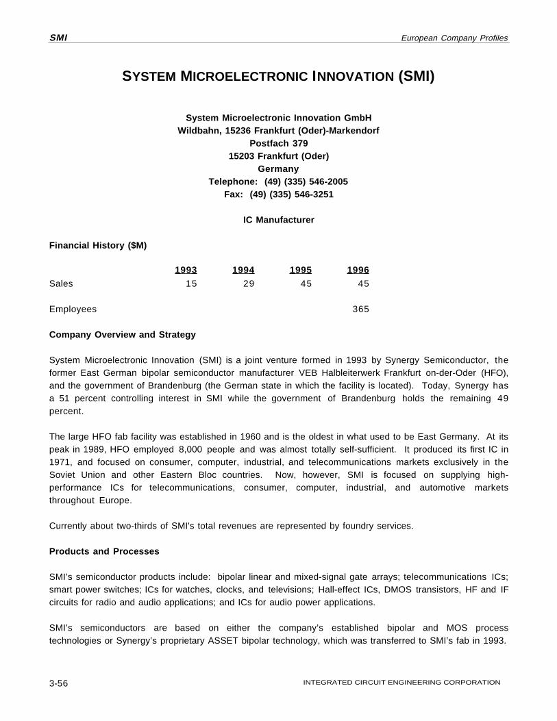
3-56
INTEGRATED CIRCUIT ENGINEERING CORPORATION
SMI European Company Profiles
SYSTEM MICROELECTRONIC INNOVATION (SMI)
System Microelectronic Innovation GmbHWildbahn, 15236 Frankfurt (Oder)-Markendorf
Postfach 37915203 Frankfurt (Oder)
GermanyTelephone: (49) (335) 546-2005
Fax: (49) (335) 546-3251
IC Manufacturer
Financial History ($M)
1993 1994 1995 1996
Sales 15 29 45 45
Employees 365
Company Overview and Strategy
System Microelectronic Innovation (SMI) is a joint venture formed in 1993 by Synergy Semiconductor, theformer East German bipolar semiconductor manufacturer VEB Halbleiterwerk Frankfurt on-der-Oder (HFO),and the government of Brandenburg (the German state in which the facility is located). Today, Synergy hasa 51 percent controlling interest in SMI while the government of Brandenburg holds the remaining 49percent.
The large HFO fab facility was established in 1960 and is the oldest in what used to be East Germany. At itspeak in 1989, HFO employed 8,000 people and was almost totally self-sufficient. It produced its first IC in1971, and focused on consumer, computer, industrial, and telecommunications markets exclusively in theSoviet Union and other Eastern Bloc countries. Now, however, SMI is focused on supplying high-performance ICs for telecommunications, consumer, computer, industrial, and automotive marketsthroughout Europe.
Currently about two-thirds of SMI's total revenues are represented by foundry services.
Products and Processes
SMI’s semiconductor products include: bipolar linear and mixed-signal gate arrays; telecommunications ICs;smart power switches; ICs for watches, clocks, and televisions; Hall-effect ICs, DMOS transistors, HF and IFcircuits for radio and audio applications; and ICs for audio power applications.
SMI’s semiconductors are based on either the company’s established bipolar and MOS processtechnologies or Synergy’s proprietary ASSET bipolar technology, which was transferred to SMI’s fab in 1993.

INTEGRATED CIRCUIT ENGINEERING CORPORATION 3-57
European Company Profiles SMI
Semiconductor Fabrication Facilities
SMI GmbHFrankfurt (Oder), GermanyCapacity (wafers/week): 2,400 (10,500 max.)Wafer size: 100mmProcesses: Bipolar, BiCMOS, MOSProducts: Logic, memory, and linear ICs; ASICsFeature sizes: ≥1.2µm
Key Agreements
• Synergy and SMI are codeveloping new products aimed at high-performance telecommunications andcomputational markets.
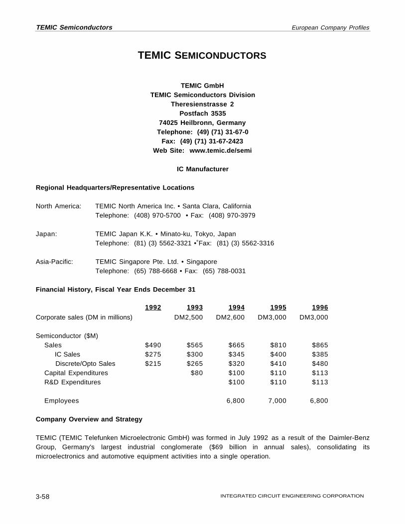
3-58
INTEGRATED CIRCUIT ENGINEERING CORPORATION
TEMIC Semiconductors European Company Profiles
TEMIC SEMICONDUCTORS
TEMIC GmbHTEMIC Semiconductors Division
Theresienstrasse 2Postfach 3535
74025 Heilbronn, GermanyTelephone: (49) (71) 31-67-0
Fax: (49) (71) 31-67-2423Web Site: www.temic.de/semi
IC Manufacturer
Regional Headquarters/Representative Locations
North America: TEMIC North America Inc. • Santa Clara, CaliforniaTelephone: (408) 970-5700 • Fax: (408) 970-3979
Japan: TEMIC Japan K.K. • Minato-ku, Tokyo, JapanTelephone: (81) (3) 5562-3321 • Fax: (81) (3) 5562-3316
Asia-Pacific: TEMIC Singapore Pte. Ltd. • SingaporeTelephone: (65) 788-6668 • Fax: (65) 788-0031
Financial History, Fiscal Year Ends December 31
1992 1993 1994 1995 1996
Corporate sales (DM in millions) DM2,500 DM2,600 DM3,000 DM3,000
Semiconductor ($M)Sales $490 $565 $665 $810 $865 IC Sales $275 $300 $345 $400 $385 Discrete/Opto Sales $215 $265 $320 $410 $480Capital Expenditures $80 $100 $110 $113R&D Expenditures $100 $110 $113
Employees 6,800 7,000 6,800
Company Overview and Strategy
TEMIC (TEMIC Telefunken Microelectronic GmbH) was formed in July 1992 as a result of the Daimler-BenzGroup, Germany's largest industrial conglomerate ($69 billion in annual sales), consolidating itsmicroelectronics and automotive equipment activities into a single operation.

INTEGRATED CIRCUIT ENGINEERING CORPORATION 3-59
European Company Profiles TEMIC Semiconductors
TEMIC is owned by Daimler-Benz and consists of three business units: Semiconductors, Microsystems(high-frequency components, electronic controls and sensor systems, power hybrids), and AutomotiveElectronics (systems and components for chassis control, comfort electronics, and vehicle safety). About 80percent of TEMIC's sales are made on the global market and the remaining 20 percent within the Daimler-Benz Group.
The TEMIC Semiconductors business unit combines the products, experience, and technologies ofTelefunken Semiconductors (Heilbronn, Germany), Siliconix* (Santa Clara, California), Matra MHS* (Nantes,France), and Dialog Semiconductor* (Swindon, United Kingdom), in addition to the design capabilities ofTEMIC Design Center for Integrated Circuits (Germany). Together, these companies represent Europe'sfourth largest semiconductor manufacturer, providing a wide variety of semiconductors to serve applicationsin digital, analog, mixed-signal, optical, and power circuitry.
Automotive21%
1996 Semiconductor Sales byEnd-Use Market
Computer15%
Industrial15%
AMS 6% Consumer
22%
Communications21%
Europe49%
1996 Semiconductor Sales by Geographic Region
North America21%
Asia Pacific22%
Japan8%
In mid-1996, TEMIC reorganized its Semiconductors business unit into two product divisions (DiscreteComponents and Integrated Circuits) and one worldwide sales division. The new arrangement is moremarket focused instead of company focused, which means that the names of the companies under TEMICSemiconductors will likely diminish in significance.
The Integrated Circuits division, headquartered in Heilbronn, consists of four product segments: Automotive(Heilbronn), Communications (Heilbronn), Controllers and Standard Products (Nantes), and ASICs (Swindon).The Discrete Components division, headquartered in Santa Clara, is also made up of four productsegments: Power MOSFETs (Santa Clara), Optoelectronics (Heilbronn), Diodes and Transistors(Vöcklabruck, Austria), and JFETs and LPDMOS Modules (Singapore).
Product areas of focus for TEMIC Semiconductors include RF and IR devices, automotive ICs with intelligentinterface and load drivers, embedded microcontrollers, mixed-signal ASICs for communications andbroadcast media applications, power ICs for disk drive motor control and power conversion applications,power MOSFETs, signal processing discretes, and optoelectronic components.
TEMIC Semiconductors is expanding its product offerings into areas such as DSPs, MCUs, and flashmemories through cooperation’s and licensing pacts with other semiconductor firms.
*Individual profiles of Siliconix, Matra MHS, and Dialog Semiconductor are included in this publication.

3-60
INTEGRATED CIRCUIT ENGINEERING CORPORATION
TEMIC Semiconductors European Company Profiles
Management
Frank Dieter Maier Chairman, President, and Chief Executive Officer, TEMIC GmbHHanspeter Eberhardt Senior Vice President, TEMIC SemiconductorsFrank Heinricht, Ph.D. General Manager, IC Division, TEMIC SemiconductorsRichard J. Kulle General Manager, Discretes Division, TEMIC Semiconductors, and
Chief Executive Officer, SiliconixMichel Thouvenin General Manager, Worldwide Sales, TEMIC Semiconductors
Products and Processes
TEMIC Semiconductors offers a broad range of products including digital, analog, and mixed-signal ASICsand ASSPs (for aerospace and defense, automotive, broadcast media, communications,computer/multimedia, and industrial applications), microcontrollers, high-performance SRAMs, power ICs,analog switches and multiplexers, discrete devices, and optoelectronic components. These devices arebased on a variety of processes including RF, CMOS, DMOS, bipolar, BiCMOS, BCDMOS(bipolar/CMOS/DMOS), GaAs, and silicon-germanium (SiGe). TEMIC also offers digital and mixed-signalCMOS and BiCMOS foundry services.
MOS MEMORY ANALOG
DRAM ✔ Amplifier
✔ SRAM ✔ Interface
Flash Memory ✔ Consumer/Automotive
EPROM Voltage Regulator/Reference
ROM ✔ Data Conversion
EEPROM Comparator
✔ Other (Including Non-Volatile RAM) ✔ Other (Includes Telecom)
MOS LOGIC DIGITAL BIPOLAR
General Purpose Logic Bipolar Memory
✔ Gate Array General Purpose Logic
✔ Standard Cell Gate Array/Standard Cell
✔ Field Programmable Logic Field Programmable Logic
✔ Other Special Purpose Logic Other Special Purpose Logic
MPU/MCU/MPR
MOS MICROCOMPONENT
MPU OTHER
✔ MCU ✔ Full Custom IC
MPR ✔ Discrete
✔ DSP ✔ Optoelectronic

INTEGRATED CIRCUIT ENGINEERING CORPORATION 3-61
European Company Profiles TEMIC Semiconductors
Telefunken Semiconductors' products include automotive control ICs, battery charge control ICs, IF/RFtransmission ICs, audio/video/telecom signal processing ICs, discrete devices, and optoelectroniccomponents. Technologies used to produce these devices include advanced bipolar, BiCMOS, GaAs,and SiGe processes.
Eurosil, a subsidiary of Telefunken Semiconductors, supplies low-power, low-voltage CMOS circuits forbattery operated applications such as watch and identification circuits.
Siliconix specializes in the design and manufacture of products for power management and motioncontrol. These devices include power MOSFETs, pulse width modulation (PWM) regulators andcontrollers, power ICs for motor and motion control, analog switches, and audio/video switching,buffering, and multiplexing ICs.
Matra MHS designs and manufactures high-performance specialty VLSI circuits using advanced digitalCMOS and BiCMOS technologies. Its products include very-low-power SRAMs (16K to 1M, 3V or 5V),high-speed SRAMs (16K to 256K, access times as low as 15ns), dual-port RAMs (8K to 128K), FIFOs,SPARClet™ 32-bit RISC embedded controllers, 4-bit MARC4 family of MCUs, 8-bit MCUs based on the80C51 and 80C251 architectures, gate array ASICs, embedded array ASICs, standard cell ASICs,Universal Logic Circuits (ULCs) for FPGA and PLD replacement, and full custom circuits. MHS alsoprovides ASSPs for communications, audio and video compression and conversion, automotivesystems, and aerospace applications.
Under a license agreement signed between TEMIC and Analog Devices in early 1997, Matramanufactures radiation-tolerant 32-bit floating-point DSPs for radiation-sensitive applications. The DSPis based on Analog Devices’ high-performance ADSP-21020 architecture and is built using a 0.6µmrad-hard CMOS process.
Dialog Semiconductor is a leading supplier of mixed-signal ASICs based on CMOS and BiCMOStechnologies for communications, consumer electronics, computers, industrial equipment, medicalinstrumentation, and automotive systems.
Discretes42%
1996 Semiconductor Sales byProduct Type
Opto13%
CMOS ICs28%
Bipolar ICs17%
MCUs andDigital ICs
41%
1996 IC Sales by Product Type
Power ICs9%
Automotive ICs26%
Communications ICs18%
Mixed-Signal ASICs6%

3-62
INTEGRATED CIRCUIT ENGINEERING CORPORATION
TEMIC Semiconductors European Company Profiles
Semiconductor Fabrication Facilities
TEMIC, Telefunken Semiconductors TEMIC, Telefunken SemiconductorsTheresienstrasse 2 Theresienstrasse 274072 Heilbronn, Germany 74072 Heilbronn, GermanyCapacity (wafers/week): 15,000 Capacity (wafers/week): 750Wafer sizes: 100mm, 150mm Wafer size: 3inProcesses: Bipolar, CMOS, BiCMOS, SiGe Process: GaAsProducts: ASICs, ASSPs, MCUs, logic ICs, Products: Optoelectronics linear ICs, custom ICs, discretes, opto Feature size: 1.0µmFeature sizes: 0.8µm-3.0µm
TEMIC TEMIC, SiliconixTelefunkenstrasse 5 Itzehoe, Germany4840 Vöcklabruck, Austria Cleanroom size: 44,000 square feet (Class 1)Wafer size: 100mm Wafer sizes: 150mm, 200mmProcess: Bipolar Processes: PowerMOS, BiCMOSProducts: Discretes Products: Discretes
TEMIC, Matra MHS TEMIC, SiliconixLa Chanterie-Route de Gachet 2201 Laurelwood RoadCP 3008 P.O. Box 5495144087 Nantes Cedex 03 Santa Clara, California 95056-9951France Telephone: (408) 988-8000Telephone: (33) (2) 40-18-18-18 Capacity (wafers/week): 3,500Cleanroom size: 30,000 square feet (Class 1) Wafer sizes: 100mm, 150mmCapacity (wafers/week): 3,500 Processes: CMOS, DMOS, BCDMOS, BiCMOSWafer size: 150mm Products: Discretes, Power ICs, analog ICsProcesses: CMOS, BiCMOS, rad-hard CMOS Feature sizes: 0.8µm-3.0µmProducts: ASICs, ASSPs, MCUs, MPUs, SRAMs, DSPsFeature sizes: 0.5µm, 0.6µm, 0.8µm, 0.85µm (0.35µm process under development)

INTEGRATED CIRCUIT ENGINEERING CORPORATION 3-63
European Company Profiles TEMIC Semiconductors
Key Agreements
• In June 1996, TEMIC and the Fraunhofer-Institut für Siliziumtechnologie (ISIT) in Itzehoe, Germany,established a close relationship. TEMIC is using part of ISIT’s cleanroom and equipment for massproduction of powerMOS discretes. In 2Q97, TEMIC began processing 150mm wafers in the fab, butplans to quickly migrate to 200mm wafers, making it one of the first companies to use the large wafers fordiscrete devices. TEMIC also agreed to jointly develop new technologies with ISIT, who is engaged in thedevelopment of 0.5µm and smaller geometry CMOS process technologies.
• See also individual profiles of Siliconix, Matra MHS, and Dialog Semiconductor.
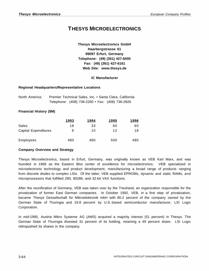
3-64
INTEGRATED CIRCUIT ENGINEERING CORPORATION
Thesys Microelectronics European Company Profiles
THESYS MICROELECTRONICS
Thesys Microelectronics GmbHHaarbergstrasse 61
99097 Erfurt, GermanyTelephone: (49) (361) 427-6000
Fax: (49) (361) 427-6161Web Site: www.thesys.de
IC Manufacturer
Regional Headquarters/Representative Locations
North America: Premier Technical Sales, Inc. • Santa Clara, CaliforniaTelephone: (408) 736-2260 • Fax: (408) 736-2826
Financial History ($M)
1993 1994 1995 1996
Sales 18 33 60 60Capital Expenditures 9 10 12 18
Employees 480 480 500 480
Company Overview and Strategy
Thesys Microelectronics, based in Erfurt, Germany, was originally known as VEB Karl Marx, and wasfounded in 1968 as the Eastern Bloc center of excellence for microelectronics. VEB specialized inmicroelectronic technology and product development, manufacturing a broad range of products rangingfrom discrete diodes to complex LSIs. Of the latter, VEB supplied EPROMs, dynamic and static RAMs, andmicroprocessors that fulfilled Z80, 80286, and 32-bit VAX functions.
After the reunification of Germany, VEB was taken over by the Treuhand, an organization responsible for theprivatization of former East German companies. In October 1992, VEB, in a first step of privatization,became Thesys Gessellschaft für Mikroelektronik mbH with 80.2 percent of the company owned by theGerman State of Thuringia and 19.8 percent by U.S.-based semiconductor manufacturer, LSI LogicCorporation.
In mid-1995, Austria Mikro Systeme AG (AMS) acquired a majority interest (51 percent) in Thesys. TheGerman State of Thuringia divested 31 percent of its holding, retaining a 49 percent share. LSI Logicrelinquished its shares in the company.

INTEGRATED CIRCUIT ENGINEERING CORPORATION 3-65
European Company Profiles Thesys Microelectronics
Through the ownership by AMS, Thesys receives free process, design, and product/technology transfersfrom AMS. In addition, the design and production capabilities of Thesys’ fab facility is being upgraded andexpanded.
Thesys specializes in application-specific semiconductors and offers capabilities ranging from FPGA to ASICconversions, mixed-signal ASICs and ASSPs to foundry services. Thesys’ mixed-signal technologies provideunique solutions for traditional telecommunication, automotive, and industrial applications, as well as forevolving wireless communication and multimedia markets.
Management
Hans-Jürgen Straub President and Chief Financial OfficerKonrad Herre Vice President, Production and Development
Products and Processes
Thesys' IC products include analog, digital, and mixed-signal CMOS and BiCMOS ASICs (gate arrays andstandard cells) and ASSPs, high-frequency BiCMOS devices, and full-custom ICs. Its ASICs are availablewith up to 150,000 available gates and up to 488 pins. Thesys also provides image processing systemsupport and design, as well as foundry services.
Thesys has design centers located in Düsseldorf, Frankfurt, Munich, and Stuttgart.
Semiconductor Fabrication Facilities
To supplement its own manufacturing capacity, Thesys has established foundry agreements with Zilog, LSILogic, and UMC.
Thesys Microelectronics GmbHHaarbergstrasse 6199097 Erfurt, GermanyCleanroom size: 10,670 square feet (Class 1)Capacity (wafers/week): 2,100Wafer size: 150mmProcesses: CMOS, BiCMOSProducts: Analog, digital, and mixed-signal ASICs; ASSPs; foundry servicesFeature sizes: 0.6µm-1.5µm
Key Agreements
• Thesys and Austria Mikro Systeme (AMS) have a product development agreement. The agreementcovers free process, design, and product technology transfers from AMS to Thesys, while BiCMOS andCMOS expertise at both companies is shared. As part of the agreement, AMS and Thesys aredeveloping a new mixed-signal 0.6µm CMOS process which will be fully qualified for production in 1997.AMS has a 51 percent controlling interest in Thesys.

3-66
INTEGRATED CIRCUIT ENGINEERING CORPORATION
Thesys Microelectronics European Company Profiles
• Thesys and IMEC, Belgium’s Research Institute for Microelectronics, announced a license agreement thatallows Thesys to use IMEC’s flash memory technology. IMEC developed the solution for 0.7µmtechnology, which provides an ideal starting point for industrial implementation with Thesys’ 0.8µmprocess. Consideration is already been given for further scaling of the HIMOS technology to the 0.6µmplatform currently under development at Thesys.
• Thesys concluded an agreement with United Microelectronics Corporation (UMC) of Taiwan in early 1994that brought UMC’s 0.8µm process technology to Thesys’ manufacturing facility in Erfurt.
• Thesys formed a strategic partnership and technology licensing agreement with Aspec Technology, SantaClara, California, in early 1994. The deal allows Thesys to design and manufacture 0.8µm ASIC gatearray and embedded array products using Aspec's Portfolio family of HDA design tools.

INTEGRATED CIRCUIT ENGINEERING CORPORATION 3-67
European Company Profiles Thomson-CSF Semiconducteurs Specifiques
THOMSON-CSF SEMICONDUCTEURS SPECIFIQUES (TCS)
Thomson-CSF Semiconducteurs SpecifiquesRoute Départmentale 128, BP 46
91401 Orsay CedexFrance
Telephone: (33) (1) 69-33-00-00Fax: (33) (1) 69-33-03-21
Web Site: www.tcs.thomson-csf.com
IC Manufacturer
Regional Headquarters/Representative Locations
North America: Thomson Components and Tubes Corporation, TCS Division • Totowa, New JerseyTelephone: (201) 812-9000 • Fax: (201) 812-9050
Asia: Thomson Tubes Electroniques • New Delhi, IndiaTelephone: (91) (11) 644-78-83 • Fax: (91) (11) 648-26-84
Company Overview and Strategy
Thomson-CSF Semiconducteurs Specifiques (TCS) is a subsidiary of Thomson-CSF, the professionalelectronics wing of France’s Thomson SA. Thomson-CSF develops and supports advanced electronicequipment and systems for security, information, and communications applications in military and civilmarkets. As a side note, Thomson-CSF owns 20 percent of SGS-Thomson Microelectronics.
Since the mid-1970’s TCS has been designing, manufacturing, and marketing high-reliability (hi-rel)semiconductors for military, aerospace, and professional electronics applications. Its semiconductorproducts include ASICs, microprocessors and controllers, non-volatile memories, linear devices, and imagesensors. Through its long-term cooperation and license partnerships with major semiconductor supplierssuch as Motorola and SGS-Thomson Microelectronics, TCS is able to offer hi-rel versions of leading edgecommercial technologies and products. In addition, to meet the long lifecycle requirements of hi-rel systems,the company has implemented a specific strategy to insure that its devices are available for periods inexcess of 25 years.
Products and Processes
TCS has three hi-rel semiconductor product lines: standard products, including microcomponents, non-volatile memories, and linear ICs; ASIC products from linear to digital and mixed-signal; and image sensors,including CCDs and infrared sensors.
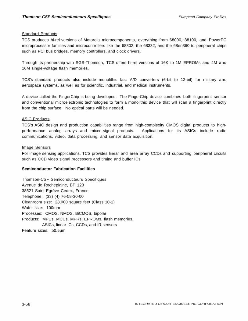
3-68
INTEGRATED CIRCUIT ENGINEERING CORPORATION
Thomson-CSF Semiconducteurs Specifiques European Company Profiles
Standard Products
TCS produces hi-rel versions of Motorola microcomponents, everything from 68000, 88100, and PowerPCmicroprocessor families and microcontrollers like the 68302, the 68332, and the 68en360 to peripheral chipssuch as PCI bus bridges, memory controllers, and clock drivers.
Through its partnership with SGS-Thomson, TCS offers hi-rel versions of 16K to 1M EPROMs and 4M and16M single-voltage flash memories.
TCS’s standard products also include monolithic fast A/D converters (6-bit to 12-bit) for military andaerospace systems, as well as for scientific, industrial, and medical instruments.
A device called the FingerChip is being developed. The FingerChip device combines both fingerprint sensorand conventional microelectronic technologies to form a monolithic device that will scan a fingerprint directlyfrom the chip surface. No optical parts will be needed.
ASIC Products
TCS’s ASIC design and production capabilities range from high-complexity CMOS digital products to high-performance analog arrays and mixed-signal products. Applications for its ASICs include radiocommunications, video, data processing, and sensor data acquisition.
Image Sensors
For image sensing applications, TCS provides linear and area array CCDs and supporting peripheral circuitssuch as CCD video signal processors and timing and buffer ICs.
Semiconductor Fabrication Facilities
Thomson-CSF Semiconducteurs SpecifiquesAvenue de Rocheplaine, BP 12338521 Saint-Egrève Cedex, FranceTelephone: (33) (4) 76-58-30-00Cleanroom size: 28,000 square feet (Class 10-1)Wafer size: 100mmProcesses: CMOS, NMOS, BiCMOS, bipolarProducts: MPUs, MCUs, MPRs, EPROMs, flash memories, ASICs, linear ICs, CCDs, and IR sensorsFeature sizes: ≥0.5µm

INTEGRATED CIRCUIT ENGINEERING CORPORATION 3-69
European Company Profiles VTT Electronics
VTT ELECTRONICS
VTT ElectronicsTekniikantie 17
FIN-02150 Espoo, FinlandTelephone: (358) (9) 456-1
Fax: (358) (9) 456-7012Web Site: www.ele.vtt.fi
IC Manufacturer
Company Overview and Strategy
VTT (Valtion Teknillinen Tutkimuskeskus) is a contract research and development laboratory for appliedtechnical research. Two thirds of its research is contract-based and one third is self-initiated. Total staff is2,700. VTT Electronics is one of the nine VTT research institutes, with a staff of 250. Research anddevelopment covers IC materials, processing and design, electronics hardware, measurement systems, andembedded software. VTT’s budget for microelectronics research in 1996 was approximately $10 million.
VTT’s integrated circuit activities include process integration, process module development, circuit design,modeling, and test. The main emphasis is on mixed analog/digital technology for telecom, instrumentationand interface circuits, such as RFICs, sensor interfaces, and power circuits.
Other activities in silicon include crystal growth and epitaxy, silicon room-temperature radiation detectors, andsilicon micro-mechanical and micro-optical sensors.
Management
Tapio Wiik, Ph.D. Manager, Process TechnologyMarkku Aberg, Ph.D. Manager, Design and Modeling
Products and Processes
VTT Electronics uses various process technologies including mixed-signal 0.8µm analog/digital CMOS(custom processes available), 0.8µm RF BiCMOS (24GHz, capacitors, resistors), and 0.6µm RF BiCMOS(30GHz, under development, includes inductors). Its products include RFICs, power ICs, silicon radiationdetectors (3.0µm MOS), and silicon microsensors (bulk and surface).
3-70
INTEGRATED CIRCUIT ENGINEERING CORPORATION
VTT Electronics European Company Profiles
Semiconductor Fabrication Facilities
VTT Electronics moved into a new Microelectronics Center in early 1997.
VTT ElectronicsTekniikantie 17FIN-02150 Espoo, FinlandCleanroom size: 11,000 square-feet (Class 10)Wafer size: 100mmProcesses: CMOS, BiCMOSFeature size: 0.8µm

INTEGRATED CIRCUIT ENGINEERING CORPORATION 3-71
European Company Profiles ZMD
ZENTRUM MIKROELEKTRONIK DRESDEN (ZMD)
Zentrum Mikroelektronik Dresden GmbH (ZMD)Grenzstrasse 28, Postfach 34
01109 Dresden, GermanyTelephone: (49) (351) 8822-0
Fax: (49) (351) 8822-600Web Site: www.zmd-gmbh.de
IC Manufacturer
Regional Headquarters/Representative Locations
North America: ZMD America Inc. • Santa Clara, CaliforniaTelephone: (408) 562-6072 • Fax: (408) 562-6073 • Web Site: www.zmda.com
Financial History ($M)
1994 1995 1996
Sales* 8 24 41Capital Expenditures 27 23 15
Employees 560 550 490
*IC Sales only. SIMM-business separated from ZMD in 1996.
Company Overview and Strategy
Zentrum Mikroelektronik Dresden (ZMD) develops, manufactures, and supplies integrated circuits andmultichip modules, focusing mainly on application-specific integrated circuits (ASICs) and application-specificmemory products.
ZMD was founded in 1961 as a leading research and development center in Eastern Europe. ZMD was thefirst East European company to build a 1M DRAM and to introduce ASIC technology. With more than 30years of experience in the field of microelectronics, ZMD was re-founded as a private company in 1993 as aresult of the reunification of Germany.

3-72
INTEGRATED CIRCUIT ENGINEERING CORPORATION
ZMD European Company Profiles
The company’s core business is silicon manufacturing. ZMD’s three business units are: Foundry, MemoryICs, and Logic ICs. The Foundry business designs, manufactures, tests, and packages digital and mixed-signal ICs for semiconductor manufacturers, fabless IC suppliers, and systems and hardware manufacturers.Silicon foundry customers include Siemens, Philips, and TEMIC. Memory products from ZMD comprisethree sectors: standard SRAM, application-specific SRAM, and non-volatile memories (nvSRAMs). TheLogic IC business specializes in gate array and cell-based ASICs, DSPs, and identification systemsparticularly for automotive and communications applications. ZMD also provides its FPGA Fast PrototypingService and its FPGA-to-Gate Array Conversion Service to complete its semiconductor offerings.
Management
Heinz W. Hagmeister ChairmanKurt Garbrecht, Ph.D. Chief Executive Officer
Products and Processes
ZMD's product offerings include:ASICs
Analog/digital cell-based ICs (up to 500,000 transistors)Gate arrays (up to 100,000 transistors)
ASSPsTelecommunication ICsIndustrial communication ICsAutomotive electronics ICsMCUs
MemoryStandard SRAMsApplication-specific SRAMsNon-volatile SRAMs
PCMCIA Cards
ZMD develops and manufactures digital and mixed-signal ASIC products for customers in many sectors ofthe electronics industry. The mainstream ASIC families, based on 0.8µm SPDM CMOS technology, are theU2400 Cell Array Series and the U5600 Gate Array Series. Advanced features of the 0.8µm CMOS processare under development. In 1997, an EEPROM option, a second polysilicon layer option for resistors andcapacitors, a fuse option, and a high voltage transistor option (up to 40V) will be available. Also in 1997, alow voltage 0.8µm CMOS process operating on supply voltages down to 1.2V with options for EEPROM andanalog features for single-battery applications will be available.
In addition, ZMD offers 2.0µm and 1.2µm BiCMOS processes with high voltage transistors (up to 40V).Additional analog options make the BiCMOS processes also suitable for analog and mixed-signal design.
All ZMD technologies used for ASIC products are also offered for silicon foundry services. Additional servicesare provided for special customers like Siemens, Philips, or TEMIC, where their own technology is provided.

INTEGRATED CIRCUIT ENGINEERING CORPORATION 3-73
European Company Profiles ZMD
ZMD’s memory products are used in a variety of applications, but are well suited to industrial,communication, and automotive applications. Standard SRAMs up to 64K and application-specific SRAMs(specializing in fast automotive types up to 256K) are the platform of ZMD’s memory business. ZMD uses itsSRAM processes as technology drivers and a manufacturing base.
The current strategy of ZMD’s memory products business is focused on nvSRAM technology. The nvSRAMnot only provides the advantages of fast SRAMs but also those of EPROMs. Development of nvSRAMoccurs jointly with Colorado Springs, Colorado-based Simtek. ZMD’s new 64K and 256K nvSRAM productfamilies are available with access times of 25ns, 35ns, and 45ns. ZMD expects to introduce new nvSRAMsproducts with densities ranging from 4K to 1M during 1997.
Semiconductor Fabrication Facilities
Zentrum Mikroelektronik Dresden GmbHGrenzstrasse 28Postfach 3401109 Dresden, GermanyCleanroom size: 16,000 square feet, Class 10 (locally Class 1)Capacity (wafers/week): 2,000Wafer size: 125mmProcesses: CMOS, BiCMOSProducts: ASICs; memory, microcomponent, and telecom ICs; DSPs; foundry servicesFeature sizes: 0.8µm-2.0µm CMOS
0.8µm SNOS-CMOS0.8µm-1.2µm Analog CMOS1.2µm, 2.0µm BiCMOS
Key Agreements
• ZMD signed an agreement with Simtek in mid-1994 to jointly develop 0.8µm nvSRAM products.

3-74
INTEGRATED CIRCUIT ENGINEERING CORPORATION
European Company Profiles