ese 570: digital integrated circuits and vlsi fundamentalsese570/spring2016/handouts/lec1.pdf ·...
TRANSCRIPT
ESE 570: Digital Integrated Circuits and VLSI Fundamentals
Lec 1: January 14, 2016 Introduction and Overview
Penn ESE 570 Spring 2016 - Khanna
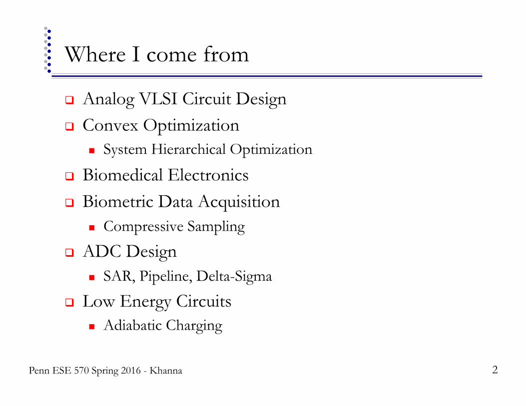
Where I come from
! Analog VLSI Circuit Design ! Convex Optimization
" System Hierarchical Optimization
! Biomedical Electronics ! Biometric Data Acquisition
" Compressive Sampling
! ADC Design " SAR, Pipeline, Delta-Sigma
! Low Energy Circuits " Adiabatic Charging
2 Penn ESE 570 Spring 2016 - Khanna
IC
< 5mm
< 2mm
Bio-friendly package
Bare die Ultra-
capacitor
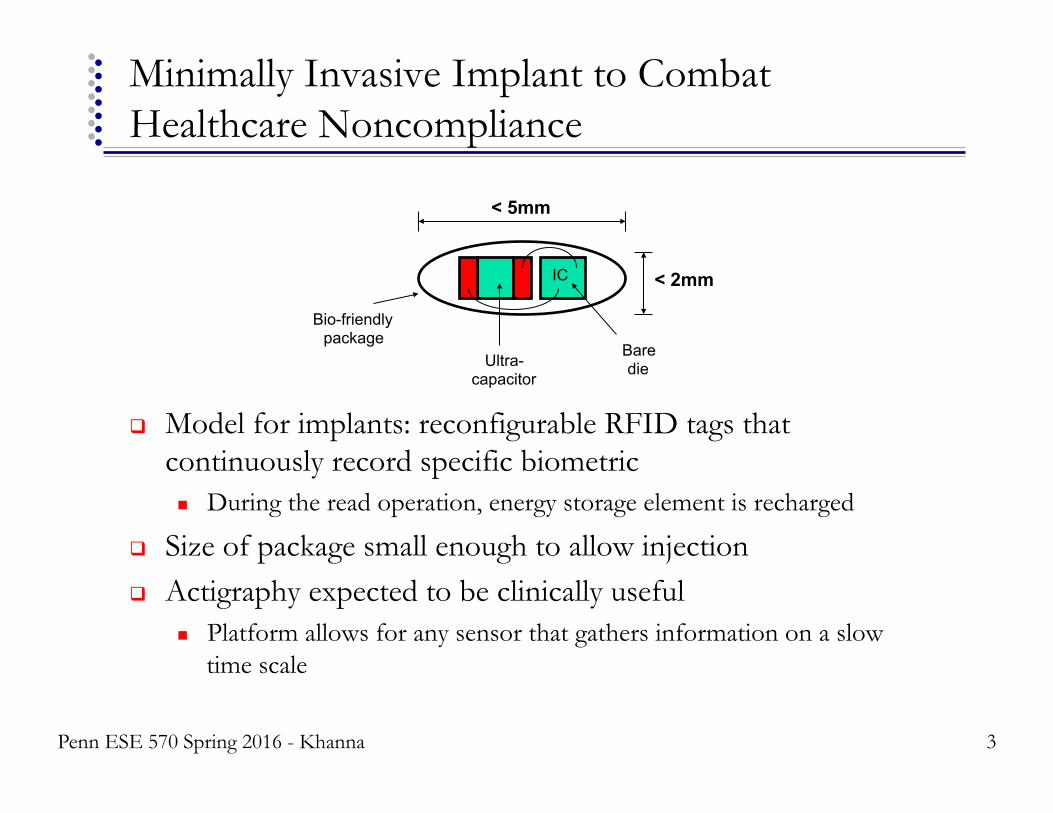
Minimally Invasive Implant to Combat Healthcare Noncompliance
! Model for implants: reconfigurable RFID tags that continuously record specific biometric " During the read operation, energy storage element is recharged
! Size of package small enough to allow injection ! Actigraphy expected to be clinically useful
" Platform allows for any sensor that gathers information on a slow time scale
3 Penn ESE 570 Spring 2016 - Khanna

MicroImplant: An Electronic Platform for Minimally Invasive Sensory Monitors
4 Penn ESE 570 Spring 2016 - Khanna

Getting to Know You
! Graduate? ! Undergraduate? ! ESE 419/572?
! What do you hope to get out of this class?
5 Penn ESE 570 Spring 2016 - Khanna
Lecture Outline
! Course Topics Overview ! Learning Objectives ! Course Structure ! Course Policies ! Course Content ! Industry Trends ! Design Example
6 Penn ESE370 Fall2015 – Khanna
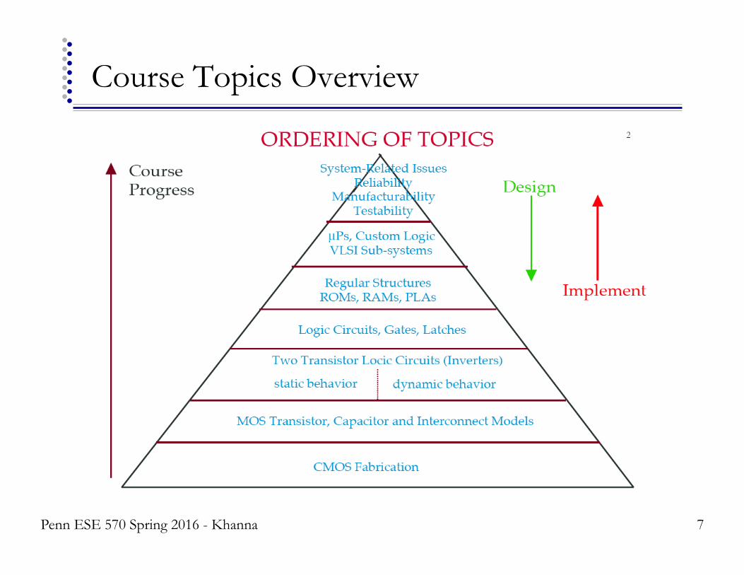
Course Topics Overview
7 Penn ESE 570 Spring 2016 - Khanna
Learning Objectives
! Apply principles of hierarchical digital CMOS VLSI, from the transistor up to the system level, to the understanding of CMOS circuits and systems that are suitable for CMOS fabrication.
! Apply the models for state-of-the-art VLSI components, fabrication steps, hierarchical design flow and semiconductor business economics to judge the manufacturability of a design and estimate its manufacturing costs.
! Design simulated experiments using Cadence to verify the integrity of a CMOS circuit and its layout.
! Design digital circuits that are manufacturable in CMOS. ! Apply the Cadence VLSI CAD tool suite layout digital circuits for CMOS
fabrication and verify said circuits with layout parasitic elements. ! Apply course knowledge and the Cadence VLSI CAD tools in a team based
capstone design project that involves much the same design flow they would encounter in a semiconductor design industrial setting. Capstone project is presented in a formal report due at the end of the semester.
8 Penn ESE 570 Spring 2016 - Khanna
Learning Objectives
! In other words…
! Design in CADENCE*
*All the way to manufacturability
9 Penn ESE 570 Spring 2016 - Khanna
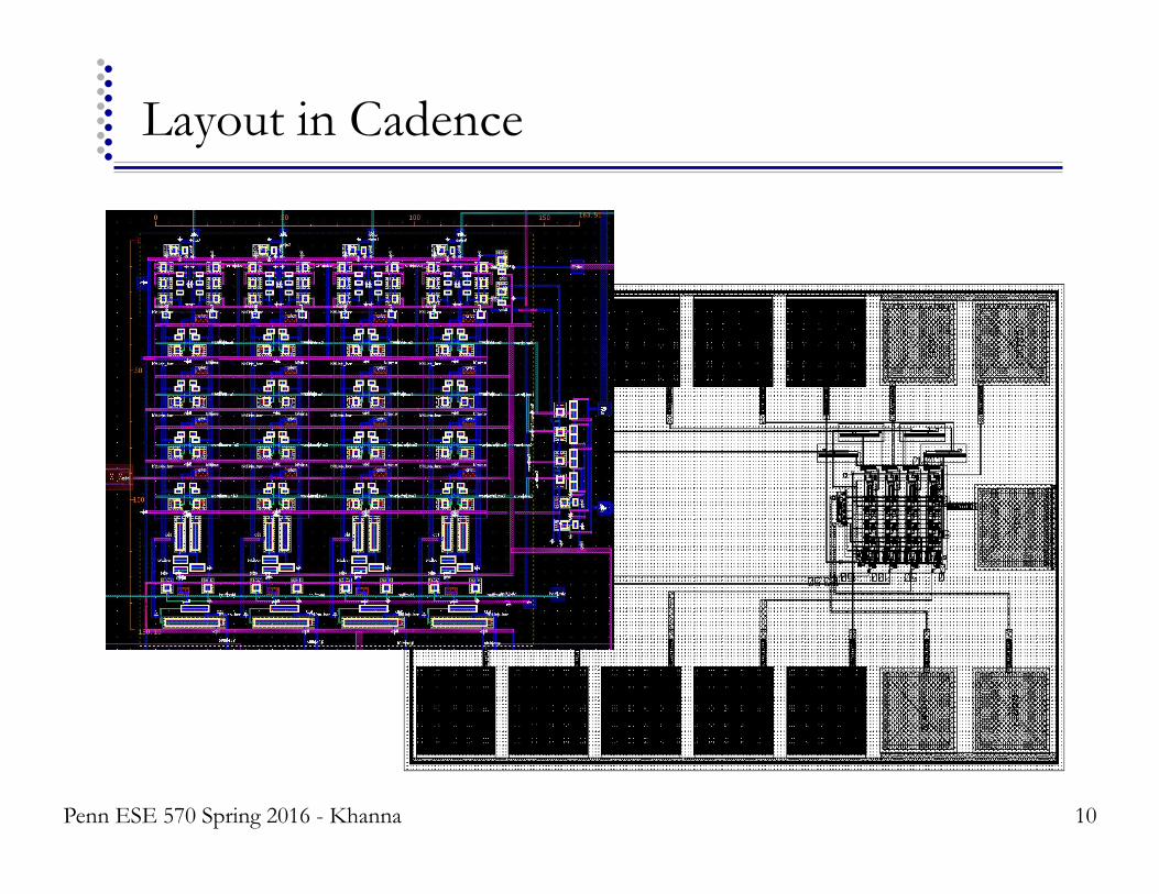
Layout in Cadence
10 Penn ESE 570 Spring 2016 - Khanna
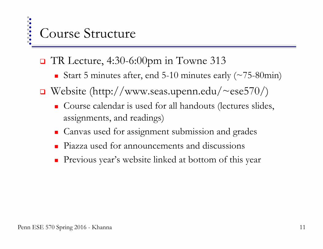
Course Structure
! TR Lecture, 4:30-6:00pm in Towne 313 " Start 5 minutes after, end 5-10 minutes early (~75-80min)
! Website (http://www.seas.upenn.edu/~ese570/) " Course calendar is used for all handouts (lectures slides,
assignments, and readings) " Canvas used for assignment submission and grades " Piazza used for announcements and discussions " Previous year’s website linked at bottom of this year
11 Penn ESE 570 Spring 2016 - Khanna
Course Structure
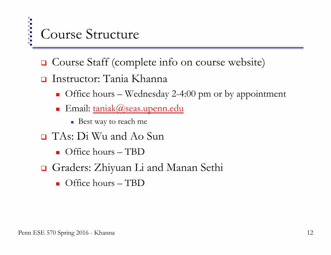
! Course Staff (complete info on course website) ! Instructor: Tania Khanna
" Office hours – Wednesday 2-4:00 pm or by appointment " Email: [email protected]
" Best way to reach me
! TAs: Di Wu and Ao Sun " Office hours – TBD
! Graders: Zhiyuan Li and Manan Sethi " Office hours – TBD
12 Penn ESE 570 Spring 2016 - Khanna
Course Structure
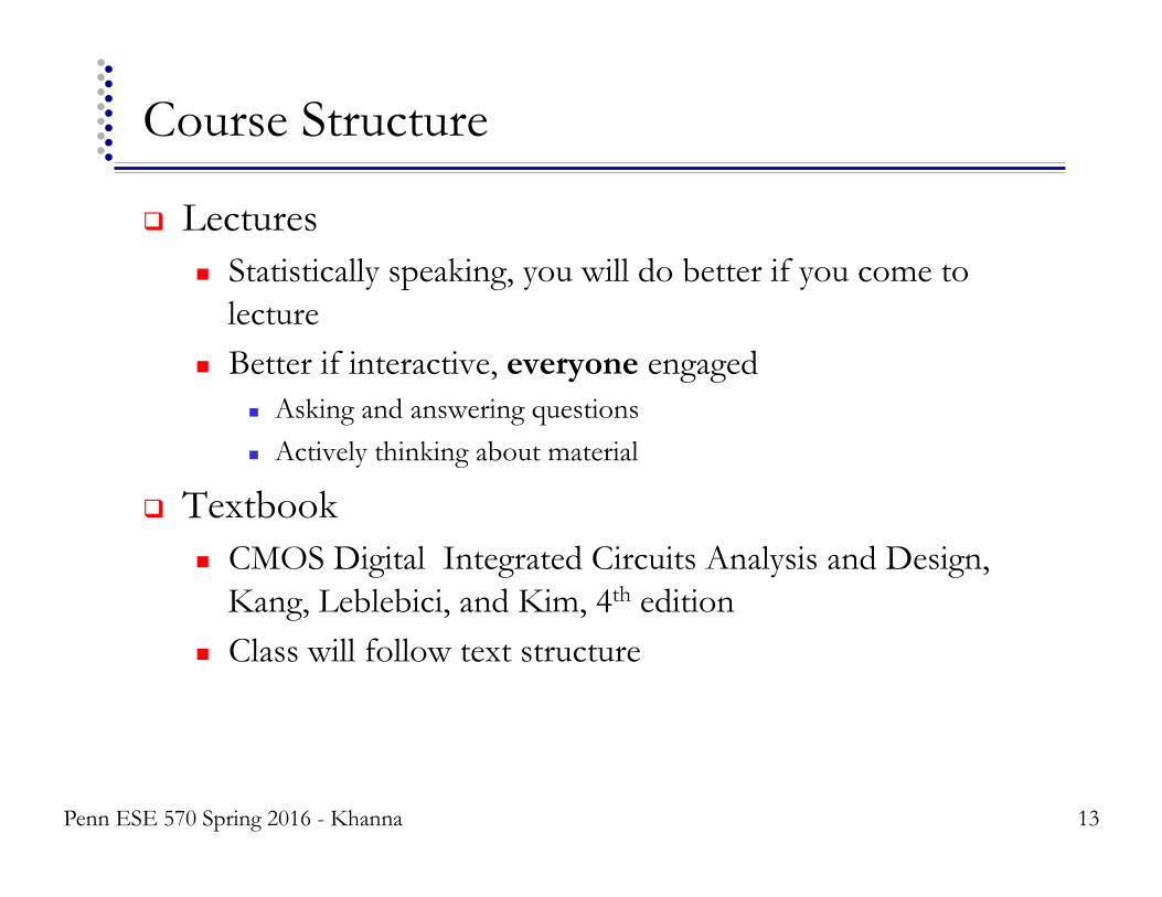
! Lectures " Statistically speaking, you will do better if you come to
lecture " Better if interactive, everyone engaged
" Asking and answering questions " Actively thinking about material
! Textbook " CMOS Digital Integrated Circuits Analysis and Design,
Kang, Leblebici, and Kim, 4th edition " Class will follow text structure
13 Penn ESE 570 Spring 2016 - Khanna
Course Structure
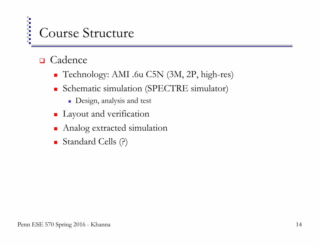
! Cadence " Technology: AMI .6u C5N (3M, 2P, high-res) " Schematic simulation (SPECTRE simulator)
" Design, analysis and test
" Layout and verification " Analog extracted simulation " Standard Cells (?)
14 Penn ESE 570 Spring 2016 - Khanna
Course Structure - Assignments/Exams
! Homework – 1-2 week(s) long (8 total) [25%] " Due Thursdays at start of class (4:30pm) " HW 1 out already
! Project – two+ weeks long (2 total) [30%] " Design oriented " Project proposed with inspiration list
" See previous course website for project topic samples
! Midterm exam [20%] ! Final exam [25%]
15 Penn ESE370 Fall2015 – Khanna
Course Policies
See web page for full details ! Turn homework in Canvas or in class before lecture
starts " Anything handwritten/drawn must be clearly legible " Submit CAD generated figures, graphs, results when
specified " NO LATE HOMEWORKS!
! Individual work (except project) " CAD drawings, simulations, analysis, writeups " May discuss strategies, but acknowledge help
16 Penn ESE370 Fall2015 – Khanna
Course Content
! Introduction ! Fabrication ! MOS Transistor Theory and
Models ! MOS Models and IV
characteristics ! Inverters: Static Characteristics
and Performance ! Inverters: Dynamic
Characteristics and Performance ! Combinational Logic Types
(CMOS, Ratioed, Pass) and Performance
! Sequential Logic ! Dynamic Logic ! VLSI design and Scaling ! Memory Design ! I/O Circuits and Inductive
Noise ! CLK Generation ! Robust VLSI Design for
Variation
17 Penn ESE 570 Spring 2016 - Khanna

Industry Trends
Penn ESE 570 Spring 2016 - Khanna 18
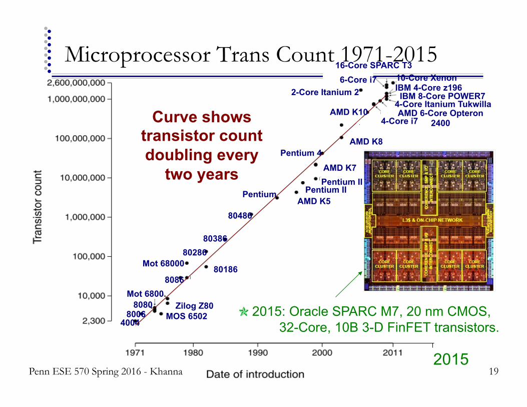
Microprocessor Trans Count 1971-2015
19 Kenneth R. Laker, University of Pennsylvania, updated 20Jan15
Curve shows transistor count doubling every
two years Pentium
4004 8006
8080 Mot 6800
8086
Mot 68000 80286
80386
80486
MOS 6502 Zilog Z80
80186
AMD K5 Pentium II
Pentium III AMD K7
Pentium 4 AMD K8
AMD K10 AMD 6-Core Opteron 2400 4-Core i7
2-Core Itanium 2 6-Core i7 6-Core i7 16-Core SPARC T3
10-Core Xenon IBM 4-Core z196 IBM 8-Core POWER7
4-Core Itanium Tukwilla
2015: Oracle SPARC M7, 20 nm CMOS, 32-Core, 10B 3-D FinFET transistors.
2015 Penn ESE 570 Spring 2016 - Khanna
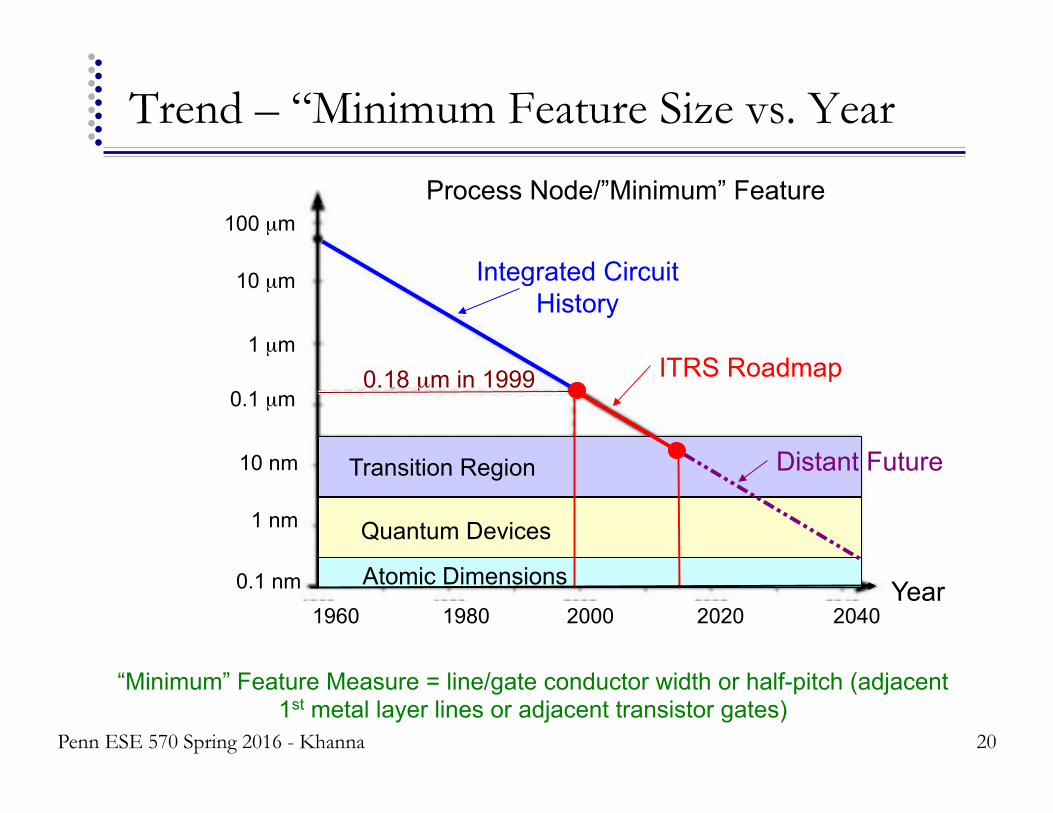
Trend – “Minimum Feature Size vs. Year
20
Process Node/”Minimum” Feature
Year 1960 1980 2000 2020 2040
100 µm
10 µm
1 µm
0.1 µm
10 nm
1 nm
0.1 nm
Integrated Circuit History
0.18 µm in 1999
Distant Future
ITRS Roadmap
Transition Region
Quantum Devices
Atomic Dimensions
“Minimum” Feature Measure = line/gate conductor width or half-pitch (adjacent 1st metal layer lines or adjacent transistor gates)
Penn ESE 570 Spring 2016 - Khanna
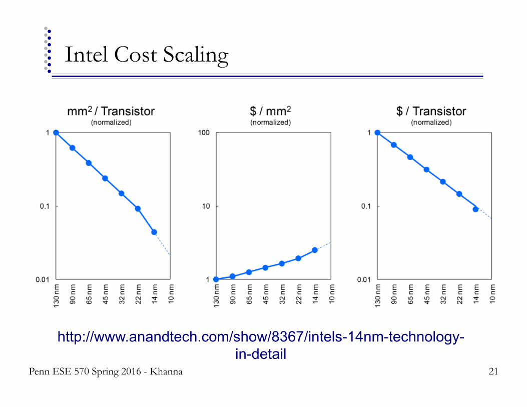
Intel Cost Scaling
21
http://www.anandtech.com/show/8367/intels-14nm-technology-in-detail
Penn ESE 570 Spring 2016 - Khanna
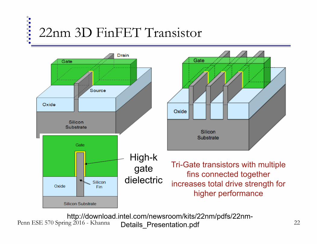
22nm 3D FinFET Transistor
22
Tri-Gate transistors with multiple fins connected together
increases total drive strength for higher performance
http://download.intel.com/newsroom/kits/22nm/pdfs/22nm-Details_Presentation.pdf
High-k gate
dielectric
Penn ESE 570 Spring 2016 - Khanna
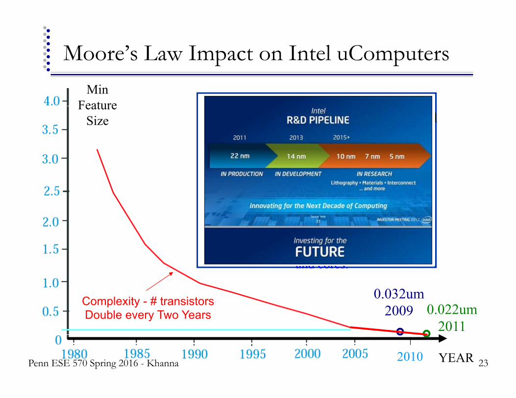
Moore’s Law Impact on Intel uComputers
23 2010 YEAR
Serial data links operating at 10 Gbits/sec.
Increased reuse of logic IP, i.e. designs and cores.
2BT µP (Intel Itanium Tukwila) 4-Core chip (65 nm) introduced Q1 2010.
3BT mP (Intel Itanium Poulson) 8-Core chip (32 nm) to be introduced 2012.
Introduces 22 nm Tri-gate Transistor Tech.
Complexity - # transistors Double every Two Years 0.022um
2011
0.032um 2009
Min Feature
Size
Penn ESE 570 Spring 2016 - Khanna
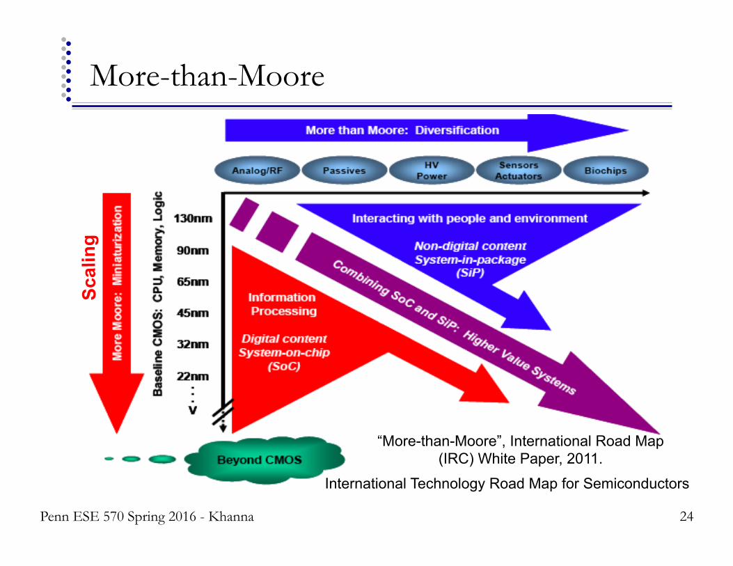
More-than-Moore
24
“More-than-Moore”, International Road Map (IRC) White Paper, 2011.
International Technology Road Map for Semiconductors
Scal
ing
Penn ESE 570 Spring 2016 - Khanna
More Moore # Scaling
! Geometrical Scaling " continued shrinking of horizontal and vertical physical
feature sizes
! Equivalent Scaling " 3-dimensional device structure improvements and new
materials that affect the electrical performance of the chip even if no geometrical scaling
! Design Equivalent Scaling " design technologies that enable high performance, low
power, high reliability, low cost, and high design productivity even if neither geometrical nor equivalent scaling can be used
25 Penn ESE 570 Spring 2016 - Khanna
More Moore # Scaling
! Examples: " Design-for-variability " Low power design (sleep modes, clock gating, multi-
Vdd, etc.) " Multi-core SOC architectures
26 Penn ESE 570 Spring 2016 - Khanna
More than Moore # Functional Diversification
! Interacting with the outside world " Electromagnetic/Optical
" Radio-frequency domain up to the THz range " Optical domain from the infrared to the near ultraviolet " Hard radiation (EUV, X-ray, γ-ray)
" Mechanical parameters (sensors/actuators) " MEMS/NEMS position, speed, acceleration, rotation,
pressure, stress, etc.
" Chemical composition (sensors/actuators) " Biological parameters (sensors/actuators)
! Power/Energy " Integration of renewable sources, Energy storage, Smart
metering, Efficient consumption 27 Penn ESE 570 Spring 2016 - Khanna
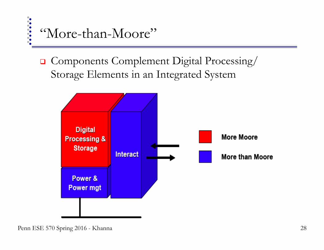
“More-than-Moore”
! Components Complement Digital Processing/Storage Elements in an Integrated System
28 Penn ESE 570 Spring 2016 - Khanna
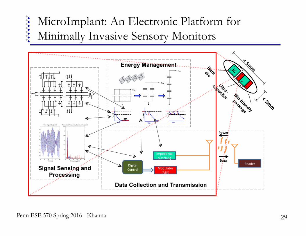
MicroImplant: An Electronic Platform for Minimally Invasive Sensory Monitors
29 Penn ESE 570 Spring 2016 - Khanna
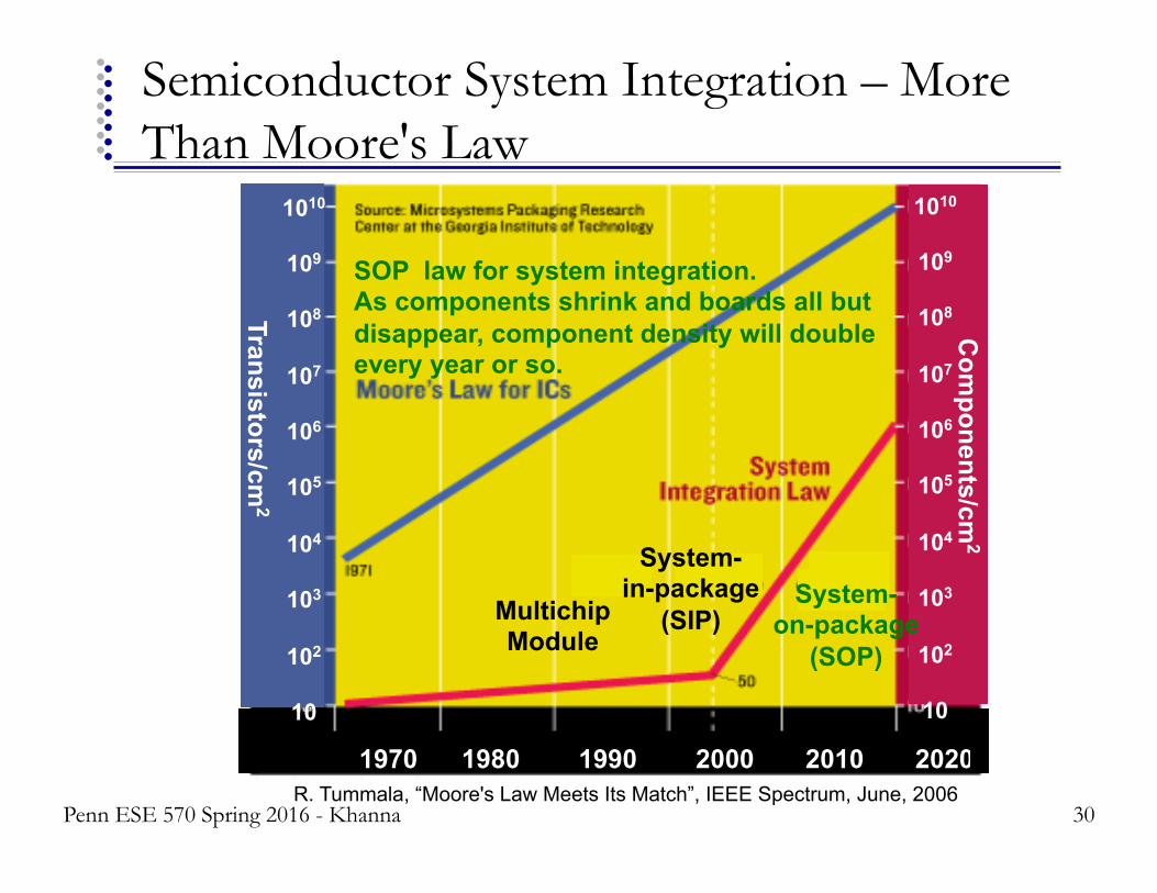
Semiconductor System Integration – More Than Moore's Law
30
1010
109
108
107
106
105
104
103
102
10
Transistors/cm2
1010
109
108
107
106
105
104
103
102
10
Com
ponents/cm2
1970 1980 1990 2000 2010 2020
Multichip Module
System- in-package
(SIP) System-
on-package (SOP)
R. Tummala, “Moore's Law Meets Its Match”, IEEE Spectrum, June, 2006
SOP law for system integration. As components shrink and boards all but disappear, component density will double every year or so.
Penn ESE 570 Spring 2016 - Khanna
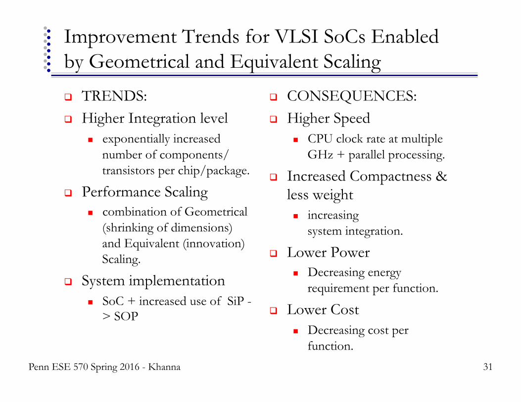
Improvement Trends for VLSI SoCs Enabled by Geometrical and Equivalent Scaling
! TRENDS: ! Higher Integration level
" exponentially increased number of components/transistors per chip/package.
! Performance Scaling " combination of Geometrical
(shrinking of dimensions) and Equivalent (innovation) Scaling.
! System implementation " SoC + increased use of SiP -
> SOP
! CONSEQUENCES: ! Higher Speed
" CPU clock rate at multiple GHz + parallel processing.
! Increased Compactness & less weight " increasing
system integration.
! Lower Power " Decreasing energy
requirement per function.
! Lower Cost " Decreasing cost per
function.
31 Penn ESE 570 Spring 2016 - Khanna
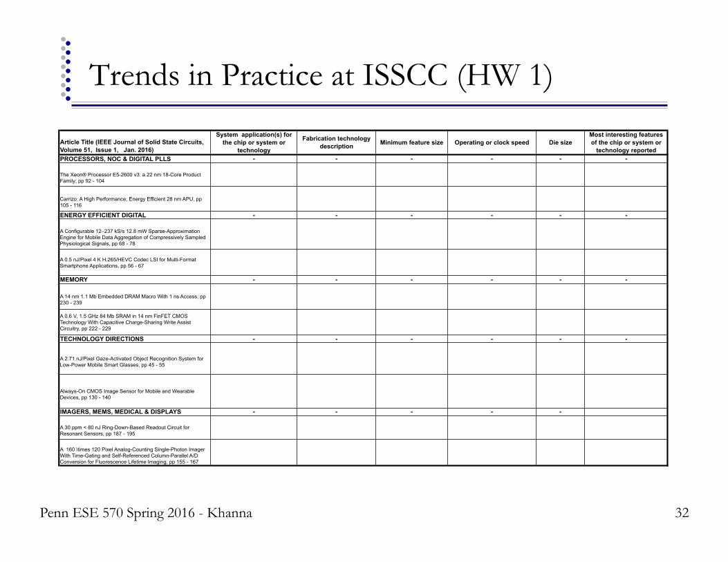
Trends in Practice at ISSCC (HW 1)
32 Penn ESE 570 Spring 2016 - Khanna
Article Title (IEEE Journal of Solid State Circuits, Volume 51, Issue 1, Jan. 2016)
System application(s) for the chip or system or
technology
Fabrication technology description Minimum feature size Operating or clock speed Die size
Most interesting features of the chip or system or
technology reportedPROCESSORS, NOC & DIGITAL PLLS - - - - - -
The Xeon® Processor E5-2600 v3: a 22 nm 18-Core Product Family; pp 92 - 104
Carrizo: A High Performance, Energy Efficient 28 nm APU, pp 105 - 116
ENERGY EFFICIENT DIGITAL - - - - - -
A Configurable 12–237 kS/s 12.8 mW Sparse-Approximation Engine for Mobile Data Aggregation of Compressively Sampled Physiological Signals, pp 68 - 78
A 0.5 nJ/Pixel 4 K H.265/HEVC Codec LSI for Multi-Format Smartphone Applications, pp 56 - 67
MEMORY - - - - - -
A 14 nm 1.1 Mb Embedded DRAM Macro With 1 ns Access, pp 230 - 239
A 0.6 V, 1.5 GHz 84 Mb SRAM in 14 nm FinFET CMOS Technology With Capacitive Charge-Sharing Write Assist Circuitry, pp 222 - 229
TECHNOLOGY DIRECTIONS - - - - - -
A 2.71 nJ/Pixel Gaze-Activated Object Recognition System for Low-Power Mobile Smart Glasses, pp 45 - 55
Always-On CMOS Image Sensor for Mobile and Wearable Devices, pp 130 - 140
IMAGERS, MEMS, MEDICAL & DISPLAYS - - - - -
A 30 ppm < 80 nJ Ring-Down-Based Readout Circuit for Resonant Sensors, pp 187 - 195
A 160 \times 120 Pixel Analog-Counting Single-Photon Imager With Time-Gating and Self-Referenced Column-Parallel A/D Conversion for Fluorescence Lifetime Imaging, pp 155 - 167
Design Example
Penn ESE 570 Spring 2016 - Khanna
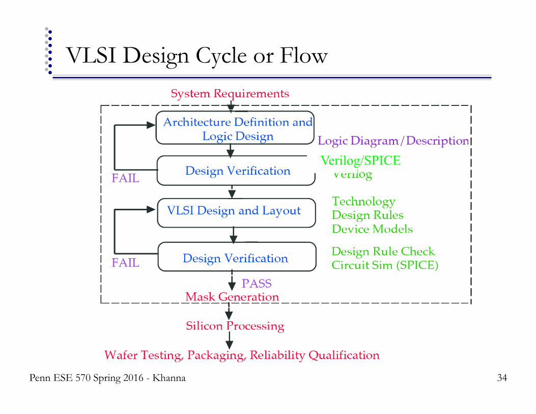
VLSI Design Cycle or Flow
34
Verilog/SPICE
Penn ESE 570 Spring 2016 - Khanna
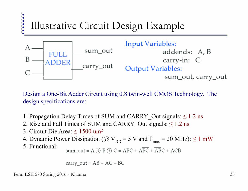
Illustrative Circuit Design Example
35
Design a One-Bit Adder Circuit using 0.8 twin-well CMOS Technology. The design specifications are: 1. Propagation Delay Times of SUM and CARRY_Out signals: ≤ 1.2 ns 2. Rise and Fall Times of SUM and CARRY_Out signals: ≤ 1.2 ns 3. Circuit Die Area: ≤ 1500 um2
4. Dynamic Power Dissipation (@ VDD = 5 V and f max = 20 MHz): ≤ 1 mW 5. Functional:
Penn ESE 570 Spring 2016 - Khanna
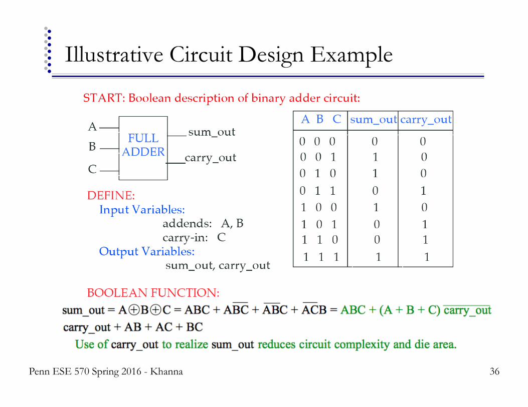
Illustrative Circuit Design Example
36 Penn ESE 570 Spring 2016 - Khanna
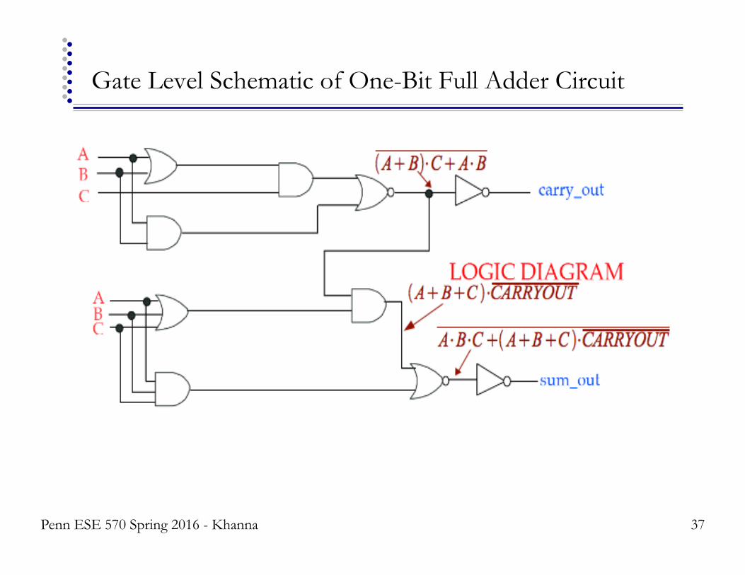
Gate Level Schematic of One-Bit Full Adder Circuit
37 Penn ESE 570 Spring 2016 - Khanna
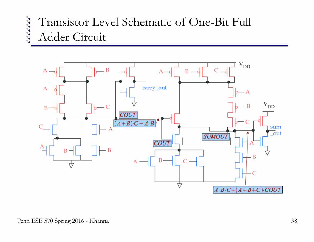
Transistor Level Schematic of One-Bit Full Adder Circuit
38 Penn ESE 570 Spring 2016 - Khanna
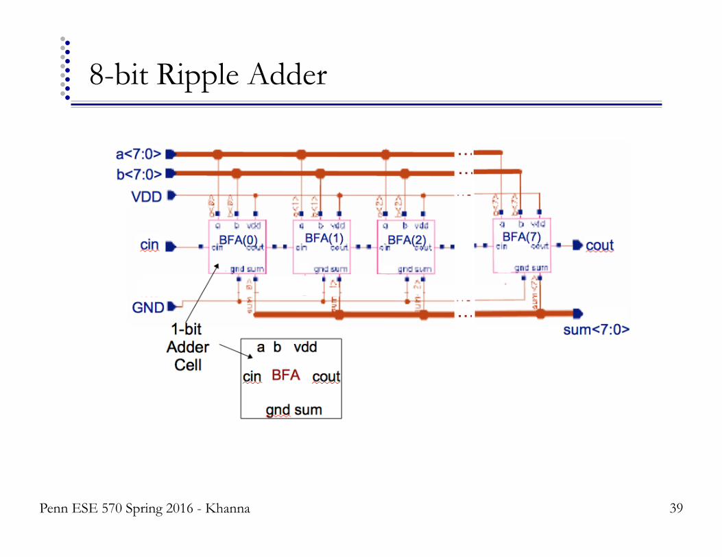
8-bit Ripple Adder
39 Penn ESE 570 Spring 2016 - Khanna

Initial Layout of One-Bit Full Adder Circuit
40
N1 N2
N1 N2
SUMOUTCOUT
COUT
Penn ESE 570 Spring 2016 - Khanna
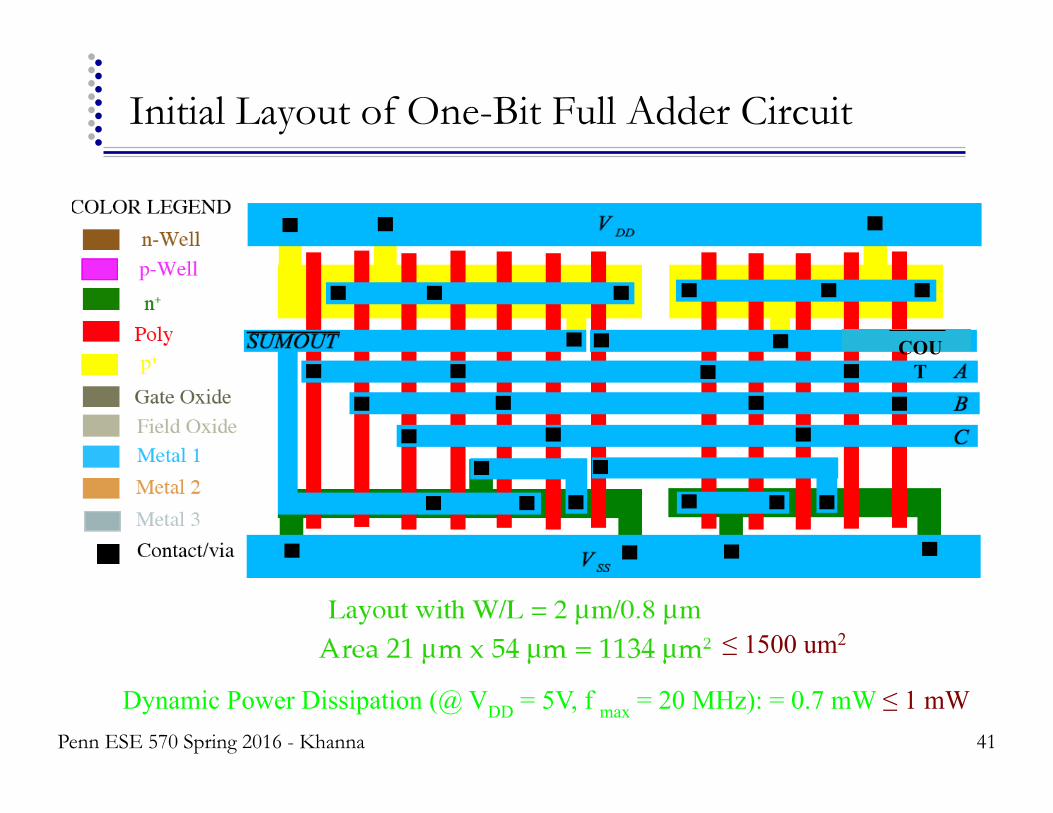
Initial Layout of One-Bit Full Adder Circuit
41
COUT
Dynamic Power Dissipation (@ VDD = 5V, f max = 20 MHz): = 0.7 mW ≤ 1 mW
≤ 1500 um2
Penn ESE 570 Spring 2016 - Khanna
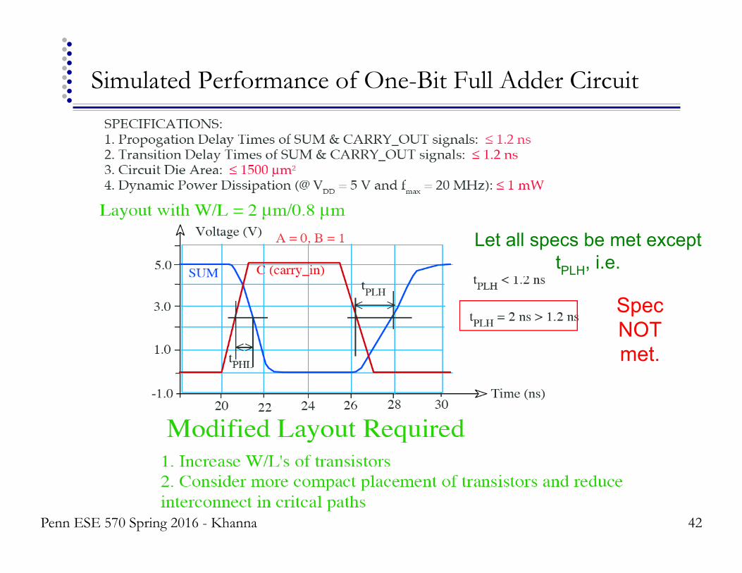
Simulated Performance of One-Bit Full Adder Circuit
42
Spec NOT met.
Let all specs be met except tPLH, i.e.
Penn ESE 570 Spring 2016 - Khanna