enhancing long-term reliability with copper leadframes · enhancing long-term reliability with...
TRANSCRIPT
1940 Zanker Rd. • San Jose, CA. 95112 • Tel: 408.969.6600 • E-mail: [email protected] • www.issi.com
Enhancing Long-Term Reliability with Copper LeadframesOne of the points to consider when selecting a semiconductor device is the package reliability, relative to the expected operating conditions of the electronics application. With this in mind, ISSI now includes synchronous DRAMs to its extensive portfolio of SRAM products offered in copper leadframes. Most DRAMs and SRAMs currently available in TSOP use Alloy42 leadframes. The use of the copper material can enhance long-term field reliability by contributing to the durability of solder joints, and improving thermal dissipation. Moreover, the solder plating on the leads of the DRAM is Nickel-Palladium-Gold, eliminating the concern of whisker growth. These characteristics are especially important in automotive, medical, industrial, and telecom applications, where a long-life of trouble-free operation is a vital concern.
Better Joint Reliability
During the service life of an electronics system, the printed circuit board (PCB) and the soldered components may be subjected to repeated thermal changes over a period of time. Many applications are expected to work reliably despite temperature variations from as low as -40°C to as high as 85°C or 125°C. This is a realistic range for an automotive engine control system. A system problem can arise because every type of material on the surface of that board has a different responsiveness to temperature, which is defined by its coefficient of thermal expansion (CTE). This expansion and contraction property applies to the board, the metallic traces
carrying signals and power, and all the passive and active components soldered to the board. The differing expansion rates can result in pushing and pulling stresses being concentrated at the points where they interface, which are often the solder joints. Joints tend to have some resiliency initially and maintain their electrical pathways. However, the effects of the stress may accumulate to the point that a crack appears, causing an electrical discontinuity.
The TSOP package continues to be popular because of its relatively small footprint, low profile, and low cost. In the
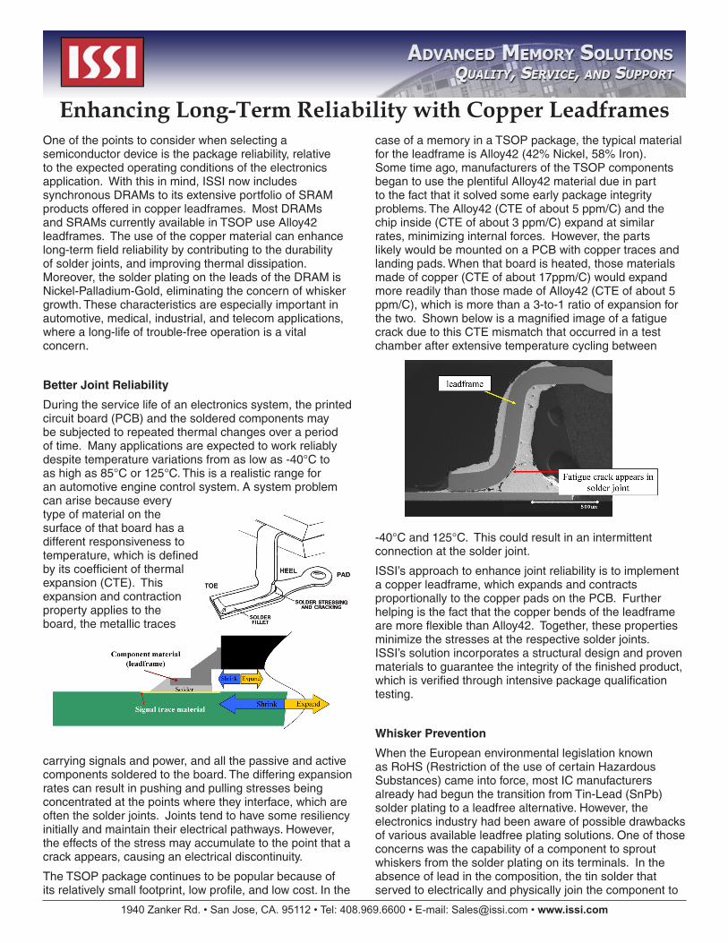
case of a memory in a TSOP package, the typical material for the leadframe is Alloy42 (42% Nickel, 58% Iron). Some time ago, manufacturers of the TSOP components began to use the plentiful Alloy42 material due in part to the fact that it solved some early package integrity problems. The Alloy42 (CTE of about 5 ppm/C) and the chip inside (CTE of about 3 ppm/C) expand at similar rates, minimizing internal forces. However, the parts likely would be mounted on a PCB with copper traces and landing pads. When that board is heated, those materials made of copper (CTE of about 17ppm/C) would expand more readily than those made of Alloy42 (CTE of about 5 ppm/C), which is more than a 3-to-1 ratio of expansion for the two. Shown below is a magnified image of a fatigue crack due to this CTE mismatch that occurred in a test chamber after extensive temperature cycling between
-40°C and 125°C. This could result in an intermittent connection at the solder joint.
ISSI’s approach to enhance joint reliability is to implement a copper leadframe, which expands and contracts proportionally to the copper pads on the PCB. Further helping is the fact that the copper bends of the leadframe are more flexible than Alloy42. Together, these properties minimize the stresses at the respective solder joints. ISSI’s solution incorporates a structural design and proven materials to guarantee the integrity of the finished product, which is verified through intensive package qualification testing.
Whisker Prevention
When the European environmental legislation known as RoHS (Restriction of the use of certain Hazardous Substances) came into force, most IC manufacturers already had begun the transition from Tin-Lead (SnPb) solder plating to a leadfree alternative. However, the electronics industry had been aware of possible drawbacks of various available leadfree plating solutions. One of those concerns was the capability of a component to sprout whiskers from the solder plating on its terminals. In the absence of lead in the composition, the tin solder that served to electrically and physically join the component to

Whiskers forming on anonymous part (Photo by NASA)
If a whisker bridges this gap across the pins, or it breaks, there could be a short-circuit and a system could fail. (Photo by NASA)
1940 Zanker Rd. • San Jose, CA. 95112 • Tel: 408.969.6600 • E-mail: [email protected] • www.issi.com
the board sometimes was prone to develop microscopic metal filaments under certain circumstances, and they might grow indefinitely. If not prevented, the whiskers could bridge metal contacts, and cause a short circuit or even an explosive power surge. Tin whiskers have been the culprit in dooming a variety of electronics in the field—or in space. Several of the more well-known failures have occurred with expensive communications satellites, sometimes at a cost of over $200M.
The exact mechanisms of whisker formation are complex, and are not completely understood, but identified contributors may include: the environmental conditions, the materials chosen, the solder plating process, and the board-level processes or decisions. Fortunately, there are methods to analyze and reduce the potential risk of this happening. ISSI’s standard leadfree plating material is pure matte Tin (Sn), a widely used and effective RoHS compliant plating option for integrated circuit components. One of the whisker mitigation methods recommended by JEDEC for this type of material is annealing: during production, all ISSI pure matte tin parts are annealed for 1 hour at 150°C within 24 hours of plating. This technique could reduce the likelihood and degree of later whisker
environmental stress, followed by magnification of the plating surfaces for measurement.
The electronics industry generally accepts the annealed matte tin plating solution. However, the organization iNEMI (International Electronics Manufacturing Initiative) lists Nickel-Palladium-Gold (NiPdAu) as the most preferred plating material, due to the elimination of risk for whiskers. ISSI has selected this plating type for its new offering of copper leadframe DRAMs for those systems without any tolerance of whisker potential.
Better Thermal Dissipation
The use of a copper leadframe for the ISSI memory in a TSOP package carries the additional benefit of reducing the thermal resistance of the component, as heat transfers more quickly within. The thermal conductivity of copper is 170W/m.K, while that of Alloy42 is about 12 times less: only 14W/m.K. This translates to better heat dissipation from the chip to leadframe, which releases eventually to the air, and therefore less heat stress remains inside the component. Heat stress at the chip is one of the leading causes of a non-mechanical component failure in a long life application. In theory, the higher the temperature level within the part, the shorter the lifespan of a part, as the internal circuitry can be subject to wear-out.
In order to illustrate the thermal dissipating abilities of a memory component based on the two types of leadframes, a software simulation was conducted using the known properties of the materials. An extreme, yet possible hypothetical set of conditions was assumed, and the temperature gradients of the two components were graphed side-by-side.
The table below uses those properties to calculate qja (die to ambient thermal resistance), assuming a 4-layer PCB and 0 m/s airflow. Thermal conductivity is listed for reference.
Thermal conductivity (W/m.K) qja (C/W)
Alloy 42 14 89
Copper 170 52
Notes: The calculation of qja (“theta-ja”) is beyond the scope of this discussion. Other factors besides the qja play a role in enhancement of heat dissipation.
formation by diffusing and relieving localized stresses within the microscopic structures of the solder metal. To verify acceptance of the finished components, ISSI conforms to the JEDEC “JESD201 - Class 2” specification, which includes periodically subjecting the parts to
1940 Zanker Rd. • San Jose, CA. 95112 • Tel: 408.969.6600 • E-mail: [email protected] • www.issi.com
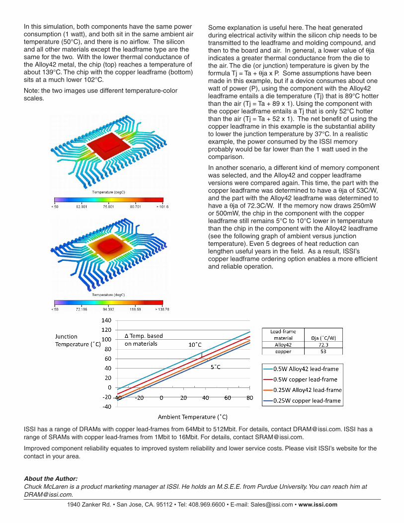
In this simulation, both components have the same power consumption (1 watt), and both sit in the same ambient air temperature (50°C), and there is no airflow. The silicon and all other materials except the leadframe type are the same for the two. With the lower thermal conductance of the Alloy42 metal, the chip (top) reaches a temperature of about 139°C. The chip with the copper leadframe (bottom) sits at a much lower 102°C.
Note: the two images use different temperature-color scales.
Some explanation is useful here. The heat generated during electrical activity within the silicon chip needs to be transmitted to the leadframe and molding compound, and then to the board and air. In general, a lower value of qja indicates a greater thermal conductance from the die to the air. The die (or junction) temperature is given by the formula Tj = Ta + qja x P. Some assumptions have been made in this example, but if a device consumes about one watt of power (P), using the component with the Alloy42 leadframe entails a die temperature (Tj) that is 89°C hotter than the air (Tj = Ta + 89 x 1). Using the component with the copper leadframe entails a Tj that is only 52°C hotter than the air (Tj = Ta + 52 x 1). The net benefit of using the copper leadframe in this example is the substantial ability to lower the junction temperature by 37°C. In a realistic example, the power consumed by the ISSI memory probably would be far lower than the 1 watt used in the comparison.
In another scenario, a different kind of memory component was selected, and the Alloy42 and copper leadframe versions were compared again. This time, the part with the copper leadframe was determined to have a qja of 53C/W, and the part with the Alloy42 leadframe was determined to have a qja of 72.3C/W. If the memory now draws 250mW or 500mW, the chip in the component with the copper leadframe still remains 5°C to 10°C lower in temperature than the chip in the component with the Alloy42 leadframe (see the following graph of ambient versus junction temperature). Even 5 degrees of heat reduction can lengthen useful years in the field. As a result, ISSI’s copper leadframe ordering option enables a more efficient and reliable operation.
ISSI has a range of DRAMs with copper lead-frames from 64Mbit to 512Mbit. For details, contact [email protected]. ISSI has a range of SRAMs with copper lead-frames from 1Mbit to 16Mbit. For details, contact [email protected].
Improved component reliability equates to improved system reliability and lower service costs. Please visit ISSI’s website for the contact in your area.
About the Author: Chuck McLaren is a product marketing manager at ISSI. He holds an M.S.E.E. from Purdue University. You can reach him at [email protected].