energia- ja geotehnika doktorikool ii...
TRANSCRIPT
ELEKTRIAJAMITE JA JÕUELEKTROONIKA INSTITUUT
ENERGIA- JA GEOTEHNIKA DOKTORIKOOL II
INTENSIIVKURSUS
"FPGA BASED CONTROL SOLUTIONS FOR SPECIFIC POWER CONVERTERS"
Prof. ILYA GALKIN, Riga Technical University
Tallinn 2012

Page 1 of 38
FPGA Based Control Solutions for Specific Power Converters (course material)
(Prof. Ilya GALKIN, Riga Technical University, [email protected])
Table of Contents
Table of Contents ..................................................................................................................................... 1
1. Introduction ..................................................................................................................................... 2
Problem of Specific Control Task ................................................................................................. 2
Other Power Converters with Complicated Control ................................................................... 3
Training Task ................................................................................................................................ 5
2. Single-Ended Primary Inductor Converter ....................................................................................... 7
Genesis, Schematic and Operation of SEPIC ............................................................................... 7
Choice of elements for SEPIC ...................................................................................................... 8
SEPIC Converter of Training Kit .................................................................................................10
3. Interleaved Control of Power Converters ......................................................................................11
Basics of Interleaved Control .....................................................................................................11
Obtaining the Interleaved Control Signals from Programmable Logic ......................................13
4. Getting Analog Data through SPI Interface ....................................................................................18
Main Features of SPI ..................................................................................................................18
Communication of Programmable Logic and SPI ......................................................................20
5. Features of P and PI regulators made with FPGA ..........................................................................24
Appendix A: VHDL Quick Reference .......................................................................................................27
Appendix B: Layout and Connections of FPGA Training Kit ...................................................................34
Layout of Cyclone III FPGA Training Kit .....................................................................................34
Connections of Cyclone III FPGA Training Kit ............................................................................34
Appendix C: Schematics of FPGA Training Kit ........................................................................................35
Main Board ................................................................................................................................35
FPGA Cyclone III Target Board ...................................................................................................36
SEPIC Module.............................................................................................................................37
References ..............................................................................................................................................38
FPGA Based Control Solutions for Specific Power Converters
Page 2 of 38
1. Introduction
Problem of Specific Control Task
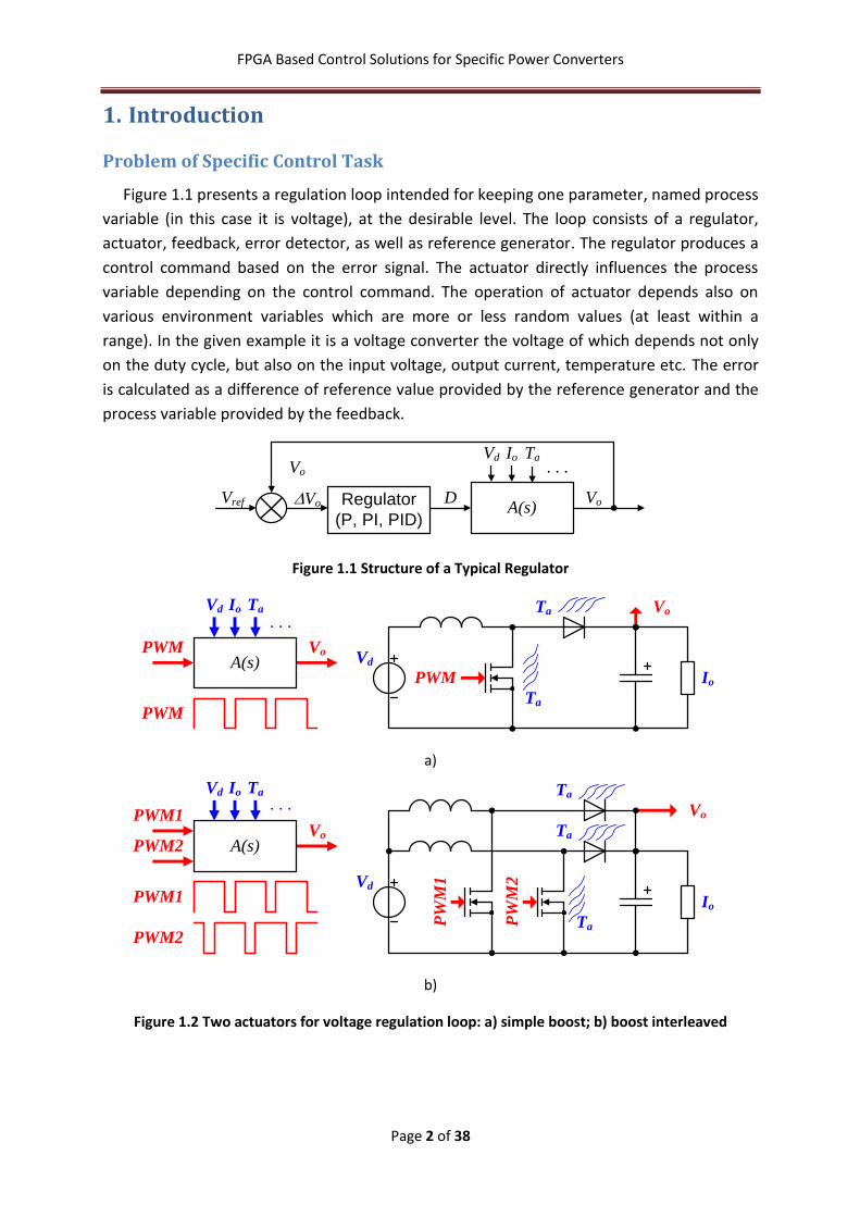
Figure 1.1 presents a regulation loop intended for keeping one parameter, named process
variable (in this case it is voltage), at the desirable level. The loop consists of a regulator,
actuator, feedback, error detector, as well as reference generator. The regulator produces a
control command based on the error signal. The actuator directly influences the process
variable depending on the control command. The operation of actuator depends also on
various environment variables which are more or less random values (at least within a
range). In the given example it is a voltage converter the voltage of which depends not only
on the duty cycle, but also on the input voltage, output current, temperature etc. The error
is calculated as a difference of reference value provided by the reference generator and the
process variable provided by the feedback.
Vd
. . .
A(s)
Io
D VoRegulator
(P, PI, PID)
Vref
Vo
DVo
Ta
Figure 1.1 Structure of a Typical Regulator
A(s)PWM Vo
Vd
. . . Io
PWM
VoTa
Vd
Io
Ta
Ta
PWM
a)
A(s)
PWM1Vo
Vd
. . . Io
PW
M1
Vo
Ta
Vd
Io
Ta
Ta
PWM1
PWM2
PWM2
Ta
PW
M2
b)
Figure 1.2 Two actuators for voltage regulation loop: a) simple boost; b) boost interleaved
FPGA Based Control Solutions for Specific Power Converters
Page 3 of 38
DRegulator
(P, PI, PID)
Vref_MCU
Vo_MCU
DVo_MCU Timer0_A2+
compare f.
Voltage
sensor ADC10
Vo_sensVo_MCU
Cmd
MSP430G2231
Software MSP430G2231
PeripheralsVd
. . .
A(s)
Io
Vo
Ta
MCU MSP430G2231
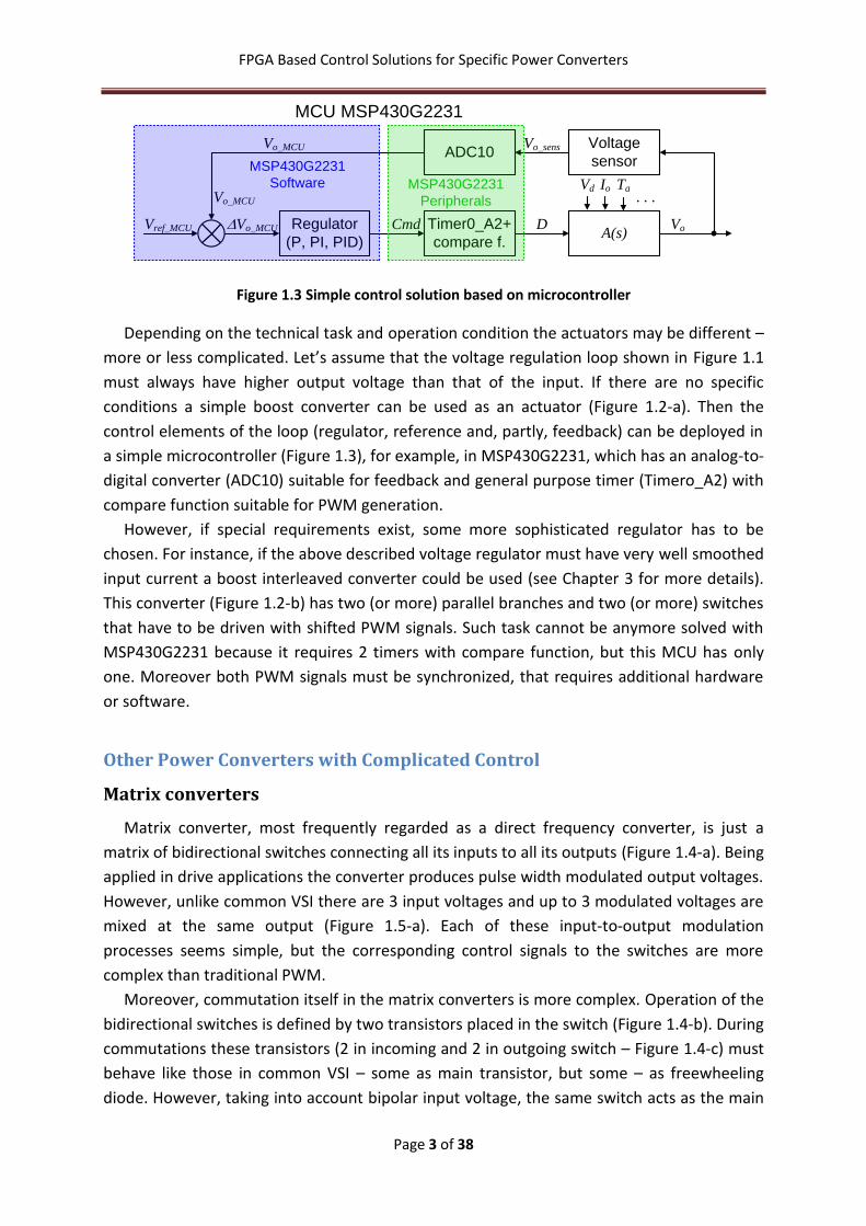
Figure 1.3 Simple control solution based on microcontroller
Depending on the technical task and operation condition the actuators may be different –
more or less complicated. Let’s assume that the voltage regulation loop shown in Figure 1.1
must always have higher output voltage than that of the input. If there are no specific
conditions a simple boost converter can be used as an actuator (Figure 1.2-a). Then the
control elements of the loop (regulator, reference and, partly, feedback) can be deployed in
a simple microcontroller (Figure 1.3), for example, in MSP430G2231, which has an analog-to-
digital converter (ADC10) suitable for feedback and general purpose timer (Timero_A2) with
compare function suitable for PWM generation.
However, if special requirements exist, some more sophisticated regulator has to be
chosen. For instance, if the above described voltage regulator must have very well smoothed
input current a boost interleaved converter could be used (see Chapter 3 for more details).
This converter (Figure 1.2-b) has two (or more) parallel branches and two (or more) switches
that have to be driven with shifted PWM signals. Such task cannot be anymore solved with
MSP430G2231 because it requires 2 timers with compare function, but this MCU has only
one. Moreover both PWM signals must be synchronized, that requires additional hardware
or software.
Other Power Converters with Complicated Control
Matrix converters
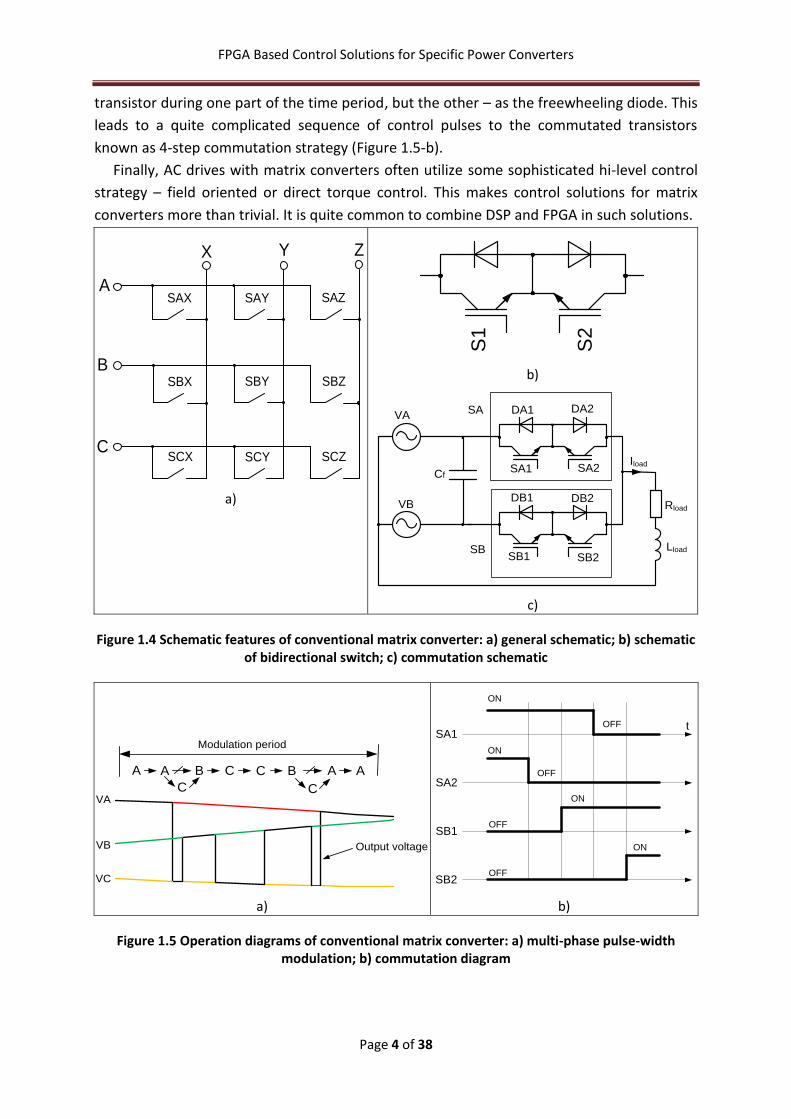
Matrix converter, most frequently regarded as a direct frequency converter, is just a
matrix of bidirectional switches connecting all its inputs to all its outputs (Figure 1.4-a). Being
applied in drive applications the converter produces pulse width modulated output voltages.
However, unlike common VSI there are 3 input voltages and up to 3 modulated voltages are
mixed at the same output (Figure 1.5-a). Each of these input-to-output modulation
processes seems simple, but the corresponding control signals to the switches are more
complex than traditional PWM.
Moreover, commutation itself in the matrix converters is more complex. Operation of the
bidirectional switches is defined by two transistors placed in the switch (Figure 1.4-b). During
commutations these transistors (2 in incoming and 2 in outgoing switch – Figure 1.4-c) must
behave like those in common VSI – some as main transistor, but some – as freewheeling
diode. However, taking into account bipolar input voltage, the same switch acts as the main
FPGA Based Control Solutions for Specific Power Converters
Page 4 of 38
transistor during one part of the time period, but the other – as the freewheeling diode. This
leads to a quite complicated sequence of control pulses to the commutated transistors
known as 4-step commutation strategy (Figure 1.5-b).
Finally, AC drives with matrix converters often utilize some sophisticated hi-level control
strategy – field oriented or direct torque control. This makes control solutions for matrix
converters more than trivial. It is quite common to combine DSP and FPGA in such solutions.
A
B
C
X Y Z
SAY SAZ
SBY SBZ
SCX SCY SCZ
SAX
SBX
a)
S1
S2
b)
Rload
SA1
SB1
VA
Cf
VB
SA2
SB2
DB1 DB2
DA1 DA2
Lload
SA
SB
Iload
c)
Figure 1.4 Schematic features of conventional matrix converter: a) general schematic; b) schematic of bidirectional switch; c) commutation schematic
Output voltage
VA
VB
VC
Modulation period
A A B C C
C
B A A
C
a)
SA1
SA2
SB1
SB2
t
ON
ON
ON
ON
OFF
OFF
OFF
OFF
b)
Figure 1.5 Operation diagrams of conventional matrix converter: a) multi-phase pulse-width modulation; b) commutation diagram

FPGA Based Control Solutions for Specific Power Converters
Page 5 of 38
Multilevel Converters
One mode power converter requiring specific control solution – is multilevel converter. A
diode clamped version of three-level converter is given in Figure 1.6-a, but its output phase
voltage - in Figure 1.6-b. In such converters additional voltage levels are formed with the
help of capacitor divider. Some control strategies assume that during certain intervals the
switches are constantly off, during the others - constantly on, but may be also pulse-width
modulated, as well as specific dead times of shoot-through states may appear. Again this is
not a trivial task that can be solved with a common interval timer and compare module.
S10
S11
S6
S7
S4
S3
3 PHASE
DRIVE
M
Cf1
DC-LINK MULTI-LEVEL-INVERTER
Cf2
S1
S2
S8
S5
S12
S9
D1
D2
D3
D4
D5
D6
a)
-450
-300
-150
0
150
300
450
0 0,005 0,01 0,015 0,02 0,025 0,03 0,035Vo
ut,
[V]
t, [s]
b)
Figure 1.6 Schematic (a) and operation diagram (b) of diode clamped multilevel converter
Training Assignment
In the given material a closed loop voltage regulation system for LED lighting application
is discussed. It is known that LEDs brightness is almost proportional to their current that, in
turn, is defined by the voltage applied to the LEDs as well as on their VA-curve. So in simple
FPGA Based Control Solutions for Specific Power Converters
Page 6 of 38
occasion it is possible to adjust the light, produced by LEDs by means of applying to them an
adjustable voltage.
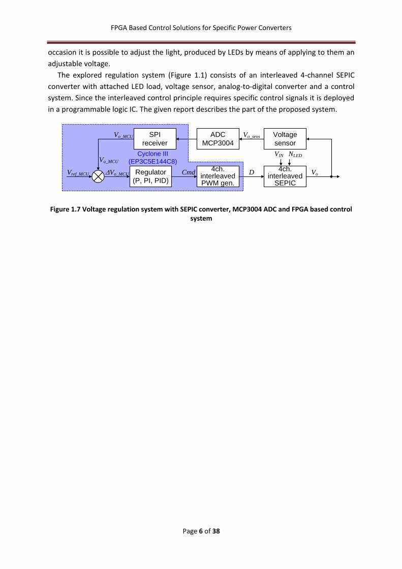
The explored regulation system (Figure 1.1) consists of an interleaved 4-channel SEPIC
converter with attached LED load, voltage sensor, analog-to-digital converter and a control
system. Since the interleaved control principle requires specific control signals it is deployed
in a programmable logic IC. The given report describes the part of the proposed system.
DRegulator
(P, PI, PID)
Vref_MCU
Vo_MCU
DVo_MCU4ch.
interleaved PWM gen.
Voltage
sensor
ADC
MCP3004
Vo_sensVo_MCU
Cmd
Cyclone III
(EP3C5E144C8)VIN
4ch. interleaved
SEPIC
NLED
Vo
SPI
receiver
Figure 1.7 Voltage regulation system with SEPIC converter, MCP3004 ADC and FPGA based control system

FPGA Based Control Solutions for Specific Power Converters
Page 7 of 38
2. Single-Ended Primary Inductor Converter
Genesis, Schematic and Operation of SEPIC
The converter utilized in the course is called Single-Ended Primary Inductor Converter
(SEPIC). In order to synthesize a SEPIC converter let’s imagine a buck/boost circuit supplied
from a large capacitor C. If positive output voltage is required then the polarity of the input
capacitor (source) has also to be changed (green area in Figure 2.1-a). The capacitor,
however, cannot supply the circuit and its load forever. It has to be recharged from a voltage
source, which can be attached as it is shown in the yellow area in Figure 2.1-a. The additional
inductor L1 is necessary to avoid a short-circuit of the source. The return of the source could
be attached to the point (a), but simpler driver is possible if it is connected to the common
ground. The above considerations form a valid SEPIC circuit given in Figure 2.1.
VIN
+
– VO
RL
OA
D
+
–
L1
S
D
L2
+ –
CO
buck/boostC
(a)
a)
D
VIN
+
– VO
RL
OA
D
+
–
L1
S L2
+ –C
CO
I II III
b)
SVIN
+
– VO
RL
OA
D
+
–
L1 D
L2
+ –
CO
C
c)
Figure 2.1 Schematic of single-ended primary inductor converter: 1) genesis; 2) current paths if switch is connected; 3) current path if switch is disconnected

FPGA Based Control Solutions for Specific Power Converters
Page 8 of 38
The converter given in Figure 2.1 has two stages of operation in the continuous
conduction mode. The first one takes place while the controllable switch S of the converter
is on. Then the circuit in fact is split into three independent loops: 1) the input source
charges inductor L1; 2) the internal capacitor C charges inductor L2 and 3) the output
capacitor CO supplies the load of the converter (Figure 2.1-b). The second stage starts as
soon as the switch S is turned off. Then the input source and input inductor L1 in one branch
as well as the indictor L2 in the second branch together feed the output capacitor CO and the
load. The internal capacitor C is being discharged during this time (Figure 2.1-c).
The static equation of SEPIC converter can be derived from the voltage balance equation
of the inductor L2. While the switch S is on this inductor is attached to the internal capacitor
C with voltage VC. During the second stage, when the switch S is off and currents are
conducted by the diode D this inductor is tied to the output capacitor CO with voltage VO.
Then the average voltage over this inductor that within a commutation period must be 0
looks as:
0TD)(1)V(TDV OC , (2.1)
where: T – is commutation period and D – duty cycle. (2.1) can be rewritten as:
CO VD1
DV
. (2.2)
At the same time it is possible to write Kirchhoff’s voltage law for the average voltages of the
loop VIN, L1, C, L2. Taking into account that the average voltages of the inductors must be 0,
this gives:
CCL2aCL1aIN V0V0VVVV (2.3)
that, in turns, gives the static equation of buck/boost converter:
INCO VD1
DVV
. (2.4)
The latter equation proves that SEPIC is essentially buck/boost converter without voltage
sign inversion. It also indicates that the switch of SEPIC cannot be left in the on-state (this is
a short circuit at D=1), as well as that the converter cannot operate without any load.
Choice of elements for SEPIC
Maximal Duty Cycle
A simplified selection procedure for SEPIC elements is given below [1]. First of all the
maximal value of the duty cycle DR has to be calculated. The corresponding equation
following from (2.2) is
OINmin
Omax
VV
VD
(2.5)
or more accurately
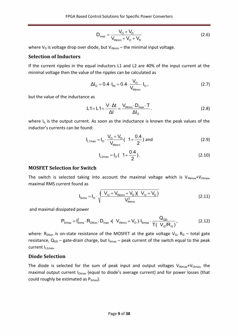
FPGA Based Control Solutions for Specific Power Converters
Page 9 of 38
DOINmin
DOmax
VVV
VVD
(2.6)
where VD is voltage drop over diode, but VINmin – the minimal input voltage.
Selection of Inductors
If the current ripples in the equal inductors L1 and L2 are 40% of the input current at the
minimal voltage then the value of the ripples can be calculated as
O
INmin
OINO I
V
V0.4I0.4ΔI , (2.7)
but the value of the inductance as
O
maxINmin
ΔI
TDV
ΔI
ΔtVL1L1
. (2.8)
where Io is the output current. As soon as the inductance is known the peak values of the
inductor’s currents can be found:
)2
0.4(1
V
VVII
INmin
DOOL1max
and (2.9)
)2
0.4(1II OL2max . (2.10)
MOSFET Selection for Switch
The switch is selected taking into account the maximal voltage which is VINmax+VOmax,
maximal RMS current found as
2
INmin
DODINminOOSrms
V
)V(V)VV(VII
(2.11)
and maximal dissipated power
)/R(VT
QI)V(VDRIP
GG
GDSmaxOINminmaxDSon
2
SrmsSmax
, (2.12)
where: RDSon is on-state resistance of the MOSFET at the gate voltage VG, RG – total gate
resistance, QGD – gate-drain charge, but ISmax – peak current of the switch equal to the peak
current IL1max.
Diode Selection
The diode is selected for the sum of peak input and output voltages VINmax+VOmax, the
maximal output current IOmax (equal to diode’s average current) and for power losses (that
could roughly be estimated as PSmax).

FPGA Based Control Solutions for Specific Power Converters
Page 10 of 38
C
RloadD
iD(t) io(t)
ico(t)
a)
iC(t)
–Io t+DQ
toff
–DQ
ton
b)
Figure 2.2 Current ripples in output capacitor of SEPIC converter: a) schematic of the output node; b) output capacitor’s current
Coupling Capacitor Selection
This capacitor is selected for the maximal input voltage VINmax, maximal RMS current
INmin
DOOCrms
V
VVII
(2.13)
and maximal voltage ripples
INmaxO
C 0.01VC
TDIΔV
. (2.14)
Output Capacitor Selection
In the similar way, the output capacitor is selected for the maximal output voltage VOmax,
maximal RMS current
INmin
DOOCOrms
V
VVII
(2.15)
and maximal voltage ripples
O
O
maxOO 0.01V
C0.5
TDIΔV
. (2.16)
Since the current through this capacitor due to the output diode (Figure 2.2-a) is pulse mode
current (Figure 2.2-b) the equivalent series resistance is also important for this capacitor:
O
minOESR
0.01V0.5
TDIR
. (2.17)
SEPIC Converter of Training Kit
The provided training kit includes a SEPIC converter containing 4 parallel branches. It is
supplied for a laboratory power supply of 15…18V. The load – 15 branches of 6 LEDs of
3.2Vx0.12A and a ballast resistor of the same voltage drop. Therefore VOmax =21V, IOmax=1.8A.
The corresponding elements of SEPIC converter are: MOSFET – PHT4NQ10T, diode –
STTH2R02A, L1 and L2 – 820Hx1.5A, CO 2x270Fx63V and C – 10Fx25V. See “Appendix C:
Schematics of FPGA Training Kit” section “SEPIC Module” on page 37 for more details.
FPGA Based Control Solutions for Specific Power Converters
Page 11 of 38
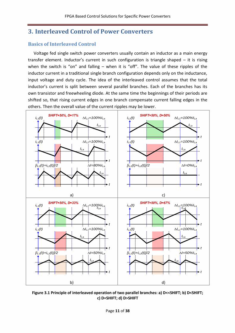
3. Interleaved Control of Power Converters
Basics of Interleaved Control
Voltage fed single switch power converters usually contain an inductor as a main energy
transfer element. Inductor’s current in such configuration is triangle shaped – it is rising
when the switch is “on” and falling – when it is “off”. The value of these ripples of the
inductor current in a traditional single branch configuration depends only on the inductance,
input voltage and duty cycle. The idea of the interleaved control assumes that the total
inductor’s current is split between several parallel branches. Each of the branches has its
own transistor and freewheeling diode. At the same time the beginnings of their periods are
shifted so, that rising current edges in one branch compensate current falling edges in the
others. Then the overall value of the current ripples may be lower.
[iL1(t)+iL2(t)]/2
iL1(t)
t
iL1(t)
t
t
ILa
ILa
ILa
∆IL1=100%ILa
∆IL2=100%ILa
∆I=80%ILa
SHIFT=50%, D=17%
a)
SHIFT=50%, D=50%
[iL1(t)+iL2(t)]/2
iL1(t)
t
iL1(t)
t
t
ILa
ILa
ILa
∆IL1=100%ILa
∆IL1=100%ILa
∆I=0%ILa
c)
SHIFT=50%, D=33%
[iL1(t)+iL2(t)]/2
iL1(t)
t
iL1(t)
t
t
ILa
ILa
ILa
∆IL1=100%ILa
∆IL1=100%ILa
∆I=50%ILa
b)
SHIFT=50%, D=67%
[iL1(t)+iL2(t)]/2
iL1(t)
t
iL1(t)
t
t
ILa
ILa
ILa
∆IL1=100%ILa
∆IL1=100%ILa
∆I=50%ILa
d)
Figure 3.1 Principle of interleaved operation of two parallel branches: a) D<<SHIFT; b) D<SHIFT; c) D=SHIFT; d) D>SHIFT

FPGA Based Control Solutions for Specific Power Converters
Page 12 of 38
If the number of branches is BR then the optimal shift can be found as
100%/BRSHIFT . (3.1)
The optimal value of the duty cycle is either the same or can be found as
SHIFT100%DOPT . (3.2)
The closer the duty cycle is to its optimal value the lower are the current ripples. At the
optimal values of the duty cycle the current ripples are 0%.
The interleaved principle of control is applied to parallel branches (converters) if their
inductors are placed at the input and if well smoothed, DC like input current is required. This
is quite important, for example, if the converter is supplied from a photovoltaic element or a
fuel cell requiring constant load current to keep them at optimal operation point and to
achieve the maximal power. The converters with inductor at the input (boost, Čuk, SEPIC
etc.) with parallel branches and interleaved control provide such current without significant
input filter (or with a small one).
The interleaved principle also allows to reduce the size of the output capacitor if the
inductor is placed at the output (Figure 3.2-a). The voltage ripples of the output capacitor
are always proportional to the integrated capacitor’s current (charge). For the converters
with an inductor at the output (buck, Čuk, ZETA etc.) it can be found as a difference of the
output DC current and triangle current of the inductor (Figure 3.2-b). Then the lower
inductor current ripples directly lead to lower output voltage ripples (Figure 3.2-c). Therefore
the interleaved principle allows using smaller capacitors at the output.
Note that Čuk converter has inductors both at the input and output. That is why the
interleaved principle equally forms its input and output currents more smoothed.
C
RloadL2
iL2(t)io(t)
ic(t)
L1
iL1(t)
a)
iC(t)DIL
t+DQ
TSW/2–DQ
b)
t
vC(t)
Vo
DVo
c)
Figure 3.2 Impact of current ripples on the voltage ripples: a) schematic of the output node; b) output capacitor’s current; c) output capacitor’s voltage

FPGA Based Control Solutions for Specific Power Converters
Page 13 of 38
Obtaining the Interleaved Control Signals from Programmable Logic
Interleaved control of parallel power branches is possible with the help of shifted pulse
mode signals. In order to design a generator of several pulse mode signals with shift an
ordinary generator has to be built at first.
Common (Single Channel) Pulse Width Modulation
triangle
sawtooth
reference
PWM
a)
Rising edge
prescaler= prescaler+1
If prescaler= max
counter = counter+1
prescaler = 0
end
yes
no
c)
DIV=80k80MHz
reference
PW
M
Q0.
..11
R
CL 12
12
1kHz
12xDIP switch
sawtooth
compa-rator
clk
q
reset
A
B
A>B
switch
clk
b)
Figure 3.3 Ordinary single channel PWM signal generator: a) generalized diagram; b) typical example of digital implementation; c) algorithm of counter operation
D1
D2
A2
A1
1ms
1000ms=1s
t
t
Counter
D1
D2
D1
D2
D2>D1
Figure 3.4 Operation diagram of single channel PWM signal generator
FPGA Based Control Solutions for Specific Power Converters
Page 14 of 38
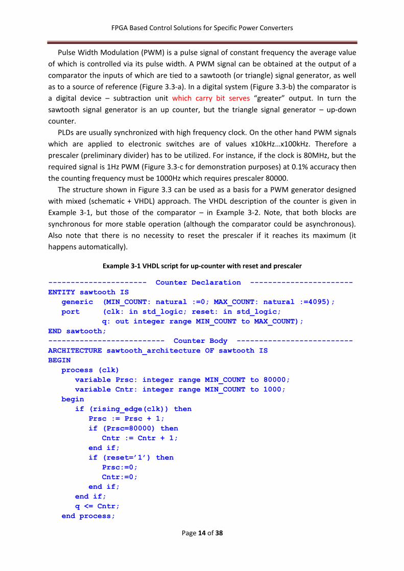
Pulse Width Modulation (PWM) is a pulse signal of constant frequency the average value
of which is controlled via its pulse width. A PWM signal can be obtained at the output of a
comparator the inputs of which are tied to a sawtooth (or triangle) signal generator, as well
as to a source of reference (Figure 3.3-a). In a digital system (Figure 3.3-b) the comparator is
a digital device – subtraction unit which carry bit serves “greater” output. In turn the
sawtooth signal generator is an up counter, but the triangle signal generator – up-down
counter.
PLDs are usually synchronized with high frequency clock. On the other hand PWM signals
which are applied to electronic switches are of values x10kHz…x100kHz. Therefore a
prescaler (preliminary divider) has to be utilized. For instance, if the clock is 80MHz, but the
required signal is 1Hz PWM (Figure 3.3-c for demonstration purposes) at 0.1% accuracy then
the counting frequency must be 1000Hz which requires prescaler 80000.
The structure shown in Figure 3.3 can be used as a basis for a PWM generator designed
with mixed (schematic + VHDL) approach. The VHDL description of the counter is given in
Example 3-1, but those of the comparator – in Example 3-2. Note, that both blocks are
synchronous for more stable operation (although the comparator could be asynchronous).
Also note that there is no necessity to reset the prescaler if it reaches its maximum (it
happens automatically).
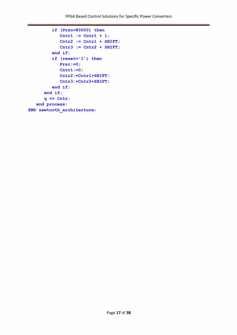
Example 3-1 VHDL script for up-counter with reset and prescaler
---------------------- Counter Declaration -----------------------
ENTITY sawtooth IS
generic (MIN_COUNT: natural :=0; MAX_COUNT: natural :=4095);
port (clk: in std_logic; reset: in std_logic;
q: out integer range MIN_COUNT to MAX_COUNT);
END sawtooth;
-------------------------- Counter Body --------------------------
ARCHITECTURE sawtooth_architecture OF sawtooth IS
BEGIN
process (clk)
variable Prsc: integer range MIN_COUNT to 80000;
variable Cntr: integer range MIN_COUNT to 1000;
begin
if (rising_edge(clk)) then
Prsc := Prsc + 1;
if (Prsc=80000) then
Cntr := Cntr + 1;
end if;
if (reset=’1’) then
Prsc:=0;
Cntr:=0;
end if;
end if;
q <= Cntr;
end process;

FPGA Based Control Solutions for Specific Power Converters
Page 15 of 38
END sawtooth_architecture;
Example 3-2 VHDL script for synchronous digital comparator
---------------- Digital Comparator Declaration ------------------
ENTITY comparator IS
port (
A: IN STD_LOGIC_VECTOR(11 downto 0);
B: IN STD_LOGIC_VECTOR(11 downto 0);
clk: IN STD_LOGIC;
Switch: OUT STD_LOGIC
);
END comparator;
-------------------- Digital Comparator Body ---------------------
ARCHITECTURE comparator_architecture OF comparator IS
BEGIN
process (clk)
begin
if (rising_edge(clk)) then
if (A >B) then Switch<='1'; else Switch<='0'; end if;
end if;
end process;
END comparator_architecture;
Multiple Channel Pulse Width Modulation with Shift
The most direct way to generate several shifted PWM signals is to obtain them from
several comparators tied to the same reference, but to different shifted sawtooth or triangle
signals. A three-channel example is shown in Figure 3.5-a. The corresponding digital system
has three comparators and three counters with a common clock. This approach is obviously
very extensive if the counters are independent. Then it requires as many times more flip-
flops as many channels have to be provided.
reference
PWM3
PWM2
sawtooth1
PWM1
sawtooth2
sawtooth3
a)
DIV=80k80MHz
reference
PWM1
Q0.
.11
RCL 12
12
1kHz
12xDIP switch
shift_
sawtooth
compa-rator
clk
q1
reset
A
B
A>B
switch
clk
q2
q3
12
12
PWM2
PWM3compa-rator
compa-ratorA
+B
A+B
333
667
b)

FPGA Based Control Solutions for Specific Power Converters
Page 16 of 38
Figure 3.5 Multiple channel shifted PWM signals generator: a) generalized diagram; b) typical example of digital implementation; c) operation diagram
D1
A
D3D2
t
t
Counter1
Counter1 = Counter1+333
Counter3 = Counter1+667
D1=D2=D3
Figure 3.6 Operation diagram of multiple channel shifted PWM signals generator
However, there is a different design approach that utilizes only one counter and adds the
proper shifts just on the corresponding output (Figure 3.5-b). At the same time this approach
has very simple VHDL description. All the considerations taking place in the case of single
channel PWM are valid also in the case of the described multi-channel generator. Certain
prescaler is necessary. Also the counter starts the next cycle of counting automatically and
does not need to be watched and reloaded. The same regards also the phase shifts. In VHDL
it is possible just to add the corresponding constant to the counted value (Example 3-3).
Example 3-3 VHDL script for 3 shifted up-counters with reset and prescaler
---------------------- Counter Declaration -----------------------
ENTITY sawtooth IS
generic (MIN_COUNT: natural :=0;
MAX_COUNT: natural :=4095;
SHIFT := 333);
port (clk: in std_logic; reset: in std_logic;
q1: out integer range MIN_COUNT to MAX_COUNT;
q2: out integer range MIN_COUNT to MAX_COUNT;
q3: out integer range MIN_COUNT to MAX_COUNT);
END sawtooth;
-------------------------- Counter Body --------------------------
ARCHITECTURE sawtooth_architecture OF sawtooth IS
BEGIN
process (clk)
variable Prsc: integer range MIN_COUNT to 80000;
variable Cntr1: integer range MIN_COUNT to 1000;
variable Cntr2: integer range MIN_COUNT to 1000;
variable Cntr3: integer range MIN_COUNT to 1000;
begin
if (rising_edge(clk)) then
Prsc := Prsc + 1;
FPGA Based Control Solutions for Specific Power Converters
Page 17 of 38
if (Prsc=80000) then
Cntr1 := Cntr1 + 1;
Cntr2 := Cntr1 + SHIFT;
Cntr3 := Cntr2 + SHIFT;
end if;
if (reset=’1’) then
Prsc:=0;
Cntr1:=0;
Cntr2:=Cntr1+SHIFT;
Cntr3:=Cntr2+SHIFT;
end if;
end if;
q <= Cntr;
end process;
END sawtooth_architecture;

FPGA Based Control Solutions for Specific Power Converters
Page 18 of 38
4. Getting Analog Data through SPI Interface
Main Features of SPI
SPI (Serial Peripheral interface) provides a synchronous serial communication between
two (usually) or more (rarely) complex digital devices, like microcontroller, ADC, DAC etc.
One of the connected devices is “master” – which provides clock and select signals to
“slaves”, as well as configures them and receives from them the requested data. In turn, the
“slaves” provide the data at the changes of the clock signal, as well as receive and process
the configuration codes.
The interface contains 4 signals Figure 4.1-a: 1) SCLK (alternatively DCLOCK, CLK, SCK) –
clock signal; 2) MOSI (DO, SDO, DOUT) – master-to-slave data; 3) MISO (DI, SDI, DIN) – slave-
to-master data; 4) SS (CS) – slave select. The interface is activated with falling edge of SS.
Then data are acquired and changed in both data lines (MOSI and MISO) at the SCLK changes,
i.e. SPI utilizes a full duplex data transmission. In fact SPI interface can be regarded as a shift
register that operates under the control of SCLK signal (Figure 4.1-b).
SPIMASTER
SCLK
MOSI
MISO
SS
SPISLAVE
SCLK
MOSI
MISO
SS
a)
SPIMASTER
MISO
SCLK
MOSI
SPISLAVE
Shift R.
D0
CLDn
Shift R.
D0
CLDn
b)
Figure 4.1 Main connections within SPI: a) external connections; b) internal elements
There are 4 possible types of SPI operation depending on the interface design options
CPOL and CPHA.
The CPOL defines which the “main” value of SCLK signal is. If 0 then SCLK=0 during the idle
mode (when SPI is inactive) and the first edge is rising edge, but the second one – falling. At
1 the idle value is 1, the first edge is falling, but the second - rising.
In turn, CPHA defines at which edge the data readings occur. If CPHA=0 they occur at the
first edge, which is rising if CPOL=0 (Figure 4.2-a) and falling if CPOL=1 (Figure 4.2-b). Then
some valid data must appear on MOSI and MISO just after activation of the interface (falling
edge of slave select signal SS).
With CPHA=1 readings occur at the second edge, i.e. at the falling edge if CPOL=0 (Figure
4.2-c) and rising edge if CPOL=1 (Figure 4.2-d).
FPGA Based Control Solutions for Specific Power Converters
Page 19 of 38
SC
LK
MIS
O/M
OS
IS
S
1 2 8
?D7 D6 D0
Start StopData changed
Data read
a)
SC
LK
MIS
O/M
OS
IS
S
1 2 8
?D7 D6 D0
Start StopData changed
Data read
b)
SC
LK
MIS
O/M
OS
IS
S
1 2 8
? D7 D6 D0
Start StopData changed
Data read
c)
SC
LK
MIS
O/M
OS
IS
S
1 2 8
? D7 D6 D0
Start StopData changed
Data read
d)
Figure 4.2 Operation modes of SPI: a) mode 0 (CPOL=0, CPHA=0); b) mode 1 (CPOL=1, CPHA=0); mode 2 (CPOL=0, CPHA=1); mode 3 (CPOL=1, CPHA=1);
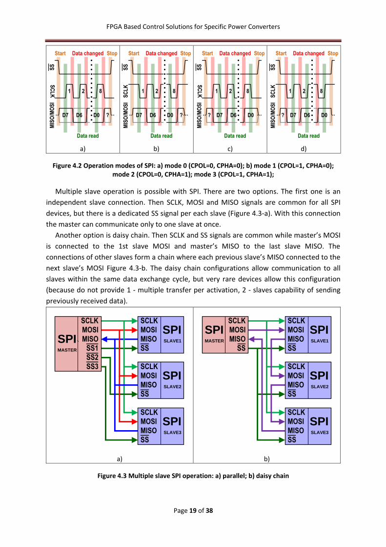
Multiple slave operation is possible with SPI. There are two options. The first one is an
independent slave connection. Then SCLK, MOSI and MISO signals are common for all SPI
devices, but there is a dedicated SS signal per each slave (Figure 4.3-a). With this connection
the master can communicate only to one slave at once.
Another option is daisy chain. Then SCLK and SS signals are common while master’s MOSI
is connected to the 1st slave MOSI and master’s MISO to the last slave MISO. The
connections of other slaves form a chain where each previous slave’s MISO connected to the
next slave’s MOSI Figure 4.3-b. The daisy chain configurations allow communication to all
slaves within the same data exchange cycle, but very rare devices allow this configuration
(because do not provide 1 - multiple transfer per activation, 2 - slaves capability of sending
previously received data).
SPISLAVE1
SCLK
MOSI
MISO
SSSPIMASTER
SCLK
MOSI
MISO
SS1
SS2
SS3
`
SPISLAVE2
SCLK
MOSI
MISO
SS
SPISLAVE3
SCLK
MOSI
MISO
SS
a)
SPISLAVE1
SCLK
MOSI
MISO
SS
SPISLAVE2
SCLK
MOSI
MISO
SS
SPISLAVE3
SCLK
MOSI
MISO
SS
SPIMASTER
SCLK
MOSI
MISO
SS
b)
Figure 4.3 Multiple slave SPI operation: a) parallel; b) daisy chain

FPGA Based Control Solutions for Specific Power Converters
Page 20 of 38
Communication of Programmable Logic and SPI
The simplest occasion of SPI communication is repetitive data exchange with continuous
(constant frequency) clock signal. It has the following features:
1) Scheme of communication can be regarded as “clock-slave-slave”, but not “master-slave”;
2) Both devices can be described as finite state machines (a synchronous digital system with
limited number of states which are toggled on changes of synchronisation signal – SPI clock
in the given case);
3) Programmable logic device can be easy configured from a VHDL script utilizing operator
“process”, but the digital entity may have standard logic signal corresponding to SPI
interface, an integer or real output V and an integer or real internal variable T to store
temporary result; an option is a standard logic output of communication error.
Below two examples of such operation/configuration are described.
Data read from ADCS7476
IC ADCS7476 is a monolithic single channel 12-bit ADC. It does not need any configuration
and, besides its clock SCLK and select CS=SS inputs, has only data output SDATA which is
equivalent of MISO (Figure 4.4-a). The use of this IC assumes that all modifications occur at
the falling edge, but readings – at the rising edge of SCLK which normally (in the idle mode)
has to be high (CPOL=1, CPHA=1, SPI mode 3). Taking into account that the number of data
bits is 12, number of zero-bits with no meaning is 3, but the minimal number of clock pulses
during the idle state is 1, as well as taking into account that there must a delay between the
chip select and first reading finally the data transmission cycle can occur in 17 periods of
SCLK signal. These intervals can be divided into 4 groups (Figure 4.5):
1) Idle interval in which CS is kept high (1), but the output signal V of the “process”
operator is rewritten from its internal temporary variable T;
2) Start interval when CS is set low (0);
AD
CS
74
76
VIN
CS
GND
VDD
SCLK
SDATA
a)
DGND
VDD
VREF
AGND
CH3
CH2
CH1
CH0
CS
DIN
CLK
DOUT
MC
P3
00
4
b)
Figure 4.4 Electrical connections of two analog-to-digital converters ISs: a) ADCS7476 with unidirectional data transfer; a) MCP3004 with bidirectional data transfer
FPGA Based Control Solutions for Specific Power Converters
Page 21 of 38
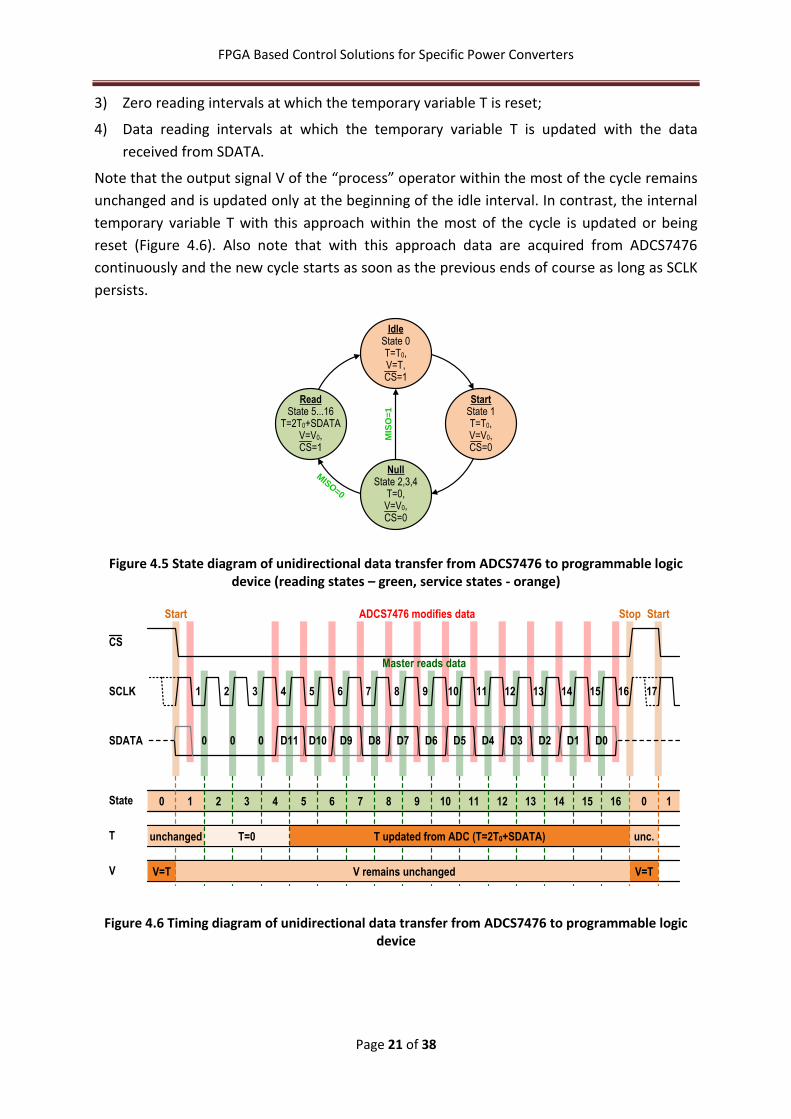
3) Zero reading intervals at which the temporary variable T is reset;
4) Data reading intervals at which the temporary variable T is updated with the data
received from SDATA.
Note that the output signal V of the “process” operator within the most of the cycle remains
unchanged and is updated only at the beginning of the idle interval. In contrast, the internal
temporary variable T with this approach within the most of the cycle is updated or being
reset (Figure 4.6). Also note that with this approach data are acquired from ADCS7476
continuously and the new cycle starts as soon as the previous ends of course as long as SCLK
persists.
Idle
State 0T=T0,V=T,CS=1
StartState 1T=T0,V=V0,CS=0
NullState 2,3,4
T=0,V=V0,CS=0
ReadState 5...16
T=2T0+SDATAV=V0,CS=1
MISO
=0
MIS
O=
1
Figure 4.5 State diagram of unidirectional data transfer from ADCS7476 to programmable logic device (reading states – green, service states - orange)
1
Start
SCLK
SDATA
CS
1 162 3 4 5 6 7 8 9 10 11 12 13 14 15
D11 D10 D9 D8 D7 D6 D5 D4 D3 D2 D1 D0
Start StopADCS7476 modifies data
000
Master reads data
State 1 2 3 4 5 6 7 8 9 10 11 12 13 14 15 16 00
17
V
T T updated from ADC (T=2T0+SDATA)T=0 unc.
V=TV=T
unchanged
V remains unchanged
Figure 4.6 Timing diagram of unidirectional data transfer from ADCS7476 to programmable logic device
FPGA Based Control Solutions for Specific Power Converters
Page 22 of 38
Device configuration and data read from MCP3004 (MCP3008)
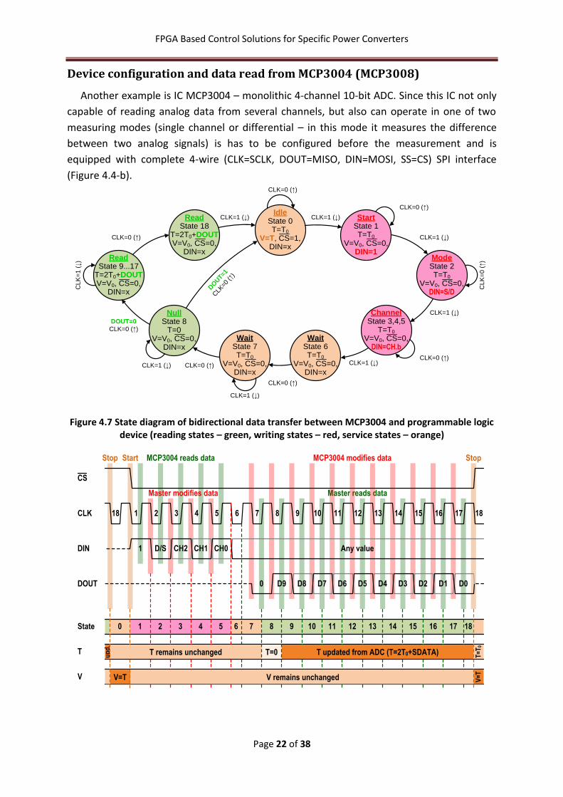
Another example is IC MCP3004 – monolithic 4-channel 10-bit ADC. Since this IC not only
capable of reading analog data from several channels, but also can operate in one of two
measuring modes (single channel or differential – in this mode it measures the difference
between two analog signals) is has to be configured before the measurement and is
equipped with complete 4-wire (CLK=SCLK, DOUT=MISO, DIN=MOSI, SS=CS) SPI interface
(Figure 4.4-b).
IdleState 0T=T0
V=T, CS=1,DIN=x
StartState 1T=T0
V=V0, CS=0,DIN=1
ReadState 18
T=2T0+DOUTV=V0, CS=0,
DIN=xRead
State 9...17T=2T0+DOUTV=V0, CS=0,
DIN=x
ModeState 2T=T0
V=V0, CS=0,DIN=S/D
NullState 8
T=0V=V0, CS=0,
DIN=x
ChannelState 3,4,5
T=T0
V=V0, CS=0,DIN=CH.b
WaitState 6T=T0
V=V0, CS=0,DIN=x
WaitState 7T=T0
V=V0, CS=0,DIN=x
CLK=0 (↑)
CLK=1 (↓)CLK=1 (↓)
CL
K=
0 (↑)
CLK=0 (↑)
CLK=1 (↓)
CLK=1 (↓)
CLK=1 (↓)
CLK=0 (↑)
DOUT=0
CLK=0 (↑)
CLK=0 (↑)
CLK=0 (↑)
CLK=0 (↑)
CLK=1 (↓)
DO
UT=1
CLK
=0 (↑
)
CLK=1 (↓)
CL
K=
1 (↓)
Figure 4.7 State diagram of bidirectional data transfer between MCP3004 and programmable logic device (reading states – green, writing states – red, service states – orange)
Stop MCP3004 reads data
Master reads data
MCP3004 modifies data
Master modifies data
CLK
DOUT
CS
1 162 3 4 5 6 7 8 9 10 11 12 13 14 15
D9 D8 D7 D6 D5 D4 D3 D2 D1 D0
Start Stop
0
DIN CH0CH1CH21 Any valueD/S
17
State 1 2 3 4 5 6 7 8 9 10 11 12 13 14 15 16 180
1818
17
V
T T=0
V=T V remains unchanged V=
TT
=T
0
T updated from ADC (T=2T0+SDATA)up
d.
T remains unchanged

FPGA Based Control Solutions for Specific Power Converters
Page 23 of 38
Figure 4.8 Timing diagram of bidirectional data transfer between MCP3004 and programmable logic device
Operation cycle remains similar because it is also a mode 3 SPI device (CPOL=1, CPHA=1) –
so that readings occur at the rising edge, but writings – at the falling. Although the number
of data bits (10 as against 12) and null bits (1/3) is lower the total number of time intervals in
the data exchange cycle is almost the same (19/17). Nevertheless new types of these
intervals make the corresponding state diagram more complicated (Figure 4.7). Now it
includes the following types of intervals and states:
1) Idle interval (S0) in which CS is kept high (1), the output signal V is rewritten from the
temporary variable T; So this interval remains similar like in the previous example;
2) The start interval (S1) now together with CS=0 sets also DIN=1 indicating the start of
data writing into MCP3004;
3) In the next interval (S2) the measuring mode is programmed by setting DIN=0 for single
channel measurements or DIN=1 for differential measurements;
4) In the following 3 intervals (S3…S5) the channel is chosen by programming DIN with the
appropriate value; For example DIN is always 0 if the data have to be acquired from the
channel 0; Interval S3 is useful with MCP3008 which has 8 channels and needs 3 bits of
address;
5) Note that the intervals S1…S5 starts and ends at the falling edge of the CLK that
corresponds to writings; At the same time the next intervals are reading intervals that
starts and ends at the rising edge; For this reason in the cycle appears waiting interval S6
that starts at the falling edge of CLK, ends at its rising edge and lasts for a half of a
period of CLK;
6) The next waiting interval S7 is complete; It starts and ends at the rising edge of CLK;
7) As soon as the IC is configured and after some delay the data can be read from the IC;
However, the first bit read from the IC (state S8) is not a valuable bit and has to be 0; if it
is 0 the temporary variable T is reset and is ready to receive data;
8) S9…S17 are the data reading intervals at which the temporary variable is updated with
the data received from DOUT;
9) So the S18 is also data reading and variable T updating interval; However, this interval
only starts at the rising edge of CLK, but ends – at the falling and lasts one half of the CLK
period; This, second (the first is S6), “half” interval is necessary to keep continuity of the
clock and to make the complete length of the data exchange cycle equal to integer
number of CLK periods (19).
Note that, like in the previous example, the output signal V of the “process” operator the
most of the cycle remains unchanged and is updated only in the idle interval (S0). The
internal temporary variable T in this example is kept unchanged while the master configures
the IC. Then it is reset and updated (Figure 4.8). Also note that, like in the previous example,
data are acquired from IC continuously and the new cycle starts as soon as the previous ends.
FPGA Based Control Solutions for Specific Power Converters
Page 24 of 38
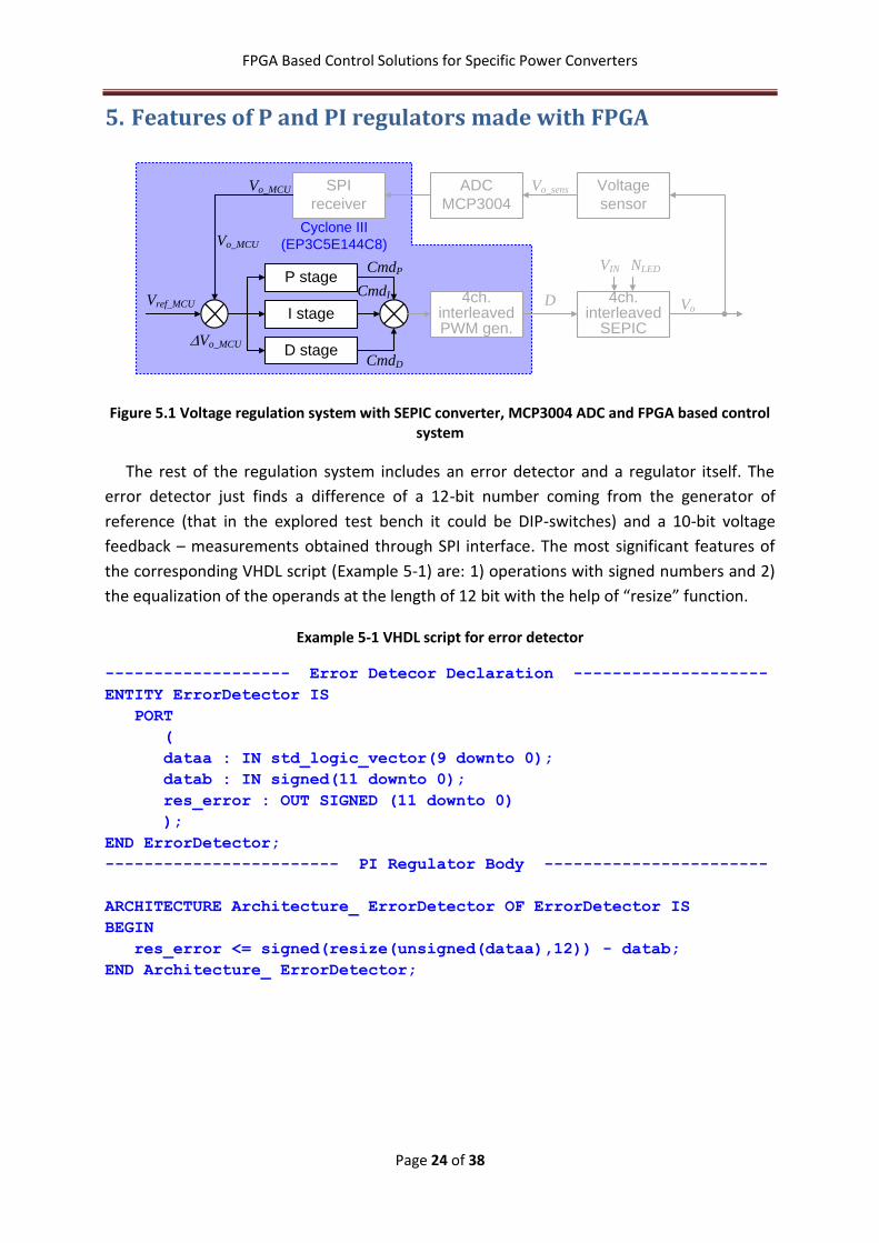
5. Features of P and PI regulators made with FPGA
D4ch. interleaved PWM gen.
Voltage
sensor
ADC
MCP3004
Vo_sens
CmdP VIN
4ch. interleaved
SEPIC
NLED
Vo
SPI
receiver
P stage
Vref_MCU
Vo_MCU
DVo_MCU
Vo_MCU
Cyclone III
(EP3C5E144C8)
I stage
D stageCmdD
CmdI
Figure 5.1 Voltage regulation system with SEPIC converter, MCP3004 ADC and FPGA based control system
The rest of the regulation system includes an error detector and a regulator itself. The
error detector just finds a difference of a 12-bit number coming from the generator of
reference (that in the explored test bench it could be DIP-switches) and a 10-bit voltage
feedback – measurements obtained through SPI interface. The most significant features of
the corresponding VHDL script (Example 5-1) are: 1) operations with signed numbers and 2)
the equalization of the operands at the length of 12 bit with the help of “resize” function.
Example 5-1 VHDL script for error detector
------------------- Error Detecor Declaration --------------------
ENTITY ErrorDetector IS
PORT
(
dataa : IN std_logic_vector(9 downto 0);
datab : IN signed(11 downto 0);
res_error : OUT SIGNED (11 downto 0)
);
END ErrorDetector;
------------------------ PI Regulator Body -----------------------
ARCHITECTURE Architecture_ ErrorDetector OF ErrorDetector IS
BEGIN
res_error <= signed(resize(unsigned(dataa),12)) - datab;
END Architecture_ ErrorDetector;

FPGA Based Control Solutions for Specific Power Converters
Page 25 of 38
The last, but not the least part of the regulation system is a regulator with the function
providing the control command based on the calculated error.
DIP CMDCMDCMDCMD , (3.3)
where
oPP ΔVKCMD , (3.4)
t
0
o
I
I dtΔVT
1CMD and (3.5)
dt
VdΔTCMD oDD . (3.6)
In (3.4), (3.5) and (3.6) KP – is the proportional gain which expresses the direct amplification
rate of the calculated reference and feedback error ∆VO, TI – is the integration period in
which the command coming through the integral stage is becoming equal to those of
proportional stage (without taking into account KP) and TD is differential time constant.
The most popular regulator is proportionally-integral. In practice such regulators are
designed based on digital technique. Then the integral becomes a sum of time steps and the
values of the error. Then the finite differences equation for PI regulator after M
measurements is the following:
M
1k
kOk
I
ONP ΔtΔVT
1ΔVKCMD . (3.7)
If ∆t is constant (3.7) can be rewritten as
M
1k
Ok
I
ONP ΔVN
1ΔVKCMD . (3.8)
(3.8) is a practical formula usable in real calculations. A version of its realization with VHDL is
given below as Example 5-2.
Example 5-2 VHDL Script for PI regulator
-------------------- PI Regulator Declaration --------------------
ENTITY PI IS
generic
(
DATA_WIDTH : natural := 12
);
port
(
input : in signed ((DATA_WIDTH-1) downto 0);
clk : in std_logic;
reset : in std_logic;
output : out signed ((2*DATA_WIDTH-1) downto 0)
);
END PI;

FPGA Based Control Solutions for Specific Power Converters
Page 26 of 38
------------------------ PI Regulator Body -----------------------
ARCHITECTURE PI_architecture OF PI IS
signal sum : signed ((2*DATA_WIDTH-1) downto 0);
signal old_sum : signed ((2*DATA_WIDTH-1) downto 0);
signal out_reg : signed ((2*DATA_WIDTH-1) downto 0);
signal in_reg : signed ((DATA_WIDTH-1) downto 0);
constant TIME_CONSTANT : signed ((DATA_WIDTH-1) downto 0)
:= "000000001000";
constant P : signed ((DATA_WIDTH-1) downto 0)
:= "000000001000";
BEGIN
process (sum)
begin
old_sum <= sum;
end process;
process (clk)
begin
if (rising_edge(clk)) then
if reset = '1' then
sum <="000000000000000000000000";
else
in_reg <= input;
sum <= old_sum +"000000000001"*in_reg/TIME_CONSTANT;
out_reg <= in_reg/P + sum;
end if;
end if;
end process;
output<=out_reg;
END PI_architecture;

FPGA Based Control Solutions for Specific Power Converters
Page 27 of 38
Appendix A: VHDL Quick Reference
Based on [5] and [6].
1. Basic Definitions
VHDL is not case sensitive that can be used for formatting. VHDL constructions are hardly
defined by its lexical elements. That is why lines can be of any length, but long constructions
can occupy few lines. The most of the constructions end with semicolon “;”. Comments start
with “--“ and are valid till the end of the line.
VHDL script often starts from a library and package declaration
library <LIBRARY_NAME>;
use <LIBRARY_NAME>.<PACKAGE_NAME>.<MODULE_NAME>;
Frequently used:
library ieee;
and
use ieee.std_logic_1164.all;
use ieee.std_logic_unsigned.all;
use ieee.std_logic_arith.all;
use ieee.numeric_std.all;
VHDL script must contain declaration and description of at least one digital entity. The entity
is declared as
entity <NAME_OF_ENTITY> is
[generic (
<CONSTANT_NAME1>: <TYPE1> [:=<VALUE1>] ;
...
<CONSTANT_NAMEn>: <TYPEn> [:=<VALUEn>] );]
port (
<PORT_NAMES1>: <MODE1> <TYPE1>;
...
<PORT_NAMESn>: <MODEn> <TYPEn>);
end [<NAME_OF_ENTITY>];
The description of the entity is declared as
architecture <ARCHITECTURE_NAME> of <NAME_OF_ENTITY> is
-- declarations
begin
-- concurrent statements (describes the design)
end [architecture] <ARCHITECTURE_NAME>;
where “declarations” are given as in section 4, but concurrent statements as in section 6.
2. Operators
Logical operators:
and, or, xor, nand, nor, xnor

FPGA Based Control Solutions for Specific Power Converters
Page 28 of 38
Relational operators:
=, /=, <, <=, >, >=
Shift left/right logical operators (vacated bits filled with zeros):
sll, srl
Shift left/right arithmetic operators (vacated bits stay with previous values):
sla, sra
Rotate left/right operators (vacated bits filled with exiting bits):
rol, ror
Arithmetical operators:
+, -, *, /, **
Concatenation operator (‘111’&’000’=’111000’):
&
Reminder operator (10 rem 3 = 1):
rem
Division modulo operator (7 mod 4 = 3; -7 mod -4 = -3; 7 mod -4 = -1)
mod
3. Frequently Used Data Types
Type Values
bit ‘0’ and ‘1’
bit_vector array of ‘0’ and ‘1’
std_ulogic
std_logic
‘U’ (uninitialized), ‘X’ (forcing unknown), ‘0’
(forcing 0), ‘1’ (forcing 1), ‘Z’ (high
impedance), ‘W’ (weak unknown), ‘L’ (weak 0), ‘H’
(weak 1), as well as ‘-‘ (don’t care)
(in std_logic_1164 package)
std_ulogic_vector
std_logic_vector
array of std_ulogic
(in std_logic_1164 package)
Boolean TRUE, FALSE
character 7-bit ASCII
string array of characters
integer signed 32 bit at least
natural integer ≥ 0
positive integer > 0
real floating point 32 bit, +1e38...-1e38
4. Declarations
7.1 Declaration of scalar data types
type <TYPE_IDENTIFIER> is range <MIN> to <MAX>;
type <TYPE_IDENTIFIER> is range <MAX> downto <MIN>;
type <TYPE_IDENTIFIER> is (<list_of_values>);
for example
type SMALL_INT is range 0 to 1024;
type MY_WORD_LENGTH is range 31 downto 0;

FPGA Based Control Solutions for Specific Power Converters
Page 29 of 38
type MY_VALUES is (‘0’, ‘1’, ‘Z’);
7.2 Declaration of array data types
type <ARRAY_ID> is array (<indexing scheme>) of <TYPE_ID>;
for example
type WORD16A is array (15 downto 0) of std_logic;
type WORD16D is array (0 to 15) of std_logic;
7.3 Declaration of constants
constant <LIST_OF_NAMES_OF_CONSTANT>: <type> [:= <INITIAL_VALUE>];
for example
constant PERIOD: time := 10 us;
constant MD_BUS, MA_BUS: integer:= 16;
7.4 Declaration of variables
variable <LIST_OF_VARIABLES>: type [:= <INITIAL_VALUE>];
for example
variable VAR_BIT: bit :=0;
variable VAR_BOOLEAN: boolean :=FALSE;
variable VAR_INTEGER: integer :=1000;
variable CNTR: integer range 0 to 15;
variable VAR_BIT_V: bit_vector (3 downto 0);
7.5 Declaration of signals
signal <LIST_OF_SIGNALS>: <type> [ := <INITIAL_VALUE>] ;
for example
signal A_NOT, A_NOT, INT_1, INT_2: std_logic;
signal MY_VALUE: integer :=0;
signal CNTR: integer range 0 to 15;
signal MD_BUS: bit_vector (0 to 15);
7.6 Declaration of components – digital entities described in the same file
component <COMPONENT_NAME> [is]
[port (<port_name_1>: mode <type>;
<port_name_2>: mode <type>;
...
<port_name_N>: mode <type>);]
end component [<COMPONENT_NAME>];
for example

FPGA Based Control Solutions for Specific Power Converters
Page 30 of 38
component AND3
port (IN1, IN2, IN3: in std_logic;
OUTx: out std_logic);
end component;
5. Some Attributes
Length of array (an integer value)
<ARRAY_ID>‘length
Signal delayed by T (also a signal)
<SIGNAL_ID>‘delayed(T)
Value of driver (also a signal)
<SIGNAL_ID>‘driving_value
Event (rising or falling edge) detector (TRUE or FALSE)
<SIGNAL_ID>‘event
6. Statements
9.1 Concurrent statements
Statement “process”
[<PROCESS_LABEL>:] process [<sensitivity_list>] [is]
[<process_declarations>]
begin
<list of sequential statements such as:
signal assignments
variable assignments
case statement
exit statement
if statement
loop statement
next statement
null statement
procedure call
wait statement>
end process [<PROCESS_LABEL>];
for example
process(EnableSignal, DataWord)
begin
if (EnableSignal = '1') then
LatchVariable <= DataWord;
end if;
end process;
Instance of component
FPGA Based Control Solutions for Specific Power Converters
Page 31 of 38
<INSTANCE_NAME> : <COMPONENT_NAME>
port map (<signal_name_1> , ..., <signal_name_N>);
Example of component with explicit signal assignment
DD1: AND3 port map (OUTx=>Prod, IN1=>InA, IN2=>InB, IN1=>InvInA)
Example of component with implicit signal assignment
DD1: AND3 port map (InA, InB, InvInA, Prod)
Unconditional concurrent signal assignments
<TARGET_SIGNAL> <= <expression> [after <delay>];
For example
MySignal <= ‘1’;
MySignal <= ‘1’ after 10ns;
Conditional concurrent signal assignments
<TARGET_SIGNAL> <=
<EXPRESSION1> when <CONDITION1> else
<EXPRESSION2> when <CONDITION2> else
...
<EXPRESSIONn>;
For example
Q <=
A when SEL=”00” else
B when SEL=”01” else
C when SEL=”10” else
D when SEL=”11” else
‘X’;
Selective concurrent signal assignments
with <CHOICE_EXPRESSION> select
<TARGET_SIGNAL> <=
<EXPRESSION1> when <CHOICE1>,
<EXPRESSION2> when <CHOICE2>,
...
[<EXPRESSIONn> when others];
For example
with SEL select
Q <=
A when “00”,
B when “01”,
C when “10”,
D when “11”,
‘X’ when others;
FPGA Based Control Solutions for Specific Power Converters
Page 32 of 38
9.2 Sequential statements
Waiting statement
wait until <CONDITION>;
wait for <TIME >;
wait on <SIGNAL1> [,<SIGNAL2> ...];
wait;
for example
wait until CNTR=10;
wait until CLK=’0’;
wait until CLK’EVENT and CLK=’0’;
wait until CLK’STABLE(10ms) and CLK=’1’;
wait for 1s
Conditional statement
if <condition 1> then <sequential statements 1...
...>
[elsif <condition k> then <sequential statements k...
...>]
[else <sequential statements N>]
end if;
for example
if (CLEAR = ‘1’) then
INT_Q := ‘0’;
elsif (CLK’EVENT and CLK = ‘1’) then
INT_Q := D;
end if;
Choice statement
case <expression> is
when <choice 1> => <sequential statements 1>
...
when <choice k> => <sequential statements k>
...
[when others => <sequential statements N>]
end case;
for example
case SEL is
when “00” => TMP := A;
when “01” => TMP := B;
when “10” => TMP := C;
when “11” => TMP := D;
when others => TMP := ‘X’;
end case;
FPGA Based Control Solutions for Specific Power Converters
Page 33 of 38
Conditional loop statement
[<LOOP_LABEL>:] while <condition> loop
-- sequential statements
[next [<LOOP_LABEL>] [when <condition_n>];
[exit [<LOOP_LABEL>] [when <condition_e>];
end loop [<LOOP_LABEL>];
for example
while ( LoopVar < 21 ) loop
Sum:=Sum+LoopVar;
LoopVar:=LoopVar+1;
End loop ;
Counted loop statement
[<LOOP_LABEL>:] for <IDENTIFIER> in <range> loop
-- sequential statements
[next [<LOOP_LABEL>] [when <condition_n>];
[exit [<LOOP_LABEL>] [when <condition_e>];
end loop [<LOOP_LABEL>];
for example
for LoopVar in (0 to 20) loop
Sum:=Sum+LoopVar;
end loop;
FPGA Based Control Solutions for Specific Power Converters
Page 34 of 38
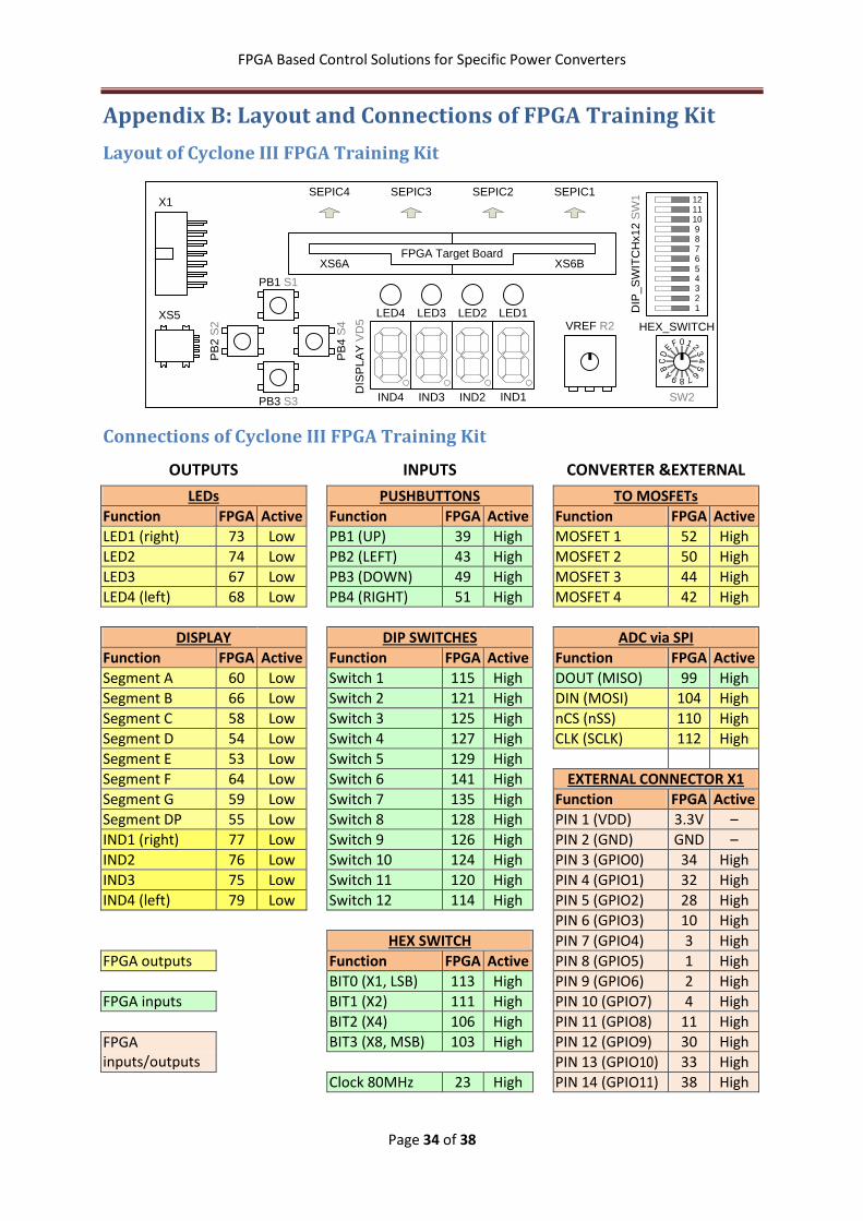
Appendix B: Layout and Connections of FPGA Training Kit
Layout of Cyclone III FPGA Training Kit
FPGA Target BoardXS6A XS6B
SEPIC1SEPIC2SEPIC3SEPIC4
0FE
DC
B
A 9 8 7
6
54
3
21
X1
XS5 LED1LED3 LED2LED4
IND1IND3 IND2IND4
DIS
PL
AY
VD
5
DIP
_S
WIT
CH
x1
2 S
W1
67
5
111098
1234
12
VREF R2
SW2
HEX_SWITCH
PB1 S1
PB
2 S
2
PB3 S3
PB
4 S
4
Connections of Cyclone III FPGA Training Kit
OUTPUTS INPUTS CONVERTER &EXTERNAL
LEDs PUSHBUTTONS TO MOSFETs
Function FPGA Active Function FPGA Active Function FPGA Active
LED1 (right) 73 Low PB1 (UP) 39 High MOSFET 1 52 High
LED2 74 Low PB2 (LEFT) 43 High MOSFET 2 50 High
LED3 67 Low PB3 (DOWN) 49 High MOSFET 3 44 High
LED4 (left) 68 Low PB4 (RIGHT) 51 High MOSFET 4 42 High
DISPLAY DIP SWITCHES ADC via SPI
Function FPGA Active Function FPGA Active Function FPGA Active
Segment A 60 Low Switch 1 115 High DOUT (MISO) 99 High
Segment B 66 Low Switch 2 121 High DIN (MOSI) 104 High
Segment C 58 Low Switch 3 125 High nCS (nSS) 110 High
Segment D 54 Low Switch 4 127 High CLK (SCLK) 112 High
Segment E 53 Low Switch 5 129 High
Segment F 64 Low Switch 6 141 High EXTERNAL CONNECTOR X1
Segment G 59 Low Switch 7 135 High Function FPGA Active
Segment DP 55 Low Switch 8 128 High PIN 1 (VDD) 3.3V –
IND1 (right) 77 Low Switch 9 126 High PIN 2 (GND) GND –
IND2 76 Low Switch 10 124 High PIN 3 (GPIO0) 34 High
IND3 75 Low Switch 11 120 High PIN 4 (GPIO1) 32 High
IND4 (left) 79 Low Switch 12 114 High PIN 5 (GPIO2) 28 High
PIN 6 (GPIO3) 10 High
HEX SWITCH PIN 7 (GPIO4) 3 High
FPGA outputs Function FPGA Active PIN 8 (GPIO5) 1 High
BIT0 (X1, LSB) 113 High PIN 9 (GPIO6) 2 High
FPGA inputs BIT1 (X2) 111 High PIN 10 (GPIO7) 4 High
BIT2 (X4) 106 High PIN 11 (GPIO8) 11 High
FPGA inputs/outputs
BIT3 (X8, MSB) 103 High PIN 12 (GPIO9) 30 High
PIN 13 (GPIO10) 33 High
Clock 80MHz 23 High PIN 14 (GPIO11) 38 High

FPGA Based Control Solutions for Specific Power Converters
Page 35 of 38
Appendix C: Schematics of FPGA Training Kit
Main Board
LE
D_4
R2
21
00
R
IND
_E
AC
P_
MO
SI
R4
03
90
R
IND
_2
EX
T_
3
R2
10
k
C1
41
00
nF
IND
_4
IND
_2
PW
M_4
C1
47
uF
-25
V
DIP
_4
XS
3
PELS_MODULE
65
3 4
21
VoutGND
Ctr
lG
ND
GNDVin
EX
T_7
C1
6
10
0n
F
C2
21
00
nF
Ctr
l1
R2
41
00
R
LE
D_3
AC
P_C
LK
C9
22
uF
PW
M_1
EX
T_
9
R4
63
90
R
IND
_G
PW
M_3
R3
31
00
R
EX
T_
8
U1
1
MC
P1
40
2
1234 5
GN
DV
cc
ING
ND
OU
T
EX
T_8
C5
10
0n
F
R2
81
00R
IND
_D
R5
9
R0
12
5K
01
0_X
6/7
P1
234567
EX
T_
4
AC
P_n
CS
D2PMEG2015EPK
IND
_A
DIP
_3
R1
81
00
R
IND
_G
PW
M_2
L1
2u
2H
EX
T_1
0
R1
0R
1
DIP
_0
U9
SI8
44
11 2 3 4 5 6 7 8
910
11
12
13
14
15
16
VD
D1
GN
D1
IN_
1IN
_2
IN_
3O
UT
_4
EN
1G
ND
1G
ND
2E
N2
IN_4
OU
T_3
OU
T_2
OU
T_1
GN
D2
VD
D2
C2
01
00n
F
DIP
_7
VD
3L
ED
nC
S
LE
D_4
R4
33
90
R
HE
X_3
PB
_1
R1
52
2k
DIP
_2
PW
M_1
R1
4
1k
PW
M_3
R7100k
EX
T_3
R2
11
00
R
C1
21
00n
F
HE
X_0
R5
01
0k
Q2
PN
P C
EB
EX
T_
6
MIS
O
J2 CO
N2
1 2
LE
D_2
EX
T_0
C8100nF
DIP
_1
0
nC
S
C2
11
00n
F
EX
T_
2
R3
01
00
R
DIP
_4
U1
2
MC
P1
40
2
1234 5
GN
DV
cc
ING
ND
OU
T
R1
3
15
PB
_4
C1
01
00
nF
DIP
_5
PB
_3
SW
2
SW
DIP
-HE
X
32
6 145
4C
8 12C
Ctr
l3
EX
T_
0
XS
4
PELS_MODULE
65
3 4
21
VoutGND
Ctr
lG
ND
GNDVin
A_V
ou
t
CL
K
VD
2L
ED
DIP
_1
R4
53
90
R
DIP
_3
R3
11
00
R
C1
8
10
0n
F
IND
_A
R2
31
00
R
IND
_B
PB
_2
C
R51
R0125K010_X4/5P
1
2345
IND
_1
PB
_1
XS
1
PELS_MODULE
65
3 4
21
VoutGND
Ctr
lG
ND
GNDVin
Vin
MO
SI
R4
23
90
R
DIP
_9
C2
8
22
uF
EX
T_4
R2
51
00
R
U1
0
MC
P1
40
2
1234 5
GN
DV
cc
ING
ND
OU
T
HE
X_2
Q1
PN
P C
EB
R5
31
k
A_
Vin
DIP
_1
0Q
3P
NP
CE
B
DIP
_1
HE
X_0
R1
91
00
R
IND
_3
MIS
O
C1
9
10
0n
FD
IP_6
R5733K
Vin
U6
MC
P1
40
2
1234 5
GN
DV
cc
ING
ND
OU
TR
29
10
0R
PB
_3
R2
61
00R
PB
_4
DIP
_8
R4
13
90
R
DIP
_9
HE
X_1
R31k
IND
_4
Vre
fC
11
10
0n
F
DIP
_1
1
C6
10
0n
F
Vin
R4
71
0k
XS
2
PELS_MODULE
65
3 4
21
VoutGND
Ctr
lG
ND
GNDVin
EX
T_9
Q4
PN
P C
EB
DIP
_6
S2
IND
_F
HE
X_2
R9
45
k
LE
D_1
A_
Iou
t
R4
43
90
R
EX
T_
1
C1
7
10
0n
F
D3
LM4041
Vin
R3
21
00
R
R1
21
0k
EX
T_1
C3
4
10
0n
F HE
X_1
R1
61
k
IND
_D
P
HE
X_3
R3
71
k
PW
M_2
A_V
in
U7
LM
R1
05
10
5 4
1
2
3
Vin
EN
SW
GND
FB
DIP
_5
VD
4L
ED
LE
D_3
Vin
VD
1L
ED
R3
93
90
R
EX
T_1
0
C2
220uF-63V
IND
_C
R3
61
k
Vre
f
R3
41
00
R
LE
D_1
Vre
f
S1
R56100R
DIP
_0
S4
CL
K
Ctr
l4
R2
01
00
R
XS
6A
FP
GA
_C
3_
CB
78
91
01
11
21
31
41
51
61
71
81
92
02
12
22
32
42
52
62
72
82
93
03
13
23
33
43
53
63
73
83
94
0
12
34
56
P_
00
1P
_0
02
P_
00
3P
_0
04
P_
01
0P
_0
11
P_
02
8P
_0
30
P_
03
2P
_0
33
P_
03
4P
_0
38
P_
03
9P
_0
42
P_
04
3P
_0
44
P_
04
9P
_0
50
P_
05
1P
_0
52
P_
05
3P
_0
54
P_
05
5P
_0
58
P_
05
9P
_0
60
P_
06
4P
_0
66
P_
06
7P
_0
68
A1
A2
A3
A4
KE
YK
EY
Vd
dV
dd
GN
DG
ND
EX
T_2
U8
SI8
44
01 2 3 4 5 6 7 8
910
11
12
13
14
15
16
VD
D1
GN
D1
IN_
1IN
_2
IN_
3IN
_4
NC
GN
D1
GN
D2
EN
2O
UT
_4
OU
T_3
OU
T_2
OU
T_1
GN
D2
VD
D2
IND
_C
U5 NX
11
17
C
32 4
1
Vin
Vo
ut
Vo
ut
AD
J/G
ND
LE
D_2
C3
10
0n
F
Ctr
l2
A_V
ou
t
XS
6B
FP
GA
_C
3_
CB
41
42
43
44
45
46
47
48
49
50
51
52
53
54
55
56
57
58
59
60
61
62
63
64
65
66
67
68
69
70
71
72
73
74
75
76
77
78
79
80
Vd
dV
dd
GN
DG
ND
P_0
74
P_0
73
P_0
76
P_0
75
P_0
79
P_0
77
P_0
84
P_0
83
P_0
86
P_0
85
P_0
98
P_0
87
P_1
00
P_0
99
P_1
03
P_1
01
P_1
06
P_1
04
P_1
11
P_1
10
P_1
13
P_1
12
P_1
15
P_1
14
P_1
21
P_1
20
P_1
25
P_1
24
P_1
27
P_1
26
P_1
29
P_1
28
P_1
41
P_1
35
GN
DG
ND
PB
_2
on
1SW
1
SW
DIP
-12
IND
_D
Ctr
l3
C1
31
00n
F
X1
ML
14
1 2 3 4 5 6 7 8 9 10
11
12
13
14
EX
T_1
1
XS
5
Min
iUS
B_
B
1 2 35 B1
B2
B3
B4
US
B_5
V
D-
D+
US
B_
GN
D
Sh
ield
Sh
ield
Sh
ield
Sh
ield
IND
_D
P
R5
41
k
MO
SI
R2
71
00R
DIP
_8
AC
P_
MIS
O
R5
21
k
DIP
_1
1
DIP
_2
R4
81
0k
EX
T_
5
IND
_B
Ctr
l2
R5
51
k
DIP
_7
C7
10
0n
F
EX
T_5
R3
5 1k
IND
_F
U4 ZX
CT
10
51
1 2 345
Vcc
GN
DO
ut
Vs+
Vs-
R5
8R
01
25
K0
10_
X6/7
P
1
234567
C4
10
0n
F
EX
T_
7
U3
MC
P3
00
4
1413 12
1 2 3 4 56
7
891
01
1
VddVref Agnd
CH
1C
H2
CH
3C
H4
nc
nc
Dgnd
CS
Din
Do
ut
CL
K
IND
_E
A_Io
ut
J4 CO
N3
1 2 3
IND
_1
EX
T_1
1
R3
8 1k
Ctr
l4
Ctr
l1
VD
5C
A5
6-1
2
12 9
10
5 311
7 4 2 18 6
C1
C2
F GD
PA B C D EC
3
C4
PW
M_4
C3
3
22
uF
EX
T_6
S3
IND
_3R
49
10
k

FPGA Based Control Solutions for Specific Power Converters
Page 36 of 38
FPGA Cyclone III Target Board
PIN
05
5
PIN
05
3
PIN
11
4
U6
NX
11
17
CE
12
Z
32 4 1
Vin
Vo
ut
Vo
ut
AD
J/G
ND
PIN
07
2
PIN
03
2
PIN
10
3
C3
3
22
uF
PIN
12
0
AI1
D1
LE
D
PIN
05
2
PIN
10
6
PIN
00
2
C2
41
00
nF
PIN
06
6
PIN
12
0
PIN
07
1
U1
B
AL
TE
RA
EP
3C
5E
14
4
Ve
rsio
n =
1.1
1 2 3 4 81
01
1
32
33
28
30
34
38
39
42
43
44
49
50
51
52
53
66
67
54
55
58
59
60
64
68
69
70
71
72
76
77
73
74
75
79
83
84
85
86
87
98
99
10
01
01
10
31
04
10
6
11
41
15
11
01
11
11
21
13
12
01
21
12
41
25
12
61
27
12
81
29
13
51
41
14
21
43
14
4
IO_
VB
1N
0_
1IO
_V
B1
N0
_2
IO_
VB
1N
0_
3IO
_V
B1
N0
_4
IO_
VB
1N
0_
8/D
IFF
IO_
L2
p/F
LA
SH
_n
CE
/nC
SO
IO_
VB
1N
0_
10
/DIF
FIO
_L
4p
/DQ
S0
L/C
Q1
L/D
PC
LK
0IO
_V
B1
N0
_1
1/D
IFF
IO_
L4
n
RU
P1
RD
N1
IO_
VB
2N
0_
28
/DIF
FIO
_L
6n
IO_
VB
2N
0_
30
/DIF
FIO
_L
8p
/DQ
S1
L/C
Q1
L#
/DP
CL
K1
IO_
VB
2N
0_
34
IO_
VB
3N
0_
38
/DIF
FIO
_B
1p
IO_
VB
3N
0_
39
/DIF
FIO
_B
1n
IO_
VB
3N
0_
42
IO_
VB
3N
0_
43
/PL
L1
_C
LK
OU
Tp
IO_
VB
3N
0_
44
/PL
L1
_C
LK
OU
Tn
IO_
VB
3N
0_
49
/DIF
FIO
_B
9p
IO_
VB
3N
0_
50
/DIF
FIO
_B
9n
IO_
VB
3N
0_
51
/DIF
FIO
_B
10
pIO
_V
B3
N0
_5
2/D
IFF
IO_
B1
1p
IO_
VB
3N
0_
53
/DIF
FIO
_B
11
n
RU
P2
RD
N2
IO_
VB
4N
0_
54
/DIF
FIO
_B
12
pIO
_V
B4
N0
_5
5/D
IFF
IO_
B1
2n
IO_
VB
4N
0_
58
/DIF
FIO
_B
15
pIO
_V
B4
N0
_5
9/D
IFF
IO_
B1
6p
IO_
VB
4N
0_
60
/DIF
FIO
_B
16
nIO
_V
B4
N0
_6
4IO
_V
B4
N0
_6
8/D
IFF
IO_
B2
0n/
DQ
S0
B/C
Q1
B/D
PC
LK
3IO
_V
B4
N0
_6
9IO
_V
B4
N0
_7
0/D
IFF
IO_
B2
1p
IO_
VB
4N
0_
71
/DIF
FIO
_B
21
nIO
_V
B4
N0
_7
2/D
IFF
IO_
B2
2p
RU
P3
RD
N3
IO_
VB
5N
0_
73
IO_
VB
5N
0_
74
IO_
VB
5N
0_
75
IO_
VB
5N
0_
79
/DIF
FIO
_R
10
nIO
_V
B5
N0
_8
3IO
_V
B5
N0
_8
4/D
IFF
IO_
R8
nIO
_V
B5
N0
_8
5/D
IFF
IO_
R8
p/D
QS
1R
/CQ
1R
#/D
PC
LK
4D
IFF
IO_
R7
nD
IFF
IO_
R7
p
DIF
FIO
_R
4n
DIF
FIO
_R
4p
IO_
VB
6N
0_
10
0IO
_V
B6
N0
_1
01
/DIF
FIO
_R
3n/
nCE
OD
IFF
IO_
R3
pIO
_V
B6
N0
_1
04
IO_
VB
6N
0_
10
6/D
IFF
IO_
R1
n/D
QS
2R
/CQ
3R
RU
P4
RD
N4
IO_
VB
7N
0_
11
0/D
IFF
IO_
T2
0p
/DQ
S0
T/C
Q1
T/D
PC
LK
6IO
_V
B7
N0
_1
11
/DIF
FIO
_T
19
pIO
_V
B7
N0
_1
12
/PL
L2
_C
LK
OU
Tn
IO_
VB
7N
0_
11
3/P
LL
2_
CL
KO
UT
pIO
_V
B7
N0
_1
20
/DIF
FIO
_T
16
nIO
_V
B7
N0
_1
21
/DIF
FIO
_T
16
p/D
QS
2T
/CQ
3T
IO_
VB
7N
0_
12
4/D
IFF
IO_
T1
3p
IO_
VB
7N
0_
12
5IO
_V
B7
N0
_1
26
/DIF
FIO
_T
12
nIO
_V
B7
N0
_1
27
/DIF
FIO
_T
12
p
IO_
VB
8N
0_
12
8/D
IFF
IO_
T1
1n
IO_
VB
8N
0_
12
9/D
IFF
IO_
T1
1p
IO_
VB
8N
0_
13
5/D
IFF
IO_
T8
nIO
_V
B8
N0
_1
41
/DIF
FIO
_T
5p
IO_
VB
8N
0_
14
2/D
IFF
IO_
T2
p/D
QS
1T
/CQ
1T
#/D
PC
LK
7IO
_V
B8
N0
_1
43
/DIF
FIO
_T
1n
IO_
VB
8N
0_
14
4/D
IFF
IO_
T1
p
PIN
01
0
PIN
12
7
C5
10
0n
F
PIN
12
4
AI2
PIN
03
8
R2
10
k
PIN
08
6
PIN
06
7
D2
PMEG2015EPK
PIN
06
7
PIN
13
5
C2
32
2u
F
PIN
06
6
PIN
03
3
PIN
10
6
Q1
SP
XO
00
94
41
42
13
Vc
cG
ND
EN
OU
T
PIN
10
0
AI3
C9
10
0n
F
PIN
01
0
PIN
07
7
R6
10
k
PIN
05
9
R1
27
R
PIN
05
4
PIN
09
9
PIN
00
3
C2222uF
PIN
03
4
PIN
10
0
PIN
08
5
AI4
Vint
PIN
05
4
R1
21
0k
PIN
11
0
PIN
03
9
PIN
05
5
PIN
10
1
C3
6
10
0n
F
AI1
PIN
02
8
PIN
12
9
R1
01
0k
PIN
12
8
Vre
f
U7
LM
R1
05
10
5 4
1
2
3
Vin
EN
SW
GND
FB
PIN
09
8
PIN
12
1
PIN
11
5
C1
21
00
nF
PIN
03
0
PIN
05
8
PIN
07
3
PIN
04
9
C3
5
10
0n
F
PIN
03
0
PIN
08
4
PIN
10
3
Vre
f
C8100nF
PIN
07
4
X1
JT
AG
12
34
56
78
91
0
PIN
08
7
PIN
10
1
PIN
00
1
C3
4
10
0n
F
PIN
06
0
PIN
07
5
C3
2
22
uF
PIN
04
3
PIN
03
8
PIN
11
0
U8
MC
P1
82
4S
T
1 2
3 4
Vin
GN
D
Vo
ut
GN
D
PIN
14
1
2.5
VP
IN1
21
R5
10
k
PIN
11
1
PIN
09
8
J2
JU
MP
ER
12
Vint
PIN
05
3
PIN
06
8
PIN
07
7
C2
10
0n
F
PIN
04
2
C2
71
00
nF
PIN
03
9
PIN
10
4
PIN
08
3
CL
K_
80
Mhz
U2
EP
CS
4
1 23 4
5 6
78n
CS
DA
TA
VC
CG
ND
AS
DI
CL
K
VC
CV
CC
PIN
07
6
R7100k
PIN
07
9
PIN
11
4
AI3
C2
61
00
nF
PIN
05
9
PIN
03
3
PIN
04
2
PIN
08
7
C4
10
0n
F
PIN
07
6
2.5
V
nC
SO
PIN
11
1
R4
10
k
PIN
12
9
PIN
11
3
XS
1
CO
N4
0A
12
34
56
78
91
01
11
21
31
41
51
61
71
81
92
02
12
22
32
42
52
62
72
82
93
03
13
23
33
43
53
63
73
83
94
0
PIN
04
4
PIN
06
4
C722uF
PIN
02
8
PIN
03
4
C1
01
00
nF
PIN
04
3
PIN
11
2
C1
11
00
nF
PIN
14
3
2.5
V
R1
1 1k
nC
SO
PIN
11
3
PIN
12
5
PIN
14
4
PIN
06
4
C3
1
22
uF
PIN
06
9
PIN
05
1
PIN
05
1
PIN
08
3
C1
51
00
nF
CL
K_
80
Mhz
PIN
00
1
PIN
11
5
L1
2u
2H
PIN
13
5
PIN
09
9
S1
PIN
05
0
PIN
07
0
R3
1k
PIN
03
2
PIN
04
4
PIN
12
8
U1
A
AL
TE
RA
EP
3C
5E
14
4
Ve
rsio
n =
1.1
61
45
295
36
10
8
35
10
7
37
10
9
19
27
41
48
57
63
82
95
11
81
23
13
11
40
17
26
47
40
56
62
7 31
46
65
81
80
93
10
5
12
21
17
11
9
13
91
30
13
6
78
10
21
16
13
4
22
23
24
25
91
90
89
88
94
96
97
15
18
16
20
12
9 14
21
92
13
6 13
21
33
13
71
38
145146
VC
CIN
TV
CC
INT
VC
CIN
TV
CC
INT
GN
DA
GN
DA
VC
CA
1V
CC
A2
VC
CD
_P
LL
1V
CC
D_
PL
L2
GN
DG
ND
GN
DG
ND
GN
DG
ND
GN
DG
ND
GN
DG
ND
GN
DG
ND
VC
CIO
1V
CC
IO2
VC
CIO
3V
CC
IO3
VC
CIO
4V
CC
IO4
VR
EF
B1
N0
VR
EF
B2
N0
VR
EF
B3
N0
VR
EF
B4
N0
VC
CIO
5
VR
EF
B5
N0
VC
CIO
6
VR
EF
B6
N0
VC
CIO
7V
CC
IO7
VR
EF
B7
N0
VC
CIO
8V
CC
IO8
VR
EF
B8
N0
VC
CIN
TV
CC
INT
VC
CIN
TV
CC
INT
CL
K0
CL
K1
CL
K2
CL
K3
CL
K4
CL
K5
CL
K6
CL
K7
MS
EL
0M
SE
L1
MS
EL
2
TD
IT
MS
TC
KT
DO
UD
CL
Kn
ST
AT
US
nC
ON
FIG
nC
EC
ON
F_
DO
NE
DA
TA
0IO
_V
B1
N0
_6
/DIF
FIO
_L
1n/
DA
TA
1/A
SD
OIO
_V
B8
N0
_1
32
/DIF
FIO
_T
10
n/D
AT
A2
IO_
VB
8N
0_
13
3/D
IFF
IO_
T1
0p
/DA
TA
3IO
_V
B8
N0
_1
37
/DA
TA
5IO
_V
B8
N0
_1
38
/DA
TA
6
GNDGND
Vint
2.5
V
C2
51
00
nF
PIN
00
3
PIN
14
1
PIN
11
2
PIN
12
6
C2
91
00
nF
PIN
06
0
C1
41
00
nF
PIN
07
2
PIN
06
8
mU
SB
1
USB_CON
1 2 3 4 5
5V
DP
DM
GN
DS
hie
ld
PIN
05
0
PIN
12
6
PIN
14
2
PIN
00
4
PIN
08
6
C3
10
0n
F
PIN
12
7
PIN
07
3
PIN
01
1
L2
2u
2H
PIN
07
1
XP
1
CON2
1 2
PIN
05
8
PIN
04
9
PIN
12
4
C1
31
00
nF
PIN
06
9
U3
MC
P3
00
4
1413 12
1 2 3 4 56
7
8910
11
VddVref Agnd
CH
1C
H2
CH
3C
H4
nc
nc
Dgnd
CS
Din
Do
ut
CL
K
PIN
00
2
PIN
12
5
PIN
10
4
PIN
07
4
C6
15
pF
AI2
PIN
14
2
C1
61
00
nF
AI4
R9
45
k
PIN
05
2
PIN
08
5
PIN
07
0
C2
8
22
uF
Vint
PIN
01
1
PIN
07
9
XS
2
CO
N4
0A
12
34
56
78
91
01
11
21
31
41
51
61
71
81
92
02
12
22
32
42
52
62
72
82
93
03
13
23
33
43
53
63
73
83
94
0
PIN
08
4
PIN
14
3
PIN
00
4
C1
10
0n
F
PIN
07
5
R8
10
k
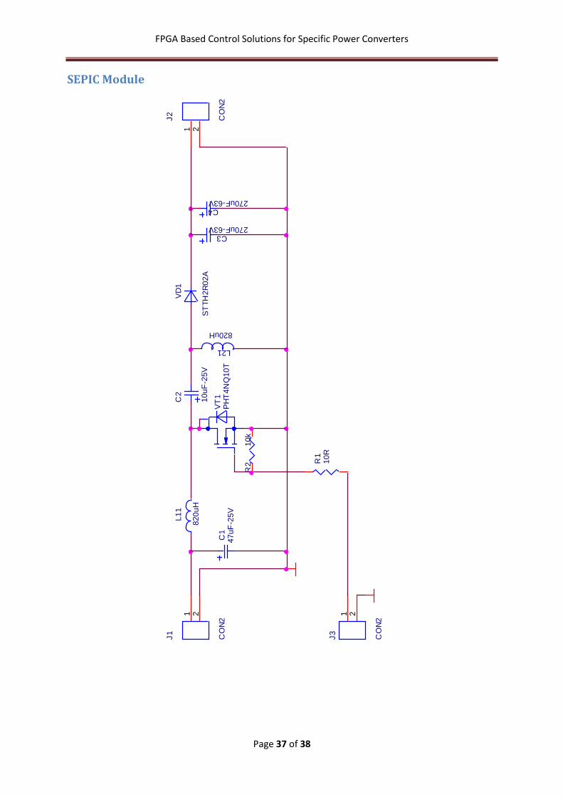
FPGA Based Control Solutions for Specific Power Converters
Page 37 of 38
SEPIC Module
R2
10
k
C4270uF-63V
VD
1
ST
TH
2R
02
A
J3
CO
N2
1 2
J1
CO
N2
1 2
C3270uF-63V
R1
10
R
L1
1
82
0u
H
C1
47
uF
-25
V
L21
820uH
VT
1P
HT
4N
Q1
0T
J2
CO
N2
1 2
C2
10
uF
-25
V

FPGA Based Control Solutions for Specific Power Converters
Page 38 of 38
References
[1] Dongbing Zhang, “Designing a SEPIC Converter”, Application Note 1484 for LM3478 and
LM3488 ICs (document SNVA168D), http://www.ti.com/lit/an/snva168d/snva168d.pdf,
last checked 2012, December 6.
[2] “1MSPS, 12-/10-/8-Bit A/D Converters in SOT-23 & LLP”, Datasheet for ADCS7476,
ADCS7477 and ADCS7478 ICs (document SNAS192E),
http://www.ti.com/lit/ds/symlink/adcs7476.pdf, last checked 2012, December 6.
[3] “2.7V 4-Channel/8-Channel 10-Bit A/D Converters with SPI™ Serial Interface”, Datasheet
for MCP3004/3008 ICs (document DS21295C),
http://ww1.microchip.com/downloads/en/DeviceDoc/21295C.pdf, last checked 2012,
December 6.
[4] Valery D. Yurkevich, “Advances in PID Control”, ISBN 978-953-307-267-8, 274 pages,
Publisher: InTech, Published: September 06, 2011 under CC BY-NC-SA 3.0 license
[5] IEEE Std 1076-1987, IEEE Standard VHDL Language Reference Manual
[6] В. П. Бабак, А. Г. Корченко, Н. П. Тимошенко, С. Ф. Филоненко, “VHDL. Справочное
пособие по основам языка”, ISBN 978-5-94120-169-3, изд. “Додэка XXI”, 224. стр.,
2008.