enc28j60 data sheet -...
TRANSCRIPT

2004 Microchip Technology Inc. Advance Information DS39662A
ENC28J60Data Sheet
Stand-Alone Ethernet Controllerwith SPI™ Interface
Note the following details of the code protection feature on Microchip devices:
• Microchip products meet the specification contained in their particular Microchip Data Sheet.
• Microchip believes that its family of products is one of the most secure families of its kind on the market today, when used in the intended manner and under normal conditions.
• There are dishonest and possibly illegal methods used to breach the code protection feature. All of these methods, to our knowledge, require using the Microchip products in a manner outside the operating specifications contained in Microchip’s Data Sheets. Most likely, the person doing so is engaged in theft of intellectual property.
• Microchip is willing to work with the customer who is concerned about the integrity of their code.
• Neither Microchip nor any other semiconductor manufacturer can guarantee the security of their code. Code protection does not mean that we are guaranteeing the product as “unbreakable.”
Code protection is constantly evolving. We at Microchip are committed to continuously improving the code protection features of ourproducts. Attempts to break Microchip’s code protection feature may be a violation of the Digital Millennium Copyright Act. If such actsallow unauthorized access to your software or other copyrighted work, you may have a right to sue for relief under that Act.
Information contained in this publication regarding deviceapplications and the like is provided only for your convenienceand may be superseded by updates. It is your responsibility toensure that your application meets with your specifications.MICROCHIP MAKES NO REPRESENTATIONS OR WAR-RANTIES OF ANY KIND WHETHER EXPRESS OR IMPLIED,WRITTEN OR ORAL, STATUTORY OR OTHERWISE,RELATED TO THE INFORMATION, INCLUDING BUT NOTLIMITED TO ITS CONDITION, QUALITY, PERFORMANCE,MERCHANTABILITY OR FITNESS FOR PURPOSE.Microchip disclaims all liability arising from this information andits use. Use of Microchip’s products as critical components inlife support systems is not authorized except with expresswritten approval by Microchip. No licenses are conveyed,implicitly or otherwise, under any Microchip intellectual propertyrights.
DS39662A-page ii Advance Info
Trademarks
The Microchip name and logo, the Microchip logo, Accuron, dsPIC, KEELOQ, microID, MPLAB, PIC, PICmicro, PICSTART, PRO MATE, PowerSmart, rfPIC, and SmartShunt are registered trademarks of Microchip Technology Incorporated in the U.S.A. and other countries.
AmpLab, FilterLab, Migratable Memory, MXDEV, MXLAB, PICMASTER, SEEVAL, SmartSensor and The Embedded Control Solutions Company are registered trademarks of Microchip Technology Incorporated in the U.S.A.
Analog-for-the-Digital Age, Application Maestro, dsPICDEM, dsPICDEM.net, dsPICworks, ECAN, ECONOMONITOR, FanSense, FlexROM, fuzzyLAB, In-Circuit Serial Programming, ICSP, ICEPIC, MPASM, MPLIB, MPLINK, MPSIM, PICkit, PICDEM, PICDEM.net, PICLAB, PICtail, PowerCal, PowerInfo, PowerMate, PowerTool, rfLAB, rfPICDEM, Select Mode, Smart Serial, SmartTel and Total Endurance are trademarks of Microchip Technology Incorporated in the U.S.A. and other countries.
SQTP is a service mark of Microchip Technology Incorporated in the U.S.A.
All other trademarks mentioned herein are property of their respective companies.
© 2004, Microchip Technology Incorporated, Printed in the U.S.A., All Rights Reserved.
Printed on recycled paper.
rmation 2004 Microchip Technology Inc.
Microchip received ISO/TS-16949:2002 quality system certification for its worldwide headquarters, design and wafer fabrication facilities in Chandler and Tempe, Arizona and Mountain View, California in October 2003. The Company’s quality system processes and procedures are for its PICmicro® 8-bit MCUs, KEELOQ® code hopping devices, Serial EEPROMs, microperipherals, nonvolatile memory and analog products. In addition, Microchip’s quality system for the design and manufacture of development systems is ISO 9001:2000 certified.

ENC28J60Stand-Alone Ethernet Controller with SPI™ Interface
Ethernet Controller Features
• IEEE 802.3 compatible Ethernet controller
• Integrated MAC and 10BASE-T PHY• Receiver and collision squelch circuit• Supports one 10BASE-T port with automatic
polarity detection and correction• Supports Full and Half-Duplex modes
• Programmable automatic retransmit on collision• Programmable padding and CRC generation• Programmable automatic rejection of erroneous
packets• SPI™ Interface with speeds up to 10 Mb/s
Buffer
• 8-Kbyte transmit/receive packet dual port SRAM
• Configurable transmit/receive buffer size• Hardware-managed circular receive FIFO• Byte-wide random and sequential access with
auto-increment• Internal DMA for fast data movement
• Hardware assisted IP checksum calculation
Medium Access Controller (MAC) Features
• Supports Unicast, Multicast and Broadcast packets
• Programmable receive packet filtering and wake-up host on logical AND or OR of the following:
- Unicast destination address- Multicast address- Broadcast address
- Magic Packet™- Group destination addresses as defined by
64-bit hash table- Programmable pattern matching of up to
64 bytes at user-defined offset• Loopback mode
Physical Layer (PHY) Features
• Wave shaping output filter• Loopback mode
Operational
• Two programmable LED outputs for LINK, TX, RX, collision and full/half-duplex status
• Seven interrupt sources with two interrupt pins
• 25 MHz clock• Clock out pin with programmable prescaler• Operating voltage range of 3.14V to 3.45V
• TTL level inputs• Temperature range: -40°C to +85°C Industrial,
0°C to +70°C Commercial (SSOP only)• 28-pin SPDIP, SSOP, SOIC, QFN packages
Package Types
EN
C28
J60
28-Pin SPDIP, SSOP, SOIC
1234567891011121314 15
161718192021222324
25262728
OSC2OSC1
LED
ALE
DB
TP
IN+
TP
IN-
INT
WOL 1
234567
8 9 10
28 27 26 25 24 23 22
212019
ENC28J60
11 12 13 14
18171615
VDDOSC
VD
DT
X
TP
OU
T+
TP
OU
T-
28-pin QFN
RESETCS
SOSI
SCK
RB
IAS
VSSRX
CLK
OU
T
VC
AP
VDDRX
VSSOSC
VDDPLL
VSSPLL
VS
ST
X
VD
D
VS
S
VCAP
OSC2OSC1
VDDRX
VSSTX
TPOUT+TPOUT-
LEDALEDBVDDOSC
VSSOSC
VDDTX
VDDPLL
VSSPLL
CLKOUT
RESETCS
SOSI
TPIN+TPIN-
RBIAS
INTWOL
SCK
VDD
VSS
VSSRX
2004 Microchip Technology Inc. Advance Information DS39662A-page 1

ENC28J60
Table of Contents
1.0 Overview ...................................................................................................................................................................................... 32.0 External Connections ................................................................................................................................................................... 53.0 Memory Organization ................................................................................................................................................................. 114.0 Serial Peripheral Interface (SPI)................................................................................................................................................. 255.0 Ethernet Overview...................................................................................................................................................................... 316.0 Initialization................................................................................................................................................................................. 337.0 Transmitting and Receiving Packets .......................................................................................................................................... 398.0 Receive Filters............................................................................................................................................................................ 479.0 Duplex Mode Configuration and Negotiation.............................................................................................................................. 5310.0 Flow Control ............................................................................................................................................................................... 5511.0 Reset .......................................................................................................................................................................................... 5912.0 Interrupts .................................................................................................................................................................................... 6513.0 Direct Memory Access Controller ............................................................................................................................................... 7514.0 Power-Down............................................................................................................................................................................... 7715.0 Built-in Self-Test Controller ........................................................................................................................................................ 7916.0 Electrical Characteristics ............................................................................................................................................................ 8317.0 Packaging Information................................................................................................................................................................ 89Index .................................................................................................................................................................................................... 95On-Line Support................................................................................................................................................................................... 97Systems Information and Upgrade Hot Line ........................................................................................................................................ 97Reader Response ................................................................................................................................................................................ 98Product Identification System............................................................................................................................................................... 99
TO OUR VALUED CUSTOMERS
It is our intention to provide our valued customers with the best documentation possible to ensure successful use of your Microchipproducts. To this end, we will continue to improve our publications to better suit your needs. Our publications will be refined andenhanced as new volumes and updates are introduced.
If you have any questions or comments regarding this publication, please contact the Marketing Communications Department viaE-mail at [email protected] or fax the Reader Response Form in the back of this data sheet to (480) 792-4150. Wewelcome your feedback.
Most Current Data SheetTo obtain the most up-to-date version of this data sheet, please register at our Worldwide Web site at:
http://www.microchip.com
You can determine the version of a data sheet by examining its literature number found on the bottom outside corner of any page.The last character of the literature number is the version number, (e.g., DS30000A is version A of document DS30000).
ErrataAn errata sheet, describing minor operational differences from the data sheet and recommended workarounds, may exist for currentdevices. As device/documentation issues become known to us, we will publish an errata sheet. The errata will specify the revisionof silicon and revision of document to which it applies.
To determine if an errata sheet exists for a particular device, please check with one of the following:
• Microchip’s Worldwide Web site; http://www.microchip.com• Your local Microchip sales office (see last page)When contacting a sales office, please specify which device, revision of silicon and data sheet (include literature number) you areusing.
Customer Notification SystemRegister on our web site at www.microchip.com to receive the most current information on all of our products.
DS39662A-page 2 Advance Information 2004 Microchip Technology Inc.

ENC28J60
1.0 OVERVIEW
The ENC28J60 is a stand-alone Ethernet controllerwith an industry standard Serial Peripheral Interface(SPI™). It is designed to serve as an Ethernet networkinterface for any controller equipped with SPI.
The ENC28J60 meets all of the IEEE 802.3 specifica-tions. It incorporates a number of packet filteringschemes to limit incoming packets. It also provides aninternal DMA module for fast data throughput and hard-ware assisted IP checksum calculations. Communica-tion with the host controller is implemented via twointerrupt pins and the SPI, with data rates of up to10 Mb/s. Two dedicated pins are used for LED link andnetwork activity indication.
A simple block diagram of the ENC28J60 is shown inFigure 1-1. A typical application circuit using the deviceis shown in Figure 1-2. With the ENC28J60, two pulsetransformers and a few passive components are all thatis required to connect a microcontroller to a 10 MbpsEthernet network.
The ENC28J60 consists of seven major functionalblocks:
1. An SPI interface that serves as a communica-tion channel between the host controller and theENC28J60.
2. Control Registers which are used to control andmonitor the ENC28J60.
3. A dual port RAM buffer for received andtransmitted data packets.
4. An arbiter to control the access to the RAMbuffer when requests are made from DMA,transmit and receive blocks.
5. The bus interface that interprets data andcommands received via the SPI interface.
6. The MAC (Medium Access Control) module thatimplements IEEE 802.3 compliant MAC logic.
7. The PHY (Physical Layer) module that encodesand decodes the analog data that is present onthe twisted pair interface.
The device also contains other support blocks, such asthe oscillator, on-chip voltage regulator, level translatorsto provide 5V tolerant I/Os and system control logic.
FIGURE 1-1: ENC28J60 BLOCK DIAGRAM
Dual Port RAM8 Kbytes
DMA &IP Checksum
TXBM
RXBM
Arbiter
Flow Control
Host Interface
ControlRegisters
25 MHzPower-on
PHY
Bus Interface
SPI
RMIIInterface
MIIMInterface
TPOUT+
TPOUT-
TPIN+
TPIN-
TX
RX
RBIAS
OSC1
OSC2VoltageSystem Control
CS(1)
SI(1)
SO
SCK(1)
INT
WOL
VCAP
CLKOUT
LEDA
LEDB
RESET(1)
RXF (Filter)
RX
TX
MAC
ch0
ch1
ch0
ch1
Buffer
Note 1: These pins are 5V tolerant.
RegulatorResetOscillator
2004 Microchip Technology Inc. Advance Information DS39662A-page 3
ENC28J60
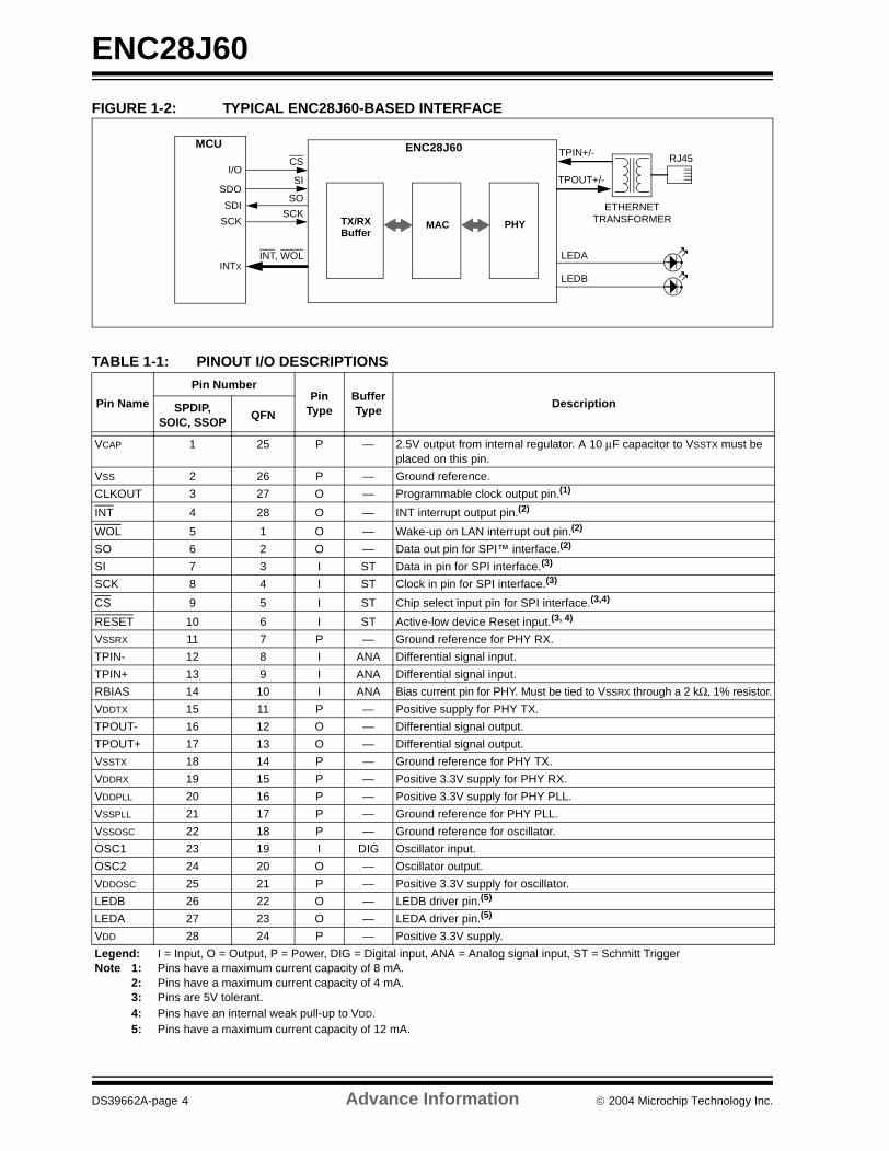
FIGURE 1-2: TYPICAL ENC28J60-BASED INTERFACE
TABLE 1-1: PINOUT I/O DESCRIPTIONS
Pin Name
Pin NumberPin
TypeBufferType
DescriptionSPDIP, SOIC, SSOP
QFN
VCAP 1 25 P — 2.5V output from internal regulator. A 10 µF capacitor to VSSTX must be placed on this pin.
VSS 2 26 P — Ground reference.
CLKOUT 3 27 O — Programmable clock output pin.(1)
INT 4 28 O — INT interrupt output pin.(2)
WOL 5 1 O — Wake-up on LAN interrupt out pin.(2)
SO 6 2 O — Data out pin for SPI™ interface.(2)
SI 7 3 I ST Data in pin for SPI interface.(3)
SCK 8 4 I ST Clock in pin for SPI interface.(3)
CS 9 5 I ST Chip select input pin for SPI interface.(3,4)
RESET 10 6 I ST Active-low device Reset input.(3, 4)
VSSRX 11 7 P — Ground reference for PHY RX.
TPIN- 12 8 I ANA Differential signal input.
TPIN+ 13 9 I ANA Differential signal input.
RBIAS 14 10 I ANA Bias current pin for PHY. Must be tied to VSSRX through a 2 kΩ, 1% resistor.
VDDTX 15 11 P — Positive supply for PHY TX.
TPOUT- 16 12 O — Differential signal output.
TPOUT+ 17 13 O — Differential signal output.
VSSTX 18 14 P — Ground reference for PHY TX.
VDDRX 19 15 P — Positive 3.3V supply for PHY RX.
VDDPLL 20 16 P — Positive 3.3V supply for PHY PLL.
VSSPLL 21 17 P — Ground reference for PHY PLL.
VSSOSC 22 18 P — Ground reference for oscillator.
OSC1 23 19 I DIG Oscillator input.
OSC2 24 20 O — Oscillator output.
VDDOSC 25 21 P — Positive 3.3V supply for oscillator.
LEDB 26 22 O — LEDB driver pin.(5)
LEDA 27 23 O — LEDA driver pin.(5)
VDD 28 24 P — Positive 3.3V supply.
Legend: I = Input, O = Output, P = Power, DIG = Digital input, ANA = Analog signal input, ST = Schmitt TriggerNote 1: Pins have a maximum current capacity of 8 mA.
2: Pins have a maximum current capacity of 4 mA.3: Pins are 5V tolerant.4: Pins have an internal weak pull-up to VDD.5: Pins have a maximum current capacity of 12 mA.
TRANSFORMER
MCU
TX/RX Buffer
MAC PHY
LEDA
LEDB
SI
SO
SCK
INT, WOL
SDO
SDI
SCK
INTX
ENC28J60 TPIN+/-
TPOUT+/-
ETHERNET
RJ45I/O
CS
DS39662A-page 4 Advance Information 2004 Microchip Technology Inc.

ENC28J60
2.0 EXTERNAL CONNECTIONS
2.1 Oscillator
The ENC28J60 is designed to operate at 25 MHz witha crystal connected to the OSC1 and OSC2 pins. TheENC28J60 design requires the use of a parallel cutcrystal. Use of a series cut crystal may give a frequencyout of the crystal manufacturer specifications. A typicaloscillator circuit is shown in Figure 2-1.
The ENC28J60 may also be driven by an external clocksource connected to the OSC1 pin as shown inFigure 2-2.
FIGURE 2-1: CRYSTAL OSCILLATOR OPERATION
FIGURE 2-2: EXTERNAL CLOCK SOURCE(1)
2.2 Oscillator Start-up Timer
The ENC28J60 contains an Oscillator Start-up Timer(OST) to ensure that the oscillator and integrated PHYhave stabilized before use. The OST does not expireuntil 7500 OSC1 clock cycles (300 µs) pass afterPower-on Reset or wake-up from Power-Down modeoccurs. During the delay, all Ethernet registers andbuffer memory may still be read and written to throughthe SPI bus. However, software should not attempt totransmit any packets (set ECON1.TXRTS), enablereception of packets (set ECON1.RXEN) or access anyMAC, MII or PHY registers during this period.
When the OST expires, the CLKRDY bit in the ESTATregister will be set. The application software should pollthis bit as necessary to determine when normal deviceoperation can begin.
C1
C2
XTAL
OSC2RS(1)
OSC1
RF(2)
To Internal Logic
Note 1: A series resistor, RS, may be required for ATstrip cut crystals.
2: The feedback resistor, RF, is typically in therange of 2 to 10 MΩ.
ENC28J60
3.3V Clock fromExternal System
OSC1
OSC2Open(2)
Note 1: Duty cycle restrictions must be observed.
2: A resistor to ground may be used to reducesystem noise. This may increase systemcurrent.
ENC28J60
Note: After a Power-on Reset, or the ENC28J60is removed from Power-Down mode, theCLKRDY bit must be polled beforetransmitting packets, enabling packetreception or accessing any MAC, MII orPHY registers.
2004 Microchip Technology Inc. Advance Information DS39662A-page 5

ENC28J60
2.3 CLKOUT Pin
The clock out pin is provided to the system designer foruse as the host controller clock or as a clock source forother devices in the system. The CLKOUT has aninternal prescaler which can divide the output by 1, 2,3, 4 or 8. The CLKOUT function is enabled and theprescaler is selected via the ECOCON register(Register 2-1).
To create a clean clock signal, the CLKOUT pin is heldlow for a period when power is first applied. After thePower-on Reset ends, the OST will begin counting.When the OST expires, the CLKOUT pin will begin out-putting its default frequency of 6.25 MHz (main clockdivided by 4). At any future time that the ENC28J60 isreset by software or the RESET pin, the CLKOUT func-tion will not be altered (ECOCON will not change
value). Additionally, Power-Down mode may beentered and the CLKOUT function will continue tooperate. When Power-Down mode is cancelled, theOST will be reset but the CLKOUT function willcontinue. When the CLKOUT function is disabled(ECOCON = 0), the CLKOUT pin is driven low.
The CLKOUT function is designed to ensure that mini-mum timings are preserved when the CLKOUT pinfunction is enabled, disabled or the prescaler value ischanged. No high or low pulses will be outputted whichexceed the frequency specified by the ECOCONconfiguration. However, when switching frequencies, adelay between two and eight OSC1 clock periods willoccur where no clock pulses will be produced (seeFigure 2-3). During this period, CLKOUT will be heldlow.
FIGURE 2-3: CLKOUT TRANSITION
REGISTER 2-1: ECOCON: CLOCK OUTPUT CONTROL REGISTER
ECOCONChanged 80 ns to 320 ns Delay
U-0 U-0 U-0 U-0 U-0 R/W-1 R/W-0 R/W-0
— — — — — COCON2 COCON1 COCON0
bit 7 bit 0
bit 7-3 Unimplemented: Read as ‘0’
bit 2-0 COCON2:COCON0: Clock Output Configuration bits111 = Reserved for factory test. Do not use. Glitch prevention not assured.110 = Reserved for factory test. Do not use. Glitch prevention not assured.101 = CLKOUT outputs main clock divided by 8 (3.125 MHz)100 = CLKOUT outputs main clock divided by 4 (6.25 MHz)011 = CLKOUT outputs main clock divided by 3 (8.333333 MHz)010 = CLKOUT outputs main clock divided by 2 (12.5 MHz)001 = CLKOUT outputs main clock divided by 1 (25 MHz)000 = CLKOUT is disabled. The pin is driven low.
Legend:
R = Readable bit W = Writable bit U = Unimplemented bit, read as ‘0’
-n = Value at POR ‘1’ = Bit is set ‘0’ = Bit is cleared x = Bit is unknown
DS39662A-page 6 Advance Information 2004 Microchip Technology Inc.

ENC28J60
2.4 Magnetics, Termination and Other External Components
To complete the Ethernet interface, the ENC28J60requires several standard components to be installedexternally. These components should be connected asshown in Figure 2-4.
On the differential receive pins (TPIN+/TPIN-), a1:1 pulse transformer rated for 10BASE-T operation isrequired. On the differential transmit pins(TPOUT+/TPOUT-), a 1:1 pulse transformer with acenter tap is required. The transformers should berated for isolation of 2 kV or more to protect againststatic voltages. See Section 16.0 “Electrical Charac-teristics” for specific transformer requirements. Bothportions additionally require two 50Ω, 1% resistors anda 0.01 µF capacitor for proper termination.
The internal analog circuitry in the ENC28J60 requiresthat an external 2 kΩ, 1% resistor be attached fromRBIAS to ground.
Some of the digital circuitry in the ENC28J60 operatesat a nominal 2.5V to reduce power consumption. A2.5V regulator is incorporated internally to generate thenecessary voltage. The only external componentrequired is a 10 µF capacitor for stability purposes. Thiscapacitor should be attached from VCAP to ground. Theinternal regulator was not designed to drive externalloads.
All power supply pins must be externally connected tothe same 3.3V power source. Similarly, all groundreferences should be externally connected to the sameground node. Each VDD and VSS pin pair should havea 0.1 µF ceramic bypass capacitor placed as close tothe pins as possible. Relatively high currents are nec-essary to operate the twisted pair interface, so all wiresshould be kept as short as possible and reasonablewire widths should be used on power wires to reduceresistive loss.
FIGURE 2-4: EXTERNAL CONNECTIONS
I/OSCKSDOSDI
INT0INT1
MCU 5.0V ← 3.3VLevelShift
Logic(2)
CSSCKSISO
INTWOL
ENC28J60
VCAP LEDA LEDB RBIAS
TPOUT+
TPOUT-
TPIN+
TPIN-
1
2
3
4
5
6
7
8
RJ-45
1:1 CT
1:1
10 µF
2K1%
50Ω1%
FerriteBead(1)
0.01 µF
3.3V
0.01 µF
.001 µF2kV
Note 1: Ferrite Bead should be rated for at least 100 mA.
2: Required only if the microcontroller is operating at 5V.
50Ω
50Ω
50Ω
1%
1%
1%
2004 Microchip Technology Inc. Advance Information DS39662A-page 7

ENC28J60
2.5 I/O Levels
The ENC28J60 is a 3.3V part; however, it wasdesigned to be easily integrated into 5V systems. TheSPI CS, SCK and SI inputs, as well as the RESET pin,are all 5V tolerant. On the other hand, if the hostcontroller is operated at 5V, it quite likely will not bewithin specifications when its SPI and interrupt inputsare driven by the 3.3V CMOS outputs on theENC28J60. A unidirectional level translator would benecessary.
An economical 74HCT08 (quad AND gate), 74ACT125(quad 3-state buffer) or many other 5V CMOS chipswith TTL level input buffers may be used to provide thenecessary level shifting. The use of 3-state bufferspermits easy integration into systems which share theSPI bus with other devices. Figure 2-5 and Figure 2-6show example translation schemes.
FIGURE 2-5: LEVEL SHIFTING USING AND GATES
FIGURE 2-6: LEVEL SHIFTING USING 3-STATE BUFFERS
2.6 LED Configuration
The LEDA and LEDB pins support automatic polaritydetection on Reset. The LEDs can be connected suchthat the pin must source current to turn the LED on, oralternately connected such that the pin must sink cur-rent to turn the LED on. Upon system Reset, theENC28J60 will detect how the LED is connected andbegin driving the LED to the default state configured bythe PHLCON register. If the LED polarity is changedwhile the ENC28J60 is operating, the new polarity willnot be detected until the next system Reset occurs.
LEDB is unique in that the connection of the LED isautomatically read on Reset and determines how to ini-tialize the PHCON1.PDPXMD bit. If the pin sourcescurrent to illuminate the LED, the bit is cleared onReset and the PHY defaults to half-duplex operation. Ifthe pin sinks current to illuminate the LED, the bit is seton Reset and the PHY defaults to full-duplex operation.Figure 2-7 shows the two available options. If no LEDis attached to the LEDB pin, the PDPXMD bit will resetto an indeterminate value.
FIGURE 2-7: LEDB POLARITY AND RESET CONFIGURATION OPTIONS
I/O
SCK
SO
SI
INT0
INT1
MCU
CS
SCK
SI
SO
INT
WOL
ENC28J60
CLKOUTOSC1
I/O
SCK
SO
SI
INT0
INT1
MCU
CS
SCK
SI
SO
INT
WOL
ENC28J60
CLKOUTOSC1
LEDB
+3.3VFull-Duplex Operation:PDPXMD = 1
LEDB
Half-Duplex Operation:PDPXMD = 0
DS39662A-page 8 Advance Information 2004 Microchip Technology Inc.

ENC28J60
REGISTER 2-2: PHLCON: PHY MODULE LED CONTROL REGISTER
bit 15-12 Reserved: Write as ‘0’
bit 11-8 LACFG3:LACFG0: LEDA Configuration bits 0000 = Reserved0001 = Display transmit activity (stretchable)0010 = Display receive activity (stretchable)0011 = Display collision activity (stretchable)0100 = Display link status0101 = Display duplex status0110 = Reserved0111 = Display transmit and receive activity (stretchable)1000 = On1001 = Off1010 = Blink fast1011 = Blink slow1100 = Display link status and receive activity (always stretched)1101 = Display link status and transmit/receive activity (always stretched)1110 = Display duplex status and collision activity (always stretched)1111 = Reserved
bit 7-4 LBCFG3:LBCFG0: LEDB Configuration bits 0000 = Reserved0001 = Display transmit activity (stretchable)0010 = Display receive activity (stretchable)0011 = Display collision activity (stretchable)0100 = Display link status0101 = Display duplex status0110 = Reserved0111 = Display transmit and receive activity (stretchable)1000 = On1001 = Off1010 = Blink fast1011 = Blink slow1100 = Display link status and receive activity (always stretched)1101 = Display link status and transmit/receive activity (always stretched)1110 = Display duplex status and collision activity (always stretched)1111 = Reserved
bit 3-2 LFRQ1:LFRQ0: LED Pulse Stretch Time Configuration bits11 = Reserved10 = Stretch LED events to approximately 139 ms01 = Stretch LED events to approximately 73 ms00 = Stretch LED events to approximately 40 ms
bit 1 STRCH: LED Pulse Stretching Enable bit 1 = Stretchable LED events will cause lengthened LED pulses based on the LFRQ configuration0 = Stretchable LED events will only be displayed while they are occurring
bit 0 Reserved: Write as ‘0’
R/W-0 R/W-0 R/W-1 R/W-1 R/W-0 R/W-1 R/W-0 R/W-0
r r r r LACFG3 LACFG2 LACFG1 LACFG0
bit 15 bit 8
R/W-0 R/W-0 R/W-1 R/W-0 R/W-0 R/W-0 R/W-1 R/W-x
LBCFG3 LBCFG2 LBCFG1 LBCFG0 LFRQ1 LFRQ0 STRCH r
bit 7 bit 0
Legend:
R = Readable bit W = Writable bit r = Reserved bit
-n = Value at POR ‘1’ = Bit is set ‘0’ = Bit is cleared x = Bit is unknown
2004 Microchip Technology Inc. Advance Information DS39662A-page 9

ENC28J60
NOTES:
DS39662A-page 10 Advance Information 2004 Microchip Technology Inc.

ENC28J60
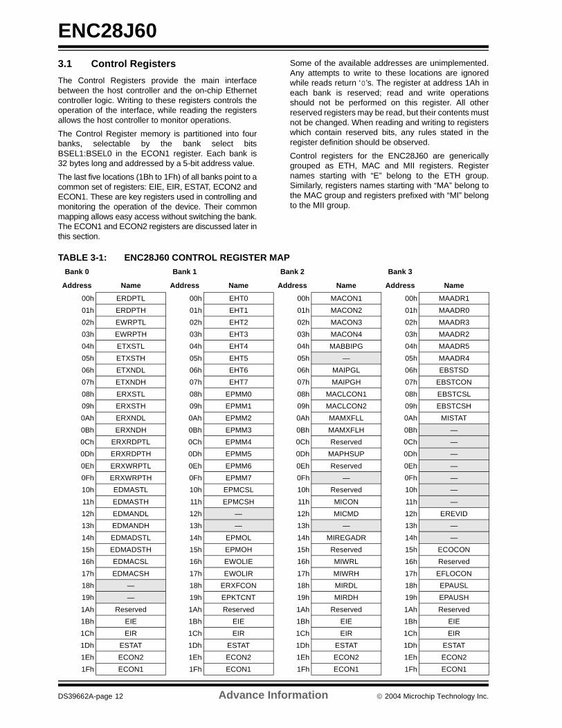
3.0 MEMORY ORGANIZATION
All memory in the ENC28J60 is implemented as staticRAM. There are three types of memory in theENC28J60:
• Control Registers• Ethernet Buffer
• PHY Registers
The control registers’ memory contains ControlRegisters (CRs). These are used for configuration,control and status retrieval of the ENC28J60. TheControl Registers are directly read and written to by theSPI interface.
The Ethernet buffer contains transmit and receivememory used by the Ethernet controller in a singlememory space. The sizes of the memory areas areprogrammable by the host controller using the SPIinterface. The Ethernet buffer memory can only beaccessed via the read buffer memory and write buffermemory SPI commands (see Section 4.2.2 “ReadBuffer Memory Command” and Section 4.2.4 “WriteBuffer Memory Command”).
The PHY registers are used for configuration, control andstatus retrieval of the PHY module. The registers are notdirectly accessible through the SPI interface; they canonly be accessed through the Media IndependentInterface (MII) implemented in the MAC.
Figure 3-1 shows the data memory organization for theENC28J60.
FIGURE 3-1: ENC28J60 MEMORY ORGANIZATION
Common Registers
Common Registers
Common Registers
Common Registers
00h
19h1Ah
1Fh00h
19h1Ah
1Fh00h
19h1Ah
1Fh00h
19h1Ah
1Fh
Bank 0
Bank 1
Bank 2
Bank 3
0000h
1FFFh
= 00
= 01
= 10
= 11
ECON1<1:0> Control Registers Ethernet Buffer
00h
1Fh
PHY Registers
Note: Memory areas are not shown to scale. The size of the control memory space has been scaled to show detail.
Buffer Pointers in Bank 0
2004 Microchip Technology Inc. Advance Information DS39662A-page 11
ENC28J60
3.1 Control RegistersThe Control Registers provide the main interfacebetween the host controller and the on-chip Ethernetcontroller logic. Writing to these registers controls theoperation of the interface, while reading the registersallows the host controller to monitor operations.
The Control Register memory is partitioned into fourbanks, selectable by the bank select bitsBSEL1:BSEL0 in the ECON1 register. Each bank is32 bytes long and addressed by a 5-bit address value.
The last five locations (1Bh to 1Fh) of all banks point to acommon set of registers: EIE, EIR, ESTAT, ECON2 andECON1. These are key registers used in controlling andmonitoring the operation of the device. Their commonmapping allows easy access without switching the bank.The ECON1 and ECON2 registers are discussed later inthis section.
Some of the available addresses are unimplemented.Any attempts to write to these locations are ignoredwhile reads return ‘0’s. The register at address 1Ah ineach bank is reserved; read and write operationsshould not be performed on this register. All otherreserved registers may be read, but their contents mustnot be changed. When reading and writing to registerswhich contain reserved bits, any rules stated in theregister definition should be observed.
Control registers for the ENC28J60 are genericallygrouped as ETH, MAC and MII registers. Registernames starting with “E” belong to the ETH group.Similarly, registers names starting with “MA” belong tothe MAC group and registers prefixed with “MI” belongto the MII group.
TABLE 3-1: ENC28J60 CONTROL REGISTER MAPBank 0 Bank 1 Bank 2 Bank 3
Address Name Address Name Address Name Address Name
00h ERDPTL 00h EHT0 00h MACON1 00h MAADR1
01h ERDPTH 01h EHT1 01h MACON2 01h MAADR0
02h EWRPTL 02h EHT2 02h MACON3 02h MAADR3
03h EWRPTH 03h EHT3 03h MACON4 03h MAADR2
04h ETXSTL 04h EHT4 04h MABBIPG 04h MAADR5
05h ETXSTH 05h EHT5 05h — 05h MAADR4
06h ETXNDL 06h EHT6 06h MAIPGL 06h EBSTSD
07h ETXNDH 07h EHT7 07h MAIPGH 07h EBSTCON
08h ERXSTL 08h EPMM0 08h MACLCON1 08h EBSTCSL
09h ERXSTH 09h EPMM1 09h MACLCON2 09h EBSTCSH
0Ah ERXNDL 0Ah EPMM2 0Ah MAMXFLL 0Ah MISTAT
0Bh ERXNDH 0Bh EPMM3 0Bh MAMXFLH 0Bh —
0Ch ERXRDPTL 0Ch EPMM4 0Ch Reserved 0Ch —
0Dh ERXRDPTH 0Dh EPMM5 0Dh MAPHSUP 0Dh —
0Eh ERXWRPTL 0Eh EPMM6 0Eh Reserved 0Eh —
0Fh ERXWRPTH 0Fh EPMM7 0Fh — 0Fh —
10h EDMASTL 10h EPMCSL 10h Reserved 10h —
11h EDMASTH 11h EPMCSH 11h MICON 11h —
12h EDMANDL 12h — 12h MICMD 12h EREVID
13h EDMANDH 13h — 13h — 13h —
14h EDMADSTL 14h EPMOL 14h MIREGADR 14h —
15h EDMADSTH 15h EPMOH 15h Reserved 15h ECOCON
16h EDMACSL 16h EWOLIE 16h MIWRL 16h Reserved
17h EDMACSH 17h EWOLIR 17h MIWRH 17h EFLOCON
18h — 18h ERXFCON 18h MIRDL 18h EPAUSL
19h — 19h EPKTCNT 19h MIRDH 19h EPAUSH
1Ah Reserved 1Ah Reserved 1Ah Reserved 1Ah Reserved
1Bh EIE 1Bh EIE 1Bh EIE 1Bh EIE
1Ch EIR 1Ch EIR 1Ch EIR 1Ch EIR
1Dh ESTAT 1Dh ESTAT 1Dh ESTAT 1Dh ESTAT
1Eh ECON2 1Eh ECON2 1Eh ECON2 1Eh ECON2
1Fh ECON1 1Fh ECON1 1Fh ECON1 1Fh ECON1
DS39662A-page 12 Advance Information 2004 Microchip Technology Inc.

ENC28J60
TABLE 3-2: ENC28J60 CONTROL REGISTER SUMMARY
Register Name Bit 7 Bit 6 Bit 5 Bit 4 Bit 3 Bit 2 Bit 1 Bit 0Value
onReset
Detailson
Page
EIE INTIE PKTIE DMAIE LINKIE TXIE WOLIE TXERIE RXERIE 0000 0000 67
EIR — PKTIF DMAIF LINKIF TXIF WOLIF TXERIF RXERIF -000 0000 68
ESTAT INT r r LATECOL — RXBUSY TXABRT CLKRDY(1) 0000 -000 66
ECON2 AUTOINC PKTDEC PWRSV — VRPS — — — 100- 0--- 16
ECON1 TXRST RXRST DMAST CSUMEN TXRTS RXEN BSEL1 BSEL0 0000 0000 15
ERDPTL Read Pointer Low Byte ERDPT<7:0>) 1111 1010 17
ERDPTH — — — Read Pointer High Byte (ERDPT<12:8>) ---0 0101 17
EWRPTL Write Pointer Low Byte (EWRPT<7:0>) 0000 0000 17
EWRPTH — — — Write Pointer High Byte (EWRPT<12:8>) ---0 0000 17
ETXSTL TX Start Low Byte (ETXST<7:0>) 0000 0000 17
ETXSTH — — — TX Start High Byte (ETXST<12:8>) ---0 0000 17
ETXNDL TX End Low Byte (ETXND<7:0>) 0000 0000 17
ETXNDH — — — TX End High Byte (ETXND<12:8>) ---0 0000 17
ERXSTL RX Start Low Byte (ERXST<7:0>) 1111 1010 17
ERXSTH — — — RX Start High Byte (ERXST<12:8>) ---0 0101 17
ERXNDL RX End Low Byte (ERXND<7:0>) 1111 1111 17
ERXNDH — — — RX End High Byte (ERXND<12:8>) ---1 1111 17
ERXRDPTL RX RD Pointer Low Byte (ERXRDPT<7:0>) 1111 1010 17
ERXRDPTH — — — RX RD Pointer High Byte (ERXRDPT<12:8>) ---0 0101 17
ERXWRPTL RX WR Pointer Low Byte (ERXWRPT<7:0>) 0000 0000 17
ERXWRPTH — — — RX WR Pointer High Byte (ERXWRPT<12:8>) ---0 0000 17
EDMASTL DMA Start Low Byte (EDMAST<7:0>) 0000 0000 75
EDMASTH — — — DMA Start High Byte (EDMAST<12:8>) ---0 0000 75
EDMANDL DMA End Low Byte (EDMAND<7:0>) 0000 0000 75
EDMANDH — — — DMA End High Byte (EDMAND<12:8>) ---0 0000 75
EDMADSTL DMA Destination Low Byte (EDMADST<7:0>) 0000 0000 75
EDMADSTH — — — DMA Destination High Byte (EDMADST<12:8>) ---0 0000 75
EDMACSL DMA Checksum Low Byte (EDMACS<7:0>) 0000 0000 76
EDMACSH DMA Checksum High Byte (EDMACS<15:8>) 0000 0000 76
EHT0 Hash Table Byte 0 (EHT<7:0>) 0000 0000 52
EHT1 Hash Table Byte 1 (EHT<15:8>) 0000 0000 52
EHT2 Hash Table Byte 2 (EHT<23:16>) 0000 0000 52
EHT3 Hash Table Byte 3 (EHT<31:24>) 0000 0000 52
EHT4 Hash Table Byte 4 (EHT<39:32>) 0000 0000 52
EHT5 Hash Table Byte 5 (EHT<47:40>) 0000 0000 52
EHT6 Hash Table Byte 6 (EHT<55:48>) 0000 0000 52
EHT7 Hash Table Byte 7 (EHT<63:56>) 0000 0000 52
EPMM0 Pattern Match Mask Byte 0 (EPMM<7:0>) 0000 0000 51
EPMM1 Pattern Match Mask Byte 1 (EPMM<15:8>) 0000 0000 51
EPMM2 Pattern Match Mask Byte 2 (EPMM<23:16>) 0000 0000 51
EPMM3 Pattern Match Mask Byte 3 (EPMM<31:24>) 0000 0000 51
EPMM4 Pattern Match Mask Byte 4 (EPMM<39:32>) 0000 0000 51
EPMM5 Pattern Match Mask Byte 5 (EPMM<47:40>) 0000 0000 51
EPMM6 Pattern Match Mask Byte 6 (EPMM<55:48>) 0000 0000 51
EPMM7 Pattern Match Mask Byte 7 (EPMM<63:56>) 0000 0000 51
EPMCSL Pattern Match Checksum Low Byte (EPMCS<7:0>) 0000 0000 51
EPMCSH Pattern Match Checksum High Byte (EPMCS<15:0>) 0000 0000 51
Legend: x = unknown, u = unchanged, — = unimplemented, q = value depends on condition, r = reserved, do not modify.Note 1: CLKRDY resets to ‘0’ on Power-on Reset but is unaffected on all other Resets.
2: EREVID is a read-only register.3: ECOCON resets to ‘---- -100’ on Power-on Reset and ‘---- -uuu’ on all other Resets.
2004 Microchip Technology Inc. Advance Information DS39662A-page 13

ENC28J60
EPMOL Pattern Match Offset Low Byte (EPMO<7:0>) 0000 0000 51
EPMOH — — — Pattern Match Offset High Byte (EPMO<12:8>) ---0 0000 51
EWOLIE UCWOLIE AWOLIE — PMWOLIE MPWOLIE HTWOLIE MCWOLIE BCWOLIE 00-0 0000 72
EWOLIR UCWOLIF AWOLIF — PMWOLIF MPWOLIF HTWOLIF MCWOLIF BCWOLIF 00-0 0000 73
ERXFCON UCEN ANDOR CRCEN PMEN MPEN HTEN MCEN BCEN 1010 0001 48
EPKTCNT Ethernet Packet Count 0000 0000 43
MACON1 — — — LOOPBK TXPAUS RXPAUS PASSALL MARXEN ---0 0000 34
MACON2 MARST RNDRST — — MARXRST RFUNRST MATXRST TFUNRST 10-- 0000 61
MACON3 PADCFG2 PADCFG1 PADCFG0 TXCRCEN PHDRLEN HFRMEN FRMLNEN FULDPX 0000 0000 35
MACON4 — DEFER BPEN NOBKOFF — — LONGPRE PUREPRE -000 --00 36
MABBIPG — Back-to-Back Inter-Packet Gap (BBIPG<6:0>) -000 0000 37
MAIPGL — Non-Back-to-Back Inter-Packet Gap Low Byte (MAIPGL<6:0>) -000 0000 34
MAIPGH — Non-Back-to-Back Inter-Packet Gap High Byte (MAIPGH<6:0>) -000 0000 34
MACLCON1 — — — — Retransmission Maximum (RETMAX<3:0>) ---- 1111 34
MACLCON2 — — Collision Window (COLWIN<5:0>) --11 0111 34
MAMXFLL Maximum Frame Length Low Byte (MAMXFL<7:0>) 0000 0000 34
MAMXFLH Maximum Frame Length High Byte (MAMXFL<15:8>) 0000 0110 34
MAPHSUP RSTINTFC — — r RSTRMII — — r 0--1 0--0 62
MICON RSTMII — — — — — — — 0--- ---- 21
MICMD — — — — — — MIISCAN MIIRD ---- --00 21
MIREGADR — — — MII Register Address (MIREGADR<4:0>) ---0 0000 19
MIWRL MII Write Data Low Byte (MIWR<7:0>) 0000 0000 19
MIWRH MII Write Data High Byte (MIWR<15:8>) 0000 0000 19
MIRDL MII Read Data Low Byte (MIRD<7:0>) 0000 0000 19
MIRDH MII Read Data High Byte(MIRD<15:8>) 0000 0000 19
MAADR1 MAC Address Byte 1 (MAADR<15:8>) 0000 0000 34
MAADR0 MAC Address Byte 0 (MAADR<7:0>) 0000 0000 34
MAADR3 MAC Address Byte 3 (MAADR<31:24>) 0000 0000 34
MAADR2 MAC Address Byte 2(MAADR<23:16>) 0000 0000 34
MAADR5 MAC Address Byte 5 (MAADR<48:41>) 0000 0000 34
MAADR4 MAC Address Byte 4 (MAADR<40:32>) 0000 0000 34
EBSTSD Built-in Self-Test Fill Seed (EBSTSD<7:0>) 0000 0000 80
EBSTCON PSV2 PSV1 PSV0 PSEL TMSEL1 TMSEL0 TME BISTST 0000 0000 79
EBSTCSL Built-in Self-Test Checksum Low Byte (EBSTCS<7:0>) 0000 0000 80
EBSTCSH Built-in Self-Test Checksum High Byte (EBSTCS<15:8>) 0000 0000 80
MISTAT — — — — r NVALID SCAN BUSY ---- 0000 22
EREVID(2) — — — Ethernet Revision ID (EREVID<4:0>) ---q qqqq 22
ECOCON(3) — — — — — COCON2 COCON1 COCON0 ---- -100 6
EFLOCON — — — — — FULDPXS FCEN1 FCEN0 ---- -000 56
EPAUSL Pause Timer Value Low Byte (EPAUS<7:0>) 0000 0000 57
EPAUSH Pause Timer Value High Byte (EPAUS<15:8>) 0001 0000 57
TABLE 3-2: ENC28J60 CONTROL REGISTER SUMMARY (CONTINUED)
Register Name Bit 7 Bit 6 Bit 5 Bit 4 Bit 3 Bit 2 Bit 1 Bit 0Value
onReset
Detailson
Page
Legend: x = unknown, u = unchanged, — = unimplemented, q = value depends on condition, r = reserved, do not modify.Note 1: CLKRDY resets to ‘0’ on Power-on Reset but is unaffected on all other Resets.
2: EREVID is a read-only register.3: ECOCON resets to ‘---- -100’ on Power-on Reset and ‘---- -uuu’ on all other Resets.
DS39662A-page 14 Advance Information 2004 Microchip Technology Inc.

ENC28J60
3.1.1 ECON1 REGISTER
The ECON1 register, shown in Register 3-1, is used tocontrol the main functions of the ENC28J60. Receiveenable, transmit request, DMA control and bank selectbits can all be found in ECON1.
REGISTER 3-1: ECON1: ETHERNET CONTROL REGISTER 1 R/W-0 R/W-0 R/W-0 R/W-0 R/W-0 R/W-0 R/W-0 R/W-0
TXRST RXRST DMAST CSUMEN TXRTS RXEN BSEL1 BSEL0
bit 7 bit 0
bit 7 TXRST: Transmit Logic Reset bit1 = Transmit logic is held in Reset0 = Normal operation
bit 6 RXRST: Receive Logic Reset bit
1 = Receive logic is held in Reset0 = Normal operation
bit 5 DMAST: DMA Start and Busy Status bit1 = DMA copy or checksum operation is in progress0 = DMA hardware is Idle
bit 4 CSUMEN: DMA Checksum Enable bit1 = DMA hardware calculates checksums0 = DMA hardware copies buffer memory
bit 3 TXRTS: Transmit Request To Send bit
1 = The transmit logic is attempting to transmit a packet0 = The transmit logic is Idle
bit 2 RXEN: Receive Enable bit1 = Packets which pass the current filter configuration will be written into the receive buffer0 = All packets received will be ignored
bit 1-0 BSEL1:BSEL0: Bank Select bits11 = SPI accesses registers in Bank 310 = SPI accesses registers in Bank 201 = SPI accesses registers in Bank 100 = SPI accesses registers in Bank 0
Legend:
R = Readable bit W = Writable bit U = Unimplemented bit, read as ‘0’
-n = Value at POR ‘1’ = Bit is set ‘0’ = Bit is cleared x = Bit is unknown
2004 Microchip Technology Inc. Advance Information DS39662A-page 15
ENC28J60
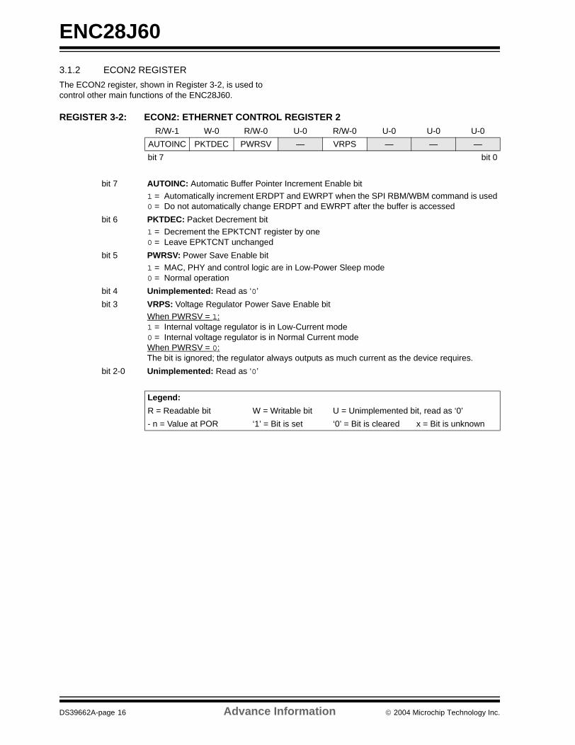
3.1.2 ECON2 REGISTER
The ECON2 register, shown in Register 3-2, is used tocontrol other main functions of the ENC28J60.
REGISTER 3-2: ECON2: ETHERNET CONTROL REGISTER 2 R/W-1 W-0 R/W-0 U-0 R/W-0 U-0 U-0 U-0
AUTOINC PKTDEC PWRSV — VRPS — — —
bit 7 bit 0
bit 7 AUTOINC: Automatic Buffer Pointer Increment Enable bit
1 = Automatically increment ERDPT and EWRPT when the SPI RBM/WBM command is used0 = Do not automatically change ERDPT and EWRPT after the buffer is accessed
bit 6 PKTDEC: Packet Decrement bit1 = Decrement the EPKTCNT register by one0 = Leave EPKTCNT unchanged
bit 5 PWRSV: Power Save Enable bit1 = MAC, PHY and control logic are in Low-Power Sleep mode0 = Normal operation
bit 4 Unimplemented: Read as ‘0’
bit 3 VRPS: Voltage Regulator Power Save Enable bitWhen PWRSV = 1:1 = Internal voltage regulator is in Low-Current mode0 = Internal voltage regulator is in Normal Current modeWhen PWRSV = 0:The bit is ignored; the regulator always outputs as much current as the device requires.
bit 2-0 Unimplemented: Read as ‘0’
Legend:
R = Readable bit W = Writable bit U = Unimplemented bit, read as ‘0’
- n = Value at POR ‘1’ = Bit is set ‘0’ = Bit is cleared x = Bit is unknown
DS39662A-page 16 Advance Information 2004 Microchip Technology Inc.

ENC28J60
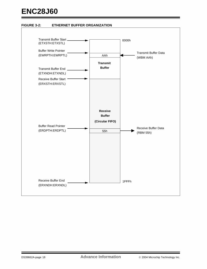
3.2 Ethernet Buffer
The Ethernet buffer contains transmit and receivememory used by the Ethernet controller. The entirebuffer is 8 Kbytes, divided into separate receive andtransmit buffer spaces. The sizes and locations oftransmit and receive memory are fully programmableby the host controller using the SPI interface.
The relationship of the buffer spaces is shown inFigure 3-2.
3.2.1 RECEIVE BUFFER
The receive buffer constitutes a circular FIFO buffermanaged by hardware. The register pairsERXSTH:ERXSTL and ERXNDH:ERXNDL serve aspointers to define the buffer’s size and location withinthe memory. The byte pointed to by ERXST and thebyte pointed to by ERXND are both included in theFIFO buffer.
As bytes of data are received from the Ethernetinterface, they are written into the receive buffersequentially. However, after the memory pointed to byERXND is written to, the hardware will automaticallywrite the next byte of received data to the memorypointed to by ERXST. As a result, the receive hardwarewill never write outside the boundaries of the FIFO.
The host controller may program the ERXST andERXND pointers when the receive logic is not enabled.The pointers must not be modified while the receivelogic is enabled (ECON1.RXEN is set). If desired, thepointers may span the 1FFFh to 0000h memoryboundary; the hardware will still operate as a FIFO.
The ERXWRPTH:ERXWRPTL registers define alocation within the FIFO where the hardware will writebytes that it receives. The pointer is read-only and isautomatically updated by the hardware whenever anew packet is successfully received. The pointer isuseful for determining how much free space isavailable within the FIFO.
The ERXRDPT registers define a location within theFIFO where the receive hardware is forbidden to writeto. In normal operation, the receive hardware will writedata up to, but not including, the memory pointed to byERXRDPT. If the FIFO fills up with data and new datacontinues to arrive, the hardware will not overwrite thepreviously received data. Instead, the new data will bethrown away and the old data will be preserved. Inorder to continuously receive new data, the host con-troller must periodically advance this pointer wheneverit finishes processing some, or all, of the old receiveddata.
3.2.2 TRANSMIT BUFFER
Any space within the 8-Kbyte memory, which is notprogrammed as part of the receive FIFO buffer, isconsidered to be the transmit buffer. The responsibilityof managing where packets are located in the transmitbuffer belongs to the host controller. Whenever the hostcontroller decides to transmit a packet, the ETXST andETXND pointers are programmed with addressesspecifying where, within the transmit buffer, the partic-ular packet to transmit is located. The hardware doesnot check that the start and end addresses do notoverlap with the receive buffer. To prevent buffercorruption, the host controller must make sure to nottransmit a packet while the ETXST and ETXNDpointers are overlapping the receive buffer, or while theETXND pointer is too close to the receive buffer. SeeSection 7.1 “Transmitting Packets” for moreinformation.
3.2.3 READING AND WRITING TO THE BUFFER
The Ethernet buffer contents are accessed from thehost controller though separate read and write pointers(ERDPT and EWRPT) combined with the read buffermemory and write buffer memory SPI commands.While sequentially reading from the receive buffer, awrapping condition will occur at the end of the receivebuffer. While sequentially writing to the buffer, no wrap-ping conditions will occur. See Section 4.2.2 “ReadBuffer Memory Command” and Section 4.2.4 “WriteBuffer Memory Command” for more information.
3.2.4 DMA ACCESS TO THE BUFFER
The integrated DMA controller must read from the bufferwhen calculating a checksum and it must read and writeto the buffer when copying memory. The DMA followsthe same wrapping rules that SPI accesses do. While itsequentially reads, it will be subject to a wrapping condi-tion at the end of the receive buffer. All writes it does willnot be subject to any wrapping conditions. SeeSection 13.0 “Direct Memory Access Controller” formore information.
2004 Microchip Technology Inc. Advance Information DS39662A-page 17
ENC28J60
FIGURE 3-2: ETHERNET BUFFER ORGANIZATION
Transmit
Buffer
0000h
1FFFh
Transmit Buffer Start(ETXSTH:ETXSTL)
Transmit Buffer End
(ETXNDH:ETXNDL)
Receive Buffer Start
(ERXSTH:ERXSTL)
Receive Buffer End
(ERXNDH:ERXNDL)
Receive
Buffer
Buffer Write Pointer
(EWRPTH:EWRPTL) AAhTransmit Buffer Data
(WBM AAh)
Buffer Read Pointer
(ERDPTH:ERDPTL)Receive Buffer Data
(RBM 55h)
(Circular FIFO)
55h
DS39662A-page 18 Advance Information 2004 Microchip Technology Inc.
ENC28J60
3.3 PHY Registers
The PHY registers provide configuration and control ofthe PHY module, as well as status information about itsoperation. All PHY registers are 16 bits in width. Thereare a total of 32 PHY addresses; however, only 9 loca-tions are implemented. Writes to unimplementedlocations are ignored and any attempts to read theselocations will return ‘0’. All reserved locations should bewritten as ‘0’; their contents should be ignored whenread.
Unlike the ETH, MAC and MII control registers, or thebuffer memory, the PHY registers are not directlyaccessible through the SPI control interface. Instead,access is accomplished through a special set of MACcontrol registers that implement a Media IndependentInterface for Management (MIIM). These control regis-ters are referred to as the MII registers. The registersthat control access to the PHY registers are shown inRegister 3-3 and Register 3-4.
3.3.1 READING PHY REGISTERS
When a PHY register is read, the entire 16 bits areobtained.
To read from a PHY register:
1. Write the address of the PHY register to readfrom into the MIREGADR register.
2. Set the MICMD.MIIRD bit. The read operationbegins and the MISTAT.BUSY bit is set.
3. Wait 10.24 µs. Poll the MISTAT.BUSY bit to becertain that the operation is complete. Whilebusy, the host controller should not start anyMIISCAN operations or write to the MIWRHregister. When the MAC has obtained the registercontents, the BUSY bit will clear itself.
4. Clear the MICMD.MIIRD bit.5. Read the desired data from the MIRDL and
MIRDH registers. The order that these bytes areaccessed is unimportant.
3.3.2 WRITING PHY REGISTERS
When a PHY register is written to, the entire 16 bits iswritten at once; selective bit writes are not imple-mented. If it is necessary to reprogram only select bitsin the register, the controller must first read the PHYregister, modify the resulting data and then write thedata back to the PHY register.
To write to a PHY register:
1. Write the address of the PHY register to write tointo the MIREGADR register.
2. Write the lower 8 bits of data to write into theMIWRL register.
3. Write the upper 8 bits of data to write into theMIWRH register. Writing to this register auto-matically begins the MII transaction, so it mustbe written to after MIWRL. The MISTAT.BUSYbit becomes set.
The PHY register will be written after the MII operationcompletes, which takes 10.24 µs. When the writeoperation has completed, the BUSY bit will clear itself.The host controller should not start any MIISCAN orMIIRD operations while busy.
3.3.3 SCANNING A PHY REGISTER
The MAC can be configured to perform automaticback-to-back read operations on a PHY register. Thiscan significantly reduce the host controller complexitywhen periodic status information updates are desired.To perform the scan operation:
1. Write the address of the PHY register to readfrom into the MIREGADR register.
2. Set the MICMD.MIISCAN bit. The scan opera-tion begins and the MISTAT.BUSY bit is set. Thefirst read operation will complete after 10.24 µs.Subsequent reads will be done at the sameinterval until the operation is cancelled. TheMISTAT.NVALID bit may be polled to determinewhen the first read operation is complete.
After setting the MIISCAN bit, the MIRDL and MIRDHregisters will automatically be updated every 10.24 µs.There is no status information which can be used todetermine when the MIRD registers are updated. Sincethe host controller can only read one MII register at atime through the SPI, it must not be assumed that thevalues of MIRDL and MIRDH were read from the PHYat exactly the same time.
When the MIISCAN operation is in progress, the hostcontroller must not attempt to write to MIWRH or startan MIIRD operation. The MIISCAN operation can becancelled by clearing the MICMD.MIISCAN bit andthen polling the MISTAT.BUSY bit. New operations maybe started after the BUSY bit is cleared.
2004 Microchip Technology Inc. Advance Information DS39662A-page 19

ENC28J60
TABL
E 3
-3:
EN
C28
J60
PH
Y R
EG
IST
ER
SU
MM
AR
Y
A
dd
rN
ame
Bit
15
Bit
14
Bit
13
Bit
12
Bit
11
Bit
10
Bit
9B
it 8
Bit
7B
it 6
Bit
5B
it 4
Bit
3B
it 2
Bit
1B
it 0
Res
et V
alu
es
00h
PH
CO
N1
PR
ST
PLO
OP
BK
——
PP
WR
SV
r—
PD
PX
MD
(1)
r—
——
——
——
00-- 10-q 0--- ----
01h
PH
STA
T1
——
—P
FD
PX
PH
DP
X—
——
——
——
—LL
STA
TJB
STA
T—
---1 1--- ---- -00-
02h
PH
ID1
PH
Y Id
entif
ier (
PID
18:P
ID3)
= 0
083h
0000 0000 1000 0011
03h
PH
ID2
PH
Y Id
entif
ier (
PID
24:P
ID19
) = 000101
PH
Y P
/N (P
PN
5:P
PN
0) =
00h
PH
Y R
evis
ion
(PR
EV
3:P
RE
V0)
= 0
0h0001 0100 0000 0000
10h
PH
CO
N2
—F
RC
LNK
TX
DIS
rr
JAB
BE
Rr
HD
LDIS
rr
rr
rr
rr
-000 0000 0000 0000
11h
PH
STA
T2
——
TX
STA
TR
XS
TAT
CO
LSTA
TLS
TAT
DP
XS
TAT
(1)
——
——
PLR
ITY
——
——
--00 00q- ---0 ----
12h
PH
IEr
rr
rr
rr
rr
rr
PLN
KIE
rr
PG
EIE
r0000 0000 0000 0000
13h
PH
IRr
rr
rr
rr
rr
rr
PLN
KIF
rP
GIF
rr
xxxx xxxx xx00 00x0
14h
PH
LCO
Nr
rr
rLA
CF
G3:
LAC
FG
0LB
CF
G3:
LBC
FG
0LF
RQ
1:LF
RQ
0S
TR
CH
r0011 0100 0010 001x
Leg
end
:x
= u
nkno
wn,
u =
unc
hang
ed, —
= u
nim
plem
ente
d, q
= v
alue
dep
ends
on
cond
ition
, r =
res
erve
d, d
o no
t mod
ify.
No
te1:
Res
et v
alue
s of
the
Dup
lex
mod
e/st
atus
bits
dep
end
on th
e co
nnec
tion
of th
e LE
D to
the
LED
B p
in (
see
Sec
tio
n2.
6 “L
ED
Co
nfi
gu
rati
on
” fo
r ad
ditio
nal d
etai
ls).
DS39662A-page 20 Advance Information 2004 Microchip Technology Inc.

ENC28J60
REGISTER 3-3: MICON: MII CONTROL REGISTER
REGISTER 3-4: MICMD: MII COMMAND REGISTER
R/W-0 U-0 U-0 U-0 U-0 U-0 U-0 U-0
RSTMII — — — — — — —
bit 7 bit 0
bit 7 RSTMII: MII Management Module Reset bit
1 = MII management module held in Reset0 = Normal operation
bit 6-0 Unimplemented: Read as ‘0’
Legend:
R = Readable bit W = Writable bit U = Unimplemented bit, read as ‘0’
-n = Value at POR ‘1’ = Bit is set ‘0’ = Bit is cleared x = Bit is unknown
U-0 U-0 U-0 U-0 U-0 U-0 R/W-0 R/W-0
— — — — — — MIISCAN MIIRD
bit 7 bit 0
bit 7-2 Unimplemented: Read as ‘0’
bit 1 MIISCAN: MII Scan Enable bit
1 = PHY register at MIREGADR is continously read and the data is placed in MIRD0 = No MII management scan operation is in progress
bit 0 MIIRD: MII Read Enable bit1 = PHY register at MIREGADR is read once and the data is placed in MIRD0 = No MII management read operation is in progress
Legend:
R = Readable bit W = Writable bit U = Unimplemented bit, read as ‘0’
-n = Value at POR ‘1’ = Bit is set ‘0’ = Bit is cleared x = Bit is unknown
2004 Microchip Technology Inc. Advance Information DS39662A-page 21

ENC28J60
REGISTER 3-5: MISTAT: MII STATUS REGISTER
3.3.4 PHSTAT REGISTERS
The PHSTAT1 and PHSTAT2 registers contain read-only bits that show the current status of the PHYmodule’s operations, particularly the conditions of thecommunications link to the rest of the network.
The PHSTAT1 register (Register 3-6) contains theLLSTAT bit; it clears and latches low if the physicallayer link has gone down since the last read of theregister. Periodic polling by the host controller can beused to determine exactly when the link fails. It may beparticularly useful if the link change interrupt is notused.
The PHSTAT1 register also contains a jabber status bit.An Ethernet controller is said to be “jabbering” if it con-tinuously transmits data without stopping and allowingother nodes to share the medium. Generally, the jabbercondition indicates that the local controller may begrossly violating the maximum packet size defined bythe IEEE specification. This bit latches high to indicatethat a jabber condition has occurred since the last readof the register.
The PHSTAT2 register (Register 3-7) contains statusbits which report if the PHY module is linked to thenetwork and whether or not it is transmitting orreceiving.
3.3.5 PHID1 AND PHID2 REGISTERS
The PHID1 and PHID2 registers are read-onlyregisters. They hold constant data that help identify theEthernet controller and may be useful for debuggingpurposes. This includes:
• The part number of the PHY module (PPN5:PPN0)
• The revision level of the PHY module (PREV3:PREV0); and
• The PHY Identifier, as part of Microchip’s corporate Organizationally Unique Identifier (OUI) (PID24:PID3)
The PHY part number and revision are part of PHID2.The upper two bytes of the PHY identifier are located inPHID1, with the remainder in PHID2. The exactlocations within registers are shown in Table 3-3.
Revision information is also stored in EREVID. This isa read-only control register which contains a 5-bitidentifier for the specific silicon revision level of thedevice. Details of this register are shown in Table 3-2.
U-0 U-0 U-0 U-0 R-0 R-0 R-0 R-0
— — — — r NVALID SCAN BUSY
bit 7 bit 0
bit 7-4 Unimplemented: Read as ‘0’
bit 3 Reserved: Maintain ‘0’
bit 1 NVALID: MII Management Read Data Not Valid bit1 = The contents of MIRD are not valid yet0 = The MII management read cycle has completed and MIRD has been updated
bit 1 SCAN: MII Management Scan Operation bit1 = MII management scan operation is in progress0 = No MII management scan operation is in progress
bit 0 BUSY: MII Management Busy bit
1 = A PHY register is currently being read or written to0 = The MII management interface is Idle
Legend:
R = Readable bit r = reserved, maintain as ‘0’ U = Unimplemented bit, read as ‘0’
-n = Value at POR ‘1’ = Bit is set ‘0’ = Bit is cleared x = Bit is unknown
DS39662A-page 22 Advance Information 2004 Microchip Technology Inc.
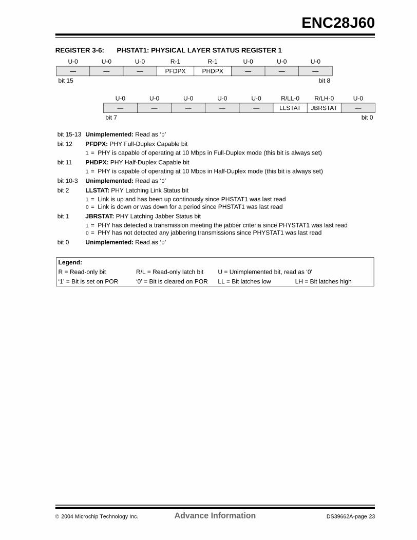
ENC28J60
REGISTER 3-6: PHSTAT1: PHYSICAL LAYER STATUS REGISTER 1
bit 15-13 Unimplemented: Read as ‘0’
bit 12 PFDPX: PHY Full-Duplex Capable bit 1 = PHY is capable of operating at 10 Mbps in Full-Duplex mode (this bit is always set)
bit 11 PHDPX: PHY Half-Duplex Capable bit1 = PHY is capable of operating at 10 Mbps in Half-Duplex mode (this bit is always set)
bit 10-3 Unimplemented: Read as ‘0’
bit 2 LLSTAT: PHY Latching Link Status bit1 = Link is up and has been up continously since PHSTAT1 was last read0 = Link is down or was down for a period since PHSTAT1 was last read
bit 1 JBRSTAT: PHY Latching Jabber Status bit
1 = PHY has detected a transmission meeting the jabber criteria since PHYSTAT1 was last read0 = PHY has not detected any jabbering transmissions since PHYSTAT1 was last read
bit 0 Unimplemented: Read as ‘0’
U-0 U-0 U-0 R-1 R-1 U-0 U-0 U-0
— — — PFDPX PHDPX — — —
bit 15 bit 8
U-0 U-0 U-0 U-0 U-0 R/LL-0 R/LH-0 U-0
— — — — — LLSTAT JBRSTAT —
bit 7 bit 0
Legend:
R = Read-only bit R/L = Read-only latch bit U = Unimplemented bit, read as ‘0’
‘1’ = Bit is set on POR ‘0’ = Bit is cleared on POR LL = Bit latches low LH = Bit latches high
2004 Microchip Technology Inc. Advance Information DS39662A-page 23

ENC28J60
REGISTER 3-7: PHSTAT2: PHYSICAL LAYER STATUS REGISTER 2
bit 15-14 Unimplemented: Read as ‘0’
bit 13 TXSTAT: PHY Transmit Status bit1 = PHY is transmitting data0 = PHY is not transmitting data
bit 12 RXSTAT: PHY Receive Status bit1 = PHY is receiving data0 = PHY is not receiving data
bit 11 COLSTAT: PHY Collision Status bit1 = A collision is occuring0 = A collision is not occuring
bit 10 LSTAT: PHY Link Status bit (non-latching)1 = Link is up0 = Link is down
bit 9 DPXSTAT: PHY Duplex Status bit(1)
1 = PHY is configured for full-duplex operation (PHCON1.PDPXMD is set)0 = PHY is configured for half-duplex operation (PHCON1.PDPXMD is clear)
Note 1: Reset values of the Duplex mode/status bits depend on the connection of the LED to the LEDBpin (see Section 2.6 “LED Configuration” for additional details).
bit 8-5 Unimplemented: Read as ‘0’
bit 4 PLRITY: Polarity Status bit1 = The polarity of the signal on TPIN+/TPIN- is reversed0 = The polarity of the signal on TPIN+/TPIN- is correct
bit 3-0 Unimplemented: Read as ‘0’
U-0 U-0 R-0 R-0 R-0 R-0 R-x U-0
— — TXSTAT RXSTAT COLSTAT LSTAT DPXSTAT(1) —
bit 15 bit 8
U-0 U-0 U-0 R-0 U-0 U-0 U-0 U-0
— — — PLRITY — — — —
bit 7 bit 0
Legend:
R = Readable bit W = Writable bit U = Unimplemented bit, read as ‘0’
-n = Value at POR ‘1’ = Bit is set ‘0’ = Bit is cleared x = Bit is unknown
DS39662A-page 24 Advance Information 2004 Microchip Technology Inc.

ENC28J60
4.0 SERIAL PERIPHERAL INTERFACE (SPI)
4.1 Overview
The ENC28J60 is designed to interface directly with theSerial Peripheral Interface (SPI) port available on manymicrocontrollers. The implementation used on thisdevice supports SPI mode 0,0 only. In addition, the SPIport requires that SCK be at Idle in a low state;selectable clock polarity is not supported.
Commands and data are sent to the device via the SIpin, with data being clocked in on the rising edge ofSCK. Data is driven out by the ENC28J60 on the SOline, on the falling edge of SCK. The CS pin must beheld low while any operation is performed and returnedhigh when finished.
FIGURE 4-1: SPI™ INPUT TIMING
FIGURE 4-2: SPI™ OUTPUT TIMING
CS
SCK
SI
SO
LSB InMSB In
High-Impedance State
CS
SCK
SO MSB Out LSB Out
Don’t CareSI
2004 Microchip Technology Inc. Advance Information DS39662A-page 25

ENC28J60
4.2 SPI Instruction Set
The operation of the ENC28J60 depends entirely oncommands given by an external host controller over theSPI interface. These commands take the form ofinstructions, of one or more bytes, which are used toaccess the control memory and Ethernet buffer spaces.At the least, instructions consist of a 3-bit opcode,
followed by a 5-bit argument that specifies either aregister address or a data constant. Write and bit fieldinstructions are also followed by one or more bytes ofdata.
A total of seven instructions are implemented on theENC28J60. Table 4-1 shows the command codes forall operations.
TABLE 4-1: SPI™ INSTRUCTION SET FOR THE ENC28J60
Instruction Name and Mnemonic
Byte 0 Byte 1 and Following
Opcode Argument Data
Read Control Register(RCR)
0 0 0 a a a a a N/A
Read Buffer Memory(RBM)
0 0 1 1 1 0 1 0 N/A
Write Control Register (WCR)
0 1 0 a a a a a d d d d d d d d
Write Buffer Memory (WBM)
0 1 1 1 1 0 1 0 d d d d d d d d
Bit Field Set(BFS)
1 0 0 a a a a a d d d d d d d d
Bit Field Clear(BFC)
1 0 1 a a a a a d d d d d d d d
System Command (Soft Reset) (SC)
1 1 1 1 1 1 1 1 N/A
Legend: a = control register address, d = data payload.
DS39662A-page 26 Advance Information 2004 Microchip Technology Inc.
ENC28J60
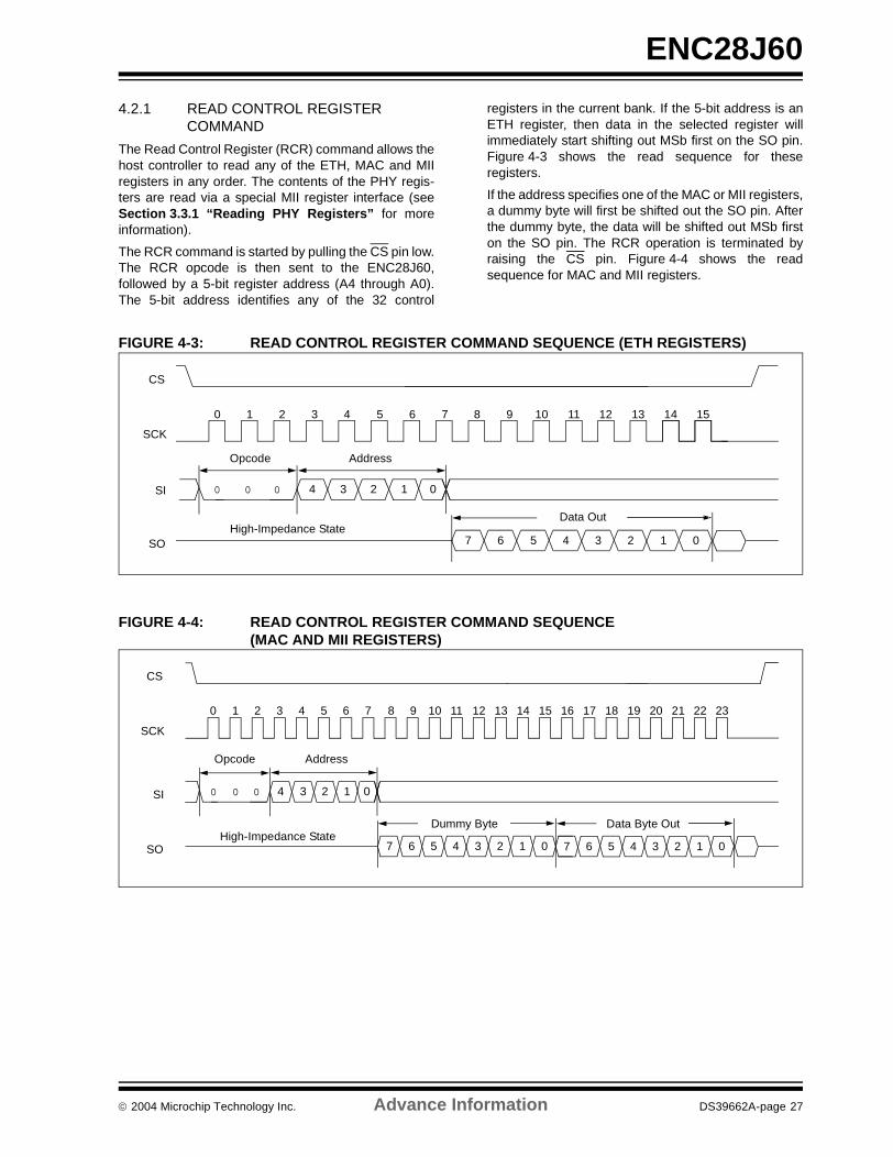
4.2.1 READ CONTROL REGISTER COMMAND
The Read Control Register (RCR) command allows thehost controller to read any of the ETH, MAC and MIIregisters in any order. The contents of the PHY regis-ters are read via a special MII register interface (seeSection 3.3.1 “Reading PHY Registers” for moreinformation).
The RCR command is started by pulling the CS pin low.The RCR opcode is then sent to the ENC28J60,followed by a 5-bit register address (A4 through A0).The 5-bit address identifies any of the 32 control
registers in the current bank. If the 5-bit address is anETH register, then data in the selected register willimmediately start shifting out MSb first on the SO pin.Figure 4-3 shows the read sequence for theseregisters.
If the address specifies one of the MAC or MII registers,a dummy byte will first be shifted out the SO pin. Afterthe dummy byte, the data will be shifted out MSb firston the SO pin. The RCR operation is terminated byraising the CS pin. Figure 4-4 shows the readsequence for MAC and MII registers.
FIGURE 4-3: READ CONTROL REGISTER COMMAND SEQUENCE (ETH REGISTERS)
FIGURE 4-4: READ CONTROL REGISTER COMMAND SEQUENCE (MAC AND MII REGISTERS)
SO
SI
SCK
CS
0 2 3 4 5 6 7 8 9 10 11 12 13 14 151
7 6 5 4 3 2 1 0
Data Out
2 034000 1
Opcode Address
High-Impedance State
SO
SI
SCK
CS
0 2 3 4 5 6 7 8 9 10 11 12 13 14 15 16 17 18 19 20 21 221
2 034000 1
7 6 5 4 3 2 1 0
Opcode
Dummy ByteHigh-Impedance State
23
7 6 5 4 3 2 1 0
Data Byte Out
Address
2004 Microchip Technology Inc. Advance Information DS39662A-page 27

ENC28J60
4.2.2 READ BUFFER MEMORY COMMAND
The Read Buffer Memory (RBM) command allows thehost controller to read bytes from the integrated 8-Kbytetransmit and receive buffer memory.
If the AUTOINC bit in the ECON2 register is set, theERDPT pointer will automatically increment to point tothe next address after the last bit of each byte is read.The next address will normally be the current addressincremented by one. However, if the last byte in thereceive buffer is read (ERDPT = ERXND), the ERDPTpointer will change to the beginning of the receivebuffer (ERXST). This allows the host controller to readpackets from the receive buffer in a continuous streamwithout keeping track of when a wraparound is needed.If AUTOINC is set when address 1FFFh is read andERXND does not point to this address, the read pointerwill increment and wrap around to 0000h.
The RBM command is started by pulling the CS pin low.The RBM opcode is then sent to the ENC28J60,followed by the 5-bit constant 1Ah. After the RBM com-mand and constant are sent, the data stored in thememory pointed to by ERDPT will be shifted out MSbfirst on the SO pin. If the host controller continues toprovide clocks on the SCK pin, without raising CS, thebyte pointed to by ERDPT will again be shifted out MSbfirst on the SO pin. In this manner, with AUTOINCenabled, it is possible to continuously read sequentialbytes from the buffer memory without any extra SPIcommand overhead. The RBM command is terminatedby raising the CS pin.
4.2.3 WRITE CONTROL REGISTER COMMAND
The Write Control Register (WCR) command allowsthe host controller to write to any of the ETH, MAC andMII Control registers in any order. The PHY registersare written to via a special MII register interface (seeSection 3.3.2 “Writing PHY Registers” for moreinformation).
The WCR command is started by pulling the CS pinlow. The WCR opcode is then sent to the ENC28J60,followed by a 5-bit address (A4 through A0). The 5-bitaddress identifies any of the 32 control registers in thecurrent bank. After the WCR command and addressare sent, actual data that is to be written is sent, MSbfirst. The data will be written to the addressed registeron the rising edge of the SCK line.
The WCR operation is terminated by raising the CS pin.If the CS line is allowed to go high before eight bits areloaded, the write will be aborted for that data byte.Refer to the timing diagram in Figure 4-5 for a moredetailed illustration of the byte write sequence.
FIGURE 4-5: WRITE CONTROL REGISTER COMMAND SEQUENCE
SO
SI
SCK
CS
0 2 3 4 5 6 7 8 9 10 11 12 13 14 151
D7 6 5 4 1 D03 2
Data Byte
High-Impedance State
2 03A4010 1
Opcode Address
DS39662A-page 28 Advance Information 2004 Microchip Technology Inc.

ENC28J60
4.2.4 WRITE BUFFER MEMORY COMMAND
The Write Buffer Memory (WBM) command allows thehost controller to write bytes to the integrated 8-Kbytetransmit and receive buffer memory.
If the AUTOINC bit in the ECON2 register is set, afterthe last bit of each byte is written, the EWRPT pointerwill automatically be incremented to point to the nextsequential address (current address + 1). If address1FFFh is written with AUTOINC set, the write pointerwill increment to 0000h.
The WBM command is started by lowering the CS pin.The WBM opcode should then be sent to theENC28J60, followed by the 5-bit constant 1Ah. Afterthe WBM command and constant are sent, the data tobe stored in the memory pointed to by EWRPT shouldbe shifted out MSb first to the ENC28J60. After 8 databits are received, the write pointer will automaticallyincrement if AUTOINC is set. The host controller cancontinue to provide clocks on the SCK pin and senddata on the SI pin, without raising CS, to keep writing tothe memory. In this manner, with AUTOINC enabled, itis possible to continuously write sequential bytes to thebuffer memory without any extra SPI commandoverhead.
The WBM command is terminated by bringing up theCS pin. Refer to Figure 4-6 for a detailed illustration ofthe write sequence.
4.2.5 BIT FIELD SET COMMAND
The Bit Field Set (BFS) command is used to set up to8 bits in any of the ETH Control registers. Note that thiscommand cannot be used on the MAC registers, MIIregisters, PHY registers or buffer memory. The BFS com-mand uses the provided data byte to perform a bit-wiseOR operation on the addressed register contents.
The BFS command is started by pulling the CS pin low.The BFS opcode is then sent, followed by a 5-bitaddress (A4 through A0). The 5-bit address identifies
any of the ETH registers in the current bank. After theBFS command and address are sent, the data bytecontaining the bit field set information should be sent,MSb first. The supplied data will be logically ORed tothe content of the addressed register on the risingedge of the SCK line for the D0 bit.
If the CS line is brought high before eight bits areloaded, the operation will be aborted for that databyte. The BFS operation is terminated by raising theCS pin.
4.2.6 BIT FIELD CLEAR COMMAND
The Bit Field Clear (BFC) command is used to clear upto 8 bits in any of the ETH Control registers. Note thatthis command cannot be used on the MAC registers,MII registers, PHY registers or buffer memory. The BFCcommand uses the provided data byte to perform a bit-wise NOTAND operation on the addressed registercontents. As an example, if a register had the contentsof F1h and the BFC command was executed with anoperand of 17h, then the register would be changed tohave the contents of E0h.
The BFC command is started by lowering the CS pin.The BFC opcode should then be sent, followed by a5-bit address (A4 through A0). The 5-bit addressidentifies any of the ETH registers in the current bank.After the BFC command and address are sent, a databyte containing the bit field clear information shouldbe sent, MSb first. The supplied data will be logicallyinverted and subsequently ANDed to the contents ofthe addressed register on the rising edge of the SCKline for the D0 bit.
The BFC operation is terminated by bringing the CSpin high. If CS is brought high before eight bits areloaded, the operation will be aborted for that databyte.
FIGURE 4-6: WRITE BUFFER MEMORY COMMAND SEQUENCE
SO
SI
SCK
CS
0 2 3 4 5 6 7 8 9 10 11 12 13 14 15 16 17 18 19 20 21 221
0 011110 7 6 5 4 1 D0 7 6 5 4 3 2 1 0
23
3 21
Data Byte 0 Data Byte 1Opcode Address
High-Impedance State
2004 Microchip Technology Inc. Advance Information DS39662A-page 29
ENC28J60
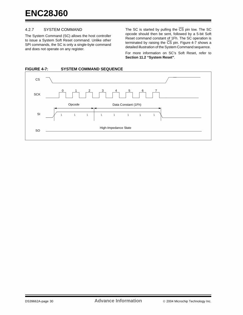
4.2.7 SYSTEM COMMAND
The System Command (SC) allows the host controllerto issue a System Soft Reset command. Unlike otherSPI commands, the SC is only a single-byte commandand does not operate on any register.
The SC is started by pulling the CS pin low. The SCopcode should then be sent, followed by a 5-bit SoftReset command constant of 1Fh. The SC operation isterminated by raising the CS pin. Figure 4-7 shows adetailed illustration of the System Command sequence.
For more information on SC’s Soft Reset, refer toSection 11.2 “System Reset”.
FIGURE 4-7: SYSTEM COMMAND SEQUENCE
SO
SI
SCK
CS
0 2 3 4 5 6 71
1 111111
Opcode
1
High-Impedance State
Data Constant (1Fh)
DS39662A-page 30 Advance Information 2004 Microchip Technology Inc.
ENC28J60
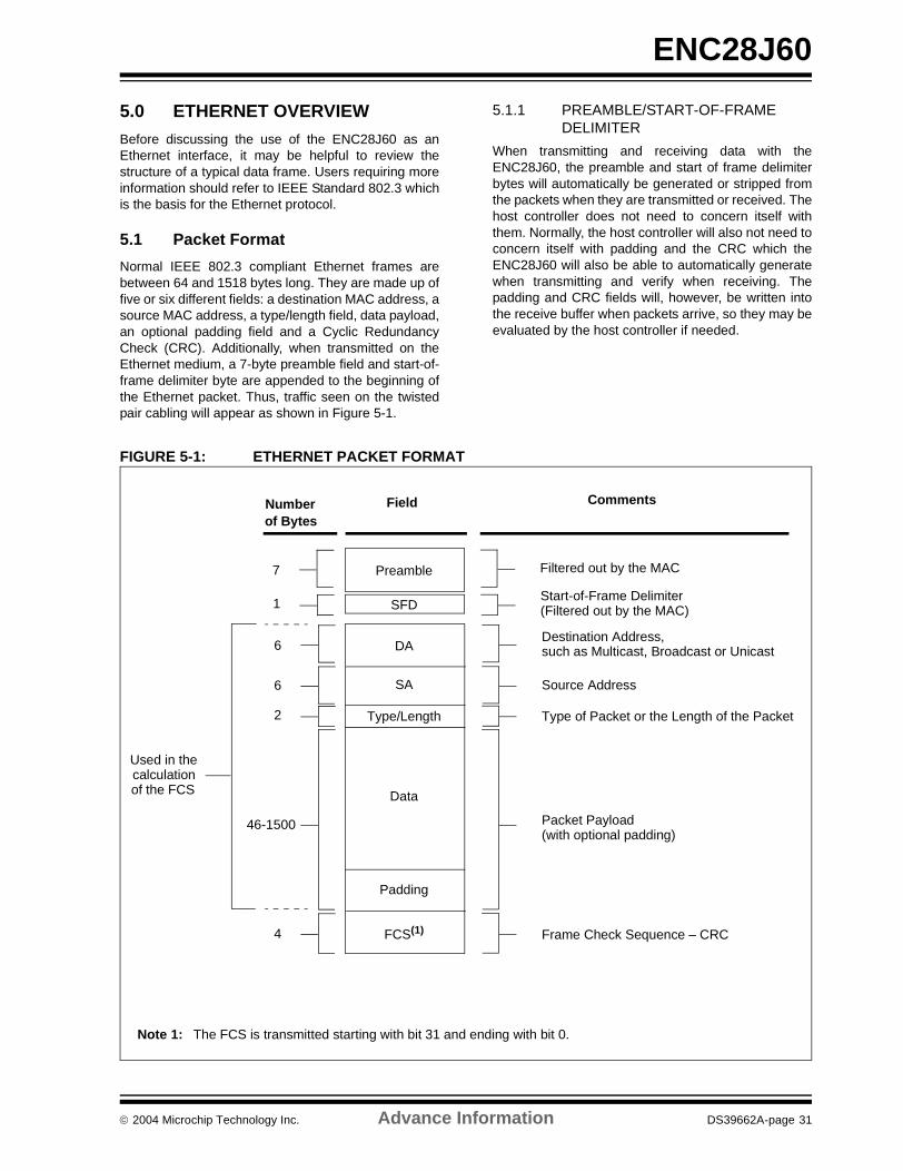
5.0 ETHERNET OVERVIEW
Before discussing the use of the ENC28J60 as anEthernet interface, it may be helpful to review thestructure of a typical data frame. Users requiring moreinformation should refer to IEEE Standard 802.3 whichis the basis for the Ethernet protocol.
5.1 Packet Format
Normal IEEE 802.3 compliant Ethernet frames arebetween 64 and 1518 bytes long. They are made up offive or six different fields: a destination MAC address, asource MAC address, a type/length field, data payload,an optional padding field and a Cyclic RedundancyCheck (CRC). Additionally, when transmitted on theEthernet medium, a 7-byte preamble field and start-of-frame delimiter byte are appended to the beginning ofthe Ethernet packet. Thus, traffic seen on the twistedpair cabling will appear as shown in Figure 5-1.
5.1.1 PREAMBLE/START-OF-FRAME DELIMITER
When transmitting and receiving data with theENC28J60, the preamble and start of frame delimiterbytes will automatically be generated or stripped fromthe packets when they are transmitted or received. Thehost controller does not need to concern itself withthem. Normally, the host controller will also not need toconcern itself with padding and the CRC which theENC28J60 will also be able to automatically generatewhen transmitting and verify when receiving. Thepadding and CRC fields will, however, be written intothe receive buffer when packets arrive, so they may beevaluated by the host controller if needed.
FIGURE 5-1: ETHERNET PACKET FORMAT
SA
Padding
FCS(1)
Number Field Comments
6
46-1500
4
DADestination Address,such as Multicast, Broadcast or Unicast
Source Address
Packet Payload
Frame Check Sequence – CRC
Type/Length
Data
of Bytes
6
2 Type of Packet or the Length of the Packet
(with optional padding)
7 Preamble Filtered out by the MAC
SFD1Start-of-Frame Delimiter(Filtered out by the MAC)
Used in the calculation
of the FCS
Note 1: The FCS is transmitted starting with bit 31 and ending with bit 0.
2004 Microchip Technology Inc. Advance Information DS39662A-page 31

ENC28J60
5.1.2 DESTINATION ADDRESS
The destination address field is a 6-byte field filled withthe MAC address of the device that the packet is directedto. If the Least Significant bit in the first byte of the MACaddress is set, the address is a multicast destination. Forexample, 01-00-00-00-F0-00 and 33-45-67-89-AB-CDare multicast addresses, while 00-00-00-00-F0-00 and32-45-67-89-AB-CD are not.
Packets with multicast destination addresses aredesigned to arrive and be important to a selected groupof Ethernet nodes. If the destination address field is thereserved multicast address, FF-FF-FF-FF-FF-FF, thepacket is a broadcast packet and it will be directed toeveryone sharing the network. If the Least Significantbit in the first byte of the MAC address is clear, theaddress is a unicast address and will be designed forusage by only the addressed node.
The ENC28J60 incorporates receive filters which canbe used to discard or accept packets with multicast,broadcast and/or unicast destination addresses. Whentransmitting packets, the host controller is responsiblefor writing the desired destination address into thetransmit buffer.
5.1.3 SOURCE ADDRESS
The source address field is a 6-byte field filled with theMAC address of the node which created the Ethernetpacket. Users of the ENC28J60 must generate aunique MAC address for each controller used.
MAC addresses consist of two portions. The first threebytes are known as the Organizationally UniqueIdentifier (OUI). OUIs are distributed by the IEEE. Thelast three bytes are address bytes at the discretion ofthe company that purchased the OUI.
When transmitting packets, the assigned source MACaddress must be written into the transmit buffer by thehost controller. The ENC28J60 will not automaticallytransmit the contents of the MAADR registers whichare used for the unicast receive filter and unicast WOLfilter.
5.1.4 TYPE/LENGTH
The type/length field is a 2-byte field which defineswhich protocol the following packet data belongs to.Alternately, if the field is filled with the contents of05DCh (1500) or any smaller number, the field isconsidered a length field and it specifies the amount ofnon-padding data which follows in the data field. Usersimplementing proprietary networks may choose to treatthis field as a length field, while applications implement-ing protocols such as the Internet Protocol (IP) orAddress Resolution Protocol (ARP), should programthis field with the appropriate type defined by theprotocol’s specification when transmitting packets.
5.1.5 DATA
The data field is a variable length field anywhere from 0to 1500 bytes. Larger data packets will violate Ethernetstandards and will be dropped by most Ethernet nodes.The ENC28J60, however, is capable of transmitting andreceiving larger packets when the Huge Frame Enablebit is set (MACON3.HFRMEN = 1).
5.1.6 PADDING
The padding field is a variable length field added tomeet IEEE 802.3 specification requirements whensmall data payloads are used. The destination, source,type, data and padding of an Ethernet packet must beno smaller than 60 bytes. Adding the required 4-byteCRC field, packets must be no smaller than 64 bytes. Ifthe data field is less than 46 bytes long, a padding fieldis required.
When transmitting packets, the ENC28J60 automaticallygenerates zero padding if the MACON3.PADCFG<2:0>bits are configured to do so. Otherwise, the host control-ler should manually add padding to the packet beforetransmitting it. The ENC28J60 will not prevent thetransmission of undersize packets should the hostcontroller command such an action.
When receiving packets, the ENC28J60 automaticallyrejects packets which are less than 18 bytes. All pack-ets 18 bytes and larger will be subject to the standardreceive filtering criteria and may be accepted as normaltraffic.
5.1.7 CRC
The CRC field is a 4-byte field which contains an indus-try standard 32-bit CRC calculated with the data fromthe destination, source, type, data and padding fields.
When receiving packets, the ENC28J60 will check theCRC of each incoming packet. If ERXFCON.CRCEN isset, packets with invalid CRCs will automatically bediscarded. If CRCEN is clear and the packet meets allother receive filtering criteria, the packet will be writteninto the receive buffer and the host controller will beable to determine if the CRC was valid by reading thereceive status vector (see Section 7.2 “ReceivingPackets”).
When transmitting packets, the ENC28J60 will auto-matically generate a valid CRC and transmit it if theMACON3.PADCFG<2:0> bits are configured to causethis. Otherwise, the host controller must generate theCRC and place it in the transmit buffer. Given the com-plexity of calculating a CRC, it is highly recommendedthat the PADCFG bits be configured such that theENC28J60 will automatically generate the CRC field.
DS39662A-page 32 Advance Information 2004 Microchip Technology Inc.
ENC28J60
6.0 INITIALIZATION
Before the ENC28J60 can be used to transmit andreceive packets, certain device settings must be initial-ized. Depending on the application, some configurationoptions may need to be changed. Normally, these tasksmay be accomplished once after Reset and do notneed to be changed thereafter.
6.1 Receive Buffer
Before receiving any packets, the receive buffer mustbe initialized by programming the ERXST and ERXNDpointers. All memory between and including theERXST and ERXND addresses will be dedicated to thereceive hardware. It is recommended that the ERXSTpointer be programmed with an even address.
Applications expecting large amounts of data andfrequent packet delivery may wish to allocate most ofthe memory as the receive buffer. Applications thatmay need to save older packets or have severalpackets ready for transmission should allocate lessmemory.
When programming the ERXST pointer, the ERXWRPTregisters will automatically be updated with the samevalues. The address in ERXWRPT will be used as thestarting location when the receive hardware begins writ-ing received data. For tracking purposes, the ERXRDPTregisters should additionally be programmed with thesame value. To program ERXRDPT, the host controllermust write to ERXRDPTL first, followed by ERXRDPTH.See Section 7.2.4 “Freeing Receive Buffer Space”for more information.
6.2 Transmission Buffer
All memory which is not used by the receive buffer isconsidered the transmission buffer. Data which is to betransmitted should be written into any unused space.After a packet is transmitted, however, the hardwarewill write a seven-byte status vector into memory afterthe last byte in the packet. Therefore, the host control-ler should leave at least seven bytes between eachpacket and the beginning of the receive buffer. Noexplicit action is required to initialize the transmissionbuffer.
6.3 Receive Filters
The appropriate receive filters should be enabled ordisabled by writing to the ERXFCON register. SeeSection 8.0 “Receive Filters” for information on howto configure it.
6.4 Waiting For OST
If the initialization procedure is being executed immedi-ately following a Power-on Reset, the ESTAT.CLKRDYbit should be polled to make certain that enough timehas elapsed before proceeding to modify the MAC andPHY registers. For more information on the OST, seeSection 2.2 “Oscillator Start-up Timer”.
2004 Microchip Technology Inc. Advance Information DS39662A-page 33

ENC28J60
6.5 MAC Initialization Settings
Several of the MAC registers require configurationduring initialization. This only needs to be done once;the order of programming is unimportant.
1. Clear the MARST bit in MACON2 to pull theMAC out of Reset.
2. Set the MARXEN bit in MACON1 to enable theMAC to receive frames. If using full duplex, mostapplications should also set TXPAUS andRXPAUS to allow IEEE defined flow control tofunction.
3. Configure the PADCFG, TXCRCEN andFULDPX bits of MACON3. Most applicationsshould enable automatic padding to at least60 bytes and always append a valid CRC. Forconvenience, many applications may wish to setthe FRMLNEN bit as well to enable frame lengthstatus reporting. The FULDPX bit should be setif the application will be connected to afull-duplex configured remote node; otherwise, itshould be left clear.
4. Configure the bits in MACON4. Manyapplications may not need to modify the Resetdefault.
5. Program the MAMXFL registers with the maxi-mum frame length to be permitted to be receivedor transmitted. Normal network nodes aredesigned to handle packets that are 1518 bytesor less.
6. Configure the Back-to-Back Inter-Packet Gapregister, MABBIPG. Most applications will pro-gram this register with 15h when Full-Duplexmode is used and 12h when Half-Duplex modeis used.
7. Configure the Non-Back-to-Back Inter-PacketGap register low byte, MAIPGL. Most applicationswill program this register with 12h.
8. If half duplex is used, the Non-Back-to-BackInter-Packet Gap register high byte, MAIPGH,should be programmed. Most applications willprogram this register to 0Ch.
9. If Half-Duplex mode is used, program theRetransmission and Collision Window registers,MACLCON1 and MACLCON2. Most applicationswill not need to change the default Reset values.If the network is spread over exceptionally longcables, the default value of MACLCON2 mayneed to be increased.
10. Program the local MAC address into theMAADR0:MAADR5 registers.
REGISTER 6-1: MACON1: MAC CONTROL REGISTER 1 U-0 U-0 U-0 R/W-0 R/W-0 R/W-0 R/W-0 R/W-0
— — — LOOPBK TXPAUS RXPAUS PASSALL MARXEN
bit 7 bit 0
bit 7-5 Unimplemented: Read as ‘0’
bit 4 LOOPBK: MAC Loopback Enable bit1 = All data transmitted by the MAC will be looped back to the MAC0 = Normal operation
bit 3 TXPAUS: Pause Control Frame Transmission Enable bit1 = Allow the MAC to transmit pause control frames (needed for flow control in full duplex)0 = Disallow pause frame transmissions
bit 2 RXPAUS: Pause Control Frame Reception Enable bit
1 = Inhibit transmissions when pause control frames are received (normal operation)0 = Ignore pause control frames which are received
bit 1 PASSALL: Pass All Received Frames Enable bit1 = Control frames received by the MAC will be wirtten into the receive buffer if not filtered out0 = Control frames will be discarded after being processed by the MAC (normal operation)
bit 0 MARXEN: MAC Receive Enable bit1 = Enable packets to be received by the MAC0 = Disable packet reception
Legend:
R = Readable bit W = Writable bit U = Unimplemented bit, read as ‘0’
-n = Value at POR ‘1’ = Bit is set ‘0’ = Bit is cleared x = Bit is unknown
DS39662A-page 34 Advance Information 2004 Microchip Technology Inc.

ENC28J60
REGISTER 6-2: MACON3: MAC CONTROL REGISTER 3 R/W-0 R/W-0 R/W-0 R/W-0 R/W-0 R/W-0 R/W-0 R/W-0
PADCFG2 PADCFG1 PADCFG0 TXCRCEN PHDRLEN HFRMEN FRMLNEN FULDPX
bit 7 bit 0
bit 7-5 PADCFG2:PACDFG0: Automatic Pad and CRC Configuration bits111 = All short frames will be zero padded to 64 bytes and a valid CRC will then be appended110 = No automatic padding of short frames101 = MAC will automatically detect VLAN Protocol frames which have a 8100h type field and
automatically pad to 64 bytes. If the frame is not a VLAN frame, it will be padded to 60 bytes. After padding, a valid CRC will be appended.
100 = No automatic padding of short frames011 = All short frames will be zero padded to 64 bytes and a valid CRC will then be appended010 = No automatic padding of short frames001 = All short frames will be zero padded to 60 bytes and a valid CRC will then be appended000 = No automatic padding of short frames
bit 4 TXCRCEN: Transmit CRC Enable bit1 = MAC will apend a valid CRC to all frames transmitted regardless of PADCFG. TXCRCEN
must be set if PADCFG specifies that a valid CRC will be appended.0 = MAC will not append a CRC. The last 4 bytes will be checked and if it is an invalid CRC, it
will be reported in the transmit status vector.
bit 3 PHDRLEN: Proprietary Header Enable bit1 = Frames presented to the MAC contain a 4-byte proprietary header which will not be used
when calculating the CRC0 = No proprietary header is present. The CRC will cover all data (normal operation).
bit 2 HFRMEN: Huge Frame Enable bit1 = Frames of any size will be allowed to be transmitted and receieved0 = Frames bigger than MAMXFL will be aborted when transmitted or received
bit 1 FRMLNEN: Frame Length Checking Enable bit1 = The type/length field of transmitted and received frames will be checked. If it represents a
length, the frame size will be compared and mismatches will be reported in thetransmit/receive status vector.
0 = Frame lengths will not be compared with the type/length field
bit 0 FULDPX: MAC Full-Duplex Enable bit1 = MAC will operate in full-duplex. PHCON1.PDPXMD must also be set.0 = MAC will operate in half-duplex. PHCON1.PDPXMD must also be clear.
Legend:
R = Readable bit W = Writable bit U = Unimplemented bit, read as ‘0’
-n = Value at POR ‘1’ = Bit is set ‘0’ = Bit is cleared x = Bit is unknown
2004 Microchip Technology Inc. Advance Information DS39662A-page 35
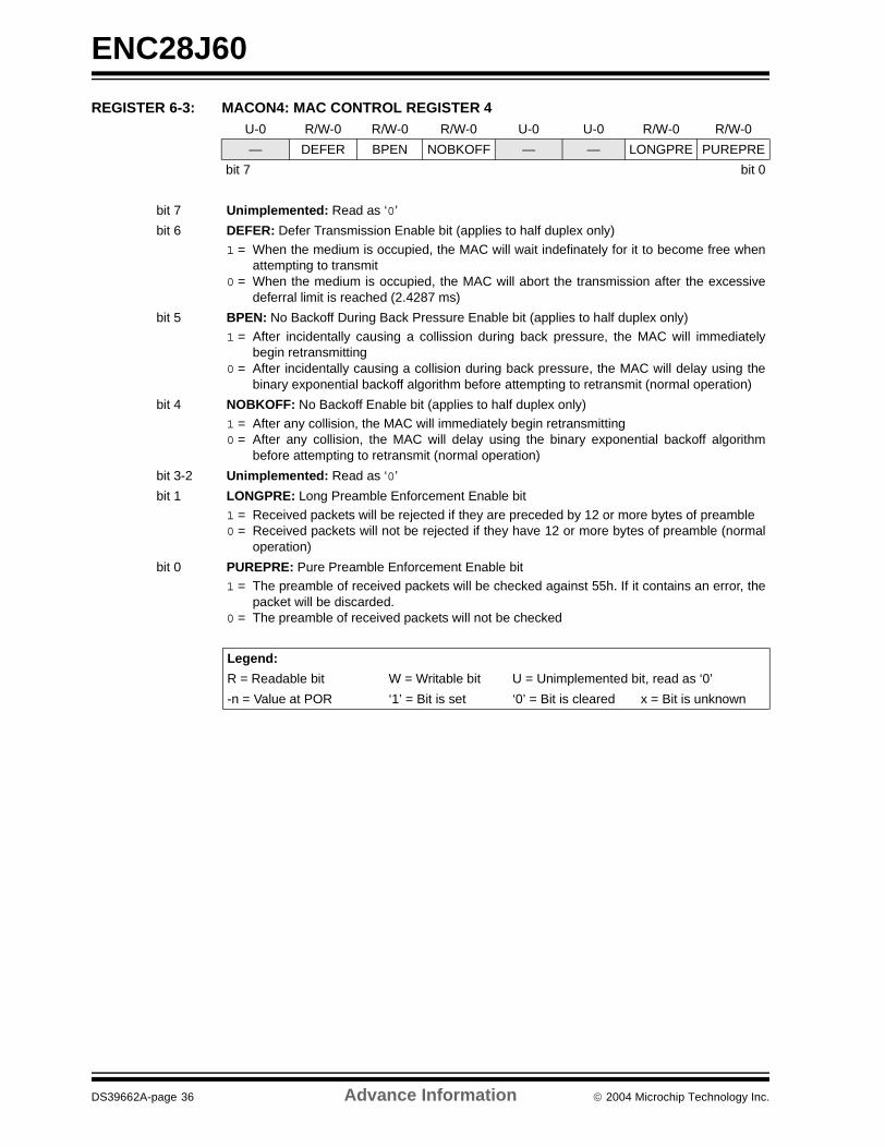
ENC28J60
REGISTER 6-3: MACON4: MAC CONTROL REGISTER 4 U-0 R/W-0 R/W-0 R/W-0 U-0 U-0 R/W-0 R/W-0
— DEFER BPEN NOBKOFF — — LONGPRE PUREPRE
bit 7 bit 0
bit 7 Unimplemented: Read as ‘0’
bit 6 DEFER: Defer Transmission Enable bit (applies to half duplex only)
1 = When the medium is occupied, the MAC will wait indefinately for it to become free whenattempting to transmit
0 = When the medium is occupied, the MAC will abort the transmission after the excessivedeferral limit is reached (2.4287 ms)
bit 5 BPEN: No Backoff During Back Pressure Enable bit (applies to half duplex only)
1 = After incidentally causing a collission during back pressure, the MAC will immediatelybegin retransmitting
0 = After incidentally causing a collision during back pressure, the MAC will delay using thebinary exponential backoff algorithm before attempting to retransmit (normal operation)
bit 4 NOBKOFF: No Backoff Enable bit (applies to half duplex only)
1 = After any collision, the MAC will immediately begin retransmitting0 = After any collision, the MAC will delay using the binary exponential backoff algorithm
before attempting to retransmit (normal operation)
bit 3-2 Unimplemented: Read as ‘0’
bit 1 LONGPRE: Long Preamble Enforcement Enable bit
1 = Received packets will be rejected if they are preceded by 12 or more bytes of preamble0 = Received packets will not be rejected if they have 12 or more bytes of preamble (normal
operation)
bit 0 PUREPRE: Pure Preamble Enforcement Enable bit1 = The preamble of received packets will be checked against 55h. If it contains an error, the
packet will be discarded.0 = The preamble of received packets will not be checked
Legend:
R = Readable bit W = Writable bit U = Unimplemented bit, read as ‘0’
-n = Value at POR ‘1’ = Bit is set ‘0’ = Bit is cleared x = Bit is unknown
DS39662A-page 36 Advance Information 2004 Microchip Technology Inc.

ENC28J60
REGISTER 6-4: MABBIPG: MAC BACK-TO-BACK INTER-PACKET GAP REGISTER U-0 R/W-0 R/W-0 R/W-0 R/W-0 R/W-0 R/W-0 R/W-0
— BBIPG6 BBIPG5 BBIPG4 BBIPG3 BBIPG2 BBIPG1 BBIPG0
bit 7 bit 0
bit 7 Unimplemented: Read as ‘0’
bit 6-0 BBIPG6:BBIPG0: Back-to-Back Inter-Packet Gap Delay Time bits
When MACON3.FULDPX = 1:Nibble time offset delay between the end of one transmission and the beginning of the next in a back-to-back sequence. The register value should be programmed to the desired period in nibble times minus 3. The recommended setting is 15h which represents the minimum IEEE specified Inter-Packet Gap (IPG) of 9.6 µs.
When MACON3.FULDPX = 0:Nibble time offset delay between the end of one transmission and the beginning of the next in a back-to-back sequence. The register value should be programmed to the desired period in nibble times minus 6. The recommended setting is 12h which represents the minimum IEEE specified Inter-Packet Gap (IPG) of 9.6 µs.
Legend:
R = Readable bit W = Writable bit U = Unimplemented bit, read as ‘0’
-n = Value at POR ‘1’ = Bit is set ‘0’ = Bit is cleared x = Bit is unknown
2004 Microchip Technology Inc. Advance Information DS39662A-page 37

ENC28J60
6.6 PHY Initialization Settings
Depending on the application, bits in three of the PHYmodule’s registers may also require configuration.
The PHCON1.PDPXMD bit partially controls thedevice’s half/full-duplex configuration. Normally, this bitis initialized correctly by the external circuitry (seeSection 2.6 “LED Configuration”). If the externalcircuitry is not present or incorrect, however, the hostcontroller must program the bit properly. Alternatively,for an externally configurable system, the PDPXMD bitmay be read and the FULDPX bit be programmed tomatch.
For proper duplex operation, the PHCON1.PDPXMDbit must also match the value of the MACON3.FULDPXbit.
If using half duplex, the host controller may wish to setthe PHCON2.HDLDIS bit to prevent automaticloopback of the data which is transmitted.
The PHY register, PHLCON, controls the outputs ofLEDA and LEDB. If an application requires a LEDconfiguration other than the default, PHLCON must bealtered to match the new requirements. The settings forLED operation are discussed in Section 2.6 “LEDConfiguration”. The PHLCON register is shown inRegister 2-2 (page 9).
REGISTER 6-5: PHCON2: PHY CONTROL REGISTER 2
bit 15 Unimplemented: Read as ‘0’
bit 14 FRCLNK: PHY Force Linkup bit
1 = Force linkup even when no link partner is detected0 = Normal operation
bit 13 TXDIS: Twisted Pair Transmitter Disable bit1 = Disable twisted pair transmitter0 = Normal operation
bit 12-11 Reserved: Write as ‘0’
bit 10 JABBER: Jabber Correction Disable bit
1 = Disable jabber correction0 = Normal operation
bit 9 Reserved: Write as ‘0’
bit 8 HDLDIS: PHY Half-Duplex Loopback Disable bitWhen PHCON1.PDPXMD = 1 or PHCON1.PLOOPBK = 1:This bit is ignored.
When PHCON1.PDPXMD = 0 and PHCON1.PLOOPBK = 0:1 = Transmitted data will only be sent out on the twisted pair interface0 = Transmitted data will be looped back to the MAC and sent out the twisted pair interface
bit 7-0 Reserved: Write as ‘0’
U-0 R/W-0 R/W-0 R/W-x R/W-x R/W-0 R/W-0 R/W-0— FRCLNK TXDIS r r JABBER r HDLDIS
bit 15
R/W-x R/W-x R/W-x R/W-x R/W-x R/W-x R/W-x R/W-x
r r r r r r r rbit 7 bit 0
Legend: r = Reserved bit
R = Readable bit W = Writable bit U = Unimplemented bit, read as ‘0’
-n = Value at POR ‘1’ = Bit is set ‘0’ = Bit is cleared x = Bit is unknown
DS39662A-page 38 Advance Information 2004 Microchip Technology Inc.

ENC28J60
7.0 TRANSMITTING AND RECEIVING PACKETS
7.1 Transmitting Packets
The MAC inside the ENC28J60 will automatically gener-ate the preamble and start-of-frame delimiter fields whentransmitting. Additionally, the MAC can generate anypadding (if needed) and the CRC if configured to do so.The host controller must generate and write all otherframe fields into the buffer memory for transmission.
Additionally, the ENC28J60 requires a single per packetcontrol byte to precede the packet for transmission. Theper packet control byte is organized as shown inFigure 7-1. Before transmitting packets, the MACregisters which alter the transmission characteristicsshould be initialized as documented in Section 6.0“Initialization”.
For an example of how the entire transmit packet andresults will look in memory, see Figure 7-2.
FIGURE 7-1: FORMAT FOR PER PACKET CONTROL BYTES
— — — — PHUGEEN PPADEN PCRCEN POVERRIDE
bit 7 bit 0
bit 7-4 Unused
bit 3 PHUGEEN: Per Packet Huge Frame Enable bit
When POVERRIDE = 1:1 = The packet will be transmitted in whole0 = The MAC will transmit up to the number of bytes specified by MAMXFL. If the packet is larger
than MAMXFL, it will be aborted after MAMXFL is reached.
When POVERRIDE = 0:
This bit is ignored.
bit 2 PPADEN: Per Packet Padding Enable bit
When POVERRIDE = 1:1 = The packet will be zero padded to 60 bytes if it is less than 60 bytes0 = The packet will be trasmitted without adding any padding bytes
When POVERRIDE = 0:This bit is ignored.
bit 1 PCRCEN: Per Packet CRC Enable bitWhen POVERRIDE = 1:1 = A valid CRC will be calculated and attached to the frame0 = No CRC will be appended. The last 4 bytes of the frame will be checked for validity as a
CRC.
When POVERRIDE = 0:This bit is ignored.
bit 0 POVERRIDE: Per Packet Override bit1 = The values of PCRCEN, PPADEN and PHUGEEN will override the configuration defined by
MACON30 = The values in MACON3 will be used to determine how the packet will be transmitted
2004 Microchip Technology Inc. Advance Information DS39662A-page 39
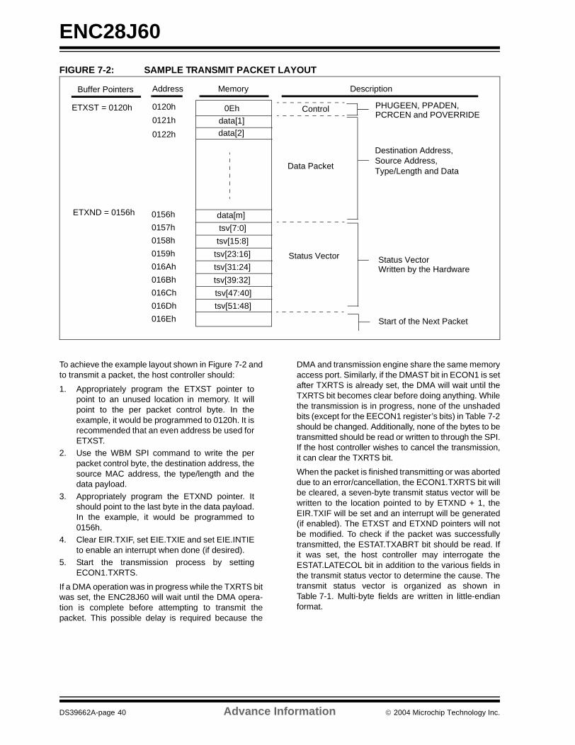
ENC28J60
FIGURE 7-2: SAMPLE TRANSMIT PACKET LAYOUT
To achieve the example layout shown in Figure 7-2 andto transmit a packet, the host controller should:
1. Appropriately program the ETXST pointer topoint to an unused location in memory. It willpoint to the per packet control byte. In theexample, it would be programmed to 0120h. It isrecommended that an even address be used forETXST.
2. Use the WBM SPI command to write the perpacket control byte, the destination address, thesource MAC address, the type/length and thedata payload.
3. Appropriately program the ETXND pointer. Itshould point to the last byte in the data payload.In the example, it would be programmed to0156h.
4. Clear EIR.TXIF, set EIE.TXIE and set EIE.INTIEto enable an interrupt when done (if desired).
5. Start the transmission process by settingECON1.TXRTS.
If a DMA operation was in progress while the TXRTS bitwas set, the ENC28J60 will wait until the DMA opera-tion is complete before attempting to transmit thepacket. This possible delay is required because the
DMA and transmission engine share the same memoryaccess port. Similarly, if the DMAST bit in ECON1 is setafter TXRTS is already set, the DMA will wait until theTXRTS bit becomes clear before doing anything. Whilethe transmission is in progress, none of the unshadedbits (except for the EECON1 register’s bits) in Table 7-2should be changed. Additionally, none of the bytes to betransmitted should be read or written to through the SPI.If the host controller wishes to cancel the transmission,it can clear the TXRTS bit.
When the packet is finished transmitting or was aborteddue to an error/cancellation, the ECON1.TXRTS bit willbe cleared, a seven-byte transmit status vector will bewritten to the location pointed to by ETXND + 1, theEIR.TXIF will be set and an interrupt will be generated(if enabled). The ETXST and ETXND pointers will notbe modified. To check if the packet was successfullytransmitted, the ESTAT.TXABRT bit should be read. Ifit was set, the host controller may interrogate theESTAT.LATECOL bit in addition to the various fields inthe transmit status vector to determine the cause. Thetransmit status vector is organized as shown inTable 7-1. Multi-byte fields are written in little-endianformat.
Control
tsv[7:0]
tsv[15:8]
Address Memory Description
0120h
0121h
0122h
016Ah
016Bh
016Ch
016Dh
0Eh PHUGEEN, PPADEN,
Destination Address,
016Eh Start of the Next Packet
tsv[23:16]
tsv[31:24]
data[1]data[2]
tsv[39:32]
tsv[47:40]
tsv[51:48]
0159h
0157h
0158h
0156h data[m]
Data Packet
Status Vector Status Vector
ETXST = 0120h
ETXND = 0156h
Type/Length and Data
PCRCEN and POVERRIDE
Written by the Hardware
Source Address,
Buffer Pointers
DS39662A-page 40 Advance Information 2004 Microchip Technology Inc.

ENC28J60
TABLE 7-1: TRANSMIT STATUS VECTORS
Bit Field Description
63-52 Zero 0
51 Transmit VLAN Tagged Frame Frame’s length/type field contained 8100h which is the VLAN protocol identifier.
50 Backpressure Applied Carrier sense method backpressure was previously applied.
49 Transmit Pause Control Frame The frame transmitted was a control frame with a valid pause opcode.
48 Transmit Control Frame The frame transmitted was a control frame.
47-32 Total Bytes Transmitted on Wire Total bytes transmitted on the wire for the current packet, including all bytes from collided attempts.
31 Transmit Underrun Reserved. This bit will always be ‘0’.
30 Transmit Giant Byte count for frame was greater than MAMXFL.
29 Transmit Late Collision Collision occurred beyond the collision window (MACLCON2).
28 Transmit Excessive Collision Packet was aborted after the number of collisions exceeded the retransmission maximum (MACLCON1).
27 Transmit Excessive Defer Packet was deferred in excess of 24,287 bit times (2.4287ms).
26 Transmit Packet Defer Packet was deferred for at least one attempt but less than an excessive defer.
25 Transmit Broadcast Packet’s destination address was a broadcast address.
24 Transmit Multicast Packet’s destination address was a multicast address.
23 Transmit Done Transmission of the packet was completed.
22 Transmit Length Out of Range Indicates that frame type/length field was larger than 1500 bytes (type field).
21 Transmit Length Check Error Indicates that frame length field value in the packet does not match the actual data byte length and is not a type field. MACON3.FRMLNEN must be set to get this error.
20 Transmit CRC Error The attached CRC in the packet did not match the internally generated CRC.
19-16 Transmit Collision Count Number of collisions the current packet incurred during transmission attempts. It applies to successfully transmitted packets and as such, will not show the possible maximum count of 16 collisions.
15-0 Transmit Byte Count Total bytes in frame not counting collided bytes.
2004 Microchip Technology Inc. Advance Information DS39662A-page 41

ENC28J60
TABLE 7-2: SUMMARY OF REGISTERS USED FOR PACKET TRANSMISSION
Register Name
Bit 7 Bit 6 Bit 5 Bit 4 Bit 3 Bit 2 Bit 1 Bit 0Reset Values
on page
EIE INTIE PKTIE DMAIE LINKIE TXIE WOLIE TXERIE RXERIE 13
EIR — PKTIF DMAIF LINKIF TXIF WOLIF TXERIF RXERIF 13
ESTAT INT r r LATECOL — RXBUSY TXABRT CLKRDY 13
ECON1 TXRST RXRST DMAST CSUMEN TXRTS RXEN BSEL1 BSEL0 13
ETXSTL TX Start Low Byte (ETXST<7:0>) 13
ETXSTH — — — TX Start High Byte (ETXST<12:8>) 13
ETXNDL TX End Low Byte (ETXND<7:0>) 13
ETXNDH — — — TX End High Byte (ETXND<12:8>) 13
MACON1 — — — LOOPBK TXPAUS RXPAUS PASSALL MARXEN 14
MACON2 MARST RNDRST — — MARXRST RFUNRST MATXRST TFUNRST 14
MACON3 PADCFG2 PADCFG1 PADCFG0 TXCRCEN PHDRLEN HFRMEN FRMLNEN FULDPX 14
MACON4 — DEFER BPEN NOBKOFF — — LONGPRE PUREPRE 14
MABBIPG — Back-to-Back Inter-Packet Gap (BBIPG<6:0>) 14
MAIPGL — Non-Back-to-Back Inter-Packet Gap Low Byte (MAIPGL<6:0>) 14
MAIPGH — Non-Back-to-Back Inter-Packet Gap High Byte (MAIPGH<6:0>) 14
MACLCON1 — — — — Retransmission Maximum (RETMAX<3:0>) 14
MACLCON2 — — Collision Window (COLWIN<5:0>) 14
MAMXFLL Maximum Frame Length Low Byte (MAMXFL<7:0>) 14
MAMXFLH Maximum Frame Length High Byte (MAMXFL<15:8>) 14
MAPHSUP r — — r RSTRMII — — r 14
Legend: — = unimplemented, r = reserved bit. Shaded cells are not used.
DS39662A-page 42 Advance Information 2004 Microchip Technology Inc.

ENC28J60
7.2 Receiving Packets
7.2.1 ENABLING RECEPTION
Assuming that the receive buffer has been initialized,the MAC has been properly configured and the receivefilters have been configured to receive Ethernetpackets, the host controller should:
1. If an interrupt is desired whenever a packet isreceived, set EIE.PKTIE and EIE.INTIE.
2. If an interrupt is desired whenever a packet isdropped due to insufficient buffer space, clearEIR.RXERIF and set both EIE.RXERIE andEIE.INTIE
3. Enable reception by setting ECON1.RXEN.
After setting RXEN, the Duplex mode and the receivebuffer start and end pointers should not be modified.Additionally, to prevent unexpected packets from arriv-ing, it is recommended that RXEN be cleared beforealtering the receive filter configuration (ERXFCON) andMAC address.
After reception is enabled, packets which are notfiltered out will be written into the circular receive buffer.Any packet which does not meet the necessary filtercriteria will be discarded and the host controller will nothave any means of identifying that a packet was thrownaway. When a packet is accepted and completelywritten into the buffer, the EPKTCNT register will incre-ment, the EIR.PKTIF bit will be set, an interrupt will begenerated (if enabled) and the hardware write pointer,ERXWRPT, will automatically advance.
7.2.2 RECEIVE PACKET LAYOUT
Figure 7-3 shows the layout of a received packet. Thepackets are preceded by a six-byte header whichcontains a next packet pointer, in addition to a receivestatus vector which contains receive statistics, includ-ing the packet’s size. This receive status vector isshown in Table 7-3.
If the last byte in the packet ends on an odd valueaddress, the hardware will automatically add a paddingbyte when advancing the hardware write pointer. Assuch, all packets will start on an even boundary.
FIGURE 7-3: SAMPLE RECEIVE PACKET LAYOUT
Low ByteHigh Byte
rsv[7:0]rsv[15:8]
data[m – 3]
data[m – 2]
data[m – 1]
data[m]
Address Memory Description
1020h
1021h
1022h
1023h
106Ah
106Bh
106Ch
1059h
10h6Eh
Next Packet Pointer
Packet Data: destination address,
Receive Status Vector
crc[31:24]
crc[23:16]
crc[15:8]
crc[7:0]
106Eh Start of the Next Packet
rsv[23:16]
rsv[30:24]1024h
1025hdata[1]1026hdata[2]1027h
status[7:0]
status[15:8]
status[23:16]
status[31:24]
106DhByte Skipped to EnsureEven Buffer Address
101FhEnd of the Previous Packet
Packet N
Packet N + 1
Packet N + 2
source address, type/length, data,padding, CRC
2004 Microchip Technology Inc. Advance Information DS39662A-page 43
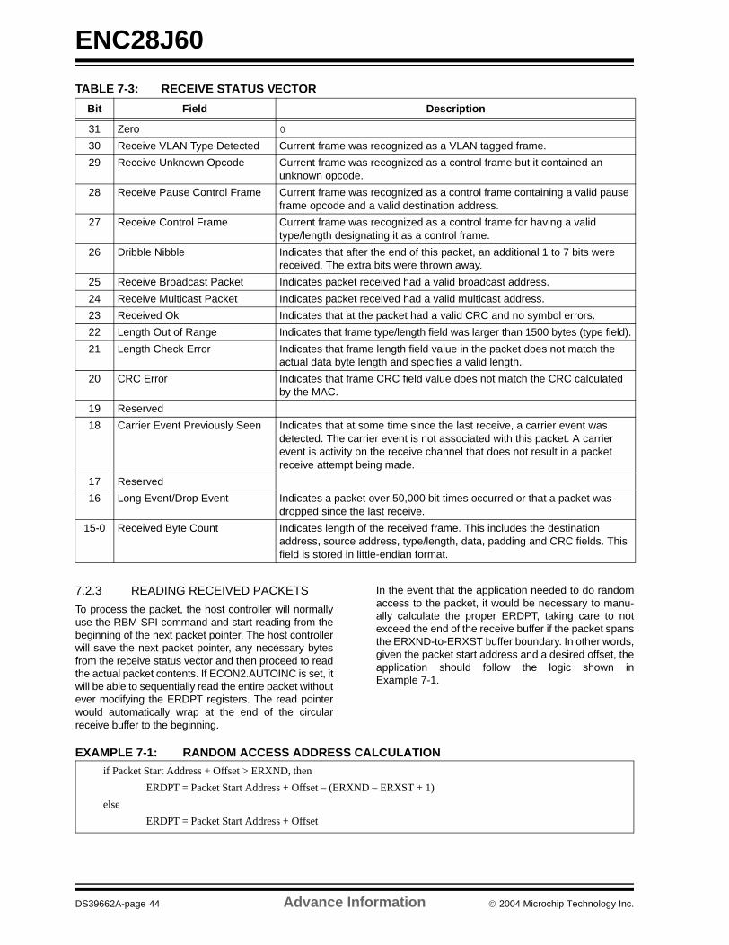
ENC28J60
TABLE 7-3: RECEIVE STATUS VECTOR
7.2.3 READING RECEIVED PACKETS
To process the packet, the host controller will normallyuse the RBM SPI command and start reading from thebeginning of the next packet pointer. The host controllerwill save the next packet pointer, any necessary bytesfrom the receive status vector and then proceed to readthe actual packet contents. If ECON2.AUTOINC is set, itwill be able to sequentially read the entire packet withoutever modifying the ERDPT registers. The read pointerwould automatically wrap at the end of the circularreceive buffer to the beginning.
In the event that the application needed to do randomaccess to the packet, it would be necessary to manu-ally calculate the proper ERDPT, taking care to notexceed the end of the receive buffer if the packet spansthe ERXND-to-ERXST buffer boundary. In other words,given the packet start address and a desired offset, theapplication should follow the logic shown inExample 7-1.
EXAMPLE 7-1: RANDOM ACCESS ADDRESS CALCULATION
Bit Field Description
31 Zero 0
30 Receive VLAN Type Detected Current frame was recognized as a VLAN tagged frame.
29 Receive Unknown Opcode Current frame was recognized as a control frame but it contained an unknown opcode.
28 Receive Pause Control Frame Current frame was recognized as a control frame containing a valid pause frame opcode and a valid destination address.
27 Receive Control Frame Current frame was recognized as a control frame for having a valid type/length designating it as a control frame.
26 Dribble Nibble Indicates that after the end of this packet, an additional 1 to 7 bits were received. The extra bits were thrown away.
25 Receive Broadcast Packet Indicates packet received had a valid broadcast address.
24 Receive Multicast Packet Indicates packet received had a valid multicast address.
23 Received Ok Indicates that at the packet had a valid CRC and no symbol errors.
22 Length Out of Range Indicates that frame type/length field was larger than 1500 bytes (type field).
21 Length Check Error Indicates that frame length field value in the packet does not match the actual data byte length and specifies a valid length.
20 CRC Error Indicates that frame CRC field value does not match the CRC calculated by the MAC.
19 Reserved
18 Carrier Event Previously Seen Indicates that at some time since the last receive, a carrier event was detected. The carrier event is not associated with this packet. A carrier event is activity on the receive channel that does not result in a packet receive attempt being made.
17 Reserved
16 Long Event/Drop Event Indicates a packet over 50,000 bit times occurred or that a packet was dropped since the last receive.
15-0 Received Byte Count Indicates length of the received frame. This includes the destination address, source address, type/length, data, padding and CRC fields. This field is stored in little-endian format.
if Packet Start Address + Offset > ERXND, then
ERDPT = Packet Start Address + Offset – (ERXND – ERXST + 1)
else
ERDPT = Packet Start Address + Offset
DS39662A-page 44 Advance Information 2004 Microchip Technology Inc.

ENC28J60
7.2.4 FREEING RECEIVE BUFFER SPACE
After the host controller has processed a packet (or partof the packet) and wishes to free the buffer space usedby the processed data, the host controller mustadvance the receive buffer read pointer, ERXRDPT.The ENC28J60 will always write up to, but not includ-ing, the memory pointed to by the receive buffer readpointer. If the ENC28J60 ever attempts to overwrite thereceive buffer read pointer location, the packet inprogress will be aborted, the EIR.RXERIF will be setand an interrupt will be generated (if enabled). In thismanner, the hardware will never overwrite unproc-essed packets. Normally, the ERXRDPT will beadvanced to the value pointed to by the next packetpointer which precedes the receive status vector for thecurrent packet. Following such a procedure will notrequire any pointer calculations to account for wrappingat the end of the circular receive buffer.
The receive buffer read pointer low byte (ERXRDPTLregister) is internally buffered to prevent the pointerfrom moving when only one byte is updated through theSPI. To move ERXRDPT, the host controller must writeto ERXRDPTL first. The write will update the internalbuffer but will not affect the register. When the hostcontroller writes to ERXRDPTH, the internally bufferedlow byte will be loaded into the ERXRDPTL register atthe same time. The ERXRDPT bytes can be read inany order. When they are read, the actual value of theregisters will be returned. As a result, the buffered lowbyte is not readable.
In addition to advancing the receive buffer read pointer,after each packet is fully processed, the host controllermust write a ‘1’ to the ECON2.PKTDEC bit. Doing sowill cause the EPKTCNT register to decrement by 1.After decrementing, if EPKTCNT is ‘0’, the EIR.PKTIFflag will automatically be cleared. Otherwise, it willremain set, indicating that additional packets are in thereceive buffer and are waiting to be processed.Attempts to decrement EPKTCNT below 0 are ignored.Additionally, if the EPKTCNT register ever maximizesat 255, all new packets which are received will beaborted, even if buffer space is available. To indicatethe error, the EIR.RXERIF will be set and an interruptwill be generated (if enabled). To prevent this condition,the host controller must properly decrement thecounter whenever a packet is processed.
Because only one pointer is available to control bufferarea ownership, the host controller must process pack-ets in the order they are received. If the host controllerwishes to save a packet to be processed later, it shouldcopy the packet to an unused location in memory. Itmay accomplish this efficiently using the integratedDMA controller (see Section 13.0 “Direct MemoryAccess Controller”).
7.2.5 RECEIVE BUFFER FREE SPACE
At any time the host controller wishes to know howmuch receive buffer space is remaining, it should readthe hardware write pointer (ERXWRPT registers) andcompare it with the ERXRDPT registers. Combinedwith the known size of the receive buffer, the free spacecan be derived.
When reading the ERXWRPT register with the receivehardware enabled, special care must be taken toensure the low and high bytes are read as a matchingset.
To be assured that a matching set is obtained:
1. Read the EPKTCNT register and save itscontents.
2. Read ERXWRPTL and ERXWRPTH.
3. Read the EPKTCNT register again. 4. Compare the two packet counts. If they are not
the same, go back to step 2.
With the hardware write pointer obtained, the freespace can be calculated as shown in Example 7-2. Thehardware prohibits moving the write pointer to thesame value occupied by ERXRDPT (except when thebuffer pointers are being configured), so at least onebyte will always go unused in the buffer. The examplecalculation reflects the lost byte.
EXAMPLE 7-2: RECEIVE BUFFER FREE SPACE CALCULATION
Note: The ERXWRPT registers only updatewhen a packet has been successfullyreceived. If the host controller reads it justbefore another packet is to be successfullycompleted, the value returned could bestale and off by the maximum frame lengthpermitted (MAMXFLN) plus 7. Further-more, as the host controller reads onebyte of ERXWRPT, a new packet mayarrive and update the pointer before thehost controller has an opportunity to readthe other byte of ERXWRPT.
if ERXWRPT > ERXRDPT, then
Free Space = (ERXND – ERXST) – (ERXWRPT – ERXRDPT)
else if ERXWRPT = ERXRDPT, then
Free Space = (ERXND – ERXST)
else
Free Space = ERXRDPT – ERXWRPT – 1
2004 Microchip Technology Inc. Advance Information DS39662A-page 45
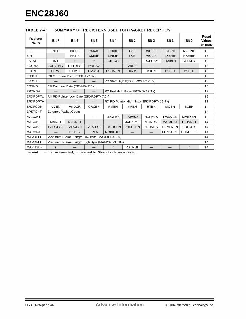
ENC28J60
TABLE 7-4: SUMMARY OF REGISTERS USED FOR PACKET RECEPTION
Register Name
Bit 7 Bit 6 Bit 5 Bit 4 Bit 3 Bit 2 Bit 1 Bit 0Reset Values
on page
EIE INTIE PKTIE DMAIE LINKIE TXIE WOLIE TXERIE RXERIE 13
EIR — PKTIF DMAIF LINKIF TXIF WOLIF TXERIF RXERIF 13
ESTAT INT r r LATECOL — RXBUSY TXABRT CLKRDY 13
ECON2 AUTOINC PKTDEC PWRSV — VRPS — — — 13
ECON1 TXRST RXRST DMAST CSUMEN TXRTS RXEN BSEL1 BSEL0 13
ERXSTL RX Start Low Byte (ERXST<7:0>) 13
ERXSTH — — — RX Start High Byte (ERXST<12:8>) 13
ERXNDL RX End Low Byte (ERXND<7:0>) 13
ERXNDH — — — RX End High Byte (ERXND<12:8>) 13
ERXRDPTL RX RD Pointer Low Byte (ERXRDPT<7:0>) 13
ERXRDPTH — — — RX RD Pointer High Byte (ERXRDPT<12:8>) 13
ERXFCON UCEN ANDOR CRCEN PMEN MPEN HTEN MCEN BCEN 14
EPKTCNT Ethernet Packet Count 14
MACON1 — — — LOOPBK TXPAUS RXPAUS PASSALL MARXEN 14
MACON2 MARST RNDRST — — MARXRST RFUNRST MATXRST TFUNRST 14
MACON3 PADCFG2 PADCFG1 PADCFG0 TXCRCEN PHDRLEN HFRMEN FRMLNEN FULDPX 14
MACON4 — DEFER BPEN NOBKOFF — — LONGPRE PUREPRE 14
MAMXFLL Maximum Frame Length Low Byte (MAMXFL<7:0>) 14
MAMXFLH Maximum Frame Length High Byte (MAMXFL<15:8>) 14
MAPHSUP r — — r RSTRMII — — r 14
Legend: — = unimplemented, r = reserved bit. Shaded cells are not used.
DS39662A-page 46 Advance Information 2004 Microchip Technology Inc.

ENC28J60
8.0 RECEIVE FILTERS
To minimize the processing requirements of the hostcontroller, the ENC28J60 incorporates several differentreceive filters which can automatically reject packetswhich are not needed. Six different types of packetfilters are implemented:
• Unicast
• Pattern Match• Magic Packet™• Hash Table
• Multicast• Broadcast
The individual filters are all configured by the ERXFCONregister (Register 8-1). More than one filter can be activeat any given time. Additionally, the filters can be config-ured by the ANDOR bit to either logically AND, orlogically OR, the tests of several filters. In other words,the filters may be set so that only packets accepted byall active filters are accepted, or a packet accepted byany one filter is accepted. The flowcharts in Figure 8-1and Figure 8-2 show the effect that each of the filters willhave depending on the setting of ANDOR.
The device can enter Promiscuous mode and receiveall packets by clearing the ERXFCON register. Theproper setting of the register will depend on theapplication requirements.
2004 Microchip Technology Inc. Advance Information DS39662A-page 47

ENC28J60
REGISTER 8-1: ERXFCON: RECEIVE FILTER CONTROL REGISTER R/W-1 R/W-0 R/W-1 R/W-0 R/W-0 R/W-0 R/W-0 R/W-1
UCEN ANDOR CRCEN PMEN MPEN HTEN MCEN BCEN
bit 7 bit 0
bit 7 UCEN: Unicast Filter Enable bitWhen ANDOR = 1:1 = Packets not having a destination address matching the local MAC address will be discarded0 = Filter disabledWhen ANDOR = 0:1 = Packets with a destination address matching the local MAC address will be accepted0 = Filter disabled
bit 6 ANDOR: AND/OR Filter Select bit1 = AND: Packets will be rejected unless all enabled filters accept the packet0 = OR: Packets will be accepted unless all enabled filters reject the packet
bit 5 CRCEN: Post-Filter CRC Check Enable bit1 = All packets with an invalid CRC will be discarded0 = The CRC validity will be ignored
bit 4 PMEN: Pattern Match Filter Enable bitWhen ANDOR = 1:1 = Packets must meet the pattern match criteria or they will be discarded0 = Filter disabledWhen ANDOR = 0:1 = Packets which meet the pattern match criteria will be accepted0 = Filter disabled
bit 3 MPEN: Magic Packet Filter Enable bitWhen ANDOR = 1:1 = Packets must be Magic Packets for the local MAC address or they will be discarded0 = Filter disabledWhen ANDOR = 0:1 = Magic Packets for the local MAC address will be accepted0 = Filter disabled
bit 2 HTEN: Hash Table Filter Enable bitWhen ANDOR = 1:1 = Packets must meet the hash table criteria or they will be discarded0 = Filter disabledWhen ANDOR = 0:1 = Packets which meet the hash table criteria will be accepted0 = Filter disabled
bit 1 MCEN: Multicast Filter Enable bitWhen ANDOR = 1:1 = Packets must have the Least Significant bit set in the destination address or they will be discarded0 = Filter disabledWhen ANDOR = 0:1 = Packets which have the Least Significant bit set in the destination address will be accepted0 = Filter disabled
bit 0 BCEN: Broadcast Filter Enable bitWhen ANDOR = 1:1 = Packets must have a destination address of FF-FF-FF-FF-FF-FF or they will be discarded0 = Filter disabledWhen ANDOR = 0:1 = Packets which have a destination address of FF-FF-FF-FF-FF-FF will be accepted0 = Filter disabled
Legend:
R = Readable bit W = Writable bit U = Unimplemented bit, read as ‘0’
- n = Value at POR ‘1’ = Bit is set ‘0’ = Bit is cleared x = Bit is unknown
DS39662A-page 48 Advance Information 2004 Microchip Technology Inc.
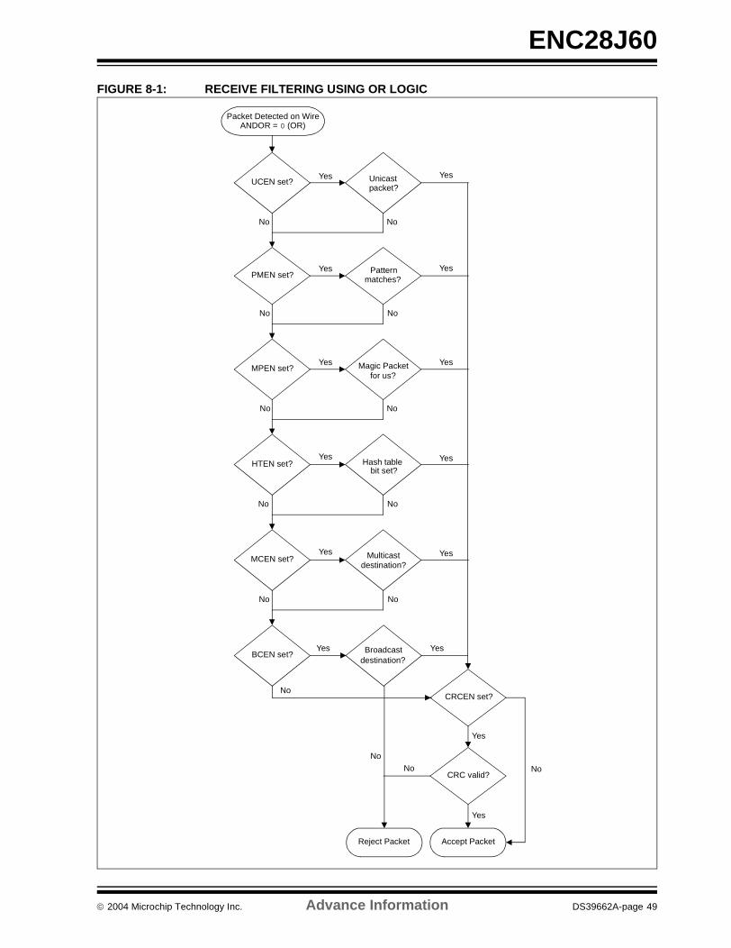
ENC28J60
FIGURE 8-1: RECEIVE FILTERING USING OR LOGIC
CRCEN set?
Packet Detected on WireANDOR = 0 (OR)
CRC valid?
Yes
Yes
Accept PacketReject Packet
No
UCEN set?
PMEN set?
MPEN set?
HTEN set?
MCEN set?
BCEN set?
No
No
No
No
No
Unicast
Pattern
Magic Packet
Hash table
Multicast
Broadcastdestination?
Yes
Yes
Yes
Yes
Yes
Yes
No
No
No
No
No
No
Yes
Yes
Yes
Yes
Yes
Yes
No
packet?
matches?
for us?
bit set?
destination?
No
2004 Microchip Technology Inc. Advance Information DS39662A-page 49
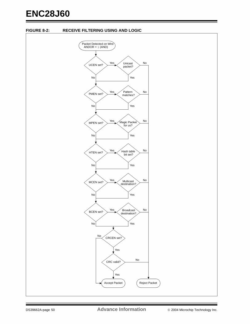
ENC28J60
FIGURE 8-2: RECEIVE FILTERING USING AND LOGIC
CRCEN set?
Packet Detected on WireANDOR = 1 (AND)
CRC valid?
Yes
Yes
Accept Packet Reject Packet
UCEN set?
PMEN set?
MPEN set?
HTEN set?
MCEN set?
BCEN set?
No
Unicast
Pattern
Magic Packet
Hash table
Multicast
Broadcastdestination?
Yes
Yes
Yes
Yes
Yes
Yes
No
No
No
No
No
No
No Yes
No
No
Yes
No Yes
No Yes
No Yes
No Yes
destination?
bit set?
for us?
matches?
packet?
DS39662A-page 50 Advance Information 2004 Microchip Technology Inc.

ENC28J60
8.1 Unicast Filter
The unicast receive filter checks the destinationaddress of all incoming packets. If the destinationaddress exactly matches the contents of the MAADRregisters, the packet will meet the unicast filter criteria.
8.2 Pattern Match Filter
The pattern match filter selects up to 64 bytes from theincoming packet and calculates an IP checksum of thebytes. The checksum is then compared to the EPMCSregisters. The packet meets the pattern match filtercriteria if the calculated checksum matches the EPMCSregisters. The pattern match filter may be useful forfiltering packets which have expected data inside them.
To use the pattern match filter, the host controller mustprogram the pattern match offset (EPMOH:EPMOL), allof the pattern match mask bytes (EPMM7:EPMM0) andthe pattern match checksum resister pair(EPMCSH:EPMCSL). The pattern match offset shouldbe loaded with the offset from the beginning of the des-tination address field to the 64-byte window which willbe used for the checksum computation. Within the64-byte window, each individual byte can be selectivelyincluded or excluded from the checksum computationby setting or clearing the respective bit in the patternmatch mask. If a packet is received which would causethe 64 byte window to extend past the end of the CRC,
the filter criteria will immediately not be met, even if thecorresponding mask bits are all ‘0’. The pattern matchchecksum registers should be programmed to thechecksum which is expected for the selected bytes.The checksum is calculated in the same manner thatthe DMA module calculates checksums (seeSection 13.2 “Checksum Calculations”). Data byteswhich have corresponding mask bits programmed to ‘0’are completely removed for purposes of calculating thechecksum, as opposed to treating the data bytes aszero.
As an example, if the application wished to filter allpackets having a particular source MAC address of00-04-A3-FF-FF-FF, it could program the pattern matchoffset to 0000h and then set bits 6 and 7 of EPMM0 andbits 0, 1, 2 and 3 of EPMM1 (assuming all other maskbits are ‘0’). The proper checksum to program into theEPMCS registers would be 0x5BFC. As an alternativeconfiguration, it could program the offset to 0006h andset bits 0, 1, 2, 3, 4 and 5 of EPMM0. The checksumwould still be 5BFCh. However, the second case wouldbe less desirable as packets less than 70 bytes longcould never meet the pattern match criteria, even ifthey would generate the proper checksum given themask configuration.
Another example of a pattern matching filter isillustrated in Figure 8-3.
FIGURE 8-3: SAMPLE PATTERN MATCHING FORMAT
SA
EMPOH:EPMOL = 0006h
FCSDA Type/Length Data
Bytes used forChecksum Computation
EPPM7:EMPPM0 = 0000000000001F0Ah
11 22 33 44 55 66 77 88 99 AA BB CC 00 5A 09 0A 0B 0C 0D . . . 40 . . . FE 45 23 01ReceivedData
Field
0 1 2 3 4 5 6 7 8 9 10 11 12 13 14 15 16 17 18 . . . 70 . . .Byte #
64-Byte Window usedfor Pattern Matching
Input Configuration:
Values used for Checksum Computation = 88h, AAh, 09h, 0Ah, 0Bh, 0Ch, 0Dh, 00h
EPMCSH:EPMCSL = 563Fh
Note: Received data is shown in hexadecimal. Byte numbers are shown in decimal format.
(00h padding byte added by hardware)
2004 Microchip Technology Inc. Advance Information DS39662A-page 51

ENC28J60
8.3 Magic Packet™ Filter
The Magic Packet filter checks the destination addressand data fields of all incoming packets. If the destinationaddress matches the MAADR registers and the datafield holds a valid Magic Packet pattern someplace
within it, then the packet will meet the Magic Packet filtercriteria. The Magic Packet pattern consists of a syncpattern of six 0xFF bytes, followed by 16 repeats of thedestination address. See Figure 8-4 for a sample MagicPacket.
FIGURE 8-4: SAMPLE MAGIC PACKET™
8.4 Hash Table Filter
The hash table receive filter performs a CRC over thesix destination address bytes in the packet. The CRC isthen used as a pointer into the bits of the EHT registers.If the pointer points to a bit which is set, the packetmeets the hash table filter criteria. For example, if theCRC is calculated to be 0x5, bit 5 in the hash table willbe checked. If it is set, the hash table filter criteria willbe met. If every bit is clear in the hash table, the filtercriteria will never be met. Similarly, if every bit is set inthe hash table, the filter criteria will always be met.
8.5 Multicast Filter
The multicast receive filter checks the destinationaddress of all incoming packets. If the Least Significantbit of the first byte of the destination address is set, thepacket will meet the multicast filter criteria.
8.6 Broadcast Filter
The broadcast receive filter checks the destinationaddress of all incoming packets. If the destinationaddress is FF-FF-FF-FF-FF-FF, the packet will meetthe broadcast filter criteria.
SA
FCS
DA
Type/Length
Data
11 22 33 44 55 66
00 FE
09 0A 0B 0C 0D 0E
ReceivedData Field
77 88 99 AA BB CC
EF 54 32 10
FF FF FF FF FF 00
FF FF FF FF FF FF
11 22 33 44 55 66
11 22 33 44 55 66
11 22 33 44 55 66
11 22 33 44 55 66
11 22 33 44 55 66
11 22 33 44 55 66
11 22 33 44 55 66
11 22 33 44 55 66
11 22 33 44 55 66
11 22 33 44 55 66
11 22 33 44 55 66
11 22 33 44 55 66
11 22 33 44 55 66
11 22 33 44 55 66
11 22 33 44 55 66
11 22 33 44 55 66
19 1A 1B 1C 1D 1E
Data
Sync Pattern
Sixteen Repeats ofthe Station Address
Comments
DS39662A-page 52 Advance Information 2004 Microchip Technology Inc.

ENC28J60
9.0 DUPLEX MODE CONFIGURATION AND NEGOTIATION
The ENC28J60 does not support automatic duplexnegotiation. If it is connected to an automatic duplexnegotiation enabled network switch or Ethernet control-ler, the ENC28J60 will be detected as a half-duplexdevice. To communicate in Full-Duplex mode, theENC28J60 and the remote node (switch, router orEthernet controller) must be manually configured forfull-duplex operation.
9.1 Half-Duplex Operation
The ENC28J60 operates in Half-Duplex mode whenMACON3.FULDPX = 0 and PHCON1.PDPXMD = 0. Ifonly one of these two bits is set, the ENC28J60 will bein an indeterminate state and not function correctly.Since switching between Full and Half-Duplex modesmay result in this indeterminate state, the host control-ler should not transmit any packets (maintainECON1.TXRTS clear) and packet reception should bedisabled (ECON1.RXEN and ESTAT.RXBUSY shouldbe clear) during this period.
In Half-Duplex mode, only one Ethernet controller maybe transmitting on the physical medium at any time. Ifthe host controller sets the ECON1.TXRTS bit,requesting that a packet be transmitted while anotherEthernet controller is already transmitting, theENC28J60 will delay, waiting for the remote transmitterto stop. After the transmission stops, the ENC28J60will attempt to transmit its packet. If another Ethernetcontroller starts transmitting at approximately the sametime that the ENC28J60 starts transmitting, the data onthe wire will become corrupt and a collision will occur.The hardware will handle this condition in one of twoways:
1. If the collision occurs before the number of bytesspecified by the “Collision Window” inMACLCON2 were transmitted, theECON1.TXRTS bit will remain set, a randomexponential back off delay will elapse as definedby the IEEE 802.3 specification and then a newattempt to transmit the packet from the begin-ning will occur. The host controller will not needto intervene. If the number of retransmissionattempts already matches the “RetransmissionMaximum” (RETMAX) defined in MACLCON1,the packet will be aborted and ECON1.TXRTSwill be cleared. The host controller will then beresponsible for taking appropriate action. Thehost controller will be able to determine that thepacket was aborted instead of being success-fully transmitted by reading the ESTAT.TXABRTflag. For more information, see Section 7.1“Transmitting Packets”. A transmit abort willcause the transmit error interrupt.
2. If the collision occurs after the number of bytesspecified by the “Collision Window” inMACLCON2 were transmitted, the packet will beimmediately aborted without any retransmissionattempts. Ordinarily, in 802.3 compliantnetworks which are properly configured, this latecollision will not occur. User intervention may berequired to correct the issue. This problem mayoccur as a result of a full-duplex node attemptingto transmit on the half-duplex medium. Alter-nately, the ENC28J60 may be attempting tooperate in Half-Duplex mode while it may beconnected to a full-duplex network. Excessivelylong cabling and network size may also be apossible cause of late collisions.
When set in Half-Duplex mode, the Reset defaultconfiguration will loop transmitted packets back toitself. Unless the receive filter configuration filters thesepackets out, they will be written into the circular receivebuffer, just as any other network traffic. To stop thisbehavior, the host controller should set thePHCON2.HDLDIS bit.
9.2 Full-Duplex Operation
The ENC28J60 operates in Full-Duplex mode whenMACON3.FULDPX = 1 and PHCON1.PDPXMD = 1. Ifonly one of these two bits is clear, the ENC28J60 willbe in an indeterminate state and not function correctly.Since switching between Full and Half-Duplex modesmay result in this indeterminate state, the host control-ler should not transmit any packets (maintainECON1.TXRTS clear) and packet reception should bedisabled (ECON1.RXEN and ESTAT.RXBUSY shouldbe clear) during this period.
In Full-Duplex mode, packets will be transmittedsimultaneously while packets may be received. Giventhis, it is impossible to cause any collisions when trans-mitting packets. Several configuration fields, such as“Retransmission Maximum” (RETMAX) in MACLCON1and “Collision Window” (COLWIN) in MACLCON2, willnot be used.
When set in Full-Duplex mode, the Reset defaultconfiguration will not loop transmitted packets back toitself. If loopback is desired for diagnostic purposes, thePHCON1.PLOOPBK bit should be set by the hostcontroller. Enabling loopback in Full-Duplex mode willdisable the twisted pair output driver and ignore allincoming data, thus dropping any link (if established).All packets received as a result of the loopback config-uration will be subject to all enabled receive filters, justas ordinary network traffic would be.
2004 Microchip Technology Inc. Advance Information DS39662A-page 53

ENC28J60
NOTES:
DS39662A-page 54 Advance Information 2004 Microchip Technology Inc.

ENC28J60
10.0 FLOW CONTROL
The ENC28J60 implements hardware flow control forboth Full and Half-Duplex modes. The operation of thisfeature differs depending on which mode is being used.
10.1 Half-Duplex Mode
In Half-Duplex mode, setting the EFLOCON.FCEN0 bitcauses flow control to be enabled. When FCEN0 is set,a continuous preamble pattern of alternating ‘1’s and‘0’s (55h) will automatically be transmitted on theEthernet medium. Any connected nodes will see thetransmission and either not transmit anything, waitingfor the ENC28J60’s transmission to end, or will attemptto transmit and immediately cause a collision. Becausea collision will always occur, no nodes on the networkwill be able to communicate with each other and nonew packets will arrive.
When the host controller tells the ENC28J60 totransmit a packet by setting ECON1.TXRTS, thepreamble pattern will stop being transmitted. An Inter-Packet Gap delay will pass as configured by registerMABBIPG and then the ENC28J60 will attempt totransmit its packet. During the Inter-Packet Gap delay,other nodes may begin to transmit. Because all trafficwas jammed previously, several nodes may begintransmitting and a series of collisions may occur. Whenthe ENC28J60 successfully finishes transmitting itspacket or aborts it, the transmission of the preamblepattern will automatically restart. When the hostcontroller wishes to no longer jam the network, it shouldclear the FCEN0 bit. The preamble transmission willcease and normal network operation will resume.
Given the detrimental network effects that are possibleand lack of effectiveness, it is not recommend that half-duplex flow control be used unless the application willbe in a closed network environment with proper testing.
10.2 Full-Duplex Mode
In Full-Duplex mode (MACON3.FULDPX = 1), hardwareflow control is implemented by means of transmittingpause control frames as defined by the IEEE 802.3specification. Pause control frames are 64-byte framesconsisting of the reserved multicast destination addressof 01-80-C2-00-00-01, the source address of the sender,a special pause opcode, a two-byte pause timer valueand padding/CRC.
Normally, when a pause control frame is received by aMAC, the MAC will finish the packet it is transmittingand then stop transmitting any new frames. The pausetimer value will be extracted from the control frame andused to initialize an internal timer. The timer will auto-
matically decrement every 512 bit times or 51.2 µs.While the timer is counting down, reception of packetsis still enabled. If new pause frames arrive, the timer willbe reinitialized with the new pause timer value. Whenthe timer reaches zero or was sent a frame with a zeropause timer value, the MAC that received the pauseframe will resume transmitting any pending packets. Toprevent a pause frame from stopping all traffic on theentire network, Ethernet switches and routers do notpropagate pause control frames in Full-Duplex mode.The pause operation only applies to the recipient.
A sample network is shown in Figure 10-1. IfComputer A were to be transmitting too much data tothe ENC28J60 in Full-Duplex mode, the ENC28J60could transmit a pause control frame to stop the datawhich is being sent to it. The Ethernet switch wouldtake the pause frame and stop sending data to theENC28J60. If Computer A continues to send data, theEthernet switch will buffer the data so it can betransmitted later when its pause timer expires. If theEthernet switch begins to run out of buffer space, it willlikely transmit a pause control frame of its own toComputer A. If, for some reason, the Ethernet switchdoes not generate a pause control frame of its own, orone of the nodes does not properly handle the pauseframe it receives, then packets will inevitably bedropped. In any event, any communication betweenComputer A and Computer B will always be completelyunaffected.
FIGURE 10-1: SAMPLE FULL-DUPLEX NETWORK
Computer A
MCP22S80
Computer B
Ethernet Switch
ENC28J60
2004 Microchip Technology Inc. Advance Information DS39662A-page 55

ENC28J60
To enable flow control on the ENC28J60 in Full-Duplexmode, the host controller must set the TXPAUS andRXPAUS bits in the MACON1 register. Then, at any timethat the receiver buffer is running out of space, the hostcontroller should turn flow control on by writing the value02h to the EFLOCON register. The hardware will period-ically transmit pause frames loaded with the pause timervalue specified in the EPAUS registers. The hostcontroller can continue to transmit its own packetswithout interfering with the flow control hardware.
When space has been made available for more packetsin the receive buffer, the host controller should turn flowcontrol off by writing the value 03h to the EFLOCONregister. The hardware will send one last pause frameloaded with a pause timer value of 0000h. When thepause frame is received by the remote node, it willresume normal network operations.
When RXPAUS is set in the MACON1 register and avalid pause frame arrives with a non-zero pause timervalue, the ENC28J60 will automatically inhibittransmissions. If the host controller sets theECON1.TXRTS bit to send a packet, the hardware willsimply wait until the pause timer expires beforeattempting to send the packet and subsequently clearingthe TXRTS bit. Normally, the host controller will neverknow that a pause frame has been received. However, ifit is desirable to the host controller to know when theMAC is paused or not, it should set the PASSALL bit inMACON1 and then manually interpret the pause controlframes which may arrive.
REGISTER 10-1: EFLOCON: ETHERNET FLOW CONTROL REGISTER U-0 U-0 U-0 U-0 U-0 R-0 R/W-0 R/W-0
— — — — — FULDPXS FCEN1 FCEN0
bit 7 bit 0
bit 7-3 Unimplemented: Read as ‘0’
bit 2 FULDPXS: Read-Only MAC Full-Duplex Shadow bit1 = MAC is configured for Full-Duplex mode (MACON3.FULDPX is set)0 = MAC is configured for Half-Duplex mode (MACON3.FULDPX is clear)
bit 1-0 FCEN1:FCEN0: Flow Control Enable bitsWhen FULDPXS = 1:11 = Send one pause frame with a ‘0’ timer value and then turn flow control off10 = Flow control on (pause frames will be automatically transmitted)01 = Reserved00 = Flow control off
When FULDPXS = 0:
11 = Flow control on10 = Flow control off01 = Flow control on00 = Flow control off
Legend:
R = Readable bit W = Writable bit U = Unimplemented bit, read as ‘0’
-n = Value at POR ‘1’ = Bit is set ‘0’ = Bit is cleared x = Bit is unknown
DS39662A-page 56 Advance Information 2004 Microchip Technology Inc.

ENC28J60
TABLE 10-1: SUMMARY OF REGISTERS USED WITH FLOW CONTROL
Name Bit 7 Bit 6 Bit 5 Bit 4 Bit 3 Bit 2 Bit 1 Bit 0Reset Values
on page
ECON1 TXRST RXRST DMAST CSUMEN TXRTS RXEN BSEL1 BSEL0 13
MACON1 — — — LOOPBK TXPAUS RXPAUS PASSALL MARXEN 14
MABBIPG — Back-to-Back Inter-Packet Gap (BBIPG<6:0>) 14
EFLOCON — — — — — FULDPXS FCEN1 FCEN0 14
EPAUSL Pause Timer Value Low Byte (EPAUS<7:0>) 14
EPAUSH Pause Timer Value High Byte (EPAUS<15:8>) 14
Legend: — = unimplemented, read as ‘0’. Shaded cells are not used.
2004 Microchip Technology Inc. Advance Information DS39662A-page 57

ENC28J60
NOTES:
DS39662A-page 58 Advance Information 2004 Microchip Technology Inc.

ENC28J60
11.0 RESET
The ENC28J60 differentiates between various kinds ofReset:
• Power-on Reset (POR)
• System Reset • Transmit Only Reset• Receive Only Reset
• Miscellaneous MAC and PHY Subsystem Resets
A simplified block diagram of the On-Chip Reset Circuitis shown in Figure 11-1.
FIGURE 11-1: ON-CHIP RESET CIRCUIT
POR
Soft Reset Command
System Reset
Reset Host Interface
Reset Transmit
Reset Receive
Transmit Reset
Receive Reset
Hardware Reset
2004 Microchip Technology Inc. Advance Information DS39662A-page 59

ENC28J60
11.1 Power-on Reset (POR)
A Power-on Reset pulse is generated on-chipwhenever VDD rises above a certain threshold. Thisallows the device to start in the initialized state whenVDD is adequate for operation.
The POR circuitry is always enabled. As a result, mostapplications do not need to attach any external circuitryto the RESET pin to ensure a proper Reset at power-up. The RESET pin’s internal weak pull-up will maintaina logical high level on the pin during normal deviceoperation.
To ensure proper POR operation, a minimum rise ratefor VDD is specified (parameter D004). The applicationcircuit must meet this requirement to allow the OscillatorStart-up Timer and CLKOUT functions to reset properly.
After a Power-on Reset, the contents of the dual portbuffer memory will be unknown. However, all registerswill be loaded with their specified Reset values. Certainportions of the ENC28J60 must not be accessedimmediately after a POR. See Section 2.2 “OscillatorStart-up Timer” for more information.
11.2 System Reset
The System Reset of ENC28J60 can be accomplishedby either the RESET pin, or through the SPI interface.
The RESET pin provides an asynchronous method fortriggering an external Reset of the device. A Reset isgenerated by holding the RESET pin low. TheENC28J60 has a noise filter in the RESET path whichdetects and ignores small pulses. When the RESET pinis held high, the ENC28J60 will operate normally.
The ENC28J60 can also be reset via the SPI using asystem command. See Section 4.0 “Serial PeripheralInterface (SPI)”.
The RESET pin will not be driven low by any internalResets, including the System Command Reset via theSPI interface.
After a System Reset, all PHY registers should not beread or written to until at least 50 µs have passed sincethe Reset has ended. All registers will revert to theirReset default values. The dual port buffer memory willmaintain state throughout the System Reset.
11.3 Transmit Only Reset
The Transmit Only Reset is performed by writing a ‘1’ tothe TXRST bit in the ECON1 register using the SPI inter-face. If a packet was being transmitted when the TXRSTbit was set, the hardware will automatically clear theTXRTS bit and abort the transmission. This action resetsthe transmit logic only. The System Reset automaticallyperforms the Transmit Only Reset. Other register andcontrol blocks, such as buffer management and hostinterface, are not affected by a Transmit Only Resetevent. When the host controller wishes to return tonormal operation, it should clear the TXRST bit.
11.4 Receive Only Reset
The Receive Only Reset is performed by writing a ‘1’ tothe RXRST bit in the ECON1 register using the SPIinterface. If packet reception was enabled (the RXENbit was set) when RXRST was set, the hardware willautomatically clear the RXEN bit. If a packet was beingreceived, it would be immediately aborted. This actionresets receive logic only. The System Reset automati-cally performs Receive Only Reset. Other register andcontrol blocks, such as the buffer management andhost interface blocks, are not affected by a ReceiveOnly Reset event. When the host controller wishes toreturn to normal operation, it should clear the RXRSTbit.
DS39662A-page 60 Advance Information 2004 Microchip Technology Inc.
ENC28J60
11.5 MAC and PHY Subsystem Resets
The PHY module may be reset by writing a ‘1’ to thePRST bit in the PHCON1 register. All the PHY registercontents will revert to their Reset defaults. Unlike otherResets, the PHY cannot be removed from Reset imme-diately after setting PRST. The PHY requires a delay,after which the hardware automatically clears thePRST bit. The host controller should poll PRST andwait for it to become clear before using the PHY afterissuing a Reset. The System Reset automaticallyperforms this PHY Reset.
There are a total of nine Resets available to the MACsubsystem. Six Reset bits are found in the MACON2register:
• MARST• RNDRST• MARXRST
• RFUNRST• MATXRST• TFUNRST
There are also two Reset bits located in the MAPHSUPregister (RSTINTFC and RSTRMII) and one in MICON(RSTMII). Setting any of these bits will cause someportion of the ENC28J60 to stop functioning properly. Itis recommended that all bits be kept clear.
A System Reset automatically performs all of theseSubsystem Resets. However, after a System Reset,the global MAC Reset bit, MARST, remains set. Thehost controller must clear this bit before attempting totransmit packets, receive packets or access any PHYregister.
The MAC and PHY Reset bits are explained inRegister 11-1, Register 11-2 and Register 11-3. TheRSTMII bit is shown in Register 3-3 (page 21).
REGISTER 11-1: MACON2: MAC CONTROL REGISTER 2 R/W-1 R/W-0 U-0 U-0 R/W-0 R/W-0 R/W-0 R/W-0
MARST RNDRST — — MARXRST RFUNRST MATXRST TFUNRST
bit 7 bit 0
bit 7 MARST: MAC Reset bit1 = Entire MAC is held in Reset0 = Normal operation
bit 6 RNDRST: MAC Random Number Generator Reset bit
1 = Random number generator used in transmit function is held in Reset0 = Normal operation
bit 5-4 Unimplemented: Read as ‘0’
bit 3 MARXRST: MAC Control Sublayer/Receive Logic Reset bit1 = MAC control sublayer and receiver logic are held in Reset0 = Normal operation
bit 2 RFUNRST: MAC Receive Function Reset bit
1 = MAC receive logic is held in Reset0 = Normal operation
bit 1 MATXRST: MAC Control Sublayer/Transmit Logic Reset bit1 = MAC control sublayer and transmit logic are held in Reset0 = Normal operation
bit 0 TFUNRST: MAC Transmit Function Reset bit1 = MAC transmit logic is held in Reset0 = Normal operation
Legend:
R = Readable bit W = Writable bit U = Unimplemented bit, read as ‘0’
-n = Value at POR ‘1’ = Bit is set ‘0’ = Bit is cleared x = Bit is unknown
2004 Microchip Technology Inc. Advance Information DS39662A-page 61

ENC28J60
REGISTER 11-2: MAPHSUP: MAC-PHY SUPPORT REGISTER R/W-0 U-0 U-0 R/W-1 R/W-0 U-0 U-0 R/W-0
RSTINTFC — — r RSTRMII — — r
bit 7 bit 0
bit 7 RSTINTFC: Interface Module Reset bit1 = RMII module is held in Reset0 = Normal operation if RSTRMII is also cleared
bit 6-5 Unimplemented: Read as ‘0’
bit 4 Reserved: Maintain as ‘1’
bit 3 RSTRMII: RMII Module Reset bit1 = RMII module is held in Reset0 = Normal operation if RSTINTFC is also cleared
bit 2-1 Unimplemented: Read as ‘0’
bit 0 Reserved: Maintain as ‘0’
Legend:
R = Readable bit W = Writable bit U = Unimplemented bit, read as ‘0’
-n = Value at POR ‘1’ = Bit is set ‘0’ = Bit is cleared x = Bit is unknown
DS39662A-page 62 Advance Information 2004 Microchip Technology Inc.
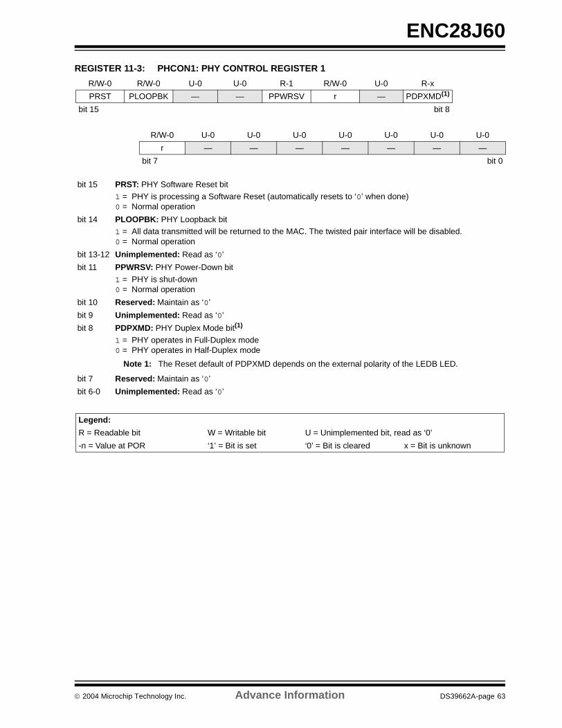
ENC28J60
REGISTER 11-3: PHCON1: PHY CONTROL REGISTER 1
bit 15 PRST: PHY Software Reset bit
1 = PHY is processing a Software Reset (automatically resets to ‘0’ when done)0 = Normal operation
bit 14 PLOOPBK: PHY Loopback bit1 = All data transmitted will be returned to the MAC. The twisted pair interface will be disabled.0 = Normal operation
bit 13-12 Unimplemented: Read as ‘0’
bit 11 PPWRSV: PHY Power-Down bit
1 = PHY is shut-down0 = Normal operation
bit 10 Reserved: Maintain as ‘0’
bit 9 Unimplemented: Read as ‘0’
bit 8 PDPXMD: PHY Duplex Mode bit(1)
1 = PHY operates in Full-Duplex mode0 = PHY operates in Half-Duplex mode
Note 1: The Reset default of PDPXMD depends on the external polarity of the LEDB LED.
bit 7 Reserved: Maintain as ‘0’
bit 6-0 Unimplemented: Read as ‘0’
R/W-0 R/W-0 U-0 U-0 R-1 R/W-0 U-0 R-x
PRST PLOOPBK — — PPWRSV r — PDPXMD(1)
bit 15 bit 8
R/W-0 U-0 U-0 U-0 U-0 U-0 U-0 U-0
r — — — — — — —
bit 7 bit 0
Legend:
R = Readable bit W = Writable bit U = Unimplemented bit, read as ‘0’
-n = Value at POR ‘1’ = Bit is set ‘0’ = Bit is cleared x = Bit is unknown
2004 Microchip Technology Inc. Advance Information DS39662A-page 63

ENC28J60
NOTES:
DS39662A-page 64 Advance Information 2004 Microchip Technology Inc.

ENC28J60
12.0 INTERRUPTS
The ENC28J60 has multiple interrupt sources and twoseparate interrupt output pins to signal the occurrenceof events to the host controller. The interrupt pins aredesigned for use by a host controller which is capableof detecting falling edges.
Interrupts are divided into two sources: control events(INT) and Wake-up on LAN (WOL) events. The EIE andEWOLIE registers contain the individual interruptenable bits for each interrupt source, while the EIR andEWOLIR registers contain the corresponding interruptflag bits. When an interrupt occurs, the interrupt flag isset. If the interrupt is enabled in the EIE or EWOLIEregisters and the corresponding INTIE or WOLIE globalinterrupt enable bit is set, the appropriate INT or WOLinterrupt pin will be driven low by the ENC28J60 (seeFigure 12-1).
When an enabled interrupt occurs, the interrupt pin willremain low until all flags which are causing the interruptare cleared or masked off (enable bit is cleared) by thehost controller. If more than one interrupt source isenabled, the host controller must poll each flag in theEIR or EWOLIR register to determine the source(s) ofthe interrupt. It is recommended that the Bit Field Clear(BFC) SPI command be used to reset the flag bits in theEIR and EWOLIR registers rather than the normalWrite Control Register (WCR) command. This isnecessary to prevent unintentionally altering a flag thatchanges during the write command. The BFC andWCR commands are discussed in detail in Section 4.0“Serial Peripheral Interface (SPI)”.
After an interrupt occurs, the host controller shouldclear the global enable bit for the interrupt pin beforeservicing the interrupt. Clearing the enable bit willcause the interrupt pin to return to the non-assertedstate (high). Doing so will prevent the host controllerfrom missing a falling edge should another interruptoccur while the immediate interrupt is being serviced.After the interrupt has been serviced, the global enablebit may be restored. If an interrupt event occurred whilethe previous interrupt was being processed, the act ofresetting the global enable bit will cause a new fallingedge on the interrupt pin to occur.
FIGURE 12-1: ENC28J60 INTERRUPT LOGIC
Note: Except for the LINKIF interrupt flag,interrupt flag bits are set when an interruptcondition occurs regardless of the state ofits corresponding enable bit or the associ-ated global enable bit. User softwareshould ensure the appropriate interrupt flagbits are clear prior to enabling an interrupt.This feature allows for software polling.
PKTIF
PKTIE
DMAIF
DMAIE
WOLIE
LINKIE
TXIF
TXIE
INT
INTIETXERIF
TXERIE
WOL
UCWOLIF
UCWOLIE
PMWOLIF
PMWOLIE
MPWOLIF
MPWOLIE
HTWOLIF
HTWOLIE
MCWOLIF
MCWOLIE
BCWOLIF
BCWOLIE
RXERIF
RXERIE
AWOLIF
AWOLIE
LINKIFPGIF
PGEIE
PLNKIF
PLNKIE INT
WOLIF
2004 Microchip Technology Inc. Advance Information DS39662A-page 65

ENC28J60
12.1 INT Interrupt Enable (INTIE)
The INT Interrupt Enable bit (INTIE) is a global enablebit which allows the following interrupts to drive the INTpin:
• Receive Error Interrupt (RXERIF)• Transmit Error Interrupt (TXERIF)• Transmit Interrupt (TXIF)
• Link Change Interrupt (LINKIF)• DMA Interrupt (DMAIF)• Receive Packet Pending Interrupt (PKTIF)
When any of the above interrupts are enabled andgenerated, the virtual bit, INT in the ESTAT register(Register 12-1), will be set to ‘1’. If EIE.INTIE is ‘1’, theINT pin will be driven low.
12.1.1 INT INTERRUPT REGISTERS
The registers associated with the INT interrupts areshown in Register 12-2, Register 12-3, Register 12-4and Register 12-5.
REGISTER 12-1: ESTAT: ETHERNET STATUS REGISTER R-0 R/C-0 R-0 R/C-0 U-0 R-0 R/C-0 R/W-0
INT r r LATECOL — RXBUSY TXABRT CLKRDY
bit 7 bit 0
bit 7 INT: INT Interrupt Flag bit1 = INT interrupt is pending0 = No INT interrupt is pending
bit 6-5 Reserved: Maintain as ‘0’
bit 4 LATECOL: Late Collision Error bit1 = A collision occurred after 64 bytes have been transmitted0 = No collisions after 64 bytes have occurred
bit 3 Unimplemented: Read as ‘0’
bit 2 RXBUSY: Receive Busy bit
1 = Receive logic is receiving a data packet0 = Receive logic is Idle
bit 1 TXABRT: Transmit Abort Error bit1 = The transmit request was aborted0 = No transmit abort error
bit 0 CLKRDY: Clock Ready bit1 = OST has expired; PHY is ready0 = OST is still counting; PHY is not ready
Legend:
R = Readable bit C = Clearable bit U = Unimplemented bit, read as ‘0’
-n = Value at POR ‘1’ = Bit is set ‘0’ = Bit is cleared r = Reserved bit
DS39662A-page 66 Advance Information 2004 Microchip Technology Inc.

ENC28J60
REGISTER 12-2: EIE: ETHERNET INTERRUPT ENABLE REGISTER R/W-0 R/W-0 R/W-0 R/W-0 R/W-0 R/W-0 R/W-0 R/W-0
INTIE PKTIE DMAIE LINKIE TXIE WOLIE TXERIE RXERIE
bit 7 bit 0
bit 7 INTIE: Global INT Interrupt Enable bit1 = Allow interrupt events to drive the INT pin0 = Disable all INT pin activity (pin is continuously driven high)
bit 6 PKTIE: Receive Packet Pending Interrupt Enable bit
1 = Enable receive packet pending interrupt0 = Disable receive packet pending interrupt
bit 5 DMAIE: DMA Interrupt Enable bit1 = Enable DMA interrupt0 = Disable DMA interrupt
bit 4 LINKIE: Link Status Change Interrupt Enable bit1 = Enable link change interrupt from the PHY0 = Disable link change interrupt
bit 3 TXIE: Transmit Enable bit
1 = Enable transmit interrupt0 = Disable transmit interrupt
bit 2 WOLIE: Global WOL Interrupt Enable bit1 = Allow WOL interrupt events to drive the WOL pin0 = Disable all WOL pin activity (pin is continuously driven high)
bit 1 TXERIE: Transmit Error Interrupt Enable bit1 = Enable transmit error interrupt0 = Disable transmit error interrupt
bit 0 RXERIE: Receive Error Interrupt Enable bit
1 = Enable receive error interrupt0 = Disable receive error interrupt
Legend:
R = Readable bit W = Writable bit U = Unimplemented bit, read as ‘0’
-n = Value at POR ‘1’ = Bit is set ‘0’ = Bit is cleared x = Bit is unknown
2004 Microchip Technology Inc. Advance Information DS39662A-page 67

ENC28J60
REGISTER 12-3: EIR: ETHERNET INTERRUPT REQUEST (FLAG) REGISTER U-0 R-0 R/C-0 R-0 R/C-0 R-0 R/C-0 R/C-0
— PKTIF DMAIF LINKIF TXIF WOLIF TXERIF RXERIF
bit 7 bit 0
bit 7 Unimplemented: Read as ‘0’
bit 6 PKTIF: Receive Packet Pending Interrupt Flag bit
1 = Receive buffer contains one or more unprocessed packets; cleared when PKTDEC is set0 = Receive buffer is empty
bit 5 DMAIF: DMA Interrupt Flag bit1 = DMA copy or checksum calculation has completed0 = No DMA interrupt is pending
bit 4 LINKIF: Link Change Interrupt Flag bit1 = PHY reports that the link status has changed; read PHIR register to clear0 = Link status has not changed
bit 3 TXIF: Transmit Interrupt Flag bit
1 = Transmit request has ended0 = No transmit interrupt is pending
bit 2 WOLIF: WOL Interrupt Flag bit1 = Wake-up on LAN interrupt is pending0 = No Wake-up on LAN interrupt is pending
bit 1 TXERIF: Transmit Error Interrupt Flag bit1 = A transmit error has occurred0 = No transmit error has occurred
bit 0 RXERIF: Receive Error Interrupt Flag bit
1 = A packet was aborted because there is insufficient buffer space or the packet count is 2550 = No receive error interrupt is pending
Legend:
R = Readable bit C = Clearable bit U = Unimplemented bit, read as ‘0’
-n = Value at POR ‘1’ = Bit is set ‘0’ = Bit is cleared x = Bit is unknown
DS39662A-page 68 Advance Information 2004 Microchip Technology Inc.
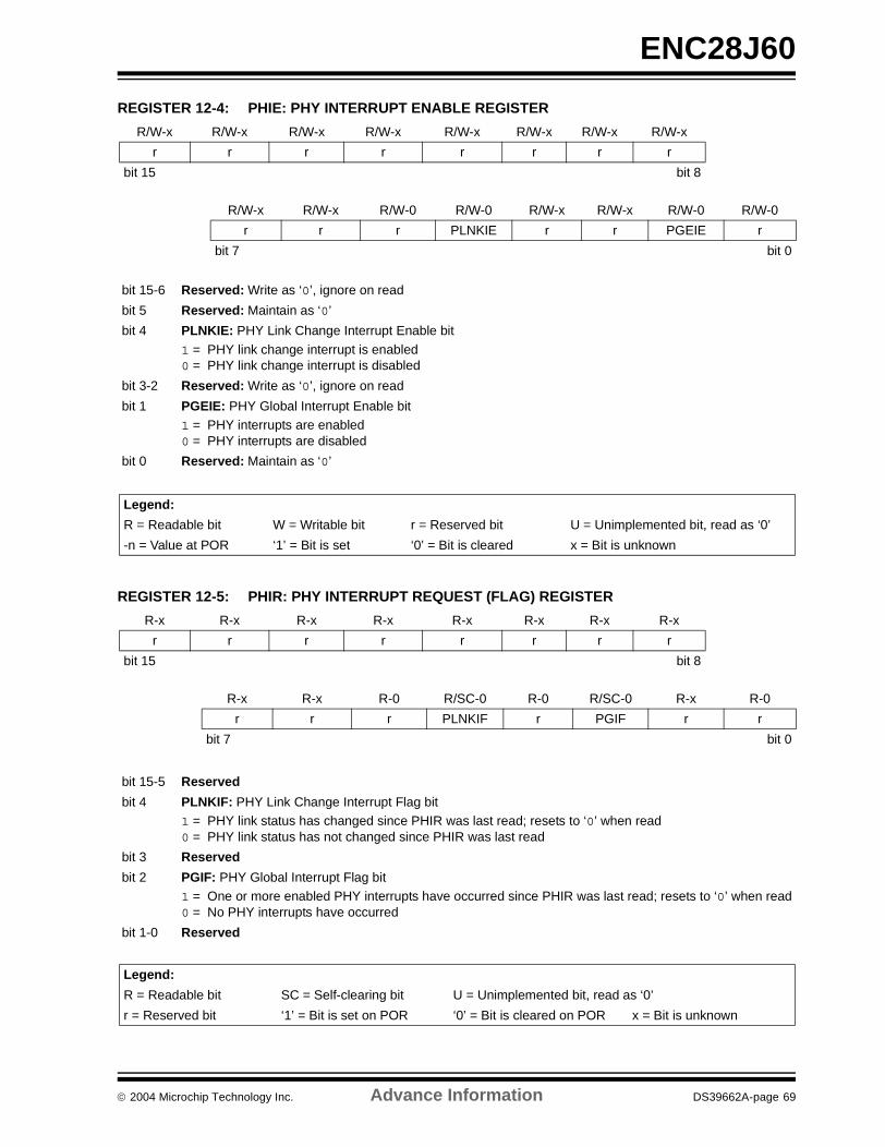
ENC28J60
REGISTER 12-4: PHIE: PHY INTERRUPT ENABLE REGISTER
bit 15-6 Reserved: Write as ‘0’, ignore on read
bit 5 Reserved: Maintain as ‘0’
bit 4 PLNKIE: PHY Link Change Interrupt Enable bit
1 = PHY link change interrupt is enabled0 = PHY link change interrupt is disabled
bit 3-2 Reserved: Write as ‘0’, ignore on read
bit 1 PGEIE: PHY Global Interrupt Enable bit1 = PHY interrupts are enabled0 = PHY interrupts are disabled
bit 0 Reserved: Maintain as ‘0’
REGISTER 12-5: PHIR: PHY INTERRUPT REQUEST (FLAG) REGISTER
bit 15-5 Reserved
bit 4 PLNKIF: PHY Link Change Interrupt Flag bit1 = PHY link status has changed since PHIR was last read; resets to ‘0’ when read0 = PHY link status has not changed since PHIR was last read
bit 3 Reserved
bit 2 PGIF: PHY Global Interrupt Flag bit1 = One or more enabled PHY interrupts have occurred since PHIR was last read; resets to ‘0’ when read0 = No PHY interrupts have occurred
bit 1-0 Reserved
R/W-x R/W-x R/W-x R/W-x R/W-x R/W-x R/W-x R/W-x
r r r r r r r r
bit 15 bit 8
R/W-x R/W-x R/W-0 R/W-0 R/W-x R/W-x R/W-0 R/W-0
r r r PLNKIE r r PGEIE r
bit 7 bit 0
Legend:
R = Readable bit W = Writable bit r = Reserved bit U = Unimplemented bit, read as ‘0’
-n = Value at POR ‘1’ = Bit is set ‘0’ = Bit is cleared x = Bit is unknown
R-x R-x R-x R-x R-x R-x R-x R-x
r r r r r r r r
bit 15 bit 8
R-x R-x R-0 R/SC-0 R-0 R/SC-0 R-x R-0
r r r PLNKIF r PGIF r r
bit 7 bit 0
Legend:
R = Readable bit SC = Self-clearing bit U = Unimplemented bit, read as ‘0’
r = Reserved bit ‘1’ = Bit is set on POR ‘0’ = Bit is cleared on POR x = Bit is unknown
2004 Microchip Technology Inc. Advance Information DS39662A-page 69

ENC28J60
12.1.2 RECEIVE ERROR INTERRUPT FLAG (RXERIF)
The Receive Error Interrupt Flag (RXERIF) is used toindicate a receive buffer overflow condition. Alternately,this interrupt may indicate that too many packets are inthe receive buffer and more cannot be stored withoutoverflowing the EPKTCNT register.
When a packet is being received and the receive bufferruns completely out of space, or EPKTCNT is 255 andcannot be incremented, the packet being received willbe aborted (permanently lost) and the EIR.RXERIF bitwill be set to ‘1’. Once set, RXERIF can only be clearedby the host controller or by a Reset condition. If thereceive error interrupt and INT interrupt are enabled(EIE.RXERIE = 1 and EIE.INTIE = 1), an interrupt isgenerated by driving the INT pin low. If the receive errorinterrupt is not enabled (EIE.RXERIE = 0 or EIE.INTIE= 0), the host controller may poll the ENC28J60 for theRXERIF and take appropriate action.
Normally, upon the receive error condition, the hostcontroller would process any packets pending from thereceive buffer and then make additional room for futurepackets by advancing the ERXRDPT registers (lowbyte first) and decrementing the EPKTCNT register.See Section 7.2.4 “Freeing Receive Buffer Space”for more information on processing packets. Onceprocessed, the host controller should use the BFCcommand to clear the EIR.RXERIF bit.
12.1.3 TRANSMIT ERROR INTERRUPT FLAG (TXERIF)
The Transmit Error Interrupt Flag (TXERIF) is used toindicate that a transmit abort has occurred. An abortcan occur because of any of the following:
1. Excessive collisions occurred as defined by theRetransmission Maximum (RETMAX) bits in theMACLCON1 register.
2. A late collision occurred as defined by theCollision Window (COLWIN) bits in theMACLCON2 register.
3. A collision after transmitting 64 bytes occurred(ESTAT.LATECOL set).
4. The transmission was unable to gain anopportunity to transmit the packet because themedium was constantly occupied for too long.The deferral limit (2.4287 ms) was reached andthe MACON4.DEFER bit was clear.
5. An attempt to transmit a packet larger than themaximum frame length defined by the MAMXFLregisters was made without setting theMACON3.HFRMEN bit or per packetPOVERRIDE and PHUGEEN bits.
Upon any of these conditions, the EIR.TXERIF flag is setto ‘1’. Once set, it can only be cleared by the hostcontroller or by a Reset condition. If the transmit errorinterrupt is enabled (EIE.TXERIE = 1 and EIE.INTIE = 1),an interrupt is generated by driving the INT pin low forone OSC1 period. If the transmit error interrupt is notenabled (EIE.TXERIE = 0 or EIE.INTIE = 0), the hostcontroller may poll the ENC28J60 for the TXERIF andtake appropriate action. Once the interrupt is processed,the host controller should use the BFC command to clearthe EIR.TXERIF bit.
After a transmit abort, the TXRTS bit will be cleared, theESTAT.TXABRT bit will be set and the transmit statusvector will be written at ETXND + 1. The MAC will notautomatically attempt to retransmit the packet. Thehost controller may wish to read the transmit statusvector and LATECOL bit to determine the cause of theabort. After determining the problem and solution, thehost controller should clear the LATECOL (if set) andTXABRT bits so that future aborts can be detectedaccurately.
In Full-Duplex mode, condition 5 is the only one thatshould cause this interrupt. Collisions and other prob-lems related to sharing the network are not possible onfull-duplex networks. The conditions which cause thetransmit error interrupt meet the requirements of thetransmit interrupt. As a result, when this interruptoccurs, TXIF will also be simultaneously set.
12.1.4 TRANSMIT INTERRUPT FLAG (TXIF)
The Transmit Interrupt Flag (TXIF) is used to indicatethat the requested packet transmission has ended(ECON1.TXRTS has transitioned from ‘1’ to ‘0’). Upontransmission completion, abort or transmission cancella-tion by the host controller, the EIR.TXIF flag will be set to‘1’. If the host controller did not clear the TXRTS bit andthe ESTAT.TXABRT bit is not set, then the packet wassuccessfully transmitted. Once TXIF is set, it can only becleared by the host controller or by a Reset condition. Ifthe transmit interrupt is enabled (EIE.TXIE = 1 andEIE.INTIE = 1), an interrupt is generated by driving theINT pin low. If the transmit interrupt is not enabled(EIE.TXIE = 0 or EIE.INTIE = 0), the host controller maypoll the ENC28J60 for the TXIF bit and take appropriateaction. Once processed, the host controller should usethe BFC command to clear the EIR.TXIF bit.
DS39662A-page 70 Advance Information 2004 Microchip Technology Inc.

ENC28J60
12.1.5 LINK CHANGE INTERRUPT FLAG (LINKIF)
The LINKIF indicates that the link status has changed.The actual current link status can be obtained from thePHSTAT1.LLSTAT or PHSTAT2.LSTAT (see Register 3-6and Register 3-7). Unlike other interrupt sources, the linkstatus change interrupt is created in the integrated PHYmodule; additional steps must be taken to enable it.
By Reset default, LINKIF is never set for any reason. Toreceive it, the host controller must set thePHIE.PLNKIE and PGEIE bits. After setting the twoPHY interrupt enable bits, the LINKIF bit will thenshadow the contents of the PHIR.PGIF bit. The PHYonly supports one interrupt, so the PGIF bit will alwaysbe the same as the PHIR.PLNKIF bit (when both PHYenable bits are set).
Once LINKIF is set, it can only be cleared by the hostcontroller or by a Reset. If the link change interruptis enabled (EIE.LINKIE = 1, EIE.INTIE = 1,PHIE.PLNKIE = 1 and PHIE.PGEIE = 1), an interruptwill be generated by driving the INT pin low. If the linkchange interrupt is not enabled (EIE.LINKIE = 0,EIE.INTIE = 0, PHIE.PLNKIE = 0 or PHIE.PGEIE = 0),the host controller may poll the ENC28J60 for thePHIR.PLNKIF bit and take appropriate action.
The LINKIF bit is read-only. Because reading from PHYregisters requires non-negligible time, the host controllermay instead set PHIE.PLNKIE and PHIE.PGEIE andthen poll the EIR.LINKIF bit. Performing an MII read onthe PHIR register will clear the LINKIF, PGIF andPLNKIF bits automatically and allow for future link statuschange interrupts. See Section 3.3 “PHY Registers”for information on accessing the PHY registers.
12.1.6 DMA INTERRUPT FLAG (DMAIF)
The DMA interrupt indicates that the DMA module hascompleted its memory copy or checksum calculation(ECON1.DMAST has transitioned from ‘1’ to ‘0’). Addi-tionally, this interrupt will be caused if the host controllercancels a DMA operation by manually clearing theDMAST bit. Once set, DMAIF can only be cleared by thehost controller or by a Reset condition. If the DMAinterrupt is enabled (EIE.DMAIE = 1 and EIE.INTIE = 1),an interrupt is generated by driving the INT pin low. If theDMA interrupt is not enabled (EIE.DMAIE = 0 orEIE.INTIE = 0), the host controller may poll theENC28J60 for the DMAIF and take appropriate action.Once processed, the host controller should use the BFCcommand to clear the EIR.DMAIF bit.
12.1.7 RECEIVE PACKET PENDING INTERRUPT FLAG (PKTIF)
The Receive Packet Pending Interrupt Flag (PKTIF) isused to indicate the presence of one or more data pack-ets in the receive buffer and to provide a notificationmeans for the arrival of new packets. When the receivebuffer has at least one packet in it, EIR.PKTIF will be set.In other words, this interrupt flag will be set anytime theEthernet Packet Count register (EPKTCNT) is non-zero.If the receive packet pending interrupt is enabled(EIE.PKTIE = 1 and EIE.INTIE = 1), an interrupt will begenerated by driving the INT pin low whenever a newpacket is successfully received and written into thereceive buffer. If the receive packet pending interrupt isnot enabled (EIE.PKTIE = 0 or EIE.INTIE = 0), the hostcontroller will not be notified when new packets arrive.However, it may poll the PKTIF bit and take appropriateaction.
The PKTIF bit can only be cleared by the host controlleror by a Reset condition. In order to clear PKTIF, theEPKTCNT register must be decremented to ‘0’. SeeSection 7.2 “Receiving Packets” for more informa-tion about clearing the EPKTCNT register. If the lastdata packet in the receive buffer is processed,EPKTCNT will become zero and the PKTIF bit willautomatically be cleared.
12.2 Wake-up on LAN Interrupt (WOLIE/WOLIF)
The WOL interrupt is designed to cause a wake-upevent for the host controller. The WOL interrupt is amultisource interrupt and controls the WOL interruptpin. WOL interrupts are not affected by the EIE.INTIEconfiguration.
There are a total of seven different conditions that cancause this interrupt. The EWOLIE bits allow the individ-ual conditions to be enabled. If multiple bits are set, anyof the enabled conditions will be able to generate theWOL interrupt. However, the WOL filter logic is appliedafter the receive filter logic. As a result, any packetwhich is rejected as a result of the receive filter config-uration (see Section 8.0 “Receive Filters”) will not beable to cause a WOL interrupt.
2004 Microchip Technology Inc. Advance Information DS39662A-page 71

ENC28J60
When any of the seven WOL conditions are detected,the associated interrupt flag in the EWOLIR register willbe set. If the associated interrupt enable is set inEWOLIE, then the EIR.WOLIF bit will also become set.If the global WOL interrupt enable bit is set(EIR.WOLIF), then an interrupt will be generated bydriving the WOL pin low. If the WOL interrupt is notenabled (EIE.WOLIE = 0 or the associated bit inEWOLIE = 0), the host controller may poll the EWOLIRregister and take appropriate action when the desiredflag becomes set. Normally, upon receiving the WOLIFinterrupt, the host controller would come out of Sleepand check the EWOLIR register for the actual source(s)of the interrupt. Depending on the application require-ments, the host controller may either disable furtherWOLIF interrupts or keep it enabled and go back toSleep. Once the interrupt is processed, the hostcontroller should use the BFC command to clear theEIR.WOLIF bit and associated EWOLIR bits.
12.2.1 WOL INTERRUPT REGISTERS
The registers associated with the WOL interrupts areshown in Register 12-6 and Register 12-7. The inter-rupt flag bits are set when an interrupt condition occursregardless of the state of its corresponding enable bit.This feature allows for software polling.
REGISTER 12-6: EWOLIE: ETHERNET WAKE-UP ON LAN INTERRUPT ENABLE REGISTER
Note: When using the WOL interrupt, careshould be taken to prevent the receivebuffer from filling up without waking thehost controller. If the receive bufferbecomes full, without meeting any of theWOL criteria, all additional incoming pack-ets will be aborted. Aborted packets arenot able to cause the WOL interrupt, evenif they meet the configured criteria. As aresult, the WOL interrupt would never begenerated.
R/W-0 R/W-0 U-0 R/W-0 R/W-0 R/W-0 R/W-0 R/W-0
UCWOLIE AWOLIE — PMWOLIE MPWOLIE HTWOLIE MCWOLIE BCWOLIE
bit 7 bit 0
bit 7 UCWOLIE: Unicast Wake-up on LAN Interrupt Enable bit1 = Enable Unicast Wake-up on LAN interrupt0 = Disable Unicast Wake-up on LAN interrupt
bit 6 AWOLIE: Any Packet Wake-up on LAN Interrupt Enable bit1 = Enable Any Packet Wake-up on LAN interrupt0 = Disable Any Packet Wake-up on LAN interrupt
bit 5 Unimplemented: Read as ‘0’
bit 4 PMWOLIE: Pattern Match Wake-up on LAN Interrupt Enable bit1 = Enable Pattern Match Wake-up on LAN interrupt0 = Disable Pattern Match Wake-up on LAN interrupt
bit 3 MPWOLIE: Magic Packet Wake-up on LAN Interrupt Enable bit1 = Enable Magic Packet Wake-up on LAN interrupt0 = Disable Magic Packet Wake-up on LAN interrupt
bit 2 HTWOLIE: Hash Table Wake-up on LAN Interrupt Enable bit1 = Enable Hash Table Wake-up on LAN interrupt0 = Disable Hash Table Wake-up on LAN interrupt
bit 1 MCWOLIE: Multicast Packet Wake-up on LAN Interrupt Enable bit1 = Enable Mulitcast Packet Wake-up on LAN interrupt0 = Disable Multicast Packet Wake-up on LAN interrupt
bit 0 BCWOLIE: Broadcast Packet Wake-up on LAN Interrupt Enable bit1 = Enable Broadcast Packet Wake-up on LAN interrupt0 = Disable Broadcast Packet Wake-up on LAN interrupt
Legend:
R = Readable bit W = Writable bit U = Unimplemented bit, read as ‘0’
-n = Value at POR ‘1’ = Bit is set ‘0’ = Bit is cleared x = Bit is unknown
DS39662A-page 72 Advance Information 2004 Microchip Technology Inc.

ENC28J60
REGISTER 12-7: EWOLIR: ETHERNET WAKE-UP ON LAN INTERRUPT REQUEST (FLAG) REGISTER
R/C-0 R/C-0 U-0 R/C-0 R/C-0 R/C-0 R/C-0 R/C-0
UCWOLIF AWOLIF — PMWOLIF MPWOLIF HTWOLIF MCWOLIF BCWOLIF
bit 7 bit 0
bit 7 UCWOLIF: Unicast Wake-up on LAN Interrupt Flag bit1 = A packet was received with a destination address matching the local MAC address0 = No unicast packets matching the local MAC address have been received
bit 6 AWOLIF: Any Packet Wake-up on LAN Interrupt Flag bit1 = A packet was received0 = No packets have been received
bit 5 Unimplemented: Read as ‘0’
bit 4 PMWOLIF: Pattern Match Wake-up on LAN Interrupt Flag bit1 = A packet was received which passed the pattern match filter critieria0 = No packets matching the pattern match criteria have been received
bit 3 MPWOLIF: Magic Packet Wake-up on LAN Interrupt Flag bit1 = A Magic Packet for the local MAC address was received0 = No Magic Packets for the local MAC address have been received
bit 2 HTWOLIF: Hash Table Wake-up on LAN Interrupt Flag bit1 = A packet was received which passed the hash table filter criteria0 = No packets matching the hash table filter criteria have been received
bit 1 MCWOLIF: Multicast Packet Wake-up on LAN Interrupt Flag bit1 = A packet was received with a multicast destination address0 = No packets with a multicast destination address have been received
bit 0 BCWOLIF: Broadcast Packet Wake-up on LAN Interrupt Flag bit1 = A packet was received with a destination address of FF-FF-FF-FF-FF-FF0 = No packets with a broadcast destination address have been received
Legend:
R = Readable bit C = Clearable bit U = Unimplemented bit, read as ‘0’
-n = Value at POR ‘1’ = Bit is set ‘0’ = Bit is cleared x = Bit is unknown
2004 Microchip Technology Inc. Advance Information DS39662A-page 73

ENC28J60
NOTES:
DS39662A-page 74 Advance Information 2004 Microchip Technology Inc.

ENC28J60
13.0 DIRECT MEMORY ACCESS CONTROLLER
The ENC28J60 incorporates a dual purpose DMAcontroller which can be used to copy data betweenlocations within the 8-Kbyte memory buffer. It can alsobe used to calculate a 16-bit checksum which iscompatible with various industry standard protocols,including TCP and IP.
When a DMA operation begins, the EDMAST registerpair is copied into an internal source pointer. The DMAwill execute on one byte at a time and then incrementthe internal source pointer. However, if a byte isprocessed and the internal source pointer is equal tothe receive buffer end pointer, ERXND, the sourcepointer will not be incremented. Instead, the internalsource pointer will be loaded with the receive bufferstart pointer, ERXST. In this way, the DMA will followthe circular FIFO structure of the receive buffer andreceived packets can be processed using one opera-tion. The DMA operation will end when the internalsource pointer matches the EDMAND pointer.
While any DMA operation is in progress, the DMApointers and the ECON1.CSUMEN bit should not bemodified. The DMA operation can be canceled at anytime by clearing the ECON1.DMAST bit. No registerswill change; however, some memory bytes may alreadyhave been copied if a DMA copy was in progress.
13.1 Copying Memory
To copy memory within the buffer:
1. Appropriately program the EDMAST, EDMANDand EDMADST register pairs. The EDMASTregisters should point to the first byte to copyfrom, the EDMAND registers should point to thelast byte to copy and the EDMADST registersshould point to the first byte in the destinationrange. The destination range will always belinear, never wrapping at any values except from8191 to 0 (the 8-Kbyte memory boundary).Extreme care should be taken whenprogramming the start and end pointers toprevent a never ending DMA operation whichwould overwrite the entire 8-Kbyte buffer.
2. If an interrupt at the end of the copy process isdesired, set EIE.DMAIE and EIE.INTIE andclear EIR.DMAIF.
3. Verify that ECON1.CSUMEN is clear.
4. Start the DMA copy by setting ECON1.DMAST.
If a transmit operation is in progress (TXRTS set) whilethe DMAST bit is set, the ENC28J60 will wait until thetransmit operation is complete before attempting to dothe DMA copy. This possible delay is required becausethe DMA and transmission engine share the samememory access port.
When the copy is complete, the DMA hardware willclear the DMAST bit, set the DMAIF bit and generatean interrupt (if enabled). The pointers and theEDMACS registers will not be modified.
After the DMA module has been initialized and hasbegun its copy, two main clock cycles will be requiredfor each byte copied. As a result, if a maximum size1518-byte packet was copied, the DMA module wouldrequire slightly more than 121.44 µs to complete. Thetime required to copy a minimum size packet of64 bytes would be dominated by the time required toconfigure the DMA.
Note 1: If the EDMAND pointer cannot bereached because of the receive bufferwrapping behavior, the DMA operationwill never end.
2: By design, the DMA module cannotbe used to copy only one byte(EDMAST = EDMAND). An attempt todo so will overwrite all memory in thebuffer and may never end.
2004 Microchip Technology Inc. Advance Information DS39662A-page 75

ENC28J60
13.2 Checksum Calculations
The checksum calculation logic treats the source data asa series of 16-bit big-endian integers. If the source rangecontains an odd number of bytes, a padding byte of 00his effectively added to the end of the series for purposesof calculating the checksum. The calculated checksumis the 16-bit one’s complement of the one’s complementsum of all 16-bit integers. For example, if the bytesincluded in the checksum were 89h, ABh, CDh, thechecksum would begin by computing 89ABh + CD00h.A carry out of the 16th bit would occur in the example, soin 16-bit one’s complement arithmetic, it would be addedback to the first bit. The resulting value of 56ACh wouldfinally be complemented to achieve a checksum ofA953h.
To calculate a checksum:
1. Program the EDMAST and EDMAND registerpairs to point to the first and last bytes of bufferdata to be included in the checksum. Care shouldbe taken when programming these pointers toprevent a never ending checksum calculationdue to receive buffer wrapping.
2. To generate an optional interrupt when thechecksum calculation is done, clear EIR.DMAIF,set EIE.DMAIE and set EIE.INTIE.
3. Start the calculation by setting ECON1.CSUMENand ECON1.DMAST.
When the checksum is finished being calculated, thehardware will clear the DMAST bit, set the DMAIF bitand an interrupt will be generated if enabled. The DMA
pointers will not be modified and no memory will bewritten to. The EDMACSH and EDMACSL registers willcontain the calculated checksum. The host controllermay write this value into a packet, compare this valuewith a received checksum, or use it for other purposes.
Various protocols, such as TCP and IP, have a checksumfield inside a range of data which the checksum covers.If such a packet is received and the host controller needsto validate the checksum, it can do the following:
1. Read the checksum from the packet and save itto a temporary location
2. Write zeros to the checksum field.3. Calculate a new checksum using the DMA
controller.4. Compare the results with the saved checksum
from step 1.
Writing to the receive buffer is permitted when the writeaddress is protected by means of the ERXRDPTpointers. See Section 7.2 “Receiving Packets” foradditional information.
The IP checksum has unique mathematical propertieswhich may be used in some cases to reduce theprocessing requirements further. Writing to the receivebuffer may be unnecessary in some applications.
When operating the DMA in Checksum mode, it willtake one main clock cycle for every byte included in thechecksum. As a result, if a checksum over 1446 byteswere performed, the DMA module would requireslightly more than 57.84 µs to complete the operation.
TABLE 13-1: SUMMARY OF REGISTERS ASSOCIATED WITH THE DMA CONTROLLER
RegisterName
Bit 7 Bit 6 Bit 5 Bit 4 Bit 3 Bit 2 Bit 1 Bit 0Reset Values
on page
EIE INTIE PKTIE DMAIE LINKIE TXIE WOLIE TXERIE RXERIE 13
EIR — PKTIF DMAIF LINKIF TXIF WOLIF TXERIF RXERIF 13
ECON1 TXRST RXRST DMAST CSUMEN TXRTS RXEN BSEL1 BSEL0 13
ERXNDL RX End Low Byte (ERXND<7:0>) 13
ERXNDH — — — RX End High Byte (ERXND<12:8>) 13
EDMASTL DMA Start Low Byte (EDMAST<7:0>) 13EDMASTH — — — DMA Start High Byte (EDMAST<12:8>) 13EDMANDL DMA End Low Byte (EDMAND<7:0>) 13EDMANDH — — — DMA End High Byte (EDMAND<12:8>) 13EDMADSTL DMA Destination Low Byte (EDMADST<7:0>) 13EDMADSTH — — — DMA Destination High Byte (EDMADST<12:8>) 13EDMACSL DMA Checksum Low Byte (EDMACS<7:0>) 13
EDMACSH DMA Checksum High Byte (EDMACS<15:8>) 13
Legend: — = unimplemented, read as ‘0’. Shaded cells are not used with the DMA controller.
DS39662A-page 76 Advance Information 2004 Microchip Technology Inc.

ENC28J60
14.0 POWER-DOWN
The ENC28J60 may be commanded to power-downvia the SPI interface. When powered down, it will nolonger be able to transmit and receive any packets.
To maximize power savings:
1. Turn off packet reception by clearingECON1.RXEN.
2. Wait for any in-progress packets to finish beingreceived by polling ESTAT.RXBUSY. This bitshould be clear before proceeding.
3. Wait for any current transmissions to end byconfirming ECON1.TXRTS is clear.
4. Set ECON2.VRPS (if not already set).5. Enter Sleep by setting ECON2.PWRSV. All
MAC, MII and PHY registers becomeinaccessible as a result. Setting PWRSV alsoclears ESTAT.CLKRDY automatically.
In Sleep mode, all registers and buffer memory willmaintain their states. The ETH registers and buffermemory will still be accessible by the host controller.Additionally, the clock driver will continue to operate.The CLKOUT function will be unaffected (seeSection 2.3 “CLKOUT Pin”).
When normal operation is desired, the host controllermust perform a slightly modified procedure:
1. Wake-up by clearing ECON2.PWRSV.2. Wait at least 300 µs for the PHY to stabilize. To
accomplish the delay, the host controller maypoll ESTAT.CLKRDY and wait for it to becomeset.
3. Restore receive capability by settingECON1.RXEN.
After leaving Sleep mode, there is a delay of manymilliseconds before a new link is established (assumingan appropriate link partner is present). The hostcontroller may wish to wait until the link is establishedbefore attempting to transmit any packets. The linkstatus can be determined by polling thePHSTAT2.LSTAT bit. Alternatively, the link changeinterrupt may be used if it is enabled. SeeSection 12.1.5 “Link Change Interrupt Flag(LINKIF)” for additional details.
TABLE 14-1: SUMMARY OF REGISTERS USED WITH POWER-DOWN
Name Bit 7 Bit 6 Bit 5 Bit 4 Bit 3 Bit 2 Bit 1 Bit 0Reset Values
on page
ESTAT INT r r LATECOL — RXBUSY TXABRT CLKRDY 13
ECON2 AUTOINC PKTDEC PWRSV — VRPS — — — 13
ECON1 TXRST RXRST DMAST CSUMEN TXRTS RXEN BSEL1 BSEL0 13
Legend: — = unimplemented, read as ‘0’, r = reserved bit. Shaded cells are not used for power-down.
2004 Microchip Technology Inc. Advance Information DS39662A-page 77

ENC28J60
NOTES:
DS39662A-page 78 Advance Information 2004 Microchip Technology Inc.

ENC28J60
15.0 BUILT-IN SELF-TEST CONTROLLER
The ENC28J60 features a Built-in Self-Test (BIST)module which is designed to confirm proper operationof each bit in the 8-Kbyte memory buffer. Although it isprimarily useful for testing during manufacturing, itremains present and available for diagnostic purposesby the user. The controller writes to all locations in thebuffer memory and requires several pieces of hardwareshared by normal Ethernet operations. Thus, the BISTshould only be used on Reset or after necessaryhardware is freed. When the BIST is used, the ECON1register’s DMAST, RXEN and TXRTS bits should all beclear.
The BIST controller is operated through four registers:
• EBSTCON register (control and status register)• EBSTSD register (fill seed/initial shift value)
• EBSTCSH and EBSTCSL registers (high and low bytes of generated checksum)
The EBSTCON register (Register 15-1) controls themodule’s overall operation, selecting the testing modesand starting the self-test process. The bit pattern formemory tests is provided by the EBSTSD seed regis-ter; its content is either used directly, or as the seed fora pseudo-random number generator, depending on theTest mode.
REGISTER 15-1: EBSTCON: SELF-TEST CONTROL REGISTER R/W-0 R/W-0 R/W-0 R/W-0 R/W-0 R/W-0 R/W-0 R/W-0
PSV2 PSV1 PSV0 PSEL TMSEL1 TMSEL0 TME BISTST
bit 7 bit 0
bit 7-5 PSV2:PSV0: Pattern Shift Value bitsWhen TMSEL = 10:The bits in EBSTSD will shift left by this amount after writing to each memory location.When TMSEL = 00, 01 or 11:This value is ignored.
bit 4 PSEL: Port Select bit1 = DMA and BIST modules will swap ports when accessing the memory0 = Normal configuration
bit 3-2 TMSEL1:TMSEL0: Test Mode Select bits
11 = Race mode with random data fill10 = Pattern shift fill01 = Address fill00 = Random data fill
bit 1 TME: Test Mode Enable bit
1 = Enable Test mode0 = Disable Test mode
bit 0 BISTST: Built-in Self-Test Start/Busy bit1 = Test in progress; cleared automatically when test is done0 = No test running
Legend:
R = Readable bit W = Writable bit U = Unimplemented bit, read as ‘0’
-n = Value at POR ‘1’ = Bit is set ‘0’ = Bit is cleared x = Bit is unknown
2004 Microchip Technology Inc. Advance Information DS39662A-page 79

ENC28J60
15.1 Using the BIST
When the BIST controller is started, it will fill the entirebuffer with the data generated for the current testconfiguration and it will also calculate a checksum ofthe data as it is written. When the BIST is complete, theEBSTCS registers will be updated with the checksum.The host controller will be able to determine if the testpassed or failed by using the DMA module to calculatea checksum of all memory. The resulting checksumgenerated by the DMA should match the BIST check-sum. If after any properly executed test the checksumsdiffer, a hardware Fault may be suspected.
The BIST controller supports four different operations:
• Random Data Fill• Random Data Fill with Race
• Address Fill• Pattern Shift Fill
The ports through which the BIST and DMA modulesaccess the dual port SRAM can be swapped for eachof the four Test modes to ensure proper read/writecapability from both ports.
To use the BIST:
1. Program the EDMAST register pair to 0000h.2. Program EDMAND and ERXND register pairs to
1FFFh.3. Configure the DMA for checksum generation by
setting CSUMEN in ECON1.4. Write the seed/initial shift value byte to the
EBSTSD register (this is not necessary ifAddress Fill mode is used).
5. Enable Test mode, select the desired test, selectthe desired port configuration for the test.
6. Start the BIST by setting EBSTCON.BISTST.7. If Random Data Fill with Race mode is not used,
start the DMA checksum by setting DMAST inECON1. The DMA controller will read thememory at the same rate the BIST controller willwrite to it, so the DMA can be started any timeafter the BIST is started.
8. Wait for the DMA to complete by polling theDMAST bit or receiving the DMA interrupt (ifenabled).
9. Compare the EDMACS registers with theEBSTCS registers.
To ensure full testing, the test should be redone withthe Port Select bit, PSEL, altered. When not usingAddress Fill mode, additional tests may be done withdifferent seed values to gain greater confidence thatthe memory is working as expected.
At any time during a test, the test can be canceled byclearing the BISTST, DMAST and TME bits. While theBIST is filling memory, the EBSTSD register should notbe accessed, nor should any configuration changesoccur. When the BIST completes its memory fill andchecksum generation, the BISTST bit will automaticallybe cleared.
The BIST module requires one main clock cycle foreach byte that it writes into the RAM. The DMA mod-ule’s checksum implementation requires the same timebut it can be started immediately after the BIST isstarted. As a result, the minimum time required to doone test pass is slightly greater than 327.68 µs.
15.2 Random Data Fill Mode
In Random Data Fill mode, the BIST controller will writepseudo-random data into the buffer. The random datais generated by a Linear Feedback Shift Register(LFSR) implementation. The random number genera-tor is seeded by the initial contents of the EBSTSDregister and the register will have new contents whenthe BIST is finished.
Because of the LFSR implementation, an initial seed ofzero will generate a continuous pattern of zeros. As aresult, a non-zero seed value will likely perform a moreextensive memory test. Selecting the same seed fortwo separate trials will allow a repeat of the same test.
15.3 Random Data Fill with Race Mode
Random Data Fill with Race mode is identical toRandom Data Fill mode, except that the hardware auto-matically sets the DMAST bit immediately after the hostcontroller sets the BISTST bit. As a result, back-to-backmemory access is tested.
15.4 Address Fill Mode
In Address Fill mode, the BIST controller will write thelow byte of each memory address into the associatedbuffer location. As an example, after the BIST is oper-ated, the location 0000h should have 00h in it, location0001h should have 01h in it, location 0E2Ah shouldhave 2Ah in it and so on. With this fixed memorypattern, the BIST and DMA modules should alwaysgenerate a checksum of F807h. The host controllermay use Address Fill mode to confirm that the BISTand DMA modules themselves are both operating asintended.
DS39662A-page 80 Advance Information 2004 Microchip Technology Inc.

ENC28J60
15.5 Pattern Shift Fill Mode
In Pattern Shift Fill mode, the BIST controller writes thevalue of EBSTSD into memory location 0000h. Beforewriting to location 0001h, it shifts the contents ofEBSTSD to the left by the value specified by thePSV2:PSV0 bits in EBSTCON. Bits that leave the most
significant end of EBSTSD are wrapped around to theleast significant side. This shift is repeated for eachnew address. As a result of shifting the data, a checker-board pattern can be written into the buffer memory toconfirm that adjacent memory elements do not affecteach other when accessed.
TABLE 15-1: SUMMARY OF REGISTERS ASSOCIATED WITH THE SELF-TEST CONTROLLER
Name Bit 7 Bit 6 Bit 5 Bit 4 Bit 3 Bit 2 Bit 1 Bit 0Reset Values
on page
ECON1 TXRST RXRST DMAST CSUMEN TXRTS RXEN BSEL1 BSEL0 13
ERXNDL RX End Low Byte (ERXND<7:0>) 13ERXNDH — — — RX End High Byte (ERXND<12:8>) 13EDMASTL DMA Start Low Byte (EDMAST<7:0>) 13
EDMASTH — — — DMA Start High Byte (EDMAST<12:8>) 13
EDMANDL DMA End Low Byte (EDMAND<7:0>) 13
EDMANDH — — — DMA End High Byte (EDMAND<12:8>) 13
EDMACSL DMA Checksum Low Byte (EDMACS<7:0>) 13
EDMACSH DMA Checksum High Byte (EDMACS<15:8>) 13
EBSTSD Built-in Self-Test Fill Seed (EBSTSD<7:0>) 14
EBSTCON PSV2 PSV1 PSV0 PSEL TMSEL1 TMSEL0 TME BISTST 14
EBSTCSL Built-in Self-Test Checksum Low Byte (EBSTCS<7:0>) 14
EBSTCSH Built-in Self-Test Checksum High Byte (EBSTCS<15:8>) 14
Legend: — = unimplemented, read as ‘0’. Shaded cells are not used.
2004 Microchip Technology Inc. Advance Information DS39662A-page 81

ENC28J60
NOTES:
DS39662A-page 82 Advance Information 2004 Microchip Technology Inc.

ENC28J60
16.0 ELECTRICAL CHARACTERISTICS
Absolute Maximum Ratings
VDD, VDDOSC, VDDPLL, VDDRX, VDDTX .......................................................................................................................4.0V
Storage temperature ............................................................................................................................... -65°C to +150°C
Ambient temperature with power applied (TA)......................................................................... -40°C to +85°C (Industrial)0°C to +70°C (Commercial)
Soldering temperature of leads (10 seconds) ....................................................................................................... +300°C
RESET, CS, SCK and SI, with respect to VSS ............................................................................................. -0.6V to 7.0V
CLKOUT, SO, TPIN+/-, TPOUT+/-, OSC1, OSC2, LEDA and LEDB, with respect to VSS................-0.6V to VDD + 0.6V
VCAP with respect to VSS ............................................................................................................................. -0.6V to 3.0V
ESD protection on all pins.......................................................................................................................................... 2 kV
Current sourced or sunk by LEDA, LEDB...............................................................................................................12 mA
Current sourced or sunk by CLKOUT .......................................................................................................................8 mA
Current sourced or sunk by INT, WOL and SO.........................................................................................................4 mA
† Notice: Stresses above those listed under “Maximum Ratings” may cause permanent damage to the device. Thisis a stress rating only and functional operation of the device at those or any other conditions above those indicated inthe operational listings of this specification is not implied. Exposure to maximum rating conditions for extended periodsmay affect device reliability.
2004 Microchip Technology Inc. Advance Information DS39662A-page 83
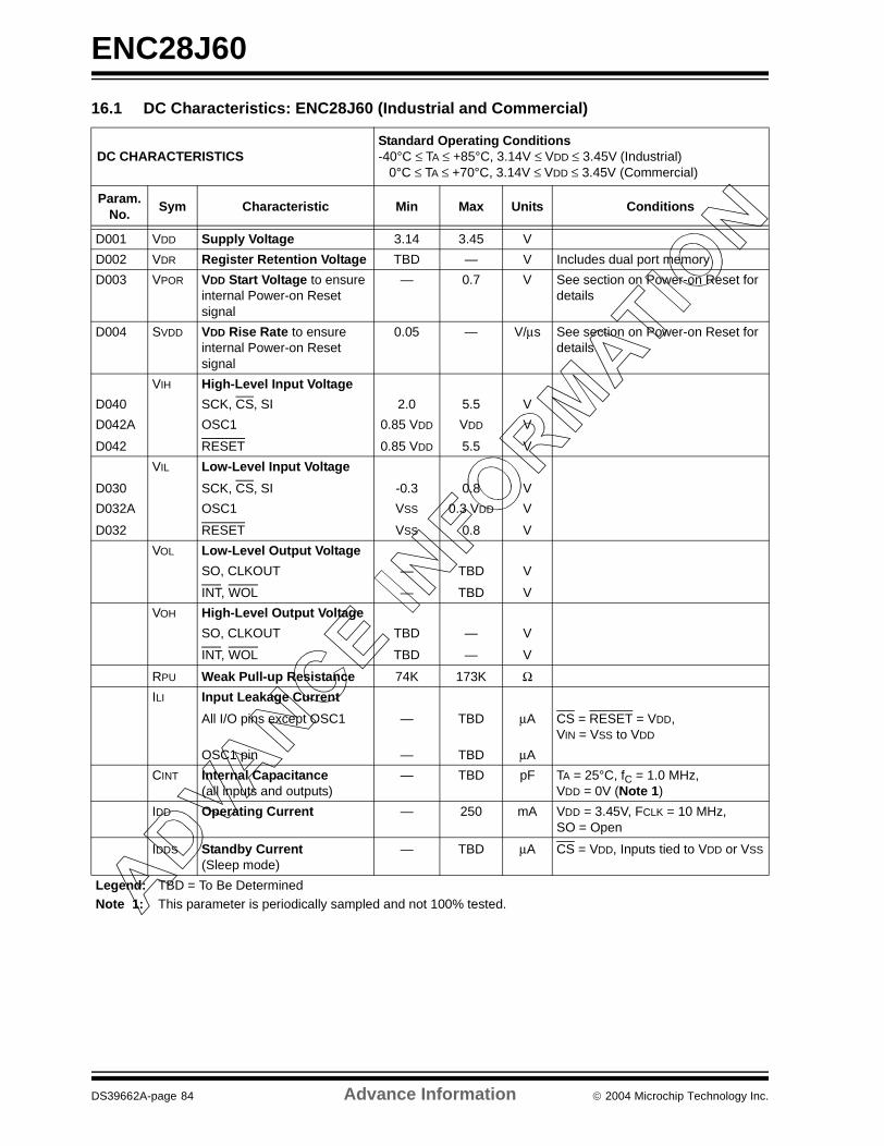
ENC28J60
16.1 DC Characteristics: ENC28J60 (Industrial and Commercial)
DC CHARACTERISTICSStandard Operating Conditions-40°C ≤ TA ≤ +85°C, 3.14V ≤ VDD ≤ 3.45V (Industrial) 0°C ≤ TA ≤ +70°C, 3.14V ≤ VDD ≤ 3.45V (Commercial)
Param.No.
Sym Characteristic Min Max Units Conditions
D001 VDD Supply Voltage 3.14 3.45 V
D002 VDR Register Retention Voltage TBD — V Includes dual port memory
D003 VPOR VDD Start Voltage to ensure internal Power-on Reset signal
— 0.7 V See section on Power-on Reset for details
D004 SVDD VDD Rise Rate to ensure internal Power-on Reset signal
0.05 — V/µs See section on Power-on Reset for details
VIH High-Level Input Voltage
D040 SCK, CS, SI 2.0 5.5 V
D042A OSC1 0.85 VDD VDD V
D042 RESET 0.85 VDD 5.5 V
VIL Low-Level Input Voltage
D030 SCK, CS, SI -0.3 0.8 V
D032A OSC1 VSS 0.3 VDD V
D032 RESET VSS 0.8 V
VOL Low-Level Output Voltage
SO, CLKOUT — TBD V
INT, WOL — TBD V
VOH High-Level Output Voltage
SO, CLKOUT TBD — V
INT, WOL TBD — V
RPU Weak Pull-up Resistance 74K 173K ΩILI Input Leakage Current
All I/O pins except OSC1 — TBD µA CS = RESET = VDD, VIN = VSS to VDD
OSC1 pin — TBD µA
CINT Internal Capacitance(all inputs and outputs)
— TBD pF TA = 25°C, fC = 1.0 MHz,VDD = 0V (Note 1)
IDD Operating Current — 250 mA VDD = 3.45V, FCLK = 10 MHz, SO = Open
IDDS Standby Current (Sleep mode)
— TBD µA CS = VDD, Inputs tied to VDD or VSS
Legend: TBD = To Be DeterminedNote 1: This parameter is periodically sampled and not 100% tested.
DS39662A-page 84 Advance Information 2004 Microchip Technology Inc.
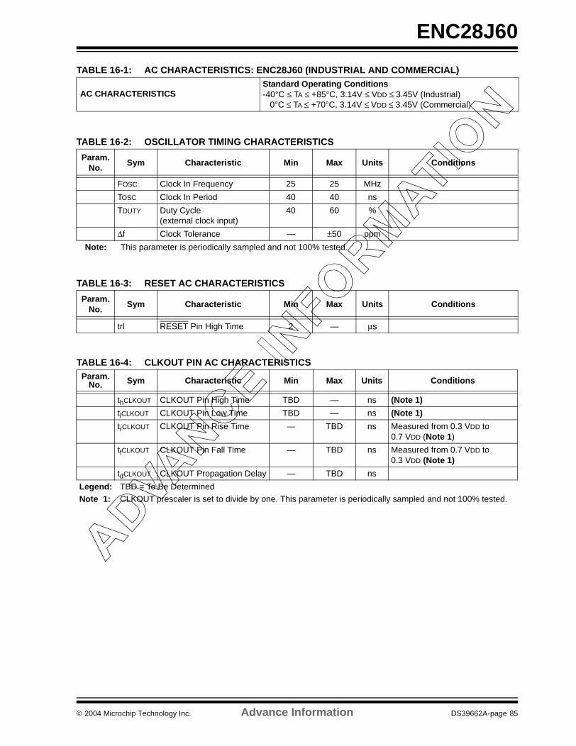
ENC28J60
TABLE 16-1: AC CHARACTERISTICS: ENC28J60 (INDUSTRIAL AND COMMERCIAL)
TABLE 16-2: OSCILLATOR TIMING CHARACTERISTICS
TABLE 16-3: RESET AC CHARACTERISTICS
TABLE 16-4: CLKOUT PIN AC CHARACTERISTICS
AC CHARACTERISTICSStandard Operating Conditions-40°C ≤ TA ≤ +85°C, 3.14V ≤ VDD ≤ 3.45V (Industrial) 0°C ≤ TA ≤ +70°C, 3.14V ≤ VDD ≤ 3.45V (Commercial)
Param.No.
Sym Characteristic Min Max Units Conditions
FOSC Clock In Frequency 25 25 MHz
TOSC Clock In Period 40 40 ns
TDUTY Duty Cycle (external clock input)
40 60 %
∆f Clock Tolerance — ±50 ppm
Note: This parameter is periodically sampled and not 100% tested.
Param.No.
Sym Characteristic Min Max Units Conditions
trl RESET Pin High Time 2 — µs
Param.No. Sym Characteristic Min Max Units Conditions
thCLKOUT CLKOUT Pin High Time TBD — ns (Note 1)
tlCLKOUT CLKOUT Pin Low Time TBD — ns (Note 1)
trCLKOUT CLKOUT Pin Rise Time — TBD ns Measured from 0.3 VDD to 0.7 VDD (Note 1)
tfCLKOUT CLKOUT Pin Fall Time — TBD ns Measured from 0.7 VDD to 0.3 VDD (Note 1)
tdCLKOUT CLKOUT Propagation Delay — TBD ns
Legend: TBD = To Be Determined
Note 1: CLKOUT prescaler is set to divide by one. This parameter is periodically sampled and not 100% tested.
2004 Microchip Technology Inc. Advance Information DS39662A-page 85

ENC28J60
TABLE 16-5: REQUIREMENTS FOR EXTERNAL MAGNETICS
TABLE 16-6: SPI™ INTERFACE AC CHARACTERISTICS
Parameter Min Norm Max Units Conditions
RX Turns Ratio — 1:1 — —
TX Turns Ratio — 1:1 — — Transformer Center Tap = 3.3V
Insertion Loss 0.0 0.6 1.1 dB
Primary Inductance 350 — — µH 8 mA bias
Transformer Isolation — 1.5 — kV
Differential to Common Mode Rejection
40 — — dB 0.1 to 10 MHz
Return Loss -16 — — dB
Param.No.
Sym Characteristic Min Max Units Conditions
FCLK Clock Frequency DC 10 MHz
1 TCSS CS Setup Time 100 — ns
2 TCSH CS Hold Time 100 — ns
3 TCSD CS Disable Time 100 — ns
4 TSU Data Setup Time 2 — ns
5 THD Data Hold Time 10 — ns
6 TR Clock Rise Time — TBD µs (Note 1)
7 TF Clock Fall Time — TBD µs (Note 1)
8 THI Clock High Time TBD — ns
9 TLO Clock Low Time TBD — ns
10 TV Output Valid from Clock Low — TBD ns
11 TDIS Output Disable Time — TBD ns (Note 1)
Legend: TBD = To Be DeterminedNote 1: This parameter is not 100% tested.
DS39662A-page 86 Advance Information 2004 Microchip Technology Inc.
ENC28J60
FIGURE 16-1: SPI™ INPUT TIMING
FIGURE 16-2: SPI™ OUTPUT TIMING
CS
SCK
SI
SO
TCSS
THDTSU
TFTR
TCSD
LSB InMSB In
High-Impedance
CS
SCK
SO
THI
MSB Out LSB Out
TCSH
TDIS
Don’t CareSI
TLO
TV
2004 Microchip Technology Inc. Advance Information DS39662A-page 87

ENC28J60
NOTES:
DS39662A-page 88 Advance Information 2004 Microchip Technology Inc.
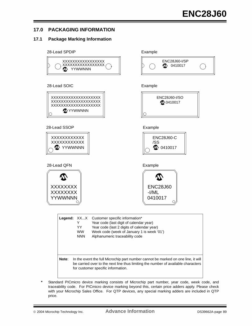
ENC28J60
17.0 PACKAGING INFORMATION
17.1 Package Marking Information
28-Lead SPDIP
XXXXXXXXXXXXXXXXXXXXXXXXXXXXXXXXXX
YYWWNNN
Example
ENC28J60-I/SP0410017
28-Lead SOIC
XXXXXXXXXXXXXXXXXXXXXXXXXXXXXXXXXXXXXXXXXXXXXXXXXXXXXXXXXXXX
YYWWNNN
Example
ENC28J60-I/SO0410017
28-Lead QFN
XXXXXXXXXXXXXXXXYYWWNNN
Example
ENC28J60-I/ML0410017
28-Lead SSOP
XXXXXXXXXXXXXXXXXXXXXXXX
YYWWNNN
Example
ENC28J60-C/SS
0410017
Legend: XX...X Customer specific information*Y Year code (last digit of calendar year)YY Year code (last 2 digits of calendar year)WW Week code (week of January 1 is week ‘01’)NNN Alphanumeric traceability code
Note: In the event the full Microchip part number cannot be marked on one line, it willbe carried over to the next line thus limiting the number of available charactersfor customer specific information.
* Standard PICmicro device marking consists of Microchip part number, year code, week code, andtraceability code. For PICmicro device marking beyond this, certain price adders apply. Please checkwith your Microchip Sales Office. For QTP devices, any special marking adders are included in QTPprice.
2004 Microchip Technology Inc. Advance Information DS39662A-page 89

ENC28J60
17.2 Package Details
The following sections give the technical details of the packages.
28-Lead Skinny Plastic Dual In-line (SP) – 300 mil Body (PDIP)
1510515105βMold Draft Angle Bottom
1510515105αMold Draft Angle Top
10.928.898.13.430.350.320eBOverall Row Spacing §
0.560.480.41.022.019.016BLower Lead Width
1.651.331.02.065.053.040B1Upper Lead Width
0.380.290.20.015.012.008cLead Thickness
3.433.303.18.135.130.125LTip to Seating Plane
35.1834.6734.161.3851.3651.345DOverall Length
7.497.246.99.295.285.275E1Molded Package Width
8.267.877.62.325.310.300EShoulder to Shoulder Width
0.38.015A1Base to Seating Plane
3.433.303.18.135.130.125A2Molded Package Thickness
4.063.813.56.160.150.140ATop to Seating Plane
2.54.100pPitch
2828nNumber of Pins
MAXNOMMINMAXNOMMINDimension Limits
MILLIMETERSINCHES*Units
2
1
D
n
E1
c
eB
β
E
α
p
L
A2
B
B1
A
A1
Notes:
JEDEC Equivalent: MO-095Drawing No. C04-070
* Controlling Parameter
Dimension D and E1 do not include mold flash or protrusions. Mold flash or protrusions shall not exceed .010” (0.254mm) per side.
§ Significant Characteristic
DS39662A-page 90 Advance Information 2004 Microchip Technology Inc.

ENC28J60
28-Lead Plastic Small Outline (SO) – Wide, 300 mil Body (SOIC)
Foot Angle Top φ 0 4 8 0 4 8
1512015120βMold Draft Angle Bottom1512015120αMold Draft Angle Top
0.510.420.36.020.017.014BLead Width0.330.280.23.013.011.009cLead Thickness
1.270.840.41.050.033.016LFoot Length0.740.500.25.029.020.010hChamfer Distance
18.0817.8717.65.712.704.695DOverall Length7.597.497.32.299.295.288E1Molded Package Width
10.6710.3410.01.420.407.394EOverall Width0.300.200.10.012.008.004A1Standoff §2.392.312.24.094.091.088A2Molded Package Thickness2.642.502.36.104.099.093AOverall Height
1.27.050pPitch2828nNumber of Pins
MAXNOMMINMAXNOMMINDimension LimitsMILLIMETERSINCHES*Units
21
D
p
n
B
E
E1
L
c
β
45°
h
φ
A2
α
A
A1
* Controlling Parameter
Notes:Dimensions D and E1 do not include mold flash or protrusions. Mold flash or protrusions shall not exceed .010” (0.254mm) per side.JEDEC Equivalent: MS-013Drawing No. C04-052
§ Significant Characteristic
2004 Microchip Technology Inc. Advance Information DS39662A-page 91
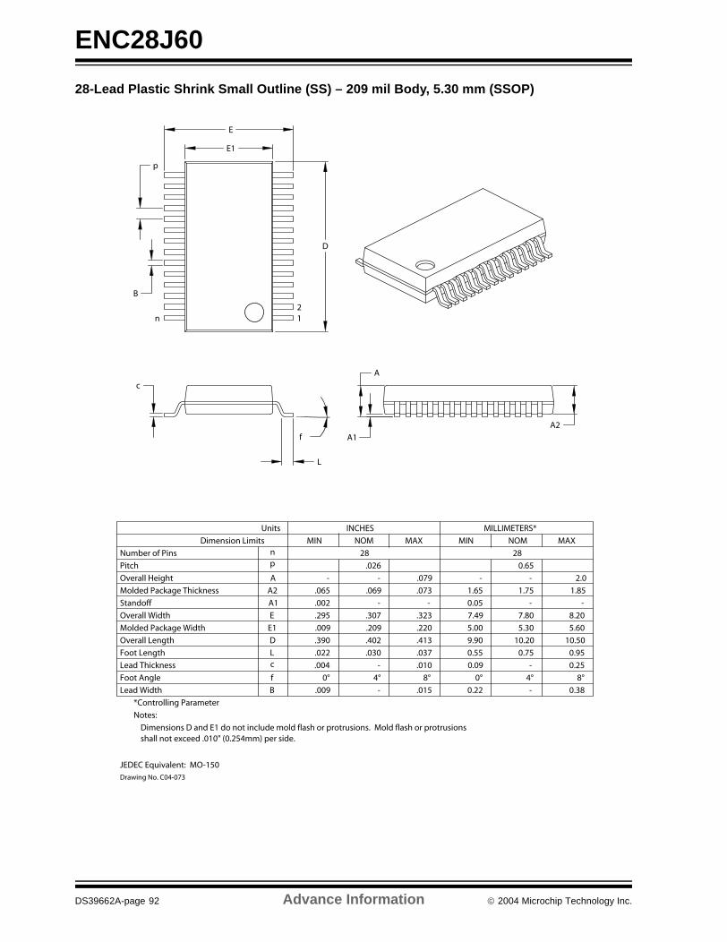
ENC28J60
28-Lead Plastic Shrink Small Outline (SS) – 209 mil Body, 5.30 mm (SSOP)
0.38-0.22.015-.009BLead Width
8°4°0°8°4°0°fFoot Angle
0.25-0.09.010-.004cLead Thickness
0.950.750.55.037.030.022LFoot Length
10.5010.209.90.413.402.390DOverall Length
5.605.305.00.220.209.009E1Molded Package Width
8.207.807.49.323.307.295EOverall Width
--0.05--.002A1Standoff
1.851.751.65.073.069.065A2Molded Package Thickness
2.0--.079--AOverall Height
0.65.026pPitch
2828nNumber of Pins
MAXNOMMINMAXNOMMINDimension Limits
MILLIMETERS*INCHESUnits
21
D
p
n
B
E1
E
L
c
fA2
A1
A
shall not exceed .010" (0.254mm) per side.Dimensions D and E1 do not include mold flash or protrusions. Mold flash or protrusions
Notes:
JEDEC Equivalent: MO-150Drawing No. C04-073
*Controlling Parameter
DS39662A-page 92 Advance Information 2004 Microchip Technology Inc.

ENC28J60
28-Lead Plastic Quad Flat No Lead Package (ML) 6x6 mm Body (QFN) – With 0.55 mm Contact Length (Saw Singulated)
Contact Width
*Controlling Parameter
Drawing No. C04-105
Notes:
JEDEC equivalent: MO-220
b .009 .011 .013 0.23 0.28 0.33
Pitch
Number of Pins
Overall Width
Standoff
Overall Length
Overall Height
MAX
Units
Dimension Limits
A1
D
E
n
e
A
.000
INCHES
.026 BSC
MIN
28
NOM MAX
.002 0.00
6.00
MILLIMETERS*
.039
MIN
28
0.65 BSC
NOM
0.05
1.000.90.035
.001 0.02
Contact Length L .020 .024 .028 0.50 0.60 0.70
E2
D2
Exposed Pad Width
Exposed Pad Length
.140 .146 .152 3.55 3.70 3.85
.031 0.80
5.90 6.10.240.236.232
.232 .236 6.00.240 5.90 6.10
.140 .146 3.70.152 3.55 3.85
b
D2D
PAD OUTLINEALTERNATE
SEE DETAIL
A1
A
DETAIL
TOP VIEW
OPTIONALINDEXAREA
1
2
L
BOTTOM VIEW
n
E
METALPAD
ALTERNATE
EXPOSED
INDICATORSINDEX
e
E2
Revised 05-24-04
Contact Thickness A3 .008 REF 0.20 REF
2004 Microchip Technology Inc. Advance Information DS39662A-page 93

ENC28J60
NOTES:
DS39662A-page 94 Advance Information 2004 Microchip Technology Inc.

ENC28J60
INDEX
BBlock Diagrams
Crystal Oscillator Operation .......................................... 5ENC28J60 Architecture ................................................ 3Ethernet Buffer Organization ...................................... 18Ethernet Packet Format .............................................. 31External Clock Source .................................................. 5External Connections.................................................... 7I/O Level Shifting
3-State Buffers...................................................... 8AND Gate ............................................................. 8
Interrupt Logic ............................................................. 65LEDB Polarity Configuration ......................................... 8Memory Organization.................................................. 11On-Chip Reset Circuit ................................................. 59Typical Interface............................................................ 4
Broadcast Filter ................................................................... 52Built-in Self-Test Controller ................................................. 79
Address Fill Mode ....................................................... 80Associated Registers .................................................. 81EBSTCS registers....................................................... 80EBSTSD Register ....................................................... 80Pattern Shift Fill Mode................................................. 81Random Data Fill Mode .............................................. 80Random Data Fill with Race Mode ............................. 80Use.............................................................................. 80
CChecksum Calculations ...................................................... 76CLKOUT Pin ......................................................................... 6Control Register Map .......................................................... 12Control Register Summary............................................ 13–14Control Registers ................................................................ 12
DDMA Controller ................................................................... 75
Access to Buffers ........................................................ 17Associated Registers .................................................. 76Checksum Calculations .............................................. 76Copying Memory......................................................... 75
Duplex-ModeConfiguation and Negotiation...................................... 53
EElectrical Characteristics..................................................... 83
Absolute Maximum Ratings ........................................ 83AC Characteristics ...................................................... 85CLKOUT Pin AC ......................................................... 85DC Characteristics ...................................................... 84Oscillator Timing ......................................................... 85Requirements for External Magnetics......................... 86Reset AC..................................................................... 85SPI Interface AC ......................................................... 86
ENC28J60 Block Diagram .................................................... 3EREVID Register ................................................................ 22Errata .................................................................................... 2Ethernet Buffer .................................................................... 17
Organization (Diagram)............................................... 18Ethernet Overview .............................................................. 31External Connections (Diagram)........................................... 7
FFiltering
Using AND Logic ........................................................ 50Using OR Logic .......................................................... 49
Flow Control........................................................................ 55Associated Registers.................................................. 57Full-Duplex Mode ....................................................... 55Half-Duplex Mode....................................................... 55Sample Full-Duplex Network (Diagram) ..................... 55
Full-Duplex-ModeOperation.................................................................... 53
HHalf-Duplex-Mode
Operation.................................................................... 53Hash Table Filter ................................................................ 52
II/O Level Shifting .................................................................. 8
Using 3-State Buffers ................................................... 8Using AND Gates ......................................................... 8
Initialization......................................................................... 33MAC Settings.............................................................. 34PHY Settings .............................................................. 38Receive Buffer ............................................................ 33Receive Filters............................................................ 33Transmit Buffer ........................................................... 33Waiting for OST .......................................................... 33
Interrupts ............................................................................ 65DMA Flag (DMAIF) ..................................................... 71INT Enable (INTIE) ..................................................... 66Link Change Flag (LINKIF)......................................... 71Receive Error Flag (RXERIF) ..................................... 70Receive Packet Pending Flag (PKTIF) ....................... 71Transmit Error Flag (TXERIF) .................................... 70Transmit Interrupt Flag (TXIF) .................................... 70WOL Interrupts ........................................................... 71
LLED Configuration ................................................................ 8LEDB Polarity and Reset Configuration................................ 8
MMagic Packet Filter ............................................................. 52Magnetics and External Components................................... 7Memory Organization ......................................................... 11Multicast Filter..................................................................... 52
OOscillator............................................................................... 5
CLKOUT Transition ...................................................... 6Crystal Oscillator .......................................................... 5External Clock Source .................................................. 5Start-up Timer............................................................... 5
PPackaging Information........................................................ 89
Details......................................................................... 90Marking....................................................................... 89
2004 Microchip Technology Inc. Advance Information DS39662A-page 95

ENC28J60
Packet Format..................................................................... 31CRC Field ................................................................... 32Data Field.................................................................... 32Destination Address.................................................... 32Padding Field .............................................................. 32Preamble/Start-of-Frame Delimiter ............................. 31Source Address .......................................................... 32Type/Length Field ....................................................... 32
Pattern Match Filter............................................................. 51Per Packet Control Byte Format ......................................... 39PHID Registers ................................................................... 22PHSTAT Registers.............................................................. 22PHY Register Summary ...................................................... 20PHY Registers..................................................................... 19
Reading....................................................................... 19Scanning ..................................................................... 19Writing......................................................................... 19
Pinout Diagrams.................................................................... 1Pinout I/O Descriptions ......................................................... 4Power-Down........................................................................ 77
Associated Registers .................................................. 77Power-on Reset (POR) ....................................................... 60
RRead Control Register (RCR) ............................................. 27Reading and Writing to Buffers ........................................... 17Receive Buffer..................................................................... 17Receive Filters .................................................................... 47
Broadcast .................................................................... 52Hash Table.................................................................. 52Magic Packet .............................................................. 52Multicast ...................................................................... 52Pattern Match.............................................................. 51Unicast ........................................................................ 51Using AND Logic......................................................... 50Using OR Logic........................................................... 49
Receive Only Reset ............................................................ 60Receiving Packets............................................................... 43
Associated Registers .................................................. 46Calculating Buffer Free Space .................................... 45Calculating Free Receive Buffer Space ...................... 45Calculating Random Access Address......................... 44Freeing Buffer Space .................................................. 45Reading....................................................................... 44Sample Packet Layout ................................................ 43Status Vectors............................................................. 44
RegistersEBSTCON (Self-Test Control) .................................... 79ECOCON (Clock Output Control) ................................. 6ECON1 (Ethernet Control 1) ....................................... 15ECON2 (Ethernet Control 2) ....................................... 16EFLOCON (Ethernet Flow Control) ............................ 56EIE (Ethernet Interrupt Enable)................................... 67EIR (Ethernet Interrupt Request - Flag) ...................... 68ERXFCON (Receive Filter Control) ............................ 48ESTAT (Ethernet Status) ............................................ 66EWOLIE (Ethernet Wake-up on
LAN Interrupt Enable) ......................................... 72EWOLIR (Ethernet Wake-up on
LAN Interrupt Request - Flag)............................. 73MABBIPG (MAC Back-to-Back
Inter-Packet Gap)................................................ 37MACON1 (MAC Control 1).......................................... 34MACON2 (MAC Control 2).......................................... 61
MACON3 (MAC Control 3) ......................................... 35MACON4 (MAC Control 4) ......................................... 36MAPHSUP (MAC-PHY Support) ................................ 62MICON (MII Control)................................................... 21MISTAT (MII Status) ................................................... 22PHCON1 (PHY Control 1) .......................................... 63PHCON2 (PHY Control 2) .......................................... 38PHID (PHY Device ID)................................................ 22PHIE (PHY Interrupt Enable) ...................................... 69PHIR (PHY Interrupt Request - Flag) ......................... 69PHLCON (PHY Module LED Control)........................... 9PHSTAT1 (Physical Layer Status 1)........................... 23PHSTAT2 (Physical Layer Status 2)........................... 24
Reset .................................................................................. 59MAC and PHY Subsystem Resets ............................. 61Power-on Reset .......................................................... 60Receive Only Reset .................................................... 60System Reset ............................................................. 60Transmit Only Reset ................................................... 60
SSerial Peripheral Interface. See SPI.SPI
Bit Field Clear Command............................................ 29Bit Field Set Command............................................... 29Instruction Set............................................................. 26Overview..................................................................... 25Read Buffer Memory Command................................. 28Read Control Register Command............................... 27System Command ...................................................... 30Write Buffer Memory Command ................................. 29Write Control Register Command............................... 28
SPI.System Reset ..................................................................... 60
TTermination Requirement ..................................................... 7Timing Diagrams
CLKOUT Transition ...................................................... 6Read Control Register Command
Sequence (ETH)................................................. 27Read Control Register Command
Sequence (MAC/MII) .......................................... 27SPI Input ..................................................................... 87SPI Input Timing ......................................................... 25SPI Output .................................................................. 87SPI Output Timing ...................................................... 25System Command Sequence ..................................... 30Write Buffer Memory Command Sequence ................ 29Write Control Register Command Sequence.............. 28
Transmit Buffer ................................................................... 17Transmit Only Reset ........................................................... 60Transmitting Packets .......................................................... 39
Associated Registers .................................................. 42Sample Packet Layout................................................ 40Status Vectors ............................................................ 41
Typical ENC28J60-Based Interface...................................... 4
UUnicast Filter....................................................................... 51
WWake-up on LAN (WOL)..................................................... 71WWW, On-Line Support ....................................................... 2
DS39662A-page 96 Advance Information 2004 Microchip Technology Inc.

ENC28J60
ON-LINE SUPPORT
Microchip provides on-line support on the MicrochipWorld Wide Web site.
The web site is used by Microchip as a means to makefiles and information easily available to customers. Toview the site, the user must have access to the Internetand a web browser, such as Netscape® or Microsoft®
Internet Explorer. Files are also available for FTPdownload from our FTP site.
Connecting to the Microchip Internet Web Site
The Microchip web site is available at the followingURL:
www.microchip.com
The file transfer site is available by using an FTPservice to connect to:
ftp://ftp.microchip.com
The web site and file transfer site provide a variety ofservices. Users may download files for the latestDevelopment Tools, Data Sheets, Application Notes,User's Guides, Articles and Sample Programs. A vari-ety of Microchip specific business information is alsoavailable, including listings of Microchip sales offices,distributors and factory representatives. Other dataavailable for consideration is:
• Latest Microchip Press Releases• Technical Support Section with Frequently Asked
Questions • Design Tips
• Device Errata• Job Postings• Microchip Consultant Program Member Listing
• Links to other useful web sites related to Microchip Products
• Conferences for products, Development Systems, technical information and more
• Listing of seminars and events
SYSTEMS INFORMATION AND UPGRADE HOT LINE
The Systems Information and Upgrade Line providessystem users a listing of the latest versions of all ofMicrochip's development systems software products.Plus, this line provides information on how customerscan receive the most current upgrade kits. The Hot LineNumbers are:
1-800-755-2345 for U.S. and most of Canada, and
1-480-792-7302 for the rest of the world.
042003
2004 Microchip Technology Inc. Advance Information DS39662A-page 97

ENC28J60
READER RESPONSE
It is our intention to provide you with the best documentation possible to ensure successful use of your Microchip prod-uct. If you wish to provide your comments on organization, clarity, subject matter, and ways in which our documentationcan better serve you, please FAX your comments to the Technical Publications Manager at (480) 792-4150.
Please list the following information, and use this outline to provide us with your comments about this document.
To: Technical Publications Manager
RE: Reader Response
Total Pages Sent ________
From: Name
Company
Address
City / State / ZIP / Country
Telephone: (_______) _________ - _________
Application (optional):
Would you like a reply? Y N
Device: Literature Number:
Questions:
FAX: (______) _________ - _________
DS39662AENC28J60
1. What are the best features of this document?
2. How does this document meet your hardware and software development needs?
3. Do you find the organization of this document easy to follow? If not, why?
4. What additions to the document do you think would enhance the structure and subject?
5. What deletions from the document could be made without affecting the overall usefulness?
6. Is there any incorrect or misleading information (what and where)?
7. How would you improve this document?
DS39662A-page 98 Advance Information 2004 Microchip Technology Inc.

2004 Microchip Technology Inc. Advance Information DS39662A-page 99
ENC28J60
PRODUCT IDENTIFICATION SYSTEM
To order or obtain information, e.g., on pricing or delivery, refer to the factory or the listed sales office.
PART NO. -X /XX
PackageTemperatureRange
Device
Device ENC28J60: Ethernet Controller w/SPI™ InterfaceENC28J60T: Ethernet Controller w/SPI™ Interface
(Tape and Reel)
Temperature Range
I = -40°C to +85°C (Industrial)(SPDIP, SOIC and QFN packages only)
C = 0°C to +70°C (Commercial)(SSOP packages only)
Package SP = SPDIP (Skinny Plastic DIP)SO = SOIC (Plastic Small Outline)SS = SSOP (Plastic Shrink Small Outline)ML = QFN (Quad Flat No Lead)
Examples:
a) ENC28J60-I/SP: Industrial temperature, SPDIP package.
b) ENC28J60-I/SO: Industrial temperature, SOIC package.
c) ENC28J60T-I/SO: Tape and Reel, Industrialtemperature, SOIC package.
d) ENC28J60-C/SS: Commercial temperature,SSOP package.
e) ENC28J60T-C/SS: Tape and Reel, Comercial temperature, SSOP package.
f) ENC28J60-I/ML: Industrial temperature, QFN package.

DS39662A-page 100 Advance Information 2004 Microchip Technology Inc.
AMERICASCorporate Office2355 West Chandler Blvd.Chandler, AZ 85224-6199Tel: 480-792-7200 Fax: 480-792-7277Technical Support: http://support.microchip.comWeb Address: www.microchip.com
AtlantaAlpharetta, GA Tel: 770-640-0034 Fax: 770-640-0307
BostonWestford, MA Tel: 978-692-3848 Fax: 978-692-3821
ChicagoItasca, IL Tel: 630-285-0071 Fax: 630-285-0075
DallasAddison, TX Tel: 972-818-7423 Fax: 972-818-2924
DetroitFarmington Hills, MI Tel: 248-538-2250Fax: 248-538-2260
KokomoKokomo, IN Tel: 765-864-8360Fax: 765-864-8387
Los AngelesMission Viejo, CA Tel: 949-462-9523 Fax: 949-462-9608
San JoseMountain View, CA Tel: 650-215-1444Fax: 650-961-0286
TorontoMississauga, Ontario, CanadaTel: 905-673-0699 Fax: 905-673-6509
ASIA/PACIFICAustralia - SydneyTel: 61-2-9868-6733 Fax: 61-2-9868-6755
China - BeijingTel: 86-10-8528-2100 Fax: 86-10-8528-2104
China - ChengduTel: 86-28-8676-6200 Fax: 86-28-8676-6599
China - FuzhouTel: 86-591-8750-3506 Fax: 86-591-8750-3521
China - Hong Kong SARTel: 852-2401-1200 Fax: 852-2401-3431
China - ShanghaiTel: 86-21-5407-5533 Fax: 86-21-5407-5066China - ShenyangTel: 86-24-2334-2829Fax: 86-24-2334-2393
China - ShenzhenTel: 86-755-8203-2660 Fax: 86-755-8203-1760
China - ShundeTel: 86-757-2839-5507 Fax: 86-757-2839-5571
China - QingdaoTel: 86-532-502-7355 Fax: 86-532-502-7205
ASIA/PACIFICIndia - BangaloreTel: 91-80-2229-0061 Fax: 91-80-2229-0062
India - New DelhiTel: 91-11-5160-8631Fax: 91-11-5160-8632
Japan - KanagawaTel: 81-45-471- 6166 Fax: 81-45-471-6122
Korea - SeoulTel: 82-2-554-7200 Fax: 82-2-558-5932 or 82-2-558-5934
SingaporeTel: 65-6334-8870 Fax: 65-6334-8850
Taiwan - KaohsiungTel: 886-7-536-4818Fax: 886-7-536-4803
Taiwan - TaipeiTel: 886-2-2500-6610 Fax: 886-2-2508-0102
Taiwan - HsinchuTel: 886-3-572-9526Fax: 886-3-572-6459
EUROPEAustria - WeisTel: 43-7242-2244-399Fax: 43-7242-2244-393Denmark - BallerupTel: 45-4450-2828 Fax: 45-4485-2829
France - MassyTel: 33-1-69-53-63-20 Fax: 33-1-69-30-90-79
Germany - IsmaningTel: 49-89-627-144-0 Fax: 49-89-627-144-44
Italy - Milan Tel: 39-0331-742611 Fax: 39-0331-466781
Netherlands - DrunenTel: 31-416-690399 Fax: 31-416-690340
England - BerkshireTel: 44-118-921-5869Fax: 44-118-921-5820
WORLDWIDE SALES AND SERVICE
10/20/04