elmore delay, logical effort. modern interconnect © rabaey, ch4wire.ppt, slide 22
TRANSCRIPT

Elmore Delay, Logical Effort

Modern Interconnect
© Rabaey, ch4Wire.ppt, slide 22

Example: Intel 0.25 micron Process
5 metal layersTi/Al - Cu/Ti/TiNPolysilicon dielectric
© Rabaey, ch4Wire.ppt, slide 23

Modern Interconnect• 90nm process
© Chris Kim (image from Intel?)

The Lumped RC-Model, The Elmore Delay
© Rabaey, ch4Wire.ppt, slide 27
(result *0.69)

Example: The Elmore Delay
Shared Paths:
R44 = R1+R3+R4
Rii = R1+R3+Ri
Ri4 = R1+R3
Ri2 = R1
Ti = C1R1 + C2R1 + C3(R1+R3) + C4(R1+R3) + Ci(R1+R3+Ri)

The Elmore Delay RC Chain
© Rabaey, ch4Wire.ppt

The Distributed RC-line
© Rabaey, ch4Wire.ppt
Diffusion Equation
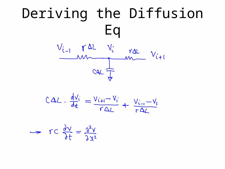
Deriving the Diffusion Eq

Step-response of RC wire as a function of time and space
0 0.5 1 1.5 2 2.5 3 3.5 4 4.5 50
0.5
1
1.5
2
2.5
time (nsec)
volta
ge (V
)
x= L/10
x = L/4
x = L/2
x= L
© Rabaey, ch4Wire.ppt

RC-Models
© Rabaey, ch4Wire.ppt

Driving an RC-line
Vi n
Rs Vo ut
(rw,cw,L)
© Rabaey, ch4Wire.ppt

Designing Fast CMOS Gates
Slides from chapter6.ppt of Rabaey’s page

EE141© Digital Integrated Circuits2ndCombinational Circuits
Fan-In ConsiderationsFan-In Considerations
DCBA
D
C
B
A CL
C3
C2
C1
Distributed RC model (Elmore delay)
tpHL = 0.69 Reqn(C1+2C2+3C3+4CL)
Propagation delay deteriorates rapidly as a function of fan-in – quadratically in the worst case.

EE141© Digital Integrated Circuits2ndCombinational Circuits
ttpp as a Function of Fan-In as a Function of Fan-In
tpLH
t p (
pse
c)
fan-in
Gates with a fan-in greater than 4 should be avoided.
0
250
500
750
1000
1250
2 4 6 8 10 12 14 16
tpHL
quadratic
linear
tp

EE141© Digital Integrated Circuits2ndCombinational Circuits
ttpp as a Function of Fan-In and Fan-Out as a Function of Fan-In and Fan-Out
Fan-in: quadratic due to increasing resistance and capacitance
Fan-out: each additional fan-out gate adds two gate capacitances to CL
tp = a1FI + a2FI2 + a3FO

EE141© Digital Integrated Circuits2ndCombinational Circuits
Fast Complex Gates:Fast Complex Gates:Design Technique 1Design Technique 1 Transistor sizing
as long as fan-out capacitance dominates Progressive sizing
InN CL
C3
C2
C1In1
In2
In3
M1
M2
M3
MNDistributed RC line
M1 > M2 > M3 > … > MN (the fet closest to the output is the smallest)
Can reduce delay by more than 20%; decreasing gains as technology shrinks

EE141© Digital Integrated Circuits2ndCombinational Circuits
Fast Complex Gates:Fast Complex Gates:Design Technique 2Design Technique 2
Transistor ordering
C2
C1In1
In2
In3
M1
M2
M3 CL
C2
C1In3
In2
In1
M1
M2
M3 CL
critical path critical path
charged1
01charged
charged1
delay determined by time to discharge CL, C1 and C2
delay determined by time to discharge CL
1
1
01 charged
discharged
discharged

EE141© Digital Integrated Circuits2ndCombinational Circuits
Fast Complex Gates:Fast Complex Gates:Design Technique 3Design Technique 3
Alternative logic structures
F = ABCDEFGH

EE141© Digital Integrated Circuits2ndCombinational Circuits
Fast Complex Gates:Fast Complex Gates:Design Technique 4Design Technique 4
Isolating fan-in from fan-out using buffer insertion
CLCL

Logical Effort
Slides from chapter6.ppt of Rabaey’s page

EE141© Digital Integrated Circuits2ndCombinational Circuits
Transistor SizingTransistor Sizing
Cg=Cg=
Cg=Cint=
Cint=Cint=
D=1+f D=2+4/3 f D=2+5/3 f


Normalized Space

Parasitic Term P
NOTE: p is a gate parameter function(W)

Logical Effort Term g
NOTE: g is a gate parameter function(W)

EE141© Digital Integrated Circuits2ndCombinational Circuits
Transistor Sizing a Complex Transistor Sizing a Complex CMOS GateCMOS Gate
OUT = D + A • (B + C)
D
A
B C
D
A
B
C
1
2
2 2
4
4
8
8
6
3
6
6

EE141© Digital Integrated Circuits2ndCombinational Circuits
Logical EffortLogical Effort
From Sutherland, Sproull

EE141© Digital Integrated Circuits2ndCombinational Circuits
Logical Effort of GatesLogical Effort of Gates
IntrinsicDelay
EffortDelay
1 2 3 4 5
Fanoutf
1
2
3
4
5
Inverter:g =
1; p = 1
2-input N
AND:g =
4/3
;p =
2
No
rmal
ized
Del
ay

EE141© Digital Integrated Circuits2ndCombinational Circuits
ttpp as a Function of Fan-Out as a Function of Fan-Out
2 4 6 8 10 12 14 16
tpNOR2
t p (
pse
c)
eff. fan-out
All gates have the same drive current.
tpNAND2
tpINV
Slope is a function of “driving strength”

EE141© Digital Integrated Circuits2ndCombinational Circuits
Buffer ExampleBuffer Example
N
iiii fgpDelay
1
For given N: Ci+1/Ci = Ci/Ci-1
To find N: Ci+1/Ci ~ 4
How to generalize this to any logic path?
CL
In Out
1 2 N
(in units of inv)

EE141© Digital Integrated Circuits2ndCombinational Circuits
Delay in a Logic GateDelay in a Logic Gate
Gate delay:
d = h + p
effort delay intrinsic delay
Effort delay:
h = g f
logical effort
effective fanout = Cout/Cin
Logical effort is a function of topology, independent of sizingEffective fanout (electrical effort) is a function of load/gate size


EE141© Digital Integrated Circuits2ndCombinational Circuits
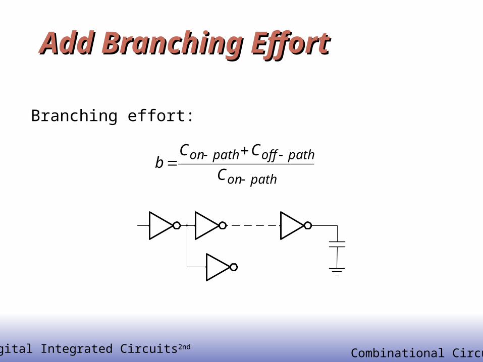
Add Branching EffortAdd Branching Effort
Branching effort:
pathon
pathoffpathon
C
CCb


EE141© Digital Integrated Circuits2ndCombinational Circuits
Multistage NetworksMultistage Networks
Stage effort: hi = gifi
Path electrical effort: F = Cout/Cin
Path logical effort: G = g1g2…gN
Branching effort: B = b1b2…bN
Path effort: H = GFB
Path delay D = di = pi + hi
N
iiii fgpDelay
1

EE141© Digital Integrated Circuits2ndCombinational Circuits
Optimum Effort per StageOptimum Effort per Stage
HhN
When each stage bears the same effort:
N Hh
PNHpfgD Niii /1ˆ
Minimum path delay
Effective fanout of each stage: ii ghf
Stage efforts: g1f1 = g2f2 = … = gNfN

EE141© Digital Integrated Circuits2ndCombinational Circuits
Optimal Number of StagesOptimal Number of Stages
For a given load, and given input capacitance of the first gateFind optimal number of stages and optimal sizing
invN NpNHD /1
0ln /1/1/1
invNNN pHHH
N
D
NHhˆ/1Substitute ‘best stage effort’

EE141© Digital Integrated Circuits2ndCombinational Circuits
Example: Optimize PathExample: Optimize Path
1a
b c
5
g = 1f = a
g = 5/3f = b/a
g = 5/3f = c/b
g = 1f = 5/c
Effective fanout, F = 5G =H =h =a =b =c =

EE141© Digital Integrated Circuits2ndCombinational Circuits
Example: Optimize PathExample: Optimize Path
1a
b c
5
g = 1f = a
g = 5/3f = b/a
g = 5/3f = c/b
g = 1f = 5/c
Effective fanout, F = 5G = 25/9H = 125/9 = 13.9h = 1.93a = 1.93b = ha/g2 = 2.23c = hb/g3 = 5g4/f = 2.59


EE141© Digital Integrated Circuits2ndCombinational Circuits
Example – 8-input ANDExample – 8-input AND

EE141© Digital Integrated Circuits2ndCombinational Circuits
Method of Logical EffortMethod of Logical Effort
Compute the path effort: F = GBH Find the best number of stages N ~ log4F Compute the stage effort f = F1/N
Sketch the path with this number of stages Work either from either end, find sizes:
Cin = Cout*g/f
Reference: Sutherland, Sproull, Harris, “Logical Effort, Morgan-Kaufmann 1999.

EE141© Digital Integrated Circuits2ndCombinational Circuits
SummarySummary
Sutherland,SproullHarris