electronics and optoelectronics xinming li, li tao, zefeng ... · 1department of electronic...
TRANSCRIPT

Graphene and related two-dimensional materials: Structure-property relationships forelectronics and optoelectronicsXinming Li, Li Tao, Zefeng Chen, Hui Fang, Xuesong Li, Xinran Wang, Jian-Bin Xu, and Hongwei Zhu
Citation: Applied Physics Reviews 4, 021306 (2017); doi: 10.1063/1.4983646View online: http://dx.doi.org/10.1063/1.4983646View Table of Contents: http://aip.scitation.org/toc/are/4/2Published by the American Institute of Physics
APPLIED PHYSICS REVIEWS
Graphene and related two-dimensional materials: Structure-propertyrelationships for electronics and optoelectronics
Xinming Li,1,a),b) Li Tao,1,b) Zefeng Chen,1,b) Hui Fang,2 Xuesong Li,3 Xinran Wang,4
Jian-Bin Xu,1,a) and Hongwei Zhu5,a)
1Department of Electronic Engineering, The Chinese University of Hong Kong, Hong Kong, China2Department of Electrical and Computer Engineering, Northeastern University, Boston, Massachusetts 02115,USA3State Key Laboratory of Electronic Thin Films and Integrated Devices and School of Microelectronics andSolid State Electronics, University of Electronic Science and Technology of China, Chengdu 610054, China4National Laboratory of Solid State Microstructures, School of Electronic Science and Engineering, andCollaborative Innovation Center of Advanced Microstructures, Nanjing University, Nanjing 210093, China5State Key Laboratory of New Ceramics and Fine Processing, School of Materials Science and Engineering,Tsinghua University, Beijing 100084, China
(Received 20 December 2016; accepted 3 May 2017; published online 6 June 2017)
The exfoliation and identification of the two-dimensional (2D) single atomic layer of carbon have
opened the opportunity to explore graphene and related 2D materials due to their unique properties.
2D materials are regarded as one of the most exciting solutions for next generation electronics and
optoelectronics in the technological evolution of semiconductor technology. In this review, we
focus on the core concept of “structure-property relationships” to explain the state-of-the-art of 2D
materials and summarize the unique electrical and light-matter interaction properties in 2D materi-
als. Based on this, we discuss and analyze the structural properties of 2D materials, such as defects
and dopants, the number of layers, composition, phase, strain, and other structural characteristics,
which could significantly alter the properties of 2D materials and hence affect the performance of
semiconductor devices. In particular, the building blocks principles and potential electronic and
optoelectronic applications based on 2D materials are explained and illustrated. Indeed, 2D materi-
als and related heterostructures offer the promise for challenging the existing technologies and
providing the chance to have social impact. More efforts are expected to propel this exciting field
forward. Published by AIP Publishing. [http://dx.doi.org/10.1063/1.4983646]
TABLE OF CONTENTS
I. INTRODUCTION . . . . . . . . . . . . . . . . . . . . . . . . . . . . 2
A. Two-dimensional (2D) material family . . . . . 2
B. 2D material tetrahedron . . . . . . . . . . . . . . . . . . 3
II. ELECTRONIC AND OPTICAL PROPERTIES . . 3
A. Electronic properties of graphene. . . . . . . . . . 3
1. Band structure . . . . . . . . . . . . . . . . . . . . . . . 4
2. Electron optics . . . . . . . . . . . . . . . . . . . . . . . 4
3. Electron transport . . . . . . . . . . . . . . . . . . . . 4
B. Light-matter interactions in graphene . . . . . . 5
C. Graphene plasmons . . . . . . . . . . . . . . . . . . . . . . 7
D. 2D semiconductors . . . . . . . . . . . . . . . . . . . . . . 7
1. Electronic properties . . . . . . . . . . . . . . . . . . 7
2. Optical properties . . . . . . . . . . . . . . . . . . . . 8
E. h-BN . . . . . . . . . . . . . . . . . . . . . . . . . . . . . . . . . . 9
III. SYNTHESIS AND PROCESSING . . . . . . . . . . . . 9
A. Top-down . . . . . . . . . . . . . . . . . . . . . . . . . . . . . . 9
B. Bottom-up. . . . . . . . . . . . . . . . . . . . . . . . . . . . . . 10
C. Transfer and assembly . . . . . . . . . . . . . . . . . . . 11
IV. STRUCTURAL MODIFICATIONS . . . . . . . . . . . 11
A. Defects . . . . . . . . . . . . . . . . . . . . . . . . . . . . . . . . 11
1. Point defects . . . . . . . . . . . . . . . . . . . . . . . . . 11
2. Line defects . . . . . . . . . . . . . . . . . . . . . . . . . 12
B. Dopants . . . . . . . . . . . . . . . . . . . . . . . . . . . . . . . . 13
1. Substitutional doping. . . . . . . . . . . . . . . . . . 13
2. Surface doping . . . . . . . . . . . . . . . . . . . . . . . 14
C. Alloying . . . . . . . . . . . . . . . . . . . . . . . . . . . . . . . 14
D. Phase transition . . . . . . . . . . . . . . . . . . . . . . . . . 15
E. Number of layers. . . . . . . . . . . . . . . . . . . . . . . . 15
F. Strain . . . . . . . . . . . . . . . . . . . . . . . . . . . . . . . . . . 16
G. Corrugations. . . . . . . . . . . . . . . . . . . . . . . . . . . . 18
V. BUILDING BLOCKS . . . . . . . . . . . . . . . . . . . . . . . . 18
A. Schottky junction . . . . . . . . . . . . . . . . . . . . . . . 19
1. Graphene-semiconductor contacts . . . . . . . 19
2. Metal-2D semiconductor contacts . . . . . . . 19
B. p-n junction . . . . . . . . . . . . . . . . . . . . . . . . . . . . 20
1. 2D-3D semiconductor heterostructures . . 20
a)Authors to whom correspondence should be addressed: xmli1015@gmail.
com; [email protected]; and [email protected])X. M. Li, L. Tao, and Z. F. Chen contributed equally to this work.
1931-9401/2017/4(2)/021306/31/$30.00 Published by AIP Publishing.4, 021306-1
APPLIED PHYSICS REVIEWS 4, 021306 (2017)
2. 2D-2D semiconductor vertical
heterostructures . . . . . . . . . . . . . . . . . . . . . . 20
3. 2D-2D semiconductor lateral
heterostructures . . . . . . . . . . . . . . . . . . . . . . 21
4. Homostructures . . . . . . . . . . . . . . . . . . . . . . 21
VI. DEVICES AND APPLICATIONS. . . . . . . . . . . . . 22
A. Field effect transistors . . . . . . . . . . . . . . . . . . . 22
B. Photodetectors . . . . . . . . . . . . . . . . . . . . . . . . . . 22
C. Photovoltaic devices . . . . . . . . . . . . . . . . . . . . . 23
D. Light emission devices. . . . . . . . . . . . . . . . . . . 24
E. Electro-optic modulators . . . . . . . . . . . . . . . . . 24
VII. OUTLOOK: LEARN FROM THE HISTORY . . 25
I. INTRODUCTION
A. Two-dimensional (2D) material family
Two-dimensional (2D) materials, normally referred to
as the single layer materials, have become a central topic of
research interest since the exfoliation of graphene in 2004.1
In stark contrast to their bulk counterpart, what is more fasci-
nating about 2D materials is the ultra-high specific surface
areas which enables their energy band structures sensitive to
external perturbations and matter. This all-surface nature of
2D materials makes them competitive for devices as
described by Herbert Kroemer “The interface is the device.”2
Research on 2D material based devices not only has contrib-
uted to the deeper understanding of the physics of these
novel layered materials but also has provided a great plat-
form for the potential opportunities in many fields ranging
from electronics, optoelectronics to energy and sensing
applications.
In 1959, Richard Feynman gave an inspiring and influ-
ential lecture entitled “There’s Plenty of Room at the
Bottom.”3 In his talk, Feynman envisioned a scientific break-
through in the field of physics with his questions “What
could we do with layered structures with just the right
layers? What would the properties of materials be if we
could really arrange the atoms the way we want them?”
Feynman’s questions challenge scientists to manipulate and
control things on the atomic scale. It was not until 2004, 45
years later, that the University of Manchester physicists
Andre K. Geim, Konstantin S. Novoselov, and collaborators
experimentally exfoliated and identified graphene, a 2D sin-
gle atomic layer of carbon.1 The history of research on gra-
phene, however, can be traced back much further. As early
as 1947, Philip Wallace calculated the band structure of this
one-atom-thick crystal.4 15 years later, Hanns-Peter Boehm
synthesized graphene flakes through reductions of graphene
oxide (GO) dispersions.5 Then, materials scientists tried to
produce this one-layer graphite with exfoliation methods or
thin-film growth technologies.6–8 Indeed, “graphene” or
“graphene layer” was officially defined to introduce this sin-
gle atomic carbon layer of graphite structure by the
International Union of Pure and Applied Chemistry in 1995.9
Based on the earlier studies of ultrathin graphite, along with
the rise of other carbon nanomaterials (such as fullerene and
carbon nanotubes),10–12 scientists and engineers devoted
more interests and energies into this new fascinating material
to discover its remarkable science and potential for practical
applications.
Graphene, with zero band-gap semimetal behavior, nor-
mally results in a low current on/off ratio in graphene-based
field effect transistors (FETs). In recent years, various 2D
materials beyond graphene have attracted considerable atten-
tion to the research community, including insulators [e.g.,
hexagonal boron nitride (h-BN) and transition metal oxides],
topological insulators (e.g., Bi2Te3), semiconductors [e.g.,
MoS2, WSe2, and black phosphorus (BP)], metals (e.g.,
TiS2), superconductors (e.g., NbSe2), and charge density
waves (e.g., 1T-TaS2 at low temperatures) (Fig. 1). With
such rich choices and high tunability in 2D materials, next-
generation devices with specific functions can be developed.
Particularly, the weak van der Waals (vdW) interaction (as
compared to the strong covalent bond interaction inside
covalently bonded material structures) was made it possible
to construct promising building blocks for future electronics
and optoelectronics by stacking 2D materials with multi-
dimensional materials to form van der Waals heterostruc-
tures (vdWHs).13–18
In general, the up-to-date 2D material family can be cate-
gorized into five types: (1) graphene with single-layer atoms
arranging in hexagonal honeycomb lattices, its analogs, and
elemental 2D materials, such as borophene, silicene, germa-
nene, stanene, h-BN, and BP; (2) 2D Metal chalcogenides,
such as three-atom-thick transitional metal dichalcogenides
(TMDs) with a general stoichiometry formula MX2 (where M
represents the transition metal: Mo, W, Ti, Nb, Re, Pt, etc.,
and X represents chalcogen elements: S, Se, or Te), III–VI
and IV–VI families (GaSe, InSe, GeSe, SnS, SnSe, SnS2,
SnSe2, etc.), and some others (Bi2Te3, etc.); (3) 2D transition
metal carbides and/or nitrides (MXenes), a general stoichiom-
etry formula Mnþ1Xn (where M represents the transition
metal: Mo, Ti, V, Cr, Nb, etc., X represents C and/or N, and
n is 1, 2, or 3) with surface terminated by O, OH, or F atoms;
FIG. 1. 2D material family and tetrahedron.
021306-2 Li et al. Appl. Phys. Rev. 4, 021306 (2017)

(4) 2D oxides or hydroxides, such as titania nanosheets; (5)
2D organic materials, such as pentacene. Since limited infor-
mation is known on the electronic and optoelectronic devices
based on MXenes and 2D oxides or hydroxides, we do not
emphasize on these 2D layered materials in this review. The
research on 2D organic materials is also not included in this
review due to the difference in the structural characteristics
and research methods. Here, we will focus on the electronics
and optoelectronics based on graphene, its analogs, and
related 2D metal chalcogenides.
B. 2D material tetrahedron
One important mission of materials science and engineer-
ing is to invent, design, develop, and achieve new materials.
To materials scientists and engineers, 2D materials are similar
to cocktails to a bartender or paintings to an artist. The break-
through of 2D materials represents a significant moment and
has drawn numerous interests in not only experimentally char-
acterizing and understanding these high-crystal-quality and
chemically stable materials but also manipulating and control-
ling these layered crystalline materials and integrating them
into current devices and technologies. We herein raise several
outstanding issues relevant to 2D materials based on tradi-
tional materials science tetrahedron.
• Properties: What are the most promising and novel proper-
ties of 2D materials? What are the interactions between
them and external perturbations and matter?• Synthesis and processing: What is the state-of-the-art tech-
nology in the synthesis and assembly of 2D materials and
related heterostructures? How can we make them
compatible and integrated with the existing technologies
and devices?• Structure: What are the implications of unique structural
properties in 2D materials for physical properties? How
can one manipulate and control the structure of 2D materi-
als for future electronic and optoelectronic applications?• Performance: What are the principles of building blocks
of 2D material-based devices? How do the contacts of 2D
material-based devices function? What is the promise of
2D materials for next generation electronic and optoelec-
tronic applications?
The structure-property relationship is a powerful con-
cept in materials and related fields. In this review, we will
summarize the basic structure-property relationships of gra-
phene and related 2D materials and then present their poten-
tial applications in electronic and optoelectronic devices,
with the aim to shed light on the above questions. With the
rapid progress in this field, the answers are certainly prone to
evolve as time and remain to be revisited in not-too-distant
future.
II. ELECTRONIC AND OPTICAL PROPERTIES
A. Electronic properties of graphene
Graphene is made of a sp2 hybridized hexagonal honey-
comb carbon structure with the carbon-carbon distance of
1.42 A,19 as shown in Fig. 2(a). Because of its unique elec-
tronic properties, such as zero bandgap, Dirac fermions
behavior of its electrons and low density of states, many idi-
ographic physical phenomena were found in graphene. For
example, the room temperature quantum Hall effect
FIG. 2. (a) Honeycomb lattice of graphene. (b) Electronic dispersion in the honeycomb lattice. Left: energy spectrum E in units of t for finite values of t and t’,Right: zoom in of the energy bands close to one of the Dirac points, which shows cone-shaped valence and conduction bands meeting at the K points of the
Brillouin zone.18 Redrawn and reprinted with permission from Phys. Today 69(9), 46 (2016). Copyright 2016 AIP Publishing LLC. (c) The density of states of
graphene close to the Dirac point and the inset shows the full electron bandwidth.21 Reprinted with permission from Sarma et al., Rev. Mod. Phys. 83, 407
(2011). Copyright 2011 American Physical Society. (d) Relativistic electrons inject into a barrier. (e) Nonrelativistic electrons inject into a barrier. (f) An elec-
tron with energy Ekin injects into a square potential step of height V0, with an incident angle of hi.
021306-3 Li et al. Appl. Phys. Rev. 4, 021306 (2017)
observed in graphene originates from the behavior of mass-
less fermions with ultrafast Fermi velocity.20 Here, important
electrical properties of graphene are reviewed.
1. Band structure
The band structure of graphene, calculated from a Tight-
Binding approach, can be seen as a triangular lattice with a
basis of two atoms per unit cell. The derived energy band
structure has the following form:4,19
E6ðkÞ ¼ 6tffiffiffiffiffiffiffiffiffiffiffiffiffiffiffiffiffi3þ f ðkÞ
p� t0f ðkÞ; (1)
where f ðkÞ ¼ 2 cosðffiffiffi3p
kyaÞ þ 4 cosððffiffiffi3p
kyaÞ=2ÞÞcos
ðð3kxaÞ=2Þ; and t (�2.7 eV) and t0 are the nearest-neighbor
hopping energy (hopping between different sublattices) and
the next nearest-neighbor hopping energy (hopping in the
same sublattice), respectively.4 The plus sign applies to the
upper p* and the minus sign applies to the lower p band. kx
and ky are the momentum in x and y directions. If t0 ¼ 0, the
energy band structure is symmetric around zero energy. The
band structure close to one of the Dirac points is shown at
the K or K0 point in the Brillouin zone [Fig. 2(b)].18 The first
order of the expanding of Eq. (1) is
E6ðkÞ ¼ 6vFjkj; and vF ¼ 3at=2; (2)
where k is the relative momentum (to the Dirac points). vF is
the Fermi velocity with a value of 106 m/s, which is 1/300 of
the velocity of light. It can be seen that around zero energy,
the energy E(k) is linear to the momentum k and vF does not
depend on the energy, which is different from the three-
dimension system, in which EðkÞ � k2=ð2mÞ and v � k=m�
ffiffiffiffiffiffiffiffiffiffiffiffi2E=m
p.
The density of states can be driven from the energy dis-
persion Eq. (1). In particular, near the Dirac point, the den-
sity of states in graphene is qðEÞ ¼ ð2Ac=pÞðjEj=vFÞ, where
the unit cell area Ac ¼ 3ffiffiffi3p
a2=2. It shows that the density of
states is linear to energy, and at the Dirac point, it is zero
[Fig. 2(c)].19,21 However, it is found that graphene’s zero-
field conductivity does not disappear even if the Fermi level
is at the Dirac point. Instead, it exhibits values close to the
conductivity quantum e2/h per carrier type.20 The minimum
conductivity of graphene is governed not by the physics of
the Dirac point singularity but by the carrier-density inhomo-
geneities induced by the potential of charged impurities.22,23
The dispersion relation shows that the conduction band
and valence band intersect at Dirac points, which forms a
band structure with a zero bandgap. This property makes gra-
phene a promising material for broadband photodetectors,
but it can lead to the low on/off ratio of the graphene-based
FET.24 The bandgap of graphene can be opened by three
ways: tailoring into one-dimension (nanoribbons),25,26 bias-
ing bilayer graphene,27,28 and applying strain to graphene.29
2. Electron optics
Near the Dirac point, carriers in graphene exhibit quasi-
particle behavior of relativistic massless Dirac fermion with
a pseudo-spin degree of freedom (chiral nature) originating
from graphene’s two carbon sublattices. Because of this
property, electrons in graphene with energies higher than 2
mc2 (the Dirac energy gap) can travel through the barrier
with a probability of near 100% (Klein tunneling)30,31 but
not an exponential damping like non-relativistic electrons
tunneling through the barrier [Figs. 2(d) and 2(e)]. As shown
in Fig. 2(f), an electron with energy E> 0 incident onto a
potential step of height V0 with an incident angle hi. We
defined two regions: x< 0, electrons with a kinetic energy
of Ekin¼E; and x> 0, electrons with a kinetic energy of
Ekin¼E�V0. Assuming that the angles of reflection and
transmission are hr and ht, the reflection wavefunction r and
transmission wavefunction t are expressed as
r ¼ � eihi � sgn E� V0ð Þeiht
eihr � sgn E� V0ð Þeihtand
t ¼ eihr � eihi
eihr � sgn E� V0ð Þeiht: (3)
The relations between hr, ht, and hi are
hr ¼ p� hi and E sin hi ¼ sgnðE� V0Þ½ �ðE� V0Þ sin ht: (4)
According to the conservation of one-dimensional cur-
rent, we have
cos hi þ jrj2 cos hr ¼ jtj2 cos ht: (5)
So the transmission probability T and reflection proba-
bility R are
T ¼ sng E� V0ð Þjtj2 cos ht
cos hi
and R ¼ �jrj2 cos hr
cos hi
: (6)
Combining Eqs. (3) and (6), we can get the transmission
and reflection probability of an electron tunneling in
graphene. Considering a p-n junction, corresponding to
0<E<V0 and an electron with normal incidence (hi¼ 0), T
equals 1, which means that the graphene p-n junction cannot
block the injection of electrons and the rectifier effect does
not exist. This Klein tunneling effect was confirmed using a
set of metallic gates capacitively coupled to graphene to
modulate the potential landscape.32 If an electron injects into
a p-n junction with incidence angle hi 6¼ 0, the electron
behavior is ruled by electronic Snell’s law, including positive
and negative refraction, and lens focusing.33–35
3. Electron transport
Graphene exhibits remarkable electron mobility at room
temperature. According to the unique band structure, elec-
trons in graphene can move with a vF in the ballistic transport
regime. The mobility of suspended exfoliated graphene is up
to about 200 000 cm2 V�1 s�1,36 without considering the
charged impurities and ripples. When graphene is placed on
the substrate, the carrier transport is limited by the scattering
which can be classified into intrinsic and extrinsic scattering
sources.37,38 While the former one mainly includes longitudi-
nal acoustic (LA) phonon scatterings,39 the lattice defects
and grains boundaries formed during the growth process,40
021306-4 Li et al. Appl. Phys. Rev. 4, 021306 (2017)
the latter one contains charged impurity scattering,41 interfa-
cial roughness,42 remote interfacial phonon (RIP) scatter-
ing,37 and wrinkles or cracks introduced during the growth
and transfer processes,43 which will be discussed in Sec. IV.
Recently, it was found, both theoretically and experi-
mentally, that the electron sub-system in a pristine, intrinsic
graphene film could behave like a viscous flow, rather than
diffusion/drift related transport in conventional solids, due to
its strong electron-electron interactions and weak electron-
lattice interactions.44 Such a hydrodynamic transport behav-
ior could give rise to many unusual phenomena, such as the
breaking of Wiedemann-Franz law,45 the observation of neg-
ative local resistance due to the electron traveling against the
electric field,46 and so on.
B. Light-matter interactions in graphene
With a remarkable naturally gapless band structure, gra-
phene can absorb light of the broad spectrum ranging from
ultraviolet and visible to infrared and terahertz (THz) spec-
tral region, distinguished from other traditional semiconduc-
tors. However, doping always inevitably exists in graphene,
which leads to the opening optical bandgap of 2EF. When
graphene is excited by incident light with the photon energy
�hx, there are two photoexcitation modes: interband transi-
tion and intraband transition [Fig. 3(a)].47,48 If the photon
energy �hx is higher than 2EF, one electron can be excited
from the valence band to the conduction band and a hole is
left in the valence band, which is named interband transition.
If the photon energy �hx is lower than 2EF, interband transi-
tion is not allowed and intraband transition dominates.
The light-graphene interaction is commonly described
in terms of complex dynamic conductivity r¼rrþ iri
¼ rinterþrintra. Here, rinter and rintra are the complex con-
ductivities which are contributed from the interband and
intraband transitions. Within the random-phase approxima-
tion (RPA),48–50 the dynamical conductivity of graphene is
r ¼ e2
4�hh x� 2EF=�hð Þ � i
2pln
xþ 2EF=�hð Þ2
x� 2EF=�hð Þ2
" #
þ ie2kBT
p�h xþ is�1ð ÞEF
kBTþ 2 ln e
� EFkBT þ 1
� �� �: (7)
The first term represents the conductivity due to the inter-
band transition. The step function h(W) conveys the condi-
tion for a photon exciting an electron from the valence band
to the conduction band. The second term represents the intra-
band transition described by the free electron model or
Drude model. For the fermi-Dirac statistics, if EF� kBT, the
intraband conductivity becomes
rintra ¼ie2jEFj
p�h xþ is�1ð Þ : (8)
The contribution of the carrier concentration is described by
the Fermi energy n0 ¼ ðEF=�hvFÞ2=p. The electron–disorder
FIG. 3. (a) Interband (left) and intraband (right) transition of electrons in graphene. The real part (b) and the imaginary part (c) of conductivity (black line) and
corresponding imaginary part (b) and real part (c) of permittivity (blue dash line) from visible to the far infrared region for graphene; the inset is the THz
region. (d) Photograph image of graphene. The line shows the intensity of transmitted white light over graphene.51 Reprinted with permission from Nair et al.,Science 320, 1308 (2008). Copyright 2008 AAAS. (e) Propagating plasmonic wave excited by far infrared light through tip coupling and the experimental plas-
monic wave in graphene.57 Reprinted with permission from Woessner et al., Nat. Mater. 14, 421 (2015). Copyright 2015 Macmillan Publishers Limited. (f)
Localized plasmonic resonance in nanopatterned graphene.
021306-5 Li et al. Appl. Phys. Rev. 4, 021306 (2017)
scattering processes are taken into account by the relaxation
time s. The main mechanism of the carrier relaxation is pro-
vided by the long range scatterers and gives the collision rate
s�1 ¼ ev2F=EFlc, where lc is the carrier mobility of gra-
phene. As the conductivity is known, the permittivity of gra-
phene can be calculated through e¼ ir/W, as well as the
refraction index n ¼ffiffiep
. The calculated result of dynamic
conductivity (real and imaginary part), permittivity of doped
graphene, in the wavelength from the visible light region to
the terahertz (THz) region, is shown in Figs. 3(b) and 3(c),
respectively.
In the high-frequency region, corresponding to the visi-
ble and near infrared region, the dynamical conductivity is
dominated by loss (real part) due to the interband transition.
If the incident photon energy �hx> 2EF, the real part of the
first term becomes e2/4�h, corresponding to a constant light
absorption of 2.3% [Fig. 3(d)].51 Normally, graphene is p-
type doped with Fermi energy EF around 0.3 eV.20
Therefore, if the incident photon energy is higher than
0.6 eV, corresponding to the wavelength shorter than
2000 nm, the light will be absorbed due to interband transi-
tion [Fig. 3(b)]. By tuning the Fermi energy of graphene,
including electrostatic gating or doping, the light absorption
of graphene can be controlled. This property exhibits poten-
tial applications in dynamical optical devices, which will be
discussed in Sec. VI E.
In the lower frequency region, such as infrared and THz
region, the dynamical conductivity is dominated by the intra-
band transition, which is described by Drude model. Both
the Drude weight D ¼ ðe2jEFjÞ=�h ¼ ðvFe2 ffiffiffiffiffiffiffipn0p Þ=�h and the
scattering rate s�1 are related to the carrier concentration and
can be tuned by electrostatic gating or doping. If W> s�1,
the imaginary part of conductivity dominates and graphene
exhibits a negative permittivity with ohmic losses, which is
ruled by e¼ ir/W. Therefore, it is possible to excite the plas-
monic effect in this wavelength region, typically in the far
infrared region, which will be shown in Sec. II C. It is worth
mentioning that the expression of Drude weight D in gra-
phene is also proportional to the Fermi velocity, which is dif-
ferent from the Drude model in metal (only related to carrier
concentration). When W� s�1 (normally, the value of s�1 is
in the order of 1012–1013 unit),52,53 the real part of conduc-
tivity is much larger than the imaginary part. Therefore,
graphene exhibits a metal-like reflection due to the high con-
ductivity in the THz to microwave region.
Because of the atomic thickness of graphene, the
strength of the light-matter interaction in graphene is limited.
Therefore, photo-active substrates (optical nano/micro struc-
tures) are introduced for enhancing the light interaction, such
as quantum dots, optical cavities, waveguides, plasmonic
nanostructures, and photonic crystals. The strategy is generic
and applicable for other 2D materials. In summary, the light-
matter interactions of graphene can be divided into four dif-
ferent regions [Figs. 3(b) and 3(c)] and their related applica-
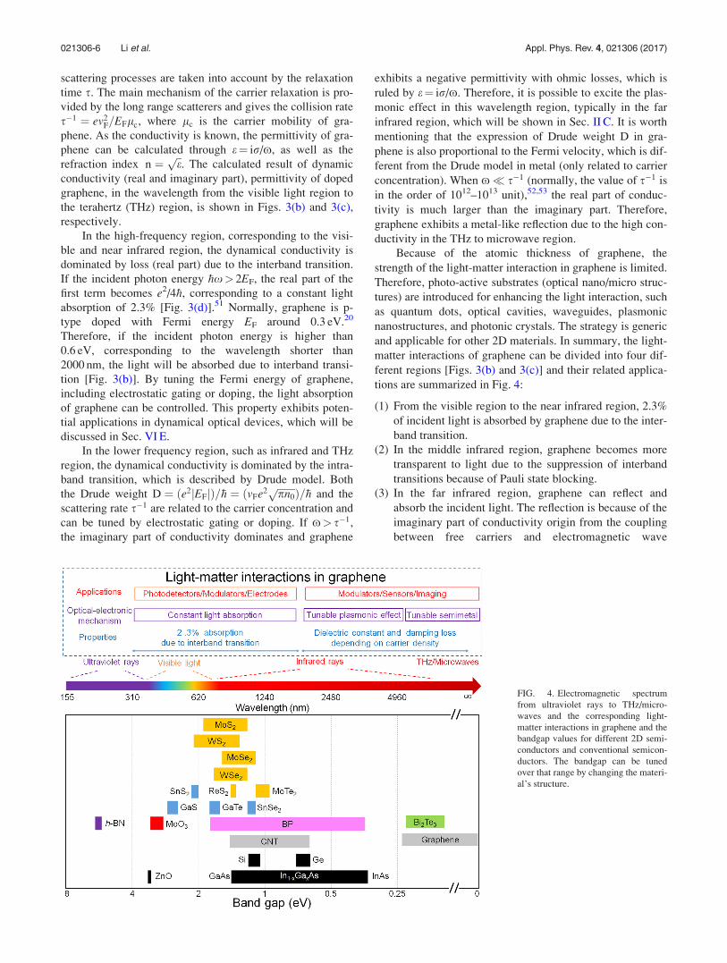
tions are summarized in Fig. 4:
(1) From the visible region to the near infrared region, 2.3%
of incident light is absorbed by graphene due to the inter-
band transition.
(2) In the middle infrared region, graphene becomes more
transparent to light due to the suppression of interband
transitions because of Pauli state blocking.
(3) In the far infrared region, graphene can reflect and
absorb the incident light. The reflection is because of the
imaginary part of conductivity origin from the coupling
between free carriers and electromagnetic wave
FIG. 4. Electromagnetic spectrum
from ultraviolet rays to THz/micro-
waves and the corresponding light-
matter interactions in graphene and the
bandgap values for different 2D semi-
conductors and conventional semicon-
ductors. The bandgap can be tuned
over that range by changing the materi-
al’s structure.
021306-6 Li et al. Appl. Phys. Rev. 4, 021306 (2017)

(EMW). The absorption is because of the ohmic loss of
free carriers.
(4) From the THz region to the microwave region, graphene
exhibits high reflection like metal because of the high
conductivity of graphene.
C. Graphene plasmons
Plasmons, the collective oscillations of free electrons
excited by EMW in noble metals, possess unique properties
for photonic technologies. Doped graphene emerges as an
alternative, unique 2D plasmonic material which displays a
wide range of extraordinary properties.54–59
Considering that a doped graphene is surrounded by
medias with dielectrics constants of e1 and e2 and the collec-
tive oscillations in graphene are excited by EMW of trans-
verse magnetic (TM) mode, the dispersion relation can be
simplified as50,54
Ksp ¼ e0
e1 þ e2
2
2ixr x; qð Þ
; (9)
where Ksp is a complex, where the real part represents the
propagating plasmonic wave, and the imaginary part repre-
sents the decay. The value of Ksp can be retraced to the
dynamical conductivity r(x) of graphene. The plasmonic
wave can be achieved in the far infrared region [Fig. 3(e)]57
as the significant imaginary conductivity and relatively small
Ohmic loss (real part) [Figs. 3(b) and 3(c)]. Graphene plas-
mons exhibit some unique properties due to the special
energy band structure of graphene: (1) Deep subwavelength
effect, which means that the plasmonic wavelength ksp in
graphene is extremely shorter than that in free space k0, as
shown in function ksp=k0 ¼ ð4a=ðe1 þ e2ÞÞðEF=�hxÞ, where a(�1/137) is the fine-structure constant. In the infrared fre-
quency, EF/�hx is on the order of 1, so the localized plas-
monic wavelength is two orders smaller than k0.55–57 (2)
Long distance in-plane propagation, which means that the
graphene plasmonic propagation distance (1=ðIm½Ksp�Þ) can
reach up to 100 plasmonic wavelengths.55,56 (3) High tun-
ability of the plamonic effect. As the dispersion relation is
dependent on the Fermi energy of graphene, the plasmons on
graphene can be controlled, e.g., by electrostatic gating, dop-
ing, and optical pumping.55–58
Localized plasmons in graphene nano/micro patterns
can be directly excited by EMW [Fig. 3(f)], which is another
kind of plasmonic mode paralleling to the propagating
surface plasmon.60–63 Without considering the interaction of
nearby patterns, the localized plasmon frequency for a nano-
pattern can be seen as a damped oscillator, and the effective
optical conductivity is given by the following functions:64
xpl ¼ffiffiffiffiffiffiffiffiffiffiffiffiffi
3D
8eem d
rand r xð Þ ¼ i
f D
px
x2 � x2p
� �þ iCx
; (10)
where d is the pattern size, em is the media dielectric con-
stant, e is the vacuum permittivity, C is the damping fre-
quency s�1, and f is the fill factor of the graphene area over
the total area. Drude weight is proportional to the Fermi
energy of graphene and thus the localized plasmon mode in
graphene can be controlled by electrostatic gating or doping.
D. 2D semiconductors
1. Electronic properties
Apart from semi-metallic graphene, 2D semiconductors
with finite bandgaps, such as TMDs, BP, and III–VI layered
materials, are particularly interesting for semiconductor
physics and devices.
The diversity and variability of band structures of 2D
TMDs which cover the range from semiconducting to metal-
lic make this kind of 2D materials a powerful candidate for
building functional devices. The band structures of 2D
TMDs differ a lot from their bulk crystals. As the material
becomes thinner from the bulk to the monolayer, the band
structure of TMDs transits from the smaller indirect bandgap
one to a larger direct bandgap one due to quantum confine-
ment effects.65,66 The lattice structure and band structure of
monolayer MoS2 are shown in Figs. 5(a) and 5(b), respec-
tively. Due to the heavy transition metal atoms and the
direct-gap band edges associated with d-orbital electrons,
TMDs have strong spin-orbit coupling (SOC), which greatly
differs from graphene.67,68 The spin degeneracy at the Kpoint in the valence band of monolayer TMD is removed by
SOC, while the degeneracy at the conduction band is con-
served [Fig. 5(b)].69 The energy splitting of the valence band
in monolayer MoS2 and MoSe2 is predicted to be 160 and
180 meV, respectively.67,70 Energy valley is another degree
of freedom in 2D TMDs beyond the spin. Two distinguished
valleys K and K0 points are presented at alternative corners
of the hexagonal Brillouin zone. The inverse symmetry
breaking leads to different orbital magnetic moments at Kand K0 points, making it possible to achieve valleytronic
devices [Fig. 5(c)]. Valley polarization in monolayer MoS2
can be approached by optical pumping with circularly polar-
ized light, and the consequent valley-based devices can be
fabricated.68,71 The valley degree of freedom can generate
an ultrahigh pseudo-magnetic field in monolayer TMDs and
lead to the valley quantum Hall effect.72,73
BP exhibits narrow bandgaps ranging from 0.3 eV (for
bulk) to 1.5 eV (for monolayer) depending on its thickness,
which bridges the spectral gap between zero-gap graphene
and relatively wide gap TMDs. Moreover, regardless of the
number of layers, BP shows an intrinsic direct-gap feature,
giving rise to potential applications in light detection and
emission in the infrared range.74 BP shows very strong in-
plane anisotropy with two nonequivalent lattice directions:
the zigzag one which is parallel to the phosphorus atomic
ridge and the armchair one which is perpendicular to the
ridge [Fig. 5(a)].75,76 This unusual anisotropy makes the
effective carrier mass of BP highly sensitive to the concerned
direction in the momentum space, as shown in Fig. 5(d).17
The consequent anisotropy electronic properties of BP are
investigated with the angular dependence of the conduc-
tance.75 Some other 2D semiconductors, such as ReS2, are
also reported to have similar anisotropy characteristics.77,78
A summary of band alignments of 2D semiconductors is
provided in Fig. 5(e).79 By choosing proper band alignment
021306-7 Li et al. Appl. Phys. Rev. 4, 021306 (2017)

(i.e., types I, II, and III) between 2D semiconductors, desired
applications could be achieved.
2. Optical properties
When illuminating a 2D semiconductor with photon
energy larger than its bandgap, the optical absorption occurs
exciting the electrons in the valence band into the conduction
band. The reverse process leads the electron and hole pairs
to relax to the band edges and then recombine as emitting
photons with energy equal to the bandgap of the semicon-
ductor, resulting in photoluminescence (PL). As shown in
Fig. 6(a), the electron and hole pair formed by a strong elec-
trostatic Coulomb force is regarded as an elementary excita-
tion called an exciton. The exciton is electrically neutral and
has an energy level within the bandgap of the semiconductor.
The binding energy of an exciton originating from the
Coulomb interaction would reduce the optical transition
energy but is negligible in bulk TMDs. However, the
Coulomb interaction is strongly increased when the TMD is
thinned down to the 2D system due to quantum confinement
effects.80 That is why in 2D TMD, the optical bandgap mea-
sured by optical methods is much smaller than the electronic
bandgap measured by electronic methods. For monolayer
MoS2, the exciton binding energy is in the range of 0.48 eV
to 0.89 eV,81,82 leading to the large difference between the
optical and electronic bandgaps. Therefore, it is a significant
issue about which kind of bandgap should be considered in
2D TMD devices.
For monolayer TMD semiconductors, two feature peaks
can be detected in PL and optical absorption (reflectance) spec-
tra, corresponding to A and B excitonic transitions associated
with the SOC-induced splitting of valence band edge [Fig.
6(b)].83 The peak positions of A and B excitons of monolayer
MoS2 are 1.8 and 2.0 eV, respectively.84 When increasing the
MoS2 film thickness, a slight red shift in both A and B exciton
peaks (�20 meV) is detected originating from the fact that the
direct bandgap of MoS2 is weakly dependent on the thick-
ness.84 For monolayer TMDs such as MoS2 and WS2, an
absorption rate for sunlight up to 5%–10% was reported,
which showed one order of magnitude higher than those in tra-
ditional semiconductors such as Si and GaAs.85 Furthermore,
electron-bound exciton, which is a negatively charged quasi-
particle consisting of two electrons and a hole, is usually called
a trion [Fig. 6(c)] and can be detected in PL and absorption
spectra of TMD semiconductors [Fig. 6(d)].86 Compared to the
bulk semiconductor, the binding energies of trions in mono-
layer TMDs are much larger (�18 meV for monolayer MoS2),
making the trion transition (A�) clearly observable.86 By
chemical doping and/or electrical gating on monolayer TMDs,
switching between exciton and trion peaks can be detected in
PL spectra.86,87 The exciton PL intensity of monolayer MoS2
can vary by two orders at different gating voltages, while the
FIG. 5. (a) Lattice structure of MoS2 and BP. (b) The band structure of monolayer MoS2 and the valence band edge and conduction band edge are indicated by
red and blue circles.69 Reprinted with permission from Yazyev et al., Mater. Today 18, 20 (2015). Copyright 2015 Elsevier Ltd. (c) Different orbital magnetic
moments at K and K0 points in MoS2, which correspond to the excitation/emission of left and right polarized light, respectively. (d) The anisotropic band struc-
ture of BP, the red and blue arrows present the effective mass for the different directions in the momentum space.17 Reprinted with permission from Phys.
Today 69(9), 38 (2016). Copyright 2016 AIP Publishing LLC. (e) Band alignments of 2D semiconductors relative to the vacuum level. The dotted lines indi-
cate the Hþ/H2, H2O/O2, and CO2 reduction potentials.79 Reprinted with permission from Peng et al., Nano Today 10, 128 (2015). Copyright 2015 Elsevier
Ltd.
021306-8 Li et al. Appl. Phys. Rev. 4, 021306 (2017)
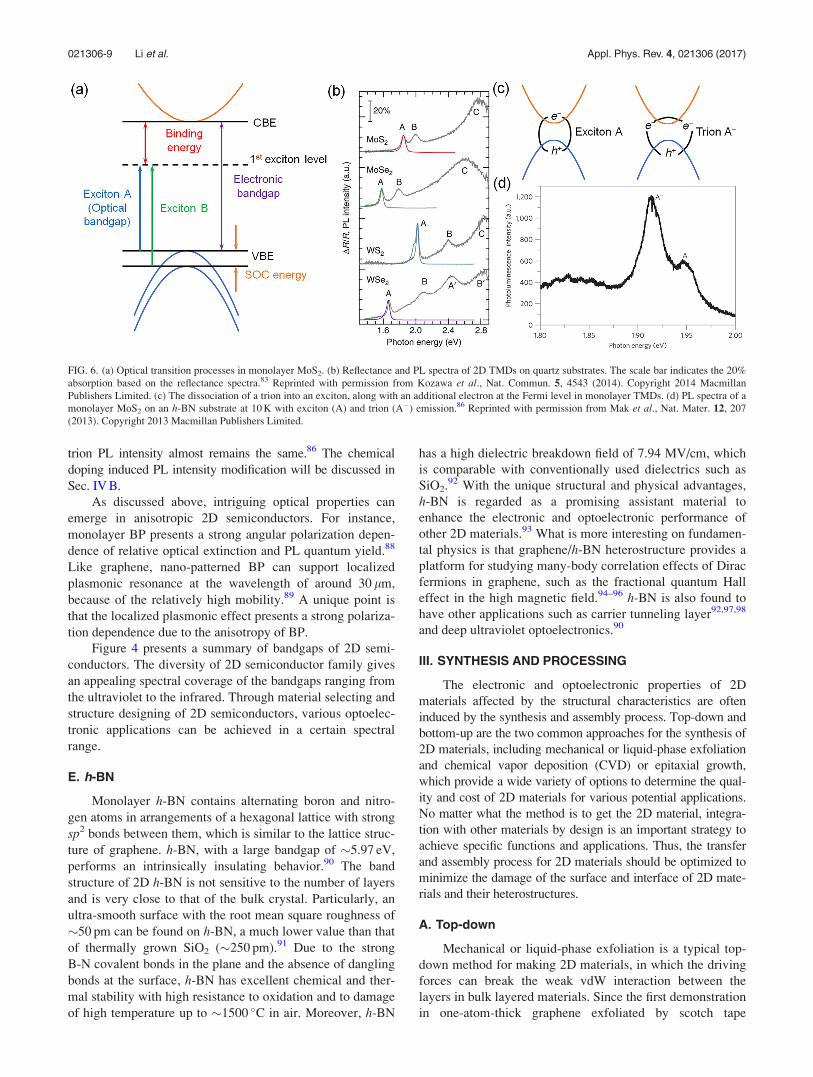
trion PL intensity almost remains the same.86 The chemical
doping induced PL intensity modification will be discussed in
Sec. IV B.
As discussed above, intriguing optical properties can
emerge in anisotropic 2D semiconductors. For instance,
monolayer BP presents a strong angular polarization depen-
dence of relative optical extinction and PL quantum yield.88
Like graphene, nano-patterned BP can support localized
plasmonic resonance at the wavelength of around 30 lm,
because of the relatively high mobility.89 A unique point is
that the localized plasmonic effect presents a strong polariza-
tion dependence due to the anisotropy of BP.
Figure 4 presents a summary of bandgaps of 2D semi-
conductors. The diversity of 2D semiconductor family gives
an appealing spectral coverage of the bandgaps ranging from
the ultraviolet to the infrared. Through material selecting and
structure designing of 2D semiconductors, various optoelec-
tronic applications can be achieved in a certain spectral
range.
E. h-BN
Monolayer h-BN contains alternating boron and nitro-
gen atoms in arrangements of a hexagonal lattice with strong
sp2 bonds between them, which is similar to the lattice struc-
ture of graphene. h-BN, with a large bandgap of �5.97 eV,
performs an intrinsically insulating behavior.90 The band
structure of 2D h-BN is not sensitive to the number of layers
and is very close to that of the bulk crystal. Particularly, an
ultra-smooth surface with the root mean square roughness of
�50 pm can be found on h-BN, a much lower value than that
of thermally grown SiO2 (�250 pm).91 Due to the strong
B-N covalent bonds in the plane and the absence of dangling
bonds at the surface, h-BN has excellent chemical and ther-
mal stability with high resistance to oxidation and to damage
of high temperature up to �1500 �C in air. Moreover, h-BN
has a high dielectric breakdown field of 7.94 MV/cm, which
is comparable with conventionally used dielectrics such as
SiO2.92 With the unique structural and physical advantages,
h-BN is regarded as a promising assistant material to
enhance the electronic and optoelectronic performance of
other 2D materials.93 What is more interesting on fundamen-
tal physics is that graphene/h-BN heterostructure provides a
platform for studying many-body correlation effects of Dirac
fermions in graphene, such as the fractional quantum Hall
effect in the high magnetic field.94–96 h-BN is also found to
have other applications such as carrier tunneling layer92,97,98
and deep ultraviolet optoelectronics.90
III. SYNTHESIS AND PROCESSING
The electronic and optoelectronic properties of 2D
materials affected by the structural characteristics are often
induced by the synthesis and assembly process. Top-down and
bottom-up are the two common approaches for the synthesis of
2D materials, including mechanical or liquid-phase exfoliation
and chemical vapor deposition (CVD) or epitaxial growth,
which provide a wide variety of options to determine the qual-
ity and cost of 2D materials for various potential applications.
No matter what the method is to get the 2D material, integra-
tion with other materials by design is an important strategy to
achieve specific functions and applications. Thus, the transfer
and assembly process for 2D materials should be optimized to
minimize the damage of the surface and interface of 2D mate-
rials and their heterostructures.
A. Top-down
Mechanical or liquid-phase exfoliation is a typical top-
down method for making 2D materials, in which the driving
forces can break the weak vdW interaction between the
layers in bulk layered materials. Since the first demonstration
in one-atom-thick graphene exfoliated by scotch tape
FIG. 6. (a) Optical transition processes in monolayer MoS2. (b) Reflectance and PL spectra of 2D TMDs on quartz substrates. The scale bar indicates the 20%
absorption based on the reflectance spectra.83 Reprinted with permission from Kozawa et al., Nat. Commun. 5, 4543 (2014). Copyright 2014 Macmillan
Publishers Limited. (c) The dissociation of a trion into an exciton, along with an additional electron at the Fermi level in monolayer TMDs. (d) PL spectra of a
monolayer MoS2 on an h-BN substrate at 10 K with exciton (A) and trion (A�) emission.86 Reprinted with permission from Mak et al., Nat. Mater. 12, 207
(2013). Copyright 2013 Macmillan Publishers Limited.
021306-9 Li et al. Appl. Phys. Rev. 4, 021306 (2017)

[Fig. 7(a)], this easy yet approachable exfoliation has been
serving as a promising processing method for proof-of-
concept demonstrations.1 The obtained 2D materials show
high-quality with few defects, which present remarkable fun-
damental electronic and optoelectronic properties. However,
this method is seriously restricted to wide applications due to
the low-throughput and difficulty of control. Liquid-phase
exfoliation is another top-down method which exfoliates the
layered crystals in solvents. In this process, matched solvents
(such as N-methyl-pyrrolidone and dimethylformamide) or
intercalators (such as butyllithium and metal naphthalenide)
are the key factors which could break the weak vdW interac-
tion between the layers via sonication [Fig. 7(b)].99–104
Particularly, the Hummers method has been used for synthe-
sis of large-scale graphene oxide (GO).105–108 The bulk
graphite is first oxidized to form graphite oxide, and then the
graphite oxide can be exfoliated into GO under sonication
and centrifugation. The reduced graphene oxide (rGO) could
be obtained by removal of oxygen-containing functional
groups. All these liquid-phase exfoliation methods for
preparing 2D materials are of low cost and provide high
yield. However, the crystal quality of 2D materials is often
degraded and many functional groups or residual solvent and
ions would affect the electrical properties of 2D materials.
B. Bottom-up
Due to the limitation of the top-down methods, bottom-
up approaches for the synthesis of 2D materials are espe-
cially important and urgent. Early research primarily focused
on the surface segregation of from the surface of transition
metals6 or epitaxial growth from the surface of silicon car-
bide.7 After that, CVD is a widely used method to synthesize
large-area and high-quality uniform 2D materials [Fig. 7(c)].
For the synthesis of graphene films, many metals, such as
Cu,109,110 Ni,111,112 Ge,113 and Pt114 have been used as the
growth substrates, where surface segregation/precipitation or
surface adsorption process of carbon was considered to be
the mechanism for graphene growth.115 Here, gas, liquid,
and solid carbon sources can be used for the synthesis of gra-
phene.116–119 In the case of hydrocarbon gas as a source, the
growth of graphene can be divided into the following steps:
(i) pyrolysis of hydrocarbon; (ii) adsorption, dehydrogena-
tion, and diffusion of carbon species on or into metal; and
(iii) nucleation and crystal growth. Thanks to the low carbon
solubility and easy processing technology, Cu is considered
to be a suitable choice for the growth of monolayer graphene
films.109 In this case, minimized carbon supply, high temper-
ature, and smooth Cu surface with minimal active sites will
result in a low nucleation density of graphene.120–122 Due to
the energetic favor of hydrogen–terminated graphene edges,
high H2 partial pressure can decrease the growth rate, while
oxygen, which is conducive to the dissociation of hydrocar-
bons, is found to increase the growth rate of graphene
domain.123–126 All these parameters will lead to the fast
growth of large single-crystal graphene.
Other 2D materials, such as h-BN,127–130 MoS2,131–135
WS2,136 MoSe2,137 WSe2,138 MoTe2,139 and ReS2140,141 are
also synthesized via bottom-up methods. Predeposition of a
metal layer on a substrate with a consequent chalcogenization
process can produce scalable 2D TMDs.142 Decomposition of
thiomolybdate is an alternative approach to obtain sizable 2D
TMDs.143 However, the above methods are likely to obtain
TMDs with nanoscale grain sizes. The most popular pro-
cesses for synthesizing high-quality and scalable 2D TMDs
are adopting metal oxide powders and chalcogen powders as
the precursors in CVD systems.131–134 It is found that the
growth of atomically thin TMDs can be promoted by adding
FIG. 7. (a) Mechanical exfoliation, (b) liquid-phase exfoliation, and (c) CVD approaches for the synthesis of 2D materials. (d) Wet transfer and (e) dry transfer
techniques for assembly of 2D materials.
021306-10 Li et al. Appl. Phys. Rev. 4, 021306 (2017)
seed molecules or creating step-edge structures on the sub-
strate due to the decreased nucleation energy barrier.133,144
The morphologies of 2D TMDs obtained by CVD methods
are highly dependent on the reaction temperature, the
amounts of precursors, and the precursor-substrate dis-
tance.145 Moreover, wafer-scale monolayer TMDs with high
spatial homogeneity are synthesized by the metal-organic
CVD technique.146
Furthermore, direct synthesis of vdWHs is of crucial
importance for electronic and optoelectronic applications.
Various kinds of vertical 2D heterostructures (e.g., graphene/
h-BN,147 MoS2-graphene148,149 and WSe2-MoS2150) are
achieved by sequential CVD growth and vdW epitaxy
method. Epitaxial 2D TMDs with controlled lattice orienta-
tion are obtained on nearly lattice matching substrates. On
the other side, lateral 2D heterostructures are also achieved
through strict control. Growing another 2D material on
patterned graphene can produce lateral junctions such as gra-
phene/h-BN151,152 and MoS2-graphene.153,154 Besides, 2D
TMD lateral heterostructures (e.g., WSe2-MoS2,) can be
grown by a two-step epitaxy growth strategy,155–159 in which
the formation of TMD alloys is suppressed due to different
growth temperatures and rates of each one.
C. Transfer and assembly
Device fabrication and heterostructure assembly based
on 2D materials require efficient and non-destructive transfer
methods. The polymer-protected wet transfer method has
been widely used for mechanical exfoliated or CVD-growth
2D materials.109,143,160 First, polymer such as poly(methyl-
methacrylate) (PMMA) is spin-coated onto the 2D material.
Second, the sample with the polymer coating layer is
detached from the substrate (e.g., etching Cu in a liquid etch-
ant or SiO2 in a NaOH/HF solution). At last, the polymer pro-
tected sample can be transferred to the target substrate and
the polymer is dissolved in an organic solvent [Fig. 7(d)].
Although the wet transfer method is easy in the process,
polymer residues can still be observed after dissolving and
they affect the electrical properties of 2D materials.37,161
Irregular wrinkles and cracks on the wet transferred 2D
materials are also hard to avoid, which have a negative effect
on electrical and optoelectronic performances of 2D materi-
als. Dry transfer methods have been developed to resolve the
above drawbacks of wet transfer processes.162–164 For exam-
ple, the poly(dimethylsiloxane) (PDMS) stamp first peels off
one 2D material from the substrate. When the PDMS stamp
with the 2D material is getting contact with another one,
both 2D layers are lifted up on the PDMS. By repeating this
procedure, more 2D layers can be added to achieve the 2D
material stacking with clean interfaces [Fig. 7(e)].
IV. STRUCTURAL MODIFICATIONS
This part will summarize the structural modifications of
2D materials, which could significantly adjust the physical
properties of these layered materials and affect the perfor-
mance of their electronic and optoelectronic devices. The
unique structural properties of 2D materials, such as defects,
dopants, component, phase, the number of layers, strain, and
corrugation at the nanoscale, which play a key role in proper-
ties, are emphatically surveyed.
A. Defects
Having defects in crystals is one of the most important
structural properties of semiconductors since it can alter their
electronic and optoelectronic properties. For instance,
defects can affect the local electronic structure, the carrier
density, the thermal conductivity, and the mechanical
strength of 2D materials. Point defects and line defects are
the most important lattice imperfections for 2D materials,
which are mainly generated at the synthesis process or/and
chemical/physical post-treatment.165,166 Moreover, the
defects in 2D materials could be observed or characterized
by High-resolution transmission electron microscopy
(HRTEM), scanning tunneling microscopy (STM), and
Raman spectroscopy, and theoretical calculations also pro-
vide the formation behavior of such structure.
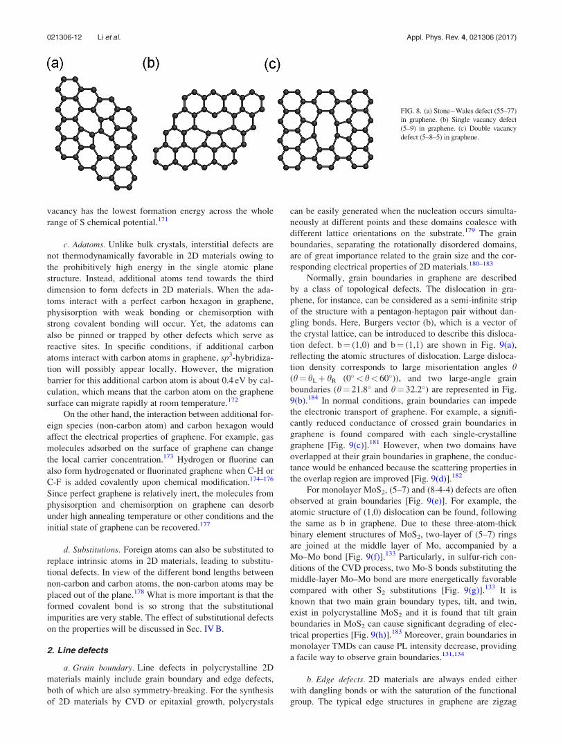
1. Point defects
a. Stone-Wales defect. Stone-Wales defect of graphene is
a unique defect containing two pentagons and two heptagons
(55–77) from rotating two p-bonded carbon atoms by 90�
[Fig. 8(a)].167 This reconstruction retains the pristine number
of atoms and does not involve any dangling bonds. Although
the formation energy of this Stone-Wales defect in graphene
is approximately 5 eV via calculation, the substantial energy
barrier is nearly 10 eV due to the rearrangements of carbon
atoms.167 This high energy means that the reconstruction is
stable at room temperature as long as the Stone-Wales defect
is formed.
b. Vacancy defects. Vacancy defects are the lattice sites
where one or more atoms are missing. When an odd number
of carbon atoms are missing in graphene, dangling bonds
will remain due to geometrical reasons which make the
structure chemically active and many functional groups,
such as hydroxyl and carboxyl can be easily attached to the
vacancy defects. For instance, single vacancy in graphene
results in the formation of a (5–9) defect [Fig. 8(b)].168 In
particular, the formation energy for the single vacancy is as
high as 7.4 eV in graphene, while its migration energy is
about 1.7 eV by calculation.169 On the other hand, when an
even number of carbon atoms are missing, the dangling
bonds can be healed for the connectivity of carbon atoms.
For a double vacancy in graphene, no dangling bond is pre-
sent and a reconstructed (5-8-5) defect is thermodynamically
favored [Fig. 8(c)].170 Meanwhile, the migration for the dou-
ble vacancy is about 7 eV, higher than the energy for the sin-
gle vacancy, making this double vacancy immobile.169
In contrast to the one-atom-thick graphene, the vacancy
defects in 2D TMDs are far more complex because of the
three-atom-thick binary element structures of monolayer
TMDs. In monolayer MoS2, different types of defects are
involved, including mono- and disulfur vacancies, vacancy
complex of Mo and nearby three sulfur, and vacancy com-
plex of Mo and nearby three di-sulfur pairs. Density func-
tional theory (DFT) calculations show that the mono-sulfur
021306-11 Li et al. Appl. Phys. Rev. 4, 021306 (2017)
vacancy has the lowest formation energy across the whole
range of S chemical potential.171
c. Adatoms. Unlike bulk crystals, interstitial defects are
not thermodynamically favorable in 2D materials owing to
the prohibitively high energy in the single atomic plane
structure. Instead, additional atoms tend towards the third
dimension to form defects in 2D materials. When the ada-
toms interact with a perfect carbon hexagon in graphene,
physisorption with weak bonding or chemisorption with
strong covalent bonding will occur. Yet, the adatoms can
also be pinned or trapped by other defects which serve as
reactive sites. In specific conditions, if additional carbon
atoms interact with carbon atoms in graphene, sp3-hybridiza-
tion will possibly appear locally. However, the migration
barrier for this additional carbon atom is about 0.4 eV by cal-
culation, which means that the carbon atom on the graphene
surface can migrate rapidly at room temperature.172
On the other hand, the interaction between additional for-
eign species (non-carbon atom) and carbon hexagon would
affect the electrical properties of graphene. For example, gas
molecules adsorbed on the surface of graphene can change
the local carrier concentration.173 Hydrogen or fluorine can
also form hydrogenated or fluorinated graphene when C-H or
C-F is added covalently upon chemical modification.174–176
Since perfect graphene is relatively inert, the molecules from
physisorption and chemisorption on graphene can desorb
under high annealing temperature or other conditions and the
initial state of graphene can be recovered.177
d. Substitutions. Foreign atoms can also be substituted to
replace intrinsic atoms in 2D materials, leading to substitu-
tional defects. In view of the different bond lengths between
non-carbon and carbon atoms, the non-carbon atoms may be
placed out of the plane.178 What is more important is that the
formed covalent bond is so strong that the substitutional
impurities are very stable. The effect of substitutional defects
on the properties will be discussed in Sec. IV B.
2. Line defects
a. Grain boundary. Line defects in polycrystalline 2D
materials mainly include grain boundary and edge defects,
both of which are also symmetry-breaking. For the synthesis
of 2D materials by CVD or epitaxial growth, polycrystals
can be easily generated when the nucleation occurs simulta-
neously at different points and these domains coalesce with
different lattice orientations on the substrate.179 The grain
boundaries, separating the rotationally disordered domains,
are of great importance related to the grain size and the cor-
responding electrical properties of 2D materials.180–183
Normally, grain boundaries in graphene are described
by a class of topological defects. The dislocation in gra-
phene, for instance, can be considered as a semi-infinite strip
of the structure with a pentagon-heptagon pair without dan-
gling bonds. Here, Burgers vector (b), which is a vector of
the crystal lattice, can be introduced to describe this disloca-
tion defect. b¼ (1,0) and b¼ (1,1) are shown in Fig. 9(a),
reflecting the atomic structures of dislocation. Large disloca-
tion density corresponds to large misorientation angles h(h¼ hLþ hR (0�< h< 60�)), and two large-angle grain
boundaries (h¼ 21.8� and h¼ 32.2�) are represented in Fig.
9(b).184 In normal conditions, grain boundaries can impede
the electronic transport of graphene. For example, a signifi-
cantly reduced conductance of crossed grain boundaries in
graphene is found compared with each single-crystalline
graphene [Fig. 9(c)].181 However, when two domains have
overlapped at their grain boundaries in graphene, the conduc-
tance would be enhanced because the scattering properties in
the overlap region are improved [Fig. 9(d)].182
For monolayer MoS2, (5–7) and (8-4-4) defects are often
observed at grain boundaries [Fig. 9(e)]. For example, the
atomic structure of (1,0) dislocation can be found, following
the same as b in graphene. Due to these three-atom-thick
binary element structures of MoS2, two-layer of (5–7) rings
are joined at the middle layer of Mo, accompanied by a
Mo–Mo bond [Fig. 9(f)].133 Particularly, in sulfur-rich con-
ditions of the CVD process, two Mo-S bonds substituting the
middle-layer Mo–Mo bond are more energetically favorable
compared with other S2 substitutions [Fig. 9(g)].133 It is
known that two main grain boundary types, tilt, and twin,
exist in polycrystalline MoS2 and it is found that tilt grain
boundaries in MoS2 can cause significant degrading of elec-
trical properties [Fig. 9(h)].183 Moreover, grain boundaries in
monolayer TMDs can cause PL intensity decrease, providing
a facile way to observe grain boundaries.131,134
b. Edge defects. 2D materials are always ended either
with dangling bonds or with the saturation of the functional
group. The typical edge structures in graphene are zigzag
FIG. 8. (a) Stone�Wales defect (55–77)
in graphene. (b) Single vacancy defect
(5–9) in graphene. (c) Double vacancy
defect (5–8–5) in graphene.
021306-12 Li et al. Appl. Phys. Rev. 4, 021306 (2017)

and armchair edges [Fig. 9(i)], which exhibit the minimized
number of dangling bonds. Significantly, the bandgap of gra-
phene nanoribbon with narrow widths (<10 nm) and well-
defined edge structures can be tuned, which makes it possible
to be used in high-performance electronic devices. In the
structure of CVD-grown monolayer MoS2, single-crystal tri-
angles with well-defined edges orient either along Mo-
zigzag or along S-zigzag directions [Fig. 9(j)]. For the case
of narrow ribbons, particularly, edges can serve as the scat-
tering centers for electrons and phonons.
B. Dopants
Dopants are desirable because these foreign species can
adjust the Fermi level, modify the electronic structure, or
inject charge into the electron system of 2D materials.
Spatially controlled doping by ion implantation has been
widely used in bulk semiconductors. However, alternative
methods for doping 2D materials have to be investigated,
since the ion implantation technique is difficult to be adopted
in the 2D system. Substitutions and adatoms in 2D materials
are the important categories besides electrostatic doping.
1. Substitutional doping
Substitutional doping of foreign atoms offers a control-
lable and stable doping method for 2D materials. Typically,
boron (B, called an acceptor), the substitutional impurity
atom replacing a carbon atom, can dope graphene as p-type
(hole is created in the valence band). Similarly, nitrogen (N)
atoms (called a donor) can dope graphene to n-type (the elec-
tron is donated to the lattice in the conduction band). These
substitutional dopants may lead to strong scattering by which
the electrical conduction of graphene is greatly affected. For
example, n-type graphene can be achieved by introducing N-
contained precursors, such as NH3, CH3CN, and C5H5N,
accompanied by the carbon source in the CVD growth pro-
cess [Fig. 10(a)].185–188 Besides, post-growth treatments,
such as plasma treatment in N-contained gas, are also imple-
mented to dope graphene.189,190 It is found that the N-doped
graphene exhibits a lower carrier mobility but larger on/off
ratio than that of intrinsic graphene.186 Although the carrier-
defect scattering can affect the carrier mobility, the substitu-
tional N atoms can alter the electronic structure of graphene
and make it meaningful in electronic and optoelectronic
devices. In addition to B and N,191 other substitutional
atoms, such as phosphorus (P),192 silicon (Si),193 and sulfur
(S),194 can also dope graphene. Besides, some substitutional
doping methods both during synthesis and post treatment are
adopted in 2D semiconductors.195–198 For instance, manga-
nese (Mn) doped MoS2 via in situ vapor phase deposition on
graphene would modify its band structure, and the substrate
surface chemistry is the dominant factor in this doping
FIG. 9. (a) Dislocations with Burgers vector (1,0) and (1,1) in graphene. (b) Atomic structures of large-angle grain boundaries.184 (a) and (b) Reprinted with
permission from Yazyev et al., Phys. Rev. B 81, 195420 (2010). Copyright 2010 American Physical Society. (c) Current–voltage curves measured across the
grain boundary of graphene (green) and within the each graphene grain (red and blue). The inset is the image of this device.181 Reprinted with permission from
Yu et al., Nat. Mater. 10, 443 (2011). Copyright 2011 Macmillan Publishers Limited. (d) Gate-voltage dependent conductance measured across an overlapped
grain boundary of graphene (L–R) and within the each graphene grain (L and R). The inset is the image of this device with the 325 nm width of the overlap
region.182 Reprinted with permission from Tsen et al., Science 336, 1143 (2012). Copyright 2012 AAAS. (e) Scanning transmission electron microscopy
(annular dark field) images of a MoS2 grain boundary and schematics of the Mo-oriented (5–7) dislocation (f) and its S2 substitutions (g). The purple sphere is
Mo, and the yellow and orange ones represent top and bottom S, respectively.133 Reprinted with permission from Najmaei et al., Nat. Mater. 12, 754 (2013).
Copyright 2013 Macmillan Publishers Limited. (h) Electrical transport transfer curves for the pristine MoS2 device and two devices with two types of grain
boundaries (twin and tilt boundaries).183 Reprinted with permission from Najmaei et al., ACS Nano 8, 7930 (2014). Copyright 2014 American Chemical
Society. (i) The zigzag and the armchair edges in graphene. (j) The single-crystal triangles with well-defined edges orient either along Mo-zigzag or along S-
zigzag directions in MoS2.
021306-13 Li et al. Appl. Phys. Rev. 4, 021306 (2017)
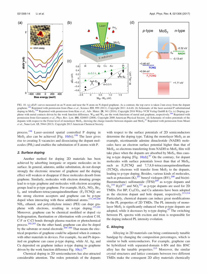
process.198 Laser–assisted spatial controlled P doping in
MoS2 also can be achieved [Fig. 10(b)].198 The laser gives
rise to creating S vacancies and dissociating the dopant mol-
ecules (PH3) and enables the substitution of S atoms with P.
2. Surface doping
Another method for doping 2D materials has been
achieved by adsorbing inorganic or organic molecules on its
surface. In general, adatoms, unlike substitution, do not disrupt
strongly the electronic structure of graphene and the doping
effect will weaken or disappear if these molecules desorb from
graphene. Similarly, molecules with electron donating groups
lead to n-type graphene and molecules with electron accepting
groups lead to p-type graphene. For example, H2O2, NO2, Br2,
I2, and tetrafluoro-tetracyanoquinodimethane (F4-TCNQ) are
the strong electron acceptors and graphene can be p-type
doped when interacting with these additional atoms.173,199,200
NH3, ethanol, and poly(ethylene imine) (PEI) can dope gra-
phene with electrons, resulting in n-type doping.173,201
Moreover, graphene can be chemical modified or doped viahydrogenation, fluorination or chlorination with covalent C-H,
C-F or C-Cl bonds through plasma reaction or photochemical
process.202,203 On the other hand, graphene can also be doped
by the substrate or metal electrode.204–206 That means the elec-
trical properties of graphene could be adjusted when it contacts
with other materials in devices. For example, Au and Pt depos-
ited on graphene can cause p-type doping, while Al, Ag, and
Cu deposited on graphene induce n-type doping to graphene
driven by the work function difference Fig. 10(c).206
Chemical doping in 2D semiconductors has also attracted
considerable attention. The redox potentials of the dopants
with respect to the surface potentials of 2D semiconductors
determine the doping type. Taking the monolayer MoS2 as an
example, nicotinamide adenine dinucleotide (NADH) mole-
cules have an electron surface potential higher than that of
MoS2, so electrons transferring from NADH to MoS2 film will
take place when the dopants are absorbed by MoS2, thus caus-
ing n-type doping [Fig. 10(d)].87 On the contrary, for dopant
molecules with surface potentials lower than that of MoS2,
such as F4TCNQ and 7,7,8,8-tetracyanoquinodimethane
(TCNQ), electrons will transfer from MoS2 to the dopants,
leading to p-type doping. Besides, various kinds of molecules,
such as potassium (K),207 benzyl viologen (BV),208 and bis(tri-
fluoromethane) sulfonamide (TFSI)209 as n-type dopants and
O2,210 H2O211 and NO2212 as p-type dopants are used for 2D
TMDs. For BP, Cs2CO3, and Cu adatoms have been adopted
as the electron dopant and hole dopant, respectively.213,214
Particularly, chemical dopants can induce great modifications
to the PL properties of 2D TMDs. The PL intensity of mono-
layer MoS2 is significantly enhanced when p-type dopants are
adopted, while it decreases by n-type doping.87 The switching
between PL spectra with exciton and trion is responsible for
the doping induced PL intensity evolution.
C. Alloying
Alloying in 2D materials can bring continuously tunable
bandgap by changing the composition percentages, which is
similar to bulk semiconductors. For example, graphene can
be hybridized with separated-domain h-BN and this BNC
alloy has the tunable properties.215 Moreover, the similar
crystal structures and lattice constants between two different
TMDs make the consequent 2D alloy materials chemically
FIG. 10. (a) dI/dV curves measured on an N atom and near the N atom on N-doped graphene. As a contrast, the top curve is taken 2 nm away from the dopant
graphene.185 Reprinted with permission from Zhao et al., Science 333, 999 (2011). Copyright 2011 AAAS. (b) Schematic of the laser-assisted P substitutional
doping in MoS2.198 Reprinted with permission from Kim et al., Adv. Mater. 28, 341 (2016). Copyright 2016 Wiley-VCH Verlag GmbH & Co. (c) Doping gra-
phene with metal contacts driven by the work function difference. WM and WG are the work functions of metal and graphene, respectively.206 Reprinted with
permission from Giovannetti et al., Phys. Rev. Lett. 101, 026803 (2008). Copyright 2008 American Physical Society. (d) Schematic of redox potentials of the
dopants with respect to the Fermi level of monolayer MoS2, showing the charge transfer between dopants and MoS2.87 Reprinted with permission from Mouri
et al., Nano Lett. 13, 5944 (2013). Copyright 2013 American Chemical Society.
021306-14 Li et al. Appl. Phys. Rev. 4, 021306 (2017)
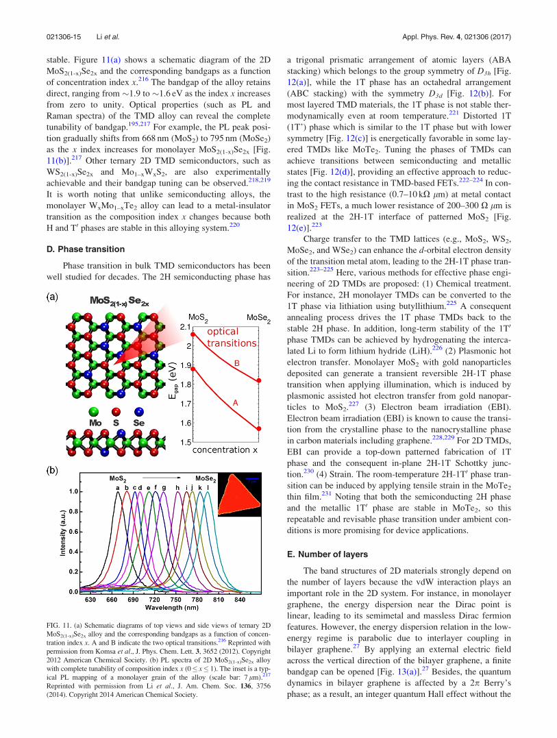
stable. Figure 11(a) shows a schematic diagram of the 2D
MoS2(1-x)Se2x and the corresponding bandgaps as a function
of concentration index x.216 The bandgap of the alloy retains
direct, ranging from �1.9 to �1.6 eV as the index x increases
from zero to unity. Optical properties (such as PL and
Raman spectra) of the TMD alloy can reveal the complete
tunability of bandgap.195,217 For example, the PL peak posi-
tion gradually shifts from 668 nm (MoS2) to 795 nm (MoSe2)
as the x index increases for monolayer MoS2(1-x)Se2x [Fig.
11(b)].217 Other ternary 2D TMD semiconductors, such as
WS2(1-x)Se2x and Mo1–xWxS2, are also experimentally
achievable and their bandgap tuning can be observed.218,219
It is worth noting that unlike semiconducting alloys, the
monolayer WxMo1–xTe2 alloy can lead to a metal-insulator
transition as the composition index x changes because both
H and T0 phases are stable in this alloying system.220
D. Phase transition
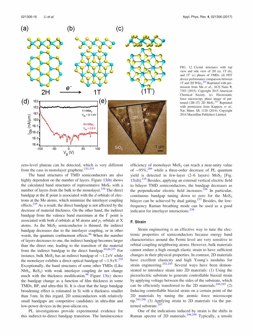
Phase transition in bulk TMD semiconductors has been
well studied for decades. The 2H semiconducting phase has
a trigonal prismatic arrangement of atomic layers (ABA
stacking) which belongs to the group symmetry of D3h [Fig.
12(a)], while the 1T phase has an octahedral arrangement
(ABC stacking) with the symmetry D3d [Fig. 12(b)]. For
most layered TMD materials, the 1T phase is not stable ther-
modynamically even at room temperature.221 Distorted 1T
(1T’) phase which is similar to the 1T phase but with lower
symmetry [Fig. 12(c)] is energetically favorable in some lay-
ered TMDs like MoTe2. Tuning the phases of TMDs can
achieve transitions between semiconducting and metallic
states [Fig. 12(d)], providing an effective approach to reduc-
ing the contact resistance in TMD-based FETs.222–224 In con-
trast to the high resistance (0.7–10 kX lm) at metal contact
in MoS2 FETs, a much lower resistance of 200–300 X lm is
realized at the 2H-1T interface of patterned MoS2 [Fig.
12(e)].223
Charge transfer to the TMD lattices (e.g., MoS2, WS2,
MoSe2, and WSe2) can enhance the d-orbital electron density
of the transition metal atom, leading to the 2H-1T phase tran-
sition.223–225 Here, various methods for effective phase engi-
neering of 2D TMDs are proposed: (1) Chemical treatment.
For instance, 2H monolayer TMDs can be converted to the
1T phase via lithiation using butyllithium.225 A consequent
annealing process drives the 1T phase TMDs back to the
stable 2H phase. In addition, long-term stability of the 1T0
phase TMDs can be achieved by hydrogenating the interca-
lated Li to form lithium hydride (LiH).226 (2) Plasmonic hot
electron transfer. Monolayer MoS2 with gold nanoparticles
deposited can generate a transient reversible 2H-1T phase
transition when applying illumination, which is induced by
plasmonic assisted hot electron transfer from gold nanopar-
ticles to MoS2.227 (3) Electron beam irradiation (EBI).
Electron beam irradiation (EBI) is known to cause the transi-
tion from the crystalline phase to the nanocrystalline phase
in carbon materials including graphene.228,229 For 2D TMDs,
EBI can provide a top-down patterned fabrication of 1T
phase and the consequent in-plane 2H-1T Schottky junc-
tion.230 (4) Strain. The room-temperature 2H-1T0 phase tran-
sition can be induced by applying tensile strain in the MoTe2
thin film.231 Noting that both the semiconducting 2H phase
and the metallic 1T0 phase are stable in MoTe2, so this
repeatable and revisable phase transition under ambient con-
ditions is more promising for device applications.
E. Number of layers
The band structures of 2D materials strongly depend on
the number of layers because the vdW interaction plays an
important role in the 2D system. For instance, in monolayer
graphene, the energy dispersion near the Dirac point is
linear, leading to its semimetal and massless Dirac fermion
features. However, the energy dispersion relation in the low-
energy regime is parabolic due to interlayer coupling in
bilayer graphene.27 By applying an external electric field
across the vertical direction of the bilayer graphene, a finite
bandgap can be opened [Fig. 13(a)].27 Besides, the quantum
dynamics in bilayer graphene is affected by a 2p Berry’s
phase; as a result, an integer quantum Hall effect without the
FIG. 11. (a) Schematic diagrams of top views and side views of ternary 2D
MoS2(1-x)Se2x alloy and the corresponding bandgaps as a function of concen-
tration index x. A and B indicate the two optical transitions.216 Reprinted with
permission from Komsa et al., J. Phys. Chem. Lett. 3, 3652 (2012). Copyright
2012 American Chemical Society. (b) PL spectra of 2D MoS2(1-x)Se2x alloy
with complete tunability of composition index x (0 x 1). The inset is a typ-
ical PL mapping of a monolayer grain of the alloy (scale bar: 7 lm).217
Reprinted with permission from Li et al., J. Am. Chem. Soc. 136, 3756
(2014). Copyright 2014 American Chemical Society.
021306-15 Li et al. Appl. Phys. Rev. 4, 021306 (2017)
zero-level plateau can be detected, which is very different
from the case in monolayer graphene.232,233
The band structures of TMD semiconductors are also
highly dependent on the number of layers. Figure 13(b) shows
the calculated band structures of representative MoS2 with a
number of layers from the bulk to the monolayer.234 The direct
bandgap at the K point is associated with the d orbitals of elec-
trons at the Mo atoms, which minimize the interlayer coupling
effects.235 As a result, the direct bandgap is not affected by the
decrease of material thickness. On the other hand, the indirect
bandgap from the valence band maximum at the C point is
associated with both d orbitals at M atoms and pz orbitals at X
atoms. As the MoS2 semiconductor is thinned, the indirect
bandgap decreases due to the interlayer coupling, or in other
words, the quantum confinement effects.66 When the number
of layers decreases to one, the indirect bandgap becomes larger
than the direct one, leading to the transition of the material
from the indirect bandgap to the direct bandgap.65,66,235 For
instance, bulk MoS2 has an indirect bandgap of �1.2 eV while
the monolayer exhibits a direct optical bandgap of �1.9 eV.235
Exceptionally, the band structures of some other TMDs (Like
NbS2, ReS2) with weak interlayer coupling do not change
much with the thickness modification.66 Figure 13(c) shows
the bandgap change as a function of film thickness in some
TMDs, BP, and ultra-thin Si. It is clear that the large bandgap
broadening effect is estimated in Si with a thickness smaller
than 3 nm. In this regard, 2D semiconductors with relatively
small bandgaps are competitive candidates in ultra-thin and
low-power devices in the post-silicon era.
PL investigations provide experimental evidence for
this indirect-to-direct bandgap transition. The luminescence
efficiency of monolayer MoS2 can reach a near-unity value
of �95%,209 while a three-order decrease of PL quantum
yield is detected in few-layer (2–6 layers) MoS2 [Fig.
13(d)].235 Besides, applying an external vertical electric field
to bilayer TMD semiconductors, the bandgap decreases as
the perpendicular electric field increases.236 In particular,
continuous bandgap tuning down to zero for the MoS2
bilayer can be achieved by dual gating.237 Besides, the low-
frequency Raman breathing mode can be used as a good
indicator for interlayer interactions.238
F. Strain
Strain engineering is an effective way to tune the elec-
tronic properties of semiconductors because energy band
characteristics around the Fermi level are very sensitive to
orbital coupling neighboring atoms. However, bulk materials
cannot endure a high enough elastic strain to have sufficient
changes in their physical properties. In contrast, 2D materials
have excellent elasticity and high Young’s modulus for
strain engineering.242,243 Several ways have been demon-
strated to introduce strain into 2D materials: (1) Using the
piezoelectric substrate to generate controllable biaxial strain
by applying voltage between the sides of the substrate, which
can be efficiently transferred to the 2D materials.244,245 (2)
Inducing controllable biaxial strain on a certain point of the
2D materials by tuning the atomic force microscope
tip.243,246 (3) Applying strain to 2D materials via the pat-
terned substrate.247
One of the indications induced by strain is the shifts in
Raman spectra of 2D materials.248,249 Typically, a tensile
FIG. 12. Crystal structures with top
view and side view of 2H (a), 1T (b),
and 1T0 (c) phases of TMDs. (d) FET
device performance comparison between
1T and 2H WSe2.224 Reprinted with per-
mission from Ma et al., ACS Nano 9,
7383 (2015). Copyright 2015 American
Chemical Society. (e). Electrostatic
force microscopy phase image of pat-
terned (2H-1T) 2D MoS2.223 Reprinted
with permission from Kappera et al.,Nat. Mater. 13, 1128 (2014). Copyright
2014 Macmillan Publishers Limited.
021306-16 Li et al. Appl. Phys. Rev. 4, 021306 (2017)

strain induces redshifts while the compressive strain induces
blue shifts in Raman in-plane vibrational modes. It has
shown that under uniaxial tensile strain, the Raman G peak
of graphene gives a redshift at a rate of @xG=@eh
¼ �14:2 cm�1=%, where xG is the frequency of the G mode
and eh is the hydrostatic component of strain;29 and that
under biaxial compressive strain, the Raman G peak gives a
blue shift at a rate of @xG=@ell ¼ �57:3 cm�1=%, where ell
indicates the parallel strain tensor component.244 Unlike the
biaxial strain, the uniaxial strain is anisotropical, thus break-
ing the hexagonal symmetry in 2D materials. As a result,
some Raman modes associated with high symmetry of 2D
materials will be split under large uniaxial strain [Fig.
14(a)].249 In contrast, when biaxial strain is applied in mono-
layer MoS2, the E2g mode remains symmetrical.245
Strain engineering offers an efficient and controllable
way to open graphene’s bandgap. The first-principles calcu-
lation has predicted that 1% uniaxial strain could create a
300 meV bandgap opening in graphene [Fig. 14(b)].29
Patterned substrate induced periodical strain in graphene
could result in bandgap opening.247 Strain-induced bandgap
engineering of 2D semiconductors is another interesting
topic. Theoretical works have shown that compressive strain
makes the bandgap increase while tensile strain makes
the bandgap decrease in 2D TMD semiconductors.250
Furthermore, the direct to indirect bandgap transition in 2D
TMDs would occur when strain is applied [Fig. 14(c)].65 The
biaxial compressive strain could make a 100 meV per % PL
blueshift in monolayer MoS2,245 while uniaxial tensile strain
could induce PL red shifts in monolayer MoS2 [Fig.
FIG. 13. (a) Schematic diagrams of lattice structures and the corresponding band structures of monolayer graphene, bilayer graphene, and bilayer graphene
under the vertical electrical field. The opened bandgap 2D can be tuned by the magnitude of the field.27 Reprinted with permission from Oostinga et al., Nat.
Mater. 7, 151 (2008). Copyright 2008 Macmillan Publishers Limited. (b) Band structures of MoS2 from the bulk to the monolayer (1L). The arrows show the
transitions from valence band edge to the conduction band edge with the lowest energy.234 Reprinted with permission from Splendiani et al., Nano Lett. 10,
1271 (2010). Copyright 2010 American Chemical Society. (c) Bandgap as a function of film thickness in TMDs, BP, and ultra-thin Si.235,239–241 (d) PL spectra
of monolayer and bilayer MoS2, while the inset shows PL quantum yield of MoS2 (1L-6L).235 Reprinted with permission from Mak et al., Phys. Rev. Lett.
105, 136805 (2010). Copyright 2010 American Physical Society.
FIG. 14. (a) Raman G band of monolayer graphene as a function of applied uniaxial strain. G band splitting into Gþ and G� modes occurs at large strain, indi-
cating the strain-induced symmetry breaking in graphene.249 Reprinted with permission from Mohiuddin et al., Phys. Rev. B 79, 205433 (2009). Copyright
2009 American Physical Society. (b) Schematic of uniaxial tensile stress applied in graphene and the calculated band structure of 1% tensile strained graphene.
An opened bandgap can be clearly observed.29 Reprinted with permission from Ni et al., ACS Nano 2, 2301 (2008). Copyright 2008 American Chemical
Society. (c) Bandgap of monolayer MoS2 as a function of applied strain. The direct bandgap of pristine MoS2 becomes indirect and even metallic when tensile
strain is applied.65 Reprinted with permission from Yun et al., Phys. Rev. B 85, 033305 (2012). Copyright 2012 American Physical Society. (d) PL spectra of
monolayer MoS2 (Inset, Scalar bar, 6 lm) under various magnitudes of tensile strain.251 Reprinted with permission from Liu et al., Nat. Commun. 5, 5246
(2014). Copyright 2014 Macmillan Publishers Limited.
021306-17 Li et al. Appl. Phys. Rev. 4, 021306 (2017)
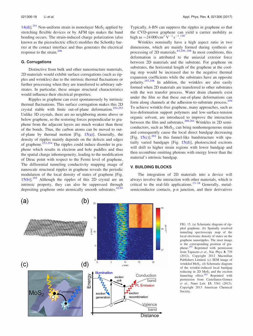
14(d)].251 Non-uniform strain in monolayer MoS2 applied by
stretching flexible devices or by AFM tips makes the band
bending occurs. The strain-induced charge polarization (also
known as the piezoelectric effect) modifies the Schottky bar-
rier at the contact interface and thus generates the electrical
response to the strain.246
G. Corrugations
Distinctive from bulk and other nanostructure materials,
2D materials would exhibit surface corrugations (such as rip-
ples and wrinkles) due to the intrinsic thermal fluctuations or
further processing when they are transferred to arbitrary sub-
strates. In particular, these unique structural characteristics
would influence their electrical properties.
Ripples in graphene can exist spontaneously by intrinsic
thermal fluctuations. This surface corrugation makes this 2D
crystal stable with finite out-of-plane deformation.252,253
Unlike 3D crystals, there are no neighboring atoms above or
below graphene, so the restoring forces perpendicular to gra-
phene from the adjacent layers are much weaker than those
of the bonds. Thus, the carbon atoms can be moved to out-
of-plane by thermal motion [Fig. 15(a)]. Generally, the
density of ripples mainly depends on the defects and edges
of graphene.253,254 The ripples could induce disorder in gra-
phene which results in electron and hole puddles and thus
the spatial charge inhomogeneity, leading to the modification
of Dirac point with respect to the Fermi level of graphene.
The differential tunneling conductivity mapping image of
nanoscale structural ripples in graphene reveals the periodic
modulation of the local density of states of graphene [Fig.
15(b)].255 Although the ripples of this 2D crystal are an
intrinsic property, they can also be suppressed through
depositing graphene onto atomically smooth substrates.42,93
Typically, h-BN can suppress the ripples in graphene so that
the CVD-grown graphene can yield a carrier mobility as
high as �24 000 cm2 V�1 s�1.130
Wrinkles nominally have a high aspect ratio in two
dimensions, which are mainly formed during synthesis or
processing of 2D materials.43,256–258 In most conditions, this
deformation is attributed to the uniaxial exterior force
between 2D materials and the substrate. For graphene on
substrates, the horizontal length of the graphene at the cool-
ing step would be increased due to the negative thermal
expansion coefficients while the substrates have an opposite
polarity.257,258 In addition, the wrinkles are also easily
formed when 2D materials are transferred to other substrates
with the wet transfer process. Water drain channels exist
under the film so that these out-of-plane deformations can
form along channels at the adhesion-to-substrate process.259
To achieve wrinkle-free graphene, many approaches, such as
less-deformation support polymers and low-surface-tension
organic solvent, are introduced to improve the interaction
between the film and substrates.260,261 Wrinkles in 2D semi-
conductors, such as MoS2, can bring nonhomogeneous strain
and consequently cause the local direct bandgap decreasing
[Fig. 15(c)].262 In this funnel-like bandstructure with spa-
tially varied bandgaps [Fig. 15(d)], photoexcited excitons
will drift to higher strain regions with lower bandgap and
then recombine emitting photons with energy lower than the
material’s intrinsic bandgap.
V. BUILDING BLOCKS
The integration of 2D materials into a device will
always involve the interaction with other materials, which is
critical to the real-life applications.13–18 Generally, metal-
semiconductor contacts, p-n junction, and their derivatives
FIG. 15. (a) Schematic diagram of rip-
pled graphene. (b) Spatially resolved
tunneling spectroscopy map of the
local electronic density of states on the
graphene nanoripples. The inset image
is the corresponding position of gra-
phene.255 Reprinted with permission
from Tapaszto et al., Nat. Phys. 8, 739
(2012). Copyright 2012 Macmillan
Publishers Limited. (c) SEM image of
wrinkled MoS2. (d) Schematic diagram
of the wrinkle-induced local bandgap
reducing in 2D MoS2 and the exciton
funneling effect.262 Reprinted with
permission from Castellanos-Gomez
et al., Nano Lett. 13, 5361 (2013).
Copyright 2013 American Chemical
Society.
021306-18 Li et al. Appl. Phys. Rev. 4, 021306 (2017)
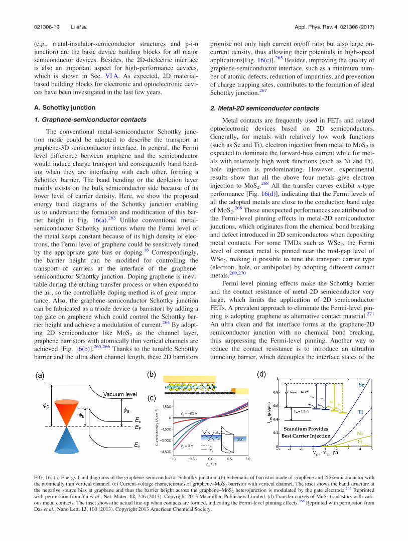
(e.g., metal-insulator-semiconductor structures and p-i-n
junction) are the basic device building blocks for all major
semiconductor devices. Besides, the 2D-dielectric interface
is also an important aspect for high-performance devices,
which is shown in Sec. VI A. As expected, 2D material-
based building blocks for electronic and optoelectronic devi-
ces have been investigated in the last few years.
A. Schottky junction
1. Graphene-semiconductor contacts
The conventional metal-semiconductor Schottky junc-
tion mode could be adopted to describe the transport at
graphene-3D semiconductor interface. In general, the Fermi
level difference between graphene and the semiconductor
would induce charge transport and consequently band bend-
ing when they are interfacing with each other, forming a
Schottky barrier. The band bending or the depletion layer
mainly exists on the bulk semiconductor side because of its
lower level of carrier density. Here, we show the proposed
energy band diagrams of the Schottky junction enabling
us to understand the formation and modification of this bar-
rier height in Fig. 16(a).263 Unlike conventional metal-
semiconductor Schottky junctions where the Fermi level of
the metal keeps constant because of its high density of elec-
trons, the Fermi level of graphene could be sensitively tuned
by the appropriate gate bias or doping.18 Correspondingly,
the barrier height can be modified for controlling the
transport of carriers at the interface of the graphene-
semiconductor Schottky junction. Doping graphene is inevi-
table during the etching transfer process or when exposed to
the air, so the controllable doping method is of great impor-
tance. Also, the graphene-semiconductor Schottky junction
can be fabricated as a triode device (a barristor) by adding a
top gate on graphene which could control the Schottky bar-
rier height and achieve a modulation of current.264 By adopt-
ing 2D semiconductor like MoS2 as the channel layer,
graphene barristors with atomically thin vertical channels are
achieved [Fig. 16(b)].265,266 Thanks to the tunable Schottky
barrier and the ultra short channel length, these 2D barristors
promise not only high current on/off ratio but also large on-
current density, thus allowing their potentials in high-speed
applications[Fig. 16(c)].265 Besides, improving the quality of
graphene-semiconductor interface, such as a minimum num-
ber of atomic defects, reduction of impurities, and prevention
of charge trapping sites, contributes to the formation of ideal
Schottky junction.267
2. Metal-2D semiconductor contacts
Metal contacts are frequently used in FETs and related
optoelectronic devices based on 2D semiconductors.
Generally, for metals with relatively low work functions
(such as Sc and Ti), electron injection from metal to MoS2 is
expected to dominate the forward-bias current while for met-
als with relatively high work functions (such as Ni and Pt),
hole injection is predominating. However, experimental
results show that all the above four metals give electron
injection to MoS2.268 All the transfer curves exhibit n-type
performance [Fig. 16(d)], indicating that the Fermi levels of
all the adopted metals are close to the conduction band edge
of MoS2.268 These unexpected performances are attributed to
the Fermi-level pinning effects in metal-2D semiconductor
junctions, which originates from the chemical bond breaking
and defect introduced in 2D semiconductors when depositing
metal contacts. For some TMDs such as WSe2, the Fermi
level of contact metal is pinned near the mid-gap level of
WSe2, making it possible to tune the transport carrier type
(electron, hole, or ambipolar) by adopting different contact
metals.269,270
Fermi-level pinning effects make the Schottky barrier
and the contact resistance of metal-2D semiconductor very
large, which limits the application of 2D semiconductor
FETs. A prevalent approach to eliminate the Fermi-level pin-
ning is adopting graphene as alternative contact material.271
An ultra clean and flat interface forms at the graphene-2D
semiconductor junction with no chemical bond breaking,
thus suppressing the Fermi-level pinning. Another way to
reduce the contact resistance is to introduce an ultrathin
tunneling barrier, which decouples the interface states of the
FIG. 16. (a) Energy band diagrams of the graphene-semiconductor Schottky junction. (b) Schematic of barristor made of graphene and 2D semiconductor with
the atomically thin vertical channel. (c) Current-voltage characteristics of graphene–MoS2 barristor with vertical channel. The inset shows the band structure at
the negative source bias at graphene and thus the barrier height across the graphene–MoS2 heterojunction is modulated by the gate electrode.265 Reprinted
with permission from Yu et al., Nat. Mater. 12, 246 (2013). Copyright 2013 Macmillan Publishers Limited. (d) Transfer curves of MoS2 transistors with vari-
ous metal contacts. The inset shows the actual line-up when contacts are formed, indicating the Fermi-level pinning effects.268 Reprinted with permission from
Das et al., Nano Lett. 13, 100 (2013). Copyright 2013 American Chemical Society.
021306-19 Li et al. Appl. Phys. Rev. 4, 021306 (2017)
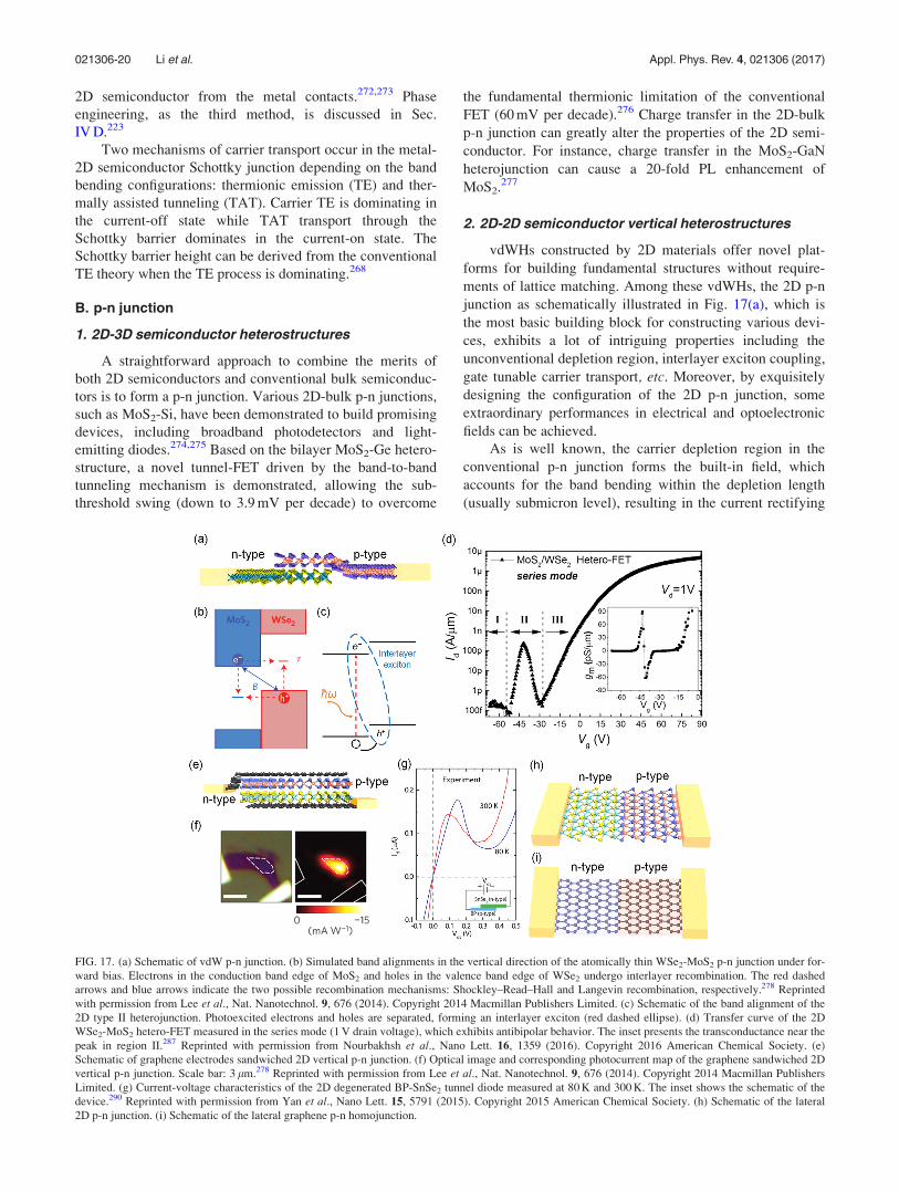
2D semiconductor from the metal contacts.272,273 Phase
engineering, as the third method, is discussed in Sec.
IV D.223
Two mechanisms of carrier transport occur in the metal-
2D semiconductor Schottky junction depending on the band
bending configurations: thermionic emission (TE) and ther-
mally assisted tunneling (TAT). Carrier TE is dominating in
the current-off state while TAT transport through the
Schottky barrier dominates in the current-on state. The
Schottky barrier height can be derived from the conventional
TE theory when the TE process is dominating.268
B. p-n junction
1. 2D-3D semiconductor heterostructures
A straightforward approach to combine the merits of
both 2D semiconductors and conventional bulk semiconduc-
tors is to form a p-n junction. Various 2D-bulk p-n junctions,
such as MoS2-Si, have been demonstrated to build promising
devices, including broadband photodetectors and light-
emitting diodes.274,275 Based on the bilayer MoS2-Ge hetero-
structure, a novel tunnel-FET driven by the band-to-band
tunneling mechanism is demonstrated, allowing the sub-
threshold swing (down to 3.9 mV per decade) to overcome
the fundamental thermionic limitation of the conventional
FET (60 mV per decade).276 Charge transfer in the 2D-bulk
p-n junction can greatly alter the properties of the 2D semi-
conductor. For instance, charge transfer in the MoS2-GaN
heterojunction can cause a 20-fold PL enhancement of
MoS2.277
2. 2D-2D semiconductor vertical heterostructures
vdWHs constructed by 2D materials offer novel plat-
forms for building fundamental structures without require-
ments of lattice matching. Among these vdWHs, the 2D p-n
junction as schematically illustrated in Fig. 17(a), which is
the most basic building block for constructing various devi-
ces, exhibits a lot of intriguing properties including the
unconventional depletion region, interlayer exciton coupling,
gate tunable carrier transport, etc. Moreover, by exquisitely
designing the configuration of the 2D p-n junction, some
extraordinary performances in electrical and optoelectronic
fields can be achieved.
As is well known, the carrier depletion region in the
conventional p-n junction forms the built-in field, which
accounts for the band bending within the depletion length
(usually submicron level), resulting in the current rectifying
FIG. 17. (a) Schematic of vdW p-n junction. (b) Simulated band alignments in the vertical direction of the atomically thin WSe2-MoS2 p-n junction under for-
ward bias. Electrons in the conduction band edge of MoS2 and holes in the valence band edge of WSe2 undergo interlayer recombination. The red dashed
arrows and blue arrows indicate the two possible recombination mechanisms: Shockley–Read–Hall and Langevin recombination, respectively.278 Reprinted
with permission from Lee et al., Nat. Nanotechnol. 9, 676 (2014). Copyright 2014 Macmillan Publishers Limited. (c) Schematic of the band alignment of the
2D type II heterojunction. Photoexcited electrons and holes are separated, forming an interlayer exciton (red dashed ellipse). (d) Transfer curve of the 2D
WSe2-MoS2 hetero-FET measured in the series mode (1 V drain voltage), which exhibits antibipolar behavior. The inset presents the transconductance near the
peak in region II.287 Reprinted with permission from Nourbakhsh et al., Nano Lett. 16, 1359 (2016). Copyright 2016 American Chemical Society. (e)
Schematic of graphene electrodes sandwiched 2D vertical p-n junction. (f) Optical image and corresponding photocurrent map of the graphene sandwiched 2D
vertical p-n junction. Scale bar: 3 lm.278 Reprinted with permission from Lee et al., Nat. Nanotechnol. 9, 676 (2014). Copyright 2014 Macmillan Publishers
Limited. (g) Current-voltage characteristics of the 2D degenerated BP-SnSe2 tunnel diode measured at 80 K and 300 K. The inset shows the schematic of the
device.290 Reprinted with permission from Yan et al., Nano Lett. 15, 5791 (2015). Copyright 2015 American Chemical Society. (h) Schematic of the lateral
2D p-n junction. (i) Schematic of the lateral graphene p-n homojunction.
021306-20 Li et al. Appl. Phys. Rev. 4, 021306 (2017)
behavior of the p-n junction. However, the 2D vdW p-n junc-
tion, in which both the vertical p- and n-channels are atomi-
cally thin, could have completely distinguished carrier
transport mechanisms from those in the bulk p-n junction.
Figure 17(b) illustrates the band diagrams of the WSe2-MoS2
p-n junction under forward bias in the vertical direction.
Within each semiconductor lateral transport channel, no
appreciable potential barriers can be detected [Fig. 17(b)].278
The lack of the depletion region in the 2D vdW p-n junction
makes the forward bias current to be governed by interlayer
carrier recombination instead of band bending modification.
Two physical mechanisms may be attributed to the interlayer
recombination between electrons in the conduction band
of MoS2 and holes in the valence band of WSe2:
Shockley–Read–Hall recombination assisted by carrier
tunneling into trap states and Langevin recombination asso-
ciated with the interlayer exciton.278 At a reverse bias, how-
ever, depletion of holes in WSe2 and electrons in MoS2
occurs in the junction area, causing the large band bending
between overlapping (junction) and non-overlapping (homo-
geneous material) regions in the lateral direction.278
Theoretical calculations have predicted the type-II band
alignment of various 2D vdWHs, such as WS2-MoS2, WS2-
MoSe2, and WSe2-MoSe2 vdWHs.279–281 This facilitates the
exciton dissociation in the 2D vdW p-n junction, which is
essential in optoelectronic applications such as photodetec-
tion and light harvesting. Experimental results have shown
ultrafast carrier transfer in the 2D p-n junction (hole transfer
rate �50 fs in the WS2-MoS2 junction).282 After the photo-
excited electrons and holes relaxed to the conduction band
edge of the n-type TMD and the valence band edge of the
p-type TMD, interlayer excitons are formed by the Coulomb
interaction (interlayer coupling), as shown in Fig.
17(c).283,284 The novel interlayer exciton in the 2D p-n junc-
tion can be clearly detected by PL spectroscopy.284,285 The
lifetime of an interlayer exciton can be much longer than
that of an intralayer exciton, resulting from the spatially
indirect nature and the lowest energy configuration of the
interlayer exciton. Moreover, electrical gating can modify
the band alignment of the 2D p-n junction and thus tune the
interlayer exciton resonance.284 On the other hand, light
absorption associated with the interlayer transition is
observed in 2D vdW p-n junctions, while the photon energy
is much lower than the intrinsic bandgap of each individual
material.286 These strong interlayer coupling effects in atom-
ically thin p-n junction originate from the 2D nature and the
lack of depletion region in vdWHs, which differs a lot from
the case of the conventional bulk p-n junction.
The atomically thin nature of the 2D vdW p-n junction
enables the electrostatically tunable carrier transport behav-
ior. The gate-dependent transport of the 2D vdWHs results
from the integrated effects of transfer characteristics of indi-
vidual p- and n-channels. As is shown in Fig. 17(d), the
transfer curve of the hetero-FET on the 2D WSe2-MoS2 p-n
junction has three distinct regions.287 Large series resistance
occurs at the junction when either of the 2D semiconductors
is depleted, resulting in the low drain current even the other
2D semiconductor is carrier conducting. The intriguing anti-
bipolar behavior of the p-n junction is exclusive to the 2D
system with tunable carrier concentration, providing a
unique platform for circuit and optoelectronic applications,
for instance, wavelength-selective light detection by electri-
cal gating.288
Both the overlapping junction region and the non-
overlapping individual 2D material region of the 2D vdW
p-n junction contribute to its carrier transport. Taking 2D
MoTe2-MoS2 junction as an example, it is found that the
device properties, such as drain current, are strongly depen-
dent on the device configuration (short or long non-
overlapping region).289 In fact, the non-overlapping channel
with high resistance causes the relatively low on-current den-
sity and low electrical/photonic response speed in the stack-
ing 2D p-n diode, which limits its potential in practical
applications. One solution is to apply transparent graphene
as electrodes on the all-overlapping vertical stacking 2D p-n
junction [Fig. 17(e)].278 This device configuration enables an
atomically thin semiconducting channel, giving rise to the
large on-current density and efficient photoexcited carrier
separation in the junction region [Fig. 17(f)).
The tunnel diode (Esaki diode) can be fabricated on 2D
vdWHs using highly doped 2D materials or dual-gated con-
figuration to achieve the broken-gap band alignment.290,291
For example, prominent negative differential resistance
(NDR) behavior was observed in the degenerate 2D BP-
SnSe2 p-n junction even at room temperature [Fig. 17(g)].290
Carrier band-to-band tunneling dominates the forward-bias
transport in the NDR region. 2D tunnel diodes pave the way
for potential applications such as tunnel-FET for low-power
electronics, oscillator circuit, and multi-valued logics.
3. 2D-2D semiconductor lateral heterostructures
Apart from the widely studied 2D vertical vdWHs, 2D
lateral heterostructures [Fig. 17(h)] have gained increasing
attention because of the atomically sharp interface with
covalent bonds and the easier band offset tuning in the lateral
junction.155–159,292 The in-plane junction configuration
results in carrier transporting through the lateral direction
without interlayer transport. In this regard, the 2D lateral p-n
heterojunction has band bending and finite depletion region,
which is similar to the bulk p-n junction. Using scanning
Kelvin probe force microscopy, researchers are able to deter-
mine the built-in field profile and the depletion length in the
2D lateral heterojunction.155,159
4. Homostructures
As the ion injection technique at present is not available
for 2D materials, alternative methods, such as dual gating
configuration, selective chemical doping, and layer engineer-
ing, are applied to fabricate the lateral p-n homostructure in
2D materials (such as MoS2, MoSe2, and WSe2) for optoelec-
tronics.293–295 On the other hand, the graphene p-n homojunc-
tion [Fig. 17(i)] shows some distinguished electronic
properties due to its special carrier behaviors. The current
rectifying effect cannot be observed because the electrons in
graphene are ruled by the Klein tunneling effect.32 However,
open circuit voltage and photocurrent at the graphene p-n
homojunction mainly come from the photo-thermoelectric
021306-21 Li et al. Appl. Phys. Rev. 4, 021306 (2017)
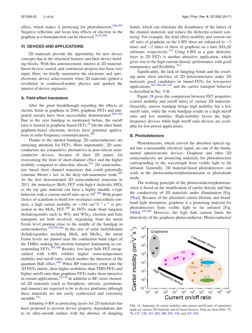
effect, which makes it promising for photodetectors.296,297
Negative reflection and focus lens effects of electron in the
graphene p-n homojunction can be observed.34,35,298
VI. DEVICES AND APPLICATIONS
2D materials provide the opportunity for new device
concepts due to the structural features and their device build-
ing blocks. With this announcement, interest in 2D material-
based devices soared, and continuous progress has been very
rapid. Here, we briefly summarize the electronic and opto-
electronic device achievements when 2D materials ignited a
revolution in condensed-matter physics and sparked the
interest of device engineers.
A. Field effect transistors
After the great breakthrough regarding the effects of
electric fields in graphene in 2004, graphene FETs and inte-
grated circuits have been successfully demonstrated.299–301
Due to the zero bandgap as mentioned before, the on/off
ratio is limited in graphene-based FETs.24 On the other hand,
graphene-based electronic devices have potential applica-
tions in radio frequency communications.302
Thanks to the opened bandgap, 2D semiconductors are
attracting attention for FETs. More importantly, 2D semi-
conductors are competitive alternatives in post-silicon semi-
conductor devices, because of their 2D nature for
overcoming the limit of short-channel effect and the higher
mobility compared to ultra-thin silicon.241 2D semiconduc-
tors based short channel transistors that could potentially
continue Moore’s law in the deep sub-nanometer node.303
As the first demonstrated 2D semiconductor transistor in
2011, the monolayer MoS2 FET with high-k dielectric HfO2
as the top gate material can have a highly tunable n-type
behavior with a current on/off ratio up to 108.304 With proper
choice of scandium to build low-resistance source/drain con-
tacts, a high carrier mobility of �184 cm2 V�1 s�1 is pre-
sented in the MoS2 FET.268 In FETs made from tungsten
dichalcogenides such as WS2 and WSe2, electron and hole
transports are both involved, originating from the metal
Fermi level pinning close to the middle of the bandgap in
semiconductors.270,305,306 In the case of some molybdenum
dichalcogenides including MoS2 and MoSe2, the metal
Fermi levels are pinned near the conduction band edges of
the TMDs, making the electron transport dominating in cor-
responding FETs.307,308 Besides, few-layer InSe FET encap-
sulated with h-BN exhibits higher room-temperature
mobility and on/off ratio, which enables the detection of the
quantum Hall effect.309 When BP transistors come into the
2D FETs family, their higher mobilities than TMD FETs and
higher on/off ratio than graphene FETs make them attractive
in certain applications.76,310 In addition to BP, more elemen-
tal 2D materials (such as borophene, silicene, germanene,
and stanene) are expected to be in device platforms although
these materials are not easily synthesized and extremely
unstable.311
Adopting h-BN as protecting layers for 2D materials has
been proposed to prevent device property degradations due
to its ultra-smooth surface with the absence of dangling
bonds, which can eliminate the disturbance of the lattice of
the channel materials and reduce the dielectric-related scat-
tering. For example, the field effect mobility and current on/
off ratio of graphene on the h-BN sheet are enhanced to �3
times and �2 times of those of graphene on a bare SiO2/Si
substrate, respectively.312 Using h-BN as a gate dielectric
layer in 2D FETs is another attractive application, which
gives rise to the high-current-density performance with good
transparency and flexibility.313
Significantly, the lack of dangling bonds and the result-
ing more ideal interface of 2D heterostructures make 2D
materials good candidates in tunnel-FETs for low-power
applications,287,290,291,314 and the carrier transport behavior
is described in Sec. V B.
Figure 18 gives the comparison between FET properties
(carrier mobility and on/off ratio) of various 2D materials.
Generally, narrow bandgap brings high mobility but a low
on/off ratio, while the wide bandgap results in a high on/off
ratio and low mobility. High-mobility favors the high-
frequency devices while high on/off ratio devices are avail-
able for low-power applications.
B. Photodetectors
Photodetectors, which convert the absorbed optical sig-
nal into a measurable electrical signal, are one of the funda-
mental optoelectronic devices. Graphene and other 2D
semiconductors are promising materials for photodetectors
corresponding to the wavelength from visible light to far
infrared. Generally, 2D material-based photodetectors can
work in the photoconductor/phototransistor or photodiode
mode.
The working principle of the photoconductor/phototran-
sistor is based on the modification of carrier density and thus
the conductivity of 2D materials under illumination [Fig.
19(a)]. Because of the ultrashort carrier lifetime and broad-
band light absorption, graphene is a promising material for
photodetectors from visible light to far infrared [Fig.
19(b)].319,320 However, the high dark current limits the
detectivity of the graphene photoconductor. Photoconductor/
FIG. 18. Summary of carrier mobility and current on/off ratio of transistors
made on various 2D materials and Si-based devices. Data are from Refs. 75,
76, 137, 138, 143, 269, 300, 301, 310, and 315–318.
021306-22 Li et al. Appl. Phys. Rev. 4, 021306 (2017)
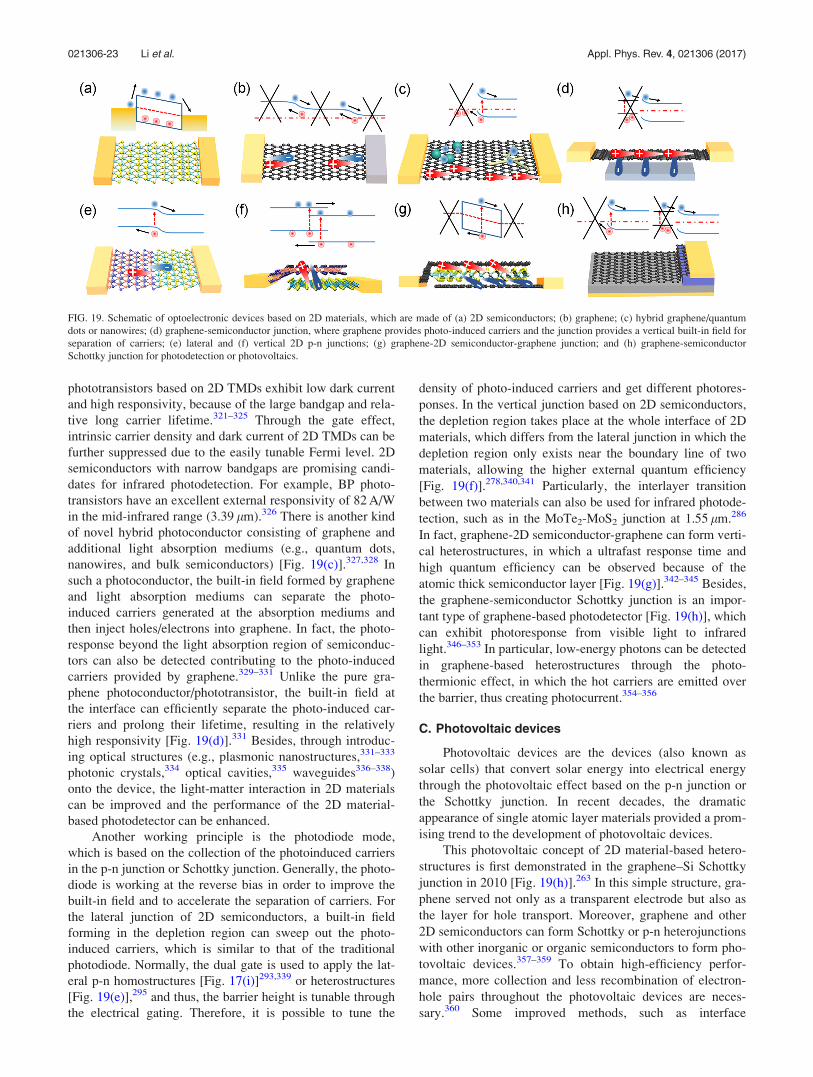
phototransistors based on 2D TMDs exhibit low dark current
and high responsivity, because of the large bandgap and rela-
tive long carrier lifetime.321–325 Through the gate effect,
intrinsic carrier density and dark current of 2D TMDs can be
further suppressed due to the easily tunable Fermi level. 2D
semiconductors with narrow bandgaps are promising candi-
dates for infrared photodetection. For example, BP photo-
transistors have an excellent external responsivity of 82 A/W
in the mid-infrared range (3.39 lm).326 There is another kind
of novel hybrid photoconductor consisting of graphene and
additional light absorption mediums (e.g., quantum dots,
nanowires, and bulk semiconductors) [Fig. 19(c)].327,328 In
such a photoconductor, the built-in field formed by graphene
and light absorption mediums can separate the photo-
induced carriers generated at the absorption mediums and
then inject holes/electrons into graphene. In fact, the photo-
response beyond the light absorption region of semiconduc-
tors can also be detected contributing to the photo-induced
carriers provided by graphene.329–331 Unlike the pure gra-
phene photoconductor/phototransistor, the built-in field at
the interface can efficiently separate the photo-induced car-
riers and prolong their lifetime, resulting in the relatively
high responsivity [Fig. 19(d)].331 Besides, through introduc-
ing optical structures (e.g., plasmonic nanostructures,331–333
photonic crystals,334 optical cavities,335 waveguides336–338)
onto the device, the light-matter interaction in 2D materials
can be improved and the performance of the 2D material-
based photodetector can be enhanced.
Another working principle is the photodiode mode,
which is based on the collection of the photoinduced carriers
in the p-n junction or Schottky junction. Generally, the photo-
diode is working at the reverse bias in order to improve the
built-in field and to accelerate the separation of carriers. For
the lateral junction of 2D semiconductors, a built-in field
forming in the depletion region can sweep out the photo-
induced carriers, which is similar to that of the traditional
photodiode. Normally, the dual gate is used to apply the lat-
eral p-n homostructures [Fig. 17(i)]293,339 or heterostructures
[Fig. 19(e)],295 and thus, the barrier height is tunable through
the electrical gating. Therefore, it is possible to tune the
density of photo-induced carriers and get different photores-
ponses. In the vertical junction based on 2D semiconductors,
the depletion region takes place at the whole interface of 2D
materials, which differs from the lateral junction in which the
depletion region only exists near the boundary line of two
materials, allowing the higher external quantum efficiency
[Fig. 19(f)].278,340,341 Particularly, the interlayer transition
between two materials can also be used for infrared photode-
tection, such as in the MoTe2-MoS2 junction at 1.55 lm.286
In fact, graphene-2D semiconductor-graphene can form verti-
cal heterostructures, in which a ultrafast response time and
high quantum efficiency can be observed because of the
atomic thick semiconductor layer [Fig. 19(g)].342–345 Besides,
the graphene-semiconductor Schottky junction is an impor-
tant type of graphene-based photodetector [Fig. 19(h)], which
can exhibit photoresponse from visible light to infrared
light.346–353 In particular, low-energy photons can be detected
in graphene-based heterostructures through the photo-
thermionic effect, in which the hot carriers are emitted over
the barrier, thus creating photocurrent.354–356
C. Photovoltaic devices
Photovoltaic devices are the devices (also known as
solar cells) that convert solar energy into electrical energy
through the photovoltaic effect based on the p-n junction or
the Schottky junction. In recent decades, the dramatic
appearance of single atomic layer materials provided a prom-
ising trend to the development of photovoltaic devices.
This photovoltaic concept of 2D material-based hetero-
structures is first demonstrated in the graphene–Si Schottky
junction in 2010 [Fig. 19(h)].263 In this simple structure, gra-
phene served not only as a transparent electrode but also as
the layer for hole transport. Moreover, graphene and other
2D semiconductors can form Schottky or p-n heterojunctions
with other inorganic or organic semiconductors to form pho-
tovoltaic devices.357–359 To obtain high-efficiency perfor-
mance, more collection and less recombination of electron-
hole pairs throughout the photovoltaic devices are neces-
sary.360 Some improved methods, such as interface
FIG. 19. Schematic of optoelectronic devices based on 2D materials, which are made of (a) 2D semiconductors; (b) graphene; (c) hybrid graphene/quantum
dots or nanowires; (d) graphene-semiconductor junction, where graphene provides photo-induced carriers and the junction provides a vertical built-in field for
separation of carriers; (e) lateral and (f) vertical 2D p-n junctions; (g) graphene-2D semiconductor-graphene junction; and (h) graphene-semiconductor
Schottky junction for photodetection or photovoltaics.
021306-23 Li et al. Appl. Phys. Rev. 4, 021306 (2017)

improvement,361 material doping,362–366 and optical struc-
ture design,361,367 are applied to the much more efficient and
stable photovoltaic devices, and the power conversion effi-
ciency has exceeded 15%.361 Furthermore, in the atomically
sharp 2D vdW p-n junctions (such as MoS2–WSe2), efficient
photoinduced carriers can be separated and high external
quantum efficiencies can be achieved [Fig. 19(f)].85,368 A
unique feature of these vdW photovoltaic devices is the tun-
able majority carrier density by the gate voltage. In
particular, the sandwich structure with 2D semiconductors
for the light absorber between graphene (such as gra-
phene-TMDs-graphene) can achieve efficient photoinduced
carrier separation when the work function of graphene is
modified by gate voltage or doping methods [Fig.
19(g)].342–344 In the future, various other configured
designs and optoelectronic effects of 2D material-based
heterostructures, for instance, multiple junctions, localized
surface plasmons, thermophotovoltaic effect, and hot car-
rier concept, are urgently needed for enhancing the power
conversion efficiency.
D. Light emission devices
The unique band structures of monolayer TMD semi-
conductors with direct bandgaps of visible to NIR ranges
make them promising candidates for light generation.
Electroluminescence (EL) is realized in the monolayer MoS2
FET, which arises from the same excited state (exciton
A).369 It is found that the EL emission is localized at the
metal contacts, which can be attributed to the maximized
exciton generation efficiency through impact excitation at
carrier injection areas. Hence, the homogeneous 2D material
device is not likely suitable for practical light emission appli-
cation since the quantum efficiency is limited (�10�5 for
monolayer MoS2).370 An effective solution is to build a p-n
junction (light emission diode, LED) for light generation
(Fig. 20). The lateral p-n junction in monolayer TMDs by
the dual-gating strategy is first achieved for light emission in
2014.293,370,371 Apart from the lateral LED where the active
region is still localized by the depletion region, vertical
vdWHs are also raised up for efficient carrier injection in
LED with its large active region at the whole overlapping
area.278,340 In order to reduce the leakage current in the verti-
cal stacking structures, functional stacking structures for
light emission are developed by inserting tunneling layers
(e.g., h-BN and Al2O3) into the p-n junction and/or the elec-
trode contacts, which enables the long lifetime of excitons in
TMD quantum wells.372,373 With this band-structure engi-
neering strategy, the EL quantum efficiency of 10% could be
achieved in monolayer TMDs, which is comparable to those
of organic LEDs.372
Quantum emitters (made of quantum confined structures
such as quantum dots and defects) can generate single pho-
tons, which is crucial for applications such as quantum infor-
mation and high-resolution metrology. TMD quantum
emitters with a very sharp photon emission spectrum are fab-
ricated.374–376 Furthermore, laser, which generates coherent
light source, has been implemented in the 2D system.
Monolayer WSe2 as the gain medium coupling to an exqui-
sitely designed photonic crystal cavity structure shows an
ultralow optical pumping threshold (27 nW at 130 K).377
E. Electro-optic modulators
The optical modulator is used for tuning the properties
(e.g., intensity and phase) of the incident EMW. Graphene
is a promising material for the modulator device due to its
tunable dielectric constant.
According to the discussion in Sec. II B, the transmis-
sion of graphene can be changed by electrostatic gating and
the light absorption can be modified from 0.5% (out of inter-
band transition) to 2.3% (constant absorption of interband
transition). The modulation depth is limited due to the ultra-
short interaction length (atomic thickness) between graphene
and light. For increasing the interaction length, graphene can
be integrated into the waveguide, which is first demonstrated
in 2011 [Fig. 21(a)].378 Another way is using the optical res-
onance structures, such as plasmonic structures379 and
FIG. 21. Schematic of electro-optic modulators based on graphene. (a) Graphene-based waveguide-integrated optical modulator. (b) Mid-infrared modulator
based on the hybridization of metal plasmonic and graphene. (c) Graphene-based THz modulator.
FIG. 20. Schematic of the LED made of the graphene sandwiched 2D p-n
junction.
021306-24 Li et al. Appl. Phys. Rev. 4, 021306 (2017)
optical cavities,380 in which light will be trapped and the
interaction time with graphene will be improved. In theory,
the special plasmonic structure can be designed to support
polarization-independent/depend on resonance, even chiral
resonance. Therefore, it is possible to design a graphene
modulator with polarization or chiral properties.
In this mid/far infrared region, the photon energy is
beyond the interband transition and the electrons in graphene
behave similar to those in the novel metal. The dielectric
constant of graphene is composed of the apparent negative
real part and a small imaginary part, which can support the
intrinsic plasmonic effect. One unique property in this region
is the highly tunable dielectric constant of graphene, result-
ing in a tunable intrinsic plasmonic effect for modulator
design.56,58 In fact, the tunable Ohmic loss of graphene
(imaginary part of the dielectric constant) can also be used
for designing the modulator. This effect is found in the local-
ized plasmonic effect of graphene nanopatterns, in which the
absorption efficiency can be modulated from less than 3% to
30% in the infrared region.381 On the other hand, a modula-
tor can also be designed based on hybrid plasmonics, where
graphene with a highly tunable dielectric constant is used as
a media introduced into a metal plasmonic structure [Fig.
21(b)]. The graphene hybrid plasmonic device with a modu-
lation depth up to 100% can be achieved on the metasurface
(one kind of plasmonic structure).382–384
In the THz region, the optical property of graphene is
dominated by the imaginary part of the dielectric constant,
because the frequency of this region is near the damping fre-
quency (s�1) of graphene. The damping will consume the
incident light’s energy, which depends on the carrier concen-
tration of graphene, and thus, the graphene-based THz mod-
ulator can be designed [Fig. 21(c)]. In order to improve the
interaction between graphene and THz wave, many optical
structures are introduced, including internal total reflec-
tion,385 Fabry–P�erot cavities,386 metamaterials,387 plasmonic
structures,388 and so on.
VII. OUTLOOK: LEARN FROM THE HISTORY
The new revolution in semiconductor technology is
emerging. 2D materials provide the most exciting solutions
for next generation nanoelectronics and optoelectronics. The
breakthrough of science and technology in 2D materials has
been extended for the past decade, bringing together the
community of scientists and engineers.389,390 Although the
fundamental research of structure-property relationships of
2D materials for electronics and optoelectronics has made
rapid progress, the killer applications and niche markets still
seem to face great challenges ahead. Learn from the success
of Si’s story: Si-based technology has been dominant in the
semiconductor industry since the end of the 1950s although
Si is a mediocre material. The major reasons for the wide
applications of Si in integrated circuits and devices are
unique planar technology (such as growth, oxidation, lithog-
raphy, etching, and doping) and its superb oxide directly
grown on Si with superior mechanical and thermal stability,
electrical insulation, and chemical passivation at the inter-
face. Now from the scientific and technological viewpoints,
manipulation of the atomic-layer materials to precisely tailor
the performance requirements of the device still faces major
urgent challenges:
• Developing new techniques for the scalable and fast syn-
thesis of defect-free 2D materials, particularly on multiple
substrates with the transfer or transfer-free process com-
patible with existing technologies;• Controlling the number of layers, domain size, and doping
level of 2D materials;• Utilizing the surface and interface-induced novel effects
in 2D material-based mixed-dimensional heterostructures;• Designing the novel functions and unique features of 2D
material-based competitive devices (e.g., tunnel devices,
flexible or wearable electronics, and sensors/detectors/
modulators with performances beyond the state-of-the-art).
Science and technology are concomitantly advancing,
and a new class of phenomena may contribute to the devel-
opment of novel technological capabilities. Graphene, other
2D materials, and related heterostructures offer the promise
for people to play at the bottom and evoke our expectations
for future technological revolution, thus further challenging
the existing models of physics and providing new phenom-
ena for scientists to explore. It should be clearly reminded
that active research and development of 2D materials is still
in the early stages. When we look at the history books of sci-
ence and technology, to a large extent, every story looks sim-
ilar in that progress was always slow and difficult, and it
took time for the commercial applications of most advanced
materials.
ACKNOWLEDGMENTS
This work was supported by the National Natural
Science Foundation of China (51402060, 51372133,
61229401, and 61325020). X. R. Wang would like to thank
the National Key Basic Research Program of China
(2013CBA01604). J. B. Xu would like to thank the Research
Grants Council of Hong Kong, particularly, via Grant Nos.
AoE/P-03/08, AoE/P-02/12, 14207515, 14204616, and
CUHK Group Research Scheme. We also thank Yuxuan Lin
(Massachusetts Institute of Technology, USA) and Shijun
Liang (Singapore University of Technology and Design) for
proof reading and scientific discussions.
1K. S. Novoselov, A. K. Geim, S. V. Morozov, D. Jiang, Y. Zhang, S. V.
Dubonos, I. V. Grigorieva, and A. A. Firsov, Science 306, 666 (2004).2H. Kroemer, Rev. Mod. Phys. 73, 783 (2001).3R. P. Feynman, Eng. Sci. 23, 22 (1960), see http://calteches.library.
caltech.edu/1976/.4P. R. Wallace, Phys. Rev. 71, 622 (1947).5H. P. Boehm, A. Clauss, G. O. Fischer, and U. Hofmann, Z. Naturforsch.
B 17, 150 (1962), see http://zfn.mpdl.mpg.de/data/Reihe_B/17/ZNB-
1962-17b-0150.pdf.6J. C. Shelton, H. R. Patil, and J. M. Blakely, Surf. Sci. 43, 493 (1974).7A. J. Van Bommel, J. E. Crombeen, and A. Van Tooren, Surf. Sci. 48,
463 (1975).8X. Lu, M. Yu, H. Huang, and R. S. Ruoff, Nanotechnology 10, 269
(1999).9E. Fitzer, K. H. Kochling, H. P. Boehm, and H. Marsh, Pure Appl. Chem.
67, 473 (1995).10P. Avouris, Z. Chen, and V. Perebeinos, Nat. Nanotechnol. 2, 605 (2007).
021306-25 Li et al. Appl. Phys. Rev. 4, 021306 (2017)

11D. Jariwala, V. K. Sangwan, L. J. Lauhon, T. J. Marks, and M. C.
Hersam, Chem. Soc. Rev. 42, 2824 (2013).12X. M. Li, Z. Lv, and H. W. Zhu, Adv. Mater. 27, 6549 (2015).13A. K. Geim and I. V. Grigorieva, Nature 499, 419 (2013).14Y. Liu, N. O. Weiss, X. Duan, H. Cheng, Y. Huang, and X. Duan, Nat.
Rev. Mater. 1, 16042 (2016).15D. Jariwala, T. J. Marks, and M. C. Hersam, Nat. Mater. 16, 170
(2017).16K. S. Novoselov, A. Mishchenko, A. Carvalho, and A. H. Castro Neto,
Science 353, aac9439 (2016).17P. Ajayan, P. Kim, and K. Banerjee, Phys. Today 69(9), 38 (2016).18X. Li and H. Zhu, Phys. Today 69(9), 46 (2016).19A. H. Castro Neto, F. Guinea, N. M. R. Peres, K. S. Novoselov, and A. K.
Geim, Rev. Mod. Phys. 81, 109 (2009).20K. S. Novoselov, A. K. Geim, S. V. Morozov, D. Jiang, M. I. Katsnelson,
I. V. Grigorieva, S. V. Dubonos, and A. A. Firsov, Nature 438, 197
(2005).21S. Das Sarma, S. Adam, E. H. Hwang, and E. Rossi, Rev. Mod. Phys. 83,
407 (2011).22Y. W. Tan, Y. Zhang, K. Bolotin, Y. Zhao, S. Adam, E. H. Hwang, S.
Das Sarma, H. L. Stormer, and P. Kim, Phys. Rev. Lett. 99, 246803
(2007).23J. H. Chen, C. Jang, S. Adam, M. S. Fuhrer, E. D. Williams, and M.
Ishigami, Nat. Phys. 4, 377 (2008).24F. Schwierz, Nat. Nanotechnol. 5, 487 (2010).25Y. Son, M. L. Cohen, and S. G. Louie, Phys. Rev. Lett. 97, 216803
(2006).26M. Y. Han, B. €Ozyilmaz, Y. Zhang, and P. Kim, Phys. Rev. Lett. 98,
206805 (2007).27J. B. Oostinga, H. B. Heersche, X. Liu, A. F. Morpurgo, and L. M. K.
Vandersypen, Nat. Mater. 7, 151 (2008).28Y. Zhang, T. Tang, C. Girit, Z. Hao, M. C. Martin, A. Zettl, M. F.
Crommie, Y. Ron Shen, and F. Wang, Nature 459, 820 (2009).29Z. H. Ni, T. Yu, Y. H. Lu, Y. Y. Wang, Y. P. Feng, and Z. X. Shen, ACS
Nano 2, 2301 (2008).30P. E. Allain and J. N. Fuchs, Eur. Phys. J. B 83, 301 (2011).31M. I. Katsnelson, K. S. Novoselov, and A. K. Geim, Nat. Phys. 2, 620
(2006).32N. Stander, B. Huard, and D. Goldhaber-Gordon, Phys. Rev. Lett. 102,
026807 (2009).33A. G. Moghaddam and M. Zareyan, Phys. Rev. Lett. 105, 146803
(2010).34S. Chen, Z. Han, M. M. Elahi, K. M. Masum Habib, L. Wang, B. Wen, Y.
Gao, T. Taniguchi, K. Watanabe, J. Hone, A. W. Ghosh, and C. R. Dean,
Science 353, 1522 (2016).35V. V. Cheianov, V. Fal’ko, and B. L. Altshuler, Science 315, 1252
(2007).36K. I. Bolotin, K. J. Sikes, Z. Jiang, M. Klima, G. Fudenberg, J. Hone, P.
Kim, and H. L. Stormer, Solid State Commun. 146, 351 (2008).37J. Chen, C. Jang, S. Xiao, M. Ishigami, and M. S. Fuhrer, Nat.
Nanotechnol. 3, 206 (2008).38K. Chen, X. Wan, D. Liu, Z. Kang, W. Xie, J. Chen, Q. Miao, and J. Xu,
Nanoscale 5, 5784 (2013).39E. H. Hwang and S. Das Sarma, Phys. Rev. B 77, 115449 (2008).40J. Chen, W. G. Cullen, C. Jang, M. S. Fuhrer, and E. D. Williams, Phys.
Rev. Lett. 102, 236805 (2009).41T. O. Wehling, S. Yuan, A. I. Lichtenstein, A. K. Geim, and M. I.
Katsnelson, Phys. Rev. Lett. 105, 056802 (2010).42C. H. Lui, L. Liu, K. F. Mak, G. W. Flynn, and T. F. Heinz, Nature 462,
339 (2009).43W. Zhu, T. Low, V. Perebeinos, A. A. Bol, Y. Zhu, H. Yan, J. Tersoff,
and P. Avouris, Nano Lett. 12, 3431 (2012).44L. Levitov and G. Falkovich, Nat. Phys. 12, 672 (2016).45J. Crossno, J. K. Shi, K. Wang, X. Liu, A. Harzheim, A. Lucas, S.
Sachdev, P. Kim, T. Taniguchi, K. Watanabe, T. A. Ohki, and K. C.
Fong, Science 351, 1058 (2016).46D. A. Bandurin, I. Torre, R. K. Kumar, M. B. Shalom, A. Tomadin, A.
Principi, G. H. Auton, E. Khestanova, K. S. Novoselov, I. V. Grigorieva, L.
A. Ponomarenko, A. K. Geim, and M. Polini, Science 351, 1055 (2016).47P. Avouris, Nano Lett. 10, 4285 (2010).48Z. Q. Li, E. A. Henriksen, Z. Jiang, Z. Hao, M. C. Martin, P. Kim, H. L.
Stormer, and D. N. Basov, Nat. Phys. 4, 532 (2008).49K. F. Allison, D. Borka, I. Radovic, L. Had�zievski, and Z. L. Mi�skovic,
Phys. Rev. B 80, 195405 (2009).
50M. Jablan, H. Buljan, and M. Soljacic, Phys. Rev. B 80, 245435 (2009).51R. R. Nair, P. Blake, A. N. Grigorenko, K. S. Novoselov, T. J. Booth, T.
Stauber, N. M. R. Peres, and A. K. Geim, Science 320, 1308 (2008).52S. Winnerl, M. Orlita, P. Plochocka, P. Kossacki, M. Potemski, T.
Winzer, E. Malic, A. Knorr, M. Sprinkle, C. Berger, W. A. de Heer, H.
Schneider, and M. Helm, Phys. Rev. Lett. 107, 237401 (2011).53F. H. L. Koppens, D. E. Chang, and F. Javier Garc�ıa de Abajo, Nano Lett.
11, 3370 (2011).54E. H. Hwang and S. Das Sarma, Phys. Rev. B 75, 205418 (2007).55Z. Fei, A. S. Rodin, G. O. Andreev, W. Bao, A. S. McLeod, M. Wagner,
L. M. Zhang, Z. Zhao, M. Thiemens, G. Dominguez, M. M. Fogler, A. H.
Castro Neto, C. N. Lau, F. Keilmann, and D. N. Basov, Nature 487, 82
(2012).56J. Chen, M. Badioli, P. Alonso-Gonzalez, S. Thongrattanasiri, F. Huth, J.
Osmond, M. Spasenovic, A. Centeno, A. Pesquera, P. Godignon, A. Z.
Elorza, N. Camara, F. Javier Garcia de Abajo, R. Hillenbrand, and F. H.
L. Koppens, Nature 487, 77 (2012).57A. Woessner, M. B. Lundeberg, Y. Gao, A. Principi, P. Alonso-Gonz�alez,
M. Carrega, K. Watanabe, T. Taniguchi, G. Vignale, M. Polini, J. Hone,
R. Hillenbrand, and F. H. L. Koppens, Nat. Mater. 14, 421 (2015).58G. X. Ni, L. Wang, M. D. Goldflam, M. Wagner, Z. Fei, A. S. McLeod,
M. K. Liu, F. Keilmann, B. €Ozyilmaz, A. H. Castro Neto, J. Hone, M. M.
Fogler, and D. N. Basov, Nat. Photonics 10, 244 (2016).59D. Ansell, I. P. Radko, Z. Han, F. J. Rodriguez, S. I. Bozhevolnyi, and A.
N. Grigorenko, Nat. Commun. 6, 8846 (2015).60A. Y. Nikitin, P. Alonso Gonz�alez, S. V�elez, S. Mastel, A. Centeno, A.
Pesquera, A. Zurutuza, F. Casanova, L. E. Hueso, F. H. L. Koppens, and
R. Hillenbrand, Nat. Photonics 10, 239 (2016).61H. Yan, T. Low, W. Zhu, Y. Wu, M. Freitag, X. Li, F. Guinea, P.
Avouris, and F. Xia, Nat. Photonics 7, 394 (2013).62H. Yan, X. Li, B. Chandra, G. Tulevski, Y. Wu, M. Freitag, W. Zhu, P.
Avouris, and F. Xia, Nat. Nanotechnol. 7, 330 (2012).63S. Thongrattanasiri, F. H. L. Koppens, and F. Javier Garc�ıa de Abajo,
Phys. Rev. Lett. 108, 047401 (2012).64S. J. Allen, H. L. St€ormer, and J. C. M. Hwang, Phys. Rev. B 28, 4875
(1983).65W. S. Yun, S. W. Han, S. C. Hong, I. G. Kim, and J. D. Lee, Phys. Rev. B
85, 033305 (2012).66A. Kuc, N. Zibouche, and T. Heine, Phys. Rev. B 83, 245213 (2011).67D. Xiao, G. Liu, W. Feng, X. Xu, and W. Yao, Phys. Rev. Lett. 108,
196802 (2012).68H. Zeng, J. Dai, W. Yao, D. Xiao, and X. Cui, Nat. Nanotechnol. 7, 490
(2012).69O. V. Yazyev and A. Kis, Mater. Today 18, 20 (2015).70J. S. Ross, S. Wu, H. Yu, N. J. Ghimire, A. M. Jones, G. Aivazian, J. Yan,
D. G. Mandrus, D. Xiao, and W. Yao, Nat. Commun. 4, 1474 (2013).71K. F. Mak, K. He, J. Shan, and T. F. Heinz, Nat. Nanotechnol. 7, 494
(2012).72J. Kim, X. Hong, C. Jin, S. Shi, C. S. Chang, M. H. Chiu, L. J. Li, and F.
Wang, Science 346, 1205 (2014).73K. F. Mak, K. L. McGill, J. Park, and P. L. McEuen, Science 344, 1489
(2014).74A. N. Rudenko and M. I. Katsnelson, Phys. Rev. B 89, 201408 (2014).75F. Xia, H. Wang, and Y. Jia, Nat. Commun. 5, 4458 (2014).76L. Li, Y. Yu, G. J. Ye, Q. Ge, X. Ou, H. Wu, D. Feng, X. H. Chen, and Y.
Zhang, Nat. Nanotechnol. 9, 372 (2014).77D. A. Chenet, O. B. Aslan, P. Y. Huang, C. Fan, A. M. van der Zande, T.
F. Heinz, and J. C. Hone, Nano Lett. 15, 5667 (2015).78F. Liu, S. Zheng, X. He, A. Chaturvedi, J. He, W. L. Chow, T. R. Mion,
X. Wang, J. Zhou, Q. Fu, H. J. Fan, B. K. Tay, L. Song, R. H. He, C.
Kloc, P. M. Ajayan, and Z. Liu, Adv. Funct. Mater. 26, 1169 (2016).79B. Peng, P. K. Ang, and K. P. Loh, Nano Today 10, 128 (2015).80J. A. Schuller, S. Karaveli, T. Schiros, K. He, S. Yang, I. Kymissis, J.
Shan, and R. Zia, Nat. Nanotechnol. 8, 271 (2013).81Y. L. Huang, Y. Chen, W. Zhang, S. Y. Quek, C. H. Chen, L. J. Li, W. T.
Hsu, W. H. Chang, Y. J. Zheng, W. Chen, and A. T. S. Wee, Nat.
Commun. 6, 6298 (2015).82T. Cheiwchanchamnangij and W. R. L. Lambrecht, Phys. Rev. B 85,
205302 (2012).83D. Kozawa, R. Kumar, A. Carvalho, K. K. Amara, W. Zhao, S. Wang, M.
Toh, R. M. Ribeiro, A. H. Castro Neto, K. Matsuda, and G. Eda, Nat.
Commun. 5, 4543 (2014).84G. Eda, H. Yamaguchi, D. Voiry, T. Fujita, M. Chen, and M. Chhowalla,
Nano Lett. 11, 5111 (2011).
021306-26 Li et al. Appl. Phys. Rev. 4, 021306 (2017)

85M. Bernardi, M. Palummo, and J. C. Grossman, Nano Lett. 13, 3664
(2013).86K. F. Mak, K. He, C. Lee, G. H. Lee, J. Hone, T. F. Heinz, and J. Shan,
Nat. Mater. 12, 207 (2013).87S. Mouri, Y. Miyauchi, and K. Matsuda, Nano Lett. 13, 5944 (2013).88X. Wang, A. M. Jones, K. L. Seyler, V. Tran, Y. Jia, H. Zhao, H. Wang,
L. Yang, X. Xu, and F. Xia, Nat. Nanotechnol. 10, 517 (2015).89Z. Liu and K. Aydin, Nano Lett. 16, 3457 (2016).90K. Watanabe, T. Taniguchi, and H. Kanda, Nat. Mater. 3, 404 (2004).91H. Wang, T. Taychatanapat, A. Hsu, K. Watanabe, T. Taniguchi, P.
Jarillo-Herrero, and T. Palacios, IEEE Electron Devices Lett. 32, 1209
(2011).92G. H. Lee, Y. J. Yu, C. Lee, C. Dean, K. L. Shepard, P. Kim, and J. Hone,
Appl. Phys. Lett. 99, 243114 (2011).93C. R. Dean, A. F. Young, I. Meric, C. Lee, L. Wang, S. Sorgenfrei, W.
Watanabe, T. Taniguchi, P. Kim, K. L. Shepard, and J. Hone, Nat.
Nanotechnol. 5, 722 (2010).94C. R. Dean, L. Wang, P. Maher, C. Forsythe, F. Ghahari, Y. Gao, J.
Katoch, M. Ishigami, P. Moon, and M. Koshino, Nature 497, 598 (2013).95L. A. Ponomarenko, R. V. Gorbachev, G. L. Yu, D. C. Elias, R. Jalil, A.
A. Patel, A. Mishchenko, A. S. Mayorov, C. R. Woods, and J. R.
Wallbank, Nature 497, 594 (2013).96B. Hunt, J. D. Sanchez-Yamagishi, A. F. Young, M. Yankowitz, B. J.
LeRoy, K. Watanabe, T. Taniguchi, P. Moon, M. Koshino, and P. Jarillo-
Herrero, Science 340, 1427 (2013).97L. Britnell, R. V. Gorbachev, R. Jalil, B. D. Belle, F. Schedin, A.
Mishchenko, T. Georgiou, M. I. Katsnelson, L. Eaves, and S. V.
Morozov, Science 335, 947 (2012).98S. Kang, N. Prasad, H. C. P. Movva, A. Rai, K. Kim, X. Mou, T.
Taniguchi, K. Watanabe, L. F. Register, E. Tutuc, and S. K. Banerjee,
Nano Lett. 16, 4975 (2016).99Y. Hernandez, V. Nicolosi, M. Lotya, F. M. Blighe, Z. Sun, S. De, I. T.
McGovern, B. Holland, M. Byrne, Y. K. Gun’Ko, J. J. Boland, P. Niraj,
G. Duesberg, S. Krishnamurthy, R. Goodhue, J. Hutchison, V. Scardaci,
A. C. Ferrari, and J. N. Coleman, Nat. Nanotechnol. 3, 563 (2008).100W. Gu, W. Zhang, X. Li, H. Zhu, J. Wei, Z. Li, Q. Shu, C. Wang, K.
Wang, W. Shen, F. Kang, and D. Wu, J. Mater. Chem. 19, 3367 (2009).101Z. Zeng, Z. Yin, X. Huang, H. Li, Q. He, G. Lu, F. Boey, and H. Zhang,
Angew. Chem., Int. Ed. 50, 11093 (2011).102J. N. Coleman, M. Lotya, A. O’Neill, S. D. Bergin, P. J. King, U. Khan,
K. Young, A. Gaucher, S. De, R. J. Smith, I. V. Shvets, S. K. Arora, G.
Stanton, H. Y. Kim, K. Lee, G. T. Kim, G. S. Duesberg, T. Hallam, J. J.
Boland, J. J. Wang, J. F. Donegan, J. C. Grunlan, G. Moriarty, A.
Shmeliov, R. J. Nicholls, J. M. Perkins, E. M. Grieveson, K. Theuwissen,
D. W. McComb, P. D. Nellist, and V. Nicolosi, Science 331, 568 (2011).103J. Zheng, H. Zhang, S. Dong, Y. Liu, C. T. Nai, H. S. Shin, H. Y. Jeong,
B. Liu, and K. P. Loh, Nat. Commun. 5, 2995 (2014).104X. Li, T. Yang, Y. Yang, J. Zhu, L. Li, F. E. Alam, X. Li, K. Wang, H.
Cheng, C. Lin, Y. Fang, and H. Zhu, Adv. Funct. Mater. 26, 1322 (2016).105V. C. Tung, M. J. Allen, Y. Yang, and R. B. Kaner, Nat. Nanotechnol. 4,
25 (2009).106S. Park, J. An, I. Jung, R. D. Piner, S. J. An, X. Li, A. Velamakanni, and
R. S. Ruoff, Nano Lett. 9, 1593 (2009).107D. C. Marcano, D. V. Kosynkin, J. M. Berlin, A. Sinitskii, Z. Sun, A.
Slesarev, L. B. Alemany, W. Lu, and J. M. Tour, ACS Nano 4, 4806
(2010).108D. Voiry, J. Yang, J. Kupferberg, R. Fullon, C. Lee, H. Y. Jeong, H. S.
Shin, and M. Chhowalla, Science 353, 1413 (2016).109X. Li, W. Cai, J. An, S. Kim, J. Nah, D. Yang, R. Piner, A. Velamakanni,
I. Jung, E. Tutuc, S. K. Banerjee, L. Colombo, and R. S. Ruoff, Science
324, 1312 (2009).110S. Bae, H. Kim, Y. Lee, X. Xu, J. Park, Y. Zheng, J. Balakrishnan, T. Lei,
H. R. Kim, Y. Il Song, Y. Kim, K. S. Kim, B. Ozyilmaz, J. Ahn, B. H.
Hong, and S. Iijima, Nat. Nanotechnol. 5, 574 (2010).111A. Reina, X. Jia, J. Ho, D. Nezich, H. Son, V. Bulovic, M. S.
Dresselhaus, and J. Kong, Nano Lett. 9, 30 (2009).112K. S. Kim, Y. Zhao, H. Jang, S. Y. Lee, J. M. Kim, K. S. Kim, J. H. Ahn,
P. Kim, J. Choi, and B. H. Hong, Nature 457, 706 (2009).113J. Lee, E. K. Lee, W. J. Joo, Y. Jang, B. S. Kim, J. Y. Lim, S. H. Choi, S.
J. Ahn, J. R. Ahn, M. Park, C. Yang, B. L. Choi, S. Hwang, and D.
Whang, Science 344, 286 (2014).114L. Gao, W. Ren, H. Xu, L. Jin, Z. Wang, T. Ma, L. Ma, Z. Zhang, Q. Fu,
L. Peng, X. Bao, and H. Cheng, Nat. Commun. 3, 699 (2012).115X. Li, W. Cai, L. Colombo, and R. S. Ruoff, Nano Lett. 9, 4268 (2009).
116Z. Sun, Z. Yan, J. Yao, E. Beitler, Y. Zhu, and J. M. Tour, Nature 468,
549 (2010).117Z. Li, P. Wu, C. Wang, X. Fan, W. Zhang, X. Zhai, C. Zeng, Z. Li, J.
Yang, and J. Hou, ACS Nano 5, 3385 (2011).118X. Wan, K. Chen, D. Liu, J. Chen, Q. Miao, and J. Xu, Chem. Mater. 24,
3906 (2012).119L. Li, X. Li, M. Du, Y. Guo, Y. Li, H. Li, Y. Yang, F. E. Alam, C.-T. Lin,
and Y. Fang, Chem. Mater. 28, 3360 (2016).120X. Li, C. W. Magnuson, A. Venugopal, J. An, J. W. Suk, B. Han, M.
Borysiak, W. Cai, A. Velamakanni, Y. Zhu, L. Fu, E. M. Vogel, E.
Voelkl, L. Colombo, and R. S. Ruoff, Nano Lett. 10, 4328 (2010).121Z. Yan, J. Lin, Z. Peng, Z. Sun, Y. Zhu, L. Li, C. Xiang, E. Lo€ıc Samuel,
C. Kittrell, and J. M. Tour, ACS Nano 6, 9110 (2012).122X. Li, C. W. Magnuson, A. Venugopal, R. M. Tromp, J. B. Hannon, E.
M. Vogel, L. Colombo, and R. S. Ruoff, J. Am. Chem. Soc. 133, 2816
(2011).123Y. Hao, M. S. Bharathi, L. Wang, Y. Liu, H. Chen, S. Nie, X. Wang, H.
Chou, C. Tan, B. Fallahazad, H. Ramanarayan, C. W. Magnuson, E.
Tutuc, B. I. Yakobson, K. F. McCarty, Y. Zhang, P. Kim, J. Hone, L.
Colombo, and R. S. Ruoff, Science 342, 720 (2013).124I. Vlassiouk, M. Regmi, P. Fulvio, S. Dai, P. Datskos, G. Eres, and S.
Smirnov, ACS Nano 5, 6069 (2011).125Y. Hao, L. Wang, Y. Liu, H. Chen, X. Wang, C. Tan, S. Nie, J. W. Suk,
T. Jiang, T. Liang, J. Xiao, W. Ye, C. R. Dean, B. I. Yakobson, K. F.
McCarty, P. Kim, J. Hone, L. Colombo, and R. S. Ruoff, Nat.
Nanotechnol. 11, 426 (2016).126X. Xu, Z. Zhang, L. Qiu, J. Zhuang, L. Zhang, H. Wang, C. Liao, H.
Song, R. Qiao, P. Gao, Z. Hu, L. Liao, Z. Liao, D. Yu, E. Wang, F. Ding,
H. Peng, and K. Liu, Nat. Nanotechnol. 11, 930 (2016).127L. Song, L. Ci, H. Lu, P. B. Sorokin, C. Jin, J. Ni, A. G. Kvashnin, D. G.
Kvashnin, J. Lou, B. I. Yakobson, and P. M. Ajayan, Nano Lett. 10, 3209
(2010).128K. K. Kim, A. Hsu, X. Jia, S. M. Kim, Y. Shi, M. Hofmann, D. Nezich, J.
F. Rodriguez-Nieva, M. Dresselhaus, T. Palacios, and J. Kong, Nano
Lett. 12, 161 (2012).129N. Guo, J. Wei, Y. Jia, H. Sun, Y. Wang, K. Zhao, X. Shi, L. Zhang, X.
Li, A. Cao, H. Zhu, K. Wang, and D. Wu, Nano Res. 6, 602 (2013).130S. M. Kim, A. Hsu, M. H. Park, S. H. Chae, S. J. Yun, J. S. Lee, D. Cho,
W. Fang, C. Lee, T. Palacios, M. Dresselhaus, K. K. Kim, Y. H. Lee, and
J. Kong, Nat. Commun. 6, 8662 (2015).131L. Tao, K. Chen, Z. Chen, W. Chen, X. Gui, H. Chen, X. Li, and J. Xu,
ACS Appl. Mater. Interfaces 9, 12073 (2017).132Y. H. Lee, X. Q. Zhang, W. Zhang, M. T. Chang, C. Lin, K. Chang, Y.
Yu, J. T.-W. Wang, C. Chang, L. Li, and T. Lin, Adv. Mater. 24, 2320
(2012).133S. Najmaei, Z. Liu, W. Zhou, X. Zou, G. Shi, S. Lei, B. I. Yakobson, J.
Idrobo, P. M. Ajayan, and J. Lou, Nat. Mater. 12, 754 (2013).134A. M. van der Zande, P. Y. Huang, D. A. Chenet, T. C. Berkelbach, Y.
You, G. Lee, T. F. Heinz, D. R. Reichman, D. A. Muller, and J. C. Hone,
Nat. Mater. 12, 554 (2013).135X. Li, X. Li, X. Zang, M. Zhu, Y. He, K. Wang, D. Xie, and H. Zhu,
Nanoscale 7, 8398 (2015).136A. L. El�ıas, N. Perea-L�opez, A. Castro-Beltr�an, A. Berkdemir, R. Lv, S.
Feng, A. D. Long, T. Hayashi, Y. A. Kim, M. Endo, H. R. Guti�errez, N.
R. Pradhan, L. Balicas, T. E. Mallouk, F. L�opez-Ur�ıas, H. Terrones, and
M. Terrones, ACS Nano 7, 5235 (2013).137X. Wang, Y. Gong, G. Shi, W. L. Chow, K. Keyshar, G. Ye, R. Vajtai, J.
Lou, Z. Liu, E. Ringe, B. K. Tay, and P. M. Ajayan, ACS Nano 8, 5125
(2014).138J. Huang, J. Pu, C. Hsu, M. Chiu, Z. Juang, Y. Chang, W. Chang, Y.
Iwasa, T. Takenobu, and L. Li, ACS Nano 8, 923 (2014).139L. Zhou, K. Xu, A. Zubair, A. D. Liao, W. Fang, F. Ouyang, Y. Lee, K.
Ueno, R. Saito, T. Palacios, J. Kong, and M. S. Dresselhaus, J. Am.
Chem. Soc. 137, 11892 (2015).140K. Keyshar, Y. Gong, G. Ye, G. Brunetto, W. Zhou, D. P. Cole, K.
Hackenberg, Y. He, L. Machado, M. Kabbani, A. H. C. Hart, B. Li, D. S.
Galvao, A. George, R. Vajtai, C. S. Tiwary, and P. M. Ajayan, Adv.
Mater. 27, 4640 (2015).141M. Hafeez, L. Gan, H. Li, Y. Ma, and T. Zhai, Adv. Funct. Mater. 26,
4551 (2016).142Y. Zhan, Z. Liu, S. Najmaei, P. M. Ajayan, and J. Lou, Small 8, 966
(2012).143K. Liu, W. Zhang, Y. Lee, Y. Lin, M. Chang, C. Su, C. Chang, H. Li, Y.
Shi, H. Zhang, C. Lai, and L. Li, Nano Lett. 12, 1538 (2012).
021306-27 Li et al. Appl. Phys. Rev. 4, 021306 (2017)

144X. Ling, Y. H. Lee, Y. Lin, W. Fang, L. Yu, M. S. Dresselhaus, and J.
Kong, Nano Lett. 14, 464 (2014).145S. Wang, Y. Rong, Y. Fan, M. Pacios, H. Bhaskaran, K. He, and J. H.
Warner, Chem. Mater. 26, 6371 (2014).146K. Kang, S. Xie, L. Huang, Y. Han, P. Y. Huang, K. F. Mak, C. J. Kim,
D. Muller, and J. Park, Nature 520, 656 (2015).147W. Yang, G. Chen, Z. Shi, C. Liu, L. Zhang, G. Xie, M. Cheng, D. Wang,
R. Yang, D. Shi, K. Watanabe, T. Taniguchi, Y. Yao, Y. Zhang, and G.
Zhang, Nat. Mater. 12, 792 (2013).148Y. Shi, W. Zhou, A. Lu, W. Fang, Y. Lee, A. L. Hsu, S. M. Kim, K. K.
Kim, H. Y. Yang, L. Li, J. Idrobo, and J. Kong, Nano Lett. 12, 2784
(2012).149Y. Lin, N. Lu, N. Perea-Lopez, J. Li, Z. Lin, X. Peng, C. H. Lee, C. Sun,
L. Calderin, P. N. Browning, M. S. Bresnehan, M. J. Kim, T. S. Mayer,
M. Terrones, and J. A. Robinson, ACS Nano 8, 3715 (2014).150Y. Lin, R. K. Ghosh, R. Addou, N. Lu, S. M. Eichfeld, H. Zhu, M.-Y. Li,
X. Peng, M. J. Kim, L. Li, R. M. Wallace, S. Datta, and J. A. Robinson,
Nat. Commun. 6, 7311 (2015).151M. P. Levendorf, C. Kim, L. Brown, P. Y. Huang, R. W. Havener, D. A.
Muller, and J. Park, Nature 488, 627 (2012).152Z. Liu, L. Ma, G. Shi, W. Zhou, Y. Gong, S. Lei, X. Yang, J. Zhang, J.
Yu, K. P. Hackenberg, A. Babakhani, J. Idrobo, R. Vajtai, J. Lou, and P.
M. Ajayan, Nat. Nanotechnol. 8, 119 (2013).153M. Zhao, Y. Ye, Y. Han, Y. Xia, H. Zhu, S. Wang, Y. Wang, D. A.
Muller, and X. Zhang, Nat. Nanotechnol. 11, 954 (2016).154X. Ling, Y. Lin, Q. Ma, Z. Wang, Y. Song, L. Yu, S. Huang, W. Fang, X.
Zhang, A. L. Hsu, Y. Bie, Y. Lee, Y. Zhu, L. Wu, J. Li, P. Jarillo-
Herrero, M. Dresselhaus, T. Palacios, and J. Kong, Adv. Mater. 28, 2322
(2016).155M. Li, Y. Shi, C. Cheng, L. Lu, Y. Lin, H. Tang, M. Tsai, C. Chu, K.
Wei, and J. He, Science 349, 524 (2015).156Y. Gong, J. Lin, X. Wang, G. Shi, S. Lei, Z. Lin, X. Zou, G. Ye, R. Vajtai, B.
I. Yakobson, H. Terrones, M. Terrones, B. K. Tay, J. Lou, S. T. Pantelides, Z.
Liu, W. Zhou, and P. M. Ajayan, Nat. Mater. 13, 1135 (2014).157C. Huang, S. Wu, A. M. Sanchez, J. J. P. Peters, R. Beanland, J. S. Ross, P.
Rivera, W. Yao, D. H. Cobden, and X. Xu, Nat. Mater. 13, 1096 (2014).158X. Duan, C. Wang, J. C. Shaw, R. Cheng, Y. Chen, H. Li, X. Wu, Y.
Tang, Q. Zhang, A. Pan, J. Jiang, R. Yu, Y. Huang, and X. Duan, Nat.
Nanotechnol. 9, 1024 (2014).159K. Chen, X. Wan, W. Xie, J. Wen, Z. Kang, X. Zeng, H. Chen, and J. Xu,
Adv. Mater. 27, 6431 (2015).160A. Reina, H. Son, L. Jiao, B. Fan, M. S. Dresselhaus, Z. Liu, and J. Kong,
J. Phys. Chem. C 112, 17741 (2008).161A. Pirkle, J. Chan, A. Venugopal, D. Hinojos, C. W. Magnuson, S.
McDonnell, L. Colombo, E. M. Vogel, R. S. Ruoff, and R. M. Wallace,
Appl. Phys. Lett. 99, 122108 (2011).162E. H. Lock, M. Baraket, M. Laskoski, S. P. Mulvaney, W. K. Lee, P. E.
Sheehan, D. R. Hines, J. T. Robinson, J. Tosado, M. S. Fuhrer, S. C.
Hern�andez, and S. G. Walton, Nano Lett. 12, 102 (2012).163P. Zhang, L. Ma, F. Fan, Z. Zeng, C. Peng, P. E. Loya, Z. Liu, Y. Gong,
J. Zhang, X. Zhang, P. M. Ajayan, T. Zhu, and J. Lou, Nat. Commun. 5,
3782 (2014).164A. Castellanos-Gomez, M. Buscema, R. Molenaar, V. Singh, L. Janssen,
H. S. J. van der Zant, and G. A. Steele, 2D Mater. 1, 011002 (2014).165F. Banhart, J. Kotakoski, and A. V. Krasheninnikov, ACS Nano 5, 26
(2011).166A. Hashimoto, K. Suenaga, A. Gloter, K. Urita, and S. Iijima, Nature 430,
870 (2004).167L. Li, S. Reich, and J. Robertson, Phys. Rev. B 72, 184109 (2005).168J. C. Meyer, C. Kisielowski, R. Erni, M. D. Rossell, M. F. Crommie, and
A. Zettl, Nano Lett. 8, 3582 (2008).169A. A. El-Barbary, R. H. Telling, C. P. Ewels, M. I. Heggie, and P. R.
Briddon, Phys. Rev. B 68, 144107 (2003).170J. Kotakoski, A. V. Krasheninnikov, U. Kaiser, and J. C. Meyer, Phys.
Rev. Lett. 106, 105505 (2011).171W. Zhou, X. Zou, S. Najmaei, Z. Liu, Y. Shi, J. Kong, J. Lou, P. M.
Ajayan, B. I. Yakobson, and J. Idrobo, Nano Lett. 13, 2615 (2013).172P. O. Lehtinen, A. S. Foster, A. Ayuela, A. Krasheninnikov, K. Nordlund,
and R. M. Nieminen, Phys. Rev. Lett. 91, 017202 (2003).173F. Schedin, A. K. Geim, S. V. Morozov, E. W. Hill, P. Blake, M. I.
Katsnelson, and K. S. Novoselov, Nat. Mater. 6, 652 (2007).174D. C. Elias, R. R. Nair, T. M. G. Mohiuddin, S. V. Morozov, P. Blake, M.
P. Halsall, A. C. Ferrari, D. W. Boukhvalov, M. I. Katsnelson, A. K.
Geim, and K. S. Novoselov, Science 323, 610 (2009).
175R. Balog, B. Jorgensen, L. Nilsson, M. Andersen, E. Rienks, M. Bianchi,
M. Fanetti, E. Laegsgaard, A. Baraldi, S. Lizzit, Z. Sljivancanin, F.
Besenbacher, B. Hammer, T. G. Pedersen, P. Hofmann, and L.
Hornekaer, Nat. Mater. 9, 315 (2010).176J. T. Robinson, J. S. Burgess, C. E. Junkermeier, S. C. Badescu, T. L.
Reinecke, F. K. Perkins, M. K. Zalalutdniov, J. W. Baldwin, J. C.
Culbertson, P. E. Sheehan, and E. S. Snow, Nano Lett. 10, 3001 (2010).177T. Cui, R. Lv, Z. Huang, S. Chen, Z. Zhang, X. Gan, Y. Jia, X. Li, K.
Wang, D. Wu, and F. Kang, J. Mater. Chem. A 1, 5736 (2013).178A. V. Krasheninnikov, P. O. Lehtinen, A. S. Foster, P. Pyykk€o, and R. M.
Nieminen, Phys. Rev. Lett. 102, 126807 (2009).179P. Y. Huang, C. S. Ruiz-Vargas, A. M. van der Zande, W. S. Whitney, M.
P. Levendorf, J. W. Kevek, S. Garg, J. S. Alden, C. J. Hustedt, Y. Zhu, J.
Park, P. L. McEuen, and D. A. Muller, Nature 469, 389 (2011).180O. V. Yazyev and S. G. Louie, Nat. Mater. 9, 806 (2010).181Q. Yu, L. A. Jauregui, W. Wu, R. Colby, J. Tian, Z. Su, H. Cao, Z. Liu,
D. Pandey, D. Wei, T. F. Chung, P. Peng, N. P. Guisinger, E. A. Stach, J.
Bao, S. Pei, and Y. P. Chen, Nat. Mater. 10, 443 (2011).182A. W. Tsen, L. Brown, M. P. Levendorf, F. Ghahari, P. Y. Huang, R. W.
Havener, C. S. Ruiz-Vargas, D. A. Muller, P. Kim, and J. Park, Science
336, 1143 (2012).183S. Najmaei, M. Amani, M. L. Chin, Z. Liu, A. G. Birdwell, T. P.
O’Regan, P. M. Ajayan, M. Dubey, and J. Lou, ACS Nano 8, 7930
(2014).184O. V. Yazyev and S. G. Louie, Phys. Rev. B 81, 195420 (2010).185L. Zhao, R. He, K. T. Rim, T. Schiros, K. S. Kim, H. Zhou, C. Guti�errez,
S. P. Chockalingam, C. J. Arguello, L. P�alov�a, D. Nordlund, M. S.
Hybertsen, D. R. Reichman, T. F. Heinz, P. Kim, A. Pinczuk, G. W.
Flynn, and A. N. Pasupathy, Science 333, 999 (2011).186D. Wei, Y. Liu, Y. Wang, H. Zhang, L. Huang, and G. Yu, Nano Lett. 9,
1752 (2009).187A. L. M. Reddy, A. Srivastava, S. R. Gowda, H. Gullapalli, M. Dubey,
and P. M. Ajayan, ACS Nano 4, 6337 (2010).188Z. Jin, J. Yao, C. Kittrell, and J. M. Tour, ACS Nano 5, 4112 (2011).189H. M. Jeong, J. W. Lee, W. H. Shin, Y. J. Choi, H. J. Shin, J. K. Kang,
and J. W. Choi, Nano Lett. 11, 2472 (2011).190X. Wang, X. Li, L. Zhang, Y. Yoon, P. K. Weber, H. Wang, J. Guo, and
H. Dai, Science 324, 768 (2009).191L. S. Panchakarla, K. S. Subrahmanyam, S. K. Saha, A. Govindaraj, H.
R. Krishnamurthy, U. V. Waghmare, and C. N. R. Rao, Adv. Mater. 21,
4726 (2009).192C. Zhang, N. Mahmood, H. Yin, F. Liu, and Y. Hou, Adv. Mater. 25,
4932 (2013).193R. Lv, M. Cristina dos Santos, C. Antonelli, S. Feng, K. Fujisawa, A.
Berkdemir, R. Cruz-Silva, A. L. El�ıas, N. Perea-Lopez, F. L�opez-Ur�ıas,
H. Terrones, and M. Terrones, Adv. Mater. 26, 7593 (2014).194Z. Yang, Z. Yao, G. Li, G. Fang, H. Nie, Z. Liu, X. Zhou, X. Chen, and
S. Huang, ACS Nano 6, 205 (2012).195Y. Gong, Z. Liu, A. R. Lupini, G. Shi, J. Lin, S. Najmaei, Z. Lin, A. L.
El�ıas, A. Berkdemir, G. You, H. Terrones, M. Terrones, R. Vajtai, S. T.
Pantelides, S. J. Pennycook, J. Lou, W. Zhou, and P. M. Ajayan, Nano
Lett. 14, 442 (2014).196J. Gao, Y. D. Kim, L. Liang, J. C. Idrobo, P. Chow, J. Tan, B. Li, L. Li,
B. G. Sumpter, T. Lu, V. Meunier, J. Hone, and N. Koratkar, Adv. Mater.
28, 9735 (2016).197K. Zhang, S. Feng, J. Wang, A. Azcatl, N. Lu, R. Addou, N. Wang, C.
Zhou, J. Lerach, V. Bojan, M. J. Kim, L. Chen, R. M. Wallace, M.
Terrones, J. Zhu, and J. A. Robinson, Nano Lett. 15, 6586 (2015).198E. Kim, C. Ko, K. Kim, Y. Chen, J. Suh, S. Ryu, K. Wu, X. Meng, A.
Suslu, S. Tongay, J. Wu, and C. P. Grigoropoulos, Adv. Mater. 28, 341
(2016).199X. Wang, J. Xu, W. Xie, and J. Du, J. Phys. Chem. C 115, 7596 (2011).200N. Jung, N. Kim, S. Jockusch, N. J. Turro, P. Kim, and L. Brus, Nano
Lett. 9, 4133 (2009).201D. B. Farmer, R. Golizadeh-Mojarad, V. Perebeinos, Y. Lin, G. S.
Tulevski, J. C. Tsang, and P. Avouris, Nano Lett. 9, 388 (2009).202J. Wu, L. Xie, Y. Li, H. Wang, Y. Ouyang, J. Guo, and H. Dai, J. Am.
Chem. Soc. 133, 19668 (2011).203B. Li, L. Zhou, D. Wu, H. Peng, K. Yan, Y. Zhou, and Z. Liu, ACS Nano
5, 5957 (2011).204F. Varchon, R. Feng, J. Hass, X. Li, B. N. Nguyen, C. Naud, P. Mallet, J.
Y. Veuillen, C. Berger, E. H. Conrad, and L. Magaud, Phys. Rev. Lett.
99, 126805 (2007).205Y. Kang, J. Kang, and K. J. Chang, Phys. Rev. B 78, 115404 (2008).
021306-28 Li et al. Appl. Phys. Rev. 4, 021306 (2017)

206G. Giovannetti, P. A. Khomyakov, G. Brocks, V. M. Karpan, J. van den
Brink, and P. J. Kelly, Phys. Rev. Lett. 101, 026803 (2008).207H. Fang, M. Tosun, G. Seol, T.-C. Chang, K. Takei, J. Guo, and A. Javey,
Nano Lett. 13, 1991 (2013).208D. Kiriya, M. Tosun, P. Zhao, J. S. Kang, and A. Javey, J. Am. Chem.
Soc. 136, 7853 (2014).209M. Amani, D. Lien, D. Kiriya, J. Xiao, A. Azcatl, J. Noh, S. R.
Madhvapathy, R. Addou, S. Kc, M. Dubey, K. Cho, R. M. Wallace, S.
Lee, J. He, J. W. Ager, X. Zhang, E. Yablonovitch, and A. Javey, Science
350, 1065 (2015).210H. Nan, Z. Wang, W. Wang, Z. Liang, Y. Lu, Q. Chen, D. He, P. Tan, F.
Miao, X. Wang, J. Wang, and Z. Ni, ACS Nano 8, 5738 (2014).211S. Tongay, J. Zhou, C. Ataca, J. Liu, J. S. Kang, T. S. Matthews, L. You,
J. Li, J. C. Grossman, and J. Wu, Nano Lett. 13, 2831 (2013).212H. Fang, S. Chuang, T. C. Chang, K. Takei, T. Takahashi, and A. Javey,
Nano Lett. 12, 3788 (2012).213S. P. Koenig, R. A. Doganov, L. Seixas, A. Carvalho, J. Y. Tan, K.
Watanabe, T. Taniguchi, N. Yakovlev, A. H. Castro Neto, and B.€Ozyilmaz, Nano Lett. 16, 2145 (2016).
214D. Xiang, C. Han, J. Wu, S. Zhong, Y. Liu, J. Lin, X. Zhang, W. P. Hu,
B. €Ozyilmaz, A. H. Castro Neto, A. T. S. Wee, and W. Chen, Nat.
Commun. 6, 6485 (2015).215L. Ci, L. Song, C. Jin, D. Jariwala, D. Wu, Y. Li, A. Srivastava, Z. F.
Wang, K. Storr, L. Balicas, F. Liu, and P. M. Ajayan, Nat. Mater. 9, 430
(2010).216H. P. Komsa and A. V. Krasheninnikov, J. Phys. Chem. Lett. 3, 3652
(2012).217H. Li, X. Duan, X. Wu, X. Zhuang, H. Zhou, Q. Zhang, X. Zhu, W. Hu,
P. Ren, P. Guo, L. Ma, X. Fan, X. Wang, J. Xu, A. Pan, and X. Duan,
J. Am. Chem. Soc. 136, 3756 (2014).218Y. Chen, J. Xi, D. O. Dumcenco, Z. Liu, K. Suenaga, D. Wang, Z. Shuai,
Y. Huang, and L. Xie, ACS Nano 7, 4610 (2013).219X. Duan, C. Wang, Z. Fan, G. Hao, L. Kou, U. Halim, H. Li, X. Wu, Y.
Wang, J. Jiang, A. Pan, Y. Huang, R. Yu, and X. Duan, Nano Lett. 16,
264 (2016).220C. Zhang, S. Kc, Y. Nie, C. Liang, W. G. Vandenberghe, R. C. Longo, Y.
Zheng, F. Kong, S. Hong, R. M. Wallace, and K. Cho, ACS Nano 10,
7370 (2016).221S. J. Sandoval, D. Yang, R. F. Frindt, and J. C. Irwin, Phys. Rev. B 44,
3955 (1991).222A. Nourbakhsh, A. Zubair, R. N. Sajjad, A. Tavakkoli, K. G. W. Chen, S.
Fang, X. Ling, J. Kong, M. S. Dresselhaus, E. Kaxiras, K. K. Berggren,
D. Antoniadis, and T. Palacios, Nano Lett. 16, 7798 (2016).223R. Kappera, D. Voiry, S. E. Yalcin, B. Branch, G. Gupta, A. D. Mohite,
and M. Chhowalla, Nat. Mater. 13, 1128 (2014).224Y. Ma, B. Liu, A. Zhang, L. Chen, M. Fathi, C. Shen, A. N. Abbas, M.
Ge, M. Mecklenburg, and C. Zhou, ACS Nano 9, 7383 (2015).225D. Voiry, A. Goswami, R. Kappera, C. de Carvalho Castro e Silva, D.
Kaplan, T. Fujita, M. Chen, T. Asefa, and M. Chhowalla, Nat. Chem. 7,
45 (2015).226S. J. R. Tan, I. Abdelwahab, Z. Ding, X. Zhao, T. Yang, G. Z. J. Loke, H.
Lin, I. Verzhbitskiy, S. M. Poh, H. Xu, C. T. Nai, W. Zhou, G. Eda, B.
Jia, and K. P. Loh, J. Am. Chem. Soc. 139, 2504 (2017).227Y. Kang, S. Najmaei, Z. Liu, Y. Bao, Y. Wang, X. Zhu, N. J. Halas, P.
Nordlander, P. M. Ajayan, J. Lou, and Z. Fang, Adv. Mater. 26, 6467
(2014).228D. Teweldebrhan and A. A. Balandin, Appl. Phys. Lett. 94, 013101 (2009).229L. Tao, C. Qiu, F. Yu, H. Yang, M. Chen, G. Wang, and L. Sun, J. Phys.
Chem. C 117, 10079 (2013).230Y. Katagiri, T. Nakamura, A. Ishii, C. Ohata, M. Hasegawa, S.
Katsumoto, T. Cusati, A. Fortunelli, G. Iannaccone, G. Fiori, S. Roche,
and J. Haruyama, Nano Lett. 16, 3788 (2016).231S. Song, D. H. Keum, S. Cho, D. Perello, Y. Kim, and Y. H. Lee, Nano
Lett. 16, 188 (2016).232K. S. Novoselov, E. McCann, S. V. Morozov, V. I. Fal’ko, M. I.
Katsnelson, U. Zeitler, D. Jiang, F. Schedin, and A. K. Geim, Nat. Phys.
2, 177 (2006).233E. McCann and V. I. Fal’ko, Phys. Rev. Lett. 96, 086805 (2006).234A. Splendiani, L. Sun, Y. Zhang, T. Li, J. Kim, C. Chim, G. Galli, and F.
Wang, Nano Lett. 10, 1271 (2010).235K. F. Mak, C. Lee, J. Hone, J. Shan, and T. F. Heinz, Phys. Rev. Lett.
105, 136805 (2010).236A. Ramasubramaniam, D. Naveh, and E. Towe, Phys. Rev. B 84, 205325
(2011).
237T. Chu, H. Ilatikhameneh, G. Klimeck, R. Rahman, and Z. Chen, Nano
Lett. 15, 8000 (2015).238C. Lee, H. Yan, L. E. Brus, T. F. Heinz, J. Hone, and S. Pyu, ACS Nano
4, 2695 (2010).239J. Yang, R. Xu, J. Pei, Y. W. Myint, F. Wang, Z. Wang, S. Zhang, Z. Yu,
and Y. Lu, Light: Sci. Appl. 4, e312 (2015).240S. Tongay, H. Sahin, C. Ko, A. Luce, W. Fan, K. Liu, J. Zhou, Y. Huang,
C. Ho, J. Yan, D. F. Ogletree, S. Aloni, J. Ji, S. Li, J. Li, F. M. Peeters,
and J. Wu, Nat. Commun. 5, 3252 (2014).241D. Jena, Proc. IEEE 101, 1585 (2013).242C. Lee, X. Wei, J. W. Kysar, and J. Hone, Science 321, 385 (2008).243S. Bertolazzi, J. Brivio, and A. Kis, ACS Nano 5, 9703 (2011).244F. Ding, H. Ji, Y. Chen, A. Herklotz, K. Dorr, Y. Mei, A. Rastelli, and O.
G. Schmidt, Nano Lett. 10, 3453 (2010).245Y. Y. Hui, X. Liu, W. Jie, N. Y. Chan, J. Hao, Y. Hsu, L. Li, W. Guo, and
S. P. Lau, ACS Nano 7, 7126 (2013).246W. Wu, L. Wang, Y. Li, F. Zhang, L. Lin, S. Niu, D. Chenet, X. Zhang,
Y. Hao, and T. F. Heinz, Nature 514, 470 (2014).247J. K. Lee, S. Yamazaki, H. Yun, J. Park, G. P. Kennedy, G. T. Kim, O.
Pietzsch, R. Wiesendanger, S. Lee, S. Hong, U. Dettlaff-Weglikowska,
and S. Roth, Nano Lett. 13, 3494 (2013).248H. J. Conley, B. Wang, J. I. Ziegler, R. F. Haglund, S. T. Pantelides, and
K. I. Bolotin, Nano Lett. 13, 3626 (2013).249T. M. G. Mohiuddin, A. Lombardo, R. R. Nair, A. Bonetti, G. Savini, R.
Jalil, N. Bonini, D. M. Basko, C. Galiotis, N. Marzari, K. S. Novoselov,
A. K. Geim, and A. C. Ferrari, Phys. Rev. B 79, 205433 (2009).250H. Peelaers and C. G. Van de Walle, Phys. Rev. B 86, 241401(R) (2012).251Z. Liu, M. Amani, S. Najmaei, Q. Xu, X. Zou, W. Zhou, T. Yu, C. Qiu,
A. G. Birdwell, F. J. Crowne, R. Vajtai, B. I. Yakobson, Z. Xia, M.
Dubey, P. M. Ajayan, and J. Lou, Nat. Commun. 5, 5246 (2014).252J. C. Meyer, A. K. Geim, M. I. Katsnelson, K. S. Novoselov, T. J. Booth,
and S. Roth, Nature 446, 60 (2007).253A. Fasolino, J. H. Los, and M. I. Katsnelson, Nat. Mater. 6, 858 (2007).254V. B. Shenoy, C. D. Reddy, A. Ramasubramaniam, and Y. W. Zhang,
Phys. Rev. Lett. 101, 245501 (2008).255L. Tapaszto, T. Dumitrica, S. J. Kim, P. Nemes-Incze, C. Hwang, and L.
P. Biro, Nat. Phys. 8, 739 (2012).256X. Li, T. Zhao, K. Wang, Y. Yang, J. Wei, F. Kang, D. Wu, and H. Zhu,
Langmuir 27, 12164 (2011).257W. Bao, F. Miao, Z. Chen, H. Zhang, W. Jang, C. Dames, and C. N. Lau,
Nat. Nanotechnol. 4, 562 (2009).258D. Yoon, Y. Son, and H. Cheong, Nano Lett. 11, 3227 (2011).259V. E. Calado, G. F. Schneider, A. M. M. G. Theulings, C. Dekker, and L.
M. K. Vandersypen, Appl. Phys. Lett. 101, 103116 (2012).260L. Gao, G. Ni, Y. Liu, B. Liu, A. H. Castro Neto, and K. P. Loh, Nature
505, 190 (2014).261J. Hong, Y. C. Shin, A. Zubair, Y. Mao, T. Palacios, M. S. Dresselhaus,
S. H. Kim, and J. Kong, Adv. Mater. 28, 2382 (2016).262A. Castellanos-Gomez, R. Rold�an, E. Cappelluti, M. Buscema, F. Guinea,
H. S. J. van der Zant, and G. A. Steele, Nano Lett. 13, 5361 (2013).263X. Li, H. Zhu, K. Wang, A. Cao, J. Wei, C. Li, Y. Jia, Z. Li, X. Li, and D.
Wu, Adv. Mater. 22, 2743 (2010).264H. Yang, J. Heo, S. Park, H. J. Song, D. H. Seo, K. Byun, P. Kim, I. Yoo,
H. Chung, and K. Kim, Science 336, 1140 (2012).265W. J. Yu, Z. Li, H. Zhou, Y. Chen, Y. Wang, Y. Huang, and X. Duan,
Nat. Mater. 12, 246 (2013).266T. Georgiou, R. Jalil, B. D. Belle, L. Britnell, R. V. Gorbachev, S. V.
Morozov, Y. Kim, A. Gholinia, S. J. Haigh, O. Makarovsky, L. Eaves, L.
A. Ponomarenko, A. K. Geim, K. S. Novoselov, and A. Mishchenko, Nat.
Nanotechnol. 8, 100 (2013).267D. Sinha and J. U. Lee, Nano Lett. 14, 4660 (2014).268S. Das, H. Chen, A. Verma Penumatcha, and J. Appenzeller, Nano Lett.
13, 100 (2013).269W. Liu, J. Kang, D. Sarkar, Y. Khatami, D. Jena, and K. Banerjee, Nano
Lett. 13, 1983 (2013).270S. Das and J. Appenzeller, Appl. Phys. Lett. 103, 103501 (2013).271X. Cui, G. Lee, Y. D. Kim, G. Arefe, P. Y. Huang, C. Lee, D. A. Chenet,
X. Zhang, L. Wang, F. Ye, F. Pizzocchero, B. S. Jessen, K. Watanabe, T.
Taniguchi, D. A. Muller, T. Low, P. Kim, and J. Hone, Nat. Nanotechnol.
10, 534 (2015).272S. Chuang, C. Battaglia, A. Azcatl, S. McDonnell, J. S. Kang, X. Yin, M.
Tosun, R. Kapadia, H. Fang, R. M. Wallace, and A. Javey, Nano Lett. 14,
1337 (2014).273S. Lee, A. Tang, S. Aloni, and H. S. P. Wong, Nano Lett. 16, 276 (2016).
021306-29 Li et al. Appl. Phys. Rev. 4, 021306 (2017)

274O. Lopez-Sanchez, E. A. Llado, V. Koman, A. F. Morral, A. Radenovic,
and A. Kis, ACS Nano 8, 3042 (2014).275M. R. Esmaeili-Rad and S. Salahuddin, Sci. Rep. 3, 2345 (2013).276D. Sarkar, X. Xie, W. Liu, W. Cao, J. Kang, Y. Gong, S. Kraemer, P. M.
Ajayan, and K. Banerjee, Nature 526, 91 (2015).277D. Ruzmetov, K. Zhang, G. Stan, B. Kalanyan, G. R. Bhimanapati, S. M.
Eichfeld, R. A. Burke, P. B. Shah, T. P. O’Regan, F. J. Crowne, A. Glen
Birdwell, J. A. Robinson, A. V. Davydov, and T. G. Ivanov, ACS Nano
10, 3580 (2016).278C. Lee, G. Lee, A. M. van der Zande, W. Chen, Y. Li, M. Han, X. Cui, G.
Arefe, C. Nuckolls, T. F. Heinz, J. Guo, J. Hone, and P. Kim, Nat.
Nanotechnol. 9, 676 (2014).279C. Gong, H. Zhang, W. Wang, L. Colombo, R. M. Wallace, and K. Cho,
Appl. Phys. Lett. 103, 053513 (2013).280J. Kang, S. Tongay, J. Zhou, J. Li, and J. Wu, Appl. Phys. Lett. 102,
012111 (2013).281M. Chiu, C. Zhang, H. Shiu, C. Chuu, C. Chen, C. S. Chang, C. Chen, M.
Chou, C. Shih, and L. Li, Nat. Commun. 6, 7666 (2015).282X. Hong, J. Kim, S. Shi, Y. Zhang, C. Jin, Y. Sun, S. Tongay, J. Wu, Y.
Zhang, and F. Wang, Nat. Nanotechnol. 9, 682 (2014).283H. Chen, X. Wen, J. Zhang, T. Wu, Y. Gong, X. Zhang, J. Yuan, C. Yi, J.
Lou, P. M. Ajayan, W. Zhuang, G. Zhang, and J. Zheng, Nat. Commun.
7, 12512 (2016).284P. Rivera, J. R. Schaibley, A. M. Jones, J. S. Ross, S. Wu, G. Aivazian, P.
Klement, K. Seyler, G. Clark, N. J. Ghimire, J. Yan, D. F. Mandrus, W.
Yao, and X. Xu, Nat. Commun. 6, 6242 (2015).285H. Fang, C. Battaglia, C. Carraro, S. Nemsak, B. Ozdol, J. S. Kang, H. A.
Bechtel, S. B. Desai, F. Kronast, and A. A. Unal, Proc. Natl. Acad. Sci.
U.S.A. 111, 6198 (2014).286K. Zhang, T. Zhang, G. Cheng, T. Li, S. Wang, W. Wei, X. Zhou, W.
Yu, Y. Sun, P. Wang, D. Zhang, C. Zeng, X. Wang, W. Hu, H. Fan, G.
Shen, X. Chen, X. Duan, K. Chang, and N. Dai, ACS Nano 10, 3852
(2016).287A. Nourbakhsh, A. Zubair, M. S. Dresselhaus, and T. Palacios, Nano
Lett. 16, 1359 (2016).288D. Jariwala, V. K. Sangwan, C. Wu, P. L. Prabhumirashi, M. L. Geier, T.
J. Marks, L. J. Lauhon, and M. C. Hersam, Proc. Natl. Acad. Sci. U.S.A.
110, 18076 (2013).289F. Wang, L. Yin, Z. X. Wang, K. Xu, F. M. Wang, T. A. Shifa, Y. Huang,
C. Jiang, and J. He, Adv. Funct. Mater. 26, 5499 (2016).290R. Yan, S. Fathipour, Y. Han, B. Song, S. Xiao, M. Li, N. Ma, V.
Protasenko, D. A. Muller, D. Jena, and H. G. Xing, Nano Lett. 15, 5791
(2015).291T. Roy, M. Tosun, X. Cao, H. Fang, D. Lien, P. Zhao, Y. Chen, Y.
Chueh, J. Guo, and A. Javey, ACS Nano 9, 2071 (2015).292M. Mahjouri-Samani, M. Lin, K. Wang, A. R. Lupini, J. Lee, L. Basile,
A. Boulesbaa, C. M. Rouleau, A. A. Puretzky, I. N. Ivanov, K. Xiao, M.
Yoon, and D. B. Geohegan, Nat. Commun. 6, 7749 (2015).293B. W. H. Baugher, H. O. H. Churchill, Y. Yang, and P. Jarillo-Herrero,
Nat. Nanotechnol. 9, 262 (2014).294Y. He, A. Sobhani, S. Lei, Z. Zhang, Y. Gong, Z. Jin, W. Zhou, Y. Yang,
Y. Zhang, X. Wang, B. Yakobson, R. Vajtai, N. J. Halas, B. Li, E. Xie,
and P. Ajayan, Adv. Mater. 28, 5126 (2016).295M. S. Choi, D. Qu, D. Lee, X. Liu, K. Watanabe, T. Taniguchi, and W. J.
Yoo, ACS Nano 8, 9332 (2014).296N. M. Gabor, J. C. W. Song, Q. Ma, N. L. Nair, T. Taychatanapat, K.
Watanabe, T. Taniguchi, L. S. Levitov, and P. Jarillo-Herrero, Science
334, 648 (2011).297J. C. W. Song, M. S. Rudner, C. M. Marcus, and L. S. Levitov, Nano
Lett. 11, 4688 (2011).298G. Lee, G. Park, and H. Lee, Nat. Phys. 11, 925 (2015).299Y. Lin, A. Valdes-Garcia, S. Han, D. B. Farmer, I. Meric, Y. Sun, Y. Wu,
C. Dimitrakopoulos, A. Grill, P. Avouris, and K. A. Jenkins, Science 332,
1294 (2011).300Y.-M. Lin, C. Dimitrakopoulos, K. A. Jenkins, D. B. Farmer, H.-Y. Chiu,
A. Grill, and Ph. Avouris, Science 327, 662 (2010).301M. C. Lemme, T. J. Echtermeyer, M. Baus, and H. Kurz, IEEE Electron
Devices Lett. 28, 282 (2007).302T. Palacios, A. Hsu, and H. Wang, IEEE Commun. Mag. 48, 122 (2010).303S. B. Desai, S. R. Madhvapathy, A. B. Sachid, J. P. Llinas, Q. Wang, G.
H. Ahn, G. Pitner, M. J. Kim, J. Bokor, C. Hu, H.-S. P. Wong, and A.
Javey, Science 354, 99 (2016).304B. Radisavljevic, A. Radenovic, J. Brivio, V. Giacometti, and A. Kis,
Nat. Nanotechnol. 6, 147 (2011).
305A. Allain and A. Kis, ACS Nano 8, 7180 (2014).306W. S. Hwang, M. Remskar, R. Yan, V. Protasenko, K. Tahy, S. D. Chae,
P. Zhao, A. Konar, H. Xing, A. Seabaugh, and D. Jena, Appl. Phys. Lett.
101, 013107 (2012).307S. Larentis, B. Fallahazad, and E. Tutuc, Appl. Phys. Lett. 101, 223104
(2012).308X. Lu, M. I. Utama, J. Lin, X. Gong, J. Zhang, Y. Zhao, S. T. Pantelides,
J. Wang, Z. Dong, Z. Liu, W. Zhou, and Q. Xiong, Nano Lett. 14, 2419
(2014).309D. A. Bandurin, A. V. Tyurnina, G. L. Yu, A. Mishchenko, V. Z�olyomi,
S. V. Morozov, R. K. Kumar, R. V. Gorbachev, Z. R. Kudrynskyi, S.
Pezzini, Z. D. Kovalyuk, U. Zeitler, K. S. Novoselov, A. Patane, L.
Eaves, I. V. Grigorieva, V. I. Fal’ko, A. K. Geim, and Y. Cao, Nat.
Nanotechnol. 12, 223 (2017).310S. P. Koenig, R. A. Doganov, H. Schmidt, A. H. Castro Neto, and B.
€Ozyilmaz, Appl. Phys. Lett. 104, 103106 (2014).311A. J. Mannix, B. Kiraly, M. C. Hersam, and N. P. Guisinger, Nat. Rev.
Chem. 1, 0014 (2017).312K. H. Lee, H. Shin, J. Lee, I. Lee, G. Kim, J. Choi, and S. Kim, Nano
Lett. 12, 714 (2012).313S. Das, R. Gulotty, A. V. Sumant, and A. Roelofs, Nano Lett. 14, 2861
(2014).314G. Fiori, F. Bonaccorso, G. Iannaccone, T. Palacios, D. Neumaier, A.
Seabaugh, S. K. Banerjee, and L. Colombo, Nat. Nanotechnol. 9, 768 (2014).315Y. Du, H. Liu, Y. Deng, and P. D. Ye, ACS Nano 8, 10035 (2014).316N. R. Pradhan, D. Rhodes, S. Feng, Y. Xin, S. Memaran, B. Moon, H.
Terrones, M. Terrones, and L. Balicas, ACS Nano 8, 5911 (2014).317W. Wu, D. De, S. Chang, Y. Wang, H. Peng, J. Bao, and S. Pei, Appl.
Phys. Lett. 102, 142106 (2013).318A. Das, S. Pisana, B. Chakraborty, S. Piscanec, S. K. Saha, U. V.
Waghmare, K. S. Novoselov, H. R. Krishnamurthy, A. K. Geim, A. C.
Ferrari, and A. K. Sood, Nat. Nanotechnol. 3, 210 (2008).319F. Xia, T. Mueller, Y. Lin, A. Valdes-Garcia, and P. Avouris, Nat.
Nanotechnol. 4, 839 (2009).320F. H. L. Koppens, T. Mueller, P. Avouris, A. C. Ferrari, M. S. Vitiello,
and M. Polini, Nat. Nanotechnol. 9, 780 (2014).321O. Lopez-Sanchez, D. Lembke, M. Kayci, A. Radenovic, and A. Kis, Nat.
Nanotechnol. 8, 497 (2013).322K. F. Mak and J. Shan, Nat. Photonics 10, 216 (2016).323G. Su, V. G. Hadjiev, P. E. Loya, J. Zhang, S. Lei, S. Maharjan, P. Dong,
P. M. Ajayan, J. Lou, and H. Peng, Nano Lett. 15, 506 (2015).324X. Zhou, L. Gan, W. Tian, Q. Zhang, S. Jin, H. Li, Y. Bando, D. Golberg,
and T. Zhai, Adv. Mater. 27, 8035 (2015).325J. Wu, Z. Hu, Z. Jin, S. Lei, H. Guo, K. Chatterjee, J. Zhang, Y. Yang, B.
Li, Y. Liu, J. Lai, R. Vajtai, B. Yakobson, M. Tang, J. Lou, and P. M.
Ajayan, Adv. Mater. Interfaces 3, 1600383 (2016).326Q. Guo, A. Pospischil, M. Bhuiyan, H. Jiang, H. Tian, D. Farmer, B.
Deng, C. Li, S. Han, H. Wang, Q. Xia, T. Ma, T. Mueller, and F. Xia,
Nano Lett. 16, 4648 (2016).327G. Konstantatos, M. Badioli, L. Gaudreau, J. Osmond, M. Bernechea, F. P. G.
de Arquer, F. Gatti, and F. H. L. Koppens, Nat. Nanotechnol. 7, 363 (2012).328Z. Sun, Z. Liu, J. Li, G. Tai, S. Lau, and F. Yan, Adv. Mater. 24, 5878
(2012).329C. Liu, Y. Chang, T. B. Norris, and Z. Zhong, Nat. Nanotechnol. 9, 273
(2014).330Z. Chen, Z. Cheng, J. Wang, X. Wan, C. Shu, H. K. Tsang, H. P. Ho, and
J. Xu, Adv. Opt. Mater. 3, 1207 (2015).331Z. Chen, X. Li, J. Wang, L. Tao, M. Long, S. Liang, L. K. Ang, C. Shu,
H. K. Tsang, and J. Xu, ACS Nano 11, 430 (2017).332Y. Liu, R. Cheng, L. Liao, H. Zhou, J. Bai, G. Liu, L. Liu, Y. Huang, and
X. Duan, Nat. Commun. 2, 579 (2011).333Z. Fang, Z. Liu, Y. Wang, P. M. Ajayan, P. Nordlander, and N. J. Halas,
Nano Lett. 12, 3808 (2012).334X. Gan, K. F. Mak, Y. Gao, Y. You, F. Hatami, J. Hone, T. F. Heinz, and
D. Englund, Nano Lett. 12, 5626 (2012).335M. Furchi, A. Urich, A. Pospischil, G. Lilley, K. Unterrainer, H. Detz, P.
Klang, A. M. Andrews, W. Schrenk, G. Strasser, and T. Mueller, Nano
Lett. 12, 2773 (2012).336X. Gan, R. Shiue, Y. Gao, I. Meric, T. F. Heinz, K. Shepard, J. Hone, S.
Assefa, and D. Englund, Nat. Photonics 7, 883 (2013).337A. Pospischil, M. Humer, M. M. Furchi, D. Bachmann, R. Guider, T.
Fromherz, and T. Mueller, Nat. Photonics 7, 892 (2013).338N. Youngblood, C. Chen, S. J. Koester, and M. Li, Nat. Photonics 9, 247
(2015).
021306-30 Li et al. Appl. Phys. Rev. 4, 021306 (2017)

339S. Schuler, D. Schall, D. Neumaier, L. Dobusch, O. Bethge, B. Schwarz,
M. Krall, and T. Mueller, Nano Lett. 16, 7107 (2016).340R. Cheng, D. Li, H. Zhou, C. Wang, A. Yin, S. Jiang, Y. Liu, Y. Chen, Y.
Huang, and X. Duan, Nano Lett. 14, 5590 (2014).341Y. Deng, Z. Luo, N. J. Conrad, H. Liu, Y. Gong, S. Najmaei, P. M.
Ajayan, J. Lou, X. Xu, and P. D. Ye, ACS Nano 8, 8292 (2014).342M. Massicotte, P. Schmidt, F. Vialla, K. G. Sch€adler, A. R. Plantey, K.
Watanabe, T. Taniguchi, K. J. Tielrooij, and F. H. L. Koppens, Nat.
Nanotechnol. 11, 42 (2016).343L. Britnell, R. M. Ribeiro, A. Eckmann, R. Jalil, B. D. Belle, A.
Mishchenko, Y.-J. Kim, R. V. Gorbachev, T. Georgiou, S. V. Morozov,
A. N. Grigorenko, A. K. Geim, C. Casiraghi, A. H. Castro Neto, and K. S.
Novoselov, Science 340, 1311 (2013).344W. J. Yu, Y. Liu, H. Zhou, A. Yin, Z. Li, Y. Huang, and X. Duan, Nat.
Nanotechnol. 8, 952 (2013).345W. J. Yu, Q. A. Vu, H. Oh, H. G. Nam, H. Zhou, S. Cha, J. Kim, A.
Carvalho, M. Jeong, H. Choi, A. H. Castro Neto, Y. H. Lee, and X. Duan,
Nat. Commun. 7, 13278 (2016).346X. Li, M. Zhu, M. Du, Z. Lv, L. Zhang, Y. Li, Y. Yang, T. Yang, X. Li,
K. Wang, H. Zhu, and Y. Fang, Small 12, 595 (2016).347M. Zhu, L. Zhang, X. Li, Y. He, X. Li, F. Guo, X. Zang, K. Wang, D.
Xie, X. Li, B. Wei, and H. Zhu, J. Mater. Chem. A 3, 8133 (2015).348M. Zhu, X. Li, S. Chung, L. Zhao, X. Li, X. Zang, K. Wang, J. Wei, M.
Zhong, K. Zhou, D. Xie, and H. Zhu, Carbon 84, 138 (2015).349M. Zhu, X. Li, Y. Guo, X. Li, P. Sun, X. Zang, K. Wang, M. Zhong, D.
Wu, and H. Zhu, Nanoscale 6, 4909 (2014).350M. Zhu, X. Li, X. Li, X. Zang, Z. Zhen, D. Xie, Y. Fang, and H. Zhu,
J. Appl. Phys. 119, 124303 (2016).351X. An, F. Liu, Y. J. Jung, and S. Kar, Nano Lett. 13, 909 (2013).352X. Wang, Z. Z. Cheng, K. Xu, H. K. Tsang, and J. Xu, Nat. Photonics 7,
888 (2013).353I. Goykhman, U. Sassi, B. Desiatov, N. Mazurski, S. Milana, D. de Fazio,
A. Eiden, J. Khurgin, J. Shappir, U. Levy, and A. C. Ferrari, Nano Lett.
16, 3005 (2016).354M. Massicotte, P. Schmidt, F. Vialla, K. Watanabe, T. Taniguchi, K. J.
Tielrooij, and F. H. L. Koppens, Nat. Commun. 7, 12174 (2016).355J. F. Rodriguez-Nieva, M. S. Dresselhaus, and J. C. W. Song, Nano Lett.
16, 6036 (2016).356R. Urcuyo, D. L. Duong, P. Sailer, M. Burghard, and K. Kern, Nano Lett.
16, 6761 (2016).357L. Zhang, L. Fan, Z. Li, E. Shi, X. Li, H. Li, C. Ji, Y. Jia, J. Wei, K.
Wang, H. Zhu, D. Wu, and A. Cao, Nano Res. 4, 891 (2011).358X. Li, C. Li, H. Zhu, K. Wang, J. Wei, X. Li, E. Xu, Z. Li, S. Luo, Y. Lei,
and D. Wu, Chem. Commun. 46, 3502 (2010).359G. Fan, H. Zhu, K. Wang, J. Wei, X. Li, Q. Shu, N. Guo, and D. Wu,
ACS Appl. Mater. Interfaces. 3, 721 (2011).360Y. Lin, X. Li, D. Xie, T. Feng, Y. Chen, R. Song, H. Tian, T. Ren, M.
Zhong, K. Wang, and H. Zhu, Energy Environ. Sci. 6, 108 (2013).361Y. Song, X. Li, C. Mackin, X. Zhang, W. Fang, T. Palacios, H. Zhu, and
J. Kong, Nano Lett. 15, 2104 (2015).362X. Miao, S. Tongay, M. K. Petterson, K. Berke, A. G. Rinzler, B. R.
Appleton, and A. F. Hebard, Nano Lett. 12, 2745 (2012).363X. Li, D. Xie, H. Park, M. Zhu, T. H. Zeng, K. Wang, J. Wei, D. Wu, J.
Kong, and H. Zhu, Nanoscale 5, 1945 (2013).364Z. Kang, X. Tan, X. Li, T. Xiao, L. Zhang, J. Lao, X. Li, S. Cheng, D.
Xie, and H. Zhu, Phys. Chem. Chem. Phys. 18, 1992 (2016).365X. Li, X. Zang, X. Li, M. Zhu, Q. Chen, K. Wang, M. Zhong, J. Wei, D.
Wu, and H. Zhu, Adv. Energy Mater. 4, 1400224 (2014).
366X. Li, D. Xie, H. Park, T. H. Zeng, K. Wang, J. Wei, M. Zhong, D. Wu,
J. Kong, and H. Zhu, Adv. Energy Mater. 3, 1029 (2013).367E. Shi, H. Li, L. Yang, L. Zhang, Z. Li, P. Li, Y. Shang, S. Wu, X. Li, J.
Wei, K. Wang, H. Zhu, D. Wu, Y. Fang, and A. Cao, Nano Lett. 13, 1776
(2013).368M. M. Furchi, A. Pospischil, F. Libisch, J. Burgd€orfer, and T. Mueller,
Nano Lett. 14, 4785 (2014).369R. S. Sundaram, M. Engel, A. Lombardo, R. Krupke, A. C. Ferrari, P.
Avouris, and M. Steiner, Nano Lett. 13, 1416 (2013).370A. Pospischil, M. M. Furchi, and T. Mueller, Nat. Nanotechnol. 9, 257
(2014).371J. S. Ross, P. Klement, A. M. Jones, N. J. Ghimire, J. Yan, D. G.
Mandrus, T. Taniguchi, K. Watanabe, K. Kitamura, W. Yao, D. H.
Cobden, and X. Xu, Nat. Nanotechnol. 9, 268 (2014).372F. Withers, O. Del Pozo-Zamudio, A. Mishchenko, A. P. Rooney, A.
Gholinia, K. Watanabe, T. Taniguchi, S. J. Haigh, A. K. Geim, A. I.
Tartakovskii, and K. S. Novoselov, Nat. Mater. 14, 301 (2015).373D. Li, R. Cheng, H. Zhou, C. Wang, A. Yin, Y. Chen, N. O. Weiss, Y.
Huang, and X. Duan, Nat. Commun. 6, 7509 (2015).374M. Koperski, K. Nogajewski, A. Arora, V. Cherkez, P. Mallet, J. Y.
Veuillen, J. Marcus, P. Kossacki, and M. Potemski, Nat. Nanotechnol. 10,
503 (2015).375Y. He, C. Genevieve, R. SchaibleyJohn, Y. He, C. Cheng, W. Jia, D.
Xing, Q. Zhang, W. Yao, X. Xu, C. Lu, and J. Pan, Nat. Nanotechnol. 10,
497 (2015).376C. Palacios-Berraquero, M. Barbone, D. M. Kara, X. Chen, I. Goykhman,
D. Yoon, A. K. Ott, J. Beitner, K. Watanabe, T. Taniguchi, A. C. Ferrari,
and M. Atat€ure, Nat. Commun. 7, 12978 (2016).377S. Wu, S. Buckley, J. R. Schaibley, L. Feng, J. Yan, D. G. Mandrus, F.
Hatami, W. Yao, J. Vuckovic, A. Majumdar, and X. Xu, Nature 520, 69
(2015).378M. Liu, X. Yin, E. Ulin-Avila, B. Geng, T. Zentgraf, L. Ju, F. Wang, and
X. Zhang, Nature 474, 64 (2011).379J. Kim, H. Son, D. J. Cho, B. Geng, W. Regan, S. Shi, K. Kim, A. Zettl,
Y. Shen, and F. Wang, Nano Lett. 12, 5598 (2012).380A. Majumdar, J. Kim, J. Vuckovic, and F. Wang, Nano Lett. 13, 515
(2013).381Z. Fang, Y. Wang, A. E. Schlather, Z. Liu, P. M. Ajayan, F. Javier Garc�ıa
de Abajo, P. Nordlander, X. Zhu, and N. J. Halas, Nano Lett. 14, 299
(2014).382S. Hossein Mousavi, I. Kholmanov, K. B. Alici, D. Purtseladze, N. Arju,
K. Tatar, D. Y. Fozdar, J. W. Suk, Y. Hao, A. B. Khanikaev, R. S. Ruoff,
and G. Shvets, Nano Lett. 13, 1111 (2013).383N. Dabidian, I. Kholmanov, A. B. Khanikaev, K. Tatar, S. Trendafilov, S.
Hossein Mousavi, C. Magnuson, R. S. Ruoff, and G. Shvets, ACS
Photonics 2, 216 (2015).384Y. Yao, R. Shankar, M. A. Kats, Y. Song, J. Kong, M. Loncar, and F.
Capasso, Nano Lett. 14, 6526 (2014).385O. Solgaard, F. Ho, J. I. Thackara, and D. M. Bloom, Appl. Phys. Lett.
61, 2500 (1992).386C. Zeng, J. Guo, and X. Liu, Appl. Phys. Lett. 105, 121103 (2014).387S. H. Lee, M. Choi, T. Kim, S. Lee, M. Liu, X. Yin, H. K. Choi, S. S.
Lee, C. Choi, S. Choi, X. Zhang, and B. Min, Nat. Mater. 11, 936 (2012).388B. Sensale-Rodriguez, R. Yan, M. Zhu, D. Jena, L. Liu, and H. Xing,
Appl. Phys. Lett. 101, 261115 (2012).389A. C. Ferrari et al., Nanoscale 7, 4598 (2015).390K. S. Novoselov, V. I. Fal0ko, L. Colombo, P. R. Gellert, M. G. Schwab,
and K. Kim, Nature 490, 192 (2012).
021306-31 Li et al. Appl. Phys. Rev. 4, 021306 (2017)