electronic system design
TRANSCRIPT
Tpct’s College Of Engineering, Osmanabad
Laboratory Manual
ELECTRONIC SYSTEM DESIGN
For Third Year Students
Manual made by
Prof. N. V. Bhosale
Author COE, Osmanabad


TPCT’s
College of Engineering Solapur Road, Osmanabad
Department of Electronics &Telecommunication
Vision of the Department:
To be recognized by the society at large as an excellent department offering quality higher education in the Electronics & Telecommunication Engineering field with research focus catering to the needs of the public and being in tune with the advancing technological revolution.
Mission of the Department:
To achieve the vision the department will
Establish a unique learning environment to enable the student’s face the
challenges of the Electronics & Telecommunication Engineering field.
Promote the establishment of centers of excellence in technology
areas to nurture the spirit of innovation and creativity among the
faculty & students.
Provide ethical & value based education by promoting activities
addressing the needs of the society.
Enable the students to develop skill to solve complete technological
problems of current times and also to provide a framework for
promoting collaborative and multidisciplinary activities.

Tpct’s College Of Engineering, Osmanabad
Technical Document
This technical document is a series of Laboratory manuals of Electronics &
Telecommunication and is a certified document of College Of Engineering, Osmanabad The care has been taken to make the document error free but still if any error is found
kindly bring it to the notice of subject teacher and HOD.
Recommended by, HOD
Approved by, Principal
Copies:
• Departmental Library • Laboratory • HOD • Principal

FOREWORD
It is my great pleasure to present this laboratory manual for third year engineering students for the subject of Electronic System Design keeping in view understanding required for designing, testing and working of different electronics circuits.
As a student, many of you may be wondering with some of the questions in your
mind regarding the subject and exactly what has been tried is to answer through this manual.
Faculty members are also advised that covering these aspects in initial stage itself, will greatly relived them in future as much of the load will be taken care by the enthusiasm energies of the students once they are conceptually clear.
H.O.D.

ELECTRONIC SYSTEM DESIGN TE-ETC
TPCT’S COLLEGE OF ENGINEERING, OSMANABAD Page 6
LABORATORY MANUAL CONTENTS This manual is intended for the Third year students of Engineering in the subject of Electronic System Design. This manual typically contains Practical/Lab Sessions related to Electronics covering various aspects related to the subject to enhance understanding.
Students are advised to thoroughly go through this manual rather than only topics mentioned in the syllabus, as practical aspects are the key to understanding conceptual visualization of theoretical aspects covered in the books. Good Luck for your Enjoyable Laboratory Sessions.
Prof. N. V. Bhosale

ELECTRONIC SYSTEM DESIGN TE-ETC
TPCT’S COLLEGE OF ENGINEERING, OSMANABAD Page 7
ELECTRONIS SYSTEM DESIGN
SUBJECT INDEX:
1. Do’s and Don’ts in Laboratory.
2. Lab Exercises 1. Design of adjustable voltage regulator using IC LM 317.
2. Design of variable gain Instrumentation Amplifier using three op- amp 3. Design of active tone control circuit using IC833
4. Design of audio power amplifier using LM380.
5. Design of AM Detector
6. Design of IC based Counter circuit.
7. Design of Astable Multivibrator using IC555
8. Study Data Acquisition System for parameters like :
Temperature, Pressure, Light
9. MINI PROJECT
3. Quiz on the subject 4. Conduction of Viva-Voce Examinations 5. Evaluation and marking system

ELECTRONIC SYSTEM DESIGN TE-ETC
TPCT’S COLLEGE OF ENGINEERING, OSMANABAD Page 8
1.Do’s and Don’ts in Laboratory: 1. Do not handle any equipment before reading the instructions/Instruction manuals
2. Read carefully the power ratings of the equipment before it is switched on whether
ratings 230V/50Hz or 115V/60 Hz. For Indian equipments, the power ratings are normally 230V/50Hz. If you have equipment with 115/60 Hz ratings, do not insert power plug, as our normal supply is 230V/50 Hz, which will damage the equipment.
3. Observe type of sockets of equipment power to avoid mechanical damage 4. Do not forcefully place connectors to avoid the damage 5. Strictly observe the instructions given by the teacher/Lab Instructor Instruction for Laboratory Teachers:
1. Submission related to whatever lab work has been completed should be done during the next lab session.
2. The promptness of submission should be encouraged by way of marking and
evaluation patterns that will benefit the sincere students.
ELECTRONIC SYSTEM DESIGN TE-ETC
TPCT’S COLLEGE OF ENGINEERING, OSMANABAD Page 9
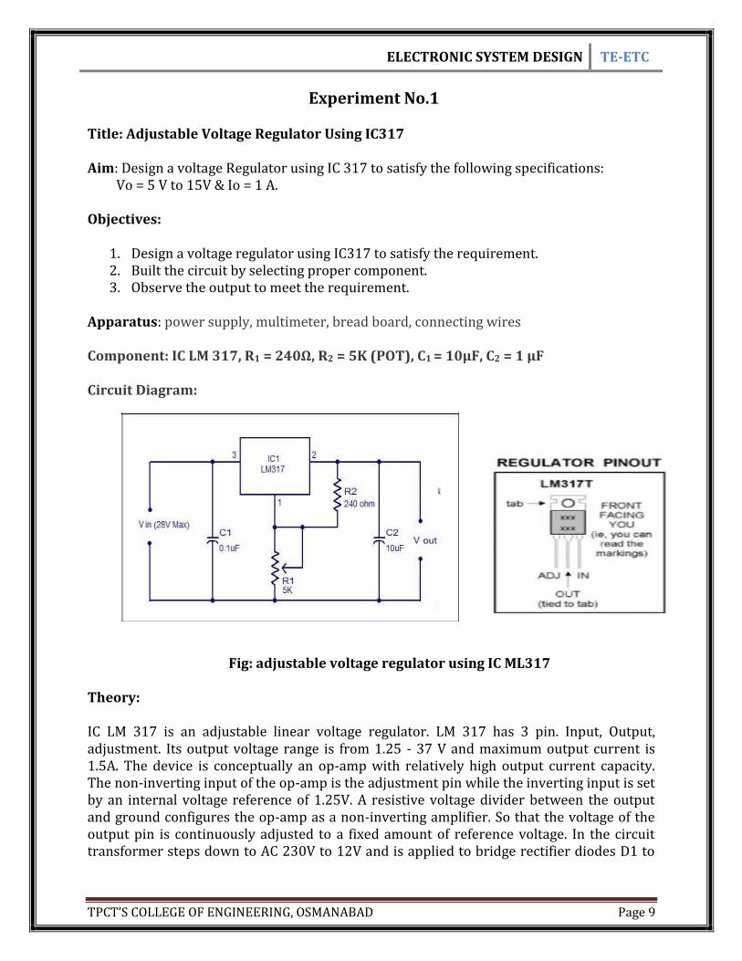
Experiment No.1 Title: Adjustable Voltage Regulator Using IC317 Aim: Design a voltage Regulator using IC 317 to satisfy the following specifications: Vo = 5 V to 15V & Io = 1 A. Objectives:
1. Design a voltage regulator using IC317 to satisfy the requirement. 2. Built the circuit by selecting proper component. 3. Observe the output to meet the requirement.
Apparatus: power supply, multimeter, bread board, connecting wires Component: IC LM 317, R1 = 240Ω, R2 = 5K (POT), C1 = 10µF, C2 = 1 µF Circuit Diagram:
Fig: adjustable voltage regulator using IC ML317 Theory: IC LM 317 is an adjustable linear voltage regulator. LM 317 has 3 pin. Input, Output, adjustment. Its output voltage range is from 1.25 - 37 V and maximum output current is 1.5A. The device is conceptually an op-amp with relatively high output current capacity. The non-inverting input of the op-amp is the adjustment pin while the inverting input is set by an internal voltage reference of 1.25V. A resistive voltage divider between the output and ground configures the op-amp as a non-inverting amplifier. So that the voltage of the output pin is continuously adjusted to a fixed amount of reference voltage. In the circuit transformer steps down to AC 230V to 12V and is applied to bridge rectifier diodes D1 to
ELECTRONIC SYSTEM DESIGN TE-ETC
TPCT’S COLLEGE OF ENGINEERING, OSMANABAD Page 10
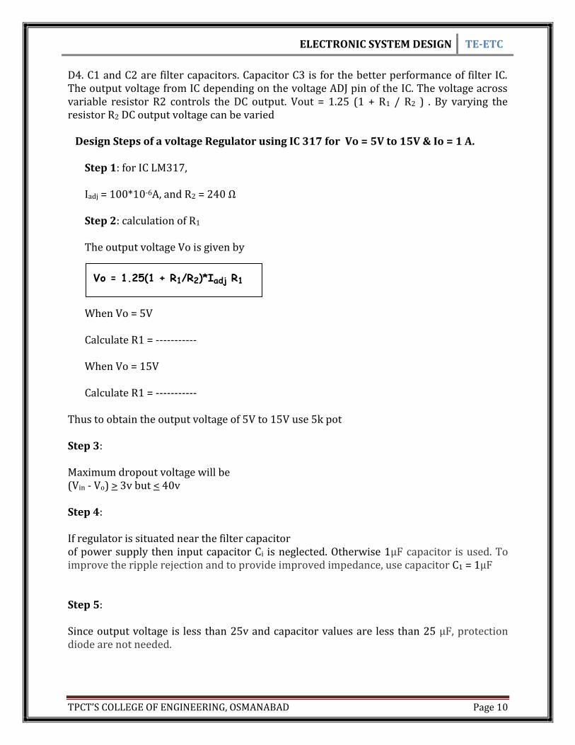
D4. C1 and C2 are filter capacitors. Capacitor C3 is for the better performance of filter IC. The output voltage from IC depending on the voltage ADJ pin of the IC. The voltage across variable resistor R2 controls the DC output. Vout = 1.25 (1 + R1 / R2 ) . By varying the resistor R2 DC output voltage can be varied Design Steps of a voltage Regulator using IC 317 for Vo = 5V to 15V & Io = 1 A.
Step 1: for IC LM317, Iadj = 100*10-6A, and R2 = 240 Ω Step 2: calculation of R1
The output voltage Vo is given by
When Vo = 5V
Calculate R1 = ----------- When Vo = 15V
Calculate R1 = -----------
Thus to obtain the output voltage of 5V to 15V use 5k pot Step 3: Maximum dropout voltage will be (Vin - Vo) > 3v but < 40v Step 4: If regulator is situated near the filter capacitor of power supply then input capacitor Ci is neglected. Otherwise 1µF capacitor is used. To improve the ripple rejection and to provide improved impedance, use capacitor C1 = 1µF Step 5: Since output voltage is less than 25v and capacitor values are less than 25 µF, protection diode are not needed.
Vo = 1.25(1 + R1/R2)*Iadj R1

ELECTRONIC SYSTEM DESIGN TE-ETC
TPCT’S COLLEGE OF ENGINEERING, OSMANABAD Page 11
Step 6: The minimum input voltage is required by regulator is Vin = Vo + dropout voltage Procedure:
1. Make the connection as per the circuit diagram 2. Vary the pot as per the values of R1 3. Observe the output to meet specification
Observation table:
Output Voltage Theoretical Value of R1
Practical Value of R1
2V
5V
10V
15 V
20 V Result:
Output voltage of regulator is adjustable from VO = 5V to 15V when pot varies between the value 0.71k Ω to 2.6 k Ω
Conclusion: Output voltage is Variable and Regulated same as per design, Hence
component selected are correct. VIVA QUESTION Q1. Which IC’S are used for voltage regulation? Q2. What are the features of IC LM317? Q3. What do you mean by voltage regulation? Q4. What are the function of input and output capacitors of regulator circuit Q5. What are the applications of voltage regulator?

ELECTRONIC SYSTEM DESIGN TE-ETC
TPCT’S COLLEGE OF ENGINEERING, OSMANABAD Page 12
Experiment No.2 Title: To design a variable gain Instrumentation Amplifier Aim: Design an Instrumentation Amplifier with variable gain of 2≤ A ≤ 2000 by means of 100KΩ pot using op-amp IC741. The signal amplitude is 15mv Objectives: To,
1. Design an Instrumentation Amplifier as per requirement 2. Built the circuit by selecting proper component. 3. Compare the output to meet the requirement.
Apparatus: Trainer kit, Power Supply, Multimeter, Connecting wires etc. Component: IC 741(03), 100K pot, fixed register 10K, 51K, 50Ω Circuit Diagram:

ELECTRONIC SYSTEM DESIGN TE-ETC
TPCT’S COLLEGE OF ENGINEERING, OSMANABAD Page 13
Theory:
Instrumentation amplifier is a kind of differential amplifier with additional input buffer stages. The addition of input buffer stages makes it easy to match (impedance matching) the amplifier with the preceding stage. Instrumentation are commonly used in industrial test and measurement application. The instrumentation amplifier also has some useful features like low offset voltage, high CMRR (Common mode rejection ratio), high input resistance, high gain etc. The circuit diagram of a typical instrumentation amplifier using op-amp is shown below.
A circuit providing an output based on the difference between two inputs (times a scale factor) is given in the above figure. In the circuit diagram, op-amps labeled A1 and A2 are the input buffers. Anyway the gain of these buffer stages are not unity because of the presence of R1 and Rg. Op amp labeled A3 is wired as a standard differential amplifier. R3 connected from the output of A3 to its non inverting input is the feedback resistor. R2 is the input resistor. The voltage gain of the instrumentation amplifier can be expressed by using the equation below.
Voltage gain (Av) = Vo/(V2-V1) = (1 + 2R1/Rg ) x R3/R2
If need a setup for varying the gain, replace Rg with a suitable potentiometer. Instrumentation amplifiers are generally used in situations where high sensitivity, accuracy and stability are required. Instrumentation amplifiers can be also made using two op-amps, but they are rarely used and the common practice is to make it using three op-amps like what is shown here. The only advantages of making an instrumentation amplifier using 2 op-amps are low cost and improved CMRR.
A high gain accuracy can be achieved by using precision metal film resistors for all the resistances. Because of large negative feedback employed, the amplifier has good linearity, typically about 0.01% for a gain less than 10. The output impedance is also low, being in the range of milli-ohms. The input bias current of the instrumentation amplifier is determined by the op-amps A1 and A2.

ELECTRONIC SYSTEM DESIGN TE-ETC
TPCT’S COLLEGE OF ENGINEERING, OSMANABAD Page 14
Design steps of an Instrumentation Amplifier with variable gain of 2≤ A ≤ 2000 by means of 100KΩ pot. Step 1: calculation of gain R3 and R2
Given that overall gain of Instrumentation Amplifier is
Let R1 = R2 = 10 KΩ, ¼ Watt.
Maximum Gain is calculated as Am = (1 +2 R3 /RGA )
1000 = (1 +2 R3 /RGA)
2R3 / RG A = 1999 ------------ (1)
Minimum Gain is calculated as Am = (1 +2 R3 / RG +RGA) 1 = (1 +2 R3 /100KΩ+RGA)
2R3 / 100KΩ+RGA = 1 2R3 = 100KΩ+RGA
Put the value of 2R3 in equation (1)
Choose RG A = 50Ω . Choose RG A = 51Ω. Hence
R3 = RGA * 1999 / 2 R3 = 50974.5 Ω Select R3 = 51 KΩ
Gain A = (1 +2 R3 /RG) (R2 /R1)

ELECTRONIC SYSTEM DESIGN TE-ETC
TPCT’S COLLEGE OF ENGINEERING, OSMANABAD Page 15
Step 2: Connect V1 & V2 input terminals & give an input DC = 15mV.
Vin DC = 15mV. Keep the pot at min and max position and measure the output voltage. Verify theoretical & practical result. Procedure:
1. Construct the instrumentation amplifier as shown in fig. using 741 op- amp 2. Apply input voltage and measure the output voltage 3. Compare practical and calculated out voltage
Calculations:
Vout (Max) = (1 +2 R3 /RG A )* Vin Vout (Min) = (1 +2 R3 /RG A + RG )* Vin
Observation Table:
Vin Vout (Max) Vout (Min) Vout (Max) Vout (Min)
Practical Practical Calculated Calculated
10mV
15mV
Result: Calculated gain: ------------- Practical gain: -------------- Conclusion: Design of variable gain instrumentation amplifier with three op-amps is done successfully. VIVA QUESTION Q1. Explain the feature of Instrumentation Amplifier Q2. What are the advantages of instrumentation amplifier using three op amp Q3. How can we calculate overall gain of instrumentation amplifier? Q4. Which IC’S are available for instrumentation amplifier? Q5. What are the industrial applications of instrumentation amplifier?
ELECTRONIC SYSTEM DESIGN TE-ETC
TPCT’S COLLEGE OF ENGINEERING, OSMANABAD Page 16
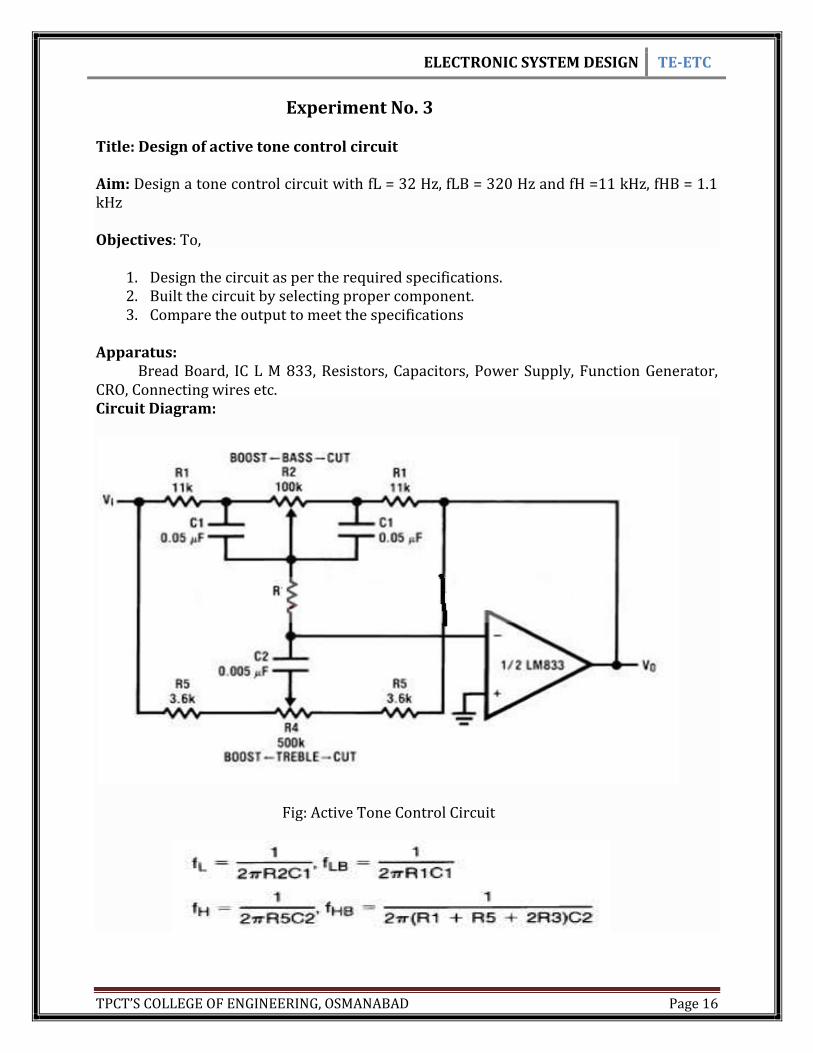
Experiment No. 3
Title: Design of active tone control circuit
Aim: Design a tone control circuit with fL = 32 Hz, fLB = 320 Hz and fH =11 kHz, fHB = 1.1 kHz
Objectives: To,
1. Design the circuit as per the required specifications. 2. Built the circuit by selecting proper component. 3. Compare the output to meet the specifications
Apparatus: Bread Board, IC L M 833, Resistors, Capacitors, Power Supply, Function Generator, CRO, Connecting wires etc. Circuit Diagram:
Fig: Active Tone Control Circuit

ELECTRONIC SYSTEM DESIGN TE-ETC
TPCT’S COLLEGE OF ENGINEERING, OSMANABAD Page 17
Theory: Using LM833 can be designed a very simple tone control circuit using few external components .For this Lm833 tone control circuit can be used almost any type of operational amplifier if it have high input impedance . The LM833 is a dual general purpose operational amplifier designed with particular emphasis on performance in audio systems. The ton control from this circuit is based on this operational amplifier from National Semiconductor and two RC filters (low pass and high pass ) .Using the formula presented bellow we can modify the frequency of the tone control circuit - the cut off frequency of RC filters (low pass and high pass ). LM833 tone control formula
Design Steps of the tone control circuit presented in this schematic the frequencies are : fL = 32 Hz, fLB = 320 Hz and fH =11 kHz, fHB = 1.1 kHz
Step 1: Given that fL = 32 Hz, R1 = 11kHΩ, R2 = 100KΩ at low frequency f < fL, gain magnitude AB can be varied over range
R1
R1+ R2 < AB <
R1+ R2
R1
By means of pot used for bass control
FL = 1
2𝜋𝑅2𝐶1
calculate values of capacitance C1 Step 2: Given fH =11 kHz, R3 = 3.6 K, R4 = 500 KΩ, For frequency f > fH
Gain at varied over range
𝑅3
𝑅1+𝑅3+2𝑅5 < AT <
𝑅1+𝑅3+2𝑅5
𝑅3
fH = 1
2𝜋𝑅3𝐶12
Calculate the values Procedure:
1. Design the circuit using given formulae.

ELECTRONIC SYSTEM DESIGN TE-ETC
TPCT’S COLLEGE OF ENGINEERING, OSMANABAD Page 18
2. Implement the circuit as shown in the circuit diagram. 3. Vary the input frequency & measure the output voltage. 4. Calculate the gain and bandwidth
Observation table:
Sr.no
frequency Output voltage gain
1
2
3
.
15
Frequency Response Curve: vol f1 f2 freq Result:
1. Treble frequency: F2 = ----------- 2. Bass frequency: F1 = ----------- 3. Bandwidth(F2- F1): = -------------
Conclusion: The tone control circuit designed as per the specification successfully VIVA QUESTION Q1. What are drawbacks of passive tone control circuit? Q2. Which IC’S are available for tone control circuit? Q3. What do you mean by Bass and Treble? Q4. What are the features of IC LM833 Q5. What are the applications of tone control circuit?
ELECTRONIC SYSTEM DESIGN TE-ETC
TPCT’S COLLEGE OF ENGINEERING, OSMANABAD Page 19
Experiment No. 4
Title: Design of an Audio power amplifier using LM380 Aim: To Design audio power amplifier using LM380 for following specification, PO = 1.5W, RL = 4Ω, BW = 30 to 15 KHz, Av = 50 Objectives: To,
1. Design the circuit as per the required specifications. 2. Built the circuit by selecting proper component. 3. Compare the output to meet the specifications
Apparatus: Bread Board, IC LM 380, Speaker, Power Supply, Function Generator,
CRO, Connecting wires etc. Component: RC = 2.7 Ω CC = 0.1µf, C1 = 500 µf, C2 = 24 µf, R1 = 1M Ω, R2 = 15.2K Ω,
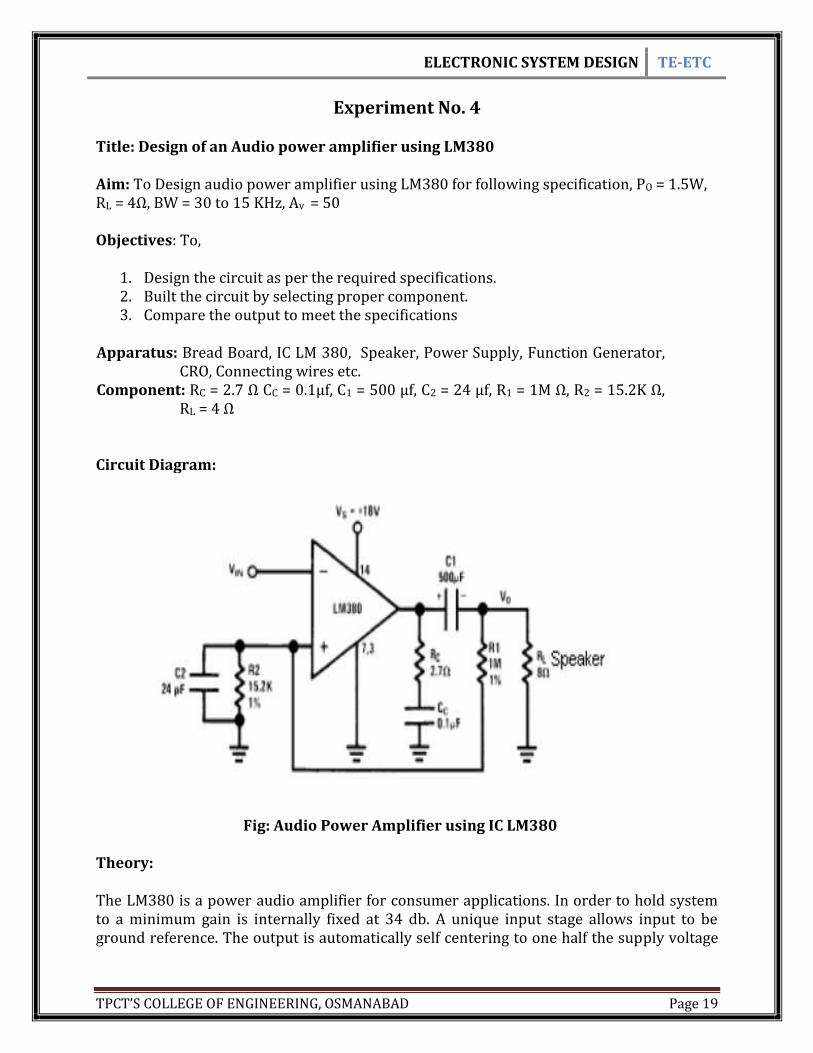
RL = 4 Ω Circuit Diagram:
Fig: Audio Power Amplifier using IC LM380 Theory: The LM380 is a power audio amplifier for consumer applications. In order to hold system to a minimum gain is internally fixed at 34 db. A unique input stage allows input to be ground reference. The output is automatically self centering to one half the supply voltage

ELECTRONIC SYSTEM DESIGN TE-ETC
TPCT’S COLLEGE OF ENGINEERING, OSMANABAD Page 20
the output is short circuit proof with internal thermal limiting. The package outline is standard dual in line package a copper lead frame is used with the center three pins on either side comprising a heat sink. This makes the device easy to use in standard pc layout. Uses include simple phonograph amplifier, intercoms, line drivers, teaching machine output, alarms ultrasonic drivers, TV sound system, AM- FM radio, small servo drivers, power convertors, etc. The variable gains up to 50 are obtained by use of potentiometer across the two input terminals as shown in figure. At the output of amplifier a speaker of 8 Ω is connected through a coupling capacitor of 500 µF to suppress undesirable oscillations RC network is connected at output with 2.7Ω and 0.1 µF. FEATURE:
Wide supply voltage range Low quiescent power drain Voltage gain fixed at 50 High peak current capability Input referenced to Gnd High input impedance Low distortion Quiescent output voltage is at one-half of the supply voltage Standard Dual in line package
Fig: LM 380 for variable gain 50
ELECTRONIC SYSTEM DESIGN TE-ETC
TPCT’S COLLEGE OF ENGINEERING, OSMANABAD Page 21
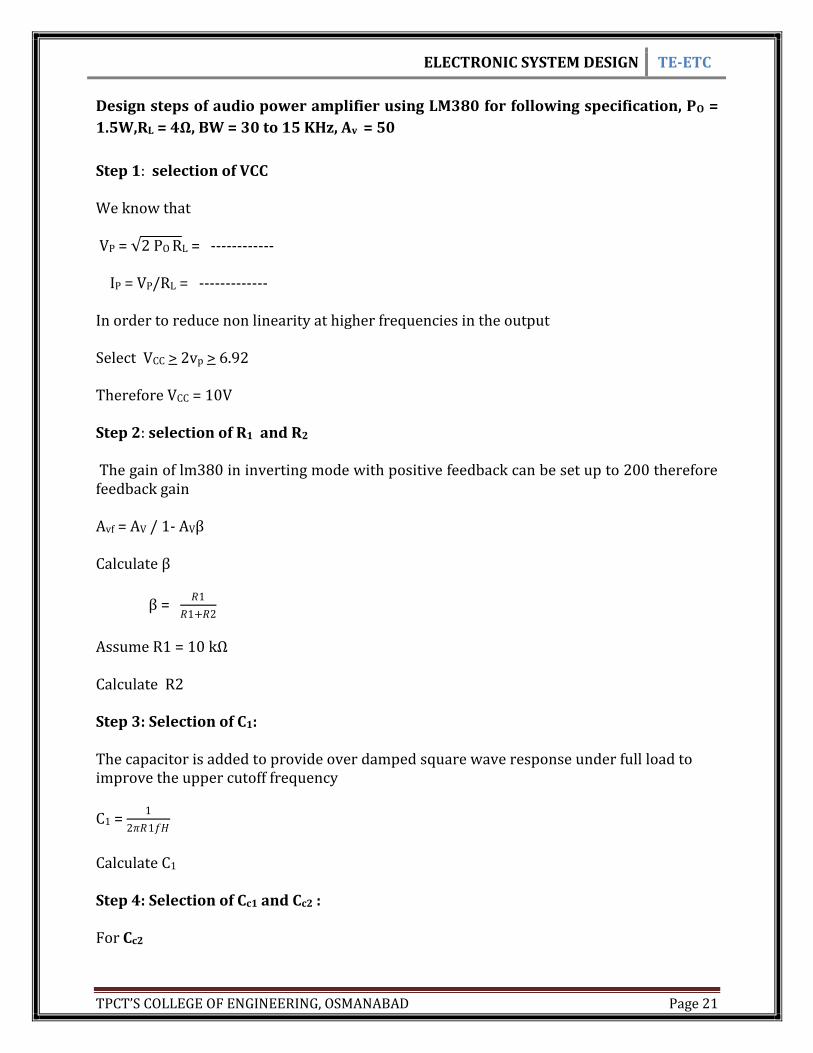
Design steps of audio power amplifier using LM380 for following specification, PO =
1.5W,RL = 4Ω, BW = 30 to 15 KHz, Av = 50
Step 1: selection of VCC We know that VP = √2 PO RL = ------------ IP = VP/RL = ------------- In order to reduce non linearity at higher frequencies in the output Select VCC > 2vp > 6.92 Therefore VCC = 10V Step 2: selection of R1 and R2
The gain of lm380 in inverting mode with positive feedback can be set up to 200 therefore feedback gain Avf = AV / 1- AVβ Calculate β
β = 𝑅1
𝑅1+𝑅2
Assume R1 = 10 kΩ Calculate R2 Step 3: Selection of C1: The capacitor is added to provide over damped square wave response under full load to improve the upper cutoff frequency
C1 = 1
2𝜋𝑅1𝑓𝐻
Calculate C1
Step 4: Selection of Cc1 and Cc2 : For Cc2

ELECTRONIC SYSTEM DESIGN TE-ETC
TPCT’S COLLEGE OF ENGINEERING, OSMANABAD Page 22
Cc2 = 1
2𝜋𝑅𝐿𝑓𝐿
For Cc1
Cc1 = 1
2𝜋𝑅𝑖𝑓𝐿
The input impedance of LM380 is 150 kΩ (Use Ri = 150 kΩ) Step 5: Selection of C3 and R3 : Upper cut off frequency attenuation due to noise can be improved by a series combination R3- C3 , places at the output of the amplifier it also eliminates 5 to 10MHz small amplitude oscillation in RF sensitive environment use C3 = 0.1µF and R3 = 2.7Ω Step 6: Selection of VCC: For VCC or 5 to 8v use C2 = 0.1 µF filter capacitor to avoid spikes in supply voltage. Procedure:
1. Assemble the circuit as per the circuit diagram 2. Give a Sine wave input of 10 mV peak to peak at the input. 3. Vary the frequency measure the output 4. Calculate the gain and bandwidth
Observation table:
Sr.no
frequency Output voltage gain
1
2
3
.
.
.
15
ELECTRONIC SYSTEM DESIGN TE-ETC
TPCT’S COLLEGE OF ENGINEERING, OSMANABAD Page 23
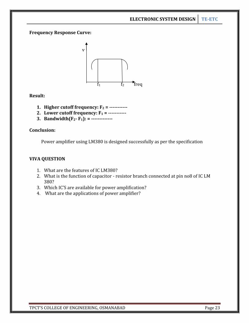
Frequency Response Curve: v f1 f2 freq Result:
1. Higher cutoff frequency: F2 = ----------- 2. Lower cutoff frequency: F1 = ----------- 3. Bandwidth(F2- F1): = -------------
Conclusion: Power amplifier using LM380 is designed successfully as per the specification VIVA QUESTION
1. What are the features of IC LM380? 2. What is the function of capacitor - resistor branch connected at pin no8 of IC LM
380? 3. Which IC’S are available for power amplification? 4. What are the applications of power amplifier?
ELECTRONIC SYSTEM DESIGN TE-ETC
TPCT’S COLLEGE OF ENGINEERING, OSMANABAD Page 24
Experiment No. 5
Title: Design of an AM detector
Aim: design a diode detector circuit for AM wave with following specifications Ri = 10kΩ, fm = 5kHz, fc = 550 k Hz
Objectives: To,
1. Design the circuit as per the required specifications. 2. Built the circuit by selecting proper component. 3. Compare the output to meet the specifications
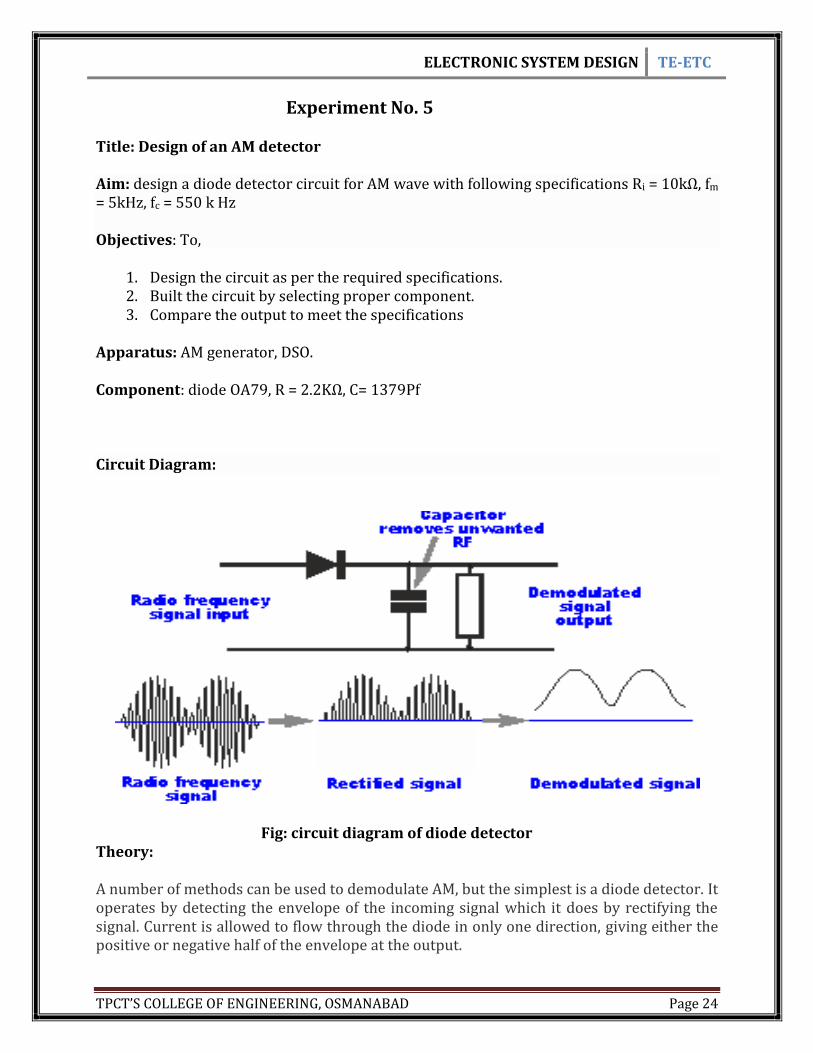
Apparatus: AM generator, DSO. Component: diode OA79, R = 2.2KΩ, C= 1379Pf Circuit Diagram:
Fig: circuit diagram of diode detector Theory: A number of methods can be used to demodulate AM, but the simplest is a diode detector. It operates by detecting the envelope of the incoming signal which it does by rectifying the signal. Current is allowed to flow through the diode in only one direction, giving either the positive or negative half of the envelope at the output.

ELECTRONIC SYSTEM DESIGN TE-ETC
TPCT’S COLLEGE OF ENGINEERING, OSMANABAD Page 25
If the detector is to be used only for audio detection it does not matter which half of the envelope is used, either will work equally well. Only when the detector is also used to supply the automatic gain control (AGC) circuitry will the polarity of the diode matter.
The AM detector or demodulator includes a capacitor at the output. Its purpose is to remove any radio frequency components of the signal at the output. The value is chosen so that it does not affect the audio base-band signal. There is also a leakage path to enable the capacitor to discharge, but this may be provided by the circuit into which the demodulator is connected.
Simple AM diode detector circuit
This type of detector or demodulator is called a linear envelope detector because the output is proportional to the input envelope.
DC return required
In order for a diode detector to generate the required DC voltage, a DC return must be available within the circuit. supplied.
This can be achieved by placing an RF choke across the input to the detector diode. This appears like an open circuit to radio frequency signals, but acts as a DC return path for the audio and other signals appearing from the detector.
Diode detector with DC return
Often this DC return path may be within a transformer used to drive the diode detector. Alternatively a resistor may be used. It value will be the same at all frequencies and therefore its choice is a matter of compromise.
Diode detector advantages & disadvantages
The diode detector is widely sued, but it has several advantages and disadvantages:
Diode detector advantages
Simplicity: The diode detector is very simple and is easy to construct. The circuit six very straightforward, consisting of a very few components.

ELECTRONIC SYSTEM DESIGN TE-ETC
TPCT’S COLLEGE OF ENGINEERING, OSMANABAD Page 26
Low cost: Requiring so few components, and the fact that he components are not specialised, this form of detector is very cheap. Accordingly it is widely used in AM domestic radios.
Diode detector disadvantages
Distortion: Although the diode detector is able to operate in a reasonably linear fashion over a reasonable range, outside this range high levels of distortion are introduced, and even within the more linear range, distortion levels are not particularly low. It is adequate for small low cost radios.
Selective fading: These detectors are susceptible to the effects of selective fading experienced on short wave broadcast transmissions. Here the ionospheric propagation may be such that certain small bands of the signal are removed. Under normal circumstances signals received via the ionosphere reach the receiver via a number of different paths. The overall signal is a combination of the signals received via each path and as a result they will combine with each other, sometimes constructively to increase the overall signal level and sometimes destructively to reduce it. It is found that when the path lengths are considerably different this combination process can mean that small portions of the signal are reduced in strength. An AM signal consists of a carrier with two sidebands
Insensitive: Semiconductor diodes have a certain turn-on voltage. Accordingly the voltage has to reach a certain level before the diode is able to operate reasonably efficiently.
Design steps of a diode detector circuit for AM wave with following specifications Ri = 10kΩ, fm = 5kHz, fc = 550 k Hz Step 1: selection of diode Foe AM detector point contact diode detector OA79 is used which has following specifications, Reverse voltage = 45v, IP = 35 mA, VP = 0.3v Rectification efficiency = 85, Damping resistance = 15K Ω. Step2: calculation of R and C To meet the requirement of diode detector without diagonal peak clipping for 100% modulation use equation RC = √1/ωm ωc Since the value of Ri > > R select R = 2.2k Ω, calculate the value of c Procedure:
1. Built the circuit as per the circuit diagram.
ELECTRONIC SYSTEM DESIGN TE-ETC
TPCT’S COLLEGE OF ENGINEERING, OSMANABAD Page 27
2. Observe the output on DSO. 3. Verify the frequency of demodulated signal.
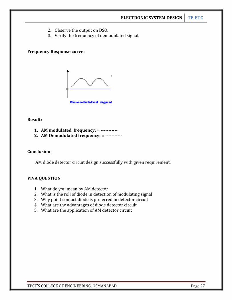
Frequency Response curve:
Result:
1. AM modulated frequency: = ----------- 2. AM Demodulated frequency: = -----------
Conclusion: AM diode detector circuit design successfully with given requirement. VIVA QUESTION
1. What do you mean by AM detector 2. What is the roll of diode in detection of modulating signal 3. Why point contact diode is preferred in detector circuit 4. What are the advantages of diode detector circuit 5. What are the application of AM detector circuit

ELECTRONIC SYSTEM DESIGN TE-ETC
TPCT’S COLLEGE OF ENGINEERING, OSMANABAD Page 28
Experiment No.6
Title: Design of IC based counter circuit Aim : To design Divide by 6 counter using IC7490
Objectives: To,
1. Design the circuit as per the required specifications. 2. Built the circuit by selecting proper component. 3. Compare the output to meet the specifications
Apparatus : Power Supply, Digital Trainer kit, IC 7490,Connecting Wires, CircuitDiagram :
Fig: Circuit Diagram of Decade counter
Theory: The 74LS90 BCD Counter
The 74LS90 integrated circuit is basically a MOD-10 decade counter that produces a BCD output code. The 74LS90 consists of four master-slave JK flip-flops internally connected to provide a MOD-2 (count-to-2) counter and a MOD-5 (count-to-5) counter. The 74LS90 has one independent toggle JK flip-flop driven by the CLK A input and three toggle JK flip-flops that form an asynchronous counter driven by the CLK B input as shown.
1
12 9 8 1 11
14
2 3
IC 7490
A
Clock i/p
B
10 7
S1 S2 R1 R2
Q0 Q1 Q2 Q3

ELECTRONIC SYSTEM DESIGN TE-ETC
TPCT’S COLLEGE OF ENGINEERING, OSMANABAD Page 29
74LS90 BCD Counter
The counters four outputs are designated by the letter symbol Q with a numeric subscript equal to the binary weight of the corresponding bit in the BCD counter circuits code. So for example, QA, QB, QC and QD. The 74LS90 counting sequence is triggered on the negative going edge of the clock signal, that is when the clock signal CLK goes from logic 1 (HIGH) to logic 0 (LOW).
The additional input pins R1 and R2 are counter “reset” pins while inputs S1 and S2 are “set” pins. When connected to logic 1, the Reset inputs R1 and R2 reset the counter back to zero, 0 (0000), and when the Set inputs S1 and S2 are connected to logic 1, they Set the counter to maximum, or 9 (1001) regardless of the actual count number or position.
As we said before, the 74LS90 counter consists of a divide-by-2 counter and a divide-by-5 counter within the same package. Then we can use either counter to produce a divide-by-2 frequency counter only, a divide-by-5 frequency counter only or the two together to produce our desired divide-by-10 BCD counter.

ELECTRONIC SYSTEM DESIGN TE-ETC
TPCT’S COLLEGE OF ENGINEERING, OSMANABAD Page 30
. 74LS90 Divide-by-10 Counter
Then we can see that BCD counters are binary counters that count from 0000 to 1001 and then resets as it has the ability to clear all of its flip-flops after the ninth count. If we connect a pushbutton switch (SW1) to clock input CLKA, each time the pushbutton switch is released the counter will count by one. If we connected light emitting diodes (LED’s) to the output terminals, QA, QB, QC and QD as shown, we can view the binary coded decimal count as it takes place.
Design Steps for Divide by 6 counter using IC7490 1. The mod-6 counter should count the following state 0-1-2-3-4-5 and will reset after
6(0110). 2. To obtain divide by 6 counter, IC 7490 will be connected to count for normal binary
sequences i.e. clock signal is applied to input B and Q0 is connected to input B 3. To have reset at state 6(0110) the reset R1 and R 2 are connected to output Q2,and Q3
as soon as Q2 = Q3 the circuit will reset to 0000 .
Procedure :
1. According to pin assignment built the circuit
2. Apply the clock pulses
3. Count the sequence and compare the result

ELECTRONIC SYSTEM DESIGN TE-ETC
TPCT’S COLLEGE OF ENGINEERING, OSMANABAD Page 31
Truth table:
Clock pulses
Q0 Q1 Q2 Q3
0 0 0 0 0 1 0 0 0 1 2 0 0 1 0 3 0 0 1 1 4 0 1 0 0 5 0 1 0 1 6 0 0 0 0
Result: The counter count the sequence from 0 to 5 and after that it will be reset Conclusion: MOD-6 counter using IC7490 is designed successfully. VIVA QUESTION
1. List the counter IC’S available with their feature 2. Is IC7490 synchronous or asynchronous IC, justifying your answer? 3. What is the circuit modification if we design the MOD-5 counter using 7490? 4. How many counter we can design using single IC7490? 5. What are the applications of counter?
ELECTRONIC SYSTEM DESIGN TE-ETC
TPCT’S COLLEGE OF ENGINEERING, OSMANABAD Page 32
Experiment No 7
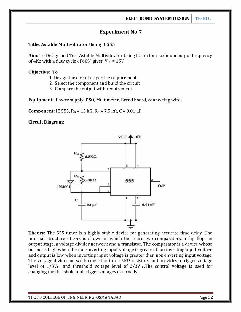
Title: Astable Multivibrator Using IC555 Aim: To Design and Test Astable Multivibrator Using IC555 for maximum output frequency of 4Kz with a duty cycle of 60% given VCC = 15V Objective: To, 1. Design the circuit as per the requirement. 2. Select the component and build the circuit 3. Compare the output with requirement Equipment: Power supply, DSO, Multimeter, Bread board, connecting wires Component: IC 555, RB = 15 kΩ, RA = 7.5 kΩ, C = 0.01 µF Circuit Diagram:
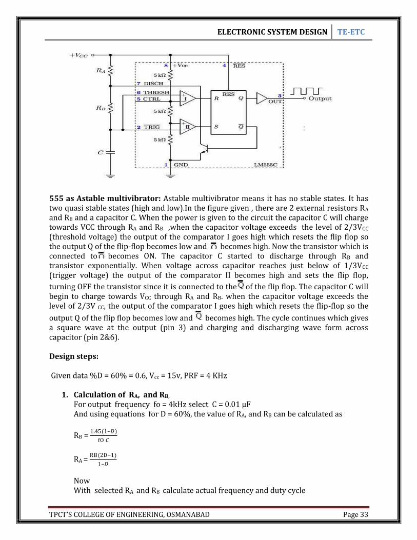
Theory: The 555 timer is a highly stable device for generating accurate time delay .The internal structure of 555 is shown in which there are two comparators, a flip flop, an output stage, a voltage divider network and a transistor. The comparator is a device whose output is high when the non-inverting input voltage is greater than inverting input voltage and output is low when inverting input voltage is greater than non-inverting input voltage. The voltage divider network consist of three 5KΩ resistors and provides a trigger voltage level of 1/3VCC and threshold voltage level of 2/3VCC.The control voltage is used for changing the threshold and trigger voltages externally.
ELECTRONIC SYSTEM DESIGN TE-ETC
TPCT’S COLLEGE OF ENGINEERING, OSMANABAD Page 33
555 as Astable multivibrator: Astable multivibrator means it has no stable states. It has two quasi stable states (high and low).In the figure given , there are 2 external resistors RA and RB and a capacitor C. When the power is given to the circuit the capacitor C will charge towards VCC through RA and RB ,when the capacitor voltage exceeds the level of 2/3VCC (threshold voltage) the output of the comparator I goes high which resets the flip flop so the output Q of the flip-flop becomes low and becomes high. Now the transistor which is connected to becomes ON. The capacitor C started to discharge through RB and transistor exponentially. When voltage across capacitor reaches just below of 1/3VCC (trigger voltage) the output of the comparator II becomes high and sets the flip flop,
turning OFF the transistor since it is connected to the of the flip flop. The capacitor C will begin to charge towards VCC through RA and RB. when the capacitor voltage exceeds the level of 2/3V CC, the output of the comparator I goes high which resets the flip-flop so the
output Q of the flip flop becomes low and becomes high. The cycle continues which gives a square wave at the output (pin 3) and charging and discharging wave form across capacitor (pin 2&6). Design steps: Given data %D = 60% = 0.6, Vcc = 15v, PRF = 4 KHz
1. Calculation of RA, and RB, For output frequency fo = 4kHz select C = 0.01 µF And using equations for D = 60%, the value of RA, and RB can be calculated as
RB = 1.45(1−𝐷)
fO 𝐶
RA = RB(2D−1)
1−𝐷
Now With selected RA and RB calculate actual frequency and duty cycle

ELECTRONIC SYSTEM DESIGN TE-ETC
TPCT’S COLLEGE OF ENGINEERING, OSMANABAD Page 34
2. Calculation of actual frequency:
fO = 1.45
(𝑅𝐴+2𝑅𝐵)𝐶
3. Calculation of actual duty cycle:
%D = (𝑅𝐴+𝑅𝐵)
𝑅𝐴+2𝑅𝐵) X 100
Procedure:
1. Built the circuit as per the circuit diagram. 2. Compare the practical result with required specification.
Result: Theoretical frequency = --------------- Practical frequency = --------------- Conclusion: Astable multivibrator can be design successfully as per the circuit diagram VIVA QUESTION
1. What are the features of IC555? 2. What do you mean by multivibrator? Enlist their types? 3. What are applications of IC555? 4. What are applications of multivibrator? 5. Can we design monostable multivibrator using IC555? What is the circuit
modification?
ELECTRONIC SYSTEM DESIGN TE-ETC
TPCT’S COLLEGE OF ENGINEERING, OSMANABAD Page 35
Experiment No.8
Aim: To Study Data Acquisition System for parameters like : Temperature, Pressure,
Light. Theory:
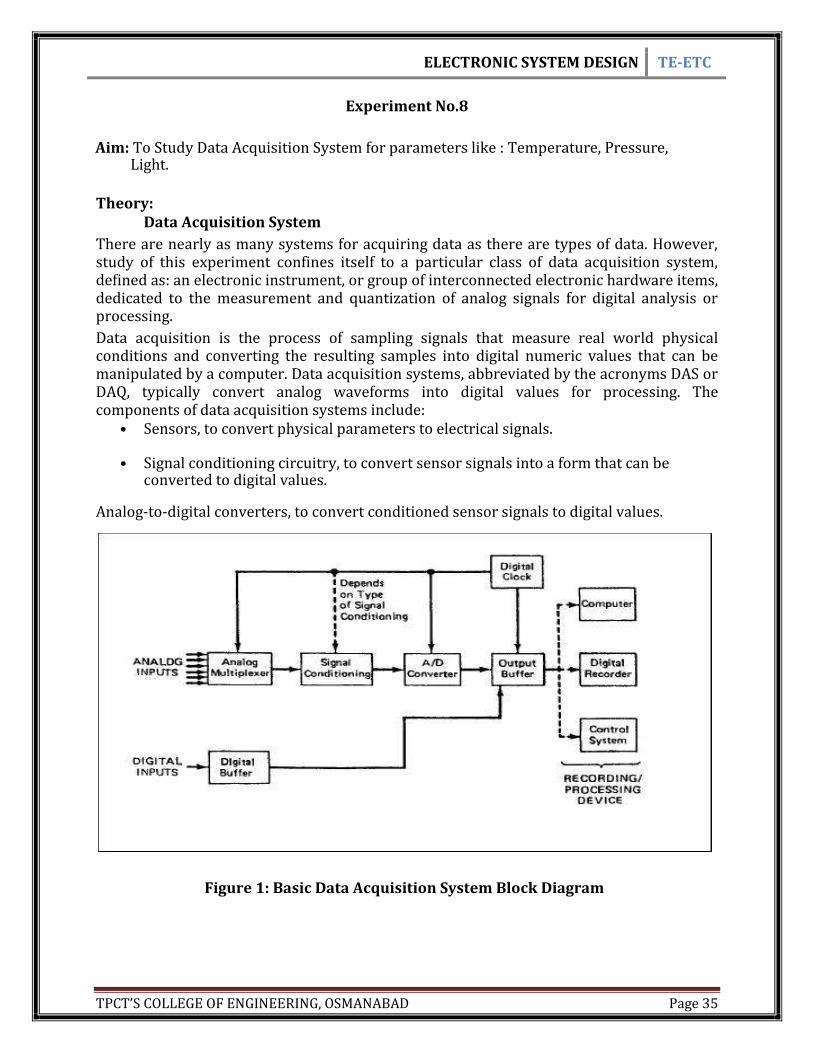
Data Acquisition System There are nearly as many systems for acquiring data as there are types of data. However, study of this experiment confines itself to a particular class of data acquisition system, defined as: an electronic instrument, or group of interconnected electronic hardware items, dedicated to the measurement and quantization of analog signals for digital analysis or processing. Data acquisition is the process of sampling signals that measure real world physical conditions and converting the resulting samples into digital numeric values that can be manipulated by a computer. Data acquisition systems, abbreviated by the acronyms DAS or DAQ, typically convert analog waveforms into digital values for processing. The components of data acquisition systems include:
• Sensors, to convert physical parameters to electrical signals.
• Signal conditioning circuitry, to convert sensor signals into a form that can be converted to digital values.
Analog-to-digital converters, to convert conditioned sensor signals to digital values.
Figure 1: Basic Data Acquisition System Block Diagram

ELECTRONIC SYSTEM DESIGN TE-ETC
TPCT’S COLLEGE OF ENGINEERING, OSMANABAD Page 36
Analog Multiplexer: The analog multiplexer permits a number of signal sources to be automatically measured by the same data acquisition hardware. It consists of a series of switches whose inputs are tied to the various analog signals and whose outputs are tied to a common measuring point. Each input is individually connected to the measuring point in a predetermined sequence. The number of channels in a multiplexer may vary from two to several hundred. Signal Conditioning: Very often the signals presented to the inputs of the data acquisition system are not in a form appropriate for conversion, and so they must be preconditioned. The required signal conditioning could consist of linear amplification, logarithmic amplification, filtering, peak detection, or sample-and-hold. Often more than one of these functions is acquired. For instance, it is not uncommon to combine amplification with filtering or to find a low-level amplifier before a sample-and-hold. Analog-to-Digital (A/D) Converter The analog to digital converter actually translates the analog signal into an encoded digital format. Of the numerous ways to perform this function, only about half-dozen techniques have found wide acceptance. Most notable are the dual-slope integrating and the successive approximation converters. A/D converters are often referred to by the number of output digits they produce. In a binary system, the range is from 4 to 16 bits, while in a binary-coded decimal system, 3 to 4 digits are normal. Digital Clock
The digital clock provides the master timing for the data acquisition system. It may be as simple as a multi phased crystal controlled oscillator, or it may provide the user with a wide selection of multiplexer rates and modes of operation. Some systems also contain both time-of-day and day-of-year clocks
Manual Data Entry Many data acquisition systems provide users with a way to tag the data they are accumulating, through some sort of manual data entry. They may wish to note such things as the type of data,
Digital Buffer
The ability to record discrete events is often a requirement of a data acquisition system. Since these events are usually accompanied by the opening or closing of a switch, they represent a digital input. Out-of-tolerance conditions or some other situations that might invalidate the data collection are most often designated as "discrete events."
Output Buffer The output buffer acts as the data collector for the DAS. In an ordered sequence, it gathers up such data as the multiplexer channel number, the signal conditioner gain, A/D
ELECTRONIC SYSTEM DESIGN TE-ETC
TPCT’S COLLEGE OF ENGINEERING, OSMANABAD Page 37
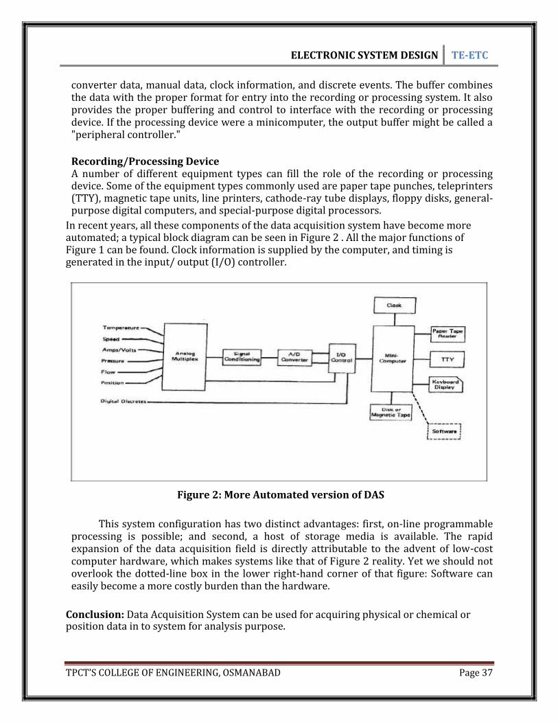
converter data, manual data, clock information, and discrete events. The buffer combines the data with the proper format for entry into the recording or processing system. It also provides the proper buffering and control to interface with the recording or processing device. If the processing device were a minicomputer, the output buffer might be called a "peripheral controller."
Recording/Processing Device A number of different equipment types can fill the role of the recording or processing device. Some of the equipment types commonly used are paper tape punches, teleprinters (TTY), magnetic tape units, line printers, cathode-ray tube displays, floppy disks, general-purpose digital computers, and special-purpose digital processors.
In recent years, all these components of the data acquisition system have become more automated; a typical block diagram can be seen in Figure 2 . All the major functions of Figure 1 can be found. Clock information is supplied by the computer, and timing is generated in the input/ output (I/O) controller.
Figure 2: More Automated version of DAS
This system configuration has two distinct advantages: first, on-line programmable
processing is possible; and second, a host of storage media is available. The rapid expansion of the data acquisition field is directly attributable to the advent of low-cost computer hardware, which makes systems like that of Figure 2 reality. Yet we should not overlook the dotted-line box in the lower right-hand corner of that figure: Software can easily become a more costly burden than the hardware.
Conclusion: Data Acquisition System can be used for acquiring physical or chemical or position data in to system for analysis purpose.

ELECTRONIC SYSTEM DESIGN TE-ETC
TPCT’S COLLEGE OF ENGINEERING, OSMANABAD Page 38
Experiment No. 9 Title: Mini Project Aim: To design and test the mini project Design steps:
Choose a real time application based electronic circuit as your mini project
Understand the concept and working of the selected topic.
Select all required components and go through its data manuals
Prepare PCB Layout
According to layout Carry out etching and drilling
Mount the components.
Fix the component by Soldering.
Test the circuit at various points and verify its function.
Format for report Title of the project:
Circuit diagram:
List of component used:
Design methodology :
Applications:
Testing procedure:
Total cost of project:
Result: (result based on circuit diagram, Prepare observation table, Draw waveforms if
applicable)
Conclusion:
Future scope:
References:
VIVA QUESTION
1. How do you make a manual PCB lay out?
2. How do you transfer the PCB layout on PCB.
3. How do you carry out PCB etching?
4. Explain drilling, component mounting and soldering procedure.
ELECTRONIC SYSTEM DESIGN TE-ETC
TPCT’S COLLEGE OF ENGINEERING, OSMANABAD Page 39
3.Quiz on the subject:
1) What are the selection criteria of transformer?
2) Dow can we design dual power supply using 78xx series
3) What are the ideal characteristics of op-amp
4) What are the industrial applications of Instrumentation amplifier?
5) What are the merits of active tone control circuit over passive tone control circuit?
6) Explain design steps of audio power amplifier using LM 380.
7) What is difference between synchronous and asynchronous counter.
8) What are the steps to design PCB.
9) How to design symmetric Astable multivibrator
10) What are the advantages of diode detector circuit
4. Conduction of VIVA-VOCE Examinations : - Teacher should conduct oral exams of the students with full preparation. Normally the objective questions with guess are to be avoided. To make it meaningful, the questions should be such that depth of the student in the subject is tested. Oral Exams are to be conducted in co-cordial situation. Teachers taking oral exams should not have ill thoughts about each other & courtesies should be offered to each other in case of opinion, which should be critically suppressed in front of the students.
5. Evaluation and marking system: - Basic honesty in the evaluation and marking system is essential and in the process impartial nature of the evaluator is required in the exam system. It is a primary responsibility of the teacher to see that right students who really put their effort &intelligence are correctly awarded. The marking pattern should be justifiable to the students without any ambiguity and teacher should see that students are faced with just circumstance.