electronic devices: transistors in si, sige, ge, iii-vs ... · pdf fileelectronic devices:...
TRANSCRIPT

MTL ANNUAL RESEARCH REPORT 2014 Electronic Devices 25
Electronic Devices: Transistors in Si, SiGe, Ge, III-Vs, GaN, and 2D MaterialsAn Efficient Bayesian Framework for Accurate Parameter Extraction from Limited Measurements ..................................27Enhanced Hole Ballistic Velocity in Germanium Nanowire p-MOSFETs Through Asymmetric Strain ............................. 28Strained-Si/strained-Ge Heterostructure Bilayer TFETs ...........................................................................................................29A Self-aligned InGaAs Quantum-well MOSFET Fabricated by a Scalable Tight-pitch Process ........................................ 30Double-gate InGaAs MOSFET for Fin-sidewall Characterization .............................................................................................31Nano-scale Metal Contacts for III-V MOSFETs .........................................................................................................................32Nanometer-scale Reactive Ion Etching of InGaAs for 3-D III-V MOSFETs ..........................................................................33InGaAs/GaAsSb Quantum-well Tunnel-FETs ............................................................................................................................. 34High-voltage Vertical GaN Diodes on Si Substrates ...................................................................................................................35Effect of Surface Pre-treatments on Ohmic Contact Resistance in AlGaN/GaN Transistors ............................................ 36Performance Limits of Large-periphery GaN Power Amplifiers ................................................................................................37Design of RF GaN HEMT Power Amplifier using MIT Virtual Source GaNFET-RF Model ................................................ 38Thermal Characterization of GaN-based Electronics ................................................................................................................. 39A Stress/Characterization Strategy to Assess the Electrical Reliability of High-voltage GaN Field-effect Transistors ...40Structural Degradation of GaN HEMTs under High-power and High-temperature Stress ................................................. 41Threshold Voltage Instability in GaN Power Field-effect Transistors ........................................................................................ 42Current-voltage Model for Graphene Solution-gated Field-effect Transistors...................................................................... 43An Ambipolar Virtual-source-based Charge-current Compact Model for Nanoscale Graphene Transistors ................... 44Graphene-MoS2 Hybrid Technology for Large-scale Two-dimensional Electronics .............................................................. 45High-performance WSe2 CMOS Devices and Integrated Circuits ......................................................................................... 46

26 Electronic Devices MTL ANNUAL RESEARCH REPORT 2014

MTL ANNUAL RESEARCH REPORT 2014 Electronic Devices 27
An Efficient Bayesian Framework for Accurate Parameter Extraction from Limited MeasurementsL. Yu, D.A. Antoniadis, D.S. Boning Sponsorship: MIT/Masdar Institute of Science and Technology
The first of our two projects is to develop methods for application to post-silicon performance estimation using the MIT virtual source mode (MVS) model. We have achieved a new performance estimation algorithm through physical subspace projection and maximum a posteriori (MAP) estimation. Our goal is to estimate the distribution of a target circuit performance with an extra-small number of measurement samples from on-chip monitor circuits. The key idea in this work is to exploit the fact that simulation and measurement data are physically correlated under different circuit configurations and topologies. First, different populations of measurements are projected to a subspace expanded by a set of physical variables. The projection is achieved by performing a sensitivity analysis of measurement parameters on subspace variables using the virtual source compact model. Then we develop a Bayesian treatment by introducing prior distributions over these projected variables. MAP estimation is also applied using the prior, as illustrated in Figure 1. The proposed method has been validated by post-silicon measurement of a commercial 28-nm process. An average error reduction of 2x is achieved, which can be translated to a 32x-reduction of the number of data
points needed for samples on the same die. A 150x and 70x sample size reduction on training dies is also achieved compared to the traditional least-square training method and least-angle regression method, respectively, without surrendering accuracy
Our second effort is a novel MOSFET parameter extraction method to enable early technology evaluation. The distinguishing feature of the proposed method is that it enables the extraction of an entire set of MOSFET model parameters using limited and incomplete IV measurements from on-chip monitor circuits, as Figure 2 shows. An important step in this method is the use of maximum-a-posteriori estimation where past measurements of transistors from various technologies are used to learn a prior distribution and its uncertainty matrix for the parameters of the target technology. The framework then utilizes Bayesian inference to facilitate extraction using a very small set of additional measurements. The proposed method is validated using various past technologies and post-silicon measurements for a commercial 28-nm process. The proposed extraction could also be used to characterize the statistical variations of MOSFETs with the significant benefit that the constraints required by the backward propagation of variance method are relaxed.
Figure 1: Illustration of sequential Bayesian learning of physi-cal subspace (threshold voltage) from prior and on-chip monitor circuits.
Figure 2: MVS model fitting results in four technologies in the 14-nm to 45-nm generations. Blue circles are fitted measure-ments using the MAP method; red circles are test measurements for validation.
FURTHER READING
• L. Yu et al. “Efficient Performance Estimation with Very Small Sample Size via Physical Subspace Projection and Maximum A Posteriori Estimation,” Design, Automation and Test in Europe (DATE), Mar. 2014.
• L. Yu et al. “Remembrance of Transistors Past: Compact Model Parameter Extraction Using Bayesian Inference and Incomplete New Mea-surements,” Design Automation Conference (DAC), June, 2014.

28 Electronic Devices MTL ANNUAL RESEARCH REPORT 2014
Enhanced Hole Ballistic Velocity in Germanium Nanowire p-MOSFETs Through Asymmetric StrainJ. Teherani, W. Chern, D. Antoniadis, J.L. Hoyt Sponsorship: NSF Center for Energy Efficient Electronics Science
Germanium has the highest hole mobility of any bulk semiconductor, and compressive biaxial strain has been used to increase the Ge hole mobility. Recent-ly, asymmetrically strained Ge nanowire p-MOSFETs exhibiting hole mobility enhancement over biaxially strained structures have been fabricated. This work studies the impact of asymmetric strain on hole bal-listic velocity using strain-dependent band structure simulations. Enhanced ballistic velocity translates to higher current drive in nanoscale MOSFETs, which is critical for future CMOS technology.
Figure 1 shows the device structure and simulated strain profiles for the nanowire Ge p-MOSFETs fabricated by Hashemi (details in Further Reading). The structure is created through a bond-and-etch-back process that yields compressive biaxially strained Ge (pseudomorphic to Si0.6Ge0.4) on HfO2 dielectric with a tensile strained Si capping layer. The layers are patterned using electron beam lithography to create nanowires. The lateral strain (εxx) is seen to relax near the sidewall of the nanowire due to the free surface; however, strain along the channel direction (εzz) remains constant because the device is long in that direction. Lateral strain relaxation increases as the width of the nanowire (wnw) is decreased.
Strain affects the curvature of the valence bands, which impacts the hole effective mass, the hole ballistic velocity, and the valence band density of states. Figure 2 shows the valence band dispersion for bulk Ge with varying lateral strain relaxation. As lateral strain is decreased (from (a) to (f)), the curvature of the valence band in the transport direction (kz) significantly sharpens, which implies a decrease in the hole effective mass and an increase in the hole ballistic velocity. Analysis of the valence band structure predicts a 2.6× hole ballistic velocity enhancement for 10-nm-wide asymmetrically strained Ge nanowires relative to unstrained Si p-MOSFETs.
Figure 1: (a) 3D schematic of the nanowire structure with crystal Miller directions indicated for the different di-rections. The x, y, and z correspond to the lateral, vertical, and channel/transport directions. (b) Cross section of the trigate structure. (c) HRTEM of the experimental device. (d-f) Simulated strain profile for wnw=18 nm. The (d) later-al strain εxx, (e) vertical strain εyy, and (f) strain along the channel εzz are shown.
Figure 2: E-k dispersion for bulk Ge with varying lateral strain. (a) Ge biaxially strained to a Si0.6Ge0.4 substrate (εxx
= εzz =-2.4%, εyy =1.8%). (b-f) is reduced as indicated; εyy and εzz are fixed at 1.8 and -2.4%, respectively. The effective mass in the z-direction significantly reduces as |εxx| is de-creased.
FURTHER READING
• P. Hashemi and J. L. Hoyt, “High Hole-Mobility Strained-P-MOSFETs With High-K/Metal Gate: Role of Strained-Si Cap Thickness,” IEEE Electron Device Lett., vol. 33, no. 2, pp. 173-175, Feb. 2012.
• W. Chern, P. Hashemi, J. T. Teherani, T. Yu, Y. Dong, G. Xia, D. A. Antoniadis, and J. L. Hoyt, “High mobility high-K-all-around asymmetrically-strained Germanium nanowire trigate p-MOSFETs,” in IEEE International Electron Devices Meeting, 2012, p. 16.5.1.
• J. T. Teherani, W. Chern, D. A. Antoniadis, and J. L. Hoyt, “Simulation of enhanced hole ballistic velocity in asymmetrically strained Germanium nanowire trigate p-MOSFETs,” in IEEE International Electron Devices Meeting, 2013, pp. 32.4.1–32.4.4.

MTL ANNUAL RESEARCH REPORT 2014 Electronic Devices 29
Strained-Si/strained-Ge Heterostructure Bilayer TFETs W. Chern, J.T. Teherani, D.A. Antoniadis, J.L. Hoyt Sponsorship: NSF Center for Energy Efficient Electronics Science
Tunnel field effect transistors (TFETs) are currently being investigated because they can theoretically switch faster than the 60-mV/dec thermal limit of metal-oxide field effect transistors (MOSFETs), potentially enabling lower power electronics. The improvement of the switching steepness allows for a reduction in the operating voltage and hence in power consumption as power scales with ~ V2. Experimentally, TFETs have been challenged by low current and/or switching at rates above the thermal limit inferior to theoretical predictions. This work explores a structure with multiple independent gates to experimentally investigate electrostatics for TFETs using a strained-Si/strained-Ge heterostructure. This structure has the benefit of an undoped, fully-depleted, thin-body channel for low body capacitance (i.e., improved electrostatic control) and high-κ on Si for low
interface trap density required for ideal switching. We are currently fabricating the bilayer TFET design
shown in Figure 1. In this structure, a top and bottom gate overlap to form the tunneling region. The bottom gate serves to electrostatically p-type dope the strained-Ge and provide a conduction path from the source to the channel. Top Gate 1 is used to align the conduction band of the Si to the valence band of the Ge, as shown in Figure 2, to allow tunneling between the two layers, thus turning the device on. The presence of electrons in the Si near the top gate and holes in the Ge near the bottom gate gives this device its name: the bilayer TFET. The second top gate is used to modulate the Fermi level between the gate and drain to cut off potential leakage paths and also allow conduction from the channel to the drain. The device will be used as an experimental testbed to probe the impact of electrostatics and to shed light on design parameters for optimal TFET performance.
Figure 1: Cross-sectional view of final strained-Si/strained-Ge heterostructure bilayer TFET with three in-dependent gates.
Figure 2: Band diagram of strained-Si/strained-Ge heterostructure TFET in the on-state (inset shows band diagram cut taken through the channel). The strained-Ge is under strong hole accumulation when this device is ini-tially turned on.
FURTHER READING
• S. Agarwal, J. T. Teherani, J. L. Hoyt, D. A. Antoniadis, and E. Yablonovitch, “Optimization of the electron hole bilayer tunneling field effect transistor,” in Device Research Conference (DRC), 2013 71st Annual, 2013, pp. 109–110.
• J. T. Teherani, T. Yu, D. A. Antoniadis, and J. L. Hoyt, “Electrostatic design of vertical tunneling field-effect transistors,” in 2013 Third Berkeley Symposium on Energy Efficient Electronic Systems (E3S), 2013, pp. 1–2.

30 Electronic Devices MTL ANNUAL RESEARCH REPORT 2014
A Self-aligned InGaAs Quantum-well MOSFET Fabricated by a Scalable Tight-pitch Process J. Lin, D.A. Antoniadis, J.A. del Alamo Sponsorship: SRC/FCRP MSD, NSF Center for Energy Efficient Electronics Science, Singapore-MIT Alliance, SMART program
InAs and InGaAs are promising channel material can-didates for CMOS applications due to their superior electron transport properties. While great progress has taken place recently in demonstrating III-V MOS-FETs, transistors displaying well-balanced electron transport, electrostatic integrity and parasitic resis-tance together with potential for high device density and tight pitch have yet to be demonstrated. This work demonstrates a novel InGaAS Quantum-well MOSFET (QW-MOSFET) that addresses all these challenges.
The design of the tight-pitch QW-MOSFET is shown in Figure 1 (a). The intrinsic region of the device contains an 8-nm-thick composite channel with an InAs core (2 nm) and two In0.7Ga0.3As cladding layers. The gate insulator is HfO2 with a thickness of 2.5 nm. To minimize source and drain resistance, this device architecture incorporates a thin, highly conducting “ledge” spanning
the access region of the device. The cross sectional transmission electron micrograph (TEM) in Figure 1 (b) shows a finished device with a gate length Lg= 20 nm and very close metal contact spacing. The ledge length is about 5 nm. In the fabrication process, we closely follow CMOS-compatible requirements with the front-end process being lift-off free, Au-free and wet-etch free.
The QW-MOSFETs that we have fabricated exhibit excellent performance. Figure 2 shows transconductance (gm-Vgs) characteristics of an Lg= 70 nm device. A peak gm of 2.7 mS/mm is obtained at a Vds=0.5 V. This is the highest gm demonstrated in a III-V MOSFET to date. Using this fabrication process, we have also demonstrate devices with longer ledge length (Lledge = 70 nm). Such a device exhibits well-balanced electrostatics and drive current. This research sheds light on the design and potential of InGaAs transistors for future VLSI applications.
ContactGate
Buffer δ-SiChanneln+ Cap
HfO2
Lledge
(a)
n+ cap
Contact
Channel
20 nm
SiO2
Lledge= 5 nm
(b)
InAs
W
Mo
-0.2 0.0 0.2 0.40
1
2
3gm,max=2.7 mS/µm
Vds= 0.5 VLg= 70 nm
g m (m
S/µm
)
Vgs (V) Figure 1: (a) Cross sectional schematic of InGaAs QW-MOS-
FETs with self-aligned metal contacts. (b) TEM image of a fabri-cated device with gate length of 20 nm.
Figure 2: Transconductance characteristics of Lg=70 nm MOSFET at Vds=0.5 V. This transconductance is the highest demonstrated in any III-V MOSFET to date.
FURTHER READING
• J. A. del Alamo, D. Antoniadis, A. Guo, D.-H. Kim, T.-W. Kim, J. Lin, W. Lu, A. Vardi, and X. Zhao, “InGaAs MOSFETs for CMOS: recent advances in process technology,” in IEDM Tech. Dig., 2013, pp. 24-27.
• J. Lin, X. Zhao, T. Yu, D. A. Antoniadis, and J. A. del Alamo, “A New Self-aligned Quantum-Well MOSFET Architecture Fabricated by a Scalable Tight Pitch Process,” in IEDM Tech. Dig., 2013, pp. 421-424.
• J. Lin, D. A. Antoniadis, and J. A. del Alamo, “Sub-30 nm InAs Quantum-Well MOSFETs with Self-Aligned Metal Contacts and Sub-1 nm EOT HfO2 Insulator,” in IEDM Tech. Dig., 2012, pp. 757-760.

MTL ANNUAL RESEARCH REPORT 2014 Electronic Devices 31
Double-gate InGaAs MOSFET for Fin-sidewall CharacterizationA. Vardi, X. Zhao, J.A. del Alamo Sponsorship: Sematech, Technion-MIT Fellowship, NSF Center for Energy Efficient Electronics Science
InGaAs has emerged as the most promising n-channel material for sub-10-nm CMOS because of its exceptional electron transport properties. In the sub-10-nm dimen-sional range, only high aspect-ratio three-dimensional (3D) transistors with a fin or nanowire configuration can deliver the necessary performance and meet the short-channel effects goals. This requirement brings to the fore the need to achieve high quality metal-ox-ide-semiconductor (MOS) interfaces on the sidewalls of these devices, a topic about which little is known. In this work we fabricate double-gate fin MOSFETs and characterize the sidewall MOS interface of dry-etched InGaAs fins through their subthreshold behavior.
Figure 1 shows a scanning electron microscope (SEM) cross-section of a device. In essence, this is an n-type doped-channel FinFET where the gate acts only on the sidewall surface potential. The starting material consists of an n- type In0.53Ga0.47As active layer on a semi-insulating substrate. A novel reactive-ion etching process that utilizes a BCl3/SiCl4/Ar chemistry has been used to define fins as narrow as 20 nm with an aspect ratio of 10. The fins feature smooth sidewalls that are highly vertical in the top ~70 nm. To further smooth the sidewalls, we perform multiple cycles of digital etching. This consists of a self-limited oxidation/wet-etch sequence that reduces the fin width by ~2 nm per cycle. Immediately after digital etching, the sample is loaded into the atomic
layer deposition for gate dielectric deposition. Gating from the top facet of the fin is suppressed by leaving in place the SiO2 hard mask (>25 nm thick) that was used in their patterning. Sputtered Mo is used as gate metal and patterned by reactive ion etching. Evaporated Mo/Ti/Au is used for source and drain contacts and pads. The final step is annealing in forming gas. A typical device consists of 100 fins, 5 mm in length, with fin widths (Wf) ranging from 10 to 40 nm. Output characteristics of a typical device with a fin width of 12 nm are shown in Figure 2, left.
Using mobility data, we extracted the carrier concentration in the fin as a function of gate bias (Figure 2, right). In our devices, once the fin is fully depleted, the ideal value of the subthreshold swing (S) is 60 mV/dec. The softer subthreshold behavior that we observe reveals the presence of interface states (Dit) on the fin sidewalls. We have extracted the interface state density across the bandgap by comparing our measurements with Poisson-Schrodinger simulations. A U-shape Dit distribution emerges that provides excellent agreement with measurements on transistors over the entire range of fin width. This Dit profile is consistent with previous observations on planar MOSFETs. A minimum value of ~3x10¹² eV-1cm-2 close to the conduction band edge is obtained. This value bodes well for the viability of future trigate MOSFETs that do not require a wide bandgap semiconductor barrier layer on the sidewalls.
Figure 1: SEM image of de-vice cross-section.
Figure 2: Left – output characteristics of 12 nm fin width device. Right – measured and simulat-ed carrier concentration as a function of gate voltage for different fin width devices. Inset - inter-face density of states used in the simulations.
FURTHER READING
• J. A. del Alamo, “Nanometer-scale electronics with III-V compound semiconductors,” Nature, vol. 479, pp. 317-323, Nov. 2011.• X. Zhao and J. A. del Alamo, “Nanometer-Scale Vertical-Sidewall Reactive Ion Etching of InGaAs for 3-D III-V MOSFETs,” IEEE Electron Device
Letters., vol. 35, pp. 521-523, May 2014.• A. Vardi, X. Zhao, and J. A. del Alamo, “InGaAs double-gate fin-sidewall MOSFET,” Device Research Conference, Jun. 2014.

32 Electronic Devices MTL ANNUAL RESEARCH REPORT 2014
Nano-scale Metal Contacts for III-V MOSFETsW. Lu, J.A. del Alamo Sponsorship: SRC/FCRP MSD, SRC, Intel
In the last few years, III-V compound semiconductors have emerged as one of the most promising family of materials to replace silicon in logic applications. Nov-el III-V MOSFET prototypes with excellent electrical characteristics have been recently demonstrated. In III-V MOSFETs, achieving a low parasitic source resis-tance remains one of the greatest challenges as it lim-its the on-state current (Ion) of the device. The contact resistance, Rc, is a major component of the source resis-tance. As transistor scaling continues, the contact re-sistance is expected to increase quickly as the contact length shrinks. It is therefore urgent to fabricate and accurately characterize high-quality ohmic contacts with contact length smaller than 30 nm.
In this work, we develop a novel test structure called a nano-transmission line model (nano-TLM) to study and optimize metal contacts for III-V field-effect transistors. We also demonstrate the nano-TLM structure using a Mo/n+-InGaAs ohmic contact system. We design a metal-first fabrication process and use electron-beam lithography to fabricate nano-TLMs with contact length as small as 19 nm, the smallest contacts we have achieved to date. Figure 1 shows a micrograph of a finished device.
The nano-TLMs are characterized using Kelvin 4-terminal measurements. To extract the contact resistance, the nano-TLM is modeled analytically using a 2-D circuit network. From measurements on many nano-TLM structures, we have extracted an average contact resistivity of 0.69 Ω∙μm2, the lowest reported value so far at a carrier concentration of 1×1019 cm-
3. For relatively long contacts (>110 nm), this value corresponds to an extremely small contact resistance of 6.6 Ω∙μm. Figure 2 shows the trend of the contact resistance versus contact length. A simple model for the contact resistance does a good job of describing its behavior over the entire range of contact lengths. We experimentally show the fact that the contact resistance blows up at small contact lengths, something that is expected theoretically. This result highlights the critical importance of achieving ultrasmall contact resistance in future scaled MOSFET technologies.
Our research will continue to optimize the contact fabrication to achieve lower contact resistance and further scaling. We are also investigating the contact resistance to the buried channel of a MOSFET. In addi-tion to metal contacts to n-type III-V semiconductors, we are exploring contacts to p-type Sb-based hetero-structures for future p-type MOSFET technology.
Figure 1: Nano-TLM test structure to measure the contact resistance of nanoscale contacts to InGaAs. Inset: 19-nm-long Mo contacts to InGaAs.
Figure 2: Contact resistance vs. contact length for nanoscale Mo/n+-InGaAs contacts. The data is con-sistent with a contact resistivity of 0.69 Ω∙µm2 and a semiconductor sheet resistance of 54 Ω/.
FURTHER READING
• W. Lu, A. Guo, A. Vardi, and J. A. del Alamo, “A Test Structure to Characterize Nano-scale Ohmic Contacts in III-V MOSFETs,” Electron Device Letters, IEEE, vol. 35, no. 2, pp. 178-180, Feb. 2014.
• J. A. del Alamo, D. Antoniadis, A. Guo, D.-H. Kim, T.-W. Kim, J. Lin, W. Lu, A. Vardi, and X. Zhao, ”InGaAs MOSFETs for CMOS: Recent advances in process technology,” Electron Device Meeting (IEDM), 2013 IEEE International, December 9-11, 2013, pp. 24-27.
• J. A. del Alamo, “Nanometer-scale electronics with III-V compound semiconductors,” Nature, vol. 479, no. 7373, pp. 317-323, Nov. 2011.

MTL ANNUAL RESEARCH REPORT 2014 Electronic Devices 33
Nanometer-scale Reactive Ion Etching of InGaAs for 3-D III-V MOSFETsX. Zhao, J.A. del Alamo Sponsorship: NSF Center for Energy Efficient Electronics Science
Future complementary metal oxide semiconductor (CMOS) scaling requires novel 3-D device architectures with trigate and nanowire (NW) structures with dimen-sions in the few-nanometer regime. Recently, InGaAs has emerged as a promising high-mobility channel material candidate to extend the CMOS roadmap. In future 3-D III-V MOS field-effect transistors (MOSFETs) fabricated via a top-down approach, a dry etch process capable of defining nanometer-scale fins and NWs in InGaAs-based hetero-structures is essential. We demonstrate for the first time sub-20-nm diameter InGaAs NWs with vertical sidewalls and an aspect ratio greater than 10. A novel inductively coupled plasma-reactive ion-etching (ICP-RIE) technique using BCl3/SiCl4/Ar chemistry achieves this result.
RIE is widely employed in the industry to realize precision structures. In-containing compounds are notoriously difficult to etch with Cl-based chemistry. We have successfully solved this problem by carefully optimizing the etching conditions, including substrate temperature, substrate bias power, chamber pressure and gas flows. Figures 1a and 1b show NWs with diameters (D) of 15 and 28 nm, respectively, and an aspect ratio greater than 10 fabricated by our etching technology. The NWs feature low surface roughness and a smooth and vertical sidewall. To mitigate potential dry etch damage just below the NW sidewall, a digital etch (DE) process is used. In our approach, a DE cycle is a two-step process consisting of self-limiting low-power O2 plasma oxidation followed by diluted H2SO4 rinse for oxide removal. Figure 1c shows the same NW as in Figure 1b after 5 cycles of DE.
To demonstrate the suitability of the RIE+DE process to yield high aspect ratio 3D devices, we have fabricated vertical nanowire gate-all-around InGaAs MOSFETs. Figure 2 shows subthreshold and transconductance (gm) (inset) characteristics of D=30 nm devices with and without DE. Digital etching improves both charge control and transport characteristics by reducing RIE damage. NW-MOSFETs fabricated via our top-down etch techniques match performance of devices fabricated by bottom-up techniques.
a b c
Figure 1: (a) 15-nm diameter (D= 15 nm) InGaAs NW de-fined by optimized RIE technique with aspect ratio over 15. (b) D= 28-nm InGaAs NW fabricated by RIE. (c) Same NW as in (b) after 5 subsequent cycles of digital etch.
Figure 2: Impact of digital etch on subthreshold and transcon-ductance (inset) characteristics of 30-nm diameter gate-all-around InGaAs NW MOSFETs. 30 nm is the final device diameter.
FURTHER READING
• J. A. del Alamo, D. Antoniadis, A. Guo, D.-H. Kim, T.-W. Kim, J. Lin, W. Lu, A. Vardi, and X. Zhao, “InGaAs MOSFETs for CMOS: Recent advances in process technology,” in IEDM Tech. Dig., 2013, pp. 24-27.
• X. Zhao, J. Lin, C. Heidelberger, E. A. Fitzgerald, and J. A. del Alamo, “Vertical Nanowire InGaAs MOSFETs Fabricated by a Top-down Approach,” in IEDM Tech. Dig., 2013, pp. 695-698.
• X. Zhao, J. A. del Alamo, “Nanometer-Scale Vertical-Sidewall Reactive Ion Etching of InGaAs for 3-D III-V MOSFETs,” IEEE Electron Device Letters, vol. 35, no. 5, pp. 521-523, May, 2014.

34 Electronic Devices MTL ANNUAL RESEARCH REPORT 2014
InGaAs/GaAsSb Quantum-well Tunnel-FETsT. Yu, J.T. Teherani, J.L. Hoyt Sponsorship: National Science Foundation
With the continuing downscaling of modern CMOS technology, integrated circuit power consumption has become one of the most critical issues. This is due to the limit of operation voltage scaling, which originates from the limit of 60mV/dec subthreshold swing (SS) in the conventional MOS devices. Various device struc-tures have been proposed to achieve subthreshold swing below 60mV/dec using novel device physics, in-cluding impact ionization, interband tunneling, etc. In particular, tunnel-FETs (T-FETs) have attracted much attention due to their potential of achieving sharp sub-threshold behavior, CMOS compatibility, and scalabili-ty. Quantum-well T-FETs (QWTFETs) with an ultra-thin heterojunction structure have been proposed to yield sharp turn-on over a wide range of drive currents, and they are one of the potential candidates for future gen-eration low-power technology. We have demonstrated experimental InGaAs/GaAsSb QWTFETs with mini-mum SS of 140 mV/dec at 300 K.
Figure 1 (a) shows the cross-sectional view of the InGaAs/GaAsSb QWTFET. The self-aligned source recess and air-bridge structure are used in the device to eliminate parasitic tunneling paths in the ungated regions. Figures 1 (b)-(d) are the XTEM and SEM images of the fabricated device with the air-bridge self-aligned to the gate. The transfer and output characteristics of a TFET are plotted in Figures 3 (a) and (b). The minimum (point) SS at low VDS is 140 mV/dec. and the effective SS for IDS from 20 nA to 2 μA is 220 mV/dec. The output characteristics show good saturation for positive VDS, and VGS-dependent negative-differential-resistance (NDR) is clearly seen in the negative VDS region. This is solid evidence of the tunneling nature of the device operation. Two factors have been identified that impact the SS: high OFF current and high Dit in the InGaAs conduction band at the HfO2/InGaAs interface (not shown here). Optimized device structures have been proposed to improve the device performance in the future.
Figure 2: (a) Transfer and (b) output characteristics of the fab-ricated TFET with gate dimensions of 3.8 × 22 μm2.
Figure 1: (a) Schematic cross-section view of fabricated In-0.53Ga0.47As/ GaAs0.5Sb0.5 vertical TFET; (b) HR-XTEM of tunneling junction and gate stack in gated region; (c) XTEM at edge of InGaAs air-bridge; (d) Top-view SEM image of In-GaAs air-bridge after suspension. The air-bridge is self-aligned to gate, and outline of etched GaAsSb is highlighted.
FURTHER READING
• T. Yuan and T. H. Ning, “Fundamentals of Modern VLSI Devices, 2nd Edition,” Cambridge, UK: Cambridge University Press, 2004.• K. Gopalakrishnan, P. B. Griffin, and J. D. Plummer, “Impact ionization MOS (I-MOS)-Part I: Device and circuit simulations,” IEEE Trans. Electron
Devices, vol. 52, no. 1, pp. 69-76, 2005.• J. Appenzeller, Y.-M. Lin, J. Knoch, and P. Avouris, “Band-to-Band Tunneling in Carbon Nanotube Field-Effect Transistors,” Phys. Rev. Lett., vol.
93, p. 196805, 2004.• A. M. Ionescu and H. Riel, “Tunnel field-effect transistors as energy-efficient electronic switches,” Nature, vol. 479, no. 7373, pp. 329–337, 2011.• S. Agarwal and E. Yablonovitch, “Using dimensionality to achieve a sharp tunneling FET (TFET) turn-on,” in Proc. Device Res. Conf., 2011, p. 199.

MTL ANNUAL RESEARCH REPORT 2014 Electronic Devices 35
High-voltage Vertical GaN Diodes on Si SubstratesY, Zhang, M. Sun, D. Piedra, M. Azize, T. Fujishima, T. Palacios Sponsorship: ARPA-E Switches Program, MIT/MTL GaN Energy Initiative
GaN-based devices are excellent candidates for high-power switching applications. Currently, both vertical and lateral devices are being considered. GaN vertical devices have attracted increased attention re-cently, due to their potential for sustaining high break-down voltage (BV) without enlarging chip size and their superior thermal performance. However, current GaN vertical devices suffer from the need for expen-sive GaN substrates, which has become a main obstacle for their development. Lower-cost substrates for GaN vertical devices could significantly reduce the cost of the final device; however, no GaN vertical power devic-es on Si substrates have been reported so far.
This work demonstrates vertical GaN-on-Si Schottky barrier diodes (SBDs) and p-n diodes for the first time. The structure of the GaN-on-Si vertical SBD and p-n diodes consists of n--GaN (p-GaN), n+-GaN, semi-insulating GaN, transition layers, all grown on a 3-inch Si substrate.
Two key processes were developed to suppress the parasitic leakage currents along the etching sidewall and dielectric/GaN interface in the vertical diodes. First, a GaN deep etching process was developed in
an inductively coupled plasma reactive ion etching (ICP-RIE) system by using Cl2/BCl3/Ar gas system. This deep etching technology achieved a smooth etching sidewall with low sidewall leakage. Second, we used a new technology based on sputtering deposition system and optimized pre-treatment to improve the passivation layer. This technology effectively reduces the surface leakage widely reported previously for traditional passivation using PECVD systems.
By utilizing the above technologies, we have fabricated vertical GaN-on-Si Schottky and p-n diodes. With a total GaN drift layer of only 1.5 µm thick, a breakdown voltage of 205 V was achieved for GaN-on-Si Schottky diodes, and a soft BV higher than 300 V was achieved for GaN-on-Si p-n diodes with a peak electric field of 2.9 MV/cm in GaN. The leakage current of our GaN-on-Si vertical diodes (~10-2 A/cm2
at -200 V up to at least 150 oC) is comparable to the state-of-the-art leakage reported for lateral AlGaN/GaN diodes on Si substrates. The high breakdown voltage and low leakage demonstrates the great potential of GaN-on-Si vertical devices for nitride-based power electronics.
Figure 1: Schematic cross sections of GaN-on-Si ver-tical (a) Schottky and(b) p-n diodes with passivation and filed plate structures.
Figure 2: Reverse I -V characteristics of the GaN-on-Si vertical p-n diodes at different temperatures, demon-strating a soft breakdown voltage of 300 V.
FURTHER READING
• Y. Zhang, M. Sun, D. Piedra, M. Azize, X. Zhang, T. Fujishima, and T. Palacios, “GaN-on-Si Vertical Schottky and p-n Diodes,” IEEE Electron Device Letters, vol. 35, p. 618-620, , 2014.
• Y. Zhang, M. Sun, Z. Liu, D. Piedra, H.-S. Lee, F. Gao, T. Fujishima,and T. Palacios, “Electrothermal Simulation of Thermal Performance Study of GaN Vertical and Lateral Power Transistors,” IEEE Transactions on Electron Devices, vol. 60, p. 2224-2230, 2013.
• Y. Zhang, M. Sun, S. J. Joglekar, T. Fujishima, and T. Palacios, “Threshold Voltage Control by Gate Oxide Thickness in Fluorinated GaN Metal-oxide-semiconductor High-electron-mobility Transistors,” Applied Physics Letters, vol. 103, p. 033524, 2013.

36 Electronic Devices MTL ANNUAL RESEARCH REPORT 2014
Effect of Surface Pre-treatments on Ohmic Contact Resistance in AlGaN/GaN TransistorsS. Joglekar, T. Fujishima, D. Piedra, H-S. Lee, T. Palacios Sponsorship: DARPA MPC, MIT/MTL GaN Energy Initiative
GaN-based high electron mobility transistors (HEMTs) have been recently targeted for high-power, high-fre-quency, and high-temperature operation electronic de-vices for mobile communication systems, radars, and power electronics because of their high critical break-down fields, high saturation velocities, and high ther-mal conductivities. To achieve excellent performance in these devices, it is necessary to have uniform low resistance ohmic contacts. In this work, we studied the effects of various wet and dry surface pre-treatments on the ohmic contact resistance of alloyed Ti/Al/Ni/Au contacts on AlGaN/GaN devices. Figure 1 shows the contact resistance measured after different pre-treat-ments. The contact resistance is found to be the lowest for a boron tri-chloride (BCl3) gas dry plasma treat-ment, which is applied prior to metal deposition. The inset shows the schematic cross section of the trans-mission line measurement (TLM) patterns used for contact resistance measurements. These are ohmic contacts with different spacings between them. A plot
of the resistance vs. the spacing gives the contact re-sistance. To obtain low-resistance, uniform ohmic con-tacts, it is necessary to remove the native oxide on top of semiconductors before metal deposition.
Figure 2 shows the X-ray photoelectron spectroscopy (XPS) data on treated and untreated samples. It was found that low power BCl3 plasma is effective in removing native oxide from the GaN surface without etching the GaN. In addition, an increase in surface donor density was found due to the BCl3 treatment, resulting in increased electron density at the surface and reduced contact resistance. Other treatments investigated were SiCl4 plasma and wet HCl. The SiCl4 plasma treatment tends to form a thin SiOx layer on the surface, thus increasing the contact resistance. HCl also removes native oxides but is not effective in creating surface donors, and hence the contact resistance obtained is higher than with BCl3. Thus BCl3 treatment demonstrates the potential to achieve low and uniform contact resistance without recessing in AlGaN/GaN devices.
Figure 1: Cross-sectional of TLM structure used to measure contact resistance.
Figure 2: XPS showing decrease in Ga-O due to BCl3 treatment.
FURTHER READING
• U. K. Mishra, L. Shen, T. Kazior, and Y.-F. Wu, “GaN-Based RF Power Devices and Amplifiers,” in Proc IEEE, 2008, pp. 287-305.• M. Yanagihara, Y. Uemoto,T. Ueda, T. Tanaka and D. Ueda, “Recent advances in GaN transistors for future emerging applications,” Phys. Status
Solidi A, vol. 206, pp. 1221-1227, June 2009.• T. Fujishima, S. Joglekar, D. Piedra, H-S. Lee, and T. Palacios, “Formation of low resistance ohmic contacts in GaN-based high applications,” Phys.
Status Solidi A, vol. 206, pp. 1221-1227, June 2009.

MTL ANNUAL RESEARCH REPORT 2014 Electronic Devices 37
Performance Limits of Large-periphery GaN Power AmplifiersP. Srivastava, D. Piedra, O. Saadat, U. Radhakrisna, J. Scholvin, J. Fiorenza (Analog Devices), T. Palacios Sponsorship: Schlumberger
GaN-based high-electron-mobility transistors (HEMTs) have been identified as essential high-frequency devices for various microwave or millimeter-wave applications due to GaN’s outstanding material properties such as high electron velocity (~ 2.5 × 107 cm/s) and high break-down electric field (~ 3.3 MV/cm). These applications re-quire a combination of excellent radio frequency (RF) characteristics and high-power performance. The en-hancement of power characteristics can be achieved by improving the current level or breakdown voltage of the HEMTs; however, very limited work has been done so far in understanding the ultimate limit in the power-han-dling capability of GaN-based electronics.
Large-periphery AlGaN/GaN-HEMTs with InGaN back-barriers on SiC substrate having deep sub-micron gate lengths (LG) have been designed and fabricated successfully with a maximum gate periphery WG=30mm, as in Figure 1. To extract the highest current density from
these devices, aggressive lateral scaling with a thick metal interconnect (aluminum) of ~3 µm is integrated. The fabricated transistors show excellent pinch-off characteristics and current density scaling with WG, as shown in Figure 2. The transistor with WG = 30 mm and LG = 100 nm have demonstrated an on-state current of more than 20 A; to the best of our knowledge, this is the first demonstration of a transistor with WG = 30 mm having only LG = 100 nm. In addition to the high current density, these devices also show a high breakdown voltage of over ~70 V by incorporating a source field plate. The high frequency (2 GHz) output power (POUT) of a device with WG = 200 µm shows a value of 12.3 W/mm (VDS=50 V) measured under class-AB configuration and is one of the highest ever reported POUT at VDS=50 V. The associated Gain and PAE are 28 dB and 50%. Future work will focus on realizing power performance at higher frequency based on T-gate configuration.
S D G
D S D SG
PASSIVATION
THICK METALIZATION
D
SiC
InGaN BB2-DEG
AlGaNBARRIER
GaN CHANNEL
(a)
(b) (c)
25
20
15
10
5
050403020100
2520151050
543210
I DS
(A)
WG (mm)
VDS (V)
I DS
(A)
100nm200nm
30mm
ΔVGS=0.5V VGS=1V
Figure 1: (a) Cross-sectional view of the fabricated large periphery transistors, (b) fabricated transistor with total gate WG = 30 mm, and (c) close-up view of the active region with a deep sub-micron gate and source field plate.
Figure 2: Measured drain current (IDS) for a multifinger tran-sistor at VGS=1V and VDS=5V. The inset shows the characteris-tics curves for large periphery transistor (30 mm) with 100-nm and 200-nm gate lengths.
FURTHER READING
• T. Palacios et al, “High-power AlGaN/GaN HEMTs for Ka-band applications,” IEEE Electron Device Lett., vol. 26, no. 11, pp. 781–783, Nov. 2005.• F. Medjdoub et al, “Power measurement setup for large signal microwave characterization at 94 GHz,” IEEE Microwave and Wireless Components
Letters, vol. 16, no. 4, pp. 218-220, Apr. 2006.• P. Ko and H.M. Park, “Scaling rules for multi-finger structures of 0.1-μm metamorphic High-Electron-Mobility Transistors,” Journal of
Electromagnetic Engineering and Science, vol. 13, no. 2, 127-133, June 2013.

38 Electronic Devices MTL ANNUAL RESEARCH REPORT 2014
Design of RF GaN HEMT Power Amplifier Using MIT Virtual Source GaNFET-RF ModelU. Radhakrishna, P. Choi, P. Srivastava, D. Piedra, T. Palacios, D. Antoniadis Sponsorship: SMART-LEES, MIT/MTL GaN Energy Initiative
GaN devices outperform CMOS devices for RF power amplifiers (PA) in terms of output power and efficien-cy, which has resulted in increasing novel circuit appli-cations as the technology matures. The MIT Virtual Source GaNFET–RF (MVSG-RF) compact model captures velocity-saturation/quasi-ballistic carrier transport in highly scaled GaN HEMTs through physics-based ana-lytical expressions. While the model describes the DC and small-signal characteristics, capturing large signal device characteristics is critical for designing non-linear circuits for RF and mm-wave applications. In this work, we extend the MVSG-RF model to predict the large-signal device characteristics that are validated against load-pull measurements of commercial devices.
The intrinsic GaN HEMT region (shown in Figure 1a) is modeled as a sub-circuit of three transistors in series as Figure 1b shows. The gated region is modeled as a virtual source transistor while the non-linear access regions are modeled as implicit-gate transistors. The model is validated against IV measurements of commercial 0.25-mm RF devices as shown in Figure 1c. Bias-dependent input (Ciss) and reverse transfer (Crss) capacitances are shown in Figure 1d as a function of drain bias from off-to-on states and match well with measurements. The next step towards large-signal modeling is to add the effect of a bias-independent passive network around the intrinsic transistor of Figure 1, which includes the parasitics associated with pads, substrate, terminal leads; the small-signal equivalent circuit model used for this purpose is shown in Figure 2a. The parasitic elements in Figure 2a are extracted from S-parameter measurements, and the model is compared against measurements (in Figure 2b) across wide bias and frequency ranges. The model benchmarked against small-signal measurements is then used for modeling large-signal devices behaviors in the PA circuit of a 0.25 mm GaN frontend circuit for vehicle-to-vehicle communication.
The commercial GaN-on-SiC device with a width of 2×180 mm is biased at VDbias=28 V and VGbias=Vto+0.2 V in a class AB mode. The input and output impedances are tuned (up to 3rd harmonics) to obtain maximum Pout, and a power sweep is performed at 6 GHz, using Maury Microwave setup. The results are compared against harmonic balance simulations that mimic these large-
signal measurements in ADS software. The MVSG-RF model predicts power sweep metrics such as Pout, power gain (Gt), and power added efficiency (PAE) accurately without requiring additional parameters, as Figure 2d shows. The peak power (28.7 dBm) and peak PAE (47%) match well with measurements. MVSG-RF model is thus very accurate and useful for designing GaN-based RF PAs.
Figure 1: (a) Device cross-section schematic, (b) Equivalent cir-cuit model for intrinsic transistor showing the sub-circuit transis-tors in series, (c) DC model comparison against output and transfer drain current measurements and its derivatives, (d) Small signal non-linear input and reverse transfer device capacitances validated against measurements.
Figure 2: (a) Equivalent small signal circuit for the MVSG-RF model including pad and substrate parasitics (b) Device S-parame-ters compared between model and measurements (c) Large signal power sweep validation for class AB operation of the device at 6 GHz. The measured power gain, output power and power added efficiency figures match well with the device model.
FURTHER READING
• P. Choi, C. C. Boon, M. D. Mao and H. Liu, ”28.8dBm, High Efficiency, Linear GaN Power Amplifier with In-phase Power Combining for IEEE 802.11p Applications” IEEE Microwave and Wireless Components Letters, vol. 23, no. 8, pp. 433-435, 2013.
• U. Radhakrishna, ”A Compact Transport and Charge Model for GaN-based High Electron Mobility Transistors for RF applications” Massachussetts Institute of Technology, Cambridge, 2013.
• J. Fiorenza.”Design and fabrication of an RF power LDMOSFET on SOI” Ph.D. thesis, Massachussetts Institute of Technology, Cambridge, 2002.
MTL ANNUAL RESEARCH REPORT 2014 Electronic Devices 39
Thermal Characterization of GaN-based ElectronicsK.R. Bagnall, B. Barabadi, O.I. Saadat, S.J. Joglekar, T. Palacios, E.N. Wang Sponsorship: MIT/MTL GaN Energy Initiative, SMART-LEES
Gallium nitride (GaN)-based electronics are one of the most exciting semiconductor technologies for high-power, high- frequency electronics due to GaN’s unique combination of a high critical electric field, car-rier concentration, and electron mobility. Although radio-frequency (RF) power densities greater than 40 W/mm have been demonstrated, typical devices are practically limited to one-tenth of this value due to the associated high junction temperatures and degraded performance and reliability. In this work, we have de-veloped analytical thermal models to understand the key dependencies of channel temperature rise and have validated these models with micro-Raman ther-mography.
Although numerical techniques such as the finite element method are commonly used in thermal modeling of GaN high electron mobility transistors (HEMTs), the large difference in length scales between the region of power dissipation (~1 µm) and chip size
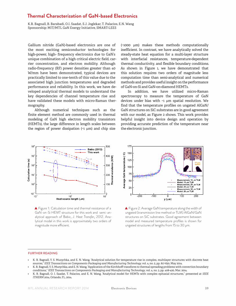
(~1000 µm) makes these methods computationally inefficient. In contrast, we have analytically solved the steady-state heat equation for a multi-layer structure with interfacial resistances, temperature-dependent thermal conductivity, and flexible boundary conditions. As shown in Figure 1, we have demonstrated that this solution requires two orders of magnitude less computation time than semi-analytical and numerical methods and provides useful insight on the performance of GaN-on-Si and GaN-on-diamond HEMTs.
In addition, we have utilized micro-Raman spectroscopy to measure the temperature of GaN devices under bias with ~1 µm spatial resolution. We find that the temperature profiles on ungated AlGaN/GaN structures on SiC substrates are in good agreement with our model, as Figure 2 shows. This work provides helpful insight into device design and operation by providing accurate prediction of the temperature near the electronic junction.
Figure 1: Calculation time and thermal resistance of a GaN-on-Si HEMT structure for this work and semi-an-alytical approach of Babic, J. Heat Transfer, 2012. Ana-lytical model in this work is approximately two orders of magnitude more efficient.
Figure 2: Average GaN temperature along the width of ungated (transmission line method or TLM) AlGaN/GaN structures on SiC substrates. Good agreement between model and measured temperature profiles is shown for ungated structures of lengths from 15 to 30 µm.
FURTHER READING
• K. R. Bagnall, Y. S. Muzychka, and E. N. Wang, “Analytical solution for temperature rise in complex, multilayer structures with discrete heat sources,” IEEE Transactions on Components Packaging and Manufacturing Technology, vol. 4, no. 5, pp. 817-830, May 2014.
• K. R. Bagnall, Y. S. Muzychka, and E. N. Wang, “Application of the Kirchhoff transform to thermal spreading problems with convection boundary conditions,” IEEE Transactions on Components Packaging and Manufacturing Technology, vol. 4, no. 3, pp. 408-420, Mar. 2014.
• K. R. Bagnall, O. I. Saadat, T. Palacios, and E. N. Wang, “Analytical model for HEMTs with complex epitaxial structures,” presented at IEEE ITHERM 2014, Orlando, FL, 2014.
40 Electronic Devices MTL ANNUAL RESEARCH REPORT 2014
A Stress/Characterization Strategy to Assess the Electrical Reliability of High-voltage GaN Field-effect Transistors S. Warnock, J.A. del Alamo Sponsorship: SRC
As the demand for more energy efficient electronics increases, GaN field-effect transistors (FETs) have emerged as promising candidates for high-voltage power management applications. Though GaN has excellent material properties, there are still many chal-lenges to overcome before GaN transistors are ready for commercial deployment. One of the concerns, for example, is a phenomenon known as current collapse or dynamic ON resistance, where the ON-resistance of the FET increases dramatically after high-voltage OFF-state biasing, due to excessive trapping. Another prob-lem that interests us is oxide reliability as a result of high voltage stress.
We are interested in contributing fundamental understanding of the physics behind the instability and reliability of high-voltage GaN FETs. Such studies require quick and accurate characterization of transistors during high stress experiments. To meet this goal, we have developed a stress-characterization suite in MATLAB to carry out a variety of stress and recovery tests. Our experimental configuration allows us to isolate DC (for stress and I-V characterization)
and AC (for C-V characterization) signals from each other, so we can apply high-voltage stress to a GaN FET, interrupt it, measure the C-V or I-V characteristics (or both) that give a picture of the degradation that may be occurring, and then resume the stress. All of this can be done automatically and without changing the cabling configuration.
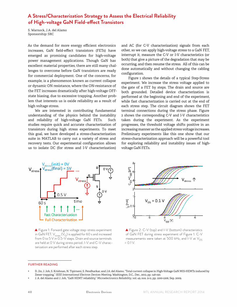
Figure 1 shows the details of a typical Step-Stress experiment. We increase the stress voltage applied to the gate of a FET by steps. The drain and source are both grounded. Detailed device characterization is performed at the beginning and end of the experiment, while fast characterization is carried out at the end of each stress step. The circuit diagram shows the FET terminal connections during the stress phase. Figure 2 shows the corresponding C-V and I-V characteristics taken during the experiment. As the experiment progresses, the threshold voltage shifts positive in an increasing manner as the applied stress voltage increases. Preliminary experiments like this one show that our stress-characterization approach will be a powerful tool for exploring reliability and instability issues of high-voltage GaN FETs.
Figure 1: Forward gate voltage step-stress experiment in GaN FET. Vstress (VG) is applied for 60 s and increased from 0 to 5 V in 0.5-V steps. Drain and source terminals are held at 0 V during stress period. I-V and C-V charac-terization are performed after each stress step.
Figure 2: C-V (top) and I-V (bottom) characteristics of GaN FET during stress experiment of Figure 1. C-V measurements were taken at 500 kHz, and I-V at VDS
= 0.1 V.
FURTHER READING
• D. Jin, J. Joh, S. Krishnan, N. Tipirneni, S. Pendharkar, and J.A. del Alamo, “Total current collapse in High-Voltage GaN MIS-HEMTs induced by Zener trapping,” IEEE International Electron Devices Meeting, Washington, D.C., Dec., 2013, pp. 148-150.
• J. A. del Alamo and J. Joh, “GaN HEMT reliability,” Microelectronics Reliability, vol. 49, nos. 9-11, pp. 1200-1206, Sep. 2009.

MTL ANNUAL RESEARCH REPORT 2014 Electronic Devices 41
Structural Degradation of GaN HEMTs under High-power and High-temperature Stress Y. Wu, J.A. del Alamo Sponsorship: Office of Naval Research DRIFT-MURI
As a result of their wide band gap energy and high break-down electric field, GaN heterostructure transistors are promising candidates for high-power and high-frequen-cy applications. However, the reliability of GaN high-elec-tron-mobility transistors (HEMTs) is still a major issue that prevents their wide deployment. Several works have shown the appearance of prominent physical damage on the semiconductor surface in the vicinity of the gate after prolonged OFF-state stress. In power amplifier ap-plications, however, the device is typically biased in the ON-state. In spite of its importance, very little research exists on the impact of prolonged high-power stress on the structural degradation of the device. This project in-vestigates the structural degradation of GaN HEMTs bi-ased in the high-power regime.
We stressed GaN transistors at high voltage and current for prolonged periods of time. In all stressed devices, we identified pits and trenches similar to those observed under OFF-state conditions. The degree of physical damage as represented by the width and depth of trenches is found to positively correlate with the overall drain current degradation. Shown in Figure
1 are AFM scans of six different devices with different levels of degradation of the maximum drain current, IDmax (defined @ VDS = 5 V, VGS = 2 V). The more the IDmax degrades, the more severe the physical damage at the gate edge. An unexpected finding is visible erosion under the entire gate of the stressed devices, which we have found directly correlates with channel resistance, RCH, degradation.
In agreement with previous studies by our group, we have found that the pit and trench formation at the gate edge is strongly thermally activated. However, the under-gate erosion is only weakly dependent on temperature. Figure 2 shows the average pit depth and under-gate erosion depth as a function of gate finger location starting from the center of the gate. Pit depth is the largest at the center of the gate finger, where the device junction is the hottest, and it decreases away from the center towards the end of the gate finger, where the temperature is lower. In contrast, under-gate erosion is weakly dependent on location. This finding strongly suggests that two different degradation mechanisms are at work.
Figure 1: AFM pictures of the delaminated surface of six devices that have been stressed under VDS = 40 V and IDQ = 100 mA/mm. From top left to bottom right pictures, overall IDmax degradation increases.
Figure 2: Distribution of pit depth along half of the gate width for the device with an overall IDmax degradation of 21.6%. Each point in the graph represents an averaged val-ue across a 5-µm scan.
FURTHER READING
• J. Joh, J. A. del Alamo, K. Langworthy, S. Xie, and T. Zheleva, “Role of stress voltage on structural degradation of GaN high electron mobility transistors,” Microelectronics Reliability, vol. 51, no. 2, Feb. 2011, pp. 201-206.
• P. Makaram, J. Joh, J. A. del Alamo, T. Palacios, and C. V. Thompson, “Evolution of structural defects associated with electrical degradation in AlGaN/GaN high electron mobility transistors,” Applied Physics Letters , vol. 96, no. 23, p. 233509, June 2010.
• L. Li, J. Joh, J. A. del Alamo, and C. V. Thompson, “Spatial distribution of structural degradation under high-power stress in AlGaN/GaN high electron mobility transistors,” Applied Physics Letters , vol. 100, p. 172109, 2012.

42 Electronic Devices MTL ANNUAL RESEARCH REPORT 2014
Threshold Voltage Instability in GaN Power Field-effect TransistorsA. Guo, J.A. del Alamo Sponsorship: NDSEG Research Fellowship
Gallium nitride (GaN) exhibits a higher electron mobili-ty and a higher bandgap than silicon. This combination endows GaN power field-effect transistors (FETs) with a very low ON resistance, fast switching frequency, and an ability to handle large voltages. This makes them a promising alternative to silicon transistors in various high-voltage switching applications including electric vehicles, DC-DC converters, and solar and wind turbine applications. At the same time, GaN power FETs suffer from reliability and stability problems, particularly un-der high-voltage operation. In this study, we address an important reliability concern, which is the stability of the threshold voltage (VT) under high-voltage stress.
To understand the impact of high voltage stress on the threshold voltage of GaN power FETs, we have developed a benign measurement scheme so that VT is not affected by the measurement itself. This is especially important for GaN devices because the significant trapping that takes place can “fog” the measurement results. We stress the device at different gate and drain voltages and examine the evolution of VT during stress. Periodically, we use a thermal step to detrap electrons and return the device to a well-defined state that we use to assess degradation. Preliminary observations show that the magnitude and direction of VT shift (ΔVT) are related to both the location (either gate or drain) and magnitude of the stress voltage. In general, |ΔVT| increases with the increase of the voltage stress. For reverse gate stress
less than 40 V and drain stress less than 90 V, the VT shift is fully recoverable, suggesting that it is entirely due to trapping.
To understand the cause of this VT instability, we have developed a technique to map the evolution of the entire transfer characteristics of a transistor after voltage stress in a time scale that starts at 5 ms. This mapping was done by tracing the drain current as a function of time at different gate biases after the stress is removed. Thermal detrapping was used to restore the device to its original state after each trace. Figure 1 shows a typical result after stressing a typical device at VGS=-20 V and VDS=0 V. A prominent negative shift in VT right occurs as a result of stress that is followed by a positive VT overshoot. Figure 2 shows this peculiar time evolution of VT more clearly. The negative VT shift right after the stress period is restored at around 10 seconds, yet VT continues to shift positive till about 100 seconds; it slowly starts to recover towards its original value. These observations suggest that the VT shift under negative gate voltage stress is the result of two competing trapping mechanisms with different impacts on the sign of ΔVT and different time constants.
Going forward, we will map out the key dependencies of this VT instability, uncover its physical origin, and provide design recommendations to minimize this problem in GaN power FETs.
Figure 1: Subthreshold characteristics at VDS= 0.1 V of GaN power MOSFET after negative VGS stress (VGS=-20 V, VDS= 0 V) for 30 s. First trace shown is taken 5 ms after stress stops. The last is taken at t= 750 s. Initial characteristics of the virgin device also appear.
Figure 2: Time evolution of VT (defined at drain current = 1 µA/mm) for experiment in Figure 1.

MTL ANNUAL RESEARCH REPORT 2014 Electronic Devices 43
Current-voltage Model for Graphene Solution-gated Field-effect TransistorsC. Mackin, A. Hsu, L. Hess, Y. Song, J. Kong, J. Garrido, T. Palacios Sponsorship: Institute for Soldier Nanotechnologies
Graphene’s chemical resilience enables a direct inter-face with many chemical and biological environments. This trait is particularly beneficial for the electrolytic environments present in a variety of biological and chemical sensing applications because graphene can exploit the electrical double layer phenomenon and resulting ultra-high interface capacitance. This large capacitance coupled with graphene’s high mobility en-ables high-transconductance and low-noise field effect transistor (FET) sensors. In addition, the recent devel-opment of chemical vapor deposition growth process-es enables graphene to span large-areas with continui-ty and consistent material properties at low cost.
A number of models have been developed to study and predict the behavior of metal-oxide-gated graphene FETs. Little work, however, has been reported for graphene solution-gated FET models. Solution-gated graphene FET models represent an increase in complexity over metal-oxide-gated graphene FETs because the top-gate capacitance cannot be considered constant. The top-gate capacitance of graphene SGFETs, which is comprised of the electrical double layer capacitance and graphene quantum capacitance, varies as a function of ionic species and concentration and also spatially along the graphene channel.
−0.2 0 0.2 0.4 0.6 0.8 1 1.20
100
200
300
VGS (V)
IDS
(µA)
Figure 1: MTL fabricated graphene solution-gated field-effect transistor.
Figure 2: Experimental (solid) and simulated (dashed) source-drain current versus VGS. VDS varies from 50 mV to 300 mV in increments of 50 mV.
FURTHER READING
• L. H. Hess, M. V. Hauf, M. Seifert, F. Speck, T. Seyller, M. Stutzmann, I. D. Sharp, and J. A. Garrido, “High-Transconductance Graphene Solution-Gated Field Effect Transistors,” Appl. Phys. Lett., vol. 99, no. 3, p. 033503, 2011.
• I. Meric, M. Y. Han, A. F. Young, B. Ozyilmaz, P. Kim, and K. L. Shepard, “Current Saturation in Zero-Bandgap, Top-Gated Graphene Field-Effect Transistors,” Nat. Nanotechnol., vol. 3, no. 11, pp. 654–9, Nov. 2008.
• J. Xia, F. Chen, J. Li, and N. Tao, “Measurement of the Quantum Capacitance of Graphene,” Nat. Nanotechnol., vol. 4, no. 8, pp. 505–9, Aug. 2009.

44 Electronic Devices MTL ANNUAL RESEARCH REPORT 2014
An Ambipolar Virtual-source-based Charge-current Compact Model for Nanoscale Graphene TransistorsS. Rakheja, D.A. Antoniadis Sponsorship: NSF NCN – NEEDS Node
The rich physical properties of graphene make it an excellent candidate for implementing a variety of high-frequency analog electronic devices. To design and simulate electronic circuits built with graphene devices, we need compact device models that include both a description static transport of carriers in the de-vice and dynamic channel-charge distribution.
This work has developed a transport model based on the concept of a virtual source for graphene field-effect transistors (GFETs) in both unipolar and ambipolar regimes of transport. The model describes the quasi-saturation in GFETs that occurs through the shift in the minimum conduction point with drain-source bias in graphene. Further, the model accounts for the asymmetry introduced in the contact resistance for electrons and holes; this asymmetry arises because of the different interfacial potential barrier heights for electrons and holes. The model has a limited number of parameters, most of which have a physical meaning and can easily be obtained from device characteriza-
tion. To describe the dynamic operation of the tran-sistor, terminal charges are obtained self-consistently with the transport formulation and can be extended to the ballistic regime, where the gradual channel approx-imation fails. The model has been extensively calibrat-ed with both DC I-V and s-parameter measurement of devices with gate lengths from 650 nm to 40 nm.
Figure 1 shows the output characteristics of devices with various gate lengths. Figure 1 shows that the model (solid lines) provides an excellent match with the experimental data (symbols) of these devic-es. Figure 2 shows the current gain versus frequency for the GFETs. Experimental data appear in symbols, while model fits appear as solid lines. The quasi-bal-listic charge model provides an excellent match to the experimental data. The model developed in the work has continuous currents and charges and can easily be used in the design and simulation of circuits and sys-tems implemented with GFETs.
Figure 1: Output curves of various graphene FETs with gate lengths from 650 nm to 40 nm with Si3N4 top-gate dielectric. Symbols represent experimental data; solid lines are obtained from the model.
Figure 2: Current gain versus frequency for GFETs. The inset of the plot shows the cut-off frequency for the 40-nm device obtained using the Gummel method. Symbols represent experi-mental measurements; solid lines are model fits.
FURTHER READING
• H. Wang, A. Hsu, J. Wu, J. Kong, and T. Palacios, “Graphene-based ambipolar RF-mixers,” IEEE Electron Device Letters, vol. 31, no. 9, pp. 906-908, 2010.
• S. Rakheja, H. Wang, T. Palacios, I. Meric, K. Shepard, and D. A. Antoniadis, “A unified charge-current compact model for ambipolar operation in quasi-ballistic graphene transistors: experimental verification and circuit analysis demonstration,” Electron Devices Meeting, 2013 IEEE International, pp. 5.5.1-4, Dec. 2013.
• Y. Wu, K. A. Jenkins, A. Valdes-Garcia, D. B. Farmer, Y. Zhu, A. A. Bol, C. Dimitrakopoulos, W. Zhu, et al., “State-of-the-Art Graphene High-Frequency Electronics,” Nano Letters, vol. 12, no. 6, pp. 3062-3067, June 2012.

MTL ANNUAL RESEARCH REPORT 2014 Electronic Devices 45
Graphene-MoS2 Hybrid Technology for Large-scale Two-dimensional ElectronicsL. Yu, H. Wang, Y. Lee, X. Ling, Y. Shin, J. Kong, T. Palacios Sponsorship: Office of Naval Research Young Investigator Program, Office of Naval Research GATE-MURI, Army Research Laboratory
Two-dimensional (2D) materials have generated great interest in the last few years as a new set of tools for electronics, for these materials can push electronics beyond its traditional boundaries. This family of ma-terials includes metallic graphene, semiconducting transition metal dichalcogenides (such as MoS2) and insulating boron nitride. These materials and their het-erostructures offer excellent mechanical flexibility, op-tical transparency, and favorable transport properties for realizing electronic, sensing, and optical systems on arbitrary surfaces. To harvest the full advantages of 2D electronics in bendable electronics, constructing systems solely based on 2D materials and their hetero-structures is highly desirable.
We use a novel technology to construct large-scale electronic systems based on graphene/molybdenum disulfide (MoS2) heterostructures grown by chemical vapor growth. The atomically thin heterostructure is realized by using ALD Al2O3 as an etch-stop layer. This Al2O3 layer also acts as the top gate dielectric for the
devices. High-performance devices and circuits based on this heterostructure with MoS2 as transistor channel, graphene as contact electrodes and circuit interconnects have been fabricated, as shown in Figure 1. The systematic comparison between graphene/MoS2 and Ti/MoS2 devices shows that the use of graphene as contacts for MoS2 FETs, as discussed above, provides 10 times lower contact resistance, 10 times higher on-current and field effect mobility than conventional MoS2-metal contacts (Figure 2a,b). The Schottky barrier height of graphene/MoS2 and Ti/MoS2 device are extracted through low temperature measurement. The work function of graphene is strongly tuned by the back gate voltage and this unique property significantly improves ohmic contact to MoS2. Top gated devices are also fabricated and measured. Based on this technology, basic logic integrated circuits are also demonstrated (Figure 2c,d). This technology represents the first scalable platform for constructing large scale electronics on Van der Waals’ heterostructures based on 2D material monolayers.
Figure 1: (a) Optical micrograph of large-scale chip of MoS2 devices and circuits using CVD graphene as electrodes and interconnects (white dashed box) and controlled devices and circuits using Ti/Au electrodes in adjacent (red dashed box). Metal pads (gold color) are fabricated on the sample for convenient measurement. (scale bar: 200µm).
Figure 2: (a) MoS2-graphene (MoS2-G) and (b) MoS2-Ti FETs back-gate transfer performance at room temperature. Current density in left axis and transcon-ductance in right axis. (c),(d) Demonstration of an in-tegrated logic inverter on MoS2-G heterostructure. (c) Output curve for MoS2-G logic inverter. Optical image (inset, left down) and schematic of electronic circuit (in-set, right up) for inverter. (d) Gain of inverter is >12.
FURTHER READING
• H. Wang, L. Yu, Y.-H. Lee, Y. Shi, A. Hsu, M. L. Chin, L.-J. Li, M. Dubey, J. Kong, and T. Palacios, “Integrated Circuits Based on Bilayer MoS2 Transistors,” Nano Lett., vol. 12, no. 9, pp. 4674–4680, Sep. 2012.
• Y.-H. Lee, L. Yu, H. Wang, W. Fang, X. Ling, Y. Shi, C.-T. Lin, J.-K. Huang, M.-T. Chang, C.-S. Chang, M. Dresselhaus, T. Palacios, L.-J. Li, and J. Kong, “Synthesis and Transfer of Single-Layer Transition Metal Disulfides on Diverse Surfaces,” Nano Lett., vol. 13, no. 4, pp. 1852–1857, Apr. 2013.

46 Electronic Devices MTL ANNUAL RESEARCH REPORT 2014
High-performance WSe2 CMOS Devices and Integrated CircuitsL. Yu, A. Zubair, T. Palacios Sponsorship: NSF CIQM, Army Research Laboratory, Office of Naval Research
Two-dimensional (2D) crystals have outstanding prop-erties for developing the next generation of electronic devices because of the excellent electrostatic control of the channel associated with their atomically thin struc-ture. For many of these applications, the realization of complementary metal-oxide-semiconductor (CMOS) logic is crucial to get high performance integrated cir-cuits. CMOS logic has high noise immunity, low static power consumption, and high density of integration. So far, complementary logic circuits have been demon-strated only on heterostructures of different layered materials with gain less than 2 and zero noise margins. In this work, we demonstrate both pMOS and nMOS technologies on exfoliated WSe2, and we use them to fabricate monolithic CMOS integrated logic inverters with rail-to-rail logic operation, small power dissipa-tion, large noise margin, and voltage gain.
Figure 1 (right) shows the fabrication process for our WSe2 CMOS technology. The gate metal and dielectric stack were deposited before the WSe2 layer and annealed to remove the negative charge inside the dielectric layer. Then exfoliated WSe2 flakes were transferred on top of the gate region. A low work function metal (i.e., silver) and a high work function metal (i.e., Pd) were used to contact nMOS and pMOS FET, respectively. After source-
drain contact, the nMOS FET shows strong n-type and good ohmic performance, while the pMOS FET shows weak n-type and barely p-type performance and a large Schottky barrier at the contact region. After locally doping the p-type channel, we achieved strong p-type performance and good ohmic contacts. Figures 2 a and b show the transfer characteristics of WSe2 nMOS and pMOS FETs, respectively. They both show current on/off ratio larger than 105 and pinch-off current saturation. The field effect mobility for electron and hole are 5 and 13 cm2/V.s. respectively. The figures show very symmetric threshold voltage and balanced on-current, which is crucial to get a large noise margin and gain in CMOS inverters. The optical image and output performance of an integrated CMOS inverter are shown in Figure 1 and Figures 2 c and d, respectively. With a Vdd of 6V, the threshold for inverting behavior happens at Vin=3V with rail-to-rail logic performance (Vhigh=Vdd and Vlow =0V), providing an excellent noise margin, as shown in Figure 1c. The inverter gain is larger than 30 (see Figure 1d), and the switching power is 120nW per cycle. This high performance logic inverter demonstrates the large promise of WSe2 for the next generation of CMOS technology.
Figure 1: Schematic (left, top), optical image (left, bottom) and fabrication process (right) for WSe2 CMOS FET technology.
Figure 2: Transfer characteristics of nMOS (a) and pMOS (b) WSe2 FETs. (c) Output characteristics of CMOS logic inverter. (d) Inverter Gain and current during operation.
FURTHER READING
• H. Wang, L. Yu, Y.-H. Lee, Y. Shi, A. Hsu, M. L. Chin, L.-J. Li, M. Dubey, J. Kong, and T. Palacios, “Integrated Circuits Based on Bilayer MoS2 Transistors,” Nano Lett., vol. 12, no. 9, pp. 4674–4680, Sep. 2012.