electronic and optical properties of silicon nanocrystals
TRANSCRIPT

Electronic and Optical Properties
of Silicon Nanocrystals:
a Tight Binding Study
Fabio Trani
November 30, 2004

2

Contents
Introduction 5
1 Tight Binding method 9
1.1 Introduction . . . . . . . . . . . . . . . . . . . . . . . . . . . . 9
1.2 The model . . . . . . . . . . . . . . . . . . . . . . . . . . . . . 11
1.3 Empirical pseudopotentials . . . . . . . . . . . . . . . . . . . . 16
1.4 Parametrizations . . . . . . . . . . . . . . . . . . . . . . . . . 19
2 Linear Response Theory 29
2.1 Introduction . . . . . . . . . . . . . . . . . . . . . . . . . . . . 29
2.2 Response of a crystal to an external field . . . . . . . . . . . . 30
2.3 Interaction picture and correlation functions . . . . . . . . . . 34
2.4 The dielectric tensor . . . . . . . . . . . . . . . . . . . . . . . 37
2.5 Linear response and TB . . . . . . . . . . . . . . . . . . . . . 42
2.6 The approximation . . . . . . . . . . . . . . . . . . . . . . . . 45
2.7 The charge conservation . . . . . . . . . . . . . . . . . . . . . 47
2.8 Results . . . . . . . . . . . . . . . . . . . . . . . . . . . . . . . 50
3 Spherical nanocrystals 55
3.1 Introduction . . . . . . . . . . . . . . . . . . . . . . . . . . . . 55
3

4 CONTENTS
3.2 The method . . . . . . . . . . . . . . . . . . . . . . . . . . . . 56
3.3 Energy levels . . . . . . . . . . . . . . . . . . . . . . . . . . . 59
3.4 Dielectric function . . . . . . . . . . . . . . . . . . . . . . . . 63
3.5 Oscillator strengths . . . . . . . . . . . . . . . . . . . . . . . . 67
3.6 k-space projections . . . . . . . . . . . . . . . . . . . . . . . . 69
3.7 Dielectric constant . . . . . . . . . . . . . . . . . . . . . . . . 72
4 Ellipsoidal nanocrystals 75
4.1 Introduction . . . . . . . . . . . . . . . . . . . . . . . . . . . . 75
4.2 Porous Silicon Photoluminescence . . . . . . . . . . . . . . . . 76
4.3 Silicon ellipsoids . . . . . . . . . . . . . . . . . . . . . . . . . . 78
4.4 Dielectric properties . . . . . . . . . . . . . . . . . . . . . . . 82
4.5 Energy levels of large ellipsoids . . . . . . . . . . . . . . . . . 89
Conclusions 99
A Symmetries 103
B Character Tables 107
Acknowledgments 111
Bibliography 120

Introduction
The scientific field of silicon nanostructures is a fascinating area of material
science. It has a huge technological impact, because of the fundamental role
of silicon in the microelectronic revolution which has changed our everyday
lives. On the other side, silicon is a very bad luminescent material. It is char-
acterized by an indirect, low energy fundamental band gap. And this means
that silicon shows very long radiative electron-hole recombination lifetimes,
so that non-radiative recombination paths are preferred, even at cryogenic
temperatures. In the past years, it became clear that silicon nanocrystals
behave in a completely different way. The chance of tuning the optical band
gap and the radiative recombination lifetime with the nanocrystal size is
known as the quantum confinement effect, and is a simple consequence of
the quantum mechanics rules. Nevertheless, the construction in labs all over
the world of nanocrystals with a strong photoluminescence in the entire op-
tical range, have astonished the whole community of solid state scientists.
The research of the last decade has been devoted to the attempts of having
light-emitting silicon devices. Using both the lithographic-epitaxial and the
chemical synthesis techniques, the fabrication of silicon nanocrystals have had
an enormous progress in the last years, and sharper and sharper nanocrystal
size distributions have been obtained. An important goal was the discovery
5

6 INTRODUCTION
of a strong photoluminescence from porous silicon, which constituted a very
easy and economic way for having high-performance photoluminescent silicon
structures. Recently, the discovery of optical gain from silicon nanocrystals
have suggested the possibility of a silicon-based laser technology.
From the theoretical point of view, still today the subject is not com-
pletely clear. While the quantum confinement effect has been recognized as
the major cause of the photoluminescence, many doubts remain on the way
in which the phenomenon takes place. This thesis is the result of a deep
work in the understanding of the optical properties of silicon nanocrystals.
The first part of the thesis is dedicated to the making-up of the theoretical
model. The first chapter concerns the Tight Binding method, used in this
work for the study of the nanocrystals. The advantages in the use of such
a method lies in its huge efficiency: Tight Binding is the only method able
to study both small and very large nanocrystals. In fact, its short range
interaction parameters lead to nanocrystal Hamiltonian matrices really very
sparse. This feature has been used through a diagonalization routine having
a computational time which scales linearly with the matrix size. The second
chapter is dedicated to a review of the linear response theory, and to the ex-
tension of the Tight Binding method to the study of the dielectric properties
of a crystalline structure. This is not a trivial matter, in that the method
does not easily allow an explicit knowledge of the basis wave functions. The
method that we have chosen seems to work very well for the Bulk Silicon.
The second part of this thesis is dedicated to the results. In the third chapter,
the optical properties of spherical nanocrystals are illustrated. A comparison
with the experimental results and the other calculation tools are discussed

INTRODUCTION 7
in detail. The optical gap, the imaginary part of the dielectric function, the
static dielectric function, and the radiative electron-hole recombination times
have been calculated. An interesting feature is the existence of an energy gap
between the energy of the first transition and the threshold of the absorption
cross section. This is an indication that the electronic features of the bulk
silicon are always reflected into the silicon nanocrystal physics. A very nice
confirmation of this trend is the k-space projection of the nanocrystal states,
which gives a fair explanation of this phenomenon. In the last chapter the
shape effects on the optical properties are shown. Several sets of ellipsoidal
nanocrystals, with different sizes and shapes, have been analyzed, and the ef-
fects of the geometrical anisotropy on the polarization of the dielectric tensor
is discussed.

8 INTRODUCTION
Chapter 1
Tight Binding method
1.1 Introduction
Since the fundamental paper of Slater and Koster (SK) [1], the Tight Binding
interpolation scheme (TB) has been a powerful tool for electronic spectra
and density of states calculations of crystalline structures. The method is
based on the expansion of the wave functions into linear combinations of
atomic orbitals (LCAO), with Hamiltonian matrix elements parametrized
in such a way to reproduce first-principles calculations and/or experimental
data. Compared to the methods based on the Plane Wave basis sets (PW),
the TB scheme is very efficient in problems where localized functions are
required. In fact, the method has been widely used especially in impurity
states calculations [2], where it is computationally advantageous because it
only needs a small number of localized orbitals. Over the years, many variants
of the TB have been developed, based on different kinds of parametrizations,
and the possibilities of the method have been extended beyond the simple
band structure calculations [3]. An interesting field has concerned the study
9

10 TIGHT BINDING METHOD
of the TB parameters transferability [4], that allows the method to be used
in structural optimization problems. Nowadays, total energy calculations
and Monte Carlo simulations [5, 6] are currently performed within the TB
formalism.
With the increasing of computer performances, ab initio TB models have
been attracting a great interest. In fact, the TB interpolation schemes are
empirical tools, often called Empirical Tight Binding, in which we usually do
not have an explicit knowledge of neither the basis functions, nor the real
space Hamiltonian. On the other hand, the ab initio approaches are based
on the explicit construction of both the localized atomic orbitals and the
Hamiltonian matrix elements. The ab-initio TB models can be very accurate
and powerful, but they are computationally more demanding. Therefore, for
the great simplicity of the original SK formulation, and the huge precision
reached in getting accurate band structures, the Empirical TB models are
still today very attractive calculation tools.
In this chapter, we discuss the ETB scheme as it is usually used in band
structure calculations. As a first step, in the next section the method will
be illustrated, according to the usual Slater-Koster scheme. Then, a brief
description of the Empirical Pseudopotential method (PP), often used as an
important comparison scheme, will be given, trying to explain the reasons for
its great efficiency for the bulk structures, and the huge computational effort
that it requires for the nanocrystals. After this, we will compare several TB
parametrizations available in literature for the crystalline silicon, the material
of major interest in this thesis. Finally, a comparison with the experimental
data of gap energies and effective masses will be shown.

1.2. THE MODEL 11
1.2 The model
The starting point of every Tight Binding model is the definition of a suit-
able set of atomic-like orbitals. In the following we shall only consider bulk
crystalline structures, with atoms located in the positions of a Bravais lattice
with a basis; we indicate with R the lattice vectors, and µ the atomic posi-
tions within the unit cell. Therefore, all the atoms contained in the structure
lie in the positions:
Rµ ≡ R + µ. (1.1)
In the case of the bulk silicon (diamond structure), the Bravais lattice is an
FCC and there are two atoms in the unit cell, whose positions are:
µ = 0,d, (1.2)
where d = a4(1, 1, 1)1, and a is the lattice length.
The TB orbitals are localized at the atomic positions, and they are usu-
ally chosen in such a way to transform into each other under the crystal point
group operations, according to a suitable irreducible representation (see Ap-
pendix (A) for more details on symmetries). Each orbital is characterized
by a quantum number σ, which labels its transformation properties. We use
the Dirac notation to represent orbitals, so we write
|σµR〉 (1.3)
to label an orbital centered at the atomic position R + µ, having σ symme-
try. A possible basis set for the study of a bulk structure is obtained from
the orbitals of the isolated, non interacting atoms. This choice leads to a
1 We are using the standard, cubic coordinate system.

12 TIGHT BINDING METHOD
TB model, which is based on functions having the full rotational symmetry2,
which are symmetric by inversion, and where σ labels the quantum numbers
of the single atom states (nlmms). In the case of the silicon, which is a crys-
tal with a single atomic species, this method allows us to choose the basis set
so that all the crystal orbitals are obtained by translations of those orbitals
located in the coordinate origin. This simple method is very nice in that
the basis orbitals have the symmetry of the whole rotation group (they are
eigenstates of the atomic angular momentum operators). On the other side,
it has the disadvantage that the basis functions are not orthogonal. For this
reason, at least two kinds of parameters must be used: Hamiltonian matrix
elements and overlap parameters. The difficulty of this non-orthogonal TB
scheme [1] is in the large number of parameters that enter the fitting pro-
cedure, so that it is difficult to include interactions up to many neighbors
without doing suitable approximations [7]. Another complication arises from
the fact that the energy levels are solutions of a generalized eigenvalue prob-
lem. This is not a big problem in crystalline structures, where we always
have a small number of orbitals in the unit cell. But this can give troubles in
nanostructures, by increasing the computational time, when the Hamiltonian
matrices become very large.
The use of an orthogonal basis set simplifies both the fitting and the
Hamiltonian diagonalization procedures. Starting from a non-orthogonal ba-
sis set, a smart orthogonalization procedure can be performed, as it was
shown by Lowdin [8], in such a way that the resulting orbitals maintain
the same transformation properties of the original basis set under the space
2 Of course, only in the hypothesis of neglecting the small non central corrections tothe isolated atom Hamiltonian, the angular momentum is a good quantum number, andwe can choose atomic functions with the full rotational symmetry.

1.2. THE MODEL 13
group operations [1]. The as-built Lowdin’s orbitals usually have a lower
symmetry than the original functions. If we start from a set of eigenstates
of the angular momentum operators of the isolated atoms, after the orthog-
onalization procedure we obtain a new set of orbitals which are symmetric
only with respect to those (discrete) rotations which transform the crystal
atoms into each other. And so, we eventually retrieve a basis set which is not
symmetric with respect to the full rotational group. Moreover, if the point
group is not symmorphic [9] (there are transformations associated to frac-
tional translations, see Appendix (A)), there are couples of orbitals which
belong to different sublattices that can be no longer related to each other
through a simple spatial translation. In effect, this is the situation for the
bulk silicon, where Lowdin’s orbitals do not have the inversion symmetry,
since the inversion is related to a fractional translation (when the origin has
been taken on a silicon atom). The inversion operation plus the fractional
translation transforms into each other the orbitals which belong to different
sublattices.
In the Orthogonal TB model, the basis set is constituted by Lowdin’s
orbitals, and we have:
〈σµR|σ′µ
′R′〉 = δσσ′δµµ′δRR′ . (1.4)
The only parameters we need for electronic spectra calculations are the
Hamiltonian matrix elements, that we label as
Hµµ′
σσ′ (R′µ′ − Rµ) ≡
⟨
σµR
∣
∣
∣H
∣
∣
∣σ′
µ′R′
⟩
. (1.5)
As usual in the study of the crystalline structures, we construct a basis set
of Bloch sums, in order to take into account the translational symmetry of

14 TIGHT BINDING METHOD
the lattice. In our scheme we obtain the following orthogonal states:
|σµk〉 =1√N
∑
R
eik·(R+µ) |σµR〉 , (1.6)
in which N is the number of lattice sites included into the sum. These func-
tions are invariant (up to a phase factor) by lattice translations, and therefore
they form a basis set in which the Hamiltonian operator H is diagonal with
respect to k. The Hamiltonian matrix in this new basis set is easily computed
starting from the interaction parameters defined in Eq. (1.5) :
Hµµ′
σσ′ (k) ≡ 〈σµk |H|σ′µ
′k〉 =∑
R
eik·(R+µ′−µ) 〈σµ0 |H|σ′µ
′R〉 (1.7)
The band structure is now obtained solving the eigenvalue problem for the
reciprocal space Hamiltonian matrix of Eq. (1.7), for each k-vector lying
inside the first Brillouin Zone (BZ):
∑
σ′µ′
[
Hµµ′
σσ′ (k) − En(k)δσσ′δµµ′
]
Bµ′
σ′n(k) = 0, (1.8)
and the crystalline eigenstates come from the expansion
|nk〉 =∑
σµ
Bµσn(k) |σµk〉 . (1.9)
The above procedure only requires the knowledge of the interaction parame-
ters (1.5) in order to calculate the single-electron energy levels of bulk struc-
tures. Using symmetries, all these parameters can be reduced to a minimum
number. As we shall see later, two factors enter into the definition of a
TB scheme: the number of species of atomic orbitals (the values that σ can
assume), and the number of nearest neighbors that interact with a single
orbital. These two factors determine the number of independent parame-
ters. By the analysis of the crystal, physical reasons can lead to prefer a, we

1.2. THE MODEL 15
can say, horizontal enlargement, using a small basis set, and interactions up
to many neighbors, or a vertical enlargement, using a few neighbors but a
greater basis set.
Based on a physical ground, approximations can be done in order to
reduce the number of parameters. A widely used one is the so called two-
center approximation [1], that can significantly reduce the number of parame-
ters [10]. The approximation consists in considering the potential energy3 in-
variant by rotations with respect to the axis connecting the two atoms where
the orbitals are located. The problem, in these terms, greatly simplifies, es-
pecially for far enough orbitals, in that a number of terms are automatically
put equal to zero. The used labelling is that of the diatomic molecule spectra,
and all the parameters are reduced to only σ, π . . . interactions. In effect, this
approximation consists in retaining only that part of the crystalline potential
energy which is located in the neighborhood of the two orbitals, and neglect-
ing all the remaining terms (the so-called three center integrals). Some care
should be taken in using this approximation, which often can be too rough
for a quantitative study of crystals.
After that a suitable set of independent interaction parameters has been
chosen, the next step of the Empirical TB scheme is based on calculating
them in such a way to fit, after the diagonalization of Eq. (1.8), experimen-
tal data and/or ab initio calculation results of energy gaps and/or effective
masses, in high symmetry k-points.
3 The potential energy enters the interaction parameters in Eq. (1.5). The two centerapproximation leads to a simplification of the problem, with the reduction of the totalnumber of parameters.

16 TIGHT BINDING METHOD
1.3 Empirical pseudopotentials
In this section we want to spend a few words on the empirical pseudopotential
scheme, that we often use as a comparative computational tool, in order to
address the precision of the Tight Binding method. The scheme is based on
the expansion of the crystalline eigenstates into Plane Waves, organized in
such a way to take into account the translational symmetry of the lattice:
|nk〉 =∑
G
Ank (G) |k + G〉 . (1.10)
Here, the sum is done on all the reciprocal lattice vectors G, and Plane Waves
are defined in real space as:
〈r|k + G〉 ≡ 1√V
eı(k+G)·r, (1.11)
where they have been normalized to the crystal volume V . In the local
formulation of the method, the crystalline potential is written as the sum of
atomic spherically symmetric contributions v(r), so that the single-electron
Hamiltonian for silicon is written as:
H =p2
2m+
∑
µ,R
v (|r − R− µ|) . (1.12)
The method is very simple, and the Hamiltonian matrix elements are
⟨
k + G
∣
∣
∣H
∣
∣
∣k + G′
⟩
=h2
2m|k + G|2 δG,G′ + V (G − G′) , (1.13)
where for silicon4 we have:
V (G) = v(G)∑
µ
e−ıG·µ = v(G)(
1 + e−ıG·d)
. (1.14)
4 Where we use the atomic positions that we have defined in the previous section.

1.3. EMPIRICAL PSEUDOPOTENTIALS 17
Here v(G) is the Fourier transform of the atomic potential. The use of
the pseudopotential method as an empirical interpolation scheme consists
in using v(G) as unknown parameters, and fit them in such a way to have
a good agreement with the experimental data. The eigenvalue problem is
written as:
∑
G
[(
h2
2m|k + G|2 − En (k)
)
δG,G′ + V (G − G′)
]
An,k(G) = 0, (1.15)
and is characterized by a great simplicity of calculation of the matrix ele-
ments. The feasibility of this method is based on how many parameters are
needed in order to reproduce a good band structure, as well as on the number
of Plane Waves needed to reach the convergence.
The answer was given already many years ago, when it was shown that
very few parameters and a not too large basis set succeeded in getting a
quite good agreement with the experimental data, for a huge class of semi-
conductors [11, 12]. The physical motivations of this very nice behavior lie
in the idea which is behind a pseudopotential [13]. In semiconductors, the
whole space can be divided into a core region, quite close to the ions, and an
interstitial region, constituted by the space between ions. We expect that
the lower energy electrons (the so called core electrons), are mainly localized
in the core region, while the higher energy electrons (the valence electrons)
lie in the interstitial region. It is easy to realize that these latter electrons
determines the band structures near the Fermi level, and therefore the opti-
cal properties of the crystal.
The explicit form of the potential inside the core region is not impor-
tant in studying the optical properties, and we can use a fictitious potential
(the pseudopotential) which is smoother than the real potential in the core

18 TIGHT BINDING METHOD
region, and equal to this one in the interstitial region. It has been widely
demonstrated (in many different forms) that such pseudopotentials lead to
the same optical properties of the real crystal, but, being very smooth in
the core region, they have Fourier transforms v(G) which rapidly go to zero.
Within the Empirical Pseudopotential Method (EPM), in the form it was
first proposed [11,12], an excellent band structure of bulk silicon is obtained
with only three independent parameters. It has been shown that this pa-
rameter set is indeed the best choice for taking into account in an effective
way all the higher G contributions [14,15]. Moreover, it has been shown that
EPM form factors can be calculated starting from an ab initio LDA screened
pseudopotential [16]. This theoretical ground is the best reason for using the
EPM as a comparative tool.
The method is very nice, elegant and very simple to implement. It does
not require a great computational effort for bulk crystals and, more impor-
tantly, the convergence with respect to the basis set size is under control.
We want to point out that this is a great advantage over the TB models.
In fact, within a Pseudopotential method the convergence is obtained in a
very simple way, by including into the basis set as many Plane Waves as we
need. On the contrary, enlarging a TB basis set is not an easy task, and it
is closely related to the parametrization, the number of parameters rapidly
increasing with the number of basis functions (the only inclusion of the d
orbitals requires an huge effort).
Unfortunately, the EPM, although very attracting for studying bulk crys-
tals, gives rise to some difficulties when applied to nanostructures [16]. The
usual way to study a finite structure within a plane waves approach is that

1.4. PARAMETRIZATIONS 19
of building a fictitious periodic system, by placing infinite replicas of the
original structure on the sites of a Bravais lattice, and therefore keeping us-
ing k as a good quantum number. The structure that we want to study
constitutes the unit cell (the supercell) of such a fictitious crystal, and the
problem is equivalent to the isolated structure problem in the limit of choos-
ing a lattice constant large enough to avoid any interaction between the
replicas. The great computational difficulty raises from the necessity of leav-
ing very much vacuum space between two replicas, having indeed very large
lattice constants. In order to simulate the annihilation of the nanocrystal
wavefunctions inside the vacuum zone, a great number of short-wavelength
plane waves must be included into the basis set. On increasing the size of
the structure, the supercell size increases, and so the Hamiltonian matrix
size. With standard techniques, PW methods can hardly afford the study of
nanostructures with more than a few hundreds of atoms. The TB methods,
on the contrary, in a natural way take into account the vacuum zone outside
the structure. The size of the TB basis set is linear in N , and this allows to
study structures with thousands of atoms with a low computational effort.
1.4 Parametrizations
In this section we discuss different kinds of parametrizations currently used
in the TB interpolation schemes. We only consider the case of bulk silicon,
namely crystals with the diamond structure. The different parametrizations
are characterized by the choice of both the basis set, formed by atomic or-
bitals up to a maximum quantum numbers σ, and the number of neighbors
taken into account in the Hamiltonian matrix. These two factors determine
20 TIGHT BINDING METHOD
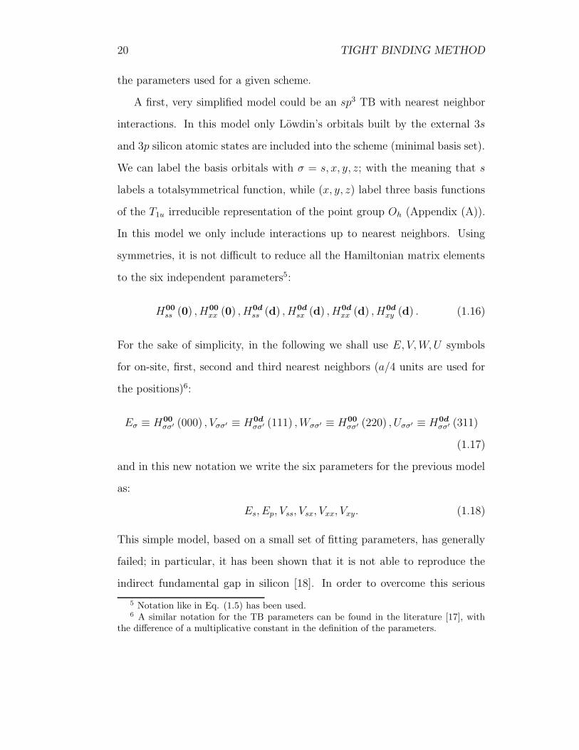
the parameters used for a given scheme.
A first, very simplified model could be an sp3 TB with nearest neighbor
interactions. In this model only Lowdin’s orbitals built by the external 3s
and 3p silicon atomic states are included into the scheme (minimal basis set).
We can label the basis orbitals with σ = s, x, y, z; with the meaning that s
labels a totalsymmetrical function, while (x, y, z) label three basis functions
of the T1u irreducible representation of the point group Oh (Appendix (A)).
In this model we only include interactions up to nearest neighbors. Using
symmetries, it is not difficult to reduce all the Hamiltonian matrix elements
to the six independent parameters5:
H00ss (0) , H00
xx (0) , H0dss (d) , H0d
sx (d) , H0dxx (d) , H0d
xy (d) . (1.16)
For the sake of simplicity, in the following we shall use E, V, W, U symbols
for on-site, first, second and third nearest neighbors (a/4 units are used for
the positions)6:
Eσ ≡ H00σσ′ (000) , Vσσ′ ≡ H0d
σσ′ (111) , Wσσ′ ≡ H00σσ′ (220) , Uσσ′ ≡ H0d
σσ′ (311)
(1.17)
and in this new notation we write the six parameters for the previous model
as:
Es, Ep, Vss, Vsx, Vxx, Vxy. (1.18)
This simple model, based on a small set of fitting parameters, has generally
failed; in particular, it has been shown that it is not able to reproduce the
indirect fundamental gap in silicon [18]. In order to overcome this serious
5 Notation like in Eq. (1.5) has been used.6 A similar notation for the TB parameters can be found in the literature [17], with
the difference of a multiplicative constant in the definition of the parameters.

1.4. PARAMETRIZATIONS 21
problem, Vogl [18] proposed an enlargement of the Lowdin’s orbital basis
set, including an excited s state (the so called s∗ state), for each atom.
This nearest neighbor sp3s∗ model requires a greater number of independent
parameters than the previous one, and between all the parameters Vogl, on
a physical ground, only retained the following:
Es, Ep, Es∗, Vss, Vsx, Vxx, Vxy, Vs∗x. (1.19)
Based on this larger set of fitting parameters, this model for silicon has been
shown to correctly describe not only the energy levels at the Γ point, but the
lowest indirect energy gap, and the first conduction band at ∆ (Γ − X) and
Λ (Γ−L) lines. On the other side, the behavior of the bands in the proximity
of the X points in directions different from ∆, such as the Z (X − W ) line,
is not good. The largest disagreement is obtained close to the W point, and
along the Σ (Γ−K) symmetry line. All these discrepancies likely arise from
the truncation of the interaction at a very low order of neighbors. We are
motivated in thinking that a first neighbor model cannot fair reproduce the
band structure in the whole first Brillouin Zone.
The overall behavior of the energy levels is well described by the density of
states (DOS). In figure (1.1) the bulk silicon band structure and DOS have
been shown, computed both with Vogl model [18] and a Pseudopotential
method. All the above considerations can be noticed; in particular it is
worth noting that the TB density of states is close to the pseudopotential
curve only for the highest energy valence bands. For the unoccupied states,
instead, the TB model largely overestimates the pseudopotential density of
states. The Vogl model still today is largely used, whereas, as we have just
shown, it should be used with care.

22 TIGHT BINDING METHOD
Before going ahead, we want to spend a few words on the density of
states. For a generic system with Ns single-electron states, each one having
an energy Ei, we define the density of states at energy E as7:
g(E) =1
Ns
∑
i
δ(E − Ei). (1.20)
In the case of a bulk crystal, the sum is done on all the Nk vectors which
lie inside the first Brillouin Zone, and all the band complex, getting the final
formula:
g(E) =1
8Nk
∑
n,k
δ(E − En(k)). (1.21)
In order to compute the DOS, a grid in the first Brillouin Zone has to be
constructed, dense enough to guarantee the convergence of the sum. The sim-
plest way to build the grid consists in choosing periodic boundary conditions
for the crystal surface, like the largely used Born-von Karman conditions. In
this case, each primitive translation vector ai (i = 1, 2, 3) is replied N times,
and one chooses the k vectors according to the conditions:
eıNk·ai = 1. (1.22)
Using values of N larger and larger, the sum finally converges to its end
value. However, there are much better ways to perform such an integration
procedure. Over the years, very smart grids have been invented, constituted
by special points of the Brillouin zone, chosen in such a way that the sum
rapidly reaches the convergence on increasing Nk. A very efficient grid is
7 Actually, we here define the density of states for each state. It is normalized to theunity, when the integration on all the energy range is considered. The current definitiondiffers in a multiplicative factor from the usual definition of density of states for unitvolume.

1.4. PARAMETRIZATIONS 23
Figure 1.1: Bulk silicon band structure (left) and density of states (right) calcu-
lated with the Vogl sp3s∗ nearest neighbor model [18] (magenta lines), compared
to a local empirical pseudopotential calculation (green lines), performed with the
parameters of Ref. [12].
obtained with the Monkhorst and Pack scheme [19], that we have used to-
gether with the Born-von Karman grid to perform integrations over the first
Brillouin zone.
In the recent years, computer performances have incredibly improved,
allowing more complex fitting procedures than in the past. In this way, fit-
ting of a band structure with many independent parameters is now possible,
with the result of making TB band structures very close to ab initio results.
Even if the first neighbor sp3s∗ TB is nowadays very used [20–25], because of
its simplicity in considering only nearest neighbor interactions, better results
are obtained using the minimal basis set sp3 and increasing the number of

24 TIGHT BINDING METHOD
-10
-5
0
5
10
-10
-5
0
5
10--- TB niquet --- TB tserbak --- EPM locale CC
Γ X W L Γ K X
Figure 1.2: Bulk silicon band structure. Blue and red lines refer to, respectively,
Niquet [28] and Tserbak [27] TB model; green lines come from a Pseudopotential
calculation, with the Chelikowsky and Cohen parameters [12].
neighbors interacting with a single orbital.
The 3rd nearest neighbor sp3 TB model is based on 20 independent pa-
rameters [26]. Tserbak et al. [27] found an optimum fit for these parame-
ters, comparing the main band gaps computed with TB and pseudopotential
method. Tserbak parameters lead to a band structure and a density of states
that are indeed accurate over the whole first Brillouin Zone, not only at the
lowest energies, in the valence band energy range, but also at the highest
energies. In fact, the first conduction band agrees well to the pseudopoten-
tial curve over the most main symmetry lines. In figure (1.2) we report
the bulk silicon band structure calculated with the pseudopotential method
and the Tserbak model. We also show the band structure from the Niquet

1.4. PARAMETRIZATIONS 25
Figure 1.3: Bulk Silicon Density of States. Red and blue lines refer, respectively,
to the Tserbak [27] and Niquet [28] TB parametrization; green line comes out from
a pseudopotential calculation [12].
parametrizations, that we are going to discuss in the following.
The Tserbak model fails just on predicting very precisely the effective
masses near the highest symmetry k-points. Especially when dealing with
nanostructures, it is desirable that, in the limit of very large systems, the
TB results merge with those coming from the Effective Mass Approximation
(EMA) theory. For this reason, very precise values of the effective masses
are required. Niquet et al. [28], starting from the Tserbak model, proposed a
new set of parameters, obtained imposing the further condition that the main
electron and hole calculated effective masses were equal to their experimen-
tal values. This new set of parameters leads to an overall less accurate band
structure than that one of Tserbak, but they give good values of the hole and
the electron effective masses. A comparison between the two parametriza-

26 TIGHT BINDING METHOD
Parameter Tserbak Niquet Parameter Tserbak Niquet
Es -6.3193 -6.17334 Wxy -0.0378 -0.05462
Ep 2.2494 2.39585 Wxz 0.0829 0.12754
Vss -1.8376 -1.78516 Wzz -0.2646 -0.24379
Vsx 1.0087 0.78088 Uss -0.0674 -0.06857
Vxx 0.3209 0.35657 Usx 0.2717 0.25209
Vxy 1.4889 1.47649 Usy -0.1262 -0.17098
Wss 0.1940 0.23010 Uxx 0.0869 0.13968
Wsx -0.1840 -0.21608 Uxy 0.0152 -0.03625
Wsz -0.0395 -0.02496 Uyy 0.0094 -0.04580
Wxx 0.0626 0.02286 Uyz 0.0952 0.06921
Table 1.1: Interaction parameters in the 3rd nearest neighbor sp3 TB model, fromTserbak [27] and Niquet [28] parametrizations. All the parameters are in eV .
tions is in the DOS curves, that we report in figure (1.3).
In table (1.1) the two sets of parameters have been reported, while table
(1.2) shows an accurate comparison between the various methods and the ex-
perimental data. It comes out from table (1.2) that the Tserbak parameters
give energy values close to both the pseudopotential and the experimental
band gaps, and indeed the DOS graph in figure (1.3) shows an overall agree-
ment between the Tserbak’s TB and the pseudopotential curves. The Niquet
parameters, on the contrary, lose in precision at low energies. But they give
a much better agreement in the neighborhood of the band gap, with a good
prediction for the fundamental band gap and the conduction effective masses.
Even for the hole effective masses the agreement with experiments is not too
bad, when compared to the other theoretical calculations. For example, even

1.4. PARAMETRIZATIONS 27
Niquet Tserbak EPM CC Experimental
Γc2′ 4.57 4.14 4.14 4.15
Γc15 3.24 3.41 3.37 3.35
Γv25′ 0.0 0.0 0.0 0.0
Xc1 1.32 1.16 1.19 1.13
Xv4 −3.09 −2.89 3.03 −2.9
Lc1 2.19 2.17 2.10 2.04
Lv3′ −1.09 −1.19 −1.27 −1.2
Egap 1.16 1.05 1.06 1.17
ml 0.919 0.567 0.912 0.916
mt 0.191 0.173 0.195 0.191
mlh[100] 0.200 0.147 0.167 0.17
mhh[100] 0.283 0.533 0.274 0.46
mlh[111] 0.138 0.133 0.097 0.16
mhh[111] 0.712 0.854 0.681 0.57
Table 1.2: Transition energies and effective masses from different methods.
a recent more sophisticated DFT calculation [29] gives only a value of 0.26 for
the heavy hole along the (100) direction. A good discussion about the hole
effective masses and the TB predictions, together with the k · p parameters,
can be found in Ref. [17]. The conclusions of the authors, who compare the
Tserbak and Niquet sp3 models and the sp3d5s∗ Jancu parametrization [10],
is that, among all these schemes, the Niquet model gives the best hole effec-
tive masses, and the best k · p parameters.

28 TIGHT BINDING METHOD

Chapter 2
Linear Response Theory
2.1 Introduction
In this chapter we are going to discuss the interaction of a crystalline struc-
ture with the electromagnetic field. First of all, we shall give a general
definition of the dielectric tensor, in order to describe not only the cubic
crystals (like bulk silicon), but also optical anisotropic media, with a lower-
than-cubic symmetry. In the following section we shall state the problem,
and underline the approximations at the basis of the calculation. Then we
shall recover the constitutive relationships of a crystal, within a microscopic
full quantum mechanical formulation. In the second part of this chapter, the
extension of the TB interpolation scheme to the linear response theory is
discussed. We will give the statement of the problem, with a brief overview
of the methods that have been proposed over the years to solve it. Then
we will focus on the approximation that we use, trying to show advantages
and limits, in particular with the study of the longitudinal component of the
dielectric function. Finally, we will show the calculated bulk silicon dielec-
29

30 LINEAR RESPONSE THEORY
tric properties, comparing the TB calculations to the EPM results and the
experimental data.
2.2 Response of a crystal to an external field
When an electromagnetic wave travels through a dielectric non-magnetic
medium, polarization effects induce currents and charges that interact with
the external field. The macroscopic statement of the problem is based on the
Maxwell equations inside the medium, that we write here for convenience,
assuming that inside the medium there are neither external charges nor cur-
rents [30]:
∇ · D = 0 (2.1)
∇ · B = 0 (2.2)
∇× E = −1
c
∂B
∂t(2.3)
∇× B =1
c
∂D
∂t. (2.4)
Here, D is the external electric field, B is the magnetic field, while E is
the total electric field inside the medium. All the quantities considered here
depend on the space and the time. We assume that all the fields are slowly
varying in space with respect to the lattice constant of the structure. From
the Maxwell equations, the following wave equation can be obtained:
∇2E−∇(∇ · E) − 1
c2
∂2
∂t2D = 0. (2.5)
Starting from the constitutive equations of the medium, that define the re-
sponse of the system to an external field, the dispersion relationships can be

2.2. RESPONSE OF A CRYSTAL TO AN EXTERNAL FIELD 31
obtained from the latter equation. For an anisotropic medium, the general
relation that relates D and E can be written as1:
Dα(rt) =
∫
dr1dt1εαβ(r, r1; t − t1)Eβ(r1, t1). (2.6)
Eq. (2.6) can be thought of as a definition of the dielectric tensor ε in real
space. Fourier-transforming Eq. (2.6), and using the crystal translational
symmetry, we obtain the reciprocal space definition of the dielectric tensor
[31]:
Dα(q + G, ω) =∑
G′
εαβ(q + G,q + G′, ω)Eα(q + G′, ω). (2.7)
Here, G and G′ are two crystal reciprocal space vectors, while q belongs to
the first Brillouin Zone. The G 6= G′ components of the dielectric tensor
give the so called local field effects (LFE). They take into account the fact
that the effective perturbing field acting in a particular zone of the crystal,
is not the bare external field but a local field which includes effects from
all the charges within the medium, macroscopically far from that zone. In
this real space formulation, neglecting the LFE is equal to assuming that the
dielectric tensor depends only on the vector difference r − r′. LFE should
be analyzed for each material, in that they could be of great importance.
However, in the case of bulk silicon crystals, it has been shown that they do
not significantly change the form of the dielectric function [32].
In the following, we shall use the so called Random Phase Approxima-
tion (RPA) for the dielectric tensor, treating the crystal as an homogeneous
electron gas and neglecting the local field effects. In this approximation, we
have:
Dα(q, ω) = εαβ(q, ω)Eα(q, ω). (2.8)
1 We assume here sum over the repeated indices.
32 LINEAR RESPONSE THEORY
Inserting this constitutive relations inside the wave equation (2.5), we obtain
the system of equations:
∑
β
(
q2δα,β − qαqβ − ω2
c2εαβ(q, ω)
)
Eβ = 0, (2.9)
which has non-trivial solutions when the determinant nullifies [30]:
det
∣
∣
∣
∣
q2δα,β − qαqβ − ω2
c2εαβ(q, ω)
∣
∣
∣
∣
= 0. (2.10)
This gives the so called Fresnel equation [30], whose solutions are the disper-
sion relationships for the crystal.
Defining e and q as, respectively, the polarization and the propagation
versors of an electromagnetic wave traveling inside the medium, we find con-
venient to separate the longitudinal component of the field (El · e = 0) by
the transverse component (Et · q = 0). The dielectric tensor gives the most
general information for the linear response of the system to an external field.
In fact, starting from it, the longitudinal-longitudinal and the transverse-
transverse dielectric components can be deduced from the equations:
εll(q, ω) = qαεαβ(q, ω)qβ (2.11)
εtt(q, ω) = eαεαβ(q, ω)eβ. (2.12)
They represent the longitudinal (transverse) response to a longitudinal (trans-
verse) external field. For non-cubic crystals, these two terms are not suf-
ficient, and also the longitudinal-transverse and the transverse-longitudinal
components have to be calculated, in order to study the response to a generic
external field. In the cubic case, instead, the problem is fully separable into
a longitudinal and a transverse part, and the dispersion relations ω(q) can
2.2. RESPONSE OF A CRYSTAL TO AN EXTERNAL FIELD 33
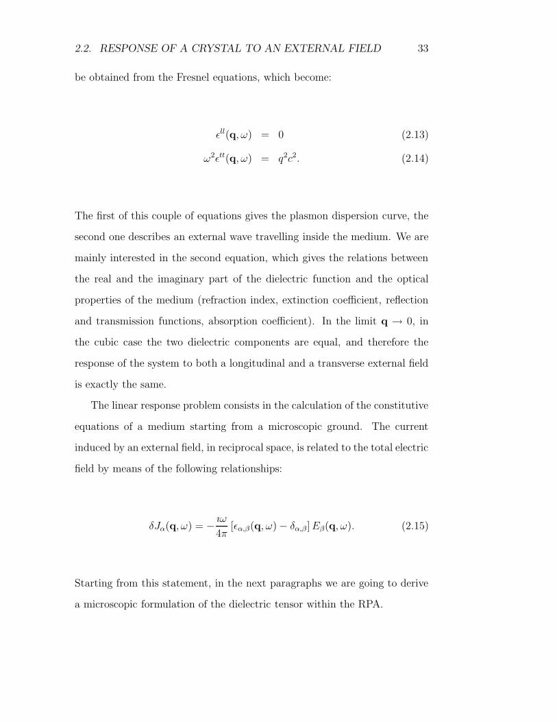
be obtained from the Fresnel equations, which become:
εll(q, ω) = 0 (2.13)
ω2εtt(q, ω) = q2c2. (2.14)
The first of this couple of equations gives the plasmon dispersion curve, the
second one describes an external wave travelling inside the medium. We are
mainly interested in the second equation, which gives the relations between
the real and the imaginary part of the dielectric function and the optical
properties of the medium (refraction index, extinction coefficient, reflection
and transmission functions, absorption coefficient). In the limit q → 0, in
the cubic case the two dielectric components are equal, and therefore the
response of the system to both a longitudinal and a transverse external field
is exactly the same.
The linear response problem consists in the calculation of the constitutive
equations of a medium starting from a microscopic ground. The current
induced by an external field, in reciprocal space, is related to the total electric
field by means of the following relationships:
δJα(q, ω) = − ıω
4π[εα,β(q, ω) − δα,β] Eβ(q, ω). (2.15)
Starting from this statement, in the next paragraphs we are going to derive
a microscopic formulation of the dielectric tensor within the RPA.

34 LINEAR RESPONSE THEORY
2.3 Interaction picture and correlation func-
tions
In the Schrodinger picture of quantum mechanics, the state of a system is
represented by the vector of an Hilbert space, which explicitly depends on
time. Using the Dirac notation, we write the state vectors and the operators
in the Schrodinger picture as:
|ΨS(t)〉 , OS. (2.16)
The operators in the Schrodinger picture do not have an explicit time depen-
dence, which is fully included into the state vectors through the Schrodinger
equation
ıh∂t |ΨS(t)〉 = H |ΨS(t)〉 , (2.17)
which contains the Hamiltonian operator H. Once that the initial conditions
of the problem have been fixed (namely, the state vector at t0), the formal
solution of Eq. (2.17) is
|ΨS(t)〉 = e−ıH(t−t0)/h |ΨS(t0)〉 . (2.18)
In the linear response problems, a quantum system is subject to an exter-
nal field, small enough to allow a perturbative approach. The Hamiltonian
operator has the form:
H = H0 + V , (2.19)
where H0 is the unperturbed Hamiltonian of the isolated system, while the
V term is due to the external field action. In these situations an extremely
2.3. INTERACTION PICTURE AND CORRELATION FUNCTIONS 35
useful picture is the interaction picture, whose basic idea consists in splitting
the time dependence between state vectors and operators. Using the unitary
transformation:
|ΨI(t)〉 = eıH0t/h |ΨS(t)〉 , (2.20)
and the corresponding operator transformation:
OI(t) = eıH0t/hOSe−ıH0t/h, (2.21)
it is easy to verify that only the perturbation term contributes to the time
dependence of the state vector, through the equation:
ıh∂t |ΨI(t)〉 = VI(t) |ΨI(t)〉 , (2.22)
while H0 gives the time dependence of the operators, through the motion
equation:
ıh∂tOI(t) =[
OI(t), H0
]
. (2.23)
The formal explicit solution of Eq. (2.22) is2:
|ΨI(t)〉 = T exp
− ı
h
∫ t
t0
dt1VI(t1)
|ΨI(t0)〉 , (2.24)
which is an expression well suitable to a series expansion. We assume that
the external potential is switched on at a finite instant of time τ . Therefore,
in the limit t0 → ∞, the starting state of the system is an eigenstate of H0.
Let us label the unperturbed states with the notation |Φm〉:
H0 |Φm〉 = E0m |Φm〉 . (2.25)
2 T is the Time-ordering operator, defined as:
T[
O(t1)B(t2)]
≡ θ(t1 − t2)O(t1)B(t2) − θ(t2 − t1)B(t2)O(t1),
θ is the Heaviside function.

36 LINEAR RESPONSE THEORY
We assume that the system is in its fundamental state |Φ0〉 before the per-
turbation is switched on, and so we can put
|ΨI(−∞)〉 = |Φ0〉 . (2.26)
In this way, we can write the state vector at the first perturbative order,
starting from the fundamental unperturbed state, as:
|ΨI(t)〉 =
(
1 − ı
h
∫ t
−∞
dt1VI(t1)
)
|Φ0〉 . (2.27)
The main quantities in the study of a physical quantum system are the
expectation values of hermitian operators. These are picture-independent
functions, and we shall see in the following the utility of using the interaction
picture. Let us consider a physical variable O, represented by an hermitian
operator O. In the perturbed system, the expectation value of O is
⟨
O⟩
(t) ≡⟨
ΨI(t)∣
∣
∣OI(t)
∣
∣
∣ΨI(t)
⟩
. (2.28)
By substituting Eq. (2.27), we can calculate the linear response of O to an
external field, and we find the result
⟨
O⟩
(t) =⟨
O⟩
0+
ı
h
∫ t
−∞
dt1
⟨[
VI(t1), OI(t)]⟩
0, (2.29)
where the right side expectation values have been calculated on the unper-
turbed fundamental state:
⟨
O⟩
0≡
⟨
Φ0
∣
∣
∣O
∣
∣
∣Φ0
⟩
0. (2.30)
Therefore, we obtain the quite general formula of the variation of a physical
quantity when the system is subject to the action of an external field:
δO(t) =ı
h
∫ ∞
−∞
dt1
⟨[
VI(t1), OI(t)]⟩
0Θ(t1 − t). (2.31)

2.4. THE DIELECTRIC TENSOR 37
2.4 The dielectric tensor
In this section, we shall see in detail the linear response of an electron non-
magnetic system subject to an external electromagnetic field. In order to
study the dielectric tensor for a generic medium, we consider an external
field, having both a longitudinal and a transverse component. We know that
the optical properties of a crystal are gauge-independent [31], so we choose
the gauge in which there is not any scalar potential. In this case the electric
field is related to the only vector potential through the relationship:
E(r, t) = −1
c
∂A
∂t(r, t). (2.32)
or, in the conjugate space,
E(q, ω) =ıω
cA(q, ω). (2.33)
The microscopic current density operator J(r), for a many body system
in an electromagnetic field, is defined as the sum of two terms [33]:
J(r) = J1(r) + J2(r), (2.34)
where
J1(r) = − e2
mc
N∑
i=1
A(ri, t)δ(r − ri)
J2(r) = − e
2m
N∑
i=1
[piδ(r − ri) + δ(r − ri)pi] .
(2.35)
N is the total number of electrons inside the crystal. When considering
the interaction with an external field, among the two components, only the
second term in Eq. (2.35), which we called J2(r), gives a linear contribution

38 LINEAR RESPONSE THEORY
to the energy. We can write the potential energy operator as3:
V (t) =1
c
∫
drJ2(r, t) · A(r, t). (2.36)
The current density linear response is the sum of the variations of its two
components. Using Eq.(2.31), we can write the induced current as:
δJα(r, t) = − e2N
mcΩAα(r, t) +
1
hc
∫
dr1dt1ΠRα,β (rt; r1t1)Aβ(r1, t1), (2.37)
where the first term comes out from the J1 contribution (Ω is the structure
volume), while the second term comes out from J2. We have introduced the
retarded current-current correlation tensor
ΠRα,β (rt; r′t′) ≡ −ı 〈[J2α(rt), J2β(r′t′)]〉0 Θ(t − t′). (2.38)
Using the well known Lehmann representation [34], by inserting a complete
set of unperturbed many-body eigenstates, we obtain the Fourier transform
of Eq. (2.38). In the following we neglect the local field effects, assuming a
local response in q-space, and we come to the result:
ΠRα,β (q; ω) =
∑
m
[
J2α(q)0mJ2β(−q)m0
ω − ωm + ıη− J2β(q)0mJ2α(−q)m0
ω + ωm + ıη
]
. (2.39)
We have defined the Fourier-transformed current operator J2(q):
J2α(q) = − e
2m
N∑
i=1
[
pie−q·ri + e−q·ripi
]
. (2.40)
The current density matrix elements between a couple of unperturbed many-
body states, whose transition frequency is ωm = (Em − E0)/h, are:
J2α(q)0m ≡⟨
Φ0
∣
∣
∣J2α(q)
∣
∣
∣Φm
⟩
. (2.41)
3 Here and in the following expressions, all the time-dependent operators are taken inthe interaction picture.

2.4. THE DIELECTRIC TENSOR 39
We consider here the one-electron approximation, in which the unper-
turbed states are Slater determinants of single particle functions, and the
induced current versus the electric field relationship becomes 4:
δJα(q, ω) =ıe2N
mΩωEα(q, ω)− ı
Ωω
∑
n,n′
(fn′−fn)
[
j2α(q)nn′j2β(−q)n′n
hω − Enn′ + ıη
]
Eβ(q, ω).
(2.42)
We have introduced the single particle current density matrix elements:
j2α(q)nn′ ≡ − e
2m
⟨
φn
∣
∣pαe−ıq·r + e−ıq·rpα
∣
∣φn′
⟩
, (2.43)
where |φn〉 is an unperturbed single particle state. We define fn as the
occupation of the nth unperturbed single particle level. At zero temperature,
for a semiconductor in its ground state, we know that fn = 1 for all the
occupied, valence states, while fn = 0 for the conduction states. In this
single particle picture, En is the single particle unperturbed energy, and we
have taken Enn′ ≡ En′ − En. Thus the final form for the dielectric tensor in
the RPA is [31]:
εα,β(q, ω) = (1 − 4πe2N
mΩω2)δα,β +
4π
Ωω2
∑
n,n′
(fn′ − fn)
[
j2α(q)nn′j2β(−q)n′n
hω − Enn′ + ıη
]
.
(2.44)
From this equation we can easily find the longitudinal-longitudinal compo-
nent of the dielectric tensor, that is a basic quantity needed for the study
of the crystal screening properties, and the transverse-transverse component,
related to the optical properties of the crystal. The longitudinal-longitudinal
component can be written in terms of the matrix elements of the charge
4 We use Eα as the α component of the external electric field E.
40 LINEAR RESPONSE THEORY
density operator, that we define as
ρ(q) = −ee−ıq·r. (2.45)
The charge conservation equation is the link between a linear response based
respectively on a current density or on a charge density formulation, as we
shall see later. It is not difficult to verify the following generalized sum rule:
∑
n,n′
(fn′ − fn)|q · j2(q)nn′ |2
Enn′
= −e2∑
n
fn = −Ne2, (2.46)
that leads us to write down the longitudinal-longitudinal dielectric function
in the following way:
εll(q, ω) = 1 +4πh2
Ω
(
E + iη
E
)2∑
n,n′
(fn′ − fn)
E2nn′
[
j2α(q)nn′j2β(−q)n′n
hω − Enn′ + ıη
]
.
(2.47)
In the limit of negligible broadening η, this latter equation can be well ap-
proximated by the following one, that is a fundamental result of the linear
response theory:
εll(q, ω) = 1 +4πh2
Ω
∑
n,n′
(fn′ − fn)
E2nn′
[
j2α(q)nn′j2β(−q)n′n
hω − Enn′ + ıη
]
. (2.48)
The longitudinal-longitudinal component could also be obtained starting
from the Coulomb Gauge (q · A = 0), and working only in terms of the
scalar potential. In this case, by studying the charge density response, and
introducing a density-density correlation function, a different relationship is
obtained for the longitudinal-longitudinal dielectric function. These two dif-
ferent formulations give identical results, because they only differ in a choice
of gauge, and the dielectric tensor is a gauge-invariant quantity. The way for

2.4. THE DIELECTRIC TENSOR 41
getting one formulation from the other is the charge conservation equation.
We write here such equation in the single particle operator form, connecting
the longitudinal component of the current density to the commutator be-
tween the Hamiltonian (h is the one-electron Hamiltonian) and the charge
density:
hq · j2(q) = [ρ(q), h] = ı∂
∂tρ(q). (2.49)
Using the expression (2.48) obtained before, together with the charge conser-
vation equation (2.49), we find the longitudinal-longitudinal dielectric func-
tion that is obtained within a charge density response formulation:
εll(q, ω) = δα,β +4πe2
q2Ω
∑
n,n′
(fn′ − fn)
[
|〈φn |e−ıq·r|φn′〉|2hω − Enn′ + ıη
]
. (2.50)
Coming back to Eq. (2.44), it is useful to derive the limit of very long
wavelengths, when q → 0, and we obtain the dielectric tensor5:
εα,β(ω) = δα,β +4πe2h2
Ωm2
∑
n,n′
(fn′ − fn)
E2nn′
[〈n|pα|n′〉 〈n′|pβ|n〉hω − Enn′ + ıη
]
. (2.51)
In the case of a cubic crystal, such as bulk silicon, the q → 0 dielectric tensor
reduces to the unit tensor times a scalar quantity, that is usually defined as
the dielectric function6:
ε(ω) = 1 +4πe2h2
3Ωm2
∑
n,n′
(fn′ − fn)
E2nn′
|〈n|p|n′〉|2[hω − Enn′ + ıη]
. (2.52)
5 In order to obtain this equation, we have used a procedure similar to that shownbefore for the longitudinal component of the dielectric function.
6 We use the following short notation for the square modulus of complex vector quan-tities:
|A|2 ≡3
∑
α=1
|Aα|2 .

42 LINEAR RESPONSE THEORY
As we have already pointed out, for cubic crystals, in the limit of long wave-
lengths, both the longitudinal and the transverse components of the dielectric
tensor give the same dielectric function defined in the fundamental equation
(2.52).
In the case of a bulk crystal, we explicitly write down the k-dependent
expressions. The longitudinal dielectric response, taking into account the
spin degeneracy through a 2 factor, is:
εll(q, ω) = δα,β+8πe2
q2Ω
∑
n,n′,k
[fn′(k + q) − fn(k)]
[
|〈nk |e−ıq·r|n′k + q〉|2hω − En′(k + q) + En(k) + ıη
]
,
(2.53)
while the dielectric function is (limit of long wavelengths):
ε(ω) = 1 +8πe2h2
3Ωm2
∑
n,n′,k
[fn′(k) − fn(k)] |〈nk|p|n′k〉|2Enn′(k)2 [hω − Enn′(k) + ıη]
. (2.54)
It is useful introducing, for each allowed transition, the Oscillator Strength
(OS), defined as:
Fnn′(k) =2 |〈nk |p|n′k〉|2
3mEnn′(k). (2.55)
In terms of the OS, we can write the dielectric function in the form:
ε(E) = 1 +4πe2h2
Ωm
∑
n,n′,k
[fn′(k) − fn(k)]Fnn′(k)
Enn′(k) [E − Enn′(k) + ıη]. (2.56)
2.5 Linear response and TB
The Tight Binding method, used as an empirical interpolation scheme, has
been a simple and powerful calculation tool for many years. In the form it
was first stated in the classical paper of Slater and Koster [1], the method
has been used to compute no more than crystalline band structures. Many
authors have been trying to enlarge the model in order to make it more
2.5. LINEAR RESPONSE AND TB 43
flexible. Indeed, the great simplicity of the SK approach, consisting in only
including into the scheme a (more or less) small number of Hamiltonian pa-
rameters, becomes an annoying limit when one asks something more than a
simple one-electron energy level calculation! The problem is the lacking of
an explicit knowledge of the basis wave functions, so that calculations of im-
portant quantities, such as, for example, charge densities, oscillator strengths
and dielectric properties, Coulomb and exchange interaction terms, are for-
bidden within this primitive scheme.
Over the years, many methods have been proposed, with the hope of
approximating the TB atomic orbitals, or, at least, the momentum matrix
elements, without rejecting the simple and powerful empirical way. A typi-
cal approach consists in performing an explicit calculation of the orthogonal
basis functions, by using, for instance, a Lowdin transformation of a basis
set of Gaussian or Slater orbitals, and choosing between a Slater-Koster or a
Pseudopotential Hamiltonian [25,35–39]. These approaches represent the at-
tempts of preserving the simplicity of the Empirical Tight Binding avoiding
the complications of an ab initio scheme, which requires a greater number of
basis orbitals [40], or the cumbersome study of localized functions [41, 42],
and the explicit construction of the Hamiltonian matrix.
A different method, much simpler, consists in directly fitting the mo-
mentum matrix elements, parametrized in such a way to reproduce oscillator
strengths, dielectric function, or k·p coefficients [22,43]. A recent usage, that
we shall analyze in detail in the following, starts from writing the momentum

44 LINEAR RESPONSE THEORY
operator using the relationship7:
p =ım
h
[
H, r]
, (2.57)
therefore changing the problem into the search of a suitable approximation for
the position matrix elements. The difference of this approach with respect to
the direct parametrization of the momentum matrix elements consists in the
inclusion of the Hamiltonian parameters into the Eq.(2.57). In other words,
we define the momentum using the informations on the Hamiltonian coming
out from the fitting of the band structure. This is a crucial point, because
the risk of each of the above mentioned methods is the setting of momentum
parameters disconnected from the Hamiltonian parametrization. In fact, the
use of the SK scheme for the energy levels calculations, together with a new
completely arbitrary parametrization for the momentum operator (or even
for the wave functions or the position operator) for the dielectric response
calculations can lead to problems of self-consistency with the theory, such
as, for example, the breaking of the gauge invariance of the dielectric tensor,
or the breaking of the charge conservation [44, 45]. A good setting of the
problem, from this point of view, was the one proposed by Hanke [36], who
used Gaussian functions for simulating atomic orbitals, choosing the Gaus-
sian coefficients in such a way to satisfy the charge conservation equation,
and this guaranteed the equality between charge density and current density
linear response. This is a good self-consistency check which each method
should comply to. Later, we shall come back on this point, showing how
much density and current response can change when charge conservation is
not verified.
7 From now on, we shall only consider single particle operators.

2.6. THE APPROXIMATION 45
2.6 The approximation
Between the many proposed approximations, we have used a very simple
one, that nevertheless allows us to get a good estimation of the bulk silicon
dielectric function. Although the method has been proposed some time ago
[27, 46], it has raised a new interest in recent years, with several researchers
that have been trying to give it a more formal justification [45, 47–49].
The starting point consists in writing the position operator as the sum of
two contributions [48]:
r = rc + rinter. (2.58)
that we define through their matrix elements in the TB basis set8:
〈σµR |rc| σ′µ
′R′〉 = Rµδσσ′δµµ′δRR′ (2.59)
〈σµR |rinter| σ′µ
′R′〉 = Dµµ′
σσ′ (R′µ′ − Rµ) . (2.60)
The first term rc contains the diagonal part of the position operator in the
basis set. The atomic orbitals are its eigenstates, with eigenvalues given by
the atomic positions. The second term, instead, takes into account the off-
diagonal contributions. The D vector matrix, defined in Eq. (2.60), rapidly
goes to zero on increasing the distance between the atoms. Its most important
contribution comes from the on-site terms Dµµσσ′(0). For the sp3 bulk silicon
basis set, there is only one independent off-diagonal on-site parameter:
(
D(x))00
sx(0). (2.61)
Therefore, we can divide all the position matrix elements into three different
contributions: (1) on-site, diagonal terms; (2) on-site, off-diagonal terms; (3)
8 We follow the formalism introduced in chapter (1) for TB atomic orbitals, using thelabelling Rµ = R + µ.
46 LINEAR RESPONSE THEORY
off-site, off-diagonal terms.
The approximation that we use consists in retaining only the first contri-
bution, and consequently treating the atomic orbitals as eigenstates of the
position operator in the dielectric properties calculations:
r ≈ rc. (2.62)
In this approximation, the third contribution with off-site terms, is supposed
to be of little importance, the main part of the position operator coming from
the on-site terms. There is an open discussion on whether or not including
the contribution (2) of on-site, off-diagonal terms [24,48–50]. From one point
of view, this is important in order to retrieve a non-null isolated-atom dipole
matrix element in the limit of very large lattice constant [24, 50]. From
another point of view, it has been shown that the inclusion of this term could
lead to troubles of consistency with the gauge-invariance of the theory [48,49].
In the case of an sp3 third neighbor basis set, we have verified that including
the additional term (2.61) only slightly modifies the bulk silicon dielectric
function (an almost rigid shift in the intensities is observed, while the peaks
positions are unchanged). For these reasons we have chosen to neglect such
contribution.
Starting from the approximation in Eq. (2.62) for the position, we define
the momentum matrix elements in the TB basis set via Eq. (2.57) :
〈σµR |p|σ′µ
′R′〉 =ım
h(R′
µ′ − Rµ)⟨
σµR
∣
∣
∣H
∣
∣
∣σ′
µ′R′
⟩
. (2.63)
We want to point out that the present approximation, performed on the po-
sition operator, allows us to include into the momentum all the informations
coming from the Hamiltonian parametrization, resulting into a momentum

2.7. THE CHARGE CONSERVATION 47
operator with many off-diagonal terms. We expect that this approach is for-
mally more correct than a direct parametrization of the momentum matrix
elements.
Within this on-site diagonal approximation for the position operator, p
assumes a very simple k-space representation, being proportional to the gra-
dient of the Hamiltonian matrix:
〈σµk| p |σ′µ
′k〉 =m
h∇kH
µµ′
σσ′ (k) . (2.64)
2.7 The charge conservation
We have seen in a previous section that the charge conservation condition
can be written as9:[
ρ(q), H]
= hq · j2(q). (2.65)
Because of the translational symmetry of the Bravais lattices, for a bulk crys-
tal the operator equation (2.65) has the following matrix elements between
couple of Bloch states:
⟨
nk
∣
∣
∣hq · j(q)
∣
∣
∣n′k + q
⟩
= 〈nk |ρ(q)|n′k + q〉 [En′(k + q) − En(k)] . (2.66)
Starting from the well known Baker-Hausdorff formula
eABe−A = 1 +[
A, B]
+1
2!
[
A,[
A, B]]
+1
3!
[
A,[
A,[
A, B]]]
. . . , (2.67)
it is easily verified that the charge conservation is equivalent to imposing two
conditions on the commutators between r and H:
[
rα, H]
=ıh
mpα (2.68)
[rα, pβ] = ıhδα,β. (2.69)
9 We have written here again the charge conservation Eq. (2.49), with the definitionof charge density and current density given in Eqs. (2.45) and (2.40).

48 LINEAR RESPONSE THEORY
In the limit of long wavelengths (q → 0), only the first one of this couple of
equations is needed to verify Eq. (2.65).
Within the approach presented here, we approximate the position r with
rc, whose eigenstates are exactly the TB atomic orbitals, and then we define
the momentum operator from Eq. (2.57). Therefore, by construction our
model verifies the charge conservation equation in the limit q → 0, and so it
is fully self-consistent in calculations of the long wavelength dielectric tensor
in Eq. (2.51). Instead, it does not verify the canonical commutator relations
in Eq. (2.69) between position and momentum operators. This means that,
for finite values of q, the charge conservation is not verified and we expect a
density response different from the current response.
In order to give a quantitative estimation of their relative shift, we have
analyzed both the current- and the density-derived longitudinal dielectric
function, with the help of Eq. (2.48) and (2.50), in the static limit ω = 0. In
figure (2.1) we show the longitudinal dielectric function that we have com-
puted using TB and EPM methods, in current and density representation.
It is clear that there is a unique EPM curve, because within the Local Pseu-
dopotential method the charge conservation is well defined, and both the
density and current responses give the same result. On the contrary, our TB
approach is charge-conserving only in the limit of long wavelengths, explain-
ing why we retrieve a unique static dielectric constant (q = 0). On the other
side, as Fig (2.1) clearly shows, the results are quite different on increasing
values of the transferred momentum. From a comparison between the TB
and EPM curves, it can be noticed that the TB current-derived dielectric
function is very close to the pseudopotential curve. Quite surprisingly, the

2.7. THE CHARGE CONSERVATION 49
Figure 2.1: Longitudinal dielectric function along the (100) direction, calculated
within both the density and current response approaches. We have used the Niquet
parametrization [28] for TB and the Chelikowsky Local form factors [12] for EPM
calculations. The green line refers to the EPM result, the blue and the red lines
are, respectively, the TB current and density responses.
difference between the two curves is almost a simple vertical shift. Instead,
the density response overestimates the EPM result. Somehow, this means
that for finite values of q the method gives a better estimation of current
than density operator.

50 LINEAR RESPONSE THEORY
2.8 Results
In this section we are going to show the bulk silicon dielectric function, cal-
culated using the so far described approximation, compared to EPM results
and experimental data. We write here again the complex dielectric function
for a bulk structure:
ε(E) = 1 +4πe2h2
Ωm
∑
n,n′,k
[fn′(k) − fn(k)]Fnn′(k)
Enn′(k) [E − Enn′(k) + ıη]. (2.70)
where we have used the oscillator strengths defined in Eq.(2.55). In particu-
lar, the imaginary part of the dielectric function can be written in the general
form:
ε2(E) =4π2e2h2
Ωm
∑
n,n′,k
[fn′(k) − fn(k)]Fnn′(k)
Enn′(k)S (E − Enn′(k)) , (2.71)
where S(x) is a broadening function, which is not necessarily a Lorentzian
function, depending on the sort of broadening that the electronic levels feel.
We here consider a Lorentzian broadening, and define S(x) as:
S(x) =η/π
x2 + η2. (2.72)
Starting from the commutation relations in Eq. (2.69), it is simple to show
that the following sum rule for the oscillator strengths holds:
∑
n′
Fnn′(k) = 1. (2.73)
Unfortunately, the present approximation does not verify Eq. (2.69), and
so the sum rule neither. The calculation of the right hand of Eq.(2.73) is a
good quantitative check on whether or not the oscillator strengths are well
reproduced within our method. The sum rule (2.73) can be written as an

2.8. RESULTS 51
overall condition on the dielectric function imaginary part (N is the number
of electrons contained inside the volume Ω)10:
mΩ
2Nπ2e2h2
∫ ∞
0
Eε2(E)dE = 1. (2.74)
In the case of the bulk silicon, we obtain for the left side of this equation
the value of 1.077, with both sets of TB parameters (Niquet and Tserbak
parameters), showing that the sum rule is satisfied to within 8%.
In figure (2.2) we report the imaginary part of the bulk silicon dielectric
function, calculated with EPM and TB. The experimental data are shown for
comparison. Only no-phonon transitions are considered in the calculation.
Phonon assisted transitions are expected to give a negligible contribution to
ε2. Indeed, the measured dielectric function does not show any significant
contributions at energies near the bulk Si indirect gap (at about 1.1 eV),
which are dipole-forbidden. The analysis of the experimental ε2(E) shows
two main peaks, that lie at energies of about 3.5 eV and 4.2 eV. Using both
empirical [36] and ab initio models [32], it is nowadays clear that the first
peak is due to excitonic effects, and can be theoretically calculated by only
inserting the electron-hole interaction inside the dielectric function. This is
not a simple task, and is well beyond the RPA approximation we are using.
Within RPA, we are only able to predict a shoulder in correspondence of the
first peak. Moreover, all the transition energies are slightly overestimated,
because the excitonic effects make the one-electron energy levels closer. Keep-
ing in mind these intrinsic limitations of RPA, we think, looking at figure
(2.2), that there is a good agreement between the two TB parametrizations,
EPM and experiments. Within the RPA, the solution we have chosen for
10 The real and imaginary part of dielectric function are indicated with ε1 and ε2 re-spectively.
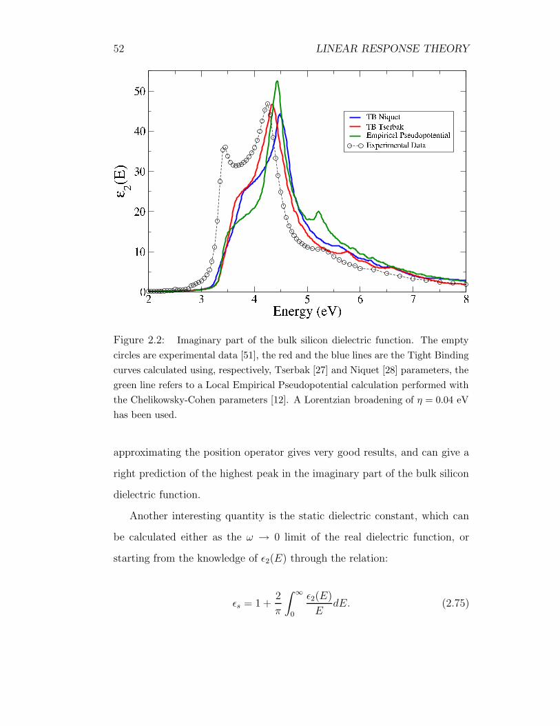
52 LINEAR RESPONSE THEORY
Figure 2.2: Imaginary part of the bulk silicon dielectric function. The empty
circles are experimental data [51], the red and the blue lines are the Tight Binding
curves calculated using, respectively, Tserbak [27] and Niquet [28] parameters, the
green line refers to a Local Empirical Pseudopotential calculation performed with
the Chelikowsky-Cohen parameters [12]. A Lorentzian broadening of η = 0.04 eV
has been used.
approximating the position operator gives very good results, and can give a
right prediction of the highest peak in the imaginary part of the bulk silicon
dielectric function.
Another interesting quantity is the static dielectric constant, which can
be calculated either as the ω → 0 limit of the real dielectric function, or
starting from the knowledge of ε2(E) through the relation:
εs = 1 +2
π
∫ ∞
0
ε2(E)
EdE. (2.75)

2.8. RESULTS 53
In table (2.8) we report on a comparison between the calculated values of
εs and the experimental value. Calculations have been performed with Ni-
quet [28] and Tserbak [27] parametrizations and with the Chelikowsky Local
Pseudopotential form factors [12], the experimental data is taken by [52]. An
error of about 10% is usually ascribed to excitonic effects.
Method εs
TB Niquet 10.74
TB Tserbak 10.63
EPM CC 10.53
Exp 11.40
Table 2.1: Bulk Si static dielectric constant.

54 LINEAR RESPONSE THEORY
Chapter 3
Spherical nanocrystals
3.1 Introduction
In this chapter we apply the Empirical Tight Binding method to the study
of Silicon spherical nanocrystals. In a first step, the nanocrystal energy lev-
els are calculated. The energy gap between the Highest Occupied Molecular
Orbital (HOMO) and the Lowest Unoccupied Molecular Orbital (LUMO)
is compared to the experimental data and to other theoretical results avail-
able in literature. The situation that comes out is quite chaotic, and a large
scatter of the many measured and calculated energy gaps can be observed.
Nevertheless, the ETB is seen to fit quite well most of the data, both for
small and large nanocrystals.
The second part of the chapter concerns the optical properties. A com-
parison of a nanocrystal extinction coefficient with an experimental result is
shown. This is a good check that the ETB works well. Then, the imagi-
nary part of the nanocrystal dielectric function is studied. On increasing the
nanocrystal size, the energy gap between the first transition energy and the
55

56 SPHERICAL NANOCRYSTALS
threshold of the absorption spectrum rapidly increases with it. This is an
interesting feature of the Si nanocrystals, and is related to the fast annihila-
tion of the oscillator strengths and to the rise of the radiative recombination
time. The matter is discussed in detail, investigating the projection of the
nanocrystal states on the bulk states. It comes out that the k-space overlap
between the HOMO and LUMO states rapidly nullifies, when the nanocrys-
tal size increases. This behavior can well explain the exponential increase
of the radiative recombination times. Finally, the static dielectric constant
has been studied, and a comparison with other theoretical calculations is
discussed.
3.2 The method
The application of the ETB to the nanocrystals is very simple. A nanocrystal
can be thought of as composed by three parts: (1) an inner core, (2) a relaxed
shell, and (3) a passivant layer. Inside the inner core the atoms behave as
in the bulk, being the surface far enough that its effects are negligible. The
relaxed shell covers the nanocrystal core, and the surface effects have to be
taken into account. The atoms in the shell relax from their bulk positions,
and a modulation of the Hamiltonian parameters is expected. Finally the
nanocrystal is covered by a passivant layer, usually constituted by Hydrogen,
Oxygen or Si dioxide. From an experimental point of view, the nanocrystals
are always passivated, and the species covering the structures are determined
by the experimental setup. The inclusion of the passivant layer into a theo-
retical model is very important, in order to avoid the appearance of dangling
bonds (uncovered Si atoms), or bonds with other species (for instance, a sin-

3.2. THE METHOD 57
gle Oxygen on a fully Hydrogenated surface). The presence of even a single
dangling bond on the nanocrystal surface leads to the formation of a local-
ized state with energy well inside the gap. These localized states work as
electron traps, decreasing the nanocrystal optical efficiency and activating
non-radiative recombination channels.
The ETB approximation in the study of nanocrystals consists on mod-
elling the nanocrystal as formed by only an inner core and a passivant layer.
Therefore, the method neglects the surface effects, and we shall not take
into account the relaxation effects on the atomic positions, with the con-
sequent modulation of the Hamiltonian parameters. This idea of transfer-
ability [4] of the Hamiltonian parameters from the bulk to the nanostruc-
tures indeed works well, as it has been shown by years of applications of
ETB [21, 23, 24, 28, 43, 53–57].
For our calculations, we have used the sp3 3rd nearest neighbor ETB [28],
which give a good estimation of the Bulk Si fundamental band gap and ef-
fective masses. We have studied spherical nanocrystals with a Si atom in
the center, with the surface passivated by Hydrogen atoms. We have taken
for Hydrogen only the 1s orbital, using the Si-H interaction parameters from
Niquet [28], which have been chosen in such a way to reproduce the SiH4
absorption spectra.
From the computational point of view, we have factorized the Hamilto-
nian matrix according to the five irreducible representations of the Td sym-
metry group. Using the group theory, we have been able to reduce the size of
the diagonalization problem, label the energy levels of the nanocrystal, and
therefore use the selection rules for studying the dipole-allowed transitions.

58 SPHERICAL NANOCRYSTALS
The ETB method is a very efficient tool in the study of nanocrystals. In fact,
the method needs very few atomic orbitals for each atom in the structure.
Within the sp3 parametrization, only 4 functions are required for each silicon
atom. This leads to very small matrices compared, for instance, to the Plane
Wave methods, where at least one hundred basis functions are required for
each atom. Moreover, the TB matrices show a huge degree of sparsity, which
can be used to further reduce the computational effort1. This has been done
using an iterative diagonalization routine, which makes a heavy use of the
sparsity for calculating the first m eigenvectors of a N ×N matrix. Starting
from the Hamiltonian matrix H, we have applied a folding procedure, near
a reference energy ε. We calculate the square matrix:
H2 = (H − ε)2, (3.1)
and from the eigenvalues of H2 we easily retrieve the H eigenvalues. With
this procedure we reduce the problem of calculating a set of eigenvalues in
the neighborhood of an energy reference, to the problem of calculating the
first m eigenvalues of a given matrix. Making use of the sparsity, the overall
computational time is reduced to a linear scaling:
t ∝ m2N, (3.2)
which is much faster than the t ∝ N 3 trend of the standard computational
routines. In order to have an idea of the ETB efficiency, we want to give some
numbers. Let us consider Si1707H628, a spherical nanocrystal with a 4 nm
1 We have seen that an interaction up to 3rd neighbors allows us to well reproducethe Si-Si Hamiltonian matrix elements, as it results from the fair agreement of the gapenergies and the effective masses with the experimental results. Moreover, the use of afinite interaction range allows to put equal to zero all the further interactions, leading tovery sparse matrices.

3.3. ENERGY LEVELS 59
Figure 3.1: HOMO and LUMO states for spherical nanocrystals on varying their
diameter. The lines are guides for the eyes.
diameter. The Hamiltonian matrix for this nanocrystal has a size N = 7456,
with 664448 non null elements. This means that only the 1.2% of the whole
matrix is different from zero! A larger nanocrystal is Si5707H1372, with a
d = 6 nm diameter. In this case the size of the problem is N = 24200, and
the number of non null elements is only the 0.4% of the whole matrix.
3.3 Energy levels
In a first step, we have calculated the energy levels for a set of hydrogenated
spherical nanocrystals, with increasing size. For each nanocrystal, the effec-
tive diameter is calculated as follows [28,58]. In the bulk, ideal structure, the
volume associated to each Si atom is vSi = a3/8 (a ' 0.5431 nm is the Si lat-

60 SPHERICAL NANOCRYSTALS
tice constant). A good estimation of the nanocrystal volume can be vSiNSi
from which, assuming a spherical shape, the diameter is easily calculated
using the relation [28]:
d = a
(
3
4πNSi
)1/3
= 0.33691N1/3Si . (3.3)
In Fig. 3.1 we show the energy levels, labelled according to the five irreducible
representations of the Td symmetry group. The quantum confinement effect
is well visible. In fact, on increasing the nanocrystal size, the HOMO energies
increase, while the LUMO energies decrease, and the gap energy goes down
to the bulk value of 1.1 eV.
In figure 3.2 we show the calculated first transition energy for spherical
nanocrystals with increasing diameter. Our theoretical results have been
indicated by means of crosses, while the solid line is a fit of the numerical
data [28]. We compare the first transition energy to different sets of exper-
imental results, coming from both photoluminescence (PL) and absorption
(Abs) measurements. We want to point out the great difficulty in such a
comparison. In fact, in literature there is a large scatter of the experimen-
tal data, caused by the different experimental setup that make the repro-
ducibility of the measurements a formidable task. For instance, we expect
different results between Porous Silicon (PSi) samples2, and Si nanocrystal
(Si nc) samples. Another point is the kind of measurements performed on
the samples. As a matter of fact, it is generally observed an energy differ-
ence, named the Stokes shift, between the absorption threshold and the main
photoluminescence emission peak energy, with an effect that is stronger for
smaller nanocrystals [57, 60–62]. It is of great interest to compare both the
2 PSi has been shown with many experimental evidences to be constituted by Sinanocrystals [59].

3.3. ENERGY LEVELS 61
Figure 3.2: The first dipole-allowed transition energy (optical gap) for different
nanocrystals with increasing size (crosses). The solid line is a fit of the calcu-
lated data. The experimental absorption (open symbols) and photoluminescence
emission (filled symbols) are also shown for comparison. Squares are from [63],
triangles-up from Ref. [64], open diamonds from [65], triangles-down from [66],
filled circles from [67], filled diamonds from [68].
absorption and the photoluminescence data. In Fig. 3.2 we have included
two couples of absorption and photoluminescence measurements (triangles-
up and squares) performed on the same sample. From the theoretical point
of view it is not completely clear the origin of the Stokes shift, even if many
models have been proposed.
In the recent years, the fundamental role of the surface on the optical
properties of nanocrystals has been becoming clearer. The presence of even
just one Oxygen atom on an Hydrogenated surface can lead to a significantly

62 SPHERICAL NANOCRYSTALS
Figure 3.3: Spherical nanocrystals optical gap: comparison with other calcu-
lations. We have shown our calculated first dipole-allowed transition energies by
open circles, while the solid line is a fit. Density functional data: red squares
are taken from [70], green diamonds from [71], triangles-up from [72], triangles
left from [73], yellow triangles-down from [74], green squares from [62]; Empirical
Pseudopotential: triangles-right from [16], blue squares from [75]; the Quantum
Monte Carlo results (pink triangles-down) are taken from [76].
red-shift of the optical gap, especially for small nanocrystals [69]. And an
exposure in air of a sample, even for a few minutes, can decrease the PL
peaks energies up to 1 eV [66]. In this respect, the triangles-down data of
Wolkin [66] come out from carefully cleaned, Oxygen-free samples. The fair
agreement of the present calculation with the Wolkin data is indeed an im-
portant experimental check that the method does indeed work well.
In Fig. 3.3 we show a comparison between our results and other theo-
retical results for Hydrogenated, spherical Si-nc. Also in this case there is

3.4. DIELECTRIC FUNCTION 63
a large scatter of the calculated data, and this is especially true for the ab
initio methods. Some considerations can be inferred by the graph. First
of all, there is a good agreement with the other important semiempirical
method, based on the Pseudopotentials (PP). In figure, PP calculations with-
out (triangles-right) [16] or with the inclusion of the Coulomb e-h interaction
(squares) [75], have been shown in blue. It is worth noting that the PP trend
is very similar to our results, with a better agreement for larger nanocrys-
tals. The situation for small nanocrystals is more complicated. Even for
data reproduced within the same approach, like the Time Dependent Den-
sity Functional Theory (TDDFT), we can have quite different results. For
instance, the Garoufalis [72] and Vasiliev [70] results are at higher energies
then the Benedict [74] calculations. The methods differ in the choice of the
Exchange-Correlation Kernel, and for an alternative definition of the optical
gap, in the case of Ref. [70]. Instead, for the local density approximation
(LDA), the problem consists in the lacking of an exact theoretical definition
of the optical gap. The various approaches are based on a different definition
of the optical gap [62, 71, 73], and there is an open debate on the subject.
Looking at Fig. 3.3, it is interesting to note that our curve goes through
all these data. In particular, we want to underline the fair agreement of our
calculation with the most recent TDLDA calculations of Benedict [74], and
the LDA results of Degoli [62].
3.4 Dielectric function
We have applied our TB method to the study of the nanocrystal dielec-
tric function. As a check of our method, we have considered the Si159H124

64 SPHERICAL NANOCRYSTALS
nanocrystal (which has an equivalent diameter of 1.83 nm), and compared
the calculated extinction coefficient (related to the dielectric function) to
an experimental curve, given by Wilcoxon for a silicon nanocrystal with a
diameter of about 1.8 nm. In Fig. 3.4 the two curves are shown. The ar-
row indicates the first calculated transition energy. We have rescaled our
theoretical data in such a way the two curves have the same height of the
main peak. We want to point out the great similarity of the two curves. In
fact, an overestimation of the calculated dielectric function is intrinsic of our
parametrization, as it was clear already for the bulk, from Fig. 2.2. Never-
theless, there is a fair agreement in the relative intensities of the two main
peaks, and in the overall broadening of the two curves.
In Fig. 3.5 we show the imaginary part of the dielectric function for a set
of spherical silicon nanocrystals. A black solid arrow shows the first dipole
allowed transition energy. On increasing the nanocrystal size, the first tran-
sition energy goes down quite fast, approaching the electron-forbidden bulk
indirect band gap of 1.1 eV. On the other hand, the onset of the imaginary
part of the dielectric function (and the threshold of the absorption coefficient)
is much less sensitive to the size. A quantitative evaluation of the absorp-
tion threshold can be done using an experimental technique, consisting in
calculating the integral absorption cross section. In fact, for molecules and
direct gap semiconductors the absorption threshold is usually defined as the
energy of the first allowed transition. However, in the case of Si, which has
an indirect-gap behavior, we find a large number of very weak transitions at
low energy. The indirect-gap behavior is well visible even for Si nanocrystals,
leading to an experimentally observed onset of the absorption well above the
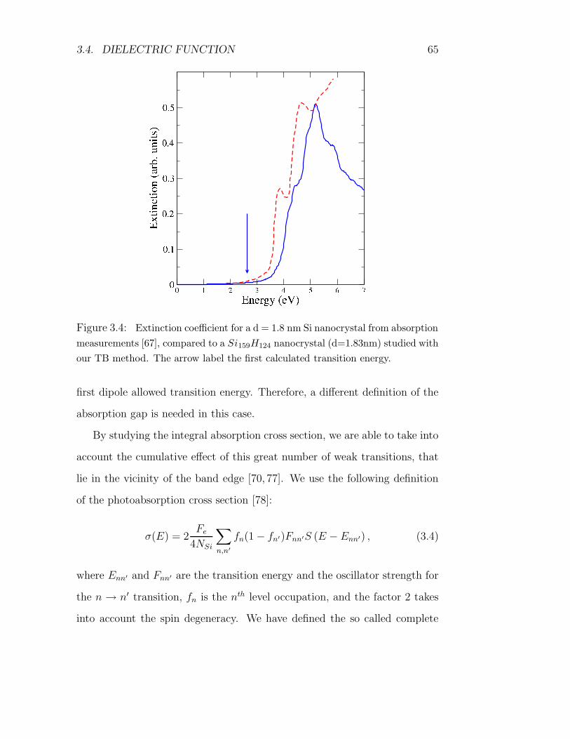
3.4. DIELECTRIC FUNCTION 65
Figure 3.4: Extinction coefficient for a d = 1.8 nm Si nanocrystal from absorption
measurements [67], compared to a Si159H124 nanocrystal (d=1.83nm) studied with
our TB method. The arrow label the first calculated transition energy.
first dipole allowed transition energy. Therefore, a different definition of the
absorption gap is needed in this case.
By studying the integral absorption cross section, we are able to take into
account the cumulative effect of this great number of weak transitions, that
lie in the vicinity of the band edge [70, 77]. We use the following definition
of the photoabsorption cross section [78]:
σ(E) = 2Fe
4NSi
∑
n,n′
fn(1 − fn′)Fnn′S (E − Enn′) , (3.4)
where Enn′ and Fnn′ are the transition energy and the oscillator strength for
the n → n′ transition, fn is the nth level occupation, and the factor 2 takes
into account the spin degeneracy. We have defined the so called complete

66 SPHERICAL NANOCRYSTALS
Si29H36
d=1nm
Si47H60
d=1.2nm
Si87H76
d=1.5nm
2 4 6 80
10
20
30Si147H100
d=1.8nm
Si191H148
d=1.9nm
Si357H204
d=2.4nm
Si465H252
d=2.6nm
2 4 6 80
10
20
30Si705H300
d=3nm
Energy (eV) Energy (eV)
ε2
Figure 3.5: Imaginary part of spherical nanocrystals dielectric function, on
increasing diameters. A 0.1 eV Lorentzian broadening has been used. The black
arrows show the first dipole allowed transition, while the red arrows show the
absorption threshold.
one electron oscillator strength Fe [77, 79] as:
Fe =2π2he2
mc' 1.098eV A2. (3.5)
We suppose that the nanocrystal is embedded in a dielectric medium with a
refraction index n = 1, and we neglect local field effects. Starting from the
one electron cross section in Eq.(3.4), we define the absorption gap as the
energy Eg such as:∫ Eg(p)
0
σ(E)dE = pFe. (3.6)
This procedure allows the determination of an energy Eg(p), that depends on
the external parameter p. We expect that p is related to the precision of the
3.5. OSCILLATOR STRENGTHS 67
experimental set up (in other words to the smallest oscillator strength which
can be detected). We use the value p = 10−4, which is consistent with the
experimental measurements [79,80]. For each nanocrystal we have calculated
the absorption gap. In Fig. 3.5, for each nanocrystal, we use a red dashed
arrow to show the absorption gap. As we expected, the absorption gap
lies exactly on the threshold of the imaginary part of the dielectric function.
While for small structures, Eg lies quite close to the first transition energy, for
large nanocrystals the energy gap between the two curves becomes very large.
This is due to a huge number of very weak low energy transitions that, on
increasing the nanocrystal size, tend to become zero. This interesting feature
of Si nanocrystals will be analyzed in more detail in the next sections.
3.5 Oscillator strengths
In order to better understand the optical behavior in the vicinity of the
band edge, we have calculated the first Oscillator Strengths (OS) and the
radiative recombination times. In Fig. 3.6, on the right side, we show the
OS versus the transition energies. On increasing the nanocrystal diameter,
the quantum confinement effects lead to a decrease of the transition energies.
At the same time, also the OS decrease, but much faster. This result is in
a good agreement with the first DFT calculations of Delley [81]. Moreover,
very recently Dovrat has reported on OS measurements as a function of
the transition energy, which show an exponential dependence [80]. Even if
the experimental conditions are quite different (nanocrystals embedded in
a silicon dioxide matrix) and the considered sizes are larger than the ones
studied here, it seems that both the trend and the order of magnitude are

68 SPHERICAL NANOCRYSTALS
2.0 2.5 3.0 3.5 4.0 4.5Energy (eV)
10-1
101
103
105
2.0 2.5 3.0 3.5 4.0 4.5Energy (eV)
10-7
10-5
10-3
10-1
Recombination Rate (ms-1
) Oscillator Strength
Figure 3.6: First lowest-energies recombination rates (left) and oscillator
strengths (right) of spherical silicon nanocrystals on varying the diameter. Si29H36
(d = 1.0 nm), squares; Si87H76 (d = 1.5 nm), circles; Si191H148 (d = 1.9 nm),
triangles-up; Si465H252 (d = 2.6 nm), triangles-right; Si705H300 (d = 3 nm), dia-
monds.
in a good agreement with our results. For instance, Dovrat finds an OS of
about 4×10⁻³ for a transition energy of about 1.9 eV, where we find a value
of 5 × 10⁻³ at 1.95 eV.
On the left side of Fig. 3.6, we show our calculated recombination rates,
that we define as the inverse of the radiative recombination time [78]:
1
τrad
=2e2
h2mc3E2
vcFvc. (3.7)
We have calculated it for the lowest energies transitions from occupied to un-
occupied states. On increasing the nanocrystal size, the transition energies
decrease, their recombination rates decrease and the radiative recombination

3.6. K-SPACE PROJECTIONS 69
time increases. Already for a 3 nm nanocrystal, with energies at about 2
eV, we have the recombination time τrad ' 10µs. When the nanocrystals
size changes from a few A to several nanometers, the radiative recombina-
tion times change from the range of the ns (d ' 1 nm) to the µs (d ' 3
nm) to the ms (bulk Si). Even in this case a comparison with the experi-
mental data would be of huge interest. Radiative recombination times for
Si Hydrogenated spherical nanocrystals have already been calculated in the
past [53], and a comparison between experiments and theoretical results has
been recently tried [73].
3.6 k-space projections
The decrease of the oscillator strengths and the increase of the radiative re-
combination times, on increasing the nanocrystal size, can be well explained
looking at the projection of the nanocrystal eigenvectors on the bulk states.
The TB interpolation scheme gives the eigenfunctions of the bulk Si Hamil-
tonian in terms of the atomic orbital basis set. In ket notation, joining the
equations (1.6) and (1.9), we can write:
|nk〉 = C∑
σ,R,µ
Bµσn(k)eık·Rµ |σµR〉 , (3.8)
where C is a normalization constant depending on the structure volume,
and the sum is done all over the atomic orbitals. Instead, we can write the
expansion:
|mλ〉 =∑
σ,R,µ
Cλσm(Rµ) |σµR〉 , (3.9)
for the mth nanocrystal state of the λ irreducible representation of the Td
symmetry group, where the eigenvectors come out from the diagonalization

70 SPHERICAL NANOCRYSTALS
procedure. In order to quantitatively understand how much a nanocrystal
state is far from a bulk state, we define the projection operator:
P (k) =∑
n
|nk〉 〈nk| . (3.10)
The sum is done on the whole band-complex constituted by the top valence
and the lowest conduction bands. We sum over the 8 calculated Tight Bind-
ing bands. This projection operator gives the nanocrystal states component
on Bloch states with a fixed value of the crystalline momentum k. It is im-
portant to note that for the confined systems the crystalline momentum is
not a good quantum number, due to the lack of periodicity. Nevertheless,
being both the bulk crystal Bloch states and the nanocrystal states expressed
as a linear combination of the same atomic wavefunctions (see Eqs. (3.8) and
(3.9)) the projection operator (3.10) allows to understand the size for which
bulk states are almost retrieved. It is expected that beside a threshold size,
the quantum confinement effects become negligible, and almost Bloch-like
states are observed.
From Fig. 3.1 the behavior of spherical nanocrystal HOMO and LUMO
states was visible. While the HOMO states have a quite size-independent T2
symmetry, the LUMO states indifferently show an A1, E1 or T2 symmetry,
according to the diameter [28,82]. Nevertheless, it is quite clear that, except
for very small structures (with a few Si atoms), we have a 6 quasi-degenerate
LUMO level, where the first six A1 + E1 + T2 states are very close in energy.
This is fully consistent with the EMA theory, which gives the prediction of
such sixfold degenerate LUMO states, due to the existence of six minima
in the Bulk Si first conduction band. So, we have calculated the k-space
projection for both (1) the threefold degenerate HOMO states and (2) the

3.6. K-SPACE PROJECTIONS 71
0.0 0.2 0.4 0.6 0.8 1.0 1.2 1.4k [100]
0.0
0.2
0.4
0.6
0.8
1.0P(
k)Si
47H
60 d = 1.2 nm
Si87
H76
d = 1.5 nmSi
191H
148 d = 1.9 nm
Si357
H204
d = 2.4 nmSi
705H
300 d = 3.0 nm
ΧΓFigure 3.7: k-space projection of the eigenstates for nanocrystals with different
sizes. The dashed and the solid lines are respectively the projections of the HOMO
and LUMO states. The normalization has been done in such a way that the HOMO
states projection is 1 in Γ.
sixfold quasi-degenerate LUMO states:
P (k) =∑
m,λ
⟨
mλ∣
∣
∣P (k)
∣
∣
∣mλ
⟩
. (3.11)
The sum is done over all the 3 degenerate (or the 6 quasi-degenerate) states.
In Fig. 3.7 the ∆ line projection is shown for both the HOMO and
LUMO states, for our set of spherical nanocrystals. The HOMO states have
component especially at Γ, whereas the LUMO states have fundamentally an
X behavior. It is worth noting that, on increasing the nanocrystal diameter,
the overlap between HOMO and LUMO states annihilate in a quite fast way.

72 SPHERICAL NANOCRYSTALS
Together with this, we want to point out that the LUMO projection is well
centered on X when the nanocrystal size is smaller than a certain threshold.
For diameters higher than this threshold, the maximum of the LUMO states
goes away from X, tending to the bulk limit of about 0.83. Therefore, we can
differentiate the behavior of Si nanocrystals. For small sizes, there is a good
k-space overlap of the HOMO and LUMO states, leading to non negligible
OS strengths, recombination times of µs or ns and the absorption gap close
to the HOMO-LUMO transition energy. For large sizes, instead, there is
a very small overlap of the HOMO and LUMO states, the LUMO states
tend to be centered at k = 0.83, the OS are very small, while the radiative
recombination time becomes of the order of ms. The nanocrystals retrieve
the bulk Si indirect gap behavior. This is very clearly understood from Fig.
3.7.
3.7 Dielectric constant
In recent years, a huge interest has been devoted to the study of the Si
nanocrystal screening properties [58, 83–85]. This is an important task, be-
cause it is related to the calculation of the electron-hole interaction energy.
We have calculated the static dielectric constant εs for our spherical nanocrys-
tals. In Fig. 3.8 we show our results (with circles), together with other the-
oretical curves. We have rescaled the values in order to retrieve the experi-
mental bulk limit. We have shown in figure the Empirical Pseudopotential
calculations (PP) of Ref. [58], the generalized Penn model (GPM) [58], and
the self-consistent TB results of Ref. [83]. The PP calculations have been per-
formed using the same procedure that we have used here, starting from the

3.7. DIELECTRIC CONSTANT 73
Figure 3.8: Calculated static dielectric constant for Si spherical nanocrystals.
Circles correspond to our Tight Binding results (the line is only a guide for the
eyes). The green lines are the Pseudopotential fits from Ref. [58] The black line
corresponds to the generalized Penn model [58] while the red line is a calculation
performed within a self-consistent potential Tight Binding model [83]. The bulk
limit of 11.4 has been shown for comparison.
imaginary part of the RPA dielectric function and calculating the dielectric
constant through Eq. (2.75). Indeed the agreement is quite good. The GPM
is a model based on the nearly free electron gas for the band energies [86],
and is expected to give good results in the limit of large nanocrystals. In-
stead, the self consistent TB [83] is applied to the problem of the nanocrystal
screening by an hydrogenic impurity, and gives quite different results.

74 SPHERICAL NANOCRYSTALS
Chapter 4
Ellipsoidal nanocrystals
4.1 Introduction
In this chapter the optical and infrared properties of silicon ellipsoidal nanocrys-
tals are illustrated. First, the anisotropy of the Photoluminescence from
Porous Silicon samples is briefly described. This phenomenon can be con-
sidered as the experimental evidence of the realization of silicon ellipsoids,
motivating our interest in this field. The nanocrystals that we have studied
have a revolution axis along the [001] lattice direction. In a first step, the
ellipsoidal axes lying in the plane perpendicular to the [001] direction have
been kept fixed to a value of 2 nm, while the axis along the symmetry direc-
tion has been varied.
The optical properties of these nanocrystals have been studied, and the
dependence of the dielectric tensor anisotropy on the geometrical anisotropy
has been carefully analyzed. A particular interest has been focused on the
onset of the absorption cross section, which has a significant dependence on
the structure aspect ratio. A comparison between ellipsoids and quantum
75

76 ELLIPSOIDAL NANOCRYSTALS
wires is illustrated, showing that the quantum wire limit is reached for not
large values of the aspect ratio. Next the static dielectric constant has been
investigated. This is the first time that a similar calculation is performed. It
can be of great importance in the study of the screening properties of ellip-
soidal nanocrystals.
A second part of the work has been focused on the LUMO states and
the infrared intraband transitions for very large ellipsoidal nanocrystals. A
set of fixed semiaxes nanocrystals, and a set of fixed volume ellipsoids have
been studied. The equivalent diameter of the structures is about 6 nm, and
nanocrystals with up to tens of thousands of Si atoms have been analyzed.
We have verified that for such huge sizes the Empirical Tight Binding gives
results fairly consistent with the Effective Mass Approximation predictions.
4.2 Porous Silicon Photoluminescence
We want to begin the discussion on the optical properties of Si ellipsoids by
pointing out their experimental evidence. Since its discovery in 1990 [88],
the huge Photoluminescence (PL) from Porous Silicon samples (PSi) was
explained in terms of Quantum Confinement Effect (QCE), assuming that
quantum wires or, better, small photoluminescent nanoparticles are respon-
sible of the Photoluminescence from porous silicon. Over the years, many
alternative models have been suggested as at the origin of the PSi PL, such
as hydrogenated amorphous silicon, defects, luminescent molecules or surface
states [59]. But, after years of experimental and theoretical work, nowadays
the QCE hypothesis is the most accepted one to explain the PL. Among the
many proofs, TEM images have clearly shown the presence of Si nanocrystal-

4.2. POROUS SILICON PHOTOLUMINESCENCE 77
Figure 4.1: PL Anisotropy from a Porous Silicon layer (results taken from Ref.
[87]). The sample has been exposed to an exciting radiation with a polarization
vector parallel (upper figure) or perpendicular (lower figure) to the [100] growth
direction. The PL radiation, with either parallel or perpendicular polarization
with respect to that one of the exciting light, has been detected. The resulting
degree of linear polarization of the detected light with respect to the exciting light,
defined in Eq. (4.1), is also shown in figure.
lites in PSi samples. In addition, the great similarity of the PL from PSi and
Si nanocrystals (Si-nc) has been supported by numerous evidences [89]. Nev-
ertheless, an important difference exists between the two kinds of PL. While
in the case of Si-nc an isotropic PL is observed, PSi samples are characterized

78 ELLIPSOIDAL NANOCRYSTALS
by a strong PL anisotropy. The reason at the basis of this phenomenon is
quite clear, in that a porous silicon layer has a preferred orientation along the
growth direction. We expect the formation of quantum wires, and pores, and
elongated structures with a revolution axis parallel to the growth direction.
In an important paper, Kovalev [87] measured the PL polarization for a PSi
layer having a [100] growth direction. In Fig. 4.1 we report on the results of
that paper. The degree of linear polarization has been defined as:
ρ =I‖ − I⊥I‖ + I⊥
, (4.1)
where I‖ (I⊥) is the PL radiation polarized parallel (perpendicular) to the
exciting light polarization. From Fig. 4.1 it clearly results a change of sign of
ρ, when the exciting radiation changes its polarization from parallel to per-
pendicular, with respect to the [100] direction. This behavior is a clear proof
of the strong PL anisotropy from PSi, whose emission radiation has a pre-
ferred [100] polarization. Kovalev [87] showed that the degree of anisotropy
could be fairly fitted assuming that the PSi PL comes from a distribution
of ellipsoidal Si nanocrystals, which can have either an elongated or a flat-
tened shape. Most of the ellipsoids have a symmetry axis parallel to the [100]
growth direction.
4.3 Silicon ellipsoids
We have applied our TB method to the study of Si ellipsoidal nanocrystals,
having a rotational symmetry axis along the [100] direction. The ellipsoid
surface is defined by the equation:
x2 + y2
a2+
z2
c2= 1, (4.2)
4.3. SILICON ELLIPSOIDS 79
where the origin of the coordinates has been taken on a Si atom. Here, a
and c are the semi-axes along, respectively, the parallel and the perpendic-
ular direction with respect to the symmetry axis. An important feature of
the structures is χ = c/a, the ellipsoid aspect ratio, which is a measure-
ment of their geometric anisotropy. The ellipsoid symmetry group, within
the TB approximation (in which the atoms do not relax from their bulk posi-
tions), is D2d, a subgroup of the full Bulk Si point group. D2d is constituted
by 8 elements, and 5 irreducible representations (IR): the unidimensional
A1, A2, B1, B2 and the unique bi-dimensional E1 (see Appendix B for the
character table and the symmetries related to the IR). The irreducible repre-
sentations will be used to label the energy levels, and to define the transition
rules.
In the first part of the work, a set of ellipsoidal nanocrystals, having a
fixed value of the semiaxes lying in the xy plane, has been studied. A value
a = 1 nm has been chosen, and the optical properties of the ellipsoids have
been investigating on varying the aspect ratio χ. From a geometrical point
of view, the nanocrystals tend to a quantum disk, in the limit of very small
values of χ. In the opposite limit, χ → ∞, the ellipsoids go to the cylindrical
quantum wire, having a circular radius of 1 nm. The number of Silicon atoms
increases almost linearly with the aspect ratio. Therefore, the signature of
both the anisotropy due to the different sizes of the ellipsoids along different
directions, and a quantum confinement effect, caused by the increase of the
total number of atoms, is expected to be found in the optical properties.
In Fig. 4.2 the energy levels for the ellipsoids are shown. It is worth
noting that, at least in the studied range of aspect ratios, both the LUMO

80 ELLIPSOIDAL NANOCRYSTALS
1.6
1.8
2
Ene
rgy
(eV
)A
1
A2
B1
B2
E1
-0.5
-0.4
Ene
rgy
(eV
)
0 1 2 3 4 5 6χ
Figure 4.2: Energy levels for a set of silicon ellipsoidal nanocrystals, with a = 1
nm, as a function of the aspect ratio χ. The lines are guides for the eyes.
and the HOMO energy levels have a well defined symmetry, as we already
noted for spherical nanocrystals. In fact, the lowest unoccupied states form a
quasi-degenerate energy level, with the 4 states coming from the A1+B1+E1
representation. Instead, the top of the occupied states has a bi-dimensional
E1 symmetry. And both the first LUMO and HOMO states are well sepa-
rated from the other levels1. From Fig. 4.2 it clearly appears the quantum
confinement effect, related to the increase of the number of Si atoms with
1 It is worth noting that, as we have recently shown [90,91], there is a correspondenceof the LUMO states calculated within TB, and within the EMA. Each EMA state comesout from a single bulk conduction band minimum in the first Brillouin Zone. The analysisof the k-space projections of the LUMO states confirms this feature. We shall come backin the next section on this point.

4.3. SILICON ELLIPSOIDS 81
Figure 4.3: Lowest interband transition energies for a set of ellipsoids with a = 1
nm. The circles represent the parallel polarized transitions, while the squares
represent the perpendicular polarization, with respect to the ellipsoid symmetry
axis. The lines highlight the first dipole-allowed transition.
χ. In fact, as we have seen in the previous chapter for spherical nanocrys-
tals (see Fig. 3.1), the quantum confinement effect consists in a decrease of
the LUMO energy, and an increase of the HOMO energy, on increasing the
number of atoms. However, while in the limit of huge number of atoms, the
sphere energy levels tend to the bulk band energies, the ellipsoid levels tend
to the quantum wire limit, as we have verified. In fact, while for small values
of χ the energy levels have an oscillating behavior, already for χ > 2 the edge
curves become very flat, tending to a constant value.
In Fig. 4.3 the transition energies are shown. Using the dipole selection

82 ELLIPSOIDAL NANOCRYSTALS
rules for the ellipsoid symmetry group, the polarization of each transition
has been inferred. Even in this case the transition energy tends to become
flatter and flatter for increasing values of the aspect ratio, tending to the
quantum wire limit. The polarization of the first allowed transition depends
very little on the geometrical aspect ratio, with a very small energy difference
of the curves associated to a polarization parallel and perpendicular to the
symmetry axis, shown in Fig. 4.3.
4.4 Dielectric properties
The silicon ellipsoids are non spherical structures. The ellipsoids that we
have studied have a preferred direction, the ellipsoid symmetry axis, parallel
to the [001] direction. Because of the D2d symmetry, they behave as uni-
axial birefringent structures, and their dielectric tensor has two independent
components. According to the two kinds of polarization, there is a parallel
and a perpendicular component of the dielectric tensor, with respect to the
symmetry axis. The left panel of Fig. 4.4 shows the imaginary part of the
dielectric tensor components. The arrow points to the first transition energy.
The anisotropy effects are especially pronounced in the oblate case (χ < 1)
where the structure has a lower number of Si atoms. For the spherical case
(χ = 1) we retrieve the isotropic case, and the dielectric tensor is diagonal.
Instead, for prolate structures (χ > 1), the anisotropy increases until reach-
ing the quantum wire limit. In the right panel of Fig. 4.4 the density of
states is shown for this set of ellipsoids, giving an estimation of the quantum
confinement effect. Indeed, the more the nanocrystals are elongated, the
more the wave-shaped, oscillating behavior becomes smooth and flat, while

4.4. DIELECTRIC PROPERTIES 83
10
20
30
10
20
30
10
20
30
10
20
30
0
0.1
0.2
0
0.1
0.2
0
0.1
0.2
0
0.1
0.2
2 4 6 8
10
20
-2 0 2 40
0.1
0.2
Si113
H108
Si131
H108
Si191
H148
Si395
H252
Si619
H372
χ=0.5
χ=0.6
χ=1.0
χ=1.8
χ=3.0
Energy (eV) Energy (eV)
Im[ε(E)] DOS (eV-1
)
Figure 4.4: On the left: principal components of the imaginary part of the
ellipsoids dielectric tensor. The red line is the perpendicular component to the
symmetry axis, the blue line is the parallel component. On the right: density of
states of the ellipsoids.
the HOMO and LUMO levels get closer to each other.
In order to check the convergence of the ellipsoid dielectric tensor on in-
creasing the aspect ratio, we have explicitly calculated the quantum wire
dielectric tensor. A comparison between the χ = 3 prolate ellipsoid, and
the 1 nm radius quantum wire, is shown in Fig. 4.5, for both the dielectric
tensor and the HOMO-LUMO gap. This is not a trivial check, being the two

84 ELLIPSOIDAL NANOCRYSTALS
Figure 4.5: Comparison between an ellipsoid with a = 1 nm, χ = 3 and a
cylindrical quantum wire having the symmetry axis along the [001], and a circular
section whose radius measures r = 1 nm. The imaginary part of the dielectric
function is shown, and the arrows point to the HOMO-LUMO transition energy.
results derived from independent calculations. It comes out that the χ = 3
ellipsoid essentially behave as the wire. This is not surprising, in that the
number of Si atoms along the z direction is huge, and so we expect that the
quantum confinement has a non negligible effect only along the other direc-
tions. It is worth noting that our calculated dielectric tensor is consistent
with recent ab-initio calculations. In Ref. [92], using a Density Functional
approach, Zhao has studied the imaginary part of the dielectric tensor for
Si wires with different orientations. His results for a d = 2.2 nm quantum
wire are in a fair agreement, both in the curves intensities and in the peaks

4.4. DIELECTRIC PROPERTIES 85
energies, with our TB results.
It is useful to give a quantitative estimation of the optical anisotropy ef-
fects by introducing the degree of linear polarization for the imaginary part
of the dielectric function2:
ρ =Im
[
ε‖ − ε⊥]
Im[
ε‖ + ε⊥] . (4.3)
The degree of linear polarization ρ is a good measurement of the anisotropic
ratio of the ellipsoidal nanocrystal optical properties. In fact, ρ = 0 means
that the imaginary part of the dielectric tensor is diagonal and therefore
isotropic. Positive values of ρ are for a polarization along the z direction,
while negative values of ρ are found when there is a preferred xy plane po-
larization of the absorbed light. In Fig. 4.6 the calculated ρ(E) is shown for
our set of a = 1 nm ellipsoidal nanocrystals. It is clear that, in the spherical
case, we have an isotropic dielectric tensor, with ρ = 0 (dashed line). It is
interesting to study the variations of ρ when the nanocrystal shape changes.
First of all, Fig. 4.6 shows a change of symmetry, for each nanocrystal, at a
constant energy of nearly 5 eV. This is a nice feature, and a comparison with
experimental data would be of great interest. A symmetry change of sign is
observed when the nanocrystals change their shape from oblate to prolate.
In the range of energies lower than 5 eV, oblate nanocrystals have a negative
degree of linear polarization. Instead, ρ is positive for prolate ellipsoids. This
behavior reflects the features of Fig. 4.4.
Finally, we have calculated the absorption gap starting from the integral
absorption cross section, using the expressions defined in the previous chap-
ter. In Fig. 4.7 we show the calculated cross section for our set of a = 1
2 This definition has been given according to the definition in Eq. (4.1) usually usedfor the PL intensity [87, 93].

86 ELLIPSOIDAL NANOCRYSTALS
3 4 5 6Energy (eV)
-0.4
-0.2
0.0
0.2
ρ (E
)
χ = 0.5χ = 0.6χ = 1.8χ = 3.0
Figure 4.6: Degree of linear polarization ρ for the imaginary part of the ellipsoids
dielectric function, for different values of the aspect ratio. In the case of oblate
structures, the anisotropic ratio is negative, greater in modulus for more oblate
ellipsoids. In the opposite case (prolate structures), the ratio is positive.
nm ellipsoids. These curves are obviously very similar to the imaginary part
of the dielectric function, but the cross section has the advantage of being
a measurable quantity. Starting from the definition given in Eq. (3.6), we
have calculated the absorption threshold for ellipsoidal nanocrystals. In Fig.
4.7 we show both the first dipole-allowed transition energy (black arrow) and
the absorption gap (red-blue arrows). The interesting result is that, while
the first transition is almost independent of the polarization of the radiation,

4.4. DIELECTRIC PROPERTIES 87
0
0.1
0.2
0.3
0.4
σ(E
) [A
2 ]
χ = 0.5
2 4 6Energy (eV)
0
0.1
0.2
0.3
0.4
σ(E
) [A
2 ]
χ = 0.6
0
0.1
0.2
0.3
0.4
χ=1.8
2 4 6Energy (eV)
0
0.1
0.2
0.3
0.4
χ = 3.0
Absorption Cross Section
Figure 4.7: Absorption cross section for a set of Si ellipsoids having a = 1 nm,
as a function of the aspect ratio χ. The red and the blue curves refer respectively
to the perpendicular and the parallel polarization, with respect to the ellipsoid
axis. The black arrow is the first transition energy, which depends very little on
the polarization. Instead, the red and the blue arrows indicate the absorption
thresholds for polarization respectively perpendicular and parallel to the z axis.
as we have already observed in Fig. 4.3, there is a significant dependence of
the absorption gap on it.
Starting from the dielectric tensor, we have calculated the static dielec-
tric constant for our ellipsoids. Our results are shown in Fig. 4.8. It is worth
noting that, while the first-transition energy depends very weakly on the po-
larization (except that for very flattened structures), the dielectric constant
can change quite a lot, just like we have seen for the optical gap. As in the

88 ELLIPSOIDAL NANOCRYSTALS
Figure 4.8: Principal components of the static dielectric tensor for a set of
ellipsoids with a fixed semi-axis a = 1 nm. The circles and the squares corre-
spond, respectively, to the perpendicular and parallel component with respect to
the ellipsoid symmetry axis.
previous figures, the largest effects are visible for oblate structures (χ < 1),
while in the limit of very elongated nanocrystals the curves retrieve the quan-
tum wire limit.
We want to mention here that the RPA calculations usually overestimate
the perpendicular component of the dielectric tensor. In fact, we are not
taking into account the local field effects, that can play an important role
when the size becomes very small, as it has been shown for small Si clus-
ters [74, 79]. In the case of an elongated structure, we have a confinement
effect only along a single direction, and so the local field effects are important
especially for the perpendicular components, with respect to the symmetry

4.5. ENERGY LEVELS OF LARGE ELLIPSOIDS 89
axis. This feature has been recently shown for carbon nanotubes (see, for
example, Ref. [94]). From a physical point of view, the depolarization ef-
fects are due to the charge accumulation on the nanocrystal surface which,
for non spherical nanocrystals, gives different contributions for the different
components of the external electric field [30].
4.5 Energy levels of large ellipsoids
In the second part of this chapter we discuss the LUMO states of huge ellip-
soidal nanocrystals. First, we have studied a set of fixed-volume ellipsoidal
nanocrystals. We define the ellipsoid equivalent radius as the radius of a
sphere having the same volume of the ellipsoid. For these structures, the
number of Si atoms is almost constant. In Fig. 4.9 we show, as an example,
an elongated nanocrystal having an equivalent radius of 2 nm and an aspect
ratio χ = 2. It is constituted by 1675 Silicon and 660 Hydrogen atoms.
We have studied ellipsoids with an equivalent radius of 3 nm, having a
symmetry axis along the [001] lattice direction. This size has been suggested
by the fact that in most cases this is the average nanocrystal dimension ob-
tained with different growth methods [59]. In Fig. 4.10 we show the results
for the six LUMO states as a function of the aspect ratio χ. We label the
energy levels with the irreducible representations of the D2d symmetry group.
The energies are measured from the bottom of the first bulk conduction band.
In the same figure we also show the Effective Mass Approximation results.
We know that, according to the EMA, each nanocrystal state can have ori-
gin from either the 2 bulk conduction band minima which lie along the [001]
direction (the kz valleys), or the 4 minima lying in the perpendicular plane

90 ELLIPSOIDAL NANOCRYSTALS
Figure 4.9: This is the Si1675H660 TB nanocrystal. It is an ellipsoid, having
a = 1.59 nm, and c = 3.18 nm. It has an equivalent radius req = 2 nm, and an
aspect ratio χ = 2.
to [001] (the kx − ky valleys). Within the EMA, we are able to calculate
all the LUMO energy states coming from the kz valleys (solid line in fig-
ure) and a unique point coming from the kx − ky valleys (filled circle), by
reducing the EMA equations to a Schrodinger-like equation with hard-wall
ellipsoidal boundary conditions [90,95]. From an analysis based on the EMA

4.5. ENERGY LEVELS OF LARGE ELLIPSOIDS 91
0.0 0.5 1.0 1.5 2.0 2.5100
120
140
160
180
200
220
(1)
E(m
eV)
χ
A1 A2 B1 B2 E
(2)
Figure 4.10: LUMO states for a set of volume-fixed ellipsoidal nanocrystals. The
equivalent radius is 3 nm. The energies have been measured from the lowest bulk
conduction band energy. The solid line is a EMA result. The states have been
labelled according to the irreducible representations of the D2d symmetry group.
The lines are a guide for the eyes.
equations [90], it comes out a symmetry change for the LUMO states, when
the shape changes from oblate to prolate. In fact, as it can be argued from
Fig. 4.10, for flattened ellipsoids the first LUMO levels are 2-degenerate, and
they come from the kz valleys (solid line), while they are 4-degenerate for

92 ELLIPSOIDAL NANOCRYSTALS
-0.4 -0.2 0.0 0.2 0.40.6
0.8
1.0
1.2
1.4
kx
k z
Figure 4.11: k-space projection of the first LUMO state, for a flattened ellipsoid
with an equivalent radius of r = 3 nm and an aspect ratio χ = 0.5.
elongated ellipsoids, with states coming from kx − ky valleys (dashed line).
For the sphere (χ = 1) we retrieve a 6-fold degenerate LUMO level. A nice
feature of such huge structures is the close agreement of the TB calculations
with the EMA results.
From the TB point of view, we see that the LUMO states have the sym-
metry either of the two 1D A1, B2 (the points labelled as (1) in figure), or of
the two 1D A1, B1 and the 2D E1 irreducible representations (the points la-
belled as (2) in figure), when the ellipsoids are, respectively, oblate or prolate.
A nice confirmation of the behavior of the states, that we have argued from
the correspondence with the EMA results, is the k-space projection. In Fig.
4.11 we show the projection in the ky = 0 plane of the first Brillouin zone, of
the first A1 LUMO state, for the oblate ellipsoid with χ = 0.5. The only non
null components come out from the k points in the vicinity of the kz valleys,

4.5. ENERGY LEVELS OF LARGE ELLIPSOIDS 93
which lie at about ±(0, 0, 0.83)2π/a. On the other hand, we have verified
that the first A1 LUMO state, for prolate ellipsoids, has non null compo-
nents only in the neighborhood of the 4 valleys lying in the kz = 0 plane.
An interesting feature of the curves in Fig. 4.10 is that the minimum energy
is not in correspondence of the spherical nanocrystal. Instead, the structure
with the minimum energy is a flattened ellipsoid with χ ∼ 0.5. This non
obvious feature is a consequence of the Effective Mass tensor anisotropy in
the bulk silicon. We want to point out that, once again, we find out that the
bulk features of a material are reflected into the nanocrystalline electronic
properties.
In a second step, we have studied a set of [001] ellipsoid nanocrystals,
keeping fixed the a semiaxis, and varying the aspect ratio χ. Even in this
case, we consider very huge structures, choosing a = 3 nm. The number of
silicon atoms for these nanocrystals increases almost linearly with χ. There-
fore, flattened ellipsoids have less atoms, while in the limit of large values of
χ, we expect to retrieve the quantum wire limit. In Fig. 4.12 we show our TB
results, including even in this case the EMA results coming from the kz val-
leys (solid lines). We point out the change of symmetry. While for flattened
ellipsoids the LUMO states are twofold quasi-degenerate, coming from the
kz valleys (indicated as (1) in figure), the prolate ellipsoid LUMO states are
fourfold quasi-degenerate, and they come from the kx − ky valleys (indicated
as (2) in figure). While for oblate ellipsoids, the LUMO curves are very steep,
on increasing the aspect ratio they become more and more flattened, and we
expect that they tend to a constant value, corresponding to the quantum
wire limit, on the basis of the comparison that we have done in the previous

94 ELLIPSOIDAL NANOCRYSTALS
0.5 1.0 1.5 2.0 2.5 3.075
100
125
150
175
200
225
(4)
(4)
(3)
(3)
(2)
(2)
(1)
E(m
eV
)
χ
A1 A2 B1 B2 E
(1)
Figure 4.12: LUMO states for a set of a = 3 nm Si ellipsoids. The states have
been labelled according to the irreducible representations of the D2d symmetry
group. The lines are a guide for the eyes. The solid lines are EMA results for the
states derived from the kz valleys.
section. Even in this case we have verified that the TB nanocrystal states
essentially come out from either the kz or the kx − ky valleys. Therefore,
there is a non null overlap of the wavefunctions only for states associated to
the same valley. This behavior allows us to give a criterion for the calculation

4.5. ENERGY LEVELS OF LARGE ELLIPSOIDS 95
of the infrared, intraband transition energies. In fact, only states with a non
null k-space overlap corresponds to an allowed transition, with non negligible
oscillator strengths (as we have seen in the previous chapter). Therefore, we
have calculated, on increasing χ, the infrared transition energies involving the
lowest unoccupied state, only considering the transitions between states de-
rived from the same valley (EMA allowed transitions). Then, between all the
EMA-allowed transitions, we have selected the D2d dipole allowed ones, and
we have calculated the TB transition energies. Using the symmetry group
selection rules we have then inferred the polarization associated to each tran-
sition. In Fig. 4.13 we show our results. According to the (1) − (2) ground
state change of symmetry, we have a change of polarization of the lowest
transition energy from the first LUMO state. Indeed, Fig. 4.13 shows that
the polarization of the transition from the first lowest energy state changes
from z (χ < 1) to x − y (1 < χ < 2) to z (χ > 2). The large size of
these nanocrystals leads to small transition energies, which would be diffi-
cult to detect experimentally. However, such huge structures show that the
EMA results are retrieved, which gives a further confirmation of the theory.
Smaller nanocrystals show larger transition energies, within hundreds meV.
For example, in Fig. 4.14 we show the infrared transition energies for a set
of a = 1.5 ellipsoids. The comparison with Fig. 4.13 shows that, due to the
smaller size, higher transition energies are retrieved, even if the same trend
with the aspect ratio is observed. The k-space overlap is responsible for the
significant breaking of the degeneracy.

96 ELLIPSOIDAL NANOCRYSTALS
0.5 1.0 1.5 2.0 2.5 3.00
20
40
60
80
100
120
140
160
180
(2)-(3) (xy)
(2)-(4) (z)
(1)-(3) (z)
∆E
(m
eV)
χ
Figure 4.13: Infrared transition energies for ellipsoids with a = 3 nm, on in-
creasing the aspect ratio. The first LUMO states corresponds to (1) and (2), for,
respectively, oblate and prolate structures. In the considered range of aspect ra-
tios the lowest transition allowed from the ground state changes from (1)-(3) (z
polarization) to (2)-(3) (x − y polarization) to (2)-(4) (z polarization), when the
aspect ratio changes from χ < 1 to 1 < χ < 2 to χ > 2. The connecting lines are
guides for the eyes.

4.5. ENERGY LEVELS OF LARGE ELLIPSOIDS 97
0.5 1.0 1.5 2.0 2.5 3.00
50
100
150
200
250
300
350
400
450
500
(2)-(3) (xy)
(2)-(4) (z)
(1)-(3) (z)
∆E (
meV
)
χ
Figure 4.14: Infrared transition energies for ellipsoids with a = 1.5 nm, on
increasing the aspect ratio. The connecting lines are guides for the eyes.

98 ELLIPSOIDAL NANOCRYSTALS

Conclusions
The quantum confinement effect is a well known feature of semiconductor
nanocrystals. It especially consists in an increase of both the band gap and
the radiative electron - hole recombination rate on decreasing the nanocrystal
size. In silicon structures this effect is especially pronounced, and it has spec-
tacular consequences, as the huge observed photoluminescence from silicon
nanocrystals has demonstrated. Nevertheless, the mechanisms at the basis
of the photoluminescence phenomena have not been completely understood.
We have analyzed in detail the optical properties of spherical structures,
investigating the role of the bulk silicon indirect band gap. A fruitful com-
parison between the electron-hole radiative recombination times, the oscilla-
tor strengths and the k-space projections into bulk silicon Bloch functions
has demonstrated a different behavior between small and large nanocrystals.
Small nanocrystals have a direct gap - like behavior, with very short radia-
tive lifetimes (ns) and huge k-space overlaps between HOMO and LUMO
states. On the opposite hand, large nanocrystals retrieve the indirect band
gap features of the bulk silicon, large radiative lifetimes (ms) and very small
oscillator strengths. This behavior is confirmed by the experiments. We
have verified the goodness of our theoretical framework showing very inter-
esting comparisons with the experimental data. Indeed, our calculation tool,
99

100 CONCLUSIONS
an sp3 3rd nearest neighbor Tight Binding method, gives an excellent band
structure and a good dielectric function for the bulk silicon. The method
has been shown to be very efficient in the study of nanocrystals, because of
its real space formulation, that leads to very sparse Hamiltonian matrices.
This feature has been used, together with the group theory, to largely reduce
the overall computational time. Within the Tight Binding method, we have
shown to be able to study both very small and very large structures, ranging
from a few atoms to several thousands atoms, keeping a good consistency
with the other theoretical models and the experimental data.
While the quantum confinement effect due to the silicon nanocrystals
change of size is a subject studied since many years ago, the shape effects are
a quite recent issue. From the experimental point of view, silicon ellipsoidal
nanocrystals have been recognized as the sources of the photoluminescence
anisotropy of porous silicon samples. The nanocrystals that we have stud-
ied have a revolution axis along the [001] lattice direction. We have studied
them keeping fixed the semiaxes in the plane orthogonal to the symmetry
direction, and changing the ellipsoid aspect ratio. These structures have
properties which range, on increasing the aspect ratio, from the quantum
disk, to the spherical nanocrystal, to the quantum wire limit. We have ana-
lyzed the energy levels and the optical properties for a set of small ellipsoidal
nanocrystals, focusing our work on the optical anisotropy of the dielectric
tensor on changing the geometrical anisotropy. A nice check has been the
comparison between an elongated ellipsoid and its quantum wire limit, which
shows that, already for a not too large anisotropic ratio, the ellipsoid essen-
tially behaves as a quantum wire. This feature is related to the number of

101
silicon atoms which lies along the ellipsoid revolution direction.
Next, we have studied the LUMO energy levels for a set of large silicon
ellipsoids. A nice goal has been the merging of our TB results to the Ef-
fective Mass Approximation results. This has been a further confirmation
of the goodness of our computational method. Because of the anisotropy of
the bulk silicon Effective Mass tensor in the conduction band minima, the
nanocrystal LUMO states and infrared transition energies have a non trivial
trend on increasing the ellipsoid aspect ratio. It has been the first time that
such a study has been performed.

102 CONCLUSIONS
Appendix A
Symmetries
An ideal crystal is characterized by having all the atoms located in regular
positions, in such a way to form a periodic structure. All the atomic positions
are related by means of a discrete set of transformations, that forms the
symmetry group of the crystal, that in the following we shall call the crystal
space group G. The space group is formed by translations and rotations, and
the most general transformation can be written in the form α|a, that we
intend acting on vectors (spatial transformations) or on functions (operators)
according to the following prescription1:
α|av = αv + a (A.1)
α|af (r) = f(
α|a−1(r))
= f(
α−1(r − a))
. (A.2)
In this notation, α is the rotational part, while a is a space displacement
vector. The crystal atomic positions transform into each other under the
space group operations. Therefore, the crystal geometry is characterized by
1 For a general view on the group theory, we suggest the reading of the book [96]. Agood review on the use of symmetries in solid state physics can be found in [9].
103

104 APPENDIX A. SYMMETRIES
the relationships:
α|avi = vj, (A.3)
where the symmetry operations α|a span the whole space group G, while
vi (i = 1 . . .N , with N atoms inside the structure) runs on all the crystal
atomic positions. In the case of an infinite structure, the lattice is invariant
under a set of discrete translations. So, the space group has two fundamental
subgroups. The first one contains all the lattice translations, which have the
form:
TR = 1|R, (A.4)
where 1 is the identity transformation (or the identity operator). It is easy
to verify that TR transforms as a vector following the relation:
α|aTRα|a−1 = TαR. (A.5)
All the remaining operations form the so called point group of G, which
contains elements in the form
α|fi, (A.6)
and, in general, to each rotation α is usually associated an appropriate frac-
tional translation vector fi. The lattice translation group is an abelian group,
and it only has one-dimensional irreducible representations, which can be la-
belled using a k vector. The irreducible representation basis functions satisfy
the Bloch relation:
TRfk (r) = e−ık·Rfk (r) . (A.7)
Instead, the irreducible representations of the crystal point group are char-
acterized by sets of transformation matrices Γ(α), and the basis functions

105
satisfy the transformation rules:
α|figσ (r) =∑
σ′
Γσσ′
(
α−1)
gσ′ (r) . (A.8)
The irreducible representations of the whole space group are characterized
by both a k vector and a n quantum number, and we can write their basis
functions in the form fnk. From Eq. (A.5) and assuming still true Eq. (A.7),
it follows that:
TRα|a−1fnk = α|a−1TαRfnk = e−ıα−1k·Rα|a−1fnk, (A.9)
and therefore α|a−1fnk belongs to the α−1k irreducible representation of
the translation subgroup. The irreducible representations of the whole space
group are defined by the transformation matrices Dk(α), which depend on
the k vector, and they transform in the following way:
1|Rfnk = e−ık·Rfnk (A.10)
α|fifnk =∑
n′
Dnn′
(
α−1)
kfn′αk. (A.11)
The TB atomic orbital basis set is usually constructed in such a way that
the orbitals contained inside a unit cell are the basis functions for a given
point group representation. Using the Dirac notation for the orbitals, we can
write the transformation properties of the TB basis set as:
α|a |σ, µ,R〉 =∑
σ′
Γσσ′
(
α−1)
|σ′, α|aµ, αR〉 . (A.12)
Γ is the transformation matrix of a point group representation. For exam-
ple, in the case of diamond-like crystals, point group is the cubic Oh group,
and the s and p functions are chosen in such a way to transform as the
totalsymmetric A1g and the 3-dimensional T1u irreducible representations.

106 APPENDIX A. SYMMETRIES
The character of a representation with respect to a symmetry operation
is defined as the trace of the transformation matrix of a basis function set of
that representation. For instance, let’s consider a group G = αii=1,h, and
a representation µ of G, having lµ basis functions gµn which transform as:
αigµn =
∑
m
D (αi)µmn gµ
m. (A.13)
The character of the representation is defined as the trace of D:
χµ (αi) =∑
n
D (αi)µnn . (A.14)
A fundamental result of the group theory is that the projection operator into
the space spanned by the representation basis functions, can be written as
P µ =lµh
h∑
i=1
χµ (αi) αi. (A.15)
The huge importance of the projection operators in physics lies in the fact
that the Hamiltonian eigenstates are basis functions of an irreducible repre-
sentation of the symmetry group. This means that the Hamiltonian matrix
is formed by independent blocks, when it is written in a symmetrized func-
tion basis set. Using the projection operators, we have symmetrized the
TB atomic orbitals with respect to the irreducible representations of the
nanocrystal symmetry group. In the symmetrized TB basis set the Hamil-
tonian is constituted by independent blocks, each one with a smaller size
than the original matrix. In this way we have largely reduced the overall
diagonalization computational time.

Appendix B
Character Tables
In this section we report the symmetry group character tables of the nanocrys-
tals that we have studied1. Oh is the point group of the bulk silicon structure,
Td is the symmetry group of the TB spherical nanocrystals, while D2d is the
symmetry group of the ellipsoidal nanocrystals. Oh is constituted by 48 el-
ements, Td and D2d are, respectively, 24- and 8-dimensional. For D2d we
explicitly write the group elements, as transformations of the cartesian co-
ordinate system. On the left of the irreducible representations, we report
their symmetry with respect to the group transformations, in terms of first-
or second-order polynomials. For an explicit definition of the character ta-
ble, and for a clarification of the crystallographic notation, see [96]. Then,
we report the compatibility relations between the irreducible representations
of the Td and D2d symmetry groups. The compatibility table is important
for understanding how the energy levels split when the nanocrystal shape
changes from spherical to ellipsoidal.
1 The character tables have been taken from the Bilbao Crystallographic Server, at thelink: http://www.cryst.ehu.es/rep/point.
107

108 APPENDIX B. CHARACTER TABLES
Td E 8C3 3C2 6σd 6S4
x2 + y2 + z2 A1 1 1 1 1 1
A2 1 1 1 -1 -1
(2z2 − x2 − y2, x2 − y2) E1 2 -1 2 0 0
(jx, jy, jz) T1 3 0 -1 -1 1
(x, y, z), (xy, xz, yz) T2 3 0 -1 1 -1
Table B.1: Character table of the Td symmetry group.
D2d E C2 2S4 2C ′2 2σd
(xyz) (xyz) (yxz),(yxz) (xyz),(xyz) (yxz), (yxz)
x2 + y2, z2 A1 1 1 1 1 1
jz A2 1 1 1 -1 -1
x2 − y2 B1 1 1 -1 1 -1
z, xy B2 1 1 -1 -1 1
(x, y), (xz, yz), (jx, jy) E1 2 -2 0 0 0
Table B.2: Character table of the D2d symmetry group.
Td A1 A2 E1 T1 T2
D2d A1 B1 A1 + B1 E1 + A2 E1 + B2
Table B.3: Compatibility relations between the Td and D2d symmetry groups.

109
Oh E 6C4 3C2 8C3 6C ′2 i 6S4 3σd 8S3 6σ′
d
x2 + y2 + z2 A1g 1 1 1 1 1 1 1 1 1 1
A1u 1 1 1 1 1 -1 -1 -1 -1 -1
A2g 1 -1 1 1 -1 1 -1 1 1 -1
A2u 1 -1 1 1 -1 -1 1 -1 -1 1
(2z2 − x2 − y2, x2 − y2) Eg 2 0 2 -1 0 2 0 2 -1 0
Eu 2 0 2 -1 0 -2 0 -2 1 0
T2u 3 -1 -1 0 1 -3 1 1 0 -1
(xy, xz, yz) T2g 3 -1 -1 0 1 3 -1 -1 0 1
(x, y, z) T1u 3 1 -1 0 -1 -3 -1 1 0 1
(jx, jy, jz) T1g 3 1 -1 0 -1 3 1 -1 0 -1
Table B.4: Character table of the Oh symmetry group.

110 APPENDIX B. CHARACTER TABLES

Acknowledgments
A conclusione di questo dottorato di ricerca, vorrei ringraziare in modo par-
ticolare il Prof. Domenico Ninno, che con tanta pazienza mi ha incoraggiato
nel lavoro, dandomi fiducia, e spronandomi sempre, contribuendo in modo
fondamentale a questo lavoro. Vorrei ringraziare il Dr. Giovanni Cantele,
per le tante fruttuose discussioni scientifiche, per i suoi preziosi consigli, e
per il suo contributo alla stesura finale di questa tesi. Un ringraziamento
particolare va anche al Prof. Stefano Ossicini, per il suo interessamento ed i
suoi utili suggerimenti.
111

112 Acknowledgments
Bibliography
[1] J. C. Slater and G. F. Koster. Phys. Rev., 94:1498–1524, 1954.
[2] M. Lannoo and J. Burgoin. Point Defects in Semiconductors I. Springer-
Verlag, 1981.
[3] D. A. Papaconstantopoulos and M. J. Mehl. J. Phys.: Condens. Matter,
15:R413, 2003.
[4] P. B. Allen, J. Q. Broughton, and A. K. McMahan. Phys. Rev. B,
34:859–862, 1986.
[5] O. F. Sankey and D. J. Niklewski. Phys. Rev. B, 40:3979–3995, 1989.
[6] S. Goedecker and L. Colombo. Phys. Rev. Lett., 73:122–125, 1994.
[7] L. F. Mattheiss and J. R. Patel. Phys. Rev. B, 23:5384–5396, 1981.
[8] P. O. Lowdin. J. Chem. Phys., 18:365, 1950.
[9] F. Bassani and G. Pastori Pallavicini. Electronic states and optical tran-
sitions in solids. Pergamon Press, 1975.
[10] J. M. Jancu, R. Scholz, F. Beltram, and F. Bassani. Phys. Rev. B,
57:6493–6507, 1998.
113

114 BIBLIOGRAPHY
[11] M. L. Cohen and T. K. Bergstresser. Phys. Rev., 141:789–796, 1966.
[12] J. R. Chelikowsky and M. L. Cohen. Phys. Rev. B, 10:5095, 1974.
[13] J. R. Chelikowsky. J. Phys. D, 33:R33, 2000.
[14] V. Heine. Solid State Physics, 24:1, 1970.
[15] M. L. Cohen and V. Heine. Solid State Physics, 24:38, 1970.
[16] L. W. Wang and A. Zunger. J. Phys. Chem., 98:2158, 1994.
[17] D. Helmholz and L. C. L. Yan Voon. Phys. Rev. B, 65:233204, 2002.
[18] P. Vogl, H. P. Hjalmarson, and J. D. Dow. J. Phys. Chem. Solids, 44:365,
1983.
[19] H. J. Monkhorst and J. D. Pack. Phys. Rev. B, 13:5188–5192, 1976.
[20] A. Selloni, P. Marsella, and R. DelSole. Phys. Rev. B, 33:8885, 1986.
[21] S. Y. Ren and J. D. Dow. Phys. Rev. B, 45:6492, 1992.
[22] Fu Huaxiang, Ye Ling, and Xia Xide. Phys. Rev. B, 48:10978, 1993.
[23] N. A. Hill and K. B. Whaley. Phys. Rev. Lett., 75:1130–1133, 1995.
[24] M. Cruz, M. R. Beltram, C. Wang, J. Taguena-Martınez, and Y. G.
Rubo. Phys. Rev. B, 59:15381, 1999.
[25] S. Lee, L. Jonsson, J. W. Wilkins, G. W. Bryant, and G. Klimeck. Phys.
Rev. B, 63(19):195318, 2001.
[26] D. A. Papaconstantopoulos and E. N. Economou. Phys. Rev. B, 22:2903–
2907, 1980.

BIBLIOGRAPHY 115
[27] C. Tserbak, H. M. Polatoglou, and G. Theodorou. Phys. Rev. B, 47:7104,
1993.
[28] Y. M. Niquet, C. Delerue, G. Allan, and M. Lannoo. Phys. Rev. B,
62:5109, 2000.
[29] L. E. Ramos, L. K. Teles, L. M. R. Scolfaro, J. L. P. Castineira, A. L.
Rosa, and J. R. Leite. Phys. Rev. B, 63:165210, 2001.
[30] L. D. Landau and E. M. Lifshitz. Electrodynamics of Continuous Media.
London: Pergamon Press, 1960.
[31] S. L. Adler. Phys. Rev., 126:413, 1962.
[32] G. Onida, L. Reining, and A. Rubio. Rev. Mod. Phys., 74:601, 2002.
[33] G. D. Mahan. Many-Particle Physics. Plenum Press,New York, 2nd
edition, 1990.
[34] A. L. Fetter and J. D. Walecka. Quantum Theory of Many-Particle
Systems. McGraw-Hill, New York, 1971.
[35] E. O. Kane. Phys. Rev. B, 13:3478–3483, 1976.
[36] W. Hanke and L. J. Sham. Phys. Rev. B, 21:4656, 1980.
[37] D. J. Chadi. Phys. Rev. B, 16:3572–3578, 1977.
[38] A. B. Chen and A. Sher. Phys. Rev. B, 26:6603–6609, 1982.
[39] L. Brey, C. Tejedor, and J. A. Verges. Phys. Rev. B, 29:6840–6845, 1984.
[40] J. R. Chelikowsky and S. G. Louie. Phys. Rev. B, 29:3470–3481, 1984.
116 BIBLIOGRAPHY
[41] N. Marzari and D. Vanderbilt. Phys. Rev. B, 56:12847–12865, 1997.
[42] B. Sporkmann and H. Bross. J. Phys.: Condens. Matter, 9:5593, 1997.
[43] G. D. Sanders and Y.-C. Chang. Phys. Rev. B, 45:9202, 1992.
[44] R. DelSole and R. Ghirlanda. Phis. Rev. B, 48:11789–11795, 1993.
[45] M. Graf and P. Vogl. Phys. Rev. B, 51:4940, 1995.
[46] G. Dresselhaus and M. S. Dresselhaus. Phys. Rev., 160:649, 1967.
[47] L. C. L. Yan Voon and L. R. Ram-Mohan. Phys. Rev. B, 47:15500–
15508, 1993.
[48] T. B. Boykin and P. Vogl. Phys. Rev. B, 65:035202, 2002.
[49] B. A. Foreman. Phys. Rev. B, 66:165212, 2002.
[50] T. G. Pedersen, K. Pedersen, and T. B. Kriestensen. Phys. Rev. B,
63:201101, 2001.
[51] D. E. Aspnes. EMIS Datareviews series n 4, pages 70–79. INSPEC, The
Institution of Electrical Engineers, London and New York, 1988.
[52] R. A. Faulkner. Phys. Rev., 184:713, 1969.
[53] C. Delerue, G. Allan, and M. Lannoo. Phys. Rev. B, 48:11024, 1993.
[54] M. Lannoo, C. Delerue, and G. Allan. Phys. Rev. Lett., 74:3415–3418,
1995.
[55] C. Delerue, G. Allan, and M. Lannoo. J. Lumin., 80:65, 1999.

BIBLIOGRAPHY 117
[56] C. Delerue, M. Lannoo, and G. Allan. Phys. Rev. Lett., 84:2457–2460,
2000.
[57] C. Delerue, M. Lannoo, and G. Allan. Phys. Status Solidi B, 227:115,
2001.
[58] L. W. Wang and A. Zunger. Phys. Rev. Lett., 73:1039, 1994.
[59] A. G. Cullis, L. T. Canham, and P. D. J. Calcott. J. Appl. Phys.,
82(3):909–965, 1997.
[60] D. Kovalev, H. Heckler, G. Polisski, and F. Koch. Phys. Status Solidi
B, 215:871, 1999.
[61] D. J. Lockwood. Solid State Commun., 92:101, 1994.
[62] E. Degoli, G. Cantele, E. Luppi, R. Magri, D. Ninno, O. Bisi, and
S. Ossicini. Phys. Rev. B, 69:155411, 2004.
[63] J. von Behren, T. van Buuren, M. Zacharis, E. H. Chimovitz, and P. M.
Fauchet. Solid State Commun., 105:317, 1998.
[64] Qi Zhang and S. C. Bayliss. J. Appl. Phys., 79:1351, 1995.
[65] S. Furukawa and T. Miyasato. Phys. Rev. B, 38:5726, 1988.
[66] M. V. Wolkin, J. Jorne, P. M. Fauchet, G. Allan, and C. Delerue. Phys.
Rev. Lett., 82:197, 1999.
[67] J. P. Wilcoxon, G. A. Samara, and P. N. Provencio. Phys. Rev. B,
60:2704, 1999.

118 BIBLIOGRAPHY
[68] G. Belomoin, J. Therrien, A. Smith, S. Rao, R. Twesten, S. Chaieb,
M. H. Nayfeh, L. Wagner, and L. Mitas. Appl. Phys. Lett., 80(5):841–
843, 2002.
[69] M. Luppi and S. Ossicini. J. Appl. Phys., 94:2130–2132, 2003.
[70] I. Vasiliev, S. Ogut, and J. R. Chelikowsky. Phys. Rev. Lett., 86:1813,
2001.
[71] S. Ogut, J. R. Chelikowsky, and S. G. Louie. Phys. Rev. Lett., 79:1770–
1773, 1997.
[72] C. S. Garoufalis, A. D. Zdetsis, and S. Grimme. Phys. Rev. Lett.,
87:276402, 2001.
[73] H.-Ch. Weissker, J. Furthmuller, and F. Bechstedt. Phys. Rev. B,
69:115310, 2004.
[74] L. X. Benedict, A. Puzder, A. J. Williamson, J. C. Grossman, G. Galli,
J. E. Klepeis, J. Y. Raty, and O. Pankratov. Phys. Rev. B, 68:085310,
2003.
[75] F. A. Reboredo, A. Franceschetti, and A. Zunger. Phys. Rev. B,
61:13073, 2000.
[76] A. J. Williamson, J. C. Grossman, R. Q. Hood, A. Puzder, and G. Galli.
Phys. Rev. Lett., 89(19):196803, 2002.
[77] R. Schafer and J. A. Becker. Phys. Rev. B, 54:10296–10299, 1996.
[78] D. L. Dexter. Solid State Physics, 6:353–411, 1958.

BIBLIOGRAPHY 119
[79] I. Vasiliev, S. Ogut, and J. R. Chelikowsky. Phys. Rev. B, 65:115416,
2002.
[80] M. Dovrat, Y. Goshen, J. Jedrzejewski, I. Balberg, and A. Sa’ar. Phys.
Rev. B, 69:155311, 2004.
[81] B. Delley and E. F. Steigmeier. Phys. Rev. B, 47:1397, 1993.
[82] S. Y. Ren. Phys. Rev. B, 55:4665–4669, 1997.
[83] G. Allan, C. Delerue, M. Lannoo, and E. Martin. Phys. Rev. B, 52:11982,
1995.
[84] S. Ogut, R. Burdick, Y. Saad, and J. R. Chelikowsky. Phys. Rev. Lett.,
90:127401, 2003.
[85] C. Delerue, M. Lannoo, and G. Allan. Phys. Rev. B, 68:115411, 2003.
[86] D. R. Penn. Phys. Rev., 128:2093–2097, 1962.
[87] D. Kovalev, M. Ben-Chorin, J. Diener, F. Koch, Al. L. Efros, M. Rosen,
N. A. Gippius, and S. G. Tikhodeev. Appl. Phys. Lett., 67:1585, 1995.
[88] L. T. Canham. Appl. Phys. Lett., 57(10):1046–1048, 1990.
[89] S. Schuppler, S. L. Friedman, M. A. Marcus, D. L. Adler, Y.?H. Xie,
F. M. Ross, Y. J. Chabal, T. D. Harris, L. E. Brus, W. L. Brown, E. E.
Chaban, P. F. Szajowski, S. B. Christman, and P. H. Citrin. Phys. Rev.
B, 52:4910–4925, 1995.
[90] G. Cantele, F. Trani, D. Ninno, and G. Iadonisi. J. Phys.:Condens.
Matter, 15:5715, 2003.

120 BIBLIOGRAPHY
[91] F. Trani, G. Cantele, D. Ninno, and G. Iadonisi. Physica E, 22:808,
2004.
[92] X. Zhao, C. M. Wei, L. Yang, and M. Y. Chou. Phys. Rev. Lett.,
92:236805, 2004.
[93] G. Allan, C. Delerue, and Y. M. Niquet. Phys. Rev. B, 63:205301, 2001.
[94] A. G. Marinopoulos, L. Reining, A. Rubio, and N. Vast. Phys. Rev.
Lett., 91(4):046402, 2003.
[95] G. Cantele, D. Ninno, and G. Iadonisi. J. Phys.: Condens. Matter,
12:9019, 2000.
[96] M. Tinkham. Group Theory and Quantum Mechanics. Mc Graw-Hill
Book Company, 1964.