size dependence of phosphorus doping in silicon...
TRANSCRIPT
Size dependence of phosphorus doping insilicon nanocrystals
Wei He1,2, Zhengping Li1, Chao Wen1, Hong Liu1 and Wenzhong Shen1
1 Laboratory of Condensed Matter Spectroscopy and Opto-Electronic Physics, Key Laboratory of ArtificialStructures and Quantum Control (Ministry of Education), Institute of Solar Energy, Department of Physicsand Astronomy, Shanghai Jiao Tong University, Shanghai 200240, People’s Republic of China2 School of New Energy Science and Engineering, Xinyu Institute of New Energy, Xinyu University,Xinyu 338004, People’s Republic of China
E-mail: [email protected] and [email protected]
Received 25 March 2016, revised 27 June 2016Accepted for publication 11 July 2016Published 15 September 2016
AbstractDoping of silicon nanocrystals (Si-NCs) is one of the major challenges for silicon nanoscaledevices. In this work, phosphorus (P) doping in Si-NCs which are embedded within anamorphous silicon matrix is realized together with the growth of Si-NCs by plasma-enhancedchemical vapor deposition under a tunable substrate direct current (DC) bias. The variation ofphosphorus concentration with substrate bias can be explained by the competition of bondingprocesses of Si–Si and P–Si bonds. The formation of Si–Si and P–Si bonds is differentlyinfluenced by the ion bombardment controlled by the substrate bias, due to their bonding energydifference. We have studied the influences of grain size on P doping in Si-NCs. Free carrierconcentration, which is provided by activated P atoms, decreases with decreasing grain size dueto increasing formation energy and activation energy of P atoms incorporated in Si-NCs.Furthermore, we have studied the P locations inside Si-NCs and hydrogen passivation of P in theform of P–Si–H complexes using the first-principles method. Hydrogen passivation of P can alsocontribute to the reduced free carrier concentration in smaller Si-NCs. These results providevaluable understanding of P doping in Si-NCs.
Keywords: phosphorus doping, silicon nanocrystals, negative DC bias, formation energy,activation energy, hydrogen passivation
1. Introduction
Doping of silicon is crucial to the rapid development of thesemiconductor industry. Typical dopant atoms such asphosphorus (P) and boron in crystalline silicon are in fourfoldcoordinated substitutional sites as shallow level impurities,and can be easily ionized at room temperature, leading toalmost 100% doping efficiency. However, with the successivedevelopment of integrated opto-electronic devices, as thefeature size shrinks to nanoscale, the doping process becomesmore difficult [1–5]. For instance, the doping efficiency of Pin freestanding silicon nanocrystals (Si-NCs) has been foundto significantly decrease with decreasing grain size, whichwas attributed to charge compensation of interface danglingbonds, according to the work of Stegner et al [6]. Moreover, Phas been found to be difficult to ionize in Si-NCs because theP donor level becomes deeper in them [5, 7].
To resolve this problem, more detailed mechanisms ofthe dopant behavior in the Si-NCs need to be understood. Asis well known, incorporation and activation of P atoms aretwo primary processes in the P doping of Si-NCs, which aremainly determined by formation energy and activationenergy, respectively [1]. The decrease of P doping efficiencyand harder ionization in Si-NCs have been predicted by first-principles calculations which related them to increasing for-mation energy and activation energy of a single dopant atomin nanocrystals with decreasing grain size [1–4]. To furtherexperimentally explore the mechanisms, systematic experi-ments should be performed. We employ the system ofP-doped hydrogenated nanocrystalline silicon (nc-Si:H), amixed-phase structure of Si-NCs embedded in an amorphoussilicon matrix, produced by plasma enhanced chemical vapordeposition (PECVD). Previous research [8] has shown thatapplying a negative direct current (DC) bias on the substrate
Nanotechnology
Nanotechnology 27 (2016) 425710 (8pp) doi:10.1088/0957-4484/27/42/425710
0957-4484/16/425710+08$33.00 © 2016 IOP Publishing Ltd Printed in the UK1
is an effective technique to alter the kinetic energy of the ionsduring PECVD, which can strongly influence the ion bom-bardment on the growing surface. Thus, phosphorus con-centration would be controlled by selectively etching of Si-Sibonds under a tunable negative DC bias applied on the sub-strate during the deposition process, since the Si-Si bondingenergy is relatively smaller than the P-Si bonding energy [9].Meanwhile, owing to the comprehensive effect of ion bom-bardment-induced amorphization [10, 11], hydrogen-inducedannealing [12, 13] and dopant atom-induced local deforma-tion [14, 15], grain size of the Si-NCs can also be regulated bythe negative DC bias. Therefore, the P-doped nc-Si:H pre-pared under a tunable negative DC bias is suitable forstudying the size dependence of phosphorus doping inSi-NCs.
In this work, atomic phosphorus concentration [P] of nc-Si:H was tuned by varying the substrate DC bias with con-stant feed gas ratio ([PH3]/[SiH4]) and hydrogen dilutionratio ([H2]/([H2]+[SiH4])) in PECVD. Experimental resultsfrom secondary ion mass spectrometry (SIMS), x-ray photo-electron spectroscopy (XPS) and x-ray diffraction (XRD)spectra demonstrated that [P] was enhanced with decreasinggrain size. Nevertheless, free carrier concentration, i.e.,effective doping efficiency, yielded from Hall effect mea-surements, was found to decrease with decreasing grain size.We performed ab initio first-principles calculations on sphe-rical Si47H60-based Si-NCs (approximately 1.2 nm in dia-meter) doped with single P atom to study P locations insideSi-NCs and hydrogen passivation of P. Results from Fouriertransform infrared (FTIR) absorption spectra showed goodagreement with the theoretical analyses. We manifested thatthe size dependence of P doping in Si-NCs was mainlyassociated with formation energy, activation energy andhydrogen passivation.
2. Experimental details
The P-doped nc-Si:H films were deposited on both glass(Corning 7059) and double side polished intrinsic crystallinesilicon (100) substrates at temperature of 250 °C by a PECVDsystem with radio frequency of 13.56MHz and power densityof 0.4W cm−2. The reactive gases were a mixture of SiH4, H2
and PH3 with total gas flow rate of 120 sccm and chamberpressure of 150 Pa. The hydrogen dilution ratio ([H2]/([H2]+[SiH4])) and feed gas ratio ([PH3]/([PH3]+[SiH4]))were fixed at 99% and 10%, respectively. A negative DC biasranging from 0 V to −300 V was applied to the stainless steelsubstrate holder.
The average grain size d was derived from XRD spectra,measured with a Goniometer Ultima IV diffractometer (CuKα radiation, 40 kV and 30 mA). Raman spectra wereobtained by a Jobin Yvon LabRam HR800 UV micro-Ramanspectrometer (backscattering configuration and Ar ion laser ata wavelength of 514.5 nm). Optical transmission spectra weremeasured in 300∼1000 nm spectral range by a double-beamultraviolet-visible-near infrared spectrometer (PerkinElmerUV Lambda 35), from which the optical band gap Eg was
deduced using Tauc’s linear extrapolation method [16, 17].The atomic concentrations of phosphorus, hydrogen andoxygen were analyzed by SIMS analysis in a Cameca IMS-7fapparatus using 9 kV Cs primary ions (detection angle of 23°and ion intensity of 30 nA). P 2p, O 1s and Si 2p photo-electron spectra were collected by XPS measurements in anAXIS UltraDLD system with an Al Kα source monochro-matic x-ray radiation at an emission angle of 90°. The bindingenergy was calibrated with C 1s emission energy at 284.8 eV.The electronic transport properties such as carrier concentra-tion, carrier mobility and conductivity were measured by aHall effect measurement system (ECOPIA HMS 5300). Thebonded-hydrogen content CH, bonded-oxygen content CO,and their bonding configurations were obtained by infraredabsorption spectra from 400 cm−1 to 4000 cm−1 using aNicolet Nexus 870 FTIR spectrometer. The thicknesses of thefilms were obtained by a KLA-Tencor P-7 Profiler, whichwere approximately 500 nm. All the measurements wereperformed at room temperature.
3. Theoretical treatment
A model of spherical nanocrystal, undoped Si47H60 with1.2 nm-diameter, was constructed by cutting out a sphericalportion in an optimized bulk Si model and passivating thesurface dangling bonds with H atoms. We carried out ab initiofirst-principles calculations to study the electronic propertiesof Si47H60-based nanocrystals doped with single P atom. Wediscussed the relative energetic stability of Si-NCs with singleP atom in different substitutional sites, and compared theelectronic properties among undoped, P-doped andH-passivated Si-NCs to investigate the hydrogen passivationof P. In the calculation, a linear combination of the atomicorbitals technique [18, 19] was employed to study the elec-tronic structure of Si-NCs. Double numerical basis sets aug-mented with p-polarization functions were adopted as theatomic orbit basis functions. Becke–Lee–Yang–Parr correla-tion exchange functional [20] at the generalized gradientapproximation level was used. To ensure calculation accur-acy, a high self-consistent field convergence threshold was setto 10−6. The maximum forces, displacement and energy onall of the atoms in the optimized structures were less than0.002 Ha/Å, 0.005 Å and 10−5 Ha/atom, respectively. Thek-points for the Brillouin-zone sampling were set as Gammapoint only for all cases.
4. Results and discussion
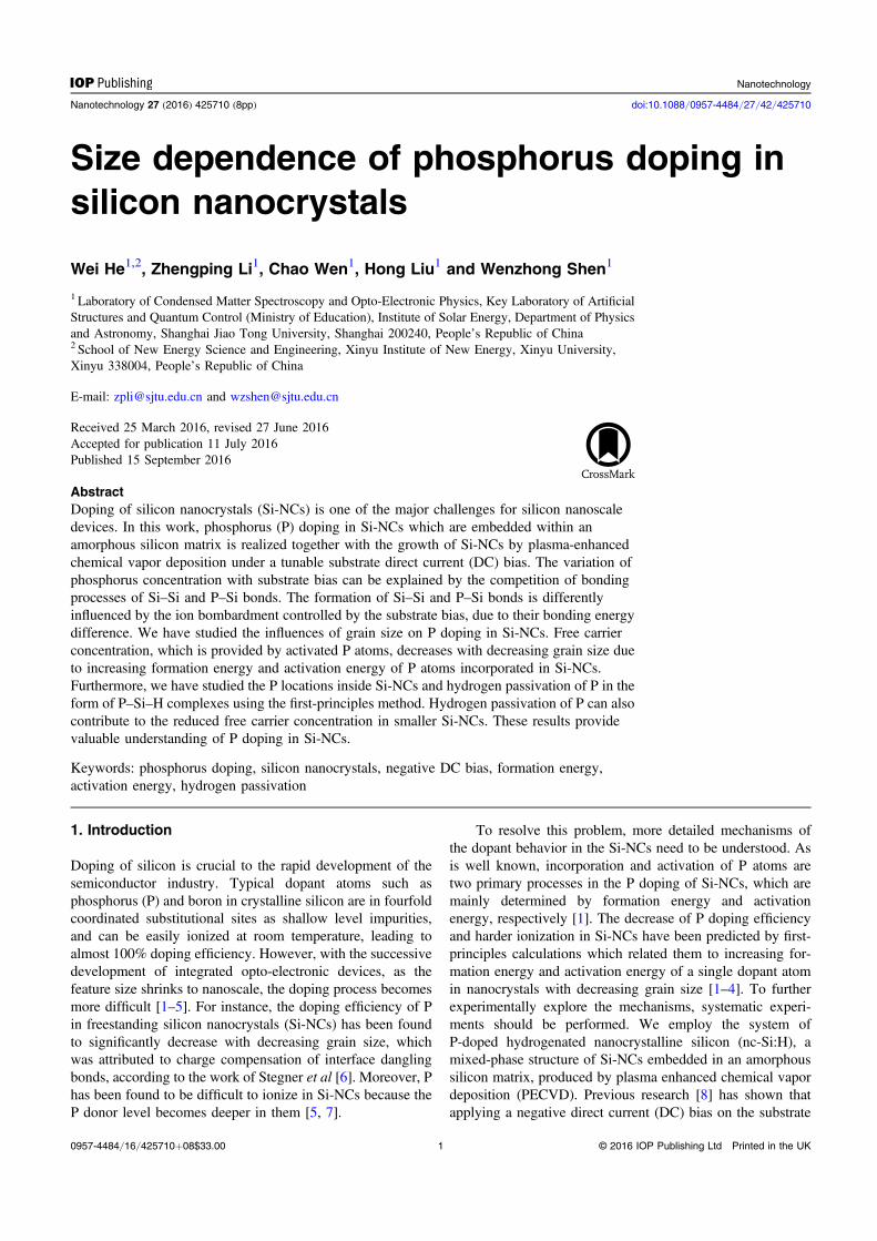
We performed XRD and Raman measurements to obtain thestructural properties of the nc-Si:H films prepared undervarious substrate DC biases. Figure 1(a) presents the XRDpattern of a typical sample under −100 V DC bias. The dif-fraction peaks at 2θ≈28.3°, 47.4° and 55.7° correspond to(111), (220) and (311) planes of crystalline silicon, respec-tively. The Si-NCs have shown preferential growth directionalong the (111) crystal orientation, as seen from figure 1(a)
2
Nanotechnology 27 (2016) 425710 W He et al

that the intensity of the (111) peak is the strongest andsharpest among the three peaks. Compared with crystallinesilicon, broadening of the three peaks indicates that the Si-NCs are embedded in an amorphous silicon matrix. Theaverage grain size d can be calculated from the (111) crystalorientation of the XRD pattern using the well-known Scherrerformula [21]: d=kλ/(βcosθ), where k=0.94 is a constant,λ=0.154 nm is the wavelength of the x-ray, β is the fullwidth at half-maximum of the diffraction peak, and θ is theBragg angle. Figure 1(b) shows the Raman spectrum of thesample under −100 V DC bias. The spectrum can bedecomposed into three independent Gaussian components[22, 23]: a narrow peak near 520 cm−1, which belongs to theasymmetric transverse optical mode of crystalline silicon, anintermediate mode of crystal-like phase around 506 cm−1
attributed to Si-Si bond dilation at grain boundaries, and abroad peak at 480 cm−1, which originates from the transverseoptical mode of amorphous silicon. Furthermore, the crys-talline volume fraction XC can be calculated from the formula[22, 23]: XC=(IC+IGB)/(IC+IGB+IA), where IC, IGBand IA represent integrated intensities of the crystalline phase,grain boundary phase and amorphous phase, respectively. Asshown in figure 1(c), it could be clearly seen that the grainsize d decreases from 5.6 nm to 3.6 nm when the DC biasincreases from 0 V to −200 V, then increases to 6.7 nm whenthe DC bias further increases to −300 V. The change of
crystalline volume fraction XC with DC bias is similar to thatof grain size, which is also depicted in figure 1(c). Figure 1(d)displays the optical transmission spectra for the sample under−100 V DC bias. According to Tauc’s linear extrapolationmethod [16, 17], the optical band gap Eg (1.96 eV) can bededuced from the following formula: (αhν)0.5=Ba
(hν−Eg), where α is absorption coefficient, hν is photonenergy and Ba is a constant, as shown in the inset offigure 1(d).
With the increasing DC bias, positive ionic species inplasmas gain a higher kinetic energy due to the acceleration ofthe DC electric field. In the initial increasing stage of the DCbias from 0 V to −200 V, more distorted chemical bonds areformed on the growing surface under bombardment of thepositive ionic species. Thus, amorphous phase content willincrease, corresponding to the decrease of grain size andcrystalline volume fraction, as illustrated in figure 1(c). It canbe ascribed to the ion bombardment-induced amorphization[10, 11] in the DC bias range. While further increasing theDC bias to −300 V, the H atoms and ions on the growingsurface are energetic enough to permeate into the subsurfaceand rearrange the amorphous silicon network structure. The Hatoms and ions insert into the strained Si-Si bonds, andsubsequent relaxation of the structure leads to the transfor-mation of amorphous silicon to nanocrystalline silicon.Therefore, the grain size and crystalline volume fraction
Figure 1. Structural and optical properties of a representative nc-Si:H sample under −100 V DC bias. (a) Experimental XRD spectrumshowing diffraction peaks (111), (220) and (311). (b) Experimental (open circles) and fitted Raman spectrum. (c) Average grain sizes d andcrystalline volume fractions XC of the samples under various DC biases. (d) Experimental optical transmission spectrum with Tauc-plotshown in the inset. Solid lines in (c) are a guide to the eye.
3
Nanotechnology 27 (2016) 425710 W He et al
increase due to the hydrogen-induced annealing effect[12, 13] in the DC bias range of −200∼−300 V, as shownin figure 1(c). In contrast to our previous study on intrinsic nc-Si:H films [8], the grain size and crystalline volume fractiondisplay a similar but more obvious change due to the addi-tional P-induced local deformation, which we will elucidatelater.
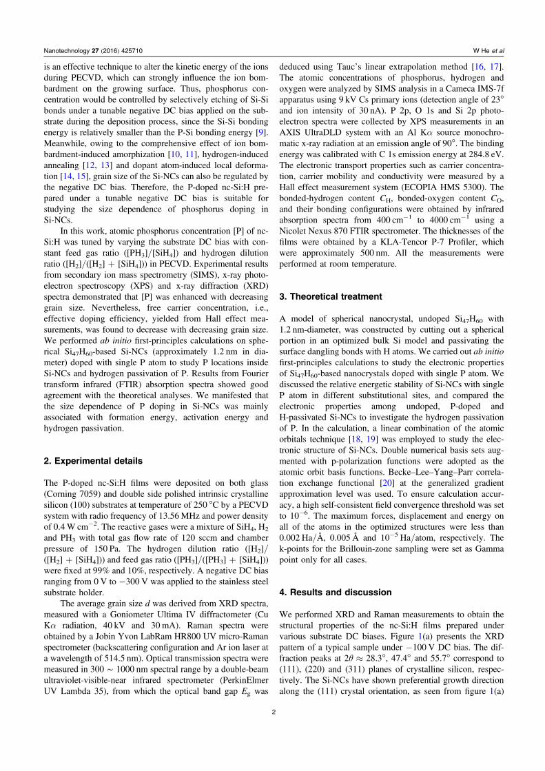
In order to study the elemental distribution in the nc-Si:Hfilms, we measure the phosphorus, hydrogen and oxygenconcentrations in the samples directly by SIMS. Figures 2(a)–(c) present the atomic concentrations of phosphorus [P],hydrogen [H] and oxygen [O] as a function of depth undervarious DC biases, respectively. We can see that the threeelements concentrations are nearly constant under each DCbias in the region of the plateau between 100 nm and 400 nm.Thus, we plot the three elements concentrations at the depthof 200 nm as a function of DC bias, as shown in figures 2(d)and (e). It can be seen that [P] increases as the DC biasincreases from 0 V to −200 V, and then decreases as the DCbias further increases to −300 V. There is a negative corre-lation between [H] and [O], which could be interpreted by thehydrogen passivation of dangling bonds [24]. Due to theincorporation of hydrogen atoms with the silicon danglingbonds located at grain boundaries, less oxygen atoms couldreside along grain boundaries in the form of Si–O bond.
There are two competing processes during which phos-phorus and silicon atoms are incorporated into nc-Si:H films.The first one is absorption of phosphorus and silicon atomsfrom the plasmas through bonding between radicals, mole-cules and growing surface. The second one is desorption ofphosphorus and silicon atoms from the growing surfacethrough etching of P–Si and Si–Si bonds. With the increasingDC bias, positive ionic species will gain a higher kineticenergy and bombard the growing surface more severely,
resulting in selectively etching of Si–Si bonds since the Si–Sibonding energy (321 kJ mol−1) is relatively smaller than theP–Si bonding energy (331 kJ mol−1) [9]. Under the bom-bardment of the positive ionic species, a part of kinetic energyof these species is transferred to P and Si atoms on thegrowing surface. Thus, the corresponding P–Si and Si–Sibonds will break more easily. In the initial increasing stage ofthe DC bias (0∼−200 V), P–Si and Si–Si bonds will beetched simultaneously, but more P–Si bonds will remain dueto the larger bonding energy, which can be evidenced by thefact that [P] increases obviously from 1.25×1021 cm−3 to3.71×1021 cm−3 in figure 2(d). However, further increasingthe DC bias to −300 V, kinetic energy of the positive ionicspecies is enhanced so much that P–Si bonds will also beetched severely. Consequently, [P] decreases to1.39×1021 cm−3, as shown in figure 2(d). It is worthwhile tonote that phosphorus concentration varies inversely with grainsize, as shown in figure 2(f). Since the P–Si bond is shorterthan the Si–Si bond [25], local deformation will be inducedby phosphorus incorporation. A higher phosphorus con-centration in the nc-Si:H films will reduce the tendencytoward crystallization, which is in agreement with previousobservation [15].
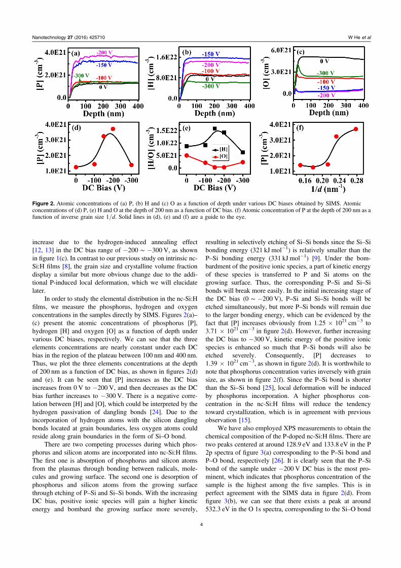
We have also employed XPS measurements to obtain thechemical composition of the P-doped nc-Si:H films. There aretwo peaks centered at around 128.9 eV and 133.8 eV in the P2p spectra of figure 3(a) corresponding to the P–Si bond andP–O bond, respectively [26]. It is clearly seen that the P–Sibond of the sample under −200 V DC bias is the most pro-minent, which indicates that phosphorus concentration of thesample is the highest among the five samples. This is inperfect agreement with the SIMS data in figure 2(d). Fromfigure 3(b), we can see that there exists a peak at around532.3 eV in the O 1s spectra, corresponding to the Si–O bond
Figure 2. Atomic concentrations of (a) P, (b) H and (c) O as a function of depth under various DC biases obtained by SIMS. Atomicconcentrations of (d) P, (e) H and O at the depth of 200 nm as a function of DC bias. (f) Atomic concentration of P at the depth of 200 nm as afunction of inverse grain size 1/d. Solid lines in (d), (e) and (f) are a guide to the eye.
4
Nanotechnology 27 (2016) 425710 W He et al
[27]. As shown in figure 3(c), the Si 2p spectra present twopeaks located at about 99.1 eV and 102.9 eV, correspondingto the Si0 state (Si–Si bond) and Si4+ state (Si–O bond),respectively [26, 28]. The intensity of the Si–O bonddecreases monotonously with increasing DC bias from 0 V to−300 V in both figures 3(b) and (c), indicating that oxygenconcentration on the surface decreases along with increasingDC bias. However, it is somewhat different from thatobtained by SIMS measurements in figure 2(e). The differ-ence may be related to the surface smoothness at the atomiclevel of the sample, i.e., a rough surface of the sample pro-duces more intermediate oxidation states [28]. The oxygenconcentration in the bulk is mainly influenced by hydrogenconcentration and hydrogen-related defect structure [24].
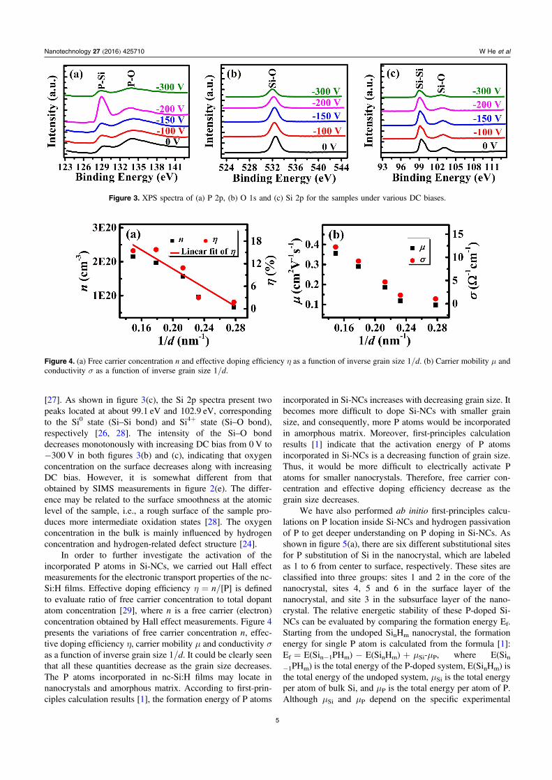
In order to further investigate the activation of theincorporated P atoms in Si-NCs, we carried out Hall effectmeasurements for the electronic transport properties of the nc-Si:H films. Effective doping efficiency η=n/[P] is definedto evaluate ratio of free carrier concentration to total dopantatom concentration [29], where n is a free carrier (electron)concentration obtained by Hall effect measurements. Figure 4presents the variations of free carrier concentration n, effec-tive doping efficiency η, carrier mobility μ and conductivity σ
as a function of inverse grain size 1/d. It could be clearly seenthat all these quantities decrease as the grain size decreases.The P atoms incorporated in nc-Si:H films may locate innanocrystals and amorphous matrix. According to first-prin-ciples calculation results [1], the formation energy of P atoms
incorporated in Si-NCs increases with decreasing grain size. Itbecomes more difficult to dope Si-NCs with smaller grainsize, and consequently, more P atoms would be incorporatedin amorphous matrix. Moreover, first-principles calculationresults [1] indicate that the activation energy of P atomsincorporated in Si-NCs is a decreasing function of grain size.Thus, it would be more difficult to electrically activate Patoms for smaller nanocrystals. Therefore, free carrier con-centration and effective doping efficiency decrease as thegrain size decreases.
We have also performed ab initio first-principles calcu-lations on P location inside Si-NCs and hydrogen passivationof P to get deeper understanding on P doping in Si-NCs. Asshown in figure 5(a), there are six different substitutional sitesfor P substitution of Si in the nanocrystal, which are labeledas 1 to 6 from center to surface, respectively. These sites areclassified into three groups: sites 1 and 2 in the core of thenanocrystal, sites 4, 5 and 6 in the surface layer of thenanocrystal, and site 3 in the subsurface layer of the nano-crystal. The relative energetic stability of these P-doped Si-NCs can be evaluated by comparing the formation energy Ef.Starting from the undoped SinHm nanocrystal, the formationenergy for single P atom is calculated from the formula [1]:Ef=E(Sin−1PHm)−E(SinHm)+μSi-μP, where E(Sin−1PHm) is the total energy of the P-doped system, E(SinHm) isthe total energy of the undoped system, μSi is the total energyper atom of bulk Si, and μP is the total energy per atom of P.Although μSi and μP depend on the specific experimental
Figure 3. XPS spectra of (a) P 2p, (b) O 1s and (c) Si 2p for the samples under various DC biases.
Figure 4. (a) Free carrier concentration n and effective doping efficiency η as a function of inverse grain size 1/d. (b) Carrier mobility μ andconductivity σ as a function of inverse grain size 1/d.
5
Nanotechnology 27 (2016) 425710 W He et al
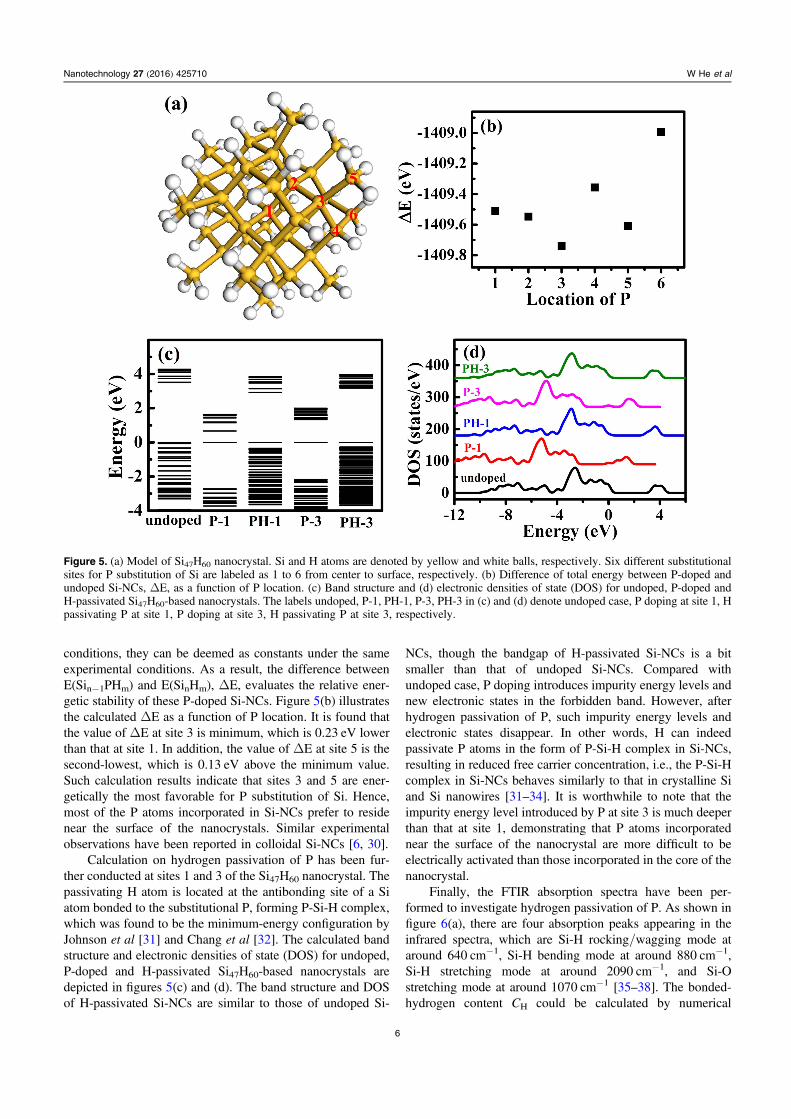
conditions, they can be deemed as constants under the sameexperimental conditions. As a result, the difference betweenE(Sin−1PHm) and E(SinHm), ΔE, evaluates the relative ener-getic stability of these P-doped Si-NCs. Figure 5(b) illustratesthe calculated ΔE as a function of P location. It is found thatthe value of ΔE at site 3 is minimum, which is 0.23 eV lowerthan that at site 1. In addition, the value of ΔE at site 5 is thesecond-lowest, which is 0.13 eV above the minimum value.Such calculation results indicate that sites 3 and 5 are ener-getically the most favorable for P substitution of Si. Hence,most of the P atoms incorporated in Si-NCs prefer to residenear the surface of the nanocrystals. Similar experimentalobservations have been reported in colloidal Si-NCs [6, 30].
Calculation on hydrogen passivation of P has been fur-ther conducted at sites 1 and 3 of the Si47H60 nanocrystal. Thepassivating H atom is located at the antibonding site of a Siatom bonded to the substitutional P, forming P-Si-H complex,which was found to be the minimum-energy configuration byJohnson et al [31] and Chang et al [32]. The calculated bandstructure and electronic densities of state (DOS) for undoped,P-doped and H-passivated Si47H60-based nanocrystals aredepicted in figures 5(c) and (d). The band structure and DOSof H-passivated Si-NCs are similar to those of undoped Si-
NCs, though the bandgap of H-passivated Si-NCs is a bitsmaller than that of undoped Si-NCs. Compared withundoped case, P doping introduces impurity energy levels andnew electronic states in the forbidden band. However, afterhydrogen passivation of P, such impurity energy levels andelectronic states disappear. In other words, H can indeedpassivate P atoms in the form of P-Si-H complex in Si-NCs,resulting in reduced free carrier concentration, i.e., the P-Si-Hcomplex in Si-NCs behaves similarly to that in crystalline Siand Si nanowires [31–34]. It is worthwhile to note that theimpurity energy level introduced by P at site 3 is much deeperthan that at site 1, demonstrating that P atoms incorporatednear the surface of the nanocrystal are more difficult to beelectrically activated than those incorporated in the core of thenanocrystal.
Finally, the FTIR absorption spectra have been per-formed to investigate hydrogen passivation of P. As shown infigure 6(a), there are four absorption peaks appearing in theinfrared spectra, which are Si-H rocking/wagging mode ataround 640 cm−1, Si-H bending mode at around 880 cm−1,Si-H stretching mode at around 2090 cm−1, and Si-Ostretching mode at around 1070 cm−1 [35–38]. The bonded-hydrogen content CH could be calculated by numerical
Figure 5. (a) Model of Si47H60 nanocrystal. Si and H atoms are denoted by yellow and white balls, respectively. Six different substitutionalsites for P substitution of Si are labeled as 1 to 6 from center to surface, respectively. (b) Difference of total energy between P-doped andundoped Si-NCs, ΔE, as a function of P location. (c) Band structure and (d) electronic densities of state (DOS) for undoped, P-doped andH-passivated Si47H60-based nanocrystals. The labels undoped, P-1, PH-1, P-3, PH-3 in (c) and (d) denote undoped case, P doping at site 1, Hpassivating P at site 1, P doping at site 3, H passivating P at site 3, respectively.
6
Nanotechnology 27 (2016) 425710 W He et al

integration of the Si-H rocking/wagging mode at around
640 cm−1 using the equation [35, 36]: òa nn
n= wCA
Nd ,H
Si
( )
where ν is the wave number, α(ν) is the absorption coeffi-cient, Aω=2.1×1019 cm−2 is the proportionality constant[35], NSi=5×1022 cm−3 is the atomic density of crystal-line silicon. Analogously, the bonded-oxygen content CO
could be obtained by numerical integration of the Si-Ostretching mode at around 1070 cm−1 withAω=2.8×1019 cm−2 [37, 38]. The variations of CH and CO
with increasing DC bias have been demonstrated infigure 6(b). We can see that CH increases as the DC biasincreases from 0 V to −200 V, and then decreases as the DCbias further increases to −300 V. On the contrary, CO showsan inverse evolution compared with CH, which is in goodagreement with the SIMS results in figure 2(e). It is worthnoting that there is a strong positive correlation between CH
and [P] by contrasting figure 6(b) with figure 2(d). It could beexplained by the increasing hydrogen passivation of Si dan-gling bonds in amorphous matrix [39, 40] and P atoms in Si-NCs. Along with shrinking grain size accompanied withincreasing P concentration, more P atoms are incorporatednear the surface of the Si-NCs, which are more likely to bepassivated by H atoms.
5. Conclusions
P-doped nc-Si:H has been prepared by the PECVD method,applying a tunable substrate DC bias in the range of0∼−300 V. Phosphorus concentration and grain size of theSi-NCs were regulated by the substrate DC bias simulta-neously, offering an appropriate way to study the sizedependence of phosphorus doping in Si-NCs. Phosphorusconcentration was mainly associated with ion bombardmentcontrolled by the substrate DC bias and the difference ofbonding energy between the Si-Si bond and P-Si bond.Experimental results demonstrated that grain size variedinversely with phosphorus concentration. Free carrier
concentration provided by activated P atoms declined withdecreasing grain size. Free carrier concentration dependsprimarily on the formation energy and activation energy of Patoms incorporated in Si-NCs that both increase withdecreasing grain size. Furthermore, our first-principles cal-culations manifest that most of the P atoms incorporated in Si-NCs prefer to reside near the surface of the Si-NCs and Hatoms could passivate P atoms in the form of P-Si-H complex.Hence, the effective doping efficiency of P atoms incorpo-rated in Si-NCs is mainly associated with formation energy,activation energy and hydrogen passivation.
Acknowledgments
This work was supported by the National Natural ScienceFoundation of China (61234005, 11474201 and 11674225).Wei He would like to thank Dr Limin Sun from InstrumentalAnalysis Center of Shanghai Jiao Tong University for XPSmeasurements and Prof Fanying Meng from Shanghai Insti-tute of Microsystem and Information Technology, ChineseAcademy of Sciences, for Hall effect measurements.
References
[1] Cantele G, Degoli E, Luppi E, Magri R, Ninno D,Iadonisi G and Ossicini S 2005 First-principles study of n-and p-doped silicon nanoclusters Phys. Rev. B 72 113303
[2] Dalpian G M and Chelikowsky J R 2006 Self-purification insemiconductor nanocrystals Phys. Rev. Lett. 96 226802
[3] Chan T L, Tiago M L, Kaxiras E and Chelikowsky J R 2008Size limits on doping phosphorus into silicon nanocrystalsNano Lett. 8 596–600
[4] Melnikov D V and Chelikowsky J R 2004 Quantumconfinement in phosphorus-doped silicon nanocrystals Phys.Rev. Lett. 92 046802
[5] König D, Gutsch S, Gnaser H, Wahl M, Kopnarski M,Göttlicher J, Steininger R, Zacharias M and Hiller D 2015Location and electronic nature of phosphorus in the Sinanocrystal−SiO2 system Sci. Rep. 5 09702
Figure 6. (a) Infrared absorption spectra of nc-Si:H films under various DC biases. (b) Hydrogen and oxygen content of the nc-Si:H filmsunder different DC voltages. Solid lines in (b) are a guide for the eye.
7
Nanotechnology 27 (2016) 425710 W He et al
[6] Stegner A R, Pereira R N, Lechner R, Klein K, Wiggers H,Stutzmann M and Brandt M S 2009 Doping efficiency infreestanding silicon nanocrystals from the gas phase:phosphorus incorporation and defect-induced compensationPhys. Rev. B 80 165326
[7] Sumida K, Ninomiya K, Fujii M, Fujio K and Hayashi S 2007Electron spin-resonance studies of conduction electrons inphosphorus-doped silicon nanocrystals J. Appl. Phys. 101033504
[8] Wen C, Xu H, Liu H, Li Z P and Shen W Z 2013 Passivationof nanocrystalline silicon photovoltaic materials employinga negative substrate bias Nanotechnology 24 455602
[9] Lide D R 2010 CRC Handbook of Chemistry and Physics 90thedn (Boca Raton, FL: CRC Press/Taylor and Francis)
[10] Hamers E A G, Fontcuberta I Morral A, Niikura C,Brenot R and Roca I Cabarrocas P 2000 Contribution of ionsto the growth of amorphous, polymorphous, andmicrocrystalline silicon thin films J. Appl. Phys. 88 3674–88
[11] Kalache B, Kosarev A I, Vanderhaghen R andRoca I Cabarrocas P 2003 Ion bombardment effects onmicrocrystalline silicon growth mechanisms and on the filmproperties J. Appl. Phys. 93 1262–73
[12] Nakamura K, Yoshino K, Takeoka S and Shimizu I 1995 Rolesof atomic hydrogen in chemical annealing Jpn. J. Appl.Phys. 34 442–9
[13] Sriraman S, Agarwal S, Aydil E S and Maroudas D 2002Mechanism of hydrogen-induced crystallization ofamorphous silicon Nature 418 62–5
[14] Hao X J, Cho E-C, Flynn C, Shen Y S, Conibeer G andGreen M A 2008 Effects of boron doping on the structuraland optical properties of silicon nanocrystals in a silicondioxide matrix Nanotechnology 19 424019
[15] Alpuim P, Chu V and Conde J P 2003 Electronic and structuralproperties of doped amorphous and nanocrystalline silicondeposited at low substrate temperatures by radio-frequencyplasma-enhanced chemical vapor deposition J. Vac. Sci.Technol. A 21 1048–54
[16] Chen H, Gullanar M H and Shen W Z 2004 Effects of highhydrogen dilution on the optical and electrical properties inB-doped nc-Si:H thin films J. Cryst. Growth 260 91–101
[17] Tauc J, Grigorovici R and Vancu A 1966 Optical propertiesand electronic structure of amorphous germanium Phys.Stat. Sol. 15 627–37
[18] Delley B 1990 An all electron numerical method for solvingthe local density functional for polyatomic moleculesJ. Chem. Phys. 92 508–17
[19] Delley B 1990 From molecules to solids with the DMol3
approach 2000 J. Chem. Phys. 113 7756–64[20] Lee C, Yang W and Parr R G 1988 Development of the Colic-
Salvetti correlation-energy formula into a functional of theelectron density Phys. Rev. B 37 785–9
[21] Fitzsimmons M R, Eastman J A, Muller-Stach M andWallner G 1991 Structural characterization of nanometer-sized crystalline Pd by x-ray-diffraction techniques Phys.Rev. B 44 2452–60
[22] Bustarret E, Hachicha M A and Brunel M 1988 Experimentaldetermination of the nanocrystalline volume fraction insilicon thin films from Raman spectroscopy Appl. Phys. Lett.52 1675–7
[23] Droz C, Vallat-Sauvain E, Bailat J, Feitknecht L, Meier J andShah A 2004 Relationship between Raman crystallinity and
open-circuit voltage in microcrystalline silicon solar cellsSol. Energy Mater. Sol. Cells 81 61–71
[24] Wen C, Xu H, He W, Li Z P and Shen W Z 2014 Tuningoxygen impurities and microstructure of nanocrystallinesilicon photovoltaic materials through hydrogen dilutionNanoscale Res. Lett. 9 303
[25] Wang Y J, Chen X X and Hamers R J 1994 Atomic-resolutionstudy of overlayer formation and interfacial mixing in theinteraction of phosphorus with Si(001) Phys. Rev. B 504534–47
[26] Perego M, Bonafos C and Fanciulli M 2010 Phosphorusdoping of ultra-small silicon nanocrystals Nanotechnology21 025602
[27] Jo M H, Park H H, Kim D J, Hyun S H, Choi S Y and Paik J T1997 SiO2 aerogel film as a novel intermetal dielectricJ. Appl. Phys. 82 1299–304
[28] Himpsel F J, McFeely F R, Taleb-Ibrahimi A, Yarmoff J A andHollinger G 1988 Microscopic structure of the SiO2/Siinterface Phys. Rev. B 38 6084–96
[29] Kumar P and Schroeder B 2008 Electrical properties/dopingefficiency of doped microcrystalline silicon layers preparedby hot-wire chemical vapor deposition Thin Solid Films 516580–3
[30] Pi X D, Gresback R, Liptak R W, Campbell S A andKortshagen U 2008 Doping efficiency, dopant location,and oxidation of Si nanocrystals Appl. Phys. Lett. 92123102
[31] Johnson N M, Herring C and Chadi D J 1986 Interstitialhydrogen and neutralization of shallow-donor impurities insingle-crystal silicon Phys. Rev. Lett. 56 769–72
[32] Chang K J and Chadi D J 1988 Theory of hydrogen passivationof shallow-level dopants in crystalline silicon Phys. Rev.Lett. 60 1422–5
[33] Fukata N, Sato S, Morihiro H, Murakami K, Ishioka K,Kitajima M and Hishita S 2007 Dopant dependence onpassivation and reactivation of carrier after hydrogenationJ. Appl. Phys. 101 046107
[34] Fukata N, Chen J, Sekiguchi T, Matsushita S, Oshima T,Uchida N, Murakami K, Tsurui T and Ito S 2007Phosphorus doping and hydrogen passivation of donors anddefects in silicon nanowires synthesized by laser ablationAppl. Phys. Lett. 90 153117
[35] Langford A A, Fleet M L, Nelson B P, Lanford W A andMaley N 1992 Infrared absorption strength and hydrogencontent of hydrogenated amorphous silicon Phys. Rev. B 4513367–77
[36] Kroll U, Meier J, Shah A, Mikhailov S and Weber J 1996Hydrogen in amorphous and microcrystalline siliconfilms prepared by hydrogen dilution J. Appl. Phys. 804971–5
[37] Lucovsky G, Nemanich R J and Knights J C 1979 Structuralinterpretation of the vibrational spectra of a-Si:H alloysPhys. Rev. B 19 2064–73
[38] Freeman E C and Paul W 1978 Infrared vibrational spectra ofrf-sputtered hydrogenated amorphous silicon Phys. Rev. B18 4288–300
[39] Fedders P A 1998 Theory of phosphorus doping in a-Si:HPhys. Rev. B 58 7020–3
[40] Pandey A, Cai B, Podraza N and Drabold D A 2014 Electricalactivity of boron and phosphorus in hydrogenatedamorphous silicon Phys. Rev. Applied 2 054005
8
Nanotechnology 27 (2016) 425710 W He et al