electricity theft control using gsm and emic · electricity theft control using gsm ... of...
TRANSCRIPT
ELECTRICITY THEFTCONTROL USING GSM AND
EMIC
ABSTRACTElectrical energy is very imperative for ever day life and a spine for the
industry. Electricity is indiscipline to our daily life with increasing need
of electricity the power theft is also increasing power theft is a problem
that continues to plague power sector across the whole country the
objective of this project is to design a system in order to avoid the
displeasure for the users from theft bill irrespective of the use of the
electricity due to theft using GSM module. In order to integrate the
1
various parts together we must first properly understand the working of
the different parts to be integrated together. A brief study is alone on the
components and the technology which we are going to use in our project.
TABLE OF CONTENTSCHAPTER NO TITLE PAGE NO ABSTRACT 2
1 INTRODUCTION 1.1 OVERVIEW OF THE PROJECT 6 1.2 BLOCK DIAGRAM 72 HARDWARE AND SOFTWARE DESCRIPTION
2.1 HARDWARE DESCRIPTION
2.1.1 ARM 7 (LPC2148) PROCESSOR 10
2.1.2 BUZZER 13
2.1.3 POWER SUPPLY UNIT 15
2.1.4 LCD DISPLAY (2*16 DISPLAY) 16
2.1.5 RELAY 20
2.1.6 GSM MODULE 25
2.1.7 RS 232 CABLE 28
2 .18 MAX232 IC2 30
2

2.1.9 EMIC 32
2.2 SOFTWARE DESCRIPTON
2.2.1 KEIL COMPILER 34
3 CIRCUT DIAGRAM 36 4 EMIC MODULE 38 5 PROGRAMS 39 5.1 PROGRAMS LOADED IN ARM7 6 APPLICATIONS 40 7 CONCLUSION 43 8 REFERENCES 44
3

CHAPTER 1
INTRODUCTION
1.1 OVERVIEW OF THE PROJECT To identify the theft of electricity from
transmission lines or from home distribution. None to monitor the over
load of usage at end user.No automatic update of load consumption
details to authority.Not reliable and robust. Electricity monitoring system
using sensors.Microcontroller based authentication.Well protected and
robust system .High-quality speech synthesis for English and Spanish
languages.Nine pre-defined voice styles comprising male, female, and
child.On-board audio power amplifier and 1/8” (3.5 mm) audio
jack.UART interfacable at 9600bps . Reading Internet-based data streams
(such as e-mails or Twitter feeds).Conveying status or sensor results from
robots, scientific equipment, or industrial machinery.Language learning
or speech aids for educational environments. order to avoid the
displeasure for the users from theft bill irrespective of the use of the
4
electricity due to theft using GSM module. In order to integrate the
various parts together we must first properly understand the working of
the different parts to be integrated together. A brief study is alone on the
components and the technology which we are going to use in our project.
1.2 BLOCK DIAGRAM
5
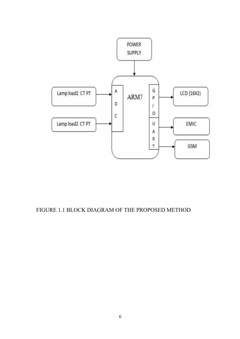
FIGURE 1.1 BLOCK DIAGRAM OF THE PROPOSED METHOD
6

CHAPTER 2
HARDWARE AND SOFTWARE DESCRIPTION
The proposed system requires the following components,
2.1 HARDWARE DESCRIPTION
1. ARM 7 (LPC2148) PROCESSOR
2. BUZZER
7
3. POWER SUPPLY UNIT
4. LCD DISPLAY (2*16 DISPLAY)
5. RELAY
6. GSM MODULE
7. RS 232 CABLE
8. MAX232 IC
9. EMIC
2.2 SOFTWARE DESCRIPTON
1. KEIL COMPILER
2.1.1 ARM 7 (LPC2148) PROCESSOR
8
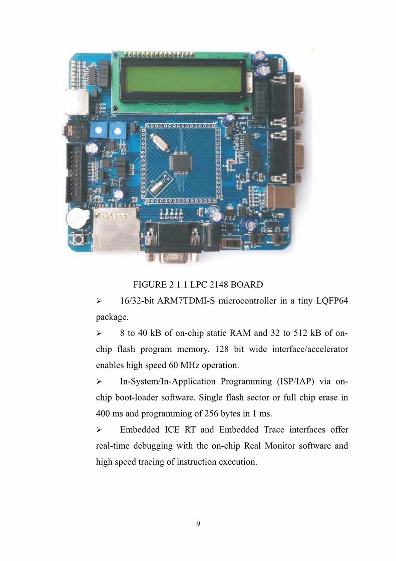
FIGURE 2.1.1 LPC 2148 BOARD
16/32-bit ARM7TDMI-S microcontroller in a tiny LQFP64
package.
8 to 40 kB of on-chip static RAM and 32 to 512 kB of on-
chip flash program memory. 128 bit wide interface/accelerator
enables high speed 60 MHz operation.
In-System/In-Application Programming (ISP/IAP) via on-
chip boot-loader software. Single flash sector or full chip erase in
400 ms and programming of 256 bytes in 1 ms.
Embedded ICE RT and Embedded Trace interfaces offer
real-time debugging with the on-chip Real Monitor software and
high speed tracing of instruction execution.
9
One or two (LPC2141/2 vs. LPC2144/6/8) 10-bit A/D
converters provide a total of 6/14 analog inputs, with conversion
times as low as 2.44 μs per channel.
Single 10-bit D/A converter provides variable analog output.
Two 32-bit timers/external event counters (with four capture
and four compare channels each), PWM unit (six outputs) and
watchdog.
Low power real-time clock with independent power and
dedicated 32 kHz clock input.
Multiple serial interfaces including two UARTs (16C550),
two Fast I2C-bus (400 kbit/s), SPI and SSP with buffering and
variable data length capabilities.
Vectored interrupt controller with configurable priorities and
vector addresses.
Up to 45 of 5 V tolerant fast general purpose I/O pins in a
tiny LQFP64 package.
Up to nine edge or level sensitive external interrupt pins
available.
60 MHz maximum CPU clock available from programmable
on-chip PLL with settling time of 100 μs.
The ARM7TDMI-S is a general function purpose 32-bit data register
processor, which provides great efficeiency and very small voltage
consumption. The ARM design is based on Reduced Instruction Set Computer
(RISC) method, and the opcode set and relevant decode procedure are much
easier than those of micro code Complex Instruction Set systems. This
simplicity results yielded in a big instruction throughput and impressive real-
time interrupt reply from a low and economical processor core. Pipeline
10
enhanced methods are deployed so that all parts of the carry out and storage
systems can function recursively. Typically, while single instruction is being
executed, their follower is being decoded, and a third instruction is being given
to memory. The ARM7TDMI-S processor also employs a specific architectural
plan known as THUMB, which makes it specifically suited to high-bulk
applications with memory limitations, or applications where software density is
an problem. The key theme behind THUMB is that of a great super-reduced
assembly code set. Essentially, the ARM7TDMI-S supports two instruction sets:
The ARM7TDMI-S processor also employs a specific architectural plan known
as THUMB, which makes it specifically suited to high-bulk applications with
memory limitations, or applications where software density is an problem. The
key theme behind THUMB is that of a great super-reduced assembly code set.
Essentially, the ARM7TDMI-S supports two instruction sets:
The standard 32-bit ARM instruction set.
A 16-bit THUMB instruction set.
The THUMB set’s 16-bit instruction length allows it to towards twice the
density of defined ARM program while regaining most of the controller
performance advantage over a common 16-bit processor using 16-bit function
registers. This is feasible because THUMB program executes on the similar 32-
bit register set as ARM program. THUMB program is able to give up to 65% of
the software size of pre-processor, and 160% of the performance of an
equivalent ARM processor related to a 16-bit storage system. The ARM7TDMI-
S controller is described in brief in the ARM7TDMI-S Datasheet that can be
found on official ARM website. This is feasible because THUMB program
executes on the similar 32-bit register set as ARM program. THUMB program
is able to give up to 65% of the software size of preprocessor and 160% of the
performance of an equivalent ARM processor related to a 16-bit storage system.
11
The THUMB set’s 16-bit instruction length allows it to towards twice the
density of defined ARM program while regaining most of the controller
performance advantage over a common 16-bit processor using 16-bit function
registers. This is feasible because THUMB program executes on the similar 32-
bit register set as ARM program.
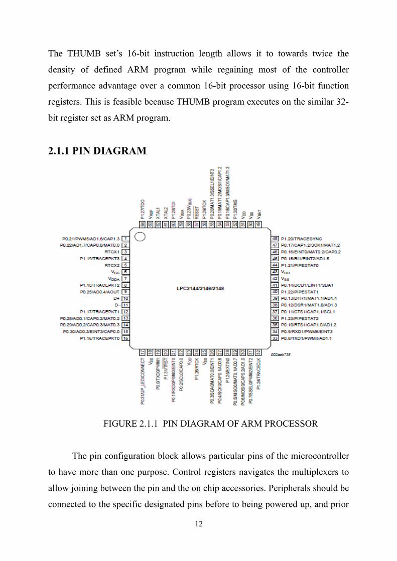
2.1.1 PIN DIAGRAM
FIGURE 2.1.1 PIN DIAGRAM OF ARM PROCESSOR
The pin configuration block allows particular pins of the microcontroller
to have more than one purpose. Control registers navigates the multiplexers to
allow joining between the pin and the on chip accessories. Peripherals should be
connected to the specific designated pins before to being powered up, and prior
12

to any related interrupt(s) being enabled. Selection of a specific function on a
port I/O completely excludes all other true purpose else present on the same I/O.
The only partial exception from the above protocol of exclusion is the case of
inputs to the A/D module. Regardless of the purpose that is selected for the port
I/O that also hosts the A/D I/P, this A/D input can be noted at any time and
difference of the potential values on this pin will be recollected in the A/D
monitoring registers. The only partial exception from the above protocol of
exclusion is the case of inputs to the A/D module. Regardless of the purpose
that is selected for the port I/O that also hosts the A/D I/P, this A/D input can be
noted at any time and difference of the potential values on this pin will be
recollected in the A/D monitoring registers.
Peripherals should be connected to the specific designated pins before to being
powered up, and prior to any related interrupt(s) being enabled. Selection of a
specific function on a port I/O completely excludes all other true purpose else
present on the same I/O. The only partial exception from the above protocol of
exclusion is the case of inputs to the A/D module. Not concern of the purpose
that is specific for the port I/O that also hosts the A/D I/P, this A/D input can be
noted at any time and difference of the potential values on this pin will be
recollected in the A/D modules.
However, true analog values (s) can be gathered if and only if the function of an
analog input is selected. Only in this situation proper interface circuit is in
powered state in between the physical pin and the A/D module
13
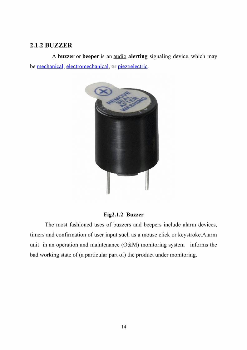
2.1.2 BUZZER
A buzzer or beeper is an audio alerting signaling device, which may
be mechanical, electromechanical, or piezoelectric.
Fig2.1.2 Buzzer
The most fashioned uses of buzzers and beepers include alarm devices,
timers and confirmation of user input such as a mouse click or keystroke.Alarm
unit in an operation and maintenance (O&M) monitoring system informs the
bad working state of (a particular part of) the product under monitoring.
14
2.1.3 POWER SUPPLY UNIT
CIRCUIT DIAGRAM
Fig.2.1.3 Circuit Diagram of Power Supply
WORKING PRINCIPLE
The AC voltage, typically 220V rms, is connected to a transformer, which
steps that ac voltage down to the level of the desired DC output. A diode
rectifier then provides a full-wave rectified voltage that is initially filtered by a
simple capacitor filter to produce a dc voltage. This resulting dc voltage usually
has some ripple or ac voltage variation.
A regulator circuit removes the ripples and also remains the same dc value
even if the input dc voltage varies, or the load connected to the output dc
voltage changes.
Fig 2.1.4 Block diagram of power supply
TRANSFORMER
The potential transformer will step down the power supply voltage (0-230V)
to (0-6V) level. Then the secondary of the potential transformer will be
connected to the precision rectifier, which is constructed with the help of op–
amp. The advantages of using precision rectifier are it will give peak voltage
output as DC; rest of the circuits will give only RMS output.
BRIDGE RECTIFIER
15
When four diodes are connected as shown in figure, the circuit is called as
bridge rectifier. The input to the circuit is applied to the diagonally opposite
corners of the network, and the output is taken from the remaining two corners.
Let us assume that the transformer is working properly and there is a positive
potential, at point A and a negative potential at point B. the positive potential at
point A will forward bias D3 and reverse bias D4.
The negative potential at point B will forward bias D1 and reverse D2. At
this time D3 and D1 are forward biased and will allow current flow to pass
through them; D4 and D2 are reverse biased and will block current flow.
The path for current flow is from point B through D1, up through RL,
through D3, through the secondary of the transformer back to point B. this path
is indicated by the solid arrows. Waveforms (1) and (2) can be observed across
D1 and D3.
One-half cycle later the polarity across the secondary of the transformer
reverse, forward biasing 2 and D4 and reverse biasing D1 and D3. Current flow
will now be from point A through D4, up through RL, through D2, through the
secondary of T1, and back to point A. This path is indicated by the broken
arrows. Waveforms (3) and (4) can be observed across D2 and D4. The current
flow through RL is always in the same direction. In flowing through RL this
current develops a voltage corresponding to that shown waveform (5). Since
current flows through the load (RL) during both half cycles of the applied
voltage, this bridge rectifier is a full-wave rectifier.
One advantage of a bridge rectifier over a conventional full-wave rectifier is
that with a given transformer the bridge rectifier produces a voltage output that
is nearly twice that of the conventional full-wave circuit.
16
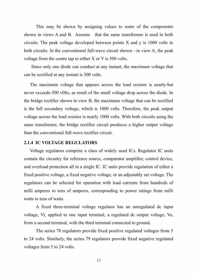
This may be shown by assigning values to some of the components
shown in views A and B. Assume that the same transformer is used in both
circuits. The peak voltage developed between points X and y is 1000 volts in
both circuits. In the conventional full-wave circuit shown—in view A, the peak
voltage from the centre tap to either X or Y is 500 volts.
Since only one diode can conduct at any instant, the maximum voltage that
can be rectified at any instant is 500 volts.
The maximum voltage that appears across the load resistor is nearly-but
never exceeds-500 v0lts, as result of the small voltage drop across the diode. In
the bridge rectifier shown in view B, the maximum voltage that can be rectified
is the full secondary voltage, which is 1000 volts. Therefore, the peak output
voltage across the load resistor is nearly 1000 volts. With both circuits using the
same transformer, the bridge rectifier circuit produces a higher output voltage
than the conventional full-wave rectifier circuit.
2.1.4 IC VOLTAGE REGULATORS
Voltage regulators comprise a class of widely used ICs. Regulator IC units
contain the circuitry for reference source, comparator amplifier, control device,
and overload protection all in a single IC. IC units provide regulation of either a
fixed positive voltage, a fixed negative voltage, or an adjustably set voltage. The
regulators can be selected for operation with load currents from hundreds of
milli amperes to tens of amperes, corresponding to power ratings from milli
watts to tens of watts.
A fixed three-terminal voltage regulator has an unregulated dc input
voltage, Vi, applied to one input terminal, a regulated dc output voltage, Vo,
from a second terminal, with the third terminal connected to ground.
The series 78 regulators provide fixed positive regulated voltages from 5
to 24 volts. Similarly, the series 79 regulators provide fixed negative regulated
voltages from 5 to 24 volts.
17
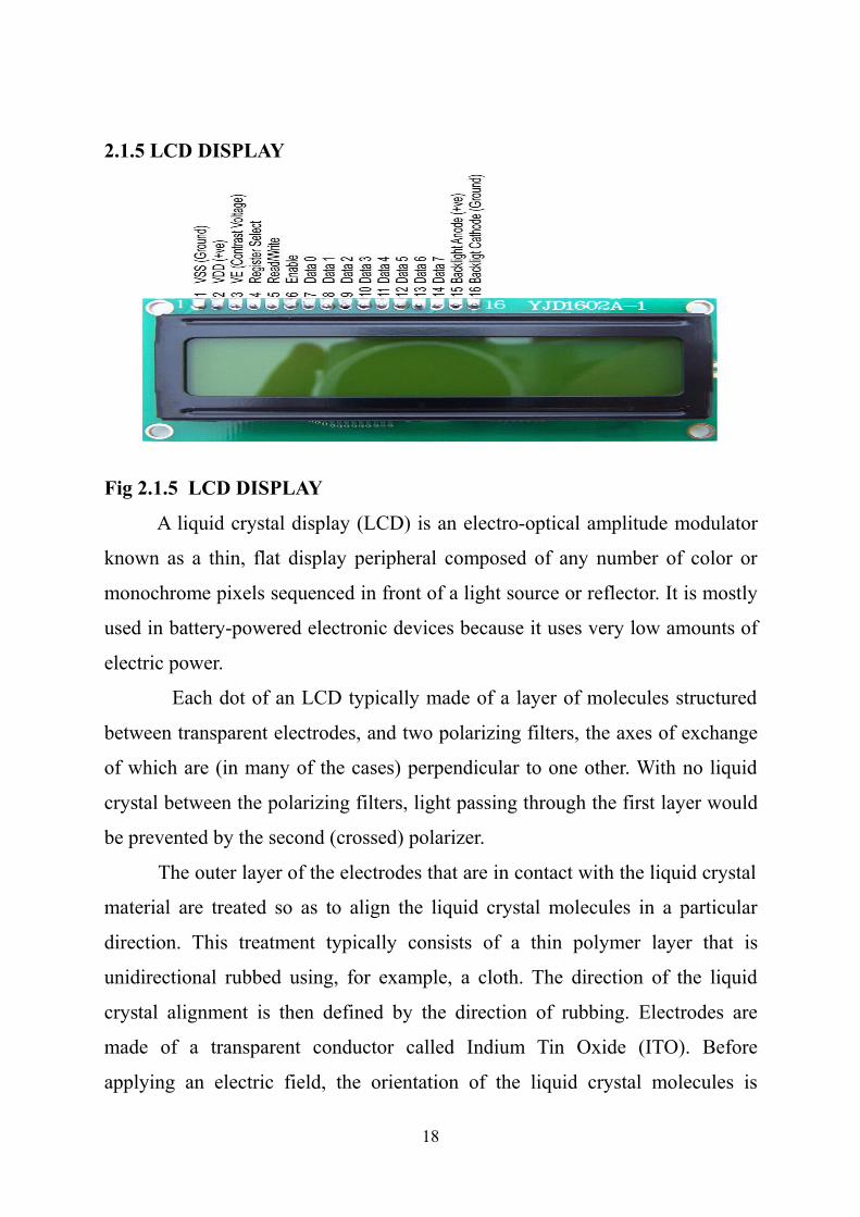
2.1.5 LCD DISPLAY
Fig 2.1.5 LCD DISPLAY
A liquid crystal display (LCD) is an electro-optical amplitude modulator
known as a thin, flat display peripheral composed of any number of color or
monochrome pixels sequenced in front of a light source or reflector. It is mostly
used in battery-powered electronic devices because it uses very low amounts of
electric power.
Each dot of an LCD typically made of a layer of molecules structured
between transparent electrodes, and two polarizing filters, the axes of exchange
of which are (in many of the cases) perpendicular to one other. With no liquid
crystal between the polarizing filters, light passing through the first layer would
be prevented by the second (crossed) polarizer.
The outer layer of the electrodes that are in contact with the liquid crystal
material are treated so as to align the liquid crystal molecules in a particular
direction. This treatment typically consists of a thin polymer layer that is
unidirectional rubbed using, for example, a cloth. The direction of the liquid
crystal alignment is then defined by the direction of rubbing. Electrodes are
made of a transparent conductor called Indium Tin Oxide (ITO). Before
applying an electric field, the orientation of the liquid crystal molecules is
18
determined by the alignment at the surfaces. In a twisted nematic device, the
surface alignment directions at the two electrodes are perpendicular to each
other, and so the molecules arrange themselves in a helical structure, or twist.
Because the liquid crystal material is birefringent, light passing through one
polarizing filter is rotated by the liquid crystal helix as it passes through the
liquid crystal layer, allowing it to pass through the second polarized filter. Half
of the incident light is absorbed by the first polarizing filter, but otherwise the
entire assembly is reasonably transparent.
When a voltage is applied across the electrodes, a torque acts to align the
liquid crystal molecules parallel to the electric field, distorting the helical
structure (this is resisted by elastic forces since the molecules are constrained at
the surfaces). This reduces the rotation of the polarization of the incident light,
and the device appears grey. If the applied voltage is large enough, the liquid
crystal molecules in the center of the layer are almost completely untwisted and
the polarization of the incident light is not rotated as it passes through the liquid
crystal layer. This light will then be mainly polarized perpendicular to the
second filter, and thus be blocked and the pixel will appear black. By controlling
the voltage applied across the liquid crystal layer in each pixel, light can be
allowed to pass through in varying amounts thus constituting different levels of
gray.
The optical effect of a twisted nematic device in the voltage-on state is far less
dependent on variations in the device thickness than that in the voltage-off state.
Because of this, these devices are usually operated between crossed polarizers
such that they appear bright with no voltage (the eye is much more sensitive to
variations in the dark state than the bright state). These devices can also be
operated between parallel polarizers, in which case the bright and dark states are
reversed. The voltage-off dark state in this configuration appears blotchy,
however, because of small variations of thickness across the device.
LCD pin descriptions:
19
The LCD discussed in this section has 14 pins. The function of each pin is
given in the table below.
VCC, VSS, and VEE:
While VCC and VSS provide +5V and ground, respectively, VEE is used for
controlling LCD contrast.
RS, Register Select:
There are two very important registers inside the LCD. The RS pin is used
for their selection as follows. If RS=0, the instruction command code register is
selected, allowing the user to send a command such as clear display, cursor at
home, etc. If RS=1 the data register is selected, allowing the user to send data to
be displayed on the LCD.
R/W, Read/Write:
R/W input allows the user to write information to the LCD or read
information from it. R/W=1 when reading; R/W=0 when writing.
E, Enable:
The enable pin is used by the LCD to latch information presented to its
data pins. When data is supplied to data pins, a high-to-low pulse must be
applied to this pin in order for the LCD to latch in the data present at the data
pins. This pulse must be a minimum of 450ns wide.
D0-D7:
The 8-bit data pins, D0-D7, are used to send information to the LCD or
read the contents of the LCD’s internal registers.
To display letters and numbers, we send ASCII codes for the letters A-Z,
a-z, and numbers 0-9 to these pins while making RS=1.
20
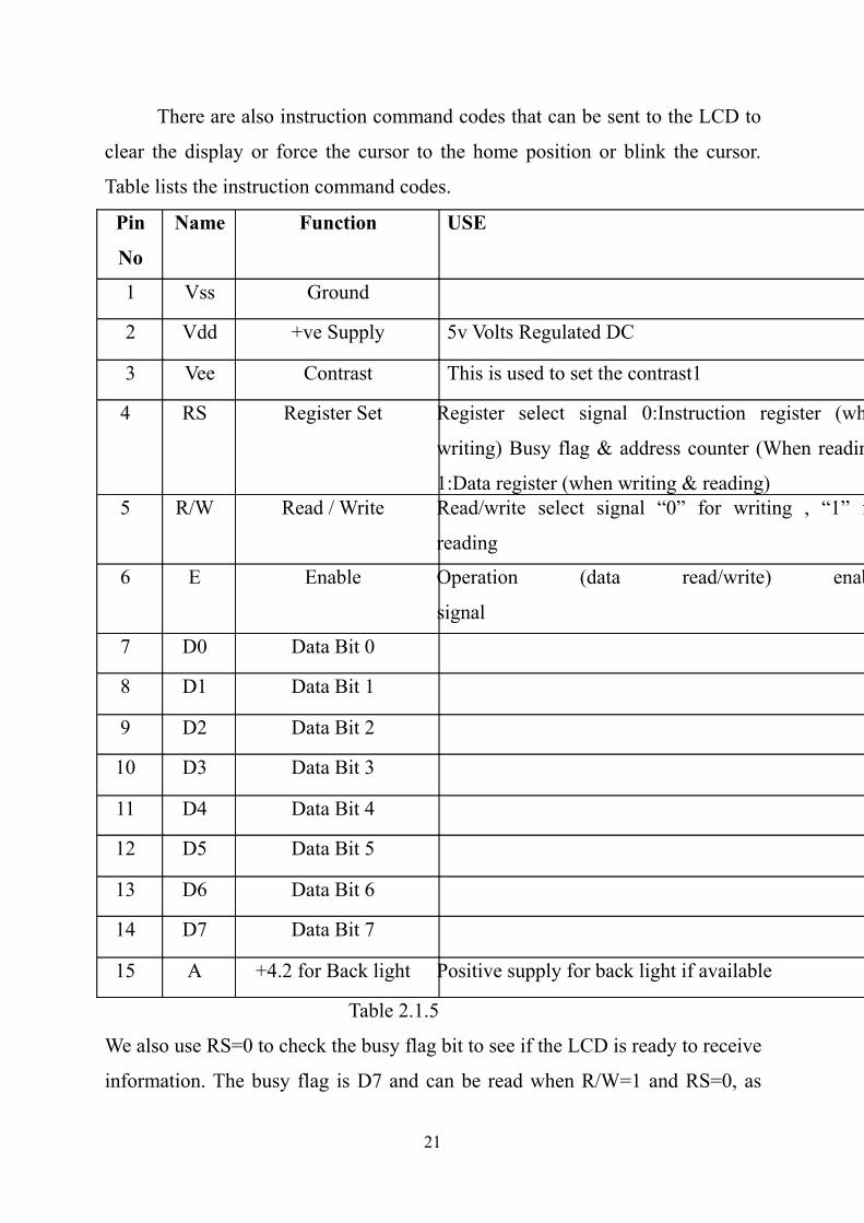
There are also instruction command codes that can be sent to the LCD to
clear the display or force the cursor to the home position or blink the cursor.
Table lists the instruction command codes.
Pin
No
Name Function USE
1 Vss Ground
2 Vdd +ve Supply 5v Volts Regulated DC
3 Vee Contrast This is used to set the contrast1
4 RS Register Set Register select signal 0:Instruction register (when
writing) Busy flag & address counter (When reading)
1:Data register (when writing & reading)5 R/W Read / Write Read/write select signal “0” for writing , “1” for
reading
6 E Enable Operation (data read/write) enable
signal
7 D0 Data Bit 0
8 D1 Data Bit 1
9 D2 Data Bit 2
10 D3 Data Bit 3
11 D4 Data Bit 4
12 D5 Data Bit 5
13 D6 Data Bit 6
14 D7 Data Bit 7
15 A +4.2 for Back light Positive supply for back light if available
Table 2.1.5
We also use RS=0 to check the busy flag bit to see if the LCD is ready to receive
information. The busy flag is D7 and can be read when R/W=1 and RS=0, as
21
follows: if R/W=1, RS=0. When D7=1 (busy flag=1), the LCD is busy taking
care of internal operations and will not accept any new information.
Note: It is recommended to check the busy flag before writing any data .
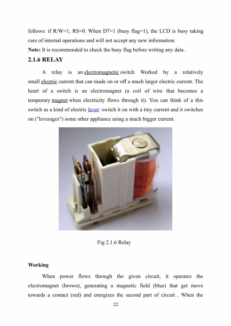
2.1.6 RELAY
A relay is an electromagnetic switch Worked by a relatively
small electric current that can made on or off a much larger electric current. The
heart of a switch is an electromagnet (a coil of wire that becomes a
temporary magnet when electricity flows through it). You can think of a this
switch as a kind of electric lever: switch it on with a tiny current and it switches
on ("leverages") some other appliance using a much bigger current.
Fig 2.1.6 Relay
Working
When power flows through the given circuit, it operates the
electromagnet (brown), generating a magnetic field (blue) that get move
towards a contact (red) and energizes the second part of circuit . When the
22
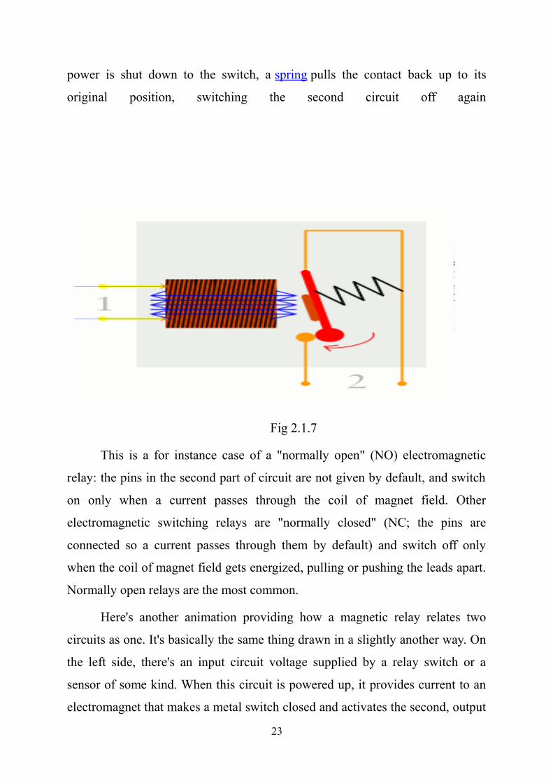
power is shut down to the switch, a spring pulls the contact back up to its
original position, switching the second circuit off again
Fig 2.1.7
This is a for instance case of a "normally open" (NO) electromagnetic
relay: the pins in the second part of circuit are not given by default, and switch
on only when a current passes through the coil of magnet field. Other
electromagnetic switching relays are "normally closed" (NC; the pins are
connected so a current passes through them by default) and switch off only
when the coil of magnet field gets energized, pulling or pushing the leads apart.
Normally open relays are the most common.
Here's another animation providing how a magnetic relay relates two
circuits as one. It's basically the same thing drawn in a slightly another way. On
the left side, there's an input circuit voltage supplied by a relay switch or a
sensor of some kind. When this circuit is powered up, it provides current to an
electromagnet that makes a metal switch closed and activates the second, output
23

circuit (on the right side). The closely required small current in the input circuit
thus energizes the larger current in the output circuit:
Fig 2.1.8
1. The input circuit (black loop) is switched off and no current flows
through it until something (either a sensor or a switch closing) turns it on.
The output circuit (blue loop) is also switched off.
2. When a small current flows in the input circuit, it activates the
electromagnet (shown here as a red coil), which produces a magnetic
field all around it.
3. The energized electromagnet pulls the metal bar in the output circuit
toward it, closing the switch and allowing a much bigger current to flow
through the output circuit.
4.The output circuit operates a high-current appliance such as a lamp or an
electric motor.
2.1.7 GSM MODULE
24

Fig 2.1.9
A GSM modem is a specialized type of modem which accepts a SIM card, and
operates over a subscription to a mobile operator, just like a mobile phone.
From the mobile operator perspective, a GSM modem looks just like a mobile
phone.
When a GSM modem is connected to a computer, this allows the computer to
use the GSM modem to communicate over the mobile network. While these
GSM modems are most frequently used to provide mobile internet connectivity,
many of them can also be used for sending and receiving SMS and MMS
messages.
A GSM modem can be a dedicated modem device with a serial, USB or
Bluetooth connection, or it can be a mobile phone that provides GSM modem
25
capabilities. For the purpose of this document, the term GSM modem is used as
a generic term to refer to any modem that supports one or more of the protocols
in the GSM evolutionary family, including the 2.5G technologies GPRS and
EDGE, as well as the 3G technologies WCDMA, UMTS, HSDPA and HSUPA.
A GSM modem exposes an interface that allows applications such as NowSMS
to send and receive messages over the modem interface. The mobile operator
charges for this message sending and receiving as if it was performed directly
on a mobile phone. To perform these tasks, a GSM modem must support an
“extended AT command set” for sending/receiving SMS messages, as defined in
the ETSI GSM 07.05 and and 3GPP TS 27.005 specifications.
GSM modems can be a quick and efficient way to get started with SMS,
because a special subscription to an SMS service provider is not required. In
most parts of the world, GSM modems are a cost effective solution for receiving
SMS messages, because the sender is paying for the message delivery.
A GSM modem can be a dedicated modem device with a serial, USB or
Bluetooth connection, such as the Falcom Samba 75. (Other manufacturers of
dedicated GSM modem devices include Wavecom, Multitech and iTegno.
We’ve also reviewed a number of modems on our technical support blog.) To
begin, insert a GSM SIM card into the modem and connect it to an available
USB port on your computer.
A GSM modem could also be a standard GSM mobile phone with the
appropriate cable and software driver to connect to a serial port or USB port on
your computer. Any phone that supports the “extended AT command set” for
sending/receiving SMS messages, as defined in ETSI GSM 07.05 and/or 3GPP
TS 27.005, can be supported by the Now SMS & MMS Gateway. Note that not
all mobile phones support this modem interface.
Due to some compatibility issues that can exist with mobile phones, using a
dedicated GSM modem is usually preferable to a GSM mobile phone. This is
more of an issue with MMS messaging, where if you wish to be able to receive
26
inbound MMS messages with the gateway, the modem interface on most GSM
phones will only allow you to send MMS messages. This is because the mobile
phone automatically processes received MMS message notifications without
forwarding them via the modem interface.
It should also be noted that not all phones support the modem interface for
sending and receiving SMS messages. In particular, most smart phones,
including Blackberries, iPhone, and Windows Mobile devices, do not support
this GSM modem interface for sending and receiving SMS messages at all at
all. Additionally, Nokia phones that use the S60 (Series 60) interface, which is
Symbian based, only support sending SMS messages via the modem interface,
and do not support receiving SMS via the modem interface.
2.1.8 RS 232 CABLE
RS-232 is a standard communication protocol for linking computer and its
peripheral devices to allow serial data exchange. In simple terms RS232 defines
the voltage for the path used for data exchange between the devices. It specifies
common voltage and signal level, common pin wire configuration and
minimum, amount of control signals. As mentioned above this standard was
designed with specification for electromechanically teletypewriter and modem
system and did not define elements such as character encoding, framing of
characters, error detection protocols etc that are essential features when data
transfer takes place between a computer and a printer. Without which it could
not be adopted to transfer data between a computer and a printer. To overcome
this problem a single integrated circuit called as UART known as universal
asynchronous receiver/transmitter is used in conjunction with RS232.
27

Fig 2.1.10
RS232 logic and voltage levels
Data circuits Control circuits Voltage
0 (space) Asserted +3 to +15 V
1 (mark) Disserted -15 to -3 V
This is how the entire arrangement works.
It is clear from this figure that UART, line drivers and RS232 are three separate
parts in the system each having its own characteristic features. UART and line
drivers are the parts in RS232 to enhance quality of system during serial data
exchange.
A standard definition was given by EIA to define RS232 as “an interface
between Data terminal equipment and Data communication equipment”. A
typical RS232 system is shown below. DTE-A DTE stands for data terminal
equipment is an end instrument that convert user information into signals or
reconverts the receive signal. It is a functional unit of station that serves as data
28
source or data sink and provides for communication control function according
to the link protocol. A male connector is used in DTE and has pin out
configuration.
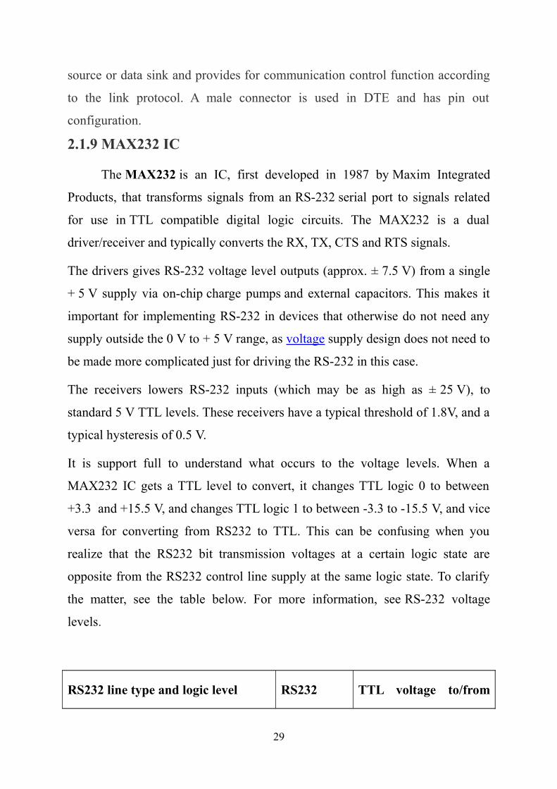
2.1.9 MAX232 IC
The MAX232 is an IC, first developed in 1987 by Maxim Integrated
Products, that transforms signals from an RS-232 serial port to signals related
for use in TTL compatible digital logic circuits. The MAX232 is a dual
driver/receiver and typically converts the RX, TX, CTS and RTS signals.
The drivers gives RS-232 voltage level outputs (approx. ± 7.5 V) from a single
+ 5 V supply via on-chip charge pumps and external capacitors. This makes it
important for implementing RS-232 in devices that otherwise do not need any
supply outside the 0 V to + 5 V range, as voltage supply design does not need to
be made more complicated just for driving the RS-232 in this case.
The receivers lowers RS-232 inputs (which may be as high as ± 25 V), to
standard 5 V TTL levels. These receivers have a typical threshold of 1.8V, and a
typical hysteresis of 0.5 V.
It is support full to understand what occurs to the voltage levels. When a
MAX232 IC gets a TTL level to convert, it changes TTL logic 0 to between
+3.3 and +15.5 V, and changes TTL logic 1 to between -3.3 to -15.5 V, and vice
versa for converting from RS232 to TTL. This can be confusing when you
realize that the RS232 bit transmission voltages at a certain logic state are
opposite from the RS232 control line supply at the same logic state. To clarify
the matter, see the table below. For more information, see RS-232 voltage
levels.
RS232 line type and logic level RS232 TTL voltage to/from
29
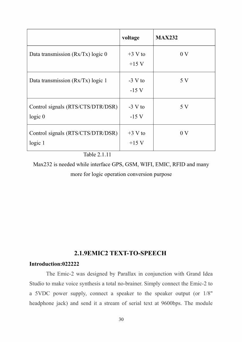
voltage MAX232
Data transmission (Rx/Tx) logic 0 +3 V to
+15 V
0 V
Data transmission (Rx/Tx) logic 1 -3 V to
-15 V
5 V
Control signals (RTS/CTS/DTR/DSR)
logic 0
-3 V to
-15 V
5 V
Control signals (RTS/CTS/DTR/DSR)
logic 1
+3 V to
+15 V
0 V
Table 2.1.11
Max232 is needed while interface GPS, GSM, WIFI, EMIC, RFID and many
more for logic operation conversion purpose
2.1.9EMIC2 TEXT-TO-SPEECH
Introduction:022222
The Emic-2 was designed by Parallax in conjunction with Grand Idea
Studio to make voice synthesis a total no-brainer. Simply connect the Emic-2 to
a 5VDC power supply, connect a speaker to the speaker output (or 1/8"
headphone jack) and send it a stream of serial text at 9600bps. The module
30
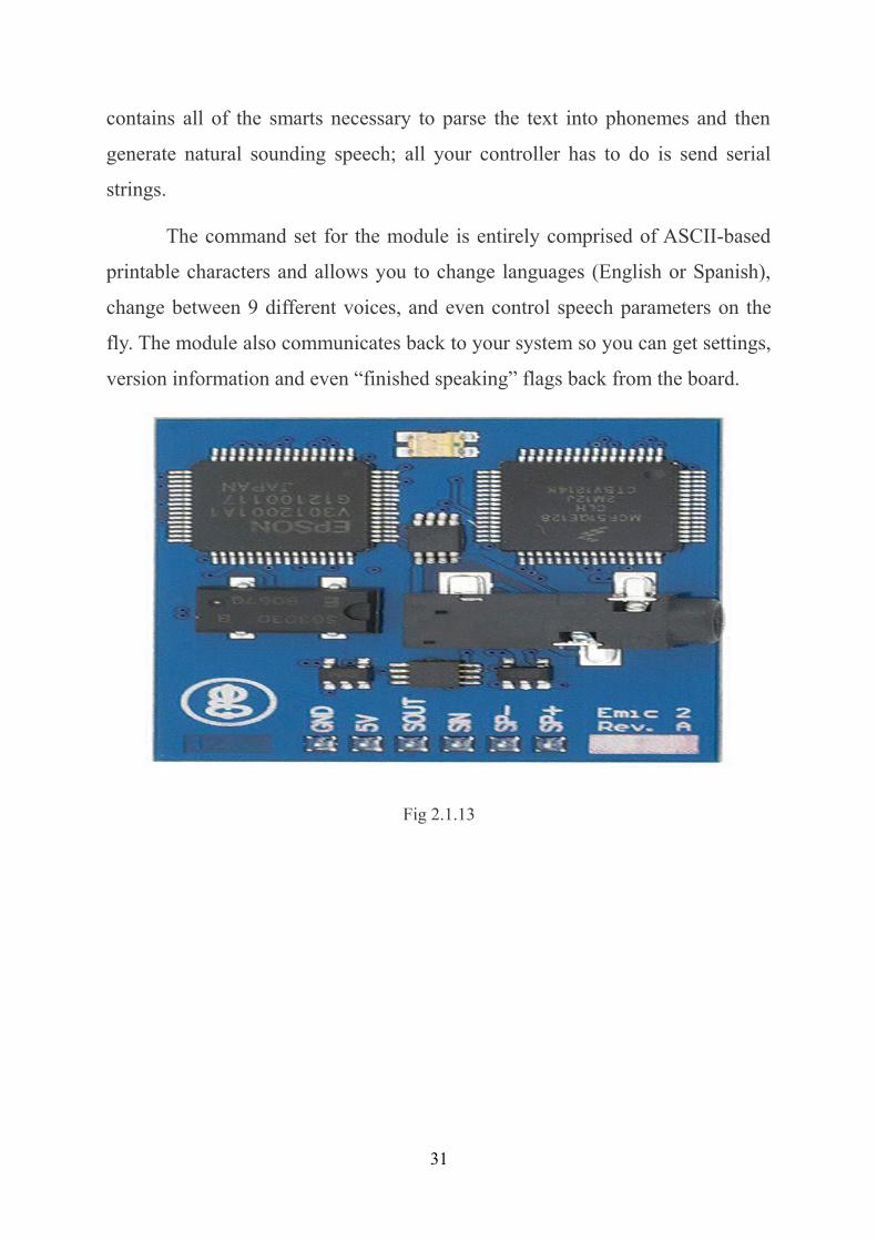
contains all of the smarts necessary to parse the text into phonemes and then
generate natural sounding speech; all your controller has to do is send serial
strings.
The command set for the module is entirely comprised of ASCII-based
printable characters and allows you to change languages (English or Spanish),
change between 9 different voices, and even control speech parameters on the
fly. The module also communicates back to your system so you can get settings,
version information and even “finished speaking” flags back from the board.
Fig 2.1.13
31
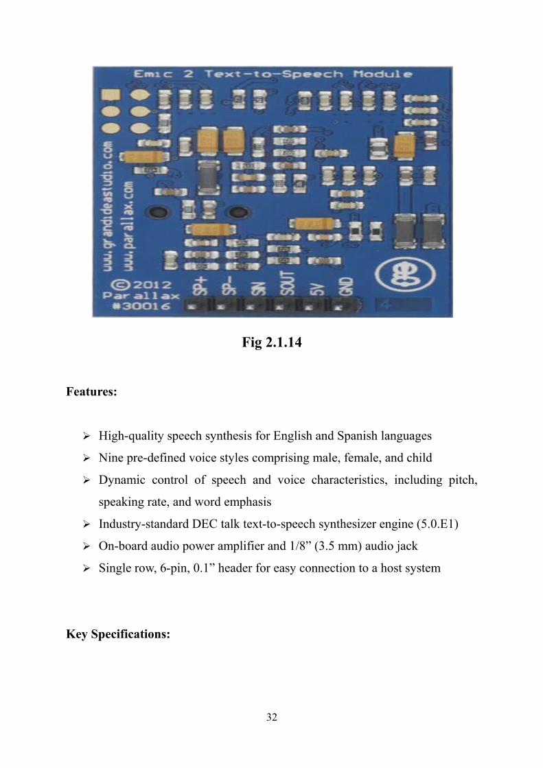
Fig 2.1.14
Features:
High-quality speech synthesis for English and Spanish languages
Nine pre-defined voice styles comprising male, female, and child
Dynamic control of speech and voice characteristics, including pitch,
speaking rate, and word emphasis
Industry-standard DEC talk text-to-speech synthesizer engine (5.0.E1)
On-board audio power amplifier and 1/8” (3.5 mm) audio jack
Single row, 6-pin, 0.1” header for easy connection to a host system
Key Specifications:
32

Power requirements: +5 VDC, 30 mA idle, 46-220 mA active (depending
on speech parameters and output load)
Communication: asynchronous 9600 bps serial
Operating temperature: -20 to +70 °C (-4 to +158 °F)
Dimensions: 1.25” W x 1.5” L x 0.37” H (3.17 W x 3.81 L x 0.94 H cm)
2.2 SOFTWARE DESCRIPTION
2.2.1 KEIL COMPILER
Keil Software publishes one of the most complete development tool
suites for 8051 software, which is used throughout industry. For development of
C code, their Developer's Kit product includes their C51 compiler, as well as an
integrated 8051 simulator for debugging. A demonstration version of this
product is available on their website, but it includes several limitations
The C programming language was designed for computers, though, and
not embedded systems. It does not support direct access to registers, nor does it
allow for the reading and setting of single bits, two very important requirements
for 8051 software. In addition, most software developers are accustomed to
writing programs that will by executed by an operating system, which provides
system calls the program may use to access the hardware. However, much code
for the 8051 is written for direct use on the processor, without an operating
system. To support this, the Keil compiler has added several extensions to the C
language to replace what might have normally been implemented in a system
call, such as the connecting of interrupt handlers.
The purpose of this manual is to further explain the limitations of the Keil
compiler, the modifications it has made to the C language, and how to account
for these in developing software for the 8051 microcontroller.
3.CIRCUT DIAGRAM.
33
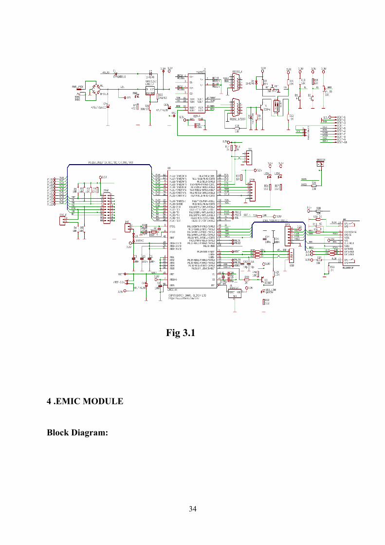
Fig 3.1
4 .EMIC MODULE
Block Diagram:
34

Fig 4.1
Circuit Diagram:
Fig 4.2
For audio output, a connection needs to be made to either SP+/SP- or the 1/8"
audio jack. Audio quality may be affected if both outputs are used at the same
time.
5. PROGRAM LOADED IN ARM7.
#include <lpc214x.h>#include <stdio.h>#include "UART.h"
#define ESC 0x1B#define DONE 0x80000000#define START 0x01000000#define PRESET 0x00230600
35
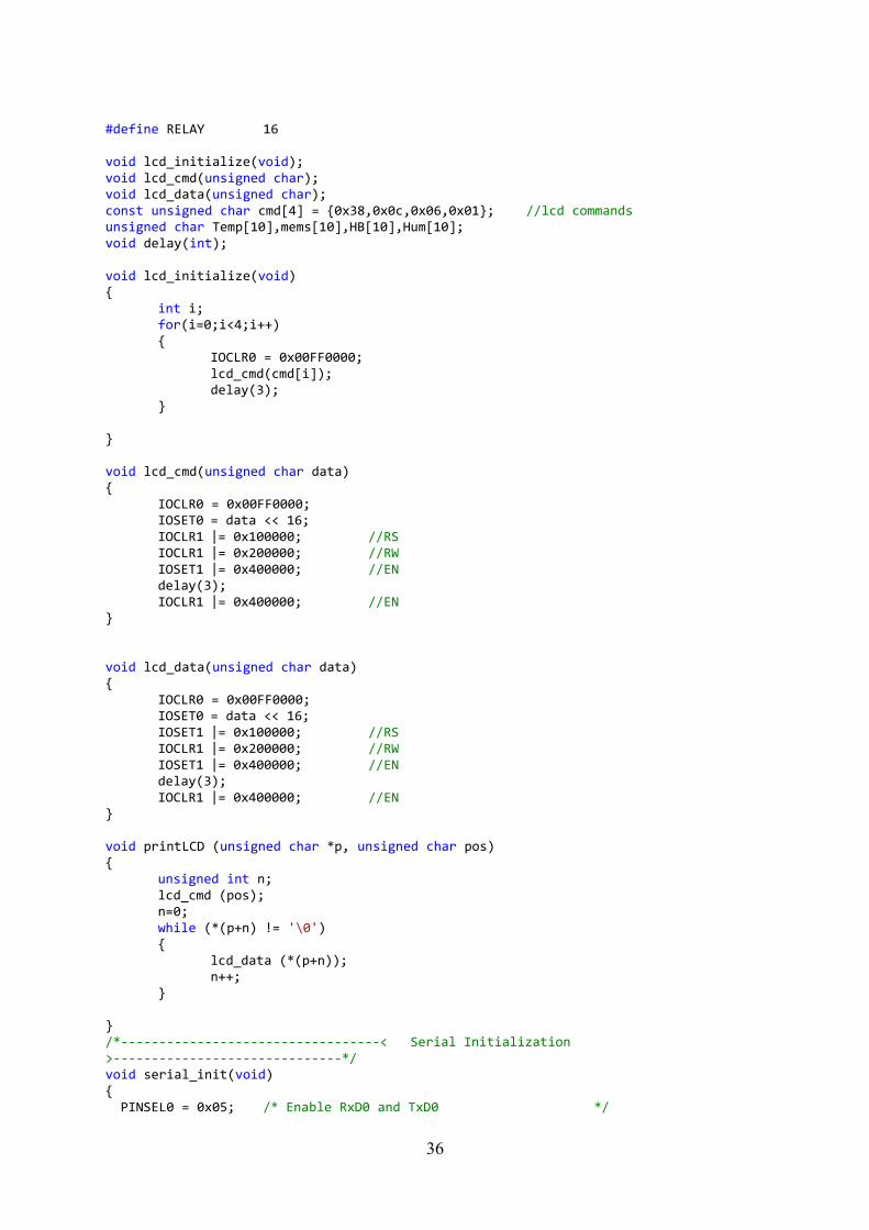
#define RELAY 16
void lcd_initialize(void);void lcd_cmd(unsigned char);void lcd_data(unsigned char);const unsigned char cmd[4] = {0x38,0x0c,0x06,0x01}; //lcd commandsunsigned char Temp[10],mems[10],HB[10],Hum[10];void delay(int);
void lcd_initialize(void){
int i;for(i=0;i<4;i++){
IOCLR0 = 0x00FF0000;lcd_cmd(cmd[i]);delay(3);
}
}
void lcd_cmd(unsigned char data){
IOCLR0 = 0x00FF0000;IOSET0 = data << 16;IOCLR1 |= 0x100000; //RSIOCLR1 |= 0x200000; //RWIOSET1 |= 0x400000; //ENdelay(3);IOCLR1 |= 0x400000; //EN
}
void lcd_data(unsigned char data){
IOCLR0 = 0x00FF0000;IOSET0 = data << 16;IOSET1 |= 0x100000; //RSIOCLR1 |= 0x200000; //RWIOSET1 |= 0x400000; //ENdelay(3);IOCLR1 |= 0x400000; //EN
}
void printLCD (unsigned char *p, unsigned char pos){
unsigned int n;lcd_cmd (pos);n=0;while (*(p+n) != '\0'){
lcd_data (*(p+n));n++;
}
}/*----------------------------------< Serial Initialization >------------------------------*/void serial_init(void){ PINSEL0 = 0x05; /* Enable RxD0 and TxD0 */
36

U0LCR = 0x83; /* 8 bits, no Parity, 1 Stop bit */ U0DLL = 195; /* 9600 Baud Rate @ 12MHz VPB Clock */ U0LCR = 0x03; /* DLAB = 0 */ U0IER = 0x03; /*Enable Interrupt Register */}
//------------------------//Delay Routine start here//------------------------void delay(int n){
int i,j;for(i=0;i<n;i++){
for(j=0;j<0x5000;j++){;}
}}
int main(void){
unsigned long val[4],T;//,G;unsigned int ADC_CH,i=0;
PINSEL0 = 0x00000005; //Enable RXD0 and TXD0PINSEL1 |= 0x01 << 24; //Enable ADC0.1PINSEL1 |= 0x01 << 26; //Enable ADC0.2PINSEL1 |= 0x01 << 28; //Enable ADC0.3PINSEL1 |= 0x01 << 18; //Enable ADC0.4VPBDIV = 0x02; //Set the cclk to 30 MhzAD0CR = 0x00250602; //ADC configuration bits CLK = 9clks/8Bit |
BURST=1 | CLKDIV = 0x06AD0CR |= 0x01000000; //start ADC now
//serial initializationUART1_Init(9600);UART0_Init(9600);U0IER = 1;VICIntSelect = 0<<6; //UART0 ('0' -
irq '1'-fiq)VICVectCntl0 = 0x020 | 6; //VIC slot enabledVICIntEnable = 0x00000040; //Enable UART0 Interrupt
ADC_CH = 1;
IODIR1 |= 1 << RELAY; //Configure P0.16 Output
IOSET1 |= 1 << RELAY;
IODIR0 |= 0xff << 16;IODIR1 |= 0xf << 20;
lcd_initialize();printLCD(" ENERGY ",0x80);printLCD(" MANAGEMENT ",0xC0);delay(25);
lcd_cmd(0x01);
37
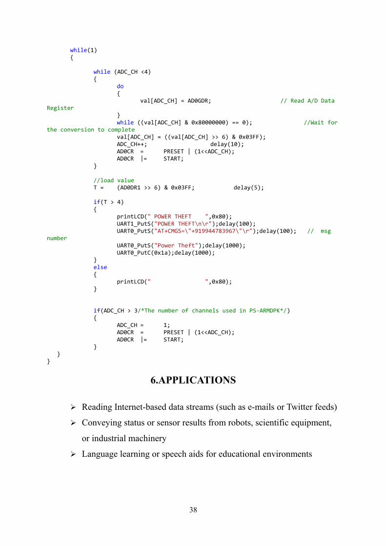
while(1){
while (ADC_CH <4){
do{
val[ADC_CH] = AD0GDR; // Read A/D Data Register
} while ((val[ADC_CH] & 0x80000000) == 0); //Wait for
the conversion to completeval[ADC_CH] = ((val[ADC_CH] >> 6) & 0x03FF);ADC_CH++; delay(10);AD0CR = PRESET | (1<<ADC_CH);AD0CR |= START;
}
//load valueT = (AD0DR1 >> 6) & 0x03FF; delay(5);
if(T > 4){
printLCD(" POWER THEFT ",0x80);UART1_PutS("POWER THEFT\n\r");delay(100);UART0_PutS("AT+CMGS=\"+919944783967\"\r");delay(100); // msg
numberUART0_PutS("Power Theft");delay(1000);UART0_PutC(0x1a);delay(1000);
}else{
printLCD(" ",0x80);}
if(ADC_CH > 3/*The number of channels used in PS-ARMDPK*/){
ADC_CH = 1;AD0CR = PRESET | (1<<ADC_CH);AD0CR |= START;
} } }
6.APPLICATIONS
Reading Internet-based data streams (such as e-mails or Twitter feeds)
Conveying status or sensor results from robots, scientific equipment,
or industrial machinery
Language learning or speech aids for educational environments
38

7.CONCLUSION
Integrating features of all the hardware components used have been
eveloped In it. Presence of every module has been reasoned out and placed
carefully, thus contributing to the best working of the unit. Secondly, using
highly advanced IC’s with the help of growing technology, the project has been
successfully implemented. Thus the paper has been successfully designed and
tested.
39
8.REFERENCES
[1] Yujun Bao and Xiaoyan Jiang, “Design of electric Energy Meter for
long-distance data information transfers which based upon GPRS”,
ISA2009. International Workshop on Intelligent Systems and
Applications,2009
[2] Ashna.K and Sudhish N George, "GSM based automatic energy meter
reading system" IEEE 2013.
[3] B.O.Omijeh and 2G.I.Ighalo” Modeling of GSM-Based Energy
40
Recharge Scheme for Prepaid Meter”- IOSR Journal of Electrical and
Electronics Engineering (IOSR-JEE), 2013
[4] Sudarshan K. Valluru ” Design and Assemble of Low Cost Prepaid
Smart Card Energy Meter – A Novel Design”- International Journal on
Electrical Engineering and Informatics,March 2014
[5] R. Dhananjayan and E. Shanthi”Smart Energy Meter with Instant Billing
and Payment”-International Journal of Innovative Research in Computer
and Communication Engineering March 2014
[6] Subhasis Kar,Sayantan Dutta,Anusree Sarkar and Sougata Das
“Rechargeable Prepaid Energy Meter Based On SMS Technology”International
Journal of Engineering and Innovative Technology
(IJEIT)April 2014.
[7] Sai Kiran Ellenki,Srikanth Reddy G and Srikanth Chan “Advanced
Smart Energy Metering System for Developing Countries”International
Journal Of Scientific Research And Education,2014
41