ele432 - hacettepe universityalkar/ele432/ele432_2.pdf · ele432 advanced digital ... •static...
TRANSCRIPT

ELE432ADVANCED DIGITAL DESIGN
HACETTEPE UNIVERSITYProgramming an FPGA / Design Flow Perspective

Organization of the Week
• Programming an FPGA• Design Flow in FPGA• Static Timing Analysis• VHDL for combinational design

Configuring an FPGA
• Configuration file (bit file)• Configuration data• Configuration commands• Configuration bitstream.

Configuring an FPGA• Any facets of the device that may be
programmed are done so by means of special configuration cells.
• The majority of FPGAs are based on the use of SRAM cells, but some employ FLASH (or E2) cells, while others use antifuses.
Visualizing the SRAM cells as a long shift register.
Each FPGA family typically provides some mechanism such as an initialization pin that, when placed in its active state, causes all of these registers to be returned to their initialization values

Configuring an FPGA

Configuring an FPGA

Verification Design FlowSimple Schematic
Its Netlist representation
Stimulus (Test vectors)

Verification Design Flows

FPGA Place and Route Design FLow
ASIC Place and Route Flow

Advanced FPGA Tool Flow• Equivalency checking
• Synopsys Formality• Floorplanning and layout
• Synopsys Amplify (physical synthesis)• Xilinx Floorplanner or PlanAhead™ software
• Static timing analysis • Synopsys PrimeTime
• Calculating power use• Xilinx XPower
• Edit routing and placement• Xilinx FPGA Editor

Design Flow ComparisonASIC FPGA
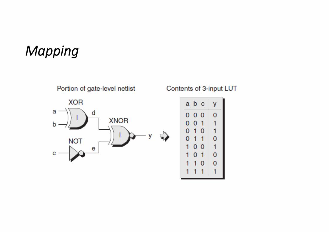
Mapping

Packing• LUTs and registers are packed into the CLBs• packing is a nontrivial problem because there are myriad potential combinations and permutations• Assume a simple design comprising only a couple of handfuls of logic gates that end up being mapped
onto four 3-input LUTs A, B, C, and D.
• Now assume that we’re dealing with an FPGA whose CLBs can each contain two 3-input LUTs. In this case we’ll need two CLBs (called 1 and 2) to contain our four LUTs.
• As a first pass, there are 4! (factorial four = 4 3 2 1 = 24) different ways in which our LUTs can be packed into the two CLBs. Or even less (12) when “mirror images” are eliminated.

Place-and-route• Assume that our two CLBs need to be connected together, but that—purely for the
purposes of this portion of our discussions—they can only be placed horizontally or vertically adjacent to each other, in which case there are four possibilities
• The placement problem is much more complex in the real world with thousands of CLB’s in need of being connected to each other in plenty of different combinations.

Timing analysis and post-place-and-routesimulation• A static timing analysis (STA) utility will be run to calculate all of the
input-to-output and internal path delays and also to check for any timing violations (setup, hold, etc.) associated with any of the internal registers.
• Static timing analysis is a method of validating the timing performance of a design by checking all possible paths for timing violations under worst-case conditions. It considers the worst possible delay through each logic element, but not the logical operation of the circuit.
Timing analysis and post-place-and-routesimulation• The design engineers wish to re simulate their design with accurate
(post-place-and-route) timing information. • In this case, they have to use the FPGA tool suite to generate a new
gate-level netlist along with associated timing information in the form of an industry-standard file format called standard delay format (SDF).

Static Timing Analysis
• In comparison to circuit simulation, static timing analysis is• Faster - It is faster because it does not need to simulate multiple test vectors.• More Thorough - It is more thorough because it checks the worst-case timing
for all possible logic conditions, not just those sensitized by a particular set of test vectors.
• Once again Note this thing : Static timing analysis checks the design only for proper timing, not for correct logical functionality.
• Static timing analysis seeks to answer the question, “Will the correct data be present at the data input of each synchronous device when the clock edge arrives, under all possible conditions?”

Static Timing Analysis
• In static timing analysis, the word static alludes to the fact that this timing analysis is carried out in an input-independent manner. It locates the worst-case delay of the circuit over all possible input combinations. There are huge numbers of logic paths inside a chip of complex design. The advantage of STA is that it performs timing analysis on all possible paths (whether they are real or potential false paths).
• However, it is worth noting that STA is not suitable for all design styles. It has proven efficient only for fully synchronous designs. Since the majority of chip design is synchronous, it has become a mainstay of chip design over the last few decades.

Static Timing Analysis
1. Design is broken down into sets of timing paths,2. Calculates the signal propagation delay along each path3. Checks for violations of timing constraints inside the design and at
the input/output interface.• The STA tool analyzes ALL paths from each and every startpoint to
each and every endpoint and compares it against the constraint that (should) exist for that path. All paths should be constrained, most paths are constrained by the definition of the period of the clock, and the timing characteristics of the primary inputs and outputs of the circuit.

Static Timing Analysis• Setup and Hold Times• To understand the origin of the Setup and Hold time concepts first understand it with respect to a
System as shown in the fig. An Input DIN and external clock CLK are buffered and passes through combinational logic before they reach a synchronous input and a clock input of a D flipflop (positive edge triggered). Now to capture the data correctly at D flip flop, data should be present at the time of positive edge of clock signal at the C pin ( to know the detail just read basis of D flipflop).
http://www.vlsi-expert.com/2011/04/static-timing-analysis-sta-basic-part3a.html

SetUp and Hold Time of a System• There may be only 2 condition.• Tpd DIN > Tpd Clk For capture the data at the same time when Clock signal (positive clock edge)
reaches at pin C, you have to apply the input Data at pin DIN "Ts(in)=(Tpd DIN) - (Tpd Clk)" time before the positive clock edge at pin CLK.
• In other words, at DIN pin, Data should be stable "Ts(in)" time before the positive clock edge at CLK pin. This Time "Ts(in)" is know as Setup time of the System.
• Tpd DIN < Tpd Clk For capture the data at the same time when clock signal (positive clock edge) reaches at pin C, input Data at pin DIN should not change before "Th(in)= (Tpd Clk) - (Tpd DIN)" time. If it will change, positive clock edge at pin C will capture the next data.
• In other words, at DIN pin, Data should be stable "Th(in)" time after the positive clock edge at CLK pin. This time "Th(in)" is know as Hold Time of the System.
http://www.vlsi-expert.com/2011/04/static-timing-analysis-sta-basic-part3a.html

SetUp and Hold Time of a System• Tpd DIN (max) > Tpd Clk (min)SetUp time == Tpd DIN (max) - Tpd Clk (min)• Tpd DIN (min) < Tpd Clk (max)Hold time == Tpd Clk (max) - Tpd DIN (min)
For example for combinational logic delays areData path (max, min) = (5ns, 4ns)Clock path (max, min) = (4.5ns, 4.1ns)Then Setup time= 5-4.1=0.9nsHold time is = 4.5-4=0.5ns
http://www.vlsi-expert.com/2011/04/static-timing-analysis-sta-basic-part3a.html

SetUp and Hold Time of a System - Definition• Setup Time: Setup time is the minimum amount of time the data signal should be held steady before the
clock event so that the data are reliably sampled by the clock. This applies to synchronous circuits such as the flip-flop. Or In short I can say that the amount of time the Synchronous input (D) must be stable before the active edge of the Clock.
• The Time when input data is available and stable before the clock pulse is applied is called Setup time.• Hold time: Hold time is the minimum amount of time the data signal should be held steady after the clock
event so that the data are reliably sampled. This applies to synchronous circuits such as the flip-flop. Or in short I can say that the amount of time the synchronous input (D) must be stable after the active edge of clock.
• The Time after clock pulse where data input is held stable is called hold time.
http://www.vlsi-expert.com/2011/04/static-timing-analysis-sta-basic-part3a.html

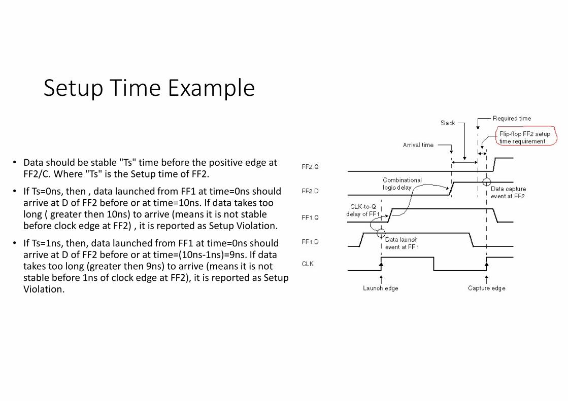
Setup Time Example
Till now we have discussed setup and hold violation with respect to the single flipflop, now lets extend this to 2 flip flop. In the following fig there are 2 flipflops (FF1 and FF2).
Setup Time Example
• Data should be stable "Ts" time before the positive edge at FF2/C. Where "Ts" is the Setup time of FF2.
• If Ts=0ns, then , data launched from FF1 at time=0ns should arrive at D of FF2 before or at time=10ns. If data takes too long ( greater then 10ns) to arrive (means it is not stable before clock edge at FF2) , it is reported as Setup Violation.
• If Ts=1ns, then, data launched from FF1 at time=0ns should arrive at D of FF2 before or at time=(10ns-1ns)=9ns. If data takes too long (greater then 9ns) to arrive (means it is not stable before 1ns of clock edge at FF2), it is reported as Setup Violation.

Hold Time example
In the above fig you can see that there is a delay in the CLK and CLKB because of the delay introduced by the series of buffer in the clock path. Now Flip-flop FF2 has a hold requirement and as per that data should be constant after the capture edge of CLKB at Flip-flop FF2.You can see that desired data which suppose to capture by CLKB at FF2.D should be at Zero (0) logic state and be constant long enough after the CLKB capture edge to meet hold requirement but because of very short logic delay between FF1/Q and FF2/D, the change in the FF1/Q propagates very soon. As a result of that there occurs a Hold violation.This type of violation (Hold Violation) can be fixed by shortening the delay in the clock line or by increasing the delay in the data path.
Setup and Hold violation calculation for the single clock cycle path is very easy to understand. But the complexity increases in case of multi-cycle path ,Gated clock, Flip-flop using different clocks, Latches in place of Flip-Flop. We will discuss all these later sometime.

Flat vs hierarchical schematics
• It was difficult to visualize a high-level, top-down view of the design.
• It was difficult to save and reuse portions of the design in future projects.
• In the case of designs in which some portion of the circuit was repeated multiple times (which is very common), that portion would have to be redrawn or copied onto multiple pages. This became really

Flat vs hierarchical schematics

Different levels of abstraction in HDL based design
The functional level of abstraction:Y = (SELECT & DATA-A) | (!SELECT & DATA-B); -- booleanThis level also encompasses register transfer level (RTL) representations. A design formed from a collection of registers linked by combinational logic. These registers are often controlled by a common clock signal,
when CLOCK risesif CONTROL == “1"then REGA = REGB & REGC;else REGA = REGB | REGD;end if;
end when;
The behavioral (algorithmic) level of abstraction:The highest level of abstraction sported by traditionalHDLs is known as behavioral, which refers to the ability todescribe the behavior of a circuit using abstract constructs likeloops and processes. This also encompasses using algorithmicelements like adders and multipliers in equations;Y = (DATA-A + DATA-B) * DATA-C;

HDL Based Design Flow

Very High Speed Integrated Circuit Hardware Description Language
• VHDL can be used for• documentation • verification • synthesis of large digital designs
Save time & effortfor debugging

VHDL
• VHDL is a standard (VHDL-1076) developed by the IEEE.• First revised in 1987 (Std 1076-1987) then again as VHDL'93.• Initially created for accurate modeling of circuits for simulation• Supports Hierarchy and uses Concurrency.• Supports structural, dataflow and behavioral description styles• Not Technology Specific but supports technology specific functions.• No need to learn a different language for design/simulation/synthesis• Design philosophies: Top down, bottom up and mixed• Test Benches can also be written in VHDL• Capability of defining new data types.

Styles of Modelling
•Behavioral: Algorthnic Representation of Action and Timing
•Functional: Functionality is shown as a series of assignments
•Structural: Hierarchical arrangement of interconnected components.

A VHDL Design may have:
Entity Declaration Architecture Body Configuration Declaration Package Declaration Package Body

Entity Declaration
entity compare isport( A, B: in bit_vector(0 to 7);
EQ: out bit:=‘1’);end compare;
ENTITYcomparator
AB
EQ
An entity declaration specifies the name of the entity being modeled
There are five possible port modes: in, out, inout, buffer and linkage
Initialization is possible at the entity level; Example EQ = ‘1’ and A,B are ‘0’

VHDL Data TypesThe most common VHDL data types are listed below: bit: a 1-bit value representing a wire, possible values '0' or '1' • bit_vector: an array of bits • real: largest range possible, floating point value • integer: normal arithmetic functions can be applied,
typically implemented as a 32-bit data type • enumerated: user defined types • physical: time, voltage, etc. • array: groups of elements of the same type • record: groups of different type objects • access: similar to pointers in C • file: for reading and writing disc files • std_logic: represents a digital logic value,
possible values include '0', '1', 'X' (unknown), 'U' (uninitialised), 'Z’ (high impedance), other types are possible, Better to use package for non standard USE IEEE.Std_logic_1164.all;
• std_logic_vector: an array of std_logic (bus), provided you use the IEEE-Standard Library (non standard)

Data Typessubtype my_integer is integer range 38 to 176;type digit is ('0','1','2','3');type MVL is ('U','0','1','Z');type micro_opn is (load, store, add, sub, mul, div);type micro_opn is (load, store, add, sub, mul, div);type address_word is array (0 to 63) of bit;subtype arith_opn is micro_opn range add to div;subtype middle is digit range '1' to '2';subtype onetotwo is digit;type Module is
recordsize: Integer range 20 to 200;critical_dly : time;no_inputs: my_integer;no_output: my_integer;
end record;Type INTEGER is range –214748647 to 2147483647;
-- possible usages of types in the designsignal control:MVL;variable IC: micro_opn:=store;
--store is the initial value for ICvariable ALU: arith_op;variable latch: MVL;constant add_code: bit_vector := (‘0’,’1’,’1’,’1’,’0’);

Package Declaration• Store declarations like components, types, procedures and functions
package EXAMPLE istype SUMMER is (MAY, JUN, JUL, AUG, SEP);component D_FLIP_FLOP
port(D, CK: in BIT; Q, QBAR:out BIT);end component;constant PIN2PIN_DELAY:TIME := 20 ns;function INT2BIT_VEC(INT_VALUE:INTEGER)
return BIT_VECTOR;end EXAMPLE;
Library DESIGN_LIB;use DESIGN_LIB.EXAMPLE_PACK.all;entity RX is...
Library DESIGN_LIB;use DESIGN_LIB.EXAMPLE_PACK.D_FLIP_FLOP;use DESIGN_LIB:EXAMPLE_PACK.PIN2PIN_DELAY;
At most one package body is used to store the definitions and functions and procedures that were declared in thecorresponding package declaration,

Package Body
package body EXAMPLE_PACK isfunction INT2BIT_VEC (INT_VALUE:INTEGER)
return BIT_VECTOR is begin
-- behavior of function described here…end INT2BIT_VEC;
end EXAMPLE_PACK;
The name of the package body must be the same as the package declaration with which it is associated.

IdentifiersAn identifier in VHDL a sequence of one or more characters.
A legal character is an upper_case letter (A..Z), or a lower case-letter (a..z), or a digit (0..9) or (_).
The first character must be a letter in an identifier.
Identifiers in VHDL are case insensitive.
Two underscore can not appear consecutively.
Ex: DRIVE_BUS, SelectSignal, RAM_Address
SET_CK_HIGH, CONST32_59, r2d2
Comments in a description must be preceded by - - two hyphens.
Ex: -- This is a comment; it ends at the end of the line.
Entity UART is end; -- this comment starts after the entity declaration.

Architecture Body
architecture compare1 of compare isbegin
EQ <= `1' when (A = B) else `0';end compare1;
actual functional description
of thedesign
Unique name Entity name
A ConcurrentConditional Assignment

Structural Description
Entity Declaration
Version1 Version2 Version3
Architecture Bodies
An entity is modeled using one entity declaration &
at least one architecture bodyCONFIGURATION foo of adder is
for testfor u1 : nand2 use entity work.new1(test);end for;
end for;end foo; --- may use at the end of file

Configuration Specification• In a configuration declaration
Architecture structure of full_adder iscomponent or2 port(A,B: in bit; Z: out bit);end component;-- other components hereBegin
P1:or2 port map (c,d,e); -- other port mapsEnd structurelibrary cmos_lib,work;configuration prefered of full_adder is
For structure – configuration specificationfor P1: or2use entity cmos_lib.or2(or2tr); end for;
End for;end prefered;

Behavioral vs. Structural Description• An entity can be described by
• its behavior
• its structure,
• in a mixed fashion
• Example: a 2-input XOR gate
A
B
Y
Y = A.B+A.B
A
B
Y
G1
G2
G4
G3

XOR in VHDL: Behavioral
entity XOR isport ( A,B : in bit; Y : out bit);
end XOR;
architecture behavioral of XOR isbegin
Y <= (A and not B) or (not A and B);end behavioral;

XOR in VHDL: Structure
architecture STRUCTURE of XOR iscomponent NAND
port ( A, B : in bit; Y : out bit);end component;signal C, D, E : bit;
beginG1 : NAND port map (A, B, C);G2 : NAND port map
(A => A, B => C, Y => D);G3 : NAND port map
(C, B => B, Y => E);G4 : NAND port map (D, E, Y);
end STRUCTURE;Component Instantiation
is just anotherConcurrent Statement!

XOR in VHDL: Mixed
architecture MIXED of XOR iscomponent NAND
port ( A, B : in bit; Y : out bit);end component;signal C, D, E : bit;
beginD <= A nand C;E <= C nand B;G1 : NAND port map (A, B, C);G4 : NAND port map (D, E, Y);
end MIXED;

OperatorsPredefined Operators:1- Logical: and, or, nand, nor, xor, not2- Relational Operators =, /= ,< , <= , > , >=3- Arithmetic Operators +, -, & (concatenation), *, /, mod (modulus)rem (remainder), abs(absolute), **,
ex: A rem B = A - (A/B) * BA mod B = A - B * N -- for some integer N
Overloading Operators:package math is
function “+”(l.r: bit_vector)return integer;
end math;package body math is …end math;
use work.math.all;entity adder isport (a,b : in bit_vector(0 to 7);c : in integer;
dout : out integer);end adder;architecture test of adder is
signal internal : integer;begin -- E X A M P LE
internal <= a+b;dout <= c+internal;
end test;

VHDL Objects
• Signals
Variables NOW
Concurrent!!
Constants

Constants
Constant RISE_TIME: TIME:=10ns; -- Time is the type
Constant BUS_WIDTH:INTEGER:=8; -- integer is the type value 8.

Declaration of SignalsArchitecture arch1 of my_design is -- DECLARATIVE PART BELOW
Signal Q: std_logic:=‘X’; -- optional initial value assignmentSignal bus1, bus2: std_logic_vector(7 downto 0); -- END DECLARATIONSBegin
. . .End arch1;
package my_package issignal Q: std_logic; -- Global signal
end my_package;-- this is the other form of declaration use work.my_package.Q; -- Make Q visible to this architecturearchitecture arch1 of my_design is (use “all” for everything)begin
. . .end arch1;