effects of the physical parameter on gate all around fet
TRANSCRIPT

Effects of the physical parameter on gate all around FET
AMIT AGARWAL1, P C PRADHAN1 and BIBHU P SWAIN2,*
1Department of Electronics and Communication Engineering, Sikkim Manipal Institute of Technology, Sikkim
Manipal University, Majhitar, Rangpo 737136, India2Department of Physics, National Institute of Technology, Imphal 795004, India
e-mail: [email protected]; [email protected]; [email protected]
MS received 11 December 2018; revised 4 May 2019; accepted 11 October 2019
Abstract. As the devices are getting compact, the size of transistors reduces day by day; however, with certain
limitations. Due to miniaturization, the characteristics of the transistor change due to quantum mechanical
effects and the present scenario, analytically modeled surface potential-based gate all around (GAA) FET model
by solving 1-D Poisson’s equation, approximation method and using necessary boundary condition. Here, the
change in channel material (Si, InP, GaAs, InAs and Ge), channel radius (varied from 6 nm to 10 nm), oxide
thickness (changed from 2 nm to 5 nm), drain to source voltage (varied from -0.5 V to 0.5 V), Source/Drain
doping (varied from 1017 to 1022/cm3) and temperature (from 0 to 300 K) of the transistor, surface potential
changes from -1.6 V to 1.3 V approx. respectively, considered as the GAA FET parameters. The proposed
novel model exhibits better control over hot carrier effect, Drain Induced Barrier Lowering (DIBL), reduced
threshold voltage and other such short channel effects in the GAA FET. Moreover, the I–V characteristics of the
GAA FET were analyzed. The MATLAB code is used for modeling of the GAA FET nanowire transistor.
Keywords. Gate all around (GAA) MOSFET; nanowire; cylindrical channel; short channel effects (SCEs).
1. Introduction
To govern Moore’s law reality [1], the transistor must be
scaled down from classical dimension to quantum scale by
reducing the channel length, replacing low k dielectric to
high k dielectrics and a new structural approach from pla-
nar MOSFET to 3D FinFET which leads to increase in the
speed and reduces cost. However, with deep scaling,
unwanted effects come into play; these effects are termed
as short channel effects (SCEs) [2]. In SCEs, the channel
length is in the order of depletion layer width of the drain
and source. Due to these SCEs, the performance of the
transistor is affected [3] which leads to various drawbacks
like drain induced barrier lowering (DIBL), velocity satu-
ration, hot carrier effect, threshold voltage roll-off, surface
scattering and rise in leakage current [4]. Due to the DIBL
effect, the gate is ineffective as there is an electrostatic
decoupling between drain and source. With the decrease in
on/off ratio, completely turning OFF transistor is difficult.
This effect is due to the lowering of the threshold voltage.
As the gate length is decreased, the electric field between
source and drain increases and becomes larger. With this
high value of the electric field, the proportionate relation-
ship is violated, which leads to velocity saturation eventu-
ally leading to a decrease in the current drive. With the
reduction of channel length, there is a lowering of threshold
voltage, there is an increase in sub-threshold leakage cur-
rent which increases power dissipation. Due to miniatur-
ization of channel length, the surface to volume ratio
increases, this is a major cause for surface effect and
increases the mean free path of electrons. Hence, with an
increase in surface scattering, the mobility of charge car-
riers degrades. The above key factor reduces the perfor-
mance of the planar structure. Therefore, electrostatic
veracity is improved with the increase in the number of
gates for channel width and height below 10 nm. Some of
the major key steps to reduce SCEs are to (a) implicate
strained channel, and (b) modified the gate structures, i.e.
PD-SOI-FET, and FD-SOI-FET, double gate, Fin-FET,
triple gate, Pi gate, omega gate, square gate (G4) all around
and cylindrical gate all around MOSFET. In double-gate
MOSFET [5], there are two gates (one above the channel
and the other below the channel) which shows better
electrostatic potential control over the channel as compared
to single gate FET. The Fin FET structure resembles a set
of fins [6], which have better electrical control over the
channel to reduce the leakage current and overcome other
SCEs. The effective channel length of the device is deter-
mined by the thickness of the fin [7]. Triple gate FET
having three gates, surrounding the three sides of the
channel [8], shows the high current driving capability and
better gate control over the channel up to 10 nm channel*For correspondence
Sådhanå (2019) 44:248 � Indian Academy of Sciences
https://doi.org/10.1007/s12046-019-1232-8Sadhana(0123456789().,-volV)FT3](0123456789().,-volV)

[9]. In Pi gate MOSFET, the gate is grown into a buried
oxide and enhances electrostatic potential control in the
channel and thus protecting it from the electric-field lines
which are originating from the drain [10]. Omega-FET
exhibits better scaling down characteristics where the gate
is almost wrapped around the channel. Omega-FET is
almost like GAA concerning electrical performance, but it
suffers from severe corner effects [11]. The square gate has
four gates (square shape) all around the channel of FET
[12] and surrounds the entire channel which can reduce
SCEs to some extent, but there exists another problem, i.e.
corner effect. These corner effects can be reduced by using
a cylindrical channel. In cylindrical gate all around MOS-
FET, the channel is entirely wrapped and is cylindrical.
Gate all around (GAA) transistor outperforms all other
multi-gate transistors due to gate wrapped all over the
channel which has better electrostatic control over the
channel and reduces SCEs. This shows that GAA MOSFET
is the future prominent candidate for scaling down of the
MOSFET and governs Moore’s law [13]. In GAA MOS-
FET there are four gates i.e. top gate, bottom gate, and two
side gates. In comparison to the double gate MOSFET,
there are two additional gates so there are two additional
inversion channels created which leads to allowing further
scale down of FET.
In this paper, we have modeled GAA MOSFET using
Poisson’s equation with varying physical parameters such
as channel material ‘et’ (i.e. Si, InP, GaAs, InAs and Ge),
channel radius ‘r’, oxide thickness ‘tox’, gate to source
voltage ‘VGS’, drain to source voltage ‘VDS’, Source/Drain
doping ‘ND’ and temperature ‘T’. With these changes in the
physical parameters, we have found variations in the sur-
face potential of the transistor. Also, we have plotted the I–
V characteristics curve for GAA FET.
2. Analytical modeling of gate all around nanowiretransistor
The front and side views of the cylindrical GAA nanowire
MOSFET structure are shown in figure 1. The structure
modeled is cylindrical in shape with a nanowire channel at
the center. This channel is completely wrapped with an
insulator and finally with the gate.
Analytical modeling of GAA MOSFET is done by
solving cylindrical Poisson’s equation, parabolic approxi-
mation method, and necessary boundary conditions
[14–19].
The 2-D Poisson’s equation for cylindrical GAA MOS-
FET is given by
1
r:o
orr:
o
oru r; zð Þ
� �þ o
oz:
o
ozu
� �¼ q:NA
etð1Þ
where u is the channel potential as a function of radius ‘r’
and channel length ‘z’.
Considering the parabolic approximation, we obtain
u r; zð Þ ¼ g0 zð Þ þ g1 zð Þr þ g2 zð Þr2 ð2Þ
where g0 zð Þ; g1 zð Þ; g2 zð Þ are the coefficients as a function of
‘z’.
Coefficient g0 zð Þ; g1 zð Þ; g2 zð Þ in Eq. 2 can be obtained by
considering the following boundary condition:
i) Electric flux at the interface of SiO2/Si is given by
o
oru r; zð Þ ¼ eox
et:VGS � Vfb � us
toxð3Þ
where Vfb;us are flat band voltage and surface
potential, respectively.
ii) The electric field at the center of the channel is zero.
E r; zð Þj:r¼0 ¼ 0 ð4Þ
iii) The potential at the interfaces of the drain channel
and source channel is
u r; 0ð Þ ¼ Vbuilt�in ð5Þ
and
u r; Lð Þ ¼ Vbuilt�in þ VDS ð6Þ
where Vbuilt�in is built-in voltage, VDS is a drain to source
voltage.
By applying the above boundary condition, the surface
potential for n channel is obtained as
us ¼ Cekz þ De�kz þ / ð7Þ
where / is given by
/ ¼ VGS � Vfb �q:NA
et:k2ð8Þ
where k is the natural length and is given by
k2 ¼ 2:eoxet:R2:ln 1 þ tox
R
� � ð9Þ
The coefficient C and D is given by
C ¼Vbi þ /ð Þ: 1 � e�kL
� �þ VDS
2 sin kLð Þ ð10Þ
and
D ¼Vbi þ /ð Þ: ekL � 1
� �� VDS
2 sin kLð Þ ð11Þ
The complete 2-D potential can be written as
u r; zð Þ ¼ us þCox
2:et:R: VGS � Vfb � us
� �: r2 � R2� �
ð12Þ
248 Page 2 of 7 Sådhanå (2019) 44:248

3. Results and discussion
We have considered these parameters, i.e. radius dimension
R = 5 nm, oxide thickness tox = 2 nm, channel length
L = 15 nm, VDS = 20.1 V and VGS = 1 V for simulation
of the GAA nanowire MOSFET.
Figure 2 shows the plot between surface potential and
channel material of GAA MOSFET with different channel
lengths. The voltage difference between the body and the
gate of the device generates an electric field that controls
the conductivity between source and drain. As the valence
‘EV’ and conduction ‘EC’ band are modified in the channel
material. Due to this, there is a change in energy gap ‘Egap’
of the material which leads to change in built-in potential
‘Vbi’ and further change in surface potential ‘us’ of the
device (given by us ¼ EFið Þsurface� EFið ÞBulk and Vfb ¼ ;�vm � Ec þ EF). From Eq. 7 and Eq. 8, we find the pro-
portional relationship between surface potential, natural
length and channel permittivity. From figure 2, we analyze
that, when we use Ge as channel material with permittivity
16 e0(F/m), the surface potential is approx. 0.89 V and with
Si with permittivity 11.9 e0 (F/m), the surface potential is
0.86 (for a channel length of 10 nm) which shows a devi-
ation of 0.03 V. So, with the increase of channel material
permittivity, surface potential increases.
Figure 3 shows the plot between surface potential and
donor concentration ‘Nd’ of GAA MOSFET with different
channel length ‘L’. With the change in doping, built-in
potential (Vbi) changes (as given by relationship
Vbi ¼ kTqln NAND
n2i
� �) and as per Eq. 7 to Eq. 11, there is a
change in surface potential ‘us’. From this figure, we
investigate that with the increase of donor concentration
‘Nd’ the surface potential increases. When donor concen-
tration is of 1017 cm-3 at 10 nm channel length, the surface
potential is approx. 0.90 V and with donor concentration of
1022 cm-3, the surface potential is approx. 0.93 V. The
maximum of sub-threshold swing, minimum threshold
voltage, and maximum leakage are observed at the same
doping level. There is a deviation of 0.03 V in the surface
potential to change of donor concentration. Also, with the
change in channel length from 10 nm to 15 nm, the surface
potential changes from 0.90 V to 1.1 V.
Figure 4 shows the plot between surface potential and
channel radius of GAA MOSFET with different channel
Figure 1. Schematic of gate all around nanowire transistor.
Figure 2. Surface potential vs channel material varying with
channel length. Device parameter: radius R = 5 nm, oxide thick-
ness tox = 2 nm, VDS = 20.1 V and VGS = 1 V, T = 300 K,
channel length L varied from 10 to 15 nm and channel material Si,
InP, GaAs, InAs, Ge was used. With increase of channel material
permittivity, surface potential of the channel increases.
Sådhanå (2019) 44:248 Page 3 of 7 248
lengths. The movement of the carriers from source to drain
takes place through the channel, with the change in the
physical size of the channel, i.e. length ‘L’ and radius ‘R’ in
the deep sub-micron region, the characteristics of the
device changes. Also, with the change in channel radius
‘R’, natural length changes as per the relationship
k2 ¼ 2:eoxet :R2:ln 1þtox
Rð Þ. So, with the increase in the dimension of
the channel, the surface potential should also increase.
From figure 4, we investigated that surface potential
increases ‘us’ with the increase of channel radius ‘R’ from
5 to 10 nm. The surface potential with radius 5 nm is
approx. 0.87 V at 10 nm channel length and when the
channel radius is 10 nm, the surface potential is approx.
0.91 V, so there is a deviation of approx. 0.04 V in surface
potential. When the thin film thickness is reduced, the
controllability of the gate over the channel becomes
stronger in comparison with the influence exerted by the
source/drain. Also, with the change in channel length from
10 to 15 nm, the surface potential changes from 0.87 V to
0.99 V, with a deviation of 0.12 V.
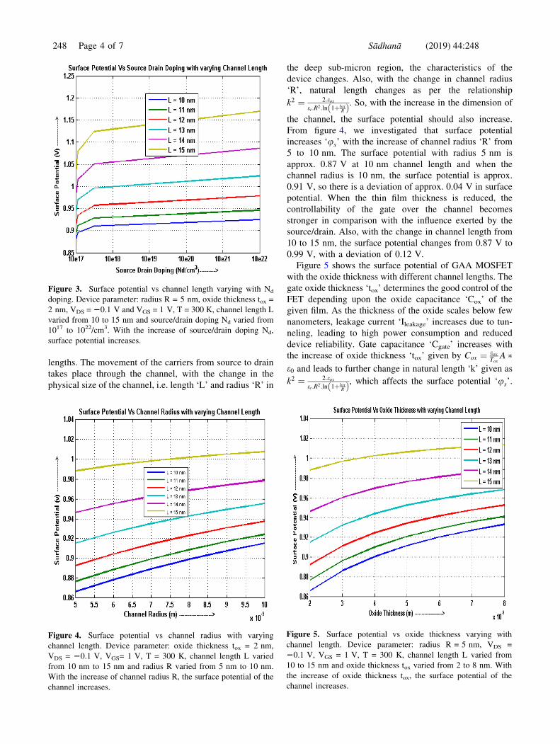
Figure 5 shows the surface potential of GAA MOSFET
with the oxide thickness with different channel lengths. The
gate oxide thickness ‘tox’ determines the good control of the
FET depending upon the oxide capacitance ‘Cox’ of the
given film. As the thickness of the oxide scales below few
nanometers, leakage current ‘Ileakage’ increases due to tun-
neling, leading to high power consumption and reduced
device reliability. Gate capacitance ‘Cgate’ increases with
the increase of oxide thickness ‘tox’ given by Cox ¼ eoxTox
A �e0 and leads to further change in natural length ‘k’ given as
k2 ¼ 2:eoxet :R2:ln 1þtox
Rð Þ, which affects the surface potential ‘us’.
Figure 3. Surface potential vs channel length varying with Nd
doping. Device parameter: radius R = 5 nm, oxide thickness tox =
2 nm, VDS = 20.1 V and VGS = 1 V, T = 300 K, channel length L
varied from 10 to 15 nm and source/drain doping Nd varied from
1017 to 1022/cm3. With the increase of source/drain doping Nd,
surface potential increases.
Figure 4. Surface potential vs channel radius with varying
channel length. Device parameter: oxide thickness tox = 2 nm,
VDS = 20.1 V, VGS= 1 V, T = 300 K, channel length L varied
from 10 nm to 15 nm and radius R varied from 5 nm to 10 nm.
With the increase of channel radius R, the surface potential of the
channel increases.
Figure 5. Surface potential vs oxide thickness varying with
channel length. Device parameter: radius R = 5 nm, VDS =
20.1 V, VGS = 1 V, T = 300 K, channel length L varied from
10 to 15 nm and oxide thickness tox varied from 2 to 8 nm. With
the increase of oxide thickness tox, the surface potential of the
channel increases.
248 Page 4 of 7 Sådhanå (2019) 44:248
From figure 5 we observe that, when the oxide thickness is
2 nm with channel lengths ‘L’ of 10 nm, the surface
potential is approx. 0.87 V however, when the oxide
thickness is 8 nm and the surface potential is approx.
0.93 V, which shows a deviation of 0.06 V in surface
potential. With the increase of oxide thickness, the surface
potential also increases. Thicker oxide can be used to
improve gate dielectric reliability and reduce leakage cur-
rent flowing through the structure. Also, when the channel
length is changed from 10 to 15 nm, the surface potential
changes from 0.87 V to 0.99 V.
Figure 6 shows the surface potential varies with gate to
source voltage ‘VDS’ of GAA MOSFET with different
channel length ‘L’ varying from 10 to 15 nm. The gate to
source voltage ‘VDS’ is an important factor for turning ON/
OFF transistor. The surface potential ‘us’ increases rapidly
from 21.6 to 0.1 V as the gate to source voltage ‘VGS’
increases from 20.5 to 0.5 V.
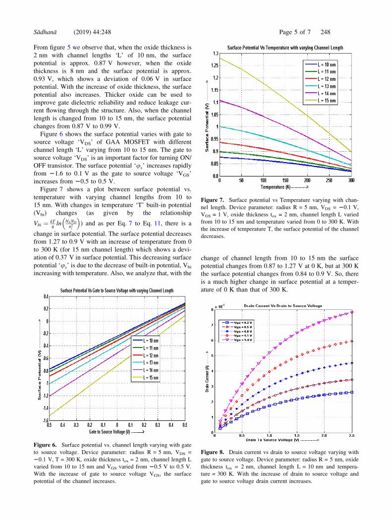
Figure 7 shows a plot between surface potential vs.
temperature with varying channel lengths from 10 to
15 nm. With changes in temperature ‘T’ built-in potential
(Vbi) changes (as given by the relationship
Vbi ¼ kTqln NAND
n2i
� �) and as per Eq. 7 to Eq. 11, there is a
change in surface potential. The surface potential decreases
from 1.27 to 0.9 V with an increase of temperature from 0
to 300 K (for 15 nm channel length) which shows a devi-
ation of 0.37 V in surface potential. This decreasing surface
potential ‘us’ is due to the decrease of built-in potential, Vbi
increasing with temperature. Also, we analyze that, with the
change of channel length from 10 to 15 nm the surface
potential changes from 0.87 to 1.27 V at 0 K, but at 300 K
the surface potential changes from 0.84 to 0.9 V. So, there
is a much higher change in surface potential at a temper-
ature of 0 K than that of 300 K.
Figure 6. Surface potential vs. channel length varying with gate
to source voltage. Device parameter: radius R = 5 nm, VDS =
20.1 V, T = 300 K, oxide thickness tox = 2 nm, channel length L
varied from 10 to 15 nm and VGS varied from 20.5 V to 0.5 V.
With the increase of gate to source voltage VGS, the surface
potential of the channel increases.
Figure 7. Surface potential vs Temperature varying with chan-
nel length. Device parameter: radius R = 5 nm, VDS = 20.1 V,
VGS = 1 V, oxide thickness tox = 2 nm, channel length L varied
from 10 to 15 nm and temperature varied from 0 to 300 K. With
the increase of temperature T, the surface potential of the channel
decreases.
Figure 8. Drain current vs drain to source voltage varying with
gate to source voltage. Device parameter: radius R = 5 nm, oxide
thickness tox = 2 nm, channel length L = 10 nm and tempera-
ture = 300 K. With the increase of drain to source voltage and
gate to source voltage drain current increases.
Sådhanå (2019) 44:248 Page 5 of 7 248

Figures 8 and 9 show output (ID–VDS) and transfer
characteristics (ID–VGS) for a cylindrical gate all around
FET. These figures show that with the increase of drain to
source voltage and gate to source voltage drain current
increases. When the gate voltage is 0.2 V and 1.4 V, drain
current changes from 2.5 to 8 lA at a drain voltage of
2.5 V. When drain voltage is 0.1 V to 1.6 V, the drain
current changes from 1 to 8.5 lA. From these I–V curves,
we find that GAA FET shows good control over the
channel.
4. Conclusion
Modeling of n-channel GAA MOSFET has been done using
Poisson’s equation and simulated using MATLAB code.
The changes in the channel radius from 5 nm to 10 nm and
10 nm channel length, surface potential changes from
0.87 V to 0.91 V and 0.86 to 0.89 V respectively, for the
channel material permittivity 11.9 e0 (F/m) (Si) to 16 e0 (F/
m) (Ge). The surface potential varied from 0.87 V to
0.83 V, with a change of gate to source voltage from 20.5
to 0.5 V and the surface potential also increases 21.6 to
0.1 V at the temperature changes from 0 K to 300 K. With
the analyses of change in surface potential with the varia-
tion in different physical parameters of the device, best
device configuration can be accomplished, and SCEs can be
reduced. Also, we have shown the output (ID–VDS) and
transfer (ID–VGS) characteristics of GAA FET from which
we find that with the increase of drain to source voltage and
gate to source voltage, drain current increases.
References
[1] Moore G E 1998 Cramming more components onto the
integrated circuits. (Reprinted from Electronics,
pp. 114–117, April 19, 1965) Proceedings of the IEEE 86:
82–85
[2] Young K K 1989 Short-channel effects in fully depleted SOI
MOSFETs. IEEE Trans. Electron Devices 36: 399–402
[3] Oh S H, Monroe D and Hergenrother J M 2000 Analytic
description of short-channel effects in fully-depleted double-
gate and cylindrical, surrounding-gate MOSFETs. IEEE
Electron Device Lett. 21: 445–447
[4] Park J T and Colinge J P 2002 Multiple-gate SOI MOSFETs:
device design guidelines. IEEE Trans. Electron Devices 49:
2222–2229
[5] Dhiman G and Ghosh P K 2017 Analytical modeling of
threshold voltage for double-gate MOSFET. International
Conference on Energy, Communication, Data Analytics and
Soft Computing (ICECDS), pp. 1584–1588
[6] Wang H, Liu Y, Han G, Shao Y, Zhang C, Feng Q, Zhang J
and Hao Y 2017 Performance enhancement in uniaxially
strained Germanium–Tin FinTFET: Fin direction depen-
dence. IEEE Trans. Electron Devices 64: 2804–2811
[7] Jagtap S M and Gond V J 2017 Study the performance
parameters of novel scale FINFET Device in nm Region.
International conference of Electronics, Communication and
Aerospace Technology, pp. 424–430
[8] Das S, Choudhury A, Ghosh S, Sarkar S, Chanda M and De
S 2017 Parameter modeling of linearly doped double-gate
MOSFET with high-k dielectrics. Devices for Integrated
Circuit, pp. 136–140
[9] Colinge J P 2007 FinFETs and other multi-gate transistors.
Springer.
[10] Hsieh D, Lin J, Kuo P and Chao T 2017 Comprehensive
analysis on electrical characteristics of Pi-Gate poly-Si
Junctionless FETs. IEEE Trans. Electron Devices 64:
2992–2998
[11] Gupta N, Vohra A and Chaujar R 2016 Linearity perfor-
mance of Gate Metal Engineered (GME) Omega gate-silicon
nanowire MOSFET: a TCAD study. IEEE International
Conference on Electron Devices and Solid-State Circuits,
pp. 208–211
[12] Samoju V R, Mahapatra K and Tiwari P K 2017 Analytical
modeling of subthreshold characteristics by considering
quantum confinement effects in ultrathin dual-metal quadru-
ple gate (DMQG) MOSFETs. Superlattices Microstruct.
111: 704–713
[13] Rahman F, Shakya B, Xu X, Forte D and Tehranipoor M
2017 Security beyond CMOS: fundamentals, applications,
and roadmap. IEEE Trans. Very Large Scale Integr. (VLSI)
Syst. 25: 3420–3433
[14] Djeffal F, Ghoggali Z, Dibi Z and Lakhdar N 2009
Analytical analysis of nanoscale multiple-gate MOSFETs
including effects of hot-carrier induced interface charges.
Microelectron. Reliab. 49: 377–381
Figure 9. Drain current vs gate to source voltage varying with
drain to source voltage. Device parameter: radius R = 5 nm, oxide
thickness tox = 2 nm, channel length L = 10 nm and tempera-
ture = 300 K. With the increase of drain to source voltage and
gate to source voltage drain current increases.
248 Page 6 of 7 Sådhanå (2019) 44:248

[15] Gautam R, Saxena M and Gupta R S 2013 Gate-all-around
nanowire MOSFET with catalytic metal gate for gas sensing
applications. IEEE Trans. Nanotechnol. 12(6): 932–939
[16] Pandian M K and Balamurugan N B 2014 Analytical
threshold voltage modeling of surrounding gate silicon
nanowire transistors with different geometries. J. Electr.
Eng. Technol. 9: 2079–2088
[17] Kumar M, Haldar S, Gupta M and Gupta R S 2016 Physics-
based analytical model for surface potential and subthreshold
current of cylindrical Schottky Barrier gate all around
MOSFET with high-k gate stack. Superlattices Microstruct.
90: 215–226
[18] Ray B and Mahapatra S 2008 Modeling and analysis of body
potential of cylindrical gate-all-around nanowire transistor.
IEEE Trans. Electron Devices 55: 2409–2416
[19] Chen X and Tan C M 2014 Modeling and analysis of gate-
all-around silicon nanowire FET. Microelectr. Reliab. 54:
1103–1108
Sådhanå (2019) 44:248 Page 7 of 7 248