ecng3016_lab2
DESCRIPTION
Digital ElectronicsTRANSCRIPT

THE UNIVERSITY OF THE WEST INDIES
ST. AUGUSTINE, TRINIDAD & TOBAGO, WEST INDIES
FACULTY OF ENGINEERING
Department of Electrical & Computer Engineering
1
ECNG 3016
ADVANCED DIGITAL ELECTRONICS http://myelearning.sta.uwi.edu/course/view.php?id=686
Semester II 2009
1. GENERAL INFORMATION
Lab #: 2
Name of the Lab:
Design and Implementation of a DTMF Generator
Lab Weighting: 25% Estimated total
study hours1:
10
Delivery mode: Lecture
Online
Lab
Other
Venue for the Lab: Microprocessor Laboratory
Lab Dependencies2 The theoretical background to this lab is provided in ECNG 3016
Theoretical content link: given at top of page
Pre-Requisites – ECNG 2004
Recommended
prior knowledge
and skills3:
To undertake this lab, students should be able to:
1. Use of Xilinx ISE and Modelsim in the implementation of digital
system
2. VHDL programming
Course Staff Position/Role E-mail
Phone
Office Office
Hours
Lucien Ngalamou Lecturer [email protected] room 202
Marcus George Instructor [email protected] room 203

THE UNIVERSITY OF THE WEST INDIES
ST. AUGUSTINE, TRINIDAD & TOBAGO, WEST INDIES
FACULTY OF ENGINEERING
Department of Electrical & Computer Engineering
2
2. LAB LEARNING OUTCOMES
Upon successful completion of the lab assignment, students will be able to: Cognitive
Level
1. Understand the concept of DTMF generation
C
2. Use Xilinx ISE to implement the DTMF generator using a given design Ap
3. Use Multisim 7 to design and implement an analog circuit required to
combine dual tones
Ap
4. Analyze the scenario of DTMF generation with the feature of re-dial C
3. PRE-LAB
3.1. Required Reading Resources
3.2. Recommended Reading Resources
3.3. Other Resources
3.4. Pre-Lab Exercise
3.4.1 Introduction
The abbreviation DTMF stands for “Dual Tone Multi Frequency”, and is a method of representing
digits with tone frequencies, in order to transmit them over an analog communications network, for
example a telephone line. During development, care was taken to make use of all frequencies in the
voice band, in order to reduce the demands placed on the transmission channel. In telephone
networks, DTMF signals are used to encode dial trains and other information. Although the method
used until now to form dial trains from a sequence of current pulses is still the standard in Germany,
Due Date: N/A (To be completed in advance of in-lab session)
Submission
Procedure:
N/A
Estimated time to
completion:
4 hours

THE UNIVERSITY OF THE WEST INDIES
ST. AUGUSTINE, TRINIDAD & TOBAGO, WEST INDIES
FACULTY OF ENGINEERING
Department of Electrical & Computer Engineering
3
the transmission time is too long and places an unnecessary loading on the network. In addition,
many telecommunications services are only available with the use of tone dialing. For DTMF
encoding, the digits 0-9 and the characters A-D, * and # are represented as a combination of two
frequencies:
Frequency High Group
Low Group 1209 Hz 1336 Hz 1477 Hz 1633 Hz
697 Hz 1 2 3 A
770 Hz 4 5 6 B
852 Hz 7 8 9 C
941 Hz * 0 # D
Table 1: DTMF Frequencies
With this system, the column is represented by a frequency from the upper frequency group (Hi-
Group: 1209-1633 Hz), and the line by a frequency from the lower frequency group (Lo- Group:
697-941 Hz). The tone frequencies have been chosen such that harmonics are avoided. No
frequency is the multiple of another, and in no case does the sum or difference of two frequencies
result in another DTMF frequency.
The deviation of the actual frequencies generated from the nominal frequency must be a
maximum of 1.8% during the dialing process. The envelope of the dial train must conform to the
waveform shown in Figure 1:

THE UNIVERSITY OF THE WEST INDIES
ST. AUGUSTINE, TRINIDAD & TOBAGO, WEST INDIES
FACULTY OF ENGINEERING
Department of Electrical & Computer Engineering
4
Figure 1: Timing of DTMF Characters
• The voltage levels must conform to the following values:

THE UNIVERSITY OF THE WEST INDIES
ST. AUGUSTINE, TRINIDAD & TOBAGO, WEST INDIES
FACULTY OF ENGINEERING
Department of Electrical & Computer Engineering
5
• The nominal voltage level of the higher of the two frequencies must be at least 0.5 dB higher
(but no more than 3.5 dB higher) than the nominal voltage level of the lower of the two
nominal frequencies, in order to compensate for line losses with long lines.
• In the frequency range of 250 Hz to 4600 Hz, the sum of the level of all frequencies which
do not form a dial train must be at least 23 dB below the sum of the level of the existing dial
train, and lie at least 20 dB below the level of the individual frequency of the dial train.
3.4.2 The Generation of DTMF Signals
As explained, DTMF signals are thus analog, and consist of two sine waves which are independent
of each other. It is therefore not possible to generate them with only digital components. The digital
signals must instead be converted by means of DACs (Digital to- Analog Converters) and/or filters,
into the desired sinusoidal waveforms. In this lab we will focus on a particular hardware
implementation of DTMF tones using an FPGA chip with an analog output stage. Our approach
uses square-wave signal generated by programmable digital timers.
Considering this approach, every recurrent waveform having a cycle duration of T can be
represented by a Fourier series consisting of the infinite sum of individual sine and cosine
waveforms as follows:
[ ]∑ ++=∞
=100
0 )sin()cos(2
)(n
nn tnbtnaa
ty ωω
a0/2 is the direct component of the signal. The partial component with the lowest angular frequency
(ω0) is termed the fundamental, and the others are known as overtones or harmonics. A recurrent
waveform which can be very easily generated with a microcontroller is the square wave, of which
the Fourier series is as follows:

THE UNIVERSITY OF THE WEST INDIES
ST. AUGUSTINE, TRINIDAD & TOBAGO, WEST INDIES
FACULTY OF ENGINEERING
Department of Electrical & Computer Engineering
6
The shares which the individual frequencies have in the total signal can best be seen from the
amplitude spectrum (see Figure 2):
Figure 2: Amplitude Spectrum of a square Wave
When an analog filter is used to attenuate the direct and harmonic components sufficiently strongly,
a sinusoidal waveform with the same period as the square-wave will be obtained at the output.
The generation of the square-wave signals must meet the following requirements:
• It must be able to generate two square-wave signals which are independent of each other.
• In order to separate the signals, two output pins are needed, which provide the outputs of the
Hi-Group and the Lo-Group signals respectively.

THE UNIVERSITY OF THE WEST INDIES
ST. AUGUSTINE, TRINIDAD & TOBAGO, WEST INDIES
FACULTY OF ENGINEERING
Department of Electrical & Computer Engineering
7
• It must be possible to set the specific duration of the transmission of the signals over a wide
range, of about 65 ms - 100 ms.
As already mentioned, in the frequency range of 200 Hz to 4600 Hz the level of the transmission
frequency must lie 20 dB above the level of all interfering signals. Since according to the
specification the signals from the High Group and Low Group must have different levels, an
individual filter is needed for each signal. The amplitudes and frequencies of all sinusoidal
waveforms can be derived from the Fourier series. When determining the cutoff frequencies in order
to design the analog filters, two
requirements must be met:
• Since it must be possible to combine every frequency from the High Group with every
frequency from the Low Group, the difference of level between the highest and the lowest
frequency of a group may only be 3 dB.
• For the lowest frequency (f1) of a group, the suppression of the harmonic (3f1) must be at
least 20 dB. The maintaining of this limit value is most critical for the lowest frequency of a
group, since this frequency is furthest from the cutoff frequency of the filter.
The following equation applies for the square of the absolute value of Butterworth low-pass filters
of nth order:
This equation describes the behavior of the amplification of Butterworth low-pass filters as a
function of frequency. The parameters fg and n determine the cutoff frequency and order of the
filter.

THE UNIVERSITY OF THE WEST INDIES
ST. AUGUSTINE, TRINIDAD & TOBAGO, WEST INDIES
FACULTY OF ENGINEERING
Department of Electrical & Computer Engineering
8
The order of the filter should first be calculated, this being needed in order to meet the requirements
above. In order to meet the first requirement, the ratio of the squares of the absolute values of the
lowest and highest frequency of a group may only be 3 dB or 2 :
The second requirement will already have been met if the ratio of the squares of the absolute values
of the frequencies f1 and 3f1 is 10/3, since the harmonic in a square-wave signal is already 1/3 lower
(see also Fourier series and Figure 2):
Calculations with both Hi-Group and Lo-Group frequencies result in a filter with an order of n=1.15.
A 2nd order filter, which can be constructed with an operational amplifier, would therefore suffice in
order to meet the required limit values. If a 3rd order filter is used, then only two more components
are required. In this way the sensitivity to tolerances can be reduced. Both requirements will be met
if the cutoff frequencies of the filter lie within the following limits:
Low Group fg > 880Hz fg < 1418Hz
High Group fg > 1527Hz fg < 2460Hz
If the cutoff frequency is at the lower limit, then the harmonics will be most effectively suppressed;
however, the difference of level between the highest and lowest frequencies will then be 3 dB. With
the highest possible cutoff frequency the difference of level is at a minimum, but harmonic
suppression will then be only 20 dB. When designing the filters, great care was taken to suppress
harmonics, and the difference of level within a frequency group was fixed at 2 dB. As a result of
this, the cutoff frequencies of the filters turned out to be 977 Hz and 1695 Hz. The suppression
which resulted is thus considerably better than required. The difference of level within a frequency
group is great enough to meet the required values, even if there is a shift of the cutoff frequency as a

THE UNIVERSITY OF THE WEST INDIES
ST. AUGUSTINE, TRINIDAD & TOBAGO, WEST INDIES
FACULTY OF ENGINEERING
Department of Electrical & Computer Engineering
9
result of tolerances. When calculating component values, resistors were chosen to approximate to
values which are available in the standard range.
After passing through the filter stages, two sine-wave frequencies are obtained which are
separated sufficiently from those of the interference signals. In order to add both frequencies
together, the circuit includes a subsequent adding stage. With only three operational amplifiers and a
few passive components, it is thus possible without much calculation effort to generate DTMF
signals using a microcontroller. Figure 3 shows the circuit of the analog filter with the subsequent
adder.
Figure 3: Circuit of the Analog Filter followed by an Adder.

THE UNIVERSITY OF THE WEST INDIES
ST. AUGUSTINE, TRINIDAD & TOBAGO, WEST INDIES
FACULTY OF ENGINEERING
Department of Electrical & Computer Engineering
10
3.4.3 Program flow Description of a DTMF Generator
To fully understand the operation of the DTMF generater, students must carefulkly examine
the data flow diagram in figure 4 below. Essentially the series of keypad entries (digits) will be
translated into a series of dual-tones of certain duration which are interrupted by pauses of certain
duration. The pauses are also necessary to discriminate between two or more identical digits entered
successively.
Figure 4: Flowchart of the DTMF encoding process

THE UNIVERSITY OF THE WEST INDIES
ST. AUGUSTINE, TRINIDAD & TOBAGO, WEST INDIES
FACULTY OF ENGINEERING
Department of Electrical & Computer Engineering
11
3.4.4 Design Block Diagram
3.4.4.1 DTMF Generator
Section 3.4.3 gave us the design process if we were using a microprocessor. It can also be used
here in our data path/ control unit approach. The overall block diagram of the DTMF generator is
shown in figure 5.
The functionalities of the different elements of the system are defined as follows:
1. The FIFO-type address generator takes the code of the key pressed and stores its address
according to the FIFO (first-in first-out) concept. This address is used by the ROM for the
tone values generation. The number the FIFO valid elements are incremented every time a
key is pressed and decremented once a tone is generated. For this laboratory exercise the
FIFO-type address generator is given.
2. The ROM module contains the predefined values of the high and low frequency signals to be
generated for a particular key. Its contents depend on the value of the clock signal used by
the programmable divider module.
3. The programmable divider module takes the two parameters needed for a tone and performs
two frequency divisions in order to generate Fh and Fl signals.
4. The control unit generates all the required control signals. It has two internal timers (tone
and pause). The signal “dial_enable” starts of the dialing process.
5. The two multilplexers are used for the selection of the appropriate inputs of the analog
module.
6. The frequency divider takes the reference frequency as input and produces two clock
frequencies: 2.096MHz and 1kHz clock signals required by the programmable frequency
divider unit, and the Tone and Pause timers respectively.
7. The Tone and Pause timers create the time standard period of times required fore the Tone
and pause parameters for DTMF generation. In this exercise we require a tone time of 85ms
and a pause time of 200ms. Tone and pause timers utilize a 1kHz clock signal meaning that
the Tone Timer must be a modulo 86, while the Pause Timer must be a modulo 201 counter.
When enabled by the control unit, the terminal count of each counter increments on every

THE UNIVERSITY OF THE WEST INDIES
ST. AUGUSTINE, TRINIDAD & TOBAGO, WEST INDIES
FACULTY OF ENGINEERING
Department of Electrical & Computer Engineering
12
rising edge of the 1kHz clock signal. When the terminal count is equal to 86 and 201 in the
case of the Tone and Pause timers respectively, the signal ‘tc’ is set HIGH for one clock
cycle, thus indicating the end of Tone/Pause times where necessary.

TH
E U
NIV
ER
SIT
Y O
F T
HE
WE
ST
IN
DIE
S
ST
. A
UG
US
TIN
E, T
RIN
IDA
D &
TO
BA
GO
, W
ES
T I
ND
IES
FA
CU
LT
Y O
F E
NG
INE
ER
ING
Department of Electrical & Computer Engineering
1
3
Figure 5: Datapath block diagram of the DTMF Generator

THE UNIVERSITY OF THE WEST INDIES
ST. AUGUSTINE, TRINIDAD & TOBAGO, WEST INDIES
FACULTY OF ENGINEERING
Department of Electrical & Computer Engineering
14
3.4.4.2 Overall Block Diagram for Digital Component of System
The overall system consists of the DTMF generator and keypad encoder. Figure 7 below gives
the datapath block diagram of the overall system.
Figure 7: Datapath block diagram of the digital component of the system

THE UNIVERSITY OF THE WEST INDIES
ST. AUGUSTINE, TRINIDAD & TOBAGO, WEST INDIES
FACULTY OF ENGINEERING
Department of Electrical & Computer Engineering
15
3.4.4.3 Pre-lab Assignment
1. Use Multisim to simulate the circuit of figure 3. Your simulation results should cover all the
tones. Obtain screen captures for this exercise. [2 marks]
2. Calculate values of Tonel_val and Toneh_val of the ROM memory for all the 12 keys
defined in tables 1 and 2. Show all calculations. [6 marks]
Note: the FIFO Address Generator will be given for use in the laboratory exercise

Lab 2: Design and Implementation of a DTMF Generator
4. IN-LAB
Allotted Completion
Time:
6 hours
Required lab
Equipment:
1 Computer
1 Spartan 3 Toolkit
1 keypad + 40-pin ribbon cable circuit(completely wired)
1 Oscilloscope
1 breadboard
3 Operational Amplifiers
Resistors
2 - 1kΩ 1 - 3.9kΩ 1 - 4.7kΩ
1 - 27kΩ 2 - 39 kΩ 1 - 47kΩ
1 - 56kΩ 1 - 120kΩ 1 - 150kΩ
Capacitors
2 - 1 nF 2 - 2.2 nF 1 - 4.7 nF 1 - 10 nF
1 - 22nF 3 - 33nF 3 - 100 nF
Copper Wire
Pliers/Wire Clippers
VHDL Modules
FIFO address generator (given)
keypad encoder (from lab 1c)
4.1. In-Lab Procedure
1. Analyze and write the ROM (read-only memory) VHDL code. Perform functional and
timing simulation.(Hint: recall the use of case statements) [4 marks]
2. Using StateCAD, analyze and develop the VHDL code of the control unit according to the
specification of figure 4. Students are required to develop both the state diagram and the
state transition table for the control unit before attempting this question. After
developing the VHDL code for the control unit, perform functional and timing simulation.
[7 marks]
3. Write the VHDL code of MUX module. Perform functional and timing simulation.
[3 marks]
4. Write the VHDL code of frequency divider module. This frequency divider is used to
create 2.096MHz and 1kHz clock frequencies. Perform functional and timing simulation.
(Include any necessary calculations) [3 marks]

Lab 2: Design and Implementation of a DTMF Generator
17
5. Analyze and write the VHDL code of the programmable frequency divider. Perform
functional and timing simulation. [3 marks]
6. Analyze and write the VHDL code of the Tone Timer required to create a ToneTime of
85ms. Perform functional and timing simulation. [2marks]
7. Analyze and write the VHDL code of the Tone Timer required to create a ToneTime of
201ms. Perform functional and timing simulation. [2marks]
8. Finish the VHDL code of the DTMF generator by putting all the modules together.
Perform functional and timing simulation. You may have to select much smaller values for
ToneH_val and ToneL_val so that you can see the waveforms for the digital tones on
Modelsim 6.0SE/XE. [5 marks]
9. Integrate the keypad encoder to the design as shown in figure 7 above. Perform functional
and timing simulation. Create an implementation constraints file (ucf) for the system using
table 3 below and the document SBOARD.pdf provided on the course website. The
implementation constraints file must also be submitted in the report. [2 marks]
10. Implement the circuit given in figure 3 and test it using two signal generators to mimic the
two square wave inputs. Document all results gained in this section. Photographs of the
oscilloscope screen will be ideal. [2 marks]
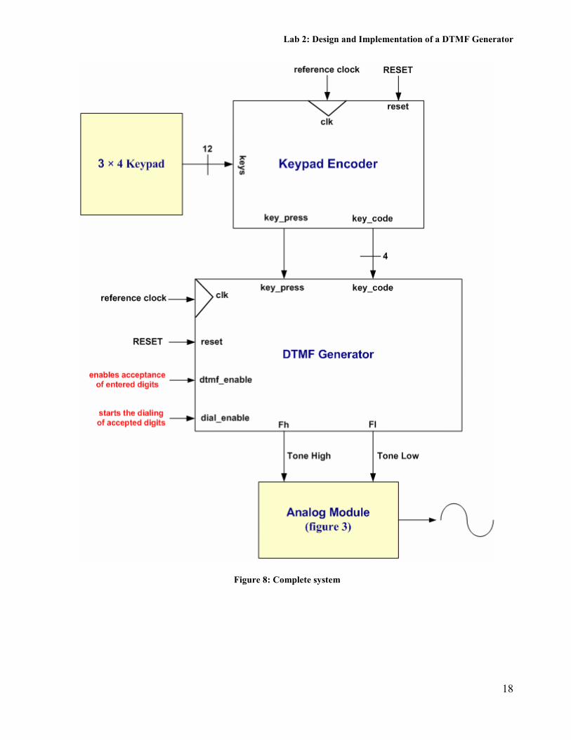
11. Attach the analog modules(keypad + 40-pin ribbon cable circuit, and circuit from figure 3)
to the system as shown in figure 8 below.
12. Download the digital component of the system to the Spartan 3 FPGA development board.
13. Test your final system using an oscilloscope and a spectrum analyzer.
a. Test that the digital component of the system produces both dual tones using a
‘storage oscilloscopes’. Document all results obtained. Photographs of the
oscilloscope screen will be ideal. [2 marks]
b. Test that the analog circuit of figure 3 converts the dual tones to a sinusoidal
waveform. Document all results obtained. Photographs of the oscilloscope screen
will be ideal. [2 marks]
Lab 2: Design and Implementation of a DTMF Generator
18
Figure 8: Complete system

Lab 2: Design and Implementation of a DTMF Generator
19
Design Port FPGA Pin to be mapped to
clk T9
reset any available pushbutton
dtmf_enable any available switch
dtmf_dial any available switch
Fh any available pin
Fl any available pin
keys(0) D11
keys(1) R10
keys(2) C12
keys(3) T7
keys(4) D12
keys(5) R7
keys(6) E11
keys(7) N6
keys(8) B16
keys(9) M6
keys(10) R3
keys(11) C15
Table 2: Pin Configuration for the Keypad Encoder system
Proceed to post-lab exercise.

Lab 2: Design and Implementation of a DTMF Generator
20
5. POST-LAB
A signed plagiarism declaration form must be submitted with your assignment.
Due Date: Friday 27th March 2009
Submission
Procedure: • Students must submit both hard-copies and soft-copies of their report. A
soft-copy of the project folder for the DTMF Generator must also be
submitted.
• Reports must be submitted to Mr. Marcus George in the Electronics
Laboratory.
Deliverables: • Students are expected to produce an informal report on the entire lab
exercise(from pre-lab to post-lab exercise).
• Please organize your report in sections so that it is easy to read and assess.
1. Abstract [3 marks]
2. Pre-lab Exercise [8 marks]
o Answer question asked in pre-lab exercise in the order given
o Students must show all working for calculations done.
3. In-lab Exercise [35 marks]
o Answer question asked in in-lab exercise in the order given
o Students must give a description of the design approach used for all
modules implemented.
o Students must separately describe how smaller modules were
integrated to form the complete system.
o Students must provide functional & timing simulation where
required/asked.
4. Post-lab Exercise [6 marks as stated below]
5. Conclusion [3 marks]
• Demonstration of Working System [5 marks]
Students must demonstrate the working system to the teaching assistant
at anytime before the commencement of laboratory exercise 3. The goal
is to prove that your system is working, through the demonstration of
simulations and use of laboratory equipment. Groups must contact the
teaching assistant when they are ready to demonstrate their system.
Demonstration marks will not be awarded unless students
demonstrate their work.
Students are urged to submit responses to questions asked in this laboratory
exercise in the order of appearance in order to ease marking and ensure
thorough marking of reports.

Lab 2: Design and Implementation of a DTMF Generator
21
Assignment:
1. Suggest and explain an approach that can be used to upgrade the DTMF generator
implemented in this lab to a DMTF generator with the feature of re-dial. This means that
the last number dialed can be re-dialed if requested (probably by the press of a
pushbutton). [4 marks]
2. Develop the datapath block diagram for your approach for the DTMF generator with
redial. [2 marks]
End of Lab 2: Design and Implementation of a DTMF Generator

Lab 2: Design and Implementation of a DTMF Generator
22