ecen689: special topics in high-speed links circuits...
TRANSCRIPT

Sam PalermoAnalog & Mixed-Signal Center
Texas A&M University
ECEN689: Special Topics in High-Speed Links Circuits and Systems
Spring 2010
Lecture 27: PLL Circuits

Announcements
• Project Preliminary Report #1 due now
• Exam 2 is still April 30
• Reading• Posted clocking papers• Website additional links has PLL and jitter
tutorials
• Majority of today’s material from Fischettetutorial and M. Mansuri’s PhD thesis (UCLA)
2

Agenda
• PLL noise transfer functions
• PLL circuits
3
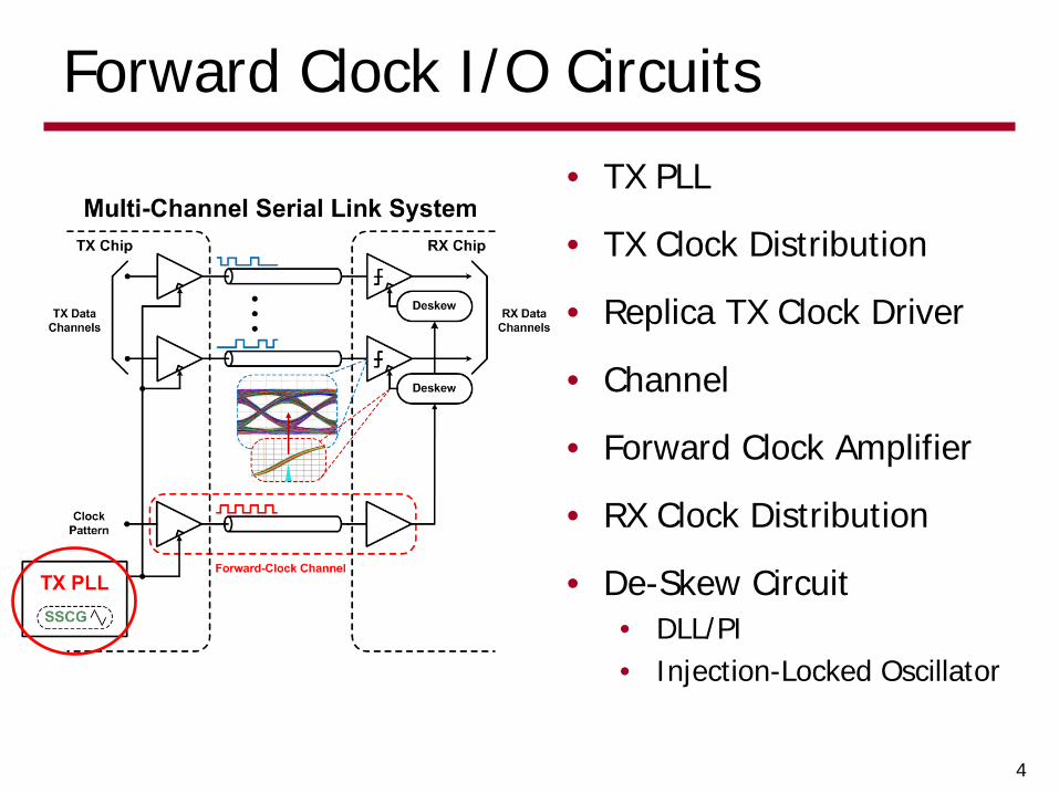
Forward Clock I/O Circuits
4
• TX PLL
• TX Clock Distribution
• Replica TX Clock Driver
• Channel
• Forward Clock Amplifier
• RX Clock Distribution
• De-Skew Circuit• DLL/PI• Injection-Locked Oscillator
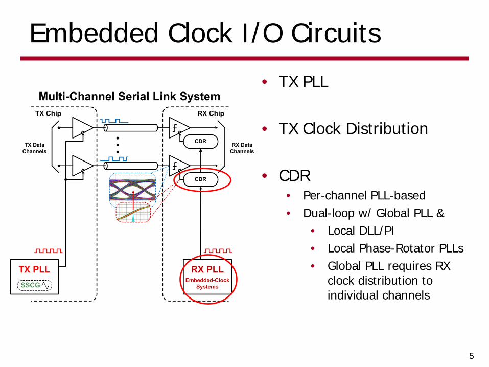
Embedded Clock I/O Circuits
5
• TX PLL
• TX Clock Distribution
• CDR• Per-channel PLL-based• Dual-loop w/ Global PLL &
• Local DLL/PI• Local Phase-Rotator PLLs• Global PLL requires RX
clock distribution to individual channels

Input Noise Transfer Function
6
( ) ( ) ( )22
2
2 221
nn
nn
LoopLoop
Loop
n
outn ss
sN
NK
RCsN
Ks
RCsKsH
IN
IN ωζωωζω
φφ
+++
=+
+
+==
( ) ( )
+
+
+=
==
NK
RCsN
Kss
RCsKKs
Kv
sTLoopLoop
Loopoo
n
out
n
outn
ININ
IN
2
1φφφ
sKo
Input Phase Noise:
Voltage Noise on Input Clock Source:
[Mansuri]

VCO Noise Transfer Function
7
( ) 22
2
2
2
2 nnLoopLoopn
outn ss
s
NK
RCsN
Ks
ssHVCO
VCO ωζωφφ
++=
+
+
==
( )
NK
RCsN
Ks
sKs
Kv
sTLoopLoop
VCOVCO
n
out
n
outn
VCOVCO
VCO
+
+
=
==
2φφφ
VCO Phase Noise:
Voltage Noise on VCO Inputs:
KVCO is different if the input is at the Vcntrl input (KVCO) or supply (KVdd)
[Mansuri]

Clock Buffer Noise Transfer Function
8
( ) 22
2
2
2
2 nnLoopLoopn
outn ss
s
NK
RCsN
Ks
ssHbuf
buf ωζωφφ
++=
+
+
==
( )
NK
RCsN
Ks
sK
NK
RCsN
Ks
ss
Ks
Kv
sTLoopLoop
VCOdelay
LoopLoop
buf
VCOdelay
buf
VCOdelay
n
out
n
outn
bufbuf
buf
+
+
≈+
+
+=
+
==
2
2
2
2
11
ω
ω
ω
ω
ωφφφ
Output Phase Noise:
Voltage Noise on Buffer Inputs:
Kdelay units = (s/V)
[Mansuri]

Noise Transfer Functions
9
[Mansuri]
Input phase noise (N=1) (low-pass)
VCO input voltage noise (band-pass)
Buffer phase or voltage noise (high-pass)
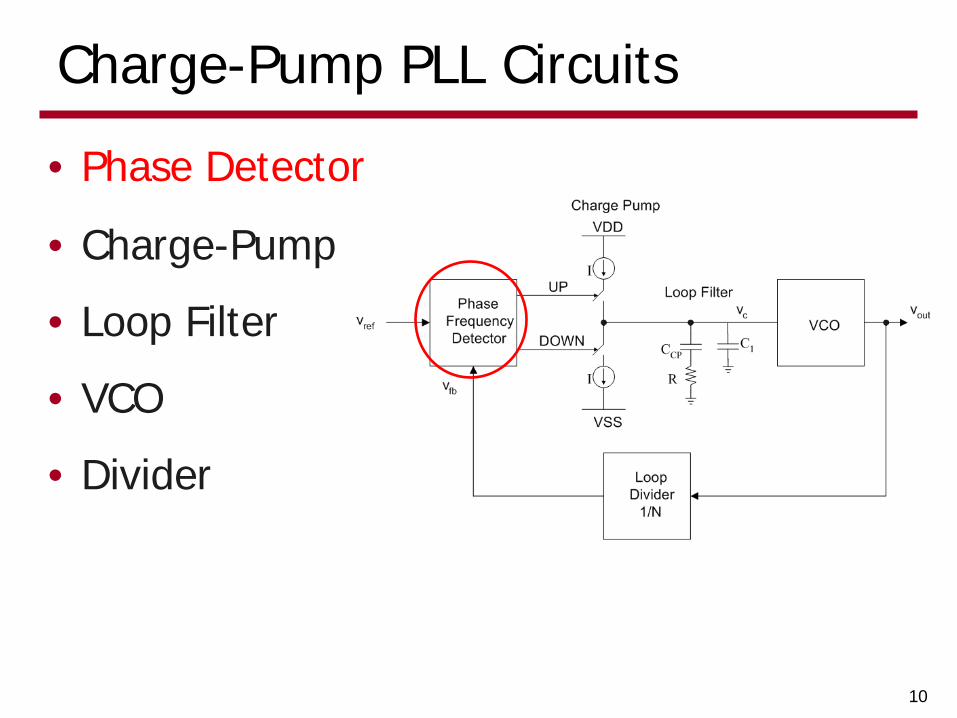
Charge-Pump PLL Circuits
• Phase Detector
• Charge-Pump
• Loop Filter
• VCO
• Divider
10
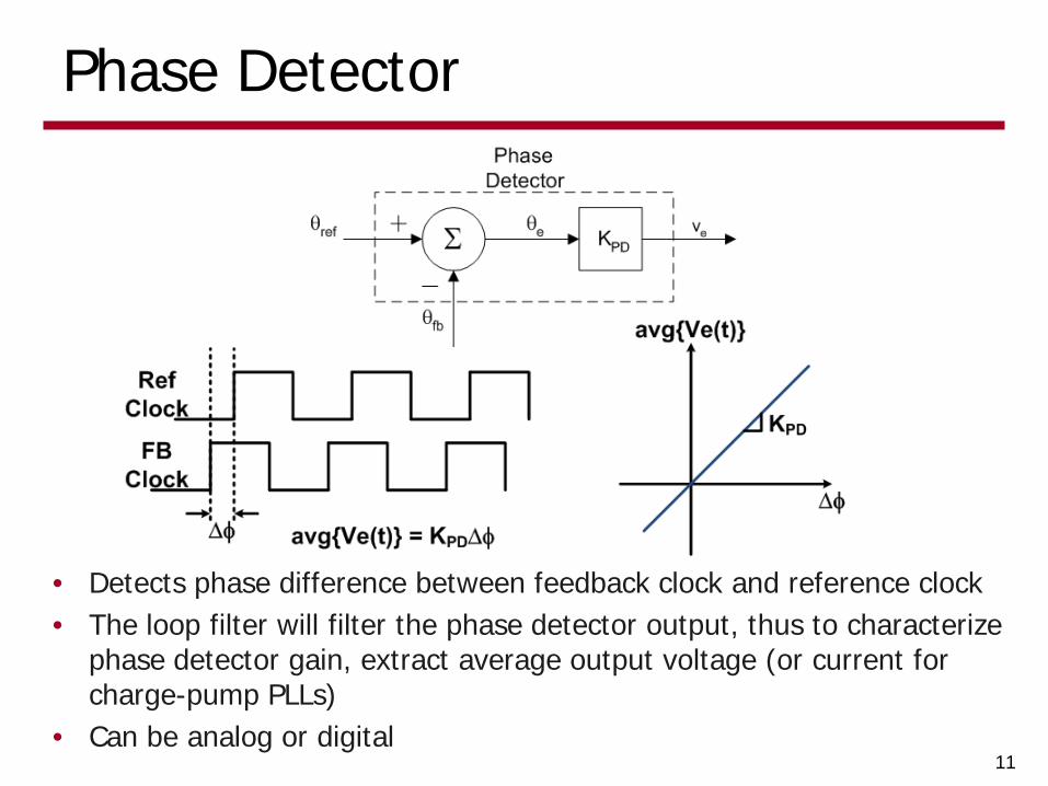
Phase Detector
• Detects phase difference between feedback clock and reference clock• The loop filter will filter the phase detector output, thus to characterize
phase detector gain, extract average output voltage (or current for charge-pump PLLs)
• Can be analog or digital11
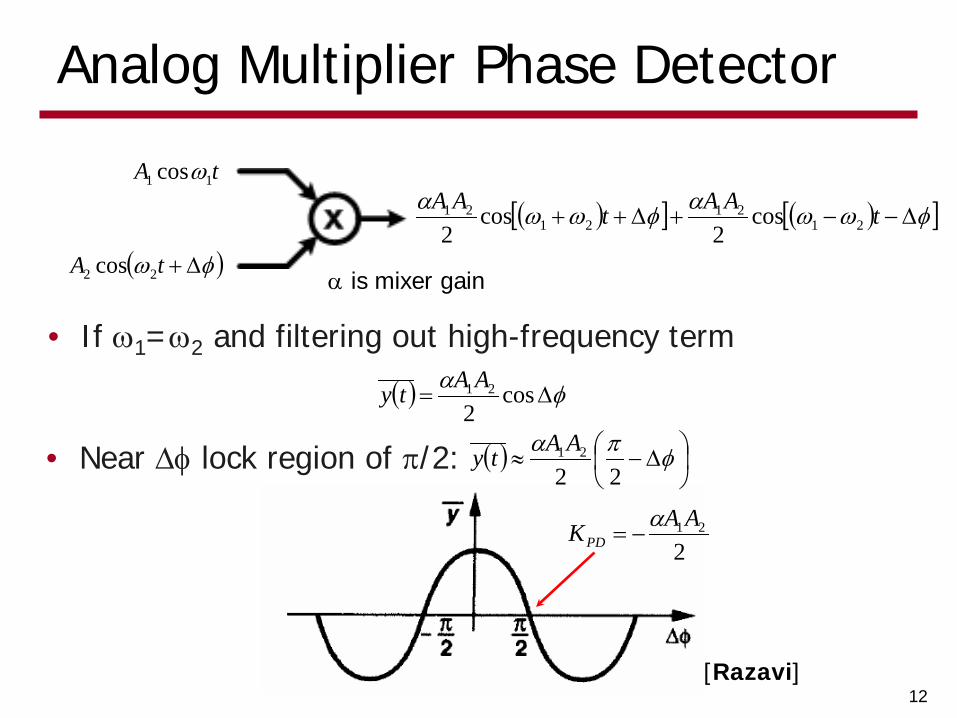
Analog Multiplier Phase Detector
• If ω1=ω2 and filtering out high-frequency term
12
tA 11 cosω
( )φω ∆+tA 22 cos
( )[ ] ( )[ ]φωωαφωωα∆−−+∆++ tAAtAA
2121
2121 cos
2cos
2
α is mixer gain
( ) φα∆= cos
221AAty
• Near ∆φ lock region of π/2: ( )
∆−≈ φπα
2221AAty
221AAKPD
α−=
[Razavi]

XOR Phase Detector
13
• Sensitive to clock duty cycle[Razavi]

XOR Phase Detector
14
[Perrott]

Cycle Slipping
• If there is a frequency difference between the input reference and PLL feedback signals the phase detector can jump between regions of different gain• PLL is no longer acting as a linear system
15
[Perrott]
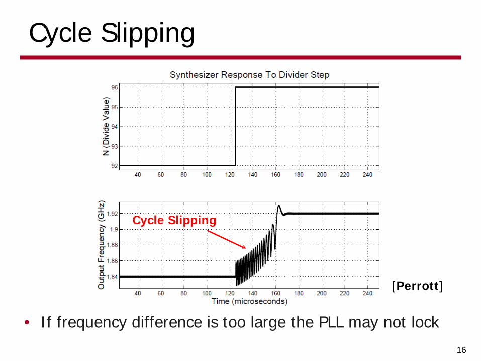
Cycle Slipping
• If frequency difference is too large the PLL may not lock
16
[Perrott]
Cycle Slipping

Phase Frequency Detector (PFD)
• Phase Frequency Detector allows for wide frequency locking range, potentially entire VCO tuning range
• 3-stage operation with UP and DOWN outputs
• Edge-triggered results in duty cycle insensitivity
17

PFD Transfer Characteristic
• Constant slope and polarity asymmetry about zero phase allows for wide frequency range operation
18
UP=1 & DN=-1
[Perrott]

PFD Deadzone• If phase error is small, then short output pulses are produced by PFD• Cannot effectively propagate these pulses to switch charge pump• Results in phase detector “dead zone” which causes low loop gain and
increased jitter• Solution is to add delay in PFD reset path to force a minimum UP and
DOWN pulse length
19
[Fischette]

PFD Operation
20
[Fischette]
Min. Pulse Width

Charge-Pump PLL Circuits
• Phase Detector
• Charge-Pump
• Loop Filter
• VCO
• Divider
21

Charge Pump
• Converts PFD output signals to charge• Charge is proportional to PFD pulse widths
22
I
I
VCO ControlVoltage
C1
R
C2
Charging
Discharging
VDD
VSS
UP
DOWN
CPI
π21
PFD-CP Gain:
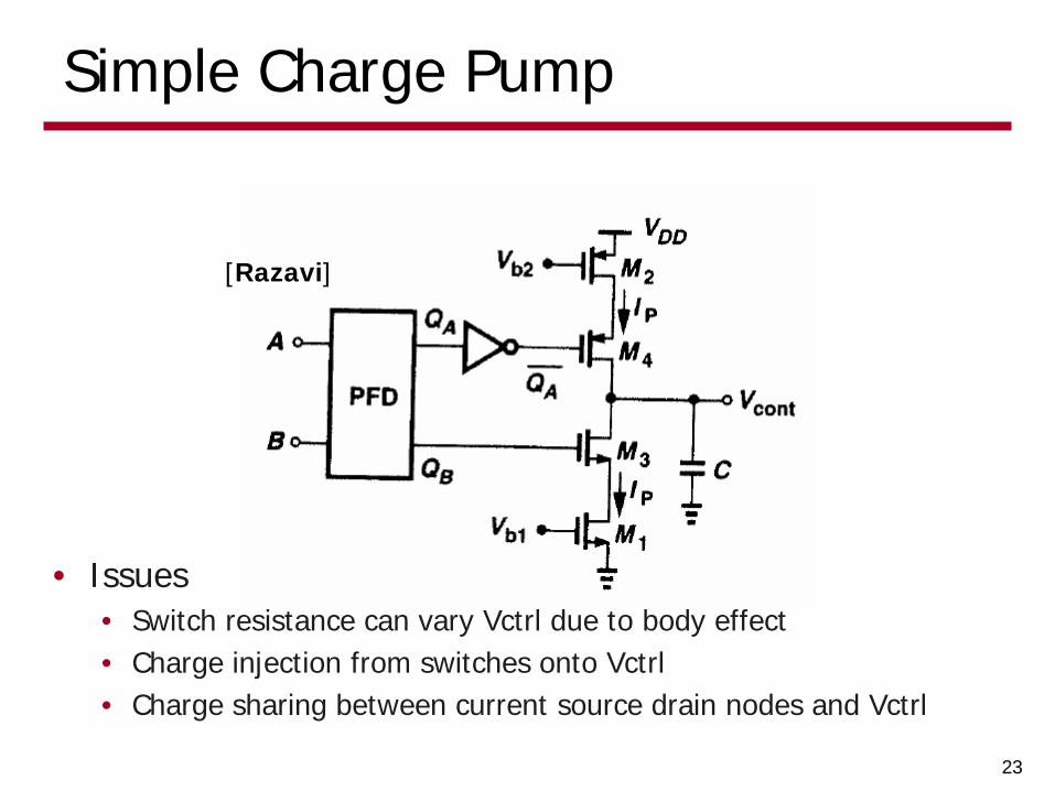
Simple Charge Pump
• Issues• Switch resistance can vary Vctrl due to body effect• Charge injection from switches onto Vctrl• Charge sharing between current source drain nodes and Vctrl
23
[Razavi]

Charge Pump Mismatch
• PLL will lock with static phase error• Extra “ripple” on Vctrl
• Results in frequency domain spurs at the reference clock frequency offset from the carrier
24
[Razavi]

Charge Pump w/ Improved Matching
• Amplifier keeps current source Vds voltages constant resulting in reduced transient current mismatch
25
[Young JSSC 1992]
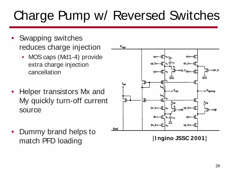
Charge Pump w/ Reversed Switches
• Swapping switches reduces charge injection• MOS caps (Md1-4) provide
extra charge injection cancellation
• Helper transistors Mx and My quickly turn-off current source
• Dummy brand helps to match PFD loading
26
[Ingino JSSC 2001]

Charge-Pump PLL Circuits
• Phase Detector
• Charge-Pump
• Loop Filter
• VCO
• Divider
27
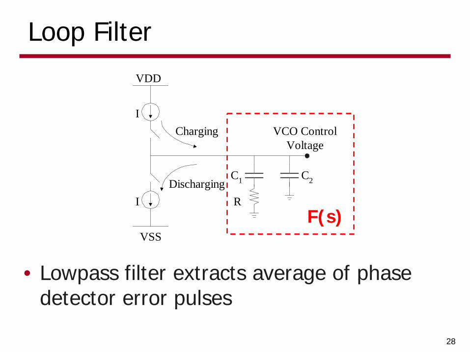
Loop Filter
• Lowpass filter extracts average of phase detector error pulses
28
I
I
VCO ControlVoltage
C1
R
C2
Charging
Discharging
VDD
VSSF(s)

Loop Filter Transfer Function
29
• Neglecting secondary capacitor, C2

Loop Filter Transfer Function
30
• With secondary capacitor, C2

Why have C2?
• Secondary capacitor smoothes control voltage ripple• Can’t make too big or loop will go unstable
• C2 < C1/10 for stability• C2 > C1/50 for low jitter
31
Control Voltage Ripple
Filter Capacitors
• To minimize area, we would like to use highest density caps
• Thin oxide MOS cap gate leakage can be an issue• Similar to adding a non-linear parallel resistor to the capacitor• Leakage is voltage and temperature dependent• Will result in excess phase noise and spurs
• Metal caps or thick oxide caps are a better choice• Trade-off is area
• Metal cap density can be < 1/10 thin oxide caps
• Filter cap frequency response can be relatively low, as PLL loop bandwidths are typically 1-50MHz
32

Charge-Pump PLL Circuits
• Phase Detector
• Charge-Pump
• Loop Filter
• VCO
• Divider
33

Voltage-Controlled Oscillator
• Time-domain phase relationship
34
VDDVDD/20
ω0 1KVCO
( ) ( ) ( )tvKtt cVCOoutout +=∆+= 00 ωωωω
( ) ( ) ( )∫ ∫=∆= dtdt tvKtt cVCOoutout ωθLaplace Domain Model

Voltage-Controlled Oscillators (VCO)
• Ring Oscillator• Easy to integrate• Wide tuning range (5x)• Higher phase noise
• LC Oscillator• Large area• Narrow tuning range (20-30%)• Lower phase noise
35

Barkhausen’s Oscillation Criteria
• Sustained oscillation occurs if
• 2 conditions:• Gain = 1 at oscillation frequency ω0
• Total phase shift around loop is n360° at oscillation frequency ω0
36
( )( )ωωjH
jH−1Closed-loop transfer function:
( ) 1=ωjH
n
[Sanchez]

Ring Oscillator Example
37
[Sanchez]

Ring Oscillator Example
38
[Sanchez]
• 4-stage oscillator• A0 = sqrt(2)• Phase shift = 45
• Easier to make a larger-stage oscillator oscillate, as it requires less gain and phase shift per stage
Next Time
• PLL wrap-up• CDRs
39