dynamic partial reconfigurable hardware architecture for
TRANSCRIPT

RESEARCH Open Access
Dynamic partial reconfigurable hardwarearchitecture for principal componentanalysis on mobile and embedded devicesS. Navid Shahrouzi and Darshika G. Perera*
Abstract
With the advancement of mobile and embedded devices, many applications such as data mining have found theirway into these devices. These devices consist of various design constraints including stringent area and powerlimitations, high speed-performance, reduced cost, and time-to-market requirements. Also, applications running onmobile devices are becoming more complex requiring significant processing power. Our previous analysis illustratedthat FPGA-based dynamic reconfigurable systems are currently the best avenue to overcome these challenges. In thisresearch work, we introduce efficient reconfigurable hardware architecture for principal component analysis (PCA), awidely used dimensionality reduction technique in data mining. For mobile applications such as signature verificationand handwritten analysis, PCA is applied initially to reduce the dimensionality of the data, followed by similaritymeasure. Experiments are performed, using a handwritten analysis application together with a benchmark dataset, toevaluate and illustrate the feasibility, efficiency, and flexibility of reconfigurable hardware for data mining applications.Our hardware designs are generic, parameterized, and scalable. Furthermore, our partial and dynamic reconfigurablehardware design achieved 79 times speedup compared to its software counterpart, and 71% space saving comparedto its static reconfigurable hardware design.
Keywords: Data mining, Embedded systems, FPGAs, Mobile devices, Partial and dynamic reconfiguration,Principal component analysis, Reconfigurable hardware
1 IntroductionWith the proliferation of mobile and embedded comput-ing, a wide variety of applications are becoming commonon these devices. This has opened up research and investi-gation into lean code and small footprint hardware andsoftware architectures. However, these devices havestringent area and power limitations, lower cost and time-to-market requirements. These design constraints poseserious challenges to the embedded system designers.Data mining is one of the many applications that are
becoming common on mobile and embedded devices.Originally limited to a few applications such as scientificresearch and medical diagnosis, data mining has becomevital to a variety of fields including finance, marketing,security, biotechnology, and multimedia. Many of today’sdata mining tasks are compute and data intensive,
requiring significant processing power. Furthermore, inmany cases, the data need to be processed in real timeto reap the actual benefits. These constraints have alarge impact on the speed-performance of the applica-tions running on mobile devices.To satisfy the requirements and constraints of the mo-
bile and embedded devices, and also to enhance thespeed-performance of the applications running on thesedevices, it is imperative to incorporate some special-purpose hardware into embedded system designs. Thesecustomized hardware algorithms should be executed insingle-chip systems, since multi-chip solutions might notbe suitable due to the limited footprint on mobile andembedded devices. The customized hardware provides su-perior speed-performance, lower power consumption, andarea efficiency [12, 40], compared to the equivalent softwarerunning on general-purpose microprocessor, advantagesthat are crucial for mobile and embedded devices.* Correspondence: [email protected]
Department of Electrical and Computer Engineering, University of Colorado,1420 Austin Bluffs Parkway, Colorado Springs, CO 80918, USA
EURASIP Journal onEmbedded Systems
© The Author(s). 2017 Open Access This article is distributed under the terms of the Creative Commons Attribution 4.0International License (http://creativecommons.org/licenses/by/4.0/), which permits unrestricted use, distribution, andreproduction in any medium, provided you give appropriate credit to the original author(s) and the source, provide a link tothe Creative Commons license, and indicate if changes were made.
Shahrouzi and Perera EURASIP Journal on Embedded Systems (2017) 2017:25 DOI 10.1186/s13639-017-0074-x
For more complex operations, it might not be possibleto populate all the computation circuitry into a singlechip. An alternative is to take the advantage of reconfig-urable computing systems. Reconfigurable hardware hassimilar advantages as special-purpose hardware, leadingto low power and high performance. Furthermore, re-configurable computing systems have added advantages:a single chip to perform the required operation, flexiblecomputing platform, and reduced time-to-market. Thisreconfigurable computing system could address theconstraints associated with mobile and embeddeddevices, as well as the flexibility and performance issuesin processing a large data set.In [30], an analysis of single-chip hardware support for
mobile and embedded applications was carried out.These analyses illustrated that FPGA-based reconfigur-able hardware provides numerous advantages, includingflexibility, upgradeability, compact circuits and area effi-ciency, shorter time-to-market, and relatively low cost,which are important for mobile and embedded devices.Multiple applications can be executed on a single chip,by dynamically reconfiguring the hardware on chip fromone application to another as needed.Our main objective is to provide efficient dynamic
reconfigurable hardware architectures for data miningapplications on mobile and embedded devices. In thisresearch work, we focus on reconfigurable hardwaresupport for dimensionality reduction techniques in datamining, specifically principal component analysis (PCA).For mobile applications such as signature verificationand handwritten analysis, PCA is applied initially toreduce the dimensionality of the data, followed bysimilarity measure.This paper is organized as follows: In Section 2, we
discuss and present the main tasks in data mining, issuesin mining high-dimensional data, and elaborate onprincipal component analysis (PCA), one of the mostcommonly used dimensionality reduction techniques indata mining. Our design approach and developmentplatform are presented in Section 3. In Section 4, thepartial and dynamic reconfigurable hardware architec-ture for the four stages of the PCA algorithm is intro-duced. Experiments are carried out to evaluate thespeed-performance and area efficiency of the reconfigur-able hardware designs. These experimental results andanalysis are reported and discussed in Section 5. In Sec-tion 6, we summarize our work and conclude.
2 Data mining techniquesData mining is an important research area as many ap-plications in various domains can make use of it to sievethrough large volume of data to discover useful patternsand valuable knowledge. It is a process of finding corre-lations or patterns among various fields in large data
sets; this is done by analyzing the data from many differ-ent perspectives, categorizing it, and summarizing theidentified relationships [6].Data mining commonly involves any of the four main
high-level tasks [15, 28]: classification, clustering, regression,and association rule mining. From these, we are focusing onthe mostly widely used clustering and classification, whichtypically involves the following steps [15, 28]: patternrepresentation, pattern proximity measure, grouping (forclustering) and labeling (for classifying), and data abstrac-tion (optional).Pattern representation is the first step toward clustering
or classification. Patterns (or records) are represented asmultidimensional vectors, where each dimension (orattribute) represents a single feature [34]. Patternrepresentation is often used to extract the most descriptiveand discriminatory features in the original data set; thenthese features can be used exclusively in subsequentanalyses [22].
2.1 Mining high-dimensional dataAn important issue often arises, while clustering orclassifying, is the problem of having too many attri-butes (or dimensions). There are four major issuesassociated with clustering or classifying high-dimensionaldata [4, 15, 24]:
� Multiple dimensions are impossible to visualize.Also, since the amount of data often increasesexponentially with dimensionality, multipledimensions are becoming increasingly difficult toenumerate [24]. This is known as curse ofdimensionality [24].
� As the number of dimensions increase, the conceptof proximity or distance becomes less precise; this isespecially true for spatial data [13].
� Clustering typically group objects that are relatedbased on the attribute’s value. When there is a largenumber of attributes, it is highly likely that some ofthe attributes or features might be irrelevant, thusnegatively affects the proximity measures and thecreation of clusters [4, 24].
� Correlations among subsets of features: When thereis a large number of attributes, it is highly likely thatsome of the attributes are correlated [24].
To overcome the above issues, pattern representationtechniques such as feature extraction and feature selec-tion are often used to reduce the dimensionality beforeperforming any other data mining tasks.Some of the feature selection methods used for dimen-
sionality reduction include mutual information [28], chi-square [28], and sensitivity analysis [1, 56]. Some of thefeature extraction methods used for dimensionality
Shahrouzi and Perera EURASIP Journal on Embedded Systems (2017) 2017:25 Page 2 of 18
reduction include singular value decomposition [14, 37],principal component analysis [21, 23], independentcomponent analysis [20], and factor analysis [7].
2.2 PCA: a dimensionality reduction techniqueAmong the feature extraction/selection methods, prin-cipal component analysis (PCA) is the most commonly[1, 23, 37] used dimensionality reduction technique inclustering and classification problems. In addition, due tothe necessity of having a small memory footprint of data,PCA is applied to many data mining applications that areappropriate for mobile and embedded devices such as:handwritten analysis or signature verification, palm-printor finger-print verification, iris verification, and facialrecognition.PCA is a classical technique [42]: The main idea is to ex-
tract the prominent features of the data set and to performdata reduction (compression). PCA finds a linear transform-ation, known as Karhunen-Loeve Transform (KLT), whichreduces the number of the dimensions of the feature vectorsfrom m to d (where d < <m) in such a way that the “infor-mation is maximally preserved in minimum mean squarederror sense” [11, 36]. PCA reduces the dimensionality of thedata by transforming the original data set to a new set ofvariables called principal components (PCs) to extract theprominent features of the data [23, 42]. According to Yeungand Ruzzo [57], “PCs are uncorrelated and ordered, suchthat the kth PC has kth largest variance among all PCs; andthe kth PC can be interpreted as the direction that maxi-mizes the variation of the projection of the data pointssuch that it is orthogonal to the first (k-1) PCs.” Tradition-ally, the first few PCs are used in data analysis, since theyretain most of the variants among the data features (inthe original data set), and eliminate (by the projection)those features that are highly correlated among them-selves; whereas the last few PCs are often assumed toretain only the residual noise in the data [23, 57].Since PCA effectively reduces the dimensionality of
the data, the main advantage of applying PCA on ori-ginal data is to reduce the size of the computationalproblem [42]. Normally, when the number of attributesof a data set is large, it takes more time to process thedata, since the number of attributes is directly propor-tional to processing time; thus, by reducing the numberof attributes (dimensions), running time of the systemcan be minimized [42]. In addition, for clustering, ithelps to identify the characteristics of the clusters [22],and for classification, it improves classification accuracy[1, 56]. The main disadvantage of applying PCA is theloss of information, since there is no guarantee that thesacrificed information is not relevant to the aims offurther studies, and also there is no guarantee that thelargest PCs obtained will contain good features forfurther analysis [21, 57].
2.2.1 The process of PCAPCA computation consists of four stages [21, 37, 38]:mean computation, covariance matrix computation,eigenvalue matrix, thus eigenvector computation, andPCs matrix computation. Consider the original inputdata set {X}mXn as an mXn matrix, where m is the num-ber of dimensions and n is the number of vectors.Firstly, the mean is computed along the dimensions ofthe vectors of the data set. Secondly, the covariancematrix is computed after determining the deviation fromthe mean. Covariance is always measured between twodimensions [21, 38]. With covariance, one can find outhow much the dimensions vary from the mean withrespect to each other [21, 38]. Covariance between onedimension and itself gives the variance.Thirdly, eigenanalysis is performed on the covariance
matrix to extract independent orthonormal eigenvaluesand eigenvectors [2, 21, 37, 38]. As stated in [2, 38],eigenvectors are considered as the “preferential directions”or the main patterns in the data, and eigenvalues areconsidered as the quantitative assessment of how much aPC represents the data. Eigenvectors with the highesteigenvalues correspond to the variables (dimensions) withthe highest correlation in the data set. Lastly, the set ofPCs is computed and sorted by their eigenvalues indescending order of significance [21].Various techniques can be used to perform PCA
computation. These techniques typically depend on theapplication and the data set used. The most commonalgorithm for PCA involves the computation of the eigen-value decomposition of a covariance matrix [21, 37, 38].There are also various ways of performing eigenanalysis oreigenvalue decomposition (EVD). One well known EVDmethod is cyclic Jacobi method [14, 33]. However, this isonly suitable for small matrices, where number ofdimensions are less than or equal to 10 (m = <10) [14, 37].For larger matrices [29], where the number of dimensionsare more than 10 (m > 10), other algorithms such as QR[1, 56], Householder [29], or Hessenberg [29] methodsshould be employed. Among these methods, QR algo-rithm, first introduced in 1961, is one of the most efficientand accurate methods to compute eigenvalues andeigenvectors during PCA analysis [29, 41]. It can simul-taneously approximate all the eigenvalues of a matrix. Forour work, we are using QR algorithm for EVD.In summary, clustering and classifying high-dimensional
data presents many challenging problems in this big dataera. The computational cost of processing massiveamount of data in real time is immense. PCA can reducea complex high-dimensional data set to a lower dimen-sion, in order to unveil the simplified structures that areotherwise hidden, while reducing the size of the computa-tional cost of analyzing the data [21, 37, 38]. Hardwaresupport could further reduce the computational cost of
Shahrouzi and Perera EURASIP Journal on Embedded Systems (2017) 2017:25 Page 3 of 18

processing data and improve the speed-performance ofthe PCA analysis. In this research work, we introducepartial and dynamic reconfigurable hardware to enhancethe PCA computation for mobile and embedded devices.
3 Design approach and development platformFor all our experiments, both software and hardwareversions of the various computations are implementedusing a hierarchical platform-based design approach tofacilitate component reuse at different levels of abstrac-tion. The hardware versions include static reconfigurablehardware (SRH) and dynamic reconfigurable hardware(DRH). As shown in Fig. 1, our design consists of differ-ent abstraction levels, where higher-level functions uti-lizes lower-level sub-functions and operators: thefundamental operators including add, multiply, subtract,compare, square-root, and divide at the lowest level;mean, covariance matrix, eigenvalue matrix, and PCmatrix computations at the next level; and the PCA atthe highest level.All our hardware and software experiments are carried
out on the ML605 FPGA development board [51], whichis built on a 40-nm CMOS process technology. TheML605 board utilizes a Xilinx Virtex 6 XC6VLX240T-FF1156 device. The development platform includes largeon-chip logic resources (37,680 slices), MicroBlaze softprocessors, and onboard configuration circuitry fordevelopment purpose. It also includes 2-MB on-chipBRAM (block random access memory) and 512-MBDDR3-SDRAM external memory to hold large volumeof data. To hold the configuration bitstreams, ML605
board has several external non-volatile memories includ-ing 128 MB of Platform Flash XL, 32-MB BPI LinearFlash, and 2-GB Compact Flash. Additional user desiredfeatures could be added through daughter cards attachedto the two onboard FMC (FPGA Mezzanine Connectors)expansion connectors.Both the static and dynamic reconfigurable hardware
modules are designed in mixed VHDL and Verilog. Theyare executed on the FPGA (running at 100 MHz) toverify their correctness and performance. Xilinx ISE 14.7and XPS 14.7 are used for the SRH designs. Xilinx ISE14.7, XPS 14.7, and PlanAhead 14.7 (with partial recon-figuration features) are used for the DRH designs.ModelSim SE and Xilinx ChipscopePro 14.7 are used toverify the results and functionalities of the designs.Software modules are written in C and executed on theMicroBlaze processor (running at 100 MHz) on thesame FPGA with level-II optimization. Xilinx XPS 14.7and SDK 14.7 are used to verify the software modules.As a proof-of-concept work [31, 32], we initially pro-
posed reconfigurable hardware support for the first twostages of the PCA computation, where both the SRH[31] and the DRH [32] are designed using integer opera-tors. Unlike our proof-of-concept designs, in this re-search work, both the software and hardware modulesare designed using floating-point operators, instead ofinteger operators. The hardware modules for the funda-mental operators are designed using single precisionfloating-point units [50] from the Xilinx IP core library.The MicroBlaze is also configured to use single precisionfloating-point unit for the software modules.
Fig. 1 Hierarchical platform-based design approach. Our design consists of different abstraction levels, where higher-level functions utilizelower-level sub-functions
Shahrouzi and Perera EURASIP Journal on Embedded Systems (2017) 2017:25 Page 4 of 18
The performance gain or speedup resulting from theuse of hardware over software is computed using thefollowing formula:
Speedup ¼ BaselineExecutionTime Softwareð ÞImprovedExecutionTime Hardwareð Þ
ð1Þ
Since our intention is to provide reconfigurable hard-ware architectures for data mining applications on mo-bile and embedded devices, we decided to utilize a dataset that is appropriate for applications on these devices.After exploring several databases, we decided on a realbenchmark data set, the “Optdigit” [3], for recognizinghandwritten characters. The database consists of 200handwritten characters from 43 people. The data set has3823 records (vectors), where each record has 64 attri-butes (elements). We investigated several papers thatused this data set for PCA computations and obtainedsource codes written in MatLab for PCA analysis fromone of the authors [39]. Results from the MatLab codeon the optdigit data set are used to verify our resultsusing reconfigurable hardware designs as well as soft-ware designs. In addition, a software program written inC for the PCA computation is executed on a personalcomputer. These results are also used to verify our re-sults from the embedded software and hardware designs.
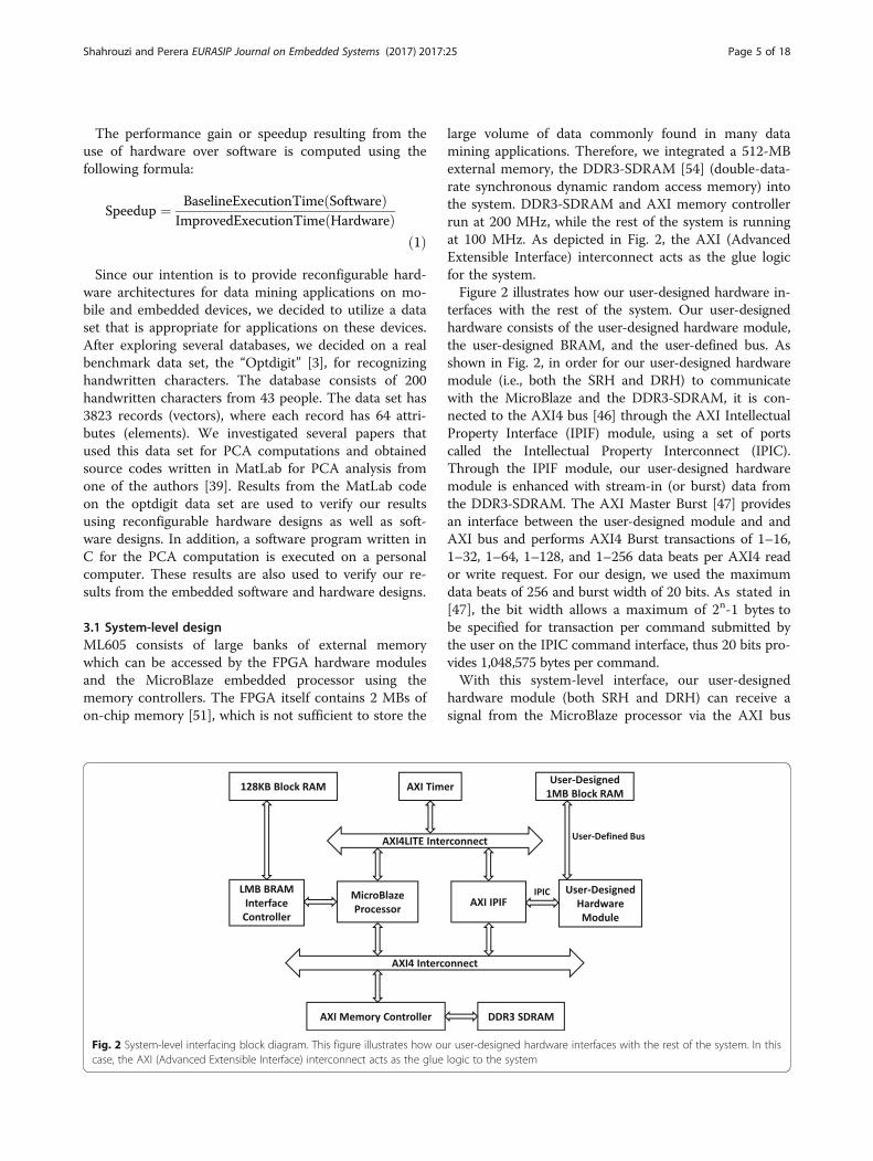
3.1 System-level designML605 consists of large banks of external memorywhich can be accessed by the FPGA hardware modulesand the MicroBlaze embedded processor using thememory controllers. The FPGA itself contains 2 MBs ofon-chip memory [51], which is not sufficient to store the
large volume of data commonly found in many datamining applications. Therefore, we integrated a 512-MBexternal memory, the DDR3-SDRAM [54] (double-data-rate synchronous dynamic random access memory) intothe system. DDR3-SDRAM and AXI memory controllerrun at 200 MHz, while the rest of the system is runningat 100 MHz. As depicted in Fig. 2, the AXI (AdvancedExtensible Interface) interconnect acts as the glue logicfor the system.Figure 2 illustrates how our user-designed hardware in-
terfaces with the rest of the system. Our user-designedhardware consists of the user-designed hardware module,the user-designed BRAM, and the user-defined bus. Asshown in Fig. 2, in order for our user-designed hardwaremodule (i.e., both the SRH and DRH) to communicatewith the MicroBlaze and the DDR3-SDRAM, it is con-nected to the AXI4 bus [46] through the AXI IntellectualProperty Interface (IPIF) module, using a set of portscalled the Intellectual Property Interconnect (IPIC).Through the IPIF module, our user-designed hardwaremodule is enhanced with stream-in (or burst) data fromthe DDR3-SDRAM. The AXI Master Burst [47] providesan interface between the user-designed module and andAXI bus and performs AXI4 Burst transactions of 1–16,1–32, 1–64, 1–128, and 1–256 data beats per AXI4 reador write request. For our design, we used the maximumdata beats of 256 and burst width of 20 bits. As stated in[47], the bit width allows a maximum of 2n-1 bytes tobe specified for transaction per command submitted bythe user on the IPIC command interface, thus 20 bits pro-vides 1,048,575 bytes per command.With this system-level interface, our user-designed
hardware module (both SRH and DRH) can receive asignal from the MicroBlaze processor via the AXI bus
Fig. 2 System-level interfacing block diagram. This figure illustrates how our user-designed hardware interfaces with the rest of the system. In thiscase, the AXI (Advanced Extensible Interface) interconnect acts as the glue logic to the system
Shahrouzi and Perera EURASIP Journal on Embedded Systems (2017) 2017:25 Page 5 of 18

and start processing, read/write data/results from/to theDDR3-SDRAM, and send a signal to the MicroBlazewhen execution is completed. When MicroBlaze sends asignal to the hardware module, it can then continue toexecute other tasks until the hardware module writesback the results to the DDR3-SDRAM and sends asignal to notify the processor. The execution times forthe hardware as well as MicroBlaze are obtained usingthe hardware AXI Timer [49] running at 100 MHz.
3.1.1 Pre-fetching techniqueFrom our proof-of-concept work [32], it was observedthat a significant amount of time was spent on accessingDDR3-SDRAM external memory, which was a majorperformance bottleneck. For the current system-leveldesign, in addition to the AXI Master Burst, we designedand incorporated a pre-fetching technique to our user-designed hardware (in Fig. 2) in order to overcome thismemory access latency issue.The top-level block diagram of our user-designed
hardware is demonstrated in Fig. 3, which consists oftwo separate user-designed IPs. User IP1 consists of theStep X Module (i.e., hardware module designed for eachstage of the PCA computation), the slave registers, andthe Read/Write module; whereas User IP2 consists ofthe BRAM.
User IP1 can communicate with the MicroBlaze pro-cessor using the software accessible registers known asthe slave registers. Each stage of the PCA computation(Step X module) consists of a data path and a controlpath. Both the data and control paths have direct con-nections to the on-chip BRAM via user-defined inter-faces. Within the User IP1, we designed a separate Read/Write (R/W) module to support the pre-fetching tech-nique. The R/W module translates the IPIC signals tothe control path and vice versa, thus reducing the com-plexity of the control path.User IP2 is also designed to support the pre-fetching
technique. User IP2 consists of 1 MB BRAM [45] fromthe Xilinx IP Core library. This dual-port BRAM sup-ports simultaneous read/write capabilities.
3.1.1.1 During the read operation (pre-fetching): Theessential data for a specific computation is pre-fetchedfrom the DDR3-SDRAM to the on-chip BRAM. In thiscase, firstly, the control path sends the read request, thestart address, and the burst length to the R/W module.Secondly, the R/W module asserts the necessary IPICsignals in order to read the data from SDRAM via IPIF.The R/W module waits for the ready-read acknowledg-ment signal from the DDR3-SDRAM. Thirdly, the datais fetched (in burst read transaction mode) from the
Fig. 3 Top-level user-designed hardware block diagram. The top-level module consists of our two user-designed IPs
Shahrouzi and Perera EURASIP Journal on Embedded Systems (2017) 2017:25 Page 6 of 18
SDRAM via R/W module and buffered to the BRAM.During this step, the control path sends the writerequest and the necessary addresses to the BRAM.
3.1.1.2 During the computations: Once the requireddata is available in the BRAM, the data is loaded to thedata path in every clock cycle, and the necessary computa-tions are performed. The control path monitors the datapath and enables appropriate signals to perform the com-putations. The data paths are designed in pipelined fash-ion; hence most of the final and intermediate results arealso produced in every clock cycle and written to theBRAM. Only the final results are written to the SDRAM.
3.1.1.3 During the write operation: In this case also,initially, the control path sends the write request, thestart address, and the burst length to the R/W module.Secondly, the R/W module asserts the necessary IPICsignals in order to write the results to the DDR3-SDRAM via IPIF. The R/W module waits for the ready-write acknowledgment signal from the SDRAM. Thirdly,the data is buffered from the BRAM and forwarded (inburst write transaction mode) to the SDRAM via R/Wmodule. During this step, the control path sends theread request and the necessary addresses to the BRAM.The read/write operations from/to the BRAM are
designed to overlap with the computations by bufferingthe data through the user-defined bus. Our currenthardware designs are fully pipelined, further enhancingthe throughput. All these design techniques led to higherspeed-performance compared to our proof-of-conceptdesigns. These performance analyses are presented inSection 5.2.3.
3.2 Reconfiguration processReconfigurable hardware designs, such as FPGA-baseddesigns, are typically written in a hardware descriptionlanguage (HDL) including Verilog or VHDL [5, 17]. Thisabstract design has to undergo the following consecutivesteps to fit into FPGA’s available logic [17]: The first stepis logic synthesis, which converts high-level logic con-structs and behavioral code into logic gates; the secondstep is technology mapping, which separates the gatesinto groupings that match the FPGA’s logic resources(generates net list); the next two consecutive steps areplacement and routing, where placement allocates thelogic groupings to the specific logic blocks and routingdetermines the interconnect resources that will carry thesignals [17]. The final step is bitstream generation, whichcreates a “configuration bitstream” for programming theFPGA.We can distinguish reconfigurable hardware into two
types: static and dynamic. With static reconfiguration, a fullconfiguration bitstream of an application is downloaded to
the FPGA at system start-up, and the chip is configuredonly once and seldom changed throughout the run-time-life of the application. In order to execute a different appli-cation, a full configuration bitstream of that applicationhas to be downloaded again and the entire chip has to bereconfigured. The system has to be interrupted for everydownload and reconfiguration process. With dynamic re-configuration, a full configuration bitstream of an applica-tion is downloaded to the FPGA at system start-up, andthe on-chip hardware is configured, but is often changedduring the run-time-life of the application. This kind ofreconfiguration allows changing either parts of the chip orthe whole chip as needed on-the-fly, to perform severaldifferent computations without human intervention andin certain scenarios without interrupting the systemoperations.In summary, dynamic reconfiguration has the ability
to perform hardware optimization based upon presentresults or external stimuli determined at run-time. Inaddition, with dynamic reconfiguration, we can run alarge application on a smaller chip by partitioning theapplication into sub-circuits and executing the sub-circuits on chip at different times.
3.2.1 Partial reconfiguration on Virtex 6There are two different reconfiguration methods that canbe used with Virtex-6 FPGAs: MultiBoot and PartialReconfiguration. MultiBoot [19] is a reconfigurationmethod that allows full bitstream reconfiguration, whereaspartial reconfiguration [52] allows partial bitstream recon-figuration. We used partial reconfiguration method forour dynamic reconfigurable hardware design.Dynamic partial reconfiguration allows reconfiguring
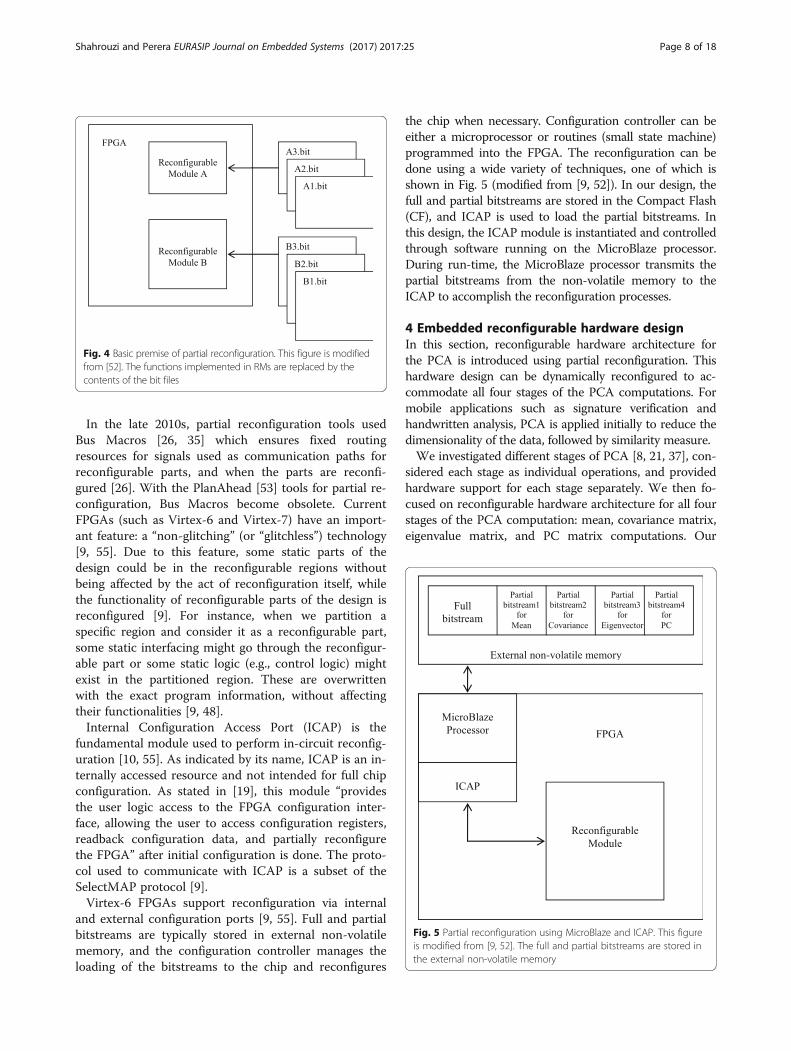
parts of the chip that requires modification, whileinterfacing with the other parts that remain operational[9, 52]. First, the FPGA is configured by loading aninitial full configuration bitstream for the entire chipupon power-up. After the FPGA is fully configured andoperational, multiple partial bitstreams can be down-loaded simultaneously to the chip, and specific regionsof the chip can be reprogrammed with new functionality“without compromising the integrity of the applications”running in the remainder of the chip [9, 52]. Partialbitstreams are used to reconfigure only selective parts ofthe chip. Figure 4, which is modified from [52],illustrates the basic premise of partial reconfiguration.During the design and implementation process, the logicin the reconfigurable hardware design is divided intotwo different parts: reconfigurable and static. As shownin Fig. 4, the functions implemented in reconfigurablemodules (RM), i.e., reconfigurable parts, are replaced bythe contents of the partial bitstreams (.bit files), whilethe current static parts remain operational, completelyunaffected by the reconfiguration [52].
Shahrouzi and Perera EURASIP Journal on Embedded Systems (2017) 2017:25 Page 7 of 18
In the late 2010s, partial reconfiguration tools usedBus Macros [26, 35] which ensures fixed routingresources for signals used as communication paths forreconfigurable parts, and when the parts are reconfi-gured [26]. With the PlanAhead [53] tools for partial re-configuration, Bus Macros become obsolete. CurrentFPGAs (such as Virtex-6 and Virtex-7) have an import-ant feature: a “non-glitching” (or “glitchless”) technology[9, 55]. Due to this feature, some static parts of thedesign could be in the reconfigurable regions withoutbeing affected by the act of reconfiguration itself, whilethe functionality of reconfigurable parts of the design isreconfigured [9]. For instance, when we partition aspecific region and consider it as a reconfigurable part,some static interfacing might go through the reconfigur-able part or some static logic (e.g., control logic) mightexist in the partitioned region. These are overwrittenwith the exact program information, without affectingtheir functionalities [9, 48].Internal Configuration Access Port (ICAP) is the
fundamental module used to perform in-circuit reconfig-uration [10, 55]. As indicated by its name, ICAP is an in-ternally accessed resource and not intended for full chipconfiguration. As stated in [19], this module “providesthe user logic access to the FPGA configuration inter-face, allowing the user to access configuration registers,readback configuration data, and partially reconfigurethe FPGA” after initial configuration is done. The proto-col used to communicate with ICAP is a subset of theSelectMAP protocol [9].Virtex-6 FPGAs support reconfiguration via internal
and external configuration ports [9, 55]. Full and partialbitstreams are typically stored in external non-volatilememory, and the configuration controller manages theloading of the bitstreams to the chip and reconfigures
the chip when necessary. Configuration controller can beeither a microprocessor or routines (small state machine)programmed into the FPGA. The reconfiguration can bedone using a wide variety of techniques, one of which isshown in Fig. 5 (modified from [9, 52]). In our design, thefull and partial bitstreams are stored in the Compact Flash(CF), and ICAP is used to load the partial bitstreams. Inthis design, the ICAP module is instantiated and controlledthrough software running on the MicroBlaze processor.During run-time, the MicroBlaze processor transmits thepartial bitstreams from the non-volatile memory to theICAP to accomplish the reconfiguration processes.
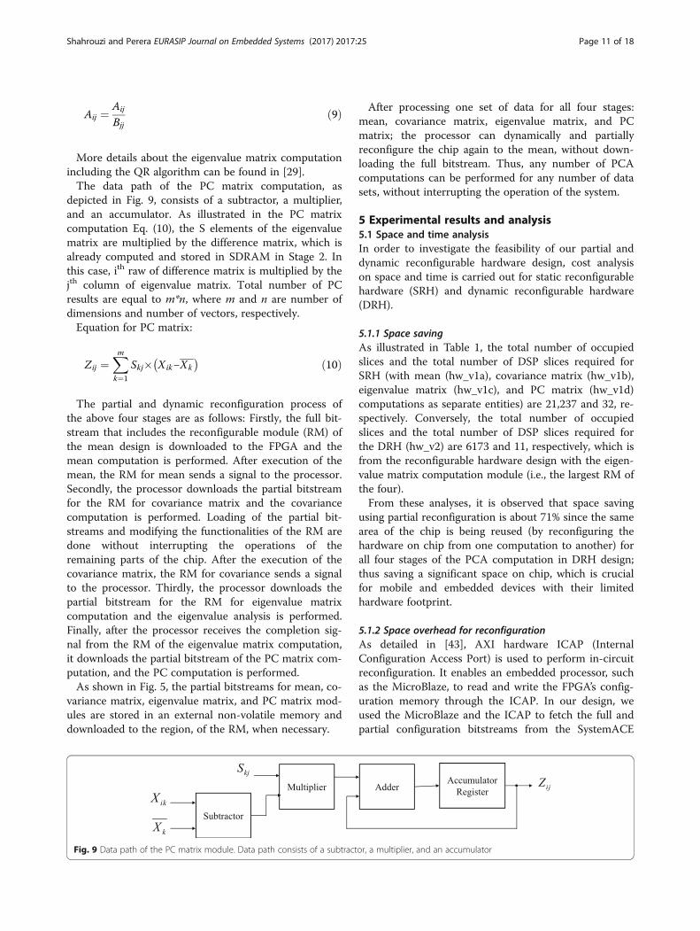
4 Embedded reconfigurable hardware designIn this section, reconfigurable hardware architecture forthe PCA is introduced using partial reconfiguration. Thishardware design can be dynamically reconfigured to ac-commodate all four stages of the PCA computations. Formobile applications such as signature verification andhandwritten analysis, PCA is applied initially to reduce thedimensionality of the data, followed by similarity measure.We investigated different stages of PCA [8, 21, 37], con-
sidered each stage as individual operations, and providedhardware support for each stage separately. We then fo-cused on reconfigurable hardware architecture for all fourstages of the PCA computation: mean, covariance matrix,eigenvalue matrix, and PC matrix computations. Our
Fig. 4 Basic premise of partial reconfiguration. This figure is modifiedfrom [52]. The functions implemented in RMs are replaced by thecontents of the bit files
Fig. 5 Partial reconfiguration using MicroBlaze and ICAP. This figureis modified from [9, 52]. The full and partial bitstreams are stored inthe external non-volatile memory
Shahrouzi and Perera EURASIP Journal on Embedded Systems (2017) 2017:25 Page 8 of 18

hardware design can be reconfigured partially and dynam-ically from one stage to another, in order to perform thesefour operations on the same area of the chip.The equations [21, 37] for mean and covariance matrix
for the PCA computation are as follows:Equation for mean:
Xj ¼Xn
i¼1Xij
nð2Þ
Equation for covariance matrix:
Covij ¼Xn
k¼1Xki−Xi� �
Xkj−Xj� �
n−1ð Þ ð3Þ
For our proof-of-concept work [32], we modified theabove two equations slightly in order to use integeroperations for the mean and covariance matrix compu-tations. It should be noted that we only designed thefirst two stages of the PCA computation in our previouswork [32]. For this research work, we are using singleprecision floating-point operations for all four stages ofthe PCA computations. The reconfigurable hardware de-signs for each stage consist of a data path and a controlpath. Each data path is designed in pipelined fashion;thus, in every clock cycle, the data is processed by onemodule, and the results are forwarded to the nextmodule, and so on. Furthermore, the computations aredesigned to overlap with the memory access to harnessthe maximum benefit of the pipelined design.The data path of the mean, as depicted in Fig. 6, con-
sists of an accumulator and a divider. The accumulatoris designed as a sequence of an adder and an accumula-tor register with a feedback loop to the adder. Mean ismeasured along the dimensions; hence the total numberof mean results is equal to the number of dimensions(m) in the data set. In our design, the numerator of themean is computed for an associated element (dimen-sion) of each vector and only the final mean result goesthrough the divider.As shown in Fig. 7, the data path of the covariance
matrix design consists of a subtractor, a multiplier, anaccumulator, and a divider. The covariance matrix is asquare symmetric matrix, hence only the diagonalelements and the elements of the upper triangle have to
be computed. Thus, the total number of covariance re-sults is equal to m*(m + 1)/2, where m is the number ofdimensions. The upper triangle elements of the covari-ance matrix are measured between two dimensions, andthe diagonal elements are measured between onedimension and itself.In our design, the deviation from the mean (i.e., the
difference matrix) is performed as the first step of thecovariance matrix computation. Apart from using thedifference matrix in subsequent covariance matrix com-putations, these results are stored in the DDR3-SDRAMvia BRAM, to be reused for the PC matrix computationin stage 4. Similar to the mean design, the numerator ofthe covariance is computed for an element of the covari-ance matrix and only the final covariance result goesthrough the divider.The eigenvalue matrix computation is the most
complex operation from the four stages of the PCAcomputation. After investigating various techniques toperform EVD (presented in Section 2.2.1), we selectedthe QR algorithm [29] for our eigenvalue matrix com-putation. The data path for the eigenvalue matrix, asshown in Fig. 8, consists of several registers, two multi-plexers, a multiplier, a divider, a subtractor, an accumu-lator, a square-root, and two comparators. The inputdata to this module is the mXm covariance matrix, andthe output results from this module is a square mXmeigenvalue matrix.Eigenvalue matrix computation can be illustrated
using the two Eqs. (4) and (5) [29] below.As shown in Eq. (4), the QR algorithm consists of
several steps [29]. The first step is to factor the initial Amatrix (i.e., the covariance matrix) into a product of or-thogonal matrix Q1, and a positive upper triangularmatrix R1. Second step is to multiply the two factors inthe reverse order, which results in a new A matrix. Thenthese two steps are repeated. This is an iterative processthat converges when the bottom triangle of the A matrixbecomes zero. This part of the algorithm can be written as:Equation for the QR algorithm:
A1 ¼ Q1R1; RkQk ¼ Akþ1 ¼ Qkþ1Rkþ1 ð4Þ
where k = 1,2,3,… and Qk and Rk are from the previoussteps, and the subsequent matrix Qk+1 and positive upper
Fig. 6 Data path of the mean module. Data path consists of an accumulator and a divider
Shahrouzi and Perera EURASIP Journal on Embedded Systems (2017) 2017:25 Page 9 of 18

triangular matrix Rk+1 are computed using the numericallystable form of the Gram-Schmidt algorithm [29].In this case, since the original A matrix (i.e., the
covariance matrix) is symmetric, positive definite, andwith distinct eigenvalues, then the iterations converge toa diagonal matrix containing the eigenvalues of A indecreasing order [29]. Hence, we can recursively define:Equation for eigenvalue matrix followed by the QR
algorithm:
S1 ¼ Q1; Sk ¼ Sk−1Qk ¼ Q1Q2…Qk−1Qk ð5Þ
where k > 1.During the eigenvalue matrix computation, the data is
processed by four major operations before being writtento the BRAM. These operations are illustrated usingEqs. (6), (7), (8), and (9), which correspond to the mod-ules 1, 2, 3, and 4, respectively, in Fig. 8.For operation 1 (corresponding to Eq. (6) and the mod-
ule 1 in Fig. 8), the multiplication operation is performedon the input data, followed by the accumulation oper-ation, and the intermediate result of the multiply-and-accumulate is written to the BRAM. These results are alsoforwarded to the temporary register for subsequent
operations or to the comparator to check for the conver-gence of EVD.
Ajk ¼Xmi¼1
Bji � Cik ð6Þ
For operation 2 (corresponding to Eq. (7) and the module2 in Fig. 8), the square-root operation is performed on theintermediate result of the multiply-and-accumulate, andthe final result is forwarded to the BRAM. These results arealso forwarded to the temporary register for subsequent op-erations and to the comparator to check for zero results.
Ajj ¼ffiffiffiffiffiffiffiffiffiffiffiffiffiffiffiXmi¼1
Bij2
sð7Þ
For operation 3 (corresponding to Eq. (8) and themodule 3 in Fig. 8), the multiplication operation isperformed on the data, followed by the subtractionoperation, and the result is forwarded to the BRAM.
Aik ¼ Aik−Aij � Bjk ð8ÞFor operation 4 (corresponding to Eq. (9) and the
module 4 in Fig. 8), the division operation is performedon the data, and the result is forwarded to the BRAM.
Fig. 7 Data path of the covariance matrix module. Data path consists of a subtractor, a multiplier, an accumulator, and a divider
Fig. 8 Data path of the eigenvalue matrix module. Data path consists of several registers, two multiplexers, a multiplier, a divider, a subtractor, anaccumulator, a square-root, and two comparators
Shahrouzi and Perera EURASIP Journal on Embedded Systems (2017) 2017:25 Page 10 of 18
Aij ¼ Aij
Bjjð9Þ
More details about the eigenvalue matrix computationincluding the QR algorithm can be found in [29].The data path of the PC matrix computation, as
depicted in Fig. 9, consists of a subtractor, a multiplier,and an accumulator. As illustrated in the PC matrixcomputation Eq. (10), the S elements of the eigenvaluematrix are multiplied by the difference matrix, which isalready computed and stored in SDRAM in Stage 2. Inthis case, ith raw of difference matrix is multiplied by thejth column of eigenvalue matrix. Total number of PCresults are equal to m*n, where m and n are number ofdimensions and number of vectors, respectively.Equation for PC matrix:
Zij ¼Xmk¼1
Skj� Xik−Xk� � ð10Þ
The partial and dynamic reconfiguration process ofthe above four stages are as follows: Firstly, the full bit-stream that includes the reconfigurable module (RM) ofthe mean design is downloaded to the FPGA and themean computation is performed. After execution of themean, the RM for mean sends a signal to the processor.Secondly, the processor downloads the partial bitstreamfor the RM for covariance matrix and the covariancecomputation is performed. Loading of the partial bit-streams and modifying the functionalities of the RM aredone without interrupting the operations of theremaining parts of the chip. After the execution of thecovariance matrix, the RM for covariance sends a signalto the processor. Thirdly, the processor downloads thepartial bitstream for the RM for eigenvalue matrixcomputation and the eigenvalue analysis is performed.Finally, after the processor receives the completion sig-nal from the RM of the eigenvalue matrix computation,it downloads the partial bitstream of the PC matrix com-putation, and the PC computation is performed.As shown in Fig. 5, the partial bitstreams for mean, co-
variance matrix, eigenvalue matrix, and PC matrix mod-ules are stored in an external non-volatile memory anddownloaded to the region, of the RM, when necessary.
After processing one set of data for all four stages:mean, covariance matrix, eigenvalue matrix, and PCmatrix; the processor can dynamically and partiallyreconfigure the chip again to the mean, without down-loading the full bitstream. Thus, any number of PCAcomputations can be performed for any number of datasets, without interrupting the operation of the system.
5 Experimental results and analysis5.1 Space and time analysisIn order to investigate the feasibility of our partial anddynamic reconfigurable hardware design, cost analysison space and time is carried out for static reconfigurablehardware (SRH) and dynamic reconfigurable hardware(DRH).
5.1.1 Space savingAs illustrated in Table 1, the total number of occupiedslices and the total number of DSP slices required forSRH (with mean (hw_v1a), covariance matrix (hw_v1b),eigenvalue matrix (hw_v1c), and PC matrix (hw_v1d)computations as separate entities) are 21,237 and 32, re-spectively. Conversely, the total number of occupiedslices and the total number of DSP slices required forthe DRH (hw_v2) are 6173 and 11, respectively, which isfrom the reconfigurable hardware design with the eigen-value matrix computation module (i.e., the largest RM ofthe four).From these analyses, it is observed that space saving
using partial reconfiguration is about 71% since the samearea of the chip is being reused (by reconfiguring thehardware on chip from one computation to another) forall four stages of the PCA computation in DRH design;thus saving a significant space on chip, which is crucialfor mobile and embedded devices with their limitedhardware footprint.
5.1.2 Space overhead for reconfigurationAs detailed in [43], AXI hardware ICAP (InternalConfiguration Access Port) is used to perform in-circuitreconfiguration. It enables an embedded processor, suchas the MicroBlaze, to read and write the FPGA’s config-uration memory through the ICAP. In our design, weused the MicroBlaze and the ICAP to fetch the full andpartial configuration bitstreams from the SystemACE
Fig. 9 Data path of the PC matrix module. Data path consists of a subtractor, a multiplier, and an accumulator
Shahrouzi and Perera EURASIP Journal on Embedded Systems (2017) 2017:25 Page 11 of 18

compact flash (CF), and then to download and reconfig-ure the chip at run-time. The on-chip AXI SystemACEInterface Controller [44] (also known as the AXISYSACE) acts as the interface between the AXI4-Litebus and the SystemACE CF peripheral.As mentioned in Section 3.2.1, the bus macros are obso-
lete with the current PlanAhead tools for partial reconfig-uration [53]. Also, in our design, we are storing the fulland partial bitstreams in the external CF. As a result, theonly extra hardware required on chip for reconfigurationis the ICAP and the SystemAce Interface Controller. OnVirtex 6, the resource utilizations for AXI ICAP [43] andthe AXI SystemAce Interface Controller [44] (required forthe CF) are about 436 and 46 slices, respectively, resultingin a total of 482 slices. These resource utilization numbersshould be regarded as estimates, since there might beslight variations when these peripherals are combinedwith other designs in the system.In summary, for our design, the reconfiguration space
overhead, which is the extra hardware required on chip forreconfiguration, is constant and is about 1.28% of the chip.
5.1.3 Time overhead for reconfigurationThe reconfiguration time overhead is the time requiredto load and change the configuration from one compu-tation to another. In our design, the reconfiguration timeoverhead is around 681 ms (from Table 3) with theMicroBlaze running at 100 MHz.During the design and implementation with PlanA-
head, the partial bitstream for the reconfigurable moduleis 351,216 bytes, or 2,809,728 bits. As indicated in [52],using ICAP at 100 MHz and 3.2 Gbps, a partial bit filecan be loaded in about 2,809,728 bits/3.2 Gbps = 878 μs.This is significantly less than the measured 681 ms.After further investigations, it is found that this big
difference is quite normal due to the partial bitstreamsbeing stored in the CF and also the sequential access na-ture of the MicroBlaze processor.
The above calculation is correct, provided that ICAPis continuously enabled. That is, the ICAP should meetthe following requirements at the input of ICAP: Clk is100 MHz and is applied continuously; Chip Enable ofICAP is asserted continuously; and write ICAP isasserted continuously and input data are given in everyinput Clk.In the above scenario, the configuration uses the full
bandwidth of 3.2 Gbps (100 MHz × 32 bits), and the re-configuration can be completed within 878 μs. However,MicroBlaze executes instructions sequentially, and thepartial reconfiguration sequence is as follows:
� MicorBlaze requests SystemACE controller toretrieve data from the CF.
� SystemACE controller reads data from the CF (sinceCF is external to the chip, there is access delay).
� MicroBlaze requests this data from SystemACEcontroller and stores it in an internal register.
� MicroBlaze writes the data to ICAP.
Because of this sequential execution, partial reconfig-uration takes about 681 ms. Partial reconfiguration timeis usually in the range of milliseconds for the bit files ofsize similar to this case (around 2,809,728 bits).There is several existing research work on enhancing
the ICAP architecture in order to accelerate the recon-figuration flow [16, 18, 25, 27]. We are currently investi-gating these architectures and design techniques, andplanning to explore ways to design and incorporatesimilar techniques, which could potentially reduce thereconfiguration time overhead of our current reconfigur-able hardware designs.
5.2 Results and analysis for SRH and DRHWe performed the experiments on Optdigit [3] bench-mark dataset to evaluate both the SRH and the DRHdesigns. For our previous proof-of-concept experiments[32], the data were read directly from the DDR3-SDRAM, processed, and the intermediate/final resultswere written back to the SDRAM. This external memoryaccess latency incurred a significant performance bottle-neck. For our current experiments, the data are pre-fetched from the off-chip DDR3-SDRAM to the on-chipBRAM [45], processed, and some of the intermediate re-sults are also stored in the on-chip BRAM, and the finalresults are written back to the SDRAM.Our reconfigurable hardware designs (both SRH and
DRH) are parameterized: i.e., the data size (nXm), thenumber of vectors (n), and the number of elements (m)of the vectors are variables, which can be changedexternally, without changing the hardware architectures.The experiments are performed using various data sizesin order to examine the scalability. The number of
Table 1 Space statistics for various configurations: SRH vs. DRH
Configuration Occupied area on chip
Number ofoccupied slices
Number ofDSP48E1s
hw_v1a—SRH (mean as aseparate entity)
4991 5
hw_v1b—SRH (covariancematrix as a separate entity)
5683 8
hw_v1c—SRH (eigenvaluematrix as a separate entity)
5352 11
hw_v1d—SRH (PC matrixas a separate entity)
5211 8
hw_v2—DRH with largestRM (eigenvalue matrix)
6173 11
Shahrouzi and Perera EURASIP Journal on Embedded Systems (2017) 2017:25 Page 12 of 18
elements is kept the same, and only the number ofvectors is varied to obtain various data sizes. Thenumber of covariance results depends on the numberof elements.
5.2.1 Execution times for SRHTo evaluate our dynamic reconfigurable hardware(DRH) design for the four stages of the PCA computa-tion, we designed and implemented static reconfigurablehardware (SRH) for the mean (hw_v1a), covariancematrix (hw_v1b), eigenvalue matrix (hw_v1c), and PCmatrix (hw_v1d) computations as separate entities.Our intention is to provide hardware support for ap-
plications running on mobile and embedded devices.Considering the stringent area requirements of these de-vices, large and complex algorithms such as PCA mightnot fit into a single chip. In this case, the algorithm hasto be decomposed into several stages; thus each stage
will fit into the chip at a time. To illustrate this concept,for SRH, each stage is designed and implemented as sep-arate entities with full bitstream per stage.With the SRH design, a full bitstream consisting of the
mean is downloaded and the chip is reconfigured onlyonce. After the execution of the mean, in order to exe-cute the covariance matrix, a full bitstream consisting ofthe covariance has to be downloaded and the entire chiphas to be reconfigured. This process continues until allthe stages are downloaded, reconfigured, and executedin the following order: mean (Stage 1)→ covariancematrix (Stage 2)→ eigenvalue matrix (Stage 3)→ PCmatrix (Stage 4). The system’s operation has to be inter-rupted for every download and reconfiguration process.The experiments are performed separately on SRH de-
signs for mean, covariance matrix, eigenvalue matrix,and PC matrix as individual entities, with varying datasizes, and the execution times are obtained and
Table 2 Separate execution times for four stages for SRH
Data size No. of vectors Execution time in AXI_clk_cycles
Stage 1 Stage 2 Stage 3/iterations Stage 4 Total
24,448 382 50,866 887,481 351,467,386/361 1,718,363 354,124,096
48,960 765 101,761 1,760,340 235,622,553/242 3,436,911 240,921,565
73,408 1147 152,487 2,630,976 755,125,927/775 5,150,948 763,060,338
97,856 1529 203,239 3,501,560 180,065,909/185 6,865,011 190,635,719
122,368 1912 254,095 4,374,471 259,014,857/266 8,583,585 272,227,008
146,816 2294 304,821 5,245,042 343,858,083/353 10,297,648 359,705,594
171,264 2676 355,586 6,115,652 409,170,278/420 12,011,737 427,653,253
195,712 3058 406,299 6,986,249 215,183,290/221 13,725,774 236,301,612
220,224 3441 457,194 7,859,173 254,209,810/261 5,444,335 277,970,512
244,672 3823 507,920 8,729,744 789,451,894/810 17,158,385 815,847,943
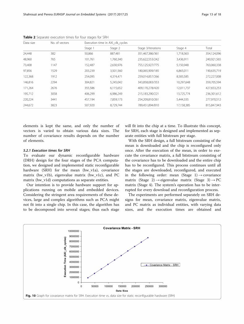
Fig. 10 Graph for covariance matrix for SRH. Execution time vs. data size for static reconfigurable hardware (SRH)
Shahrouzi and Perera EURASIP Journal on Embedded Systems (2017) 2017:25 Page 13 of 18

presented in Table 2. The execution time for each stageis measured 10 times, and the average is presented. Inthis case, the total execution times (last column ofTable 2) do not include the download and reconfigur-ation time between entities.As illustrated in Fig. 10, the execution time for the co-
variance matrix (for SRH) increases linearly with the sizeof the data. The mean and the PC matrix showed similarlinear behaviors. Similar to Fig. 12 for DRH design, theexecution time for eigenvalue matrix does not increaselinearly with the size of the original data set. It shouldbe noted that the input data size to the eigenvaluematrix is an mXm matrix, where m is the number ofelements of the vectors in the original data set. This mvalue is typically a constant for a certain data set; hencethe input data size to the eigenvalue matrix computationis the same regardless of the size of the original data set.
However, this execution time depends on and increaseslinearly with the number of iterations (similar to Fig. 13for DRH).
5.2.2 Execution times for DRHWith the DRH design, a full bitstream, which consists ofthe reconfigurable module (RM) of mean, is down-loaded, and the mean operation is performed. After theexecution of the mean, the partial bitstream for the RMof the covariance matrix is downloaded to the specificregion of the chip consisting of the mean module, andthat region is reconfigured to the covariance matrixoperation. Then the covariance matrix operation isperformed. This partial and dynamic reconfigurationprocess continues until all the stages of the PCA compu-tation are downloaded, reconfigured, and executed inthe following order: mean (Stage 1)→ covariance matrix
Table 3 Separate execution times for four stages for DRH
Datasize
No. ofvectors
Execution time in AXI_clk_cycles
Stage 1 S1→S2 reconfig. Stage 2 S2→S3 reconfig. Stage 3/iterations S3→S4 reconfig Stage 4 Total
24,448 382 50,879 68,103,418 887,481 68,121,324 351,467,386/361 68,112,480 1,718,389 558,461,357
48,960 765 101,761 68,097,812 1,760,340 68,108,008 235,622,553/242 68,109,251 3,436,924 445,236,649
73,408 1147 152,487 68,097,604 2,630,976 68,114,545 734,657,700/775 68,109,985 5,150,974 946,914,271
97,856 1529 203,239 68,098,307 3,501,560 68,120,760 180,065,909/185 68,108,534 6,865,011 394,963,320
122,368 1912 254,121 68,093,087 4,374,471 68,118,532 259,014,857/266 68,108,228 8,583,637 476,546,933
146,816 2294 304,821 68,097,653 5,245,029 68,117,134 343,858,083/353 68,112,569 10,297,674 564,032,963
171,264 2676 355,586 68,102,156 6,115,678 68,113,687 409,170,278/420 68,108,523 12,011,737 631,977,645
195,712 3058 406,299 68,102,063 6,986,275 68,119,069 215,183,290/221 68,110,364 13,725,761 440,633,121
220,224 3441 457,194 68,090,545 7,859,173 68,118,434 254,209,823/261 68,110,646 15,444,322 482,290,137
244,672 3823 508,843 68,074,050 8,730,693 68,095,324 789,451,907/810 68,088,858 17,159,321 1,020,108,996
Fig. 11 Graph for covariance matrix for DRH. Execution time vs. data size for dynamic reconfigurable hardware (DRH)
Shahrouzi and Perera EURASIP Journal on Embedded Systems (2017) 2017:25 Page 14 of 18

(Stage 2)→ eigenvalue matrix (Stage 3)→ PC matrix(Stage 4). In order to process varying data sizes or differ-ent data sets, the hardware is again reconfigured to thefirst PCA computation, i.e., mean operation, withoutdownloading the full bitstream or without interruptingthe system’s operation.Unlike SRH designs, for DRH designs, the execution
times are measured sequentially for consecutive stages ofthe PCA computations. The execution times for varyingdata sizes are measured 10 times, and the average is pre-sented in Table 3. The reconfiguration time overhead fromone stage to another are presented in columns 4, 6, and 8.The values in these three columns demonstrate that thereconfiguration time does not vary with the size of thedata set. Although there is a slight variation, it is less than1 ms. This is expected, since the reconfiguration time does
not depend on the number of data being processed but onthe size of the partial bitstream (i.e., the area of the RM).Similar to the SRH designs, as depicted in Fig. 11, the
execution time for the covariance matrix for DRH in-creases linearly with the size of the data set. The meanand the PC matrix showed similar linear behaviors. Fur-thermore, as shown in Fig. 12, the execution time foreigenvalue matrix for DRH does not increase linearlywith the size of the original data set, since the input datasize to the eigenvalue matrix computation is an mXmmatrix, and is the same regardless of the size of the ori-ginal data set (i.e., the number of vectors). However, asdemonstrated in Fig. 13, this execution time increaseslinearly with the number of iterations.From Table 3, it is evident that the eigenvalue matrix,
which is the largest and most complex design, takes the
Fig. 12 Graph for eigenvalue matrix for DRH (execution time vs. data size). Execution time vs. data size for dynamic reconfigurablehardware (DRH)
Fig. 13 Graph for eigenvalue matrix for DRH (execution time vs. number of iterations). Execution time vs. number of iterations for dynamicreconfigurable hardware (DRH)
Shahrouzi and Perera EURASIP Journal on Embedded Systems (2017) 2017:25 Page 15 of 18

longest time to process compared to other three stages,thus impacting the total execution time. As a result, thetotal execution time for the whole process increaseslinearly with the number of iterations.Figure 14 illustrates the percentage of reconfiguration
time (from the total execution time) vs. the number ofiterations for the DRH. For lower number of iterations, asignificant percentage of total time is spent on thereconfiguration. However, the percentage of recon-figuration time is amortized and decreases as the num-ber of iterations increases. This illustrates that the morecompute-intensive the operations are, the smaller theimpact of the reconfiguration time overhead is.
5.2.3 Speed-performance comparison: SRH and DRH vs.software on MicroBlazeAdditional software experiments are performed usingthe MicroBlaze soft processor on the same platform, inorder to evaluate the DRH as well as the SRH. Similar tothe DRH designs, the execution times for the softwaredesigns are also measured in a sequence: mean (Stage1)→ covariance matrix (Stage 2)→ eigenvalue (Stage3)→ PC (Stage 4). Execution times are obtained using
varying data sizes. However, only the largest data set ofsize 244,672 is used (presented in Table 4) for the per-formance comparison purposes for the two reconfigur-able hardware designs and the software designs.From Table 4, considering the total execution times,
the DRH is 53 times faster, while the SRH is 66 timesfaster than the equivalent software (Sw) running on theMicroBlaze. This difference is due to the time overheadincurred for reconfiguration for DRH. Although ourSRH is faster than our DRH, the space saving (asdemonstrated in Table 1) using the dynamic and partialreconfiguration is significant. It is important to considerthese speed-space tradeoffs, especially in mobile andembedded devices with their limited hardware footprint.Considering the execution times for individual modules,
SRH and DRH achieved similar speedups, and the speedupsvary from 60 to 79. It is evident that our current reconfigur-able hardware designs achieved superior speedups (79 timesfaster than software on MicroBlaze), compared to our pre-vious proof-of-concept designs (6 times faster than softwareon MicroBlaze) [32]. This significant improvement ofspeedups is due to several hardware optimization tech-niques we incorporated in our current designs including:
Fig. 14 Graph for number of iterations vs. percentage of reconfiguration time from total execution time. The percentage of reconfiguration timeis amortized and decreases as the number of iterations increases
Table 4 Performance Comparison: SRH and DRH vs. Software on MicroBlaze
Execution time in AXI_clk_cycles Speedup
SRH DRH Sw on MicroBlaze SRH vs. Sw DRH vs. Sw
Stage 1 507,920 508,843 30,564,884 60.18 60.07
Stage 2 8,729,744 8,730,693 686,064,039 78.59 78.58
Stage 3 789,451,894 789,451,907 51,909,640,837 65.75 65.75
Stage 4 17,158,385 17,159,321 1,246,451,248 72.64 72.64
Total 815,847,943 1,020,108,996 53,872,721,008 66.03 52.81
Shahrouzi and Perera EURASIP Journal on Embedded Systems (2017) 2017:25 Page 16 of 18

fully pipelined designs, designing computations to overlapwith memory access, and burst transfer and pre-fetchingtechniques to reduce the memory access latency.
6 ConclusionsIn this paper, we introduced reconfigurable hardwarearchitecture for PCA using partial reconfiguration method,which can be partially and dynamically reconfigured frommean→ covariance matrix→ eigenvalue matrix→ PCmatrix computations. This design showed a significantspace saving (about 71%), since the same area of the chip isbeing reused (by reconfiguring the hardware on chip fromone computation to another) for all the four stages of PCAcomputation, which is crucial for mobile and embeddeddevices with their limited hardware footprint.The extra hardware required for reconfiguration is
relatively low compared to the whole chip (about 1.28%)and remains constant regardless of the size of the recon-figuration module. Considering the reconfiguration timeoverhead, there is a difference between the theoreticalestimate and the experimental value. This is mainly be-cause we used a MicroBlaze processor as a configurationcontroller, which executes instruction sequentially. Wecould potentially get similar values as the theoreticalones, by using a FSM as the configuration controller anddownloading the configuration bitstream using “bit-par-allel” mode. Furthermore, we are investigating the exist-ing ICAP architectures and design techniques used in[16, 18, 25, 27] and planning to explore ways to designand incorporate similar techniques, to enhance the re-configuration process.Our current reconfigurable hardware designs executed
up to 79 times faster than the equivalent software runningon the embedded microprocessor. This is a significant im-provement from our proof-of-concept designs [32], whichexecuted up to 6 times faster than their software counterparts. From our proof-of-concept work [32], it was ob-served that a large amount of time (93–95%) was spent ondata transfer to/from the external memory, which used tobe a major performance bottleneck. This substantial im-provement of speedups is mainly due to several hardwareoptimization techniques we incorporated in our currentdesigns: burst transfer and pre-fetching techniques to re-duce the memory access latency, fully pipelined designs,designing computations to overlap with memory access.Our proposed hardware architectures are generic,
parameterized, and scalable. Hence, without changing theinternal hardware architecture, our hardware designs canbe used to process different data sets with varying numberof vectors and with varying number of dimensions; usedfor any embedded applications that employ the PCAcomputation; executed on different development plat-forms, including platforms with recent FPGAs such asVirtex-7 chips.
Power consumption is another major issue in mobileand embedded devices. As demonstrated in [30],although reconfigurable hardware typically consumesless power than microprocessor-based software-onlydesigns, we are planning and designing experiments toevaluate the power consumption in reconfigurablehardware designs for data mining applications.The results shown in our experiments are encouraging
and demonstrate great potential in implementing datamining applications such as PCA computation using re-configurable platform. Complex applications can indeedbe implemented in reconfigurable hardware for mobileand embedded applications.
Authors’ contributionsDGP has been conducting this research and performed the proof-of-conceptwork. SNS is DGP’s student. DGP and SNS have designed the SRH and DRH aswell as the software for the PCA computation. Under the guidance of DGP, SNShas implemented the reconfigurable hardware for the PCA computations andperformed the experiments. DGP wrote the paper. Both authors read andapproved the final manuscript.
Authors’ informationS. Navid Shahrouzi received his M.Sc. and B.Sc. degrees in Electronics and ElectricalEngineering from University of Guilan (Iran) in 2007 and K.N.Toosi University ofTechnology (Iran) in 2004, respectively. Navid is pursuing his Ph.D. and working asa research assistant in the Department of Electrical and Computer Engineering,University of Colorado under the guidance of Dr. Darshika G. Perera. His researchinterests are digital systems and hardware optimization.Darshika G. Perera is an Assistant Professor in the Department of Electricaland Computer Engineering, University of Colorado, USA, and also anAdjunct Assistant Professor in the Department of Electrical and ComputerEngineering, University of Victoria, Canada. She received her Ph.D. degree inElectrical and Computer Engineering from University of Victoria (Canada),and M.Sc. and B.Sc. degrees in Electrical Engineering from Royal Institute ofTechnology (Sweden) and University of Peradeniya (Sri Lanka), respectively.Prior to joining University of Colorado, Darshika worked as the SeniorEngineer and Group Leader of Embedded Systems at CMC Microsystems,Canada. Her research interests are reconfigurable computing, mobile andembedded systems, data mining, and digital systems. Darshika received abest paper award at the IEEE 3PGCIC conference in 2011. She serves onorganizing and program committees for several IEEE/ACM conferences andworkshops and as a reviewer for several IEEE, Springer, and Elsevier journals.She is a member of the IEEE, the IEEE Computer Society, and the IEEEWomen in Engineering.
Competing interestsThe authors declare that they have no competing interests.
Received: 14 July 2016 Accepted: 8 February 2017
References1. JFD Addison, S Wermter, GZ Arevian, A comparison of feature extraction
and selection techniques, in Proc. of Int. Conf. on Artificial Neural Networks(ICANN), 2003, pp. 212–215
2. Agilent Technologies, Inc, Principal component analysis, 2005, Santa Clara,CA, USA http://sorana.academicdirect.ro/pages/collagen/amino_acids/materials/PCA_1.pdf. Accessed in June 2016
3. E Alpaydin, C Kaynak, Optical recognition of handwritten digits data set.Available in UCI Machine Learning Repository, July 1998
4. P Berkhin, Survey of clustering data mining techniques. Technical Report,Accrue Software, 2002
5. K Compton, S Hauck, Reconfigurable computing: a survey of systems andsoftware. ACM Computing Surveys (CSUR) 34(2), 171–210 (2002)
6. Data mining: what is data mining? http://www.anderson.ucla.edu/faculty/jason.frand/teacher/technologies/palace/datamining.htm. Accessed in June 2016
Shahrouzi and Perera EURASIP Journal on Embedded Systems (2017) 2017:25 Page 17 of 18

7. J DeCoster, Overview of factor analysis, 1998. http://www.stat-help.com/notes.html. Accessed in June 2016
8. CHQ Ding, X He, Principal component analysis and effective k-meansclustering, in Proc. of SDM, 2004
9. D Dye, Partial reconfiguration of Xilinx FPGAs using ISE design suite, WP374(v1.1), 2011
10. V Eck, P Kalra, R LeBlanc, J McManus, In-circuit partial reconfiguration ofrocketIO attributes XAPP662 (v2.4), 2004
11. K Fukunaga, Introduction to statistical pattern recognition, 2nd edn.(Academic, New York, 1990)
12. P Garcia P, K Compton, M Schulte , E Blem, and W Fu. An overview ofreconfigurable hardware in embedded systems. EURASIP Journal onEmbedded Systems, (2006), 1–19
13. A Gnanabadkaran, K Duraiswamy, An efficient approach to cluster highdimensional spatial data using K-mediods algorithm. European Journal ofScientific Research 49(4), 617–624 (2011)
14. GH Golub, CF van Loan, Matrix computations, 3rd edn. (John HopkinsUniversity Press, Baltimore, 1996)
15. DJ Hand, H Mannila, P Smyth, Principles of data mining (The MIT Press,Cambridge, 2001)
16. SG Hansen, D Koch, J Torresen, High speed partial run-time reconfigurationusing enhanced ICAP hard macro, in Proc. of IEEE International Symposiumon Parallel and Distributed Processing Workshops and Phd Forum (IPDPSW),2011, pp. 174–180
17. S Hauck, and A Dehon Reconfigurable computing: the theory and practiceof FPGA-based computing (Morgan Kaufmann Publishers Inc. San Francisco,CA, USA., 2008)
18. M Hübner, D Göhringer, J Noguera, J Becker, Fast dynamic and partialreconfiguration data path with low hardware overhead on Xilinx FPGAs, inProc. of Reconfigurable Architectures Workshop (RAW’10), 2010
19. J Hussein, R Patel, MultiBoot with Virtex-5 FPGAs and Platform Flash XL,XAPP1100 (v1.0), 2008
20. A Hyvarinen, A survey on independent component analysis. NeuralComputing Survey 2, 94–128 (1999)
21. JE Jackson, A user’s guide to principal components (John Wiley & Sons, Inc.Publications, Wiley-Interscience, Hoboken, New Jersey, USA, 2003)
22. AK Jain, MN Murty, PJ Flynn, Data clustering: a review. ACM ComputingSurveys 31(3), 264–323 (1999)
23. IT Jolliffe, Principal component analysis (Springer, New York, 2002)24. HP Kriegel, P Kröger, A Zimek, Clustering high-dimensional data: a survey on
subspace clustering, pattern-based clustering, and correlation clustering.ACM Transactions on Knowledge Discovery from Data, (TKDD), New York,NY, USA, 3(1), 1–58 (2009)
25. V Lai, O Diessel, ICAP-I: a reusable interface for the internal reconfigurationof Xilinx FPGA, in Proc. of International Conference on Field-ProgrammableTechnology (FPT), 2009, pp. 357–360
26. D Lim, M Peattie, Two flows for partial reconfiguration: module based andsmall bit manipulation, XAPP290, 2002
27. M Liu, W Kuehn, Z Lu, A Jantsch, Run-time partial reconfiguration speedinvestigation and architectural design space exploration, in Proc. of IEEEInternational Workshop on Field Programmable Logic and Applications (FPL), 2009,pp. 498–502
28. DC Manning, P Raghvan, and H Schutze, Introduction to informationretrieval. Cambridge University Press (2008)
29. PJ Olver, Orthogonal bases and the QR algorithm. University ofMinnesota, (2008)
30. DG Perera, KF Li, Analysis of single-chip hardware support for mobile andembedded applications, in Proc. of IEEE Pacific Rim Int. Conf. onCommunication, Computers, and Signal Processing, 2013, pp. 369–376
31. DG Perera, KF Li, Embedded hardware solution for principal componentanalysis, in Proc. of IEEE Pacific Rim Int. Conf. on Communication, Computersand Signal Processing (PacRim’11), 2011, pp. 730–735
32. DG Perera, and KF Li, FPGA-based reconfigurable hardware for computeintensive data mining applications, In Proc. of 6th IEEE Int. Conf. on P2P,Parallel, Grid, Cloud and Internet Computing (3PGCIC’11), 2011,pp.100-108. (Best Paper Award)
33. K Reddy, T Herron, Computing the eigen decomposition of a symmetricmatrix in fixed-point arithmetic, in Proc. of 10th Annual Symp. on MultimediaCommunication and Signal Processing, 2001
34. G Salton, MJ McGill, Introduction to modern information retrieval(McGraw-Hill, New York, 1983)
35. P Sedcole, B Blodget, T Becker, J Anderson, P Lysaght, Modular dynamicreconfiguration in Virtex FPGAs. IEE Computers and Digital Techniques153(3), 157–164 (2006)
36. A Sharma, KK Paliwal, Fast principal component analysis using fixed-pointalgorithm. Pattern Recognition Letters 28(10), 1151–1155 (2007)
37. J Shlens, A tutorial on principal component analysis. Institute on NonlinearScience, UCSD, Salk Insitute for Biological Studies, La Jolla, CA, USA. (2005).http://www.cs.cmu.edu/~elaw/papers/pca.pdf. Accessed in June 2016
38. LI Smith, A tutorial on principal component analysis. Cornell University, 200239. M Thangavelu, R Raich, On linear dimension reduction for multiclass
classification of Gaussian mixtures, in Proc. of IEEE Int. Conf. on MachineLearning and Signal Processing, 2009, pp. 1–6
40. TJ Todman, GA Constantinides, SJE Wilton, O Mencer, W Luk, PYK Cheung,Reconfigurable computing: architectures and design methods. IEEComputer and Digital Techniques 152(2), 193–207 (2005)
41. LN Trefethen, and D Bau, Numerical linear algebra. (SIAM Bookstore,Philadelphia, PA, USA, 1997)
42. P Valarmathie, MV Srinath, K Dinakaran, An increased performance of clusteringhigh dimensional data through dimensionality reduction technique.Theoretical and Applied Information Technology 5(6), 731–733 (2005)
43. Xilinx, Inc., LogiCORE IP AXI HWICAP, DS817 (v2.03.a) (2012). http://www.xilinx.com/support/documentation/ip_documentation/axi_hwicap/v2_03_a/ds817_axi_hwicap.pdf. Accessed in June 2016
44. Xilinx, Inc., LogiCORE IP AXI System ACE Interface Controller, DS789 (v1.01.a)(2012). http://www.xilinx.com/support/documentation/ip_documentation/ds789_axi_sysace.pdf. Accessed in June 2016
45. Xilinx, Inc., LogiCORE IP Block Memory Generator, PG058 (v7.3) (2012).http://www.xilinx.com/support/documentation/ip_documentation/blk_mem_gen/v7_3/pg058-blk-mem-gen.pdf. Accessed in June 2016
46. Xilinx, Inc., LogiCORE IP AXI Interconnect, DS768 (v1.06.a) (2012).http://www.xilinx.com/support/documentation/ip_documentation/axi_interconnect/v1_06_a/ds768_axi_interconnect.pdf. Accessed in June 2016
47. Xilinx, Inc., LogiCORE IP AXI Master Burst (axi_master_burst), DS844 (v1.00.a)(2011). http://www.xilinx.com/support/documentation/ip_documentation/axi_master_burst/v1_00_a/ds844_axi_master_burst.pdf. Accessed in June 2016
48. Xilinx, Inc., LogiCORE IP AXI SystemACE Interface Controller, DS789 (v1.01.a)(2011). http://www.xilinx.com/support/documentation/ip_documentation/ds789_axi_sysace.pdf. Accessed in June 2016
49. Xilinx, Inc., LogiCORE IP AXI Timer, DS764 (v1.03.a) (2012). http://www.xilinx.com/support/documentation/ip_documentation/axi_timer/v1_03_a/axi_timer_ds764.pdf. Accessed in June 2016
50. Xilinx, Inc., LogiCORE IP Floating-Point Operator, DS335 (v5.0) (2011).http://www.xilinx.com/support/documentation/ip_documentation/floating_point_ds335.pdf. Accessed in June 2016
51. Xilinx, Inc., ML605 Hardware User Guide, UG534 (v1.5) (2011). www.xilinx.com/support/documentation/boards_and_kits/ug534.pdf, Accessed in June 2016
52. Xilinx, Inc., Partial Reconfiguration User Guide UG702 (v12.3) (2010).http://www.xilinx.com/support/documentation/sw_manuals/xilinx12_3/ug702.pdf. Accessed in June 2016
53. Xilinx, Inc., PlanAhead User Guide, UG632 (v 11.4) (2009). http://www.xilinx.com/support/documentation/sw_manuals/xilinx11/PlanAhead_UserGuide.pdf.Accessed in June 2016
54. Xilinx, Inc., Virtex 6 FPGA Memory Interface Solutions, DS186 (v1.03.a) (2012).http://www.xilinx.com/support/documentation/ip_documentation/mig/v3_92/ds186.pdf. Accessed in June 2016
55. Xilinx, Inc., Virtex-6 FPGA Configuration User Guide UG360 (v3.2) (2010).http://www.xilinx.com/support/documentation/user_guides/ug360.pdf.Accessed in June 2016
56. JT Yao, Sensitivity analysis for data mining, in Proc. of 22nd Int. Conf. of FuzzyInformation Processing Society, 2003, pp. 272–277
57. KY Yeung, and WL Ruzzo, Principal component analysis for clustering geneexpression data. Bioinformatics. 9, 763-774, (2001)
Shahrouzi and Perera EURASIP Journal on Embedded Systems (2017) 2017:25 Page 18 of 18