dye-sensitized tio nanotube solar cells with markedly ...nanofm.mse.gatech.edu/papers/wang j and lin...
TRANSCRIPT
pubs.acs.org/cmPublished on Web 12/08/2009r 2009 American Chemical Society
Chem. Mater. 2010, 22, 579–584 579DOI:10.1021/cm903164k
Dye-Sensitized TiO2 Nanotube Solar Cells with Markedly Enhanced
Performance via Rational Surface Engineering
Jun Wang and Zhiqun Lin*
Department of Materials Science and Engineering, Iowa State University, Ames, Iowa 50011
Received October 14, 2009. Revised Manuscript Received November 14, 2009
Highly ordered anodic TiO2 nanotube arrays fabricated by electrochemical anodization weresensitized with ruthenium dye N-719 to yield dye-sensitized TiO2 nanotube solar cells. Rationalsurface treatments on photoanode TiO2 nanotubes markedly improved the device performance.With TiCl4 treatment, in conjunction with oxygen plasma exposure under optimized conditions,dye-sensitized TiO2 nanotube solar cells produced using 14-μm-thick TiO2 nanotube arrays inbackside illumination mode subjected to simulated AM 1.5G irradiation of 100mW/cm2 exhibited apronounced power conversion efficiency (PCE) of 7.37%.
As one of the major renewable energy sources, solarenergy has the potential to become an essential compo-nent of future global energy production. Dye-sensitizedsolar cells (DSSCs),1 represent one of the most promisingof several alternative, cost-effective concepts for solar-to-electric energy conversion that has been offered to chal-lenge conventional silicon solar cells over the past decade.The configuration of a DSSC consists of a sintered, wide-bandgap semiconductor TiO2 nanoparticle network film,a ruthenium-based dye (i.e., sensitizer), and an electro-lyte. Upon the absorption of photons, the dye generatesexcitons (i.e., electron-hole pairs). Subsequently, theelectrons inject into the TiO2 photoanode to generatephotocurrent; scavenged by a redox couple, holes trans-port to the cathode. The performance of a DSSC can beimproved by optimizing the semiconductor TiO2 nano-particle film, sensitizer, and electrolyte. An overall powerconversion efficiency (PCE) of>10% for aDSSC, whichis dictated by its light harvest efficiency, the quantumyield for charge injection, and the charge collectionefficiency at the electrodes,2 has been demonstrated.However, much research remains to be done to improvethe efficiency and remove the practical problems relatedto DSSCs. For example, typically, a 10-μm-thick meso-porous TiO2 (anatase nanocrystals) film with a porosityof 50% is employed as an electron-accepting species in aDSSC. The film is prepared by dispersing 15-30 nmcolloidal TiO2 particles on a conductive glass supportconsisting of a network of randomly dispersed nanocrys-tals.3 While versatile and robust, these sintered three-dimensional TiO2 nanoparticle films lead to enhanced
scattering of free electrons and electron trapping at theinterfaces, thereby reducing electron mobility and exhi-biting slow electron transport. The electron and holetransport across several ill-defined, heterogeneous inter-faces in TiO2 nanoparticle films is very complex.4
In this context, highly ordered, vertically oriented TiO2
nanotube arrays of different aspect ratios and surfacequalities have recently been fabricated as alternativenanoscale architectures to substitute the sintered TiO2
nanoparticle films in DSSCs. They are produced bypotentiostatic anodization of titanium (Ti) foil5,6 or Tithin films that have been sputtered using radio-frequency(RF) sputter deposition on a variety of substrates withfluorine-containing electrolytes (e.g., fluorine-doped tinoxide (FTO)-coated glass).7 The nanotubular morphol-ogy of these arrays offers a large internal surface areawithno concomitant decrease in geometric and structuralorder.5 The vertical orientation of the crystalline nano-tube arrays after annealing makes them excellent electronpercolation pathways for efficient, vectorial charge trans-port along the nanotube axis.5 A PCE of 2.9% wasachieved using a 360-nm-thick transparent TiO2 nano-tube membrane to assemble DSSCs in a front side illu-mination mode,8 and the performance was furtherimproved to 6.9% with the capability of growing thickerTiO2 nanotube arrays on transparent substrates.9 A PCEof 6.89% was also obtained using 20-μm-thick TiO2
nanotube arrays that were grown on Ti foil in a backside
*Author to whom correspondence should be addressed. E-mail: [email protected].(1) Gratzel, M. Nature 2001, 414, 338.(2) O’Regan, B.; Gratzel, M. Nature 1991, 353, 737.(3) Nazeeruddin, M. K.; Kay, A.; Rodicio, I.; Humpbry-Baker, R.;
Miiller, E.; Liska, P.; Vlachopoulos, N.; Gratzel, M. J. Am. Chem.Soc. 1993, 115, 6382.
(4) Martinson, A. B. F.; Hamann, T. W.; Pellin, M. J.; Hupp, J. T.Chem.;Eur. J. 2008, 14, 4458.
(5) Grimes, C. A. J. Mater. Chem. 2007, 17, 1451.(6) Macak, J. M.; Tsuchiya, H.; Taveira, L.; Aldabergerova, S.;
Schmuki, P. Angew. Chem., Int. Ed. 2005, 44, 7463.(7) Mor, G. K.; Varghese, O. K.; Paulose, M.; Grimes, C. A. Adv.
Funct. Mater. 2005, 15, 1291.(8) Mor, G. K.; Varghese, O. K.; Paulose, M.; Ong, K. G.; Grimes, C.
A. Thin Solid Films 2006, 496, 7.(9) Varghese, O. K.; Paulose, M.; Grimes, C. A. Nat. Nanotechnol.
2009, 4, 592.
580 Chem. Mater., Vol. 22, No. 2, 2010 Wang and Lin
illumination mode.10 Recently, an improved PCE inquantum-dot-sensitized solar cells was achieved by facil-itating the charge transport through TiO2 nanotubearchitecture (PCE e 1%) rather than sintered TiO2
nanoparticle film.11 Comparing solar cells produced fromTiO2 nanotube arrays with that from sintered TiO2
nanoparticle films, enhanced charge collection efficiencyand enhanced light scattering in TiO2 nanotube-basedDSSC was observed.12 The use of TiO2 nanotubes re-duced carrier scattering loss and nonradiative recombi-nation by eliminating unnecessary lateral transport (i.e.,hopping between TiO2 nanoparticles) and its resultingrecombination loss. It is noteworthy that the dye absorp-tion on TiO2 nanotubes was found to be similar to that onTiO2 nanoparticle films of identical film thickness, ac-cording to the dye loading measurement.12
Surface treatment on TiO2 photoanodes not only in-creased the loading of sensitizers on the TiO2 surface butalso improved the electronic interaction between thesensitizer (i.e., dye) and the TiO2 surface, thereby yieldingimproved device performance.13,14 For example, an in-creased PCE of the DSSC was obtained by exposing theTiO2 nanoparticle film to O2 plasma.13 The O2 plasmatreatment promoted the hydrophilicity on the TiO2 sur-face, leading to the increased dye adsorption. It has beendemonstrated that by exposing ZnO nanowires to O2
plasma, the grafting density of CdSe quantum dots onthe ZnO nanowire surface increased dramatically, result-ing in an improvedPCE.15Notably, the treatment of TiO2
nanotubes with O2 plasma has yet been studied. On theother hand, immersing photoanodes (e.g., TiO2 or ZnO)in titanium tetrachloride (TiCl4) solution led to the for-mation of a very thin TiO2 blocking layer. As a result, theamount of dye adsorption was increased and the chargetransfer from dye molecules to photoanodes was facili-tated, and, ultimately, an enhanced PCE was readilyobtained.14,16
In this article, we report dye-sensitized TiO2 nanotubesolar cells with enhanced performance based on highlyordered, vertically oriented TiO2 nanotube arrays afterrational surface engineering, i.e., the TiCl4 processingfollowed by O2 plasma exposure. The TiO2 nanotubearrays were fabricated by electrochemical anodization;subsequently, they were impregnated with ruthenium dyeN-719 that was used as sensitizer and chemically an-chored to the surface of TiO2 nanotubes via the reac-tion of carboxylate moieties on N-719 surface with
complementary hydroxyl groups on the TiO2 surface.The PCE of solar cells produced using 14-μm-thickTiO2 nanotube arrays under simulated AM1.5G irradia-tion of 100mW/cm2 in backside illuminationmode raisedfrom 4.34% to 7.37% after immersion in the TiCl4solution followed by exposure to O2 plasma. The TiCl4andO2 plasma exposure processes led to increased photo-generated current and fill factor, ultimately, a higherPCE. To the best of our knowledge, the PCE of 7.37%is highest performance among dye-sensitized TiO2 nano-tube solar cells reported, thereby offering an avenue indeveloping high-efficiency solar cells for renewable en-ergy production.
Experimental Section
Fabrication of TiO2 Nanotube Arrays. High-purity Ti foil
(250 μm thick, 99.7% purity, Sigma-Aldrich) was cut into pieces,
each 1 in. � 0.5 in. in size, and degreased by ultrasonication for
30 min in a mixture of acetone, methanol, and methylene
chloride, followed by a thorough rinse with deionized (DI)
water and blow-dried with N2. Ethylene glycol (Fisher Scien-
tific) was used as the electrolyte in which a small amount of
ammonium fluoride (Sigma-Aldrich) was added. Electroche-
mical anodization of titanium was performed in a two-electrode
cell at room temperature using a EC570-90 power source
(Thermo Electron Corporation) at 60 V. A platinum foil was
used as the counter electrode. After anodization, the Ti foil with
TiO2 nanotubes grown on one side of its surface was extensively
washed with DI water and dried with N2 (the backside of the Ti
foil was protected with a layer of insulate resin to prevent
oxidation during the anodization process).
Surface Treatment. Prior to dye adsorption, anatase TiO2
nanotubes were processed with TiCl4 by immersing them in
50 mL of 0.2 M TiCl4 aqueous solution in a beaker sealed with
parafilm and kept in a 60 �C oil bath for 1 h, followed by rinsing
with ethanol and annealed at 500 �C in air for 30min. The TiCl4-
treated TiO2 nanotubes were further exposed to O2 plasma at
30 W of power for different times.
TiO2 Nanotube Solar Cell Fabrication. The surface-treated
TiO2 nanotube arrays were then immediately soaked in a
0.2 mM dye/ethanol solution for 24 h to allow complete dye
adsorption. The dye used in the study was cis-diisothiocyanato-
bis(2,20-bipyridyl-4,40-dicarboxylato) ruthenium(II) bis(tetra-
butylammonium) (N-719, Solaronix). A semitransparent plati-
num (Pt)-coated ITO glass was used as the counter electrode,
prepared by placing a drop of 0.5 mM chloroplatinic acid
(H2PtCl6)/isopropanol solution on ITO glass and subsequently
fired at 380 �C for 20 min. The dye-sensitized TiO2 nanotube
arrays were sandwiched between the Ti foil (anode) and the Pt-
coated ITO glass (cathode) by applying a 25-μm-thick hot-melt
sealing foil as the spacer (SX1170-25, Solaronix). An ionic liquid
electrolyte containing 0.60 M BMIM-I, 0.03 M I2, 0.50 M TBP,
and 0.10MGTC in acetonitrile/valeronitrile 85/15 (v/v) (No. ES-
0004, purchased from io.li.tec, Germany) was injected between
two electrodes driven by capillary force through holes on the
hot-melt sealing foil. The ionic liquid possesses high thermal
stability, negligible vapor pressure, and low toxicity. The back-
side of the Ti foil was then scratched using sandpaper to remove
the thin oxide layer, thereby exposing the underlying titanium
that serves as the electrode.
Characterization. Scanning electron microscopy (SEM) ima-
ging was performed with a JEOL Model LV 5800 microscope.
(10) Shankar, K.; Mor, G. K.; Prakasam, H. E.; Yoriya, S.; Paulose,M.; Varghese, O. K.; Grimes, C. A. Nanotechnology 2007, 18,065707.
(11) Kongkanand, A.; Tvrdy, K.; Takechi, K.; Kuno,M.; Kamat, P. V.J. Am. Chem. Soc. 2008, 130, 4007.
(12) Zhu, K.; Neale, N. R.;Miedaner, A.; Frank, A. J.Nano Lett. 2007,7, 69.
(13) Boercker, J. E.; Enache-Pommer, E.; Aydil, E. S. Nanotechnology2008, 19, 095604.
(14) Mor,G.K.; Shankar,K.; Paulose,M.; Varghese, O.K.;Grimes, C.A. Nano Lett. 2006, 6, 215.
(15) Leschkies, K. S.; Divakar, R.; Basu, J.; Enache-Pommer, E.;Boercker, J. E.; Carter, C. B.; Kortshagen, U. R.; Norris, D. J.;Aydil, E. S. Nano Lett. 2007, 7, 1793.
(16) Liu, B.; Aydil, E. S. J. Am. Chem. Soc. 2009, 131, 3985.
Article Chem. Mater., Vol. 22, No. 2, 2010 581
Raman spectroscopy measurements were performed using a
Renishaw inVia Raman microscope excited with a 488-nm
Arþ laser at 5 mW with an acquisition time of 10 s. The
current-voltage (I-V) curves were measured using a Keithley
Model 2400 multisource meter. A solar simulator (SoLux Solar
Simulator) was used to simulate sunlight, with an illumination
intensity of 100 mW/cm2 (calibrated with Daystar Meter). The
photoactive area for all solar cells was 0.125 cm2.
Results and Discussion
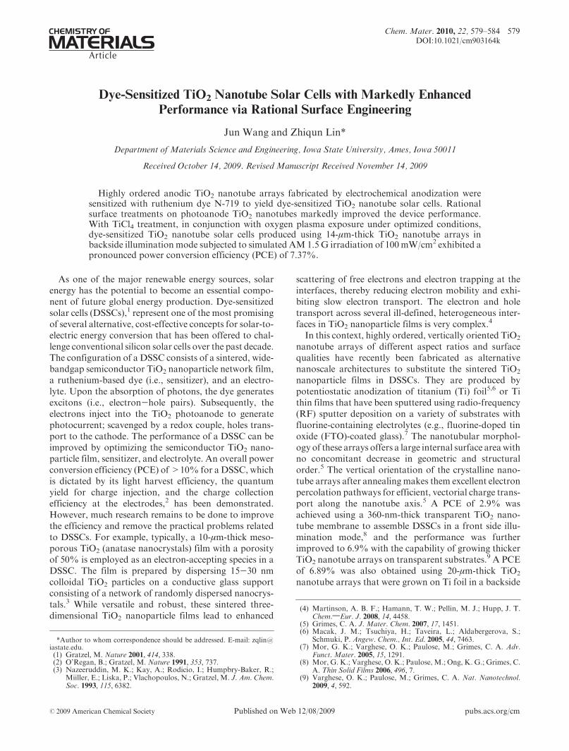
Highly ordered TiO2 nanotube arrays were fabricatedaccording to our previously reported procedure.17-19 TheSEM images of as-prepared TiO2 nanotube arrays areshown in Figures 1a-c. The nanotubes had an averageinner diameter of 90 nm and an interpore distance of120 nm (see Figures 1a and 1c). Themembrane thickness canbe readily controlled by the anodization time; the crosssection of a 14-μm-thick TiO2 membrane obtained after2 h of anodization is shown in Figure 1b. We note thatTiO2 nanotube arrays with thicknesses of 22 and 29 μmwere obtained after 3 h and 4 h of anodization, respec-tively. The as-prepared TiO2 nanotubes were amorphous.To take advantage of nanotubular structures for use insolar cells, they should be converted to crystalline forms,i.e., anatase or rutile phase. The crystalline phase, inducedby thermal annealing at 500 �C in air for 3 h,19 was con-firmed by Raman spectroscopy. A broad spectrum wasseen on amorphous TiO2 nanotubes. By contrast, specificRaman peaks at 145, 196, 399, 516, and 640 cm-1 were
observed from annealed TiO2 nanotube arrays, signifyingthe formation of anatase TiO2 (see Figure 1d).
19 The TiO2
nanotubular structures were maintained after high-tem-perature annealing.19
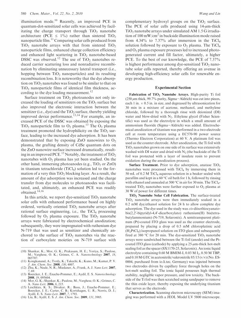
Anatase TiO2 nanotube arrays were then utilized asphotoanodes to assemble dye-sensitized nanostructuredsolar cells (see Scheme 1). Prior to dye adsorption, thenanotubes were processed with TiCl4 using 0.2 M TiCl4aqueous solution.14,16 Subsequently, the TiCl4-treatedTiO2 nanotube arrays were exposed to O2 plasma fordifferent time. The N-719 dye-sensitized TiO2 nanotubesolar cells were assembled and the performance wasmeasured (see the Experimental Section).Figure 2 shows the effects of TiCl4 treatment on the
I-V characteristics of dye-sensitized TiO2 nanotubesolar cells. The thickness of TiO2 nanotube arrays was14 μm. For solar cell without subjecting to TiCl4 process-ing, the measurement yielded an open circuit voltage(VOC) of 0.70 V, a short circuit current density (JSC) of12.16 mA/cm2, and a fill factor (FF) of 0.51; thus, thepower conversion efficiency (PCE), which is defined as
Figure 1. Structural characterization of highly ordered TiO2 nanotube arrays: (a) SEM topology, scale bar = 1 μm; (b) SEM cross-sectional view, scalebar=10μm; (c) SEMcross-sectional view, scale bar=1μm;and (d)Raman spectra of amorphous (black curve) and crystalline (red curve) TiO2 nanotubearrays, where the Raman peaks at 145, 196, 399, 516, and 640 cm-1 suggest the formation of anatase TiO2.
Scheme 1. Schematic Illustration of the Configuration of a Dye-Sensitized TiO2 Nanotube Solar Cell
(17) Wang, J.; Lin, Z. Chem. Mater. 2008, 20, 1257.(18) Wang, J.; Lin, Z. Q. J. Phys. Chem. C 2009, 113, 4026.(19) Wang, J.; Zhao, L.; Lin, V. S. Y.; Lin, Z. Q. J. Mater. Chem. 2009,
19, 3682.
582 Chem. Mater., Vol. 22, No. 2, 2010 Wang and Lin
PCE ¼ ISCVOCFFPinc
is 4.34% (see curve b in Figure 2). Incontrast, when TiCl4-treated TiO2 nanotube arrays wereused, the performance sharply increased, yielding valuesof VOC = 0.75 V, JSC = 12.48 mA/cm2, FF = 0.68, andPCE=6.36% (see curve c inFigure 2), which represents a47% increase in PCE, when compared to its non-TiCl4-treated counterpart (see curve b in Figure 2). The perfor-mance improvement can be rationalized as follows. Uponhigh-temperature annealing, there existed structural de-fects and cracks on the nanotubes, aswell as on the barrierlayer (i.e., structural disorders),17,20 which made it possi-ble for the electrolyte to have direct contact with the Tielectrode on the bottom, leading to decreased shuntresistance and higher chance for charge recombination.By contrast, with TiCl4 treatment, a thin blocking layer ofTiO2 can be formed on the uncovered region of Ti foil,16
thus reducing or eliminating the structural disorders. As aconsequence, the shunt resistance increased and seriesresistance decreased; this improved the FF value, and,ultimately, a higher PCE was obtained.16 With TiCl4treatment, the increased electron transport through aTiO2 nanotube wall to the bottom Ti electrode by de-creasing the surface charge recombination, as well as theincreased dye adsorption by facilitating improved bond-ing between TiO2 and dye molecules, may also contributeto the enhanced performance.14,16
O2 plasma treatment has been demonstrated as aneffective approach to saturate the metal oxide surfacewith hydroxyl group,21 which increases the hydrophilicityat the metal oxide surface.15 In this regard, to furtherimprove the performance of dye-sensitized nanostruc-tured solar cells, O2 plasma exposure was performed onthe TiCl4-treated TiO2 nanotubes prior to infiltration ofdye N-719. Specifically, the aforementioned TiCl4-trea-ted, 14-μm-thick TiO2 nanotube arrays were placed in anO2 plasma cleaner (Harrick Plasma Model PDC-001;
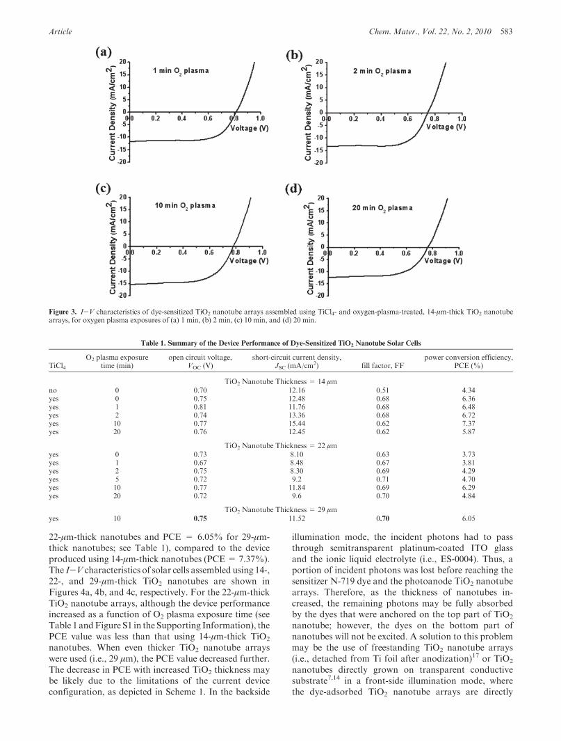
a PlasmaFlo gas meter was used to control the O2 flowin the reaction chamber). The plasma condition wasoptimized by tuning the O2 flow and vacuum until thebrightest fluorescence was observed, i.e., with the O2 flowof 1 SCFH and a vacuum of 500 mTorr. After plasmaexposure for different periods of time, TiO2 nanotubeswere immersed in the 0.2 mMN-719/ethanol solution for24 h. All other steps for the construction of solar cells andthe performance measurements were maintained thesame. The I-V curves of resulting solar cells are shownin Figure 3. In comparison to curve c in Figure 2, in whichTiO2 nanotubes were not subjected to O2 plasma (PCE=6.36%), the PCE increased to 6.48% after 1 min O2
plasma treatment. With longer time exposure to O2
plasma, the PCE increased; the highest PCE value of7.37% was achieved from the 10-min O2 plasma-treatedsample (see Table 1 for complete device characterization).The enhancement in PCE can be attributed to a largeincrease in the photocurrent density (JSC), while thephotovoltage (VOC) did not change much and the fillfactor (FF) slightly decreased. Upon O2 plasma treat-ment, the hydroxyl group on the TiO2 surface increasedand eventually saturated; this promoted the adsorption ofthe N-719 dye by forming interfacial bonding betweenN-719 and the TiO2 via the coupling reaction of terminalcarboxylic acid groups on N-791 with complementaryhydroxyl groups on the TiO2 surface, thereby substan-tially regulating the interfacial charge transfer fromN-719 dye to TiO2 and, therefore, the ultimate photo-physical properties at the nanoscale.Note that, upon lengthy O2 plasma exposure (e.g.,
20 min; see Figure 3d and Table 1), the device per-formance decreased, exhibiting a largely reduced JSCvalue, compared to the sample after 10 min of O2
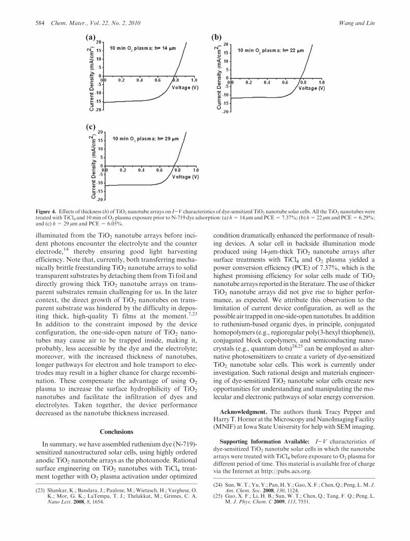
plasma exposure (see Figure 3c and Table 1). The exactreason for this observation is not clear. It may be becausethe TiO2 surface became less hydrophilic after a lon-ger-time plasma exposure than that under the opti-mized condition.22 Consequently, the dye loading wasreduced, which, in turn, the decreased device perfor-mance. Similar trends were seen in solar cells assembledusing 22- and 29-μm-hick TiO2 nanotube arrays, that is,the PCE increased with time when nanotubes were sub-jected to O2 plasma for<10min; otherwise, the PCE wasreduced (see Table 1 and Figure S1 in the SupportingInformation).We note that increasing the thickness of TiO2 nanotube
arrays may be a good strategy to improve the perfor-mance of solar cells by allowing more dye molecules to beadsorbed on the TiO2 nanotube surface and, thus, ahigher light harvesting efficiency. To this end, thickerTiO2 nanotube arrays 22 and 29 μm in thickness wereprepared and used to fabricate solar cells; they wereprocessed with TiCl4 and oxygen plasma. Quite intrigu-ingly, the use of thicker TiO2 nanotube arrays yieldedprogressively decreased performance (PCE = 6.29% for
Figure 2. Current-voltage (I-V) characteristics of dye-sensitized TiO2
nanotube solar cells. The thickness of TiO2 nanotube membrane was14 μm. (a) the device in the dark; anatase TiO2 nanotube arrays were nottreated with TiCl4 (the devices with and without TiCl4 treatment wereindistinguishable in the dark); (b) the device made of anatase TiO2
nanotube arrays without TiCl4 treatment under AM 1.5 G illumination,yielding a fill factor (FF) of 51% and power conversion efficiency (PCE)of 4.34%; and (c) the device made of the TiCl4-treated TiO2 nanotubearrays under AM 1.5 G illumination, yielding values of FF = 68% andPCE= 6.36%.
(20) Zhu,K.; Vinzant, T. B.; Neale, N.R.; Frank,A. J.NanoLett. 2007,7, 3739.
(21) Tsoi, S.; Fok, E.; Sit, J. C.; Veinot, J. G. C. Langmuir 2004, 20,10771.
(22) Lu, D.; Wu, Y.; Guo, J. H.; Lu, G.; Wang, Y.; Shen, J. C. Mater.Sci. Eng. B 2003, 97, 141.
Article Chem. Mater., Vol. 22, No. 2, 2010 583
22-μm-thick nanotubes and PCE = 6.05% for 29-μm-thick nanotubes; see Table 1), compared to the deviceproduced using 14-μm-thick nanotubes (PCE= 7.37%).The I-V characteristics of solar cells assembled using 14-,22-, and 29-μm-thick TiO2 nanotubes are shown inFigures 4a, 4b, and 4c, respectively. For the 22-μm-thickTiO2 nanotube arrays, although the device performanceincreased as a function of O2 plasma exposure time (seeTable 1 andFigure S1 in the Supporting Information), thePCE value was less than that using 14-μm-thick TiO2
nanotubes. When even thicker TiO2 nanotube arrayswere used (i.e., 29 μm), the PCE value decreased further.The decrease in PCE with increased TiO2 thickness maybe likely due to the limitations of the current deviceconfiguration, as depicted in Scheme 1. In the backside
illumination mode, the incident photons had to passthrough semitransparent platinum-coated ITO glassand the ionic liquid electrolyte (i.e., ES-0004). Thus, aportion of incident photons was lost before reaching thesensitizer N-719 dye and the photoanode TiO2 nanotubearrays. Therefore, as the thickness of nanotubes in-creased, the remaining photons may be fully absorbedby the dyes that were anchored on the top part of TiO2
nanotube; however, the dyes on the bottom part ofnanotubes will not be excited. A solution to this problemmay be the use of freestanding TiO2 nanotube arrays(i.e., detached from Ti foil after anodization)17 or TiO2
nanotubes directly grown on transparent conductivesubstrate7,14 in a front-side illumination mode, wherethe dye-adsorbed TiO2 nanotube arrays are directly
Table 1. Summary of the Device Performance of Dye-Sensitized TiO2 Nanotube Solar Cells
TiCl4
O2 plasma exposuretime (min)
open circuit voltage,VOC (V)
short-circuit current density,JSC (mA/cm2) fill factor, FF
power conversion efficiency,PCE (%)
TiO2 Nanotube Thickness = 14 μmno 0 0.70 12.16 0.51 4.34yes 0 0.75 12.48 0.68 6.36yes 1 0.81 11.76 0.68 6.48yes 2 0.74 13.36 0.68 6.72yes 10 0.77 15.44 0.62 7.37yes 20 0.76 12.45 0.62 5.87
TiO2 Nanotube Thickness = 22 μmyes 0 0.73 8.10 0.63 3.73yes 1 0.67 8.48 0.67 3.81yes 2 0.75 8.30 0.69 4.29yes 5 0.72 9.2 0.71 4.70yes 10 0.77 11.84 0.69 6.29yes 20 0.72 9.6 0.70 4.84
TiO2 Nanotube Thickness = 29 μmyes 10 0.75 11.52 0.70 6.05
Figure 3. I-V characteristics of dye-sensitized TiO2 nanotube arrays assembled using TiCl4- and oxygen-plasma-treated, 14-μm-thick TiO2 nanotubearrays, for oxygen plasma exposures of (a) 1 min, (b) 2 min, (c) 10 min, and (d) 20 min.
584 Chem. Mater., Vol. 22, No. 2, 2010 Wang and Lin
illuminated from the TiO2 nanotube arrays before inci-dent photons encounter the electrolyte and the counterelectrode,14 thereby ensuring good light harvestingefficiency. Note that, currently, both transferring mecha-nically brittle freestanding TiO2 nanotube arrays to solidtransparent substrates by detaching them fromTi foil anddirectly growing thick TiO2 nanotube arrays on trans-parent substrates remain challenging for us. In the latercontext, the direct growth of TiO2 nanotubes on trans-parent substrate was hindered by the difficulty in depos-iting thick, high-quality Ti films at the moment.7,23
In addition to the constraint imposed by the deviceconfiguration, the one-side-open nature of TiO2 nano-tubes may cause air to be trapped inside, making it,probably, less accessible by the dye and the electrolyte;moreover, with the increased thickness of nanotubes,longer pathways for electron and hole transport to elec-trodes may result in a higher chance for charge recombi-nation. These compensate the advantage of using O2
plasma to increase the surface hydrophilicity of TiO2
nanotubes and facilitate the infiltration of dyes andelectrolytes. Taken together, the device performancedecreased as the nanotube thickness increased.
Conclusions
In summary, we have assembled ruthenium dye (N-719)-sensitized nanostructured solar cells, using highly orderedanodic TiO2 nanotube arrays as the photoanode. Rationalsurface engineering on TiO2 nanotubes with TiCl4 treat-ment together with O2 plasma activation under optimized
condition dramatically enhanced the performance of result-ing devices. A solar cell in backside illumination modeproduced using 14-μm-thick TiO2 nanotube arrays aftersurface treatments with TiCl4 and O2 plasma yielded apower conversion efficiency (PCE) of 7.37%, which is thehighest promising efficiency for solar cells made of TiO2
nanotubearrays reported in the literature.Theuseof thickerTiO2 nanotube arrays did not give rise to higher perfor-mance, as expected. We attribute this observation to thelimitation of current device configuration, as well as thepossible air trapped inone-side-opennanotubes. In additionto ruthenium-based organic dyes, in principle, conjugatedhomopolymers (e.g., regioregular poly(3-hexyl thiophene)),conjugated block copolymers, and semiconducting nano-crystals (e.g., quantum dots)24,25 can be employed as alter-native photosensitizers to create a variety of dye-sensitizedTiO2 nanotube solar cells. This work is currently underinvestigation. Such rational design and materials engineer-ing of dye-sensitized TiO2 nanotube solar cells create newopportunities for understanding and manipulating the mo-lecular and electronic pathways of solar energy conversion.
Acknowledgment. The authors thank Tracy Pepper andHarryT.Horner at theMicroscopy andNanoImagingFacility(MNIF) at Iowa State University for help with SEM imaging.
Supporting Information Available: I-V characteristics of
dye-sensitized TiO2 nanotube solar cells in which the nanotube
arrays were treated with TiCl4 before exposure to O2 plasma for
different period of time. This material is available free of charge
via the Internet at http://pubs.acs.org.
Figure 4. Effects of thickness (h) of TiO2 nanotube arrays on I-V characteristics of dye-sensitized TiO2 nanotube solar cells. All the TiO2 nanotubes weretreated with TiCl4 and 10min of O2 plasma exposure prior toN-719 dye adsorption: (a) h=14 μmand PCE=7.37%; (b) h=22 μmand PCE=6.29%;and (c) h = 29 μm and PCE = 6.05%.
(23) Shankar, K.; Bandara, J.; Paulose,M.; Wietasch, H.; Varghese, O.K.; Mor, G. K.; LaTempa, T. J.; Thelakkat, M.; Grimes, C. A.Nano Lett. 2008, 8, 1654.
(24) Sun,W.T.;Yu,Y.; Pan,H.Y.;Gao,X. F.; Chen,Q.; Peng, L.M. J.Am. Chem. Soc. 2008, 130, 1124.
(25) Gao, X. F.; Li, H. B.; Sun, W. T.; Chen, Q.; Tang, F. Q.; Peng, L.M. J. Phys. Chem. C 2009, 113, 7531.