dtx-145/445-mrm rev. d ritron
TRANSCRIPT

0
DTX-145/445-MRM Rev. D
RITRON®
DTX-145/445 PROGRAMMABLE UHF
FM TRANSCEIVER MODULE
MAINTENANCE & OPERATING MANUAL FOR USE ONLY BY AUTHORIZED SERVICE/MAINTENANCE PERSONNEL

1
TABLE OF CONTENTS
SECTION TOPIC PAGE 1. INTRODUCTION GENERAL 2 Model Identification 2 FCC REGULATIONS Licensing 4 Exposure to Radio Frequency Energy 4 FCC Label 6 MAINTENANCE INFORMATION 7 Surface Mount Repairs 7 Precautions for handling CMOS 7 Synthesizer shield 7 2. DTX-145/445 SPECIFICATIONS GENERAL 8 RECEIVER 9 TRANSMITTER 9 3. SETUP 10 OPERATION 10 INSTALATION 10 4. SUB-D 15 PIN CONNECTOR 10 5. PROGRAMMING THE RADIO PROGRAMMING THE RADIO USING A PC COMPUTER 12 Using the Programming Software 12 Computer Software Copyrights 12 6. DTX-145/445 THEORY OF OPERATION OVERVIEW 13 POWER SUPPLY AND VOLTAGE DISTRIBUTION 13 REFERENCE OSCILLATOR 13 SYNTHESIZER 13 RECEIVER 14 Receiver Front End 14 FM Receiver Subsystem 14 Voice and Tone Conditioning 14 TRANSMITTER 15 Voice and Tone Conditioning in Transmitter 15 RF Path 16 MICROCONTROLLER 17 7. DTX-145/445 ALIGNMENT PROCEDURE RECOMMENDED TEST EQUIPMENT 18 RADIO PREPARATION 18 RADIO ADJUSTMENTS 18

2
INTRODUCTION General RITRON's DTX-145 and DTX-445 transceiver module operates in one of a number of VHF or UHF
frequency bands. Typical radio parameters such as frequency, power, deviation, deviation balance, squelch level and audio input and output gain are PC adjustable. The transceiver is a single board unit with components on one side and pin for pin compatible with the DTX-142/442.
The unit supports voice through a microphone input and a nominal one watt speaker output or data through the auxiliary in and auxiliary out ports. Each radio can be programmed to contain a unique set of eight operating frequencies and sub-audible tones. When all three channel select inputs are tied to ground the radio operates on channel 1. The channel selection is done in a binary manner on the CS2, CS1 and CS0 inputs. Separate RX and TX Quiet Call (CTCSS) or Digital Quiet call (DCS) tones can be programmed per channel. Transmitter wide or narrow deviation can be programmed on a per channel basis. The unit is factory set up to transmit 2 or 5 watts when operating at 12.5 VDC. An 8 watt maximum power version is also available in the DTX-445. The standby current drain at 12.5 VDC is typically about 22 mA.
Model Identification
The DTX-145 or DTX-445 is available in an aluminum encased version with a BNC connector or a board-only. The board only version can have one of a variety of RF connectors. The model number form is: “ DTX-145-ABCDE ” or “ DTX-445-ABCDE ” Where: A is frequency sub-band: For the DTX-145: G = 138 to 162 MHz O = 138 to 174 MHz (reduced image rejection of 60 dB from 138 to 148 MHz) For the DTX-445: G = 400.5 to 416.5 MHz H = 411 to 429 MHz 0 = 450 to 470 MHz B is the connector type: B = BNC C = BNC on flying coaxial cable M = SMB X = MCX S = SMA C designates the receiver IF bandwidth: N = Narrow W = Wide D designates the maximum RF power output: 5 = 5 watt 8 = 8 watt (only available in UHF) E designates the case: D = deletion of case E = enclosure S = shield
Examples: DTX-445-GBW5E 411 to 429 MHz wideband receiver in case with BNC connector DTX-445-OSN8S 450 to 470 MHz narrowband receiver with SMA connector and shield Units without cases can be delivered with a vertical or right angle female DB-15 connector.
Contact the RITRON sales department for further details.

3
Enclosed version
4
FCC REGULATIONS
Licensing
The FCC requires the radio operator to obtain a station license for the radios before using them to transmit, but does not require an operating license or permit.
The station licensee is responsible for ensuring that transmitter power, frequency and deviation are within the limits specified by the station license. The station licensee is also responsible for proper operation and maintenance of the radio equipment. This includes checking the transmitter frequency and deviation periodically, using appropriate methods. Exposure to Radio Frequency Energy
RF ENERGY EXPOSURE AWARENESS AND CONTROL INFORMATION, AND OPERATIONAL INSTRUCTIONS FOR FCC OCCUPATIONAL USE REQUIREMENTS BEFORE USING YOUR MOBILE 2-WAY RADIO, READ THIS IMPORTANT RF ENERGY AWARENESS AND CONTROL INFORMATION AND OPERATIONAL INSTRUCTIONS TO ENSURE COMPLIANCE WITH THE FCC’S RF EXPOSURE GUIDELINES. NOTICE: This radio is intended for use in occupational/controlled conditions, where users have full knowledge of their exposure and can exercise control over their exposure to meet FCC limits. This radio device is NOT authorized for general population, consumer, or any other use. This 2-way radio uses electromagnetic energy in the radio frequency (RF) spectrum to provide communications between two or more users over a distance. It uses radio frequency (RF) energy or radio waves to send and receive calls. RF energy is one form of electromagnetic energy. Other forms include, but are not limited to, electric power, sunlight and x-rays. RF energy, however, should not be confused with these other forms of electromagnetic energy, which when used improperly can cause biological damage. Very high levels of x-rays, for example, can damage tissues and genetic material. Experts in science, engineering, medicine, health and industry work with organizations to develop standards for exposure to RF energy. These standards provide recommended levels of RF exposure for both workers and the general public. These recommended RF exposure levels include substantial margins of protection. All 2-way radios marketed in North America are designed, manufactured and tested to ensure they meet government established RF exposure levels. In addition, manufacturers also recommend specific operating instructions to users of 2-way radios. These instructions are important because they inform users about RF energy exposure and provide simple procedures on how to control it. Please refer to the following websites for more information on what RF energy exposure is and how to control your exposure to assure compliance with established RF exposure limits. http://www.fcc.gov/oet/rfsafety/rf-faqs.html http://www.osha.gov/SLTC/radiofrequencyradiation/index.html Federal Communications Commission Regulations The FCC rules require manufacturers to comply with the FCC RF energy exposure limits for mobile 2-way radios before they can be marketed in the U.S. When 2-way radios are used as a consequence of employment, the FCC requires users to be fully aware of and able to control their exposure to meet occupational requirements. Exposure awareness can be facilitated by the use of a label directing users to specific user awareness information. Your Ritron 2-way radio has an RF exposure product label. Also, this Ritron DTX-145/445 user manual includes information and operating instructions required to control your RF exposure and to satisfy compliance requirements.

5
Compliance with RF Exposure Standards Your Ritron two-way radio is designed and tested to comply with a number of national and international standards and guidelines (listed below) regarding human exposure to radio frequency electromagnetic energy. This radio complies with the IEEE and ICNIRP exposure limits for occupational/controlled RF exposure environment at duty factors of up to 50% talk and 50% listen and is authorized by the FCC for occupational use. In terms of measuring RF energy for compliance with the FCC exposure guidelines, your radio antenna radiates measurable RF energy only while it is transmitting (during talking), not when it is receiving (listening) or in standby mode. Your Ritron two-way radio complies with the following RF energy exposure standards and guidelines: • United States Federal Communications Commission, Code of Federal Regulations; 47 CFR §§ 2 sub-part J. • American National Standards Institute (ANSI) / Institute of Electrical and Electronic Engineers (IEEE) C95. 1-1992. • Institute of Electrical and Electronic Engineers (IEEE) C95.1-1999 Edition. Copyright Telecommunications Industry Association To control exposure to yourself and others and ensure compliance with the occupational/controlled environment exposure limits always adhere to the following procedures: Guidelines: • User awareness instructions should accompany device when transferred to other users. • Do not use this device if the operational requirements described herein are not met. Instructions: Transmit only when people in the vicinity are at least the recommended minimum lateral distance away, as shown in Table 1, from a properly installed antenna according to installation instructions. NOTE - Table 1 lists the recommended minimum lateral distance for bystanders in an uncontrolled environment from transmitting types of antennas (i.e., monopoles over a ground plane, or dipoles) at several different ranges of rated radio power for mobile radios installed on a vehicle. Table 1. Rated Power and Recommended Lateral Distance Antenna Rated Power of Recommended Minimum Lateral Model Mobile Two-way Radio Distance from Transmitting Antenna For the DTX-145: Ram1545 (vertical whip) 7 watts or less 11.4 inches (29 cm) For the DTX-445: Ram1545 (vertical whip) 10 watts or less 17 inches (42 cm) Cushcraft PE-457-6 (6dB Yagi) 10 watts or less 72 inches (184 cm)
6
Antennas • Install vertical omni directional antennas above a suitable ground plane taking into account the recommended minimum lateral distances in table 1. The antenna installation should additionally be in accordance with: a.) The requirements of the antenna manufacturer/supplier. b.) Instructions in the Radio Installation Manual, including minimum antenna cable lengths. c.) The installation manual should provide specific information of how to install the antennas to facilitate recommended operating distances to all potentially exposed persons. Contact Information For additional information on exposure requirements or other information, contact Ritron at (317) 846-1201 or www.ritron.com. FCC Label
An FCC label must be visible on the unit as installed in its final configuration. If the DTX-445 is to be installed in an enclosure, the installer must ensure that either the FCC label on the unit is visible through a door, window or other opening, or add a label to the outside of the enclosure. If a label is to be added to the outside of the enclosure, the label must be of a type which is not easily removed or damaged and contain wording: Contains FCC ID: AIERIT17-445. Or in the case of FTX-145: Contains FCC ID: AIERIT17-145.

7
MAINTENANCE INFORMATION
Surface Mount Repair
RITRON surface mount products require special equipment and servicing techniques. Improper servicing techniques can cause permanent damage to the printed circuit board and/or components, which is not covered by RITRON’s warranty. If you are not completely familiar with surface mounted component repair techniques, RITRON recommends that you defer repair to qualified service personnel. Precautions for Handling CMOS Devices
This radio contains complementary metal-oxide semiconductor (CMOS) devices, which require special handling techniques. CMOS circuits are susceptible to damage by electrostatic or high voltage charges. Damage can be latent, with no failure appearing until weeks or months later. For this reason, take special precautions any time you disassemble the radio. Follow the precautions below, which are even more critical in low humidity environments. 1) Storage/transport - CMOS devices that will be stored or transported must be placed in conductive material so that
all exposed leads are shorted together. CMOS devices must not be inserted into conventional plastic “snow” or plastic trays of the type that are used for other semiconductors.
2) Grounding - All CMOS devices must be placed on a grounded bench surface. The technician that will work on the radio/CMOS circuit must be grounded before handling the radio. Normally, the technician wears a conductive wrist strap in series with a 100K Ohm resistor to ground.
3) Clothing - Do not wear nylon clothing while handling CMOS circuits. 4) Power off - Remove power before connecting, removing or soldering a PC board that contains CMOS devices. 5) Power/voltage transients - Do not insert or remove CMOS devices with power applied. Check all power supplies to
be used for testing CMOS devices, making sure that no voltage transients are present. 6) Soldering - Use a grounded soldering iron for soldering CMOS circuitry. 7) Lead-straightening tools - When straightening CMOS leads, provide ground straps for the tool used. Synthesizer and RF Power Amplifier Shield
The synthesizer or power amplifier shield should not be removed unless a component must be replaced. This shield is soldered to the main PC board. Sucking or wicking the solder up around the perimeter can remove the shield. If this should prove difficult a side cutter can cut the top off after which the walls can be removed. A replacement shield will then be needed and is available from RITRON.

0
DTX-145 SPECIFICATIONS GENERAL FCC ID: AIERIT17-145 IC ID: 1084A-RIT17145 FCC Rule Parts: 90 IC Rule Parts: RSS-119 Frequency Range: G-band: 138 to 162 MHz O-band: 138 to 174 MHz RF Channels: 8 Independent TX/RX frequencies Unusable 2.5 kHz TX and RX steps in 138 to 174 MHz band: +/- 10 kHz around the 14.4 MHz harmonics at 144 MHz, 158.4 MHz and 172.8 MHz. Additional RX unusable 2.5 kHz steps RX in 138 - 174 MHz band 143.5425 143.5575 157.9425 157.9575 172.3425 172.3575
Frequency Stability: +/-2.5 PPM (-30° to +60° C) Tone/Code Signaling: CTCSS (Quiet Call) and DCS Power Supply: 9 to 17 VDC Current Drain: RX Standby: 25 mA at 12.5 VDC Dimensions & weight: Board only version: 4.75” x 2.8”x .625” 2.1 oz Shielded version: 4.75” x 2.8”x .625” 3.4 oz. Encased version: 5.7” x 3” x 1.375” 7.3 oz. Antenna Fitting: BNC female with encased version. Other options available on board only version. Transmitter Duty Cycle: With supply below 13.5 volts: 5 W encased model - 50 % with case end cap** maintained at 25° C
(with heat sink or case end cap above 25° C, degrades linearly to 0% at 60° C) ** case end cap refers to aluminum end cap on opposite side from connectors.

0
DTX-145 SPECIFICATIONS RECEIVER 25 kHz Wide band 12.5 kHz Narrow band Sensitivity (12 dB SINAD): 0.25 µV 0.25 µV Adjacent channel: -70 dB -60 dB Spurious rejection: -65 dB -65 dB Image rejection: -70 dB -70 dB (-60 dB over 138 to 148 for O band) Intermodulation: -67 dB -67 dB FM hum and noise: -45 dB -40 dB Conducted spurious: -57 dBm -57 dBm Receiver attack time (TX to RX): < 10 ms < 10 ms Noise squelch attack time: < 15 ms < 15 ms (for 20 dB quieting) RSSI squelch attack time: < 5 ms < 5 ms RSSI squelch sensitivity: PC adjustable; factory set for –106 dBm Noise squelch sensitivity: PC adjustable; factory set for –121 dBm AUX OUT frequency response: 12 - 2500 Hz @ +1 / -3 dB AUX OUT level range: 0 to 3 Volts peak-to-peak Audio Speaker Output >700 mW into 8 Ω, with less than 5 % THD ( 0 to 2.5 Vrms) Audio Speaker freq response: de-emphasized 6 dB/octave from 400 to 2500 Hz
TRANSMITTER RF Power Output: 2.0 watts @ 12.5 VDC < .9 A 5.0 watts @ 12.5 VDC < 1.2 A 7.0 watts @ 14 VDC < 1.4 A Voice Emission Designator: 15K0F3E (wideband) 10K0F3E (narrowband) Data Emissions Designator for external modem: 9K8F1D or 11K0F2D Deviation: +/- 5.00 kHz +/- 2.50 kHz Transmitter attack time: < 10 ms < 10 ms FM Hum and Noise: -45 dB -40 dB Audio Distortion: < 5 % < 5 % Spurious and Harmonics: -20 dBm max Aux In frequency response: 8 Hz to 2500 Hz @ +1 / -3 dB Aux In level range: 0.1 to 5 V peak-to-peak Microphone freq response: pre-emphasized 6 dB/octave from 300 to 2500 Hz Microphone level: 25 mV rms for nominal +/- 3 kHz deviation on wideband channel

1
DTX-445 SPECIFICATIONS GENERAL FCC ID: AIERIT17-445 IC ID: 1084A-RIT17445 FCC Rule Parts: 90 IC Rule Parts: RSS-119 Frequency Range: 400.6 – 416.5, 411 – 429, or 450 - 470 MHz RF Channels: 8 Independent TX/RX frequencies Frequencies unusable in 406.6 – 416.5 MHz band: None- all 6.25 kHz steps available Frequencies unusable RX TX in 411 - 429 MHz band 417.60000 417.58750 418.03750 417.59375 Unusable 6.25 kHz steps: 418.04375 417.60625 418.05625 417.61250 418.06250
Frequencies unusable RX TX in 450 – 470 MHz band 460.80000 460.78750 461.23750 460.79375 Unusable 6.25 kHz steps: 461.24375 460.80625 461.25625 460.81250 461.26250
Frequency Stability: +/-1.5 PPM (-30° to +60° C) Tone/Code Signaling: CTCSS (Quiet Call) and DCS Power Supply: 9 to 17 VDC Current Drain: RX Standby: 25 mA at 12.5 VDC Dimensions & weight: Board only version: 4.75” x 2.8”x .625” 2.1 oz Shielded version: 4.75” x 2.8”x .625” 3.4 oz. Encased version: 5.7” x 3” x 1.375” 7.3 oz. Antenna Fitting: BNC female with encased version. Other options available on board only version. Transmitter Duty Cycle: With supply below 13.5 volts: 8 W board only model - 100 % with added heat sink* maintained at 25° C 8 W encased model - 33 % with case end cap** maintained at 25° C
5 W encased model - 50 % with case end cap** maintained at 25° C (with heat sink or case end cap above 25° C, degrades linearly to 0% at 60° C)
* a heatsink can be added to the board only versions using the two holes next to the RF PA shield. ** case end cap refers to aluminum end cap on opposite side from connectors.

2
DTX-445 SPECIFICATIONS RECEIVER 25 kHz Wide band 12.5 kHz Narrow band Sensitivity (12 dB SINAD): 0.25 µV 0.25 µV Adjacent channel: -67 dB -60 dB Spurious rejection: -70 dB -70 dB Image rejection: -75 dB -75 dB Intermodulation: -67 dB -67 dB FM hum and noise: -43 dB -37 dB Conducted spurious: -57 dBm -57 dBm Receiver attack time (TX to RX): < 10 ms < 10 ms Noise squelch attack time: < 15 ms < 15 ms (for 20 dB quieting) RSSI squelch attack time: < 5 ms < 5 ms RSSI squelch sensitivity: PC adjustable; factory set for –106 dBm Noise squelch sensitivity: PC adjustable; factory set for –121 dBm AUX OUT frequency response: 12 - 2500 Hz @ +1 / -3 dB AUX OUT level range: 0 to 3 Volts peak-to-peak Audio Speaker Output >700 mW into 8 Ω, with less than 5 % THD ( 0 to 2.5 Vrms) Audio Speaker freq response: de-emphasized 6 dB/octave from 400 to 2500 Hz
TRANSMITTER RF Power Output: 2.0 watts @ 12.5 VDC < .9 A 8.0 watts @ 12.5 VDC < 1.8 A 10.0 watts @ 14 VDC < 1.8 A Voice Emission Designator: 15K0F3E (wideband) 10K0F3E (narrowband) Data Emissions Designator for external modem: 9K8F1D or 11K0F2D Deviation: +/- 5.00 kHz +/- 2.50 kHz Transmitter attack time: < 10 ms < 10 ms FM Hum and Noise: -45 dB -40 dB Speaker Audio Distortion: < 5 % < 5 % Spurious and Harmonics: -20 dBm max Aux In frequency response: 8 Hz to 2500 Hz @ +1 / -3 dB Aux In level range: 0.1 to 5 V peak-to-peak Microphone freq response: pre-emphasized 6 dB/octave from 300 to 2500 Hz Microphone level: 25 mV rms for nominal +/- 3 kHz deviation on wideband channel

3
SETUP
OPERATION The DTX-145/445 uses two connectors for operation and one for factory use. The sub D-15 contains signal, control and power lines and the RF connector receives low level signals and transmits power. The third connector on the unit is used for initial factory flash programming of the unit. The radio’s eight transmit and receive frequencies are programmed via a PC. Pins 1, 2 and 3 of the DB-15 connector select the channel. The receiver bandwidth is fixed in either a wide or narrow bandwidth and should be ordered as such from the factory. The transmitter can be programmed for either wide or narrowband deviation on a channel by channel basis. A monitor input activates both speaker and auxiliary outputs, allowing a modem to continually search for a signal. A high/low RF power control pin allows selection of transmitter power level. Separate microphone and auxiliary inputs allow either pre-emphasized voice or flat data to be transmitted. Only one input should be driven at a time. Separate speaker and auxiliary outputs allow either de-emphasized voice or flat data output. A carrier detect output is pulled high when the channel is busy. Alternately, the MON ITOR input can be used as a carrier and tone detector output. Adjacent to the DB-15 connector, a dual colored LED appears on the sub D-15 edge of the board. It has the following functions: Bright RED while transmitting Bright GREEN when carrier is present on channel Bright blinking RED when PLL is unlocked, PA overheats or TX regulator voltage not present while attempting to transmit Dull blinking red when receiver PLL is unlocked or TX regulator remains on in receive mode.
INSTALLATION The antenna should be installed in a location to minimize radiation to the DTX-145/445 board and DB-15 connector harness. Antenna positioning is also important in minimizing interference to the receiver. PCs and motors are notorious producers of electrical noise. In a noisy environment the receiver squelch level can be raised to avoid unwanted spurious reception. To maximize transmission power, the power supply cable should be of sufficient gauge to minimize voltage drop. Measuring the voltage between pin 6 and pin 15 on the DB-15 connector while transmitting will show the actual radio voltage. For higher duty transmitter cycles, heating of the board should be considered. An external heat sink can be added to the bottom of the board only version using the two mounting holes on both sides of the RF PA shield. On the shielded board model the shield will help heat sink the unit. On the encased model the heat is conducted out of the aluminum end cap opposite the connectors. When transmitting with higher duty cycle usage at elevated ambient temperatures, without heat sinking, the internal board heat may push the reference oscillator Y301 temperature higher than the 60 ºC specified limit for 2.5 ppm (VHF) or 1.5 ppm (UHF) operation. Some form of additional cooling may be employed to avoid this situation. Operating at voltages higher than 14 volts with high duty cycle usage can generate additional heat from the regulator. The transmitter voltage regulator regulates the voltage to around 13.5 volts. The regulator will dissipate power while transmitting when the supply voltage exceeds 13.5 volts. A thermistor, or temperature sensitive resistor, monitoring the voltage regulator temperature will trigger a transmitter shutdown with excessive heat. Also, a thermistor monitoring the final RF FET will trigger a transmitter shutdown if it overheats.

4
SUB D 15 PIN CONNECTOR
The DTX-145/445 is equiped with a 15 pin female sub D connector with the following functions: Pin# Function
1 Least significant channel select bit (CS0) 2 Channel select 1 (CS1) 3 Most significant channel select (CS2) 4 Microphone input 5 High/ low power select (pull low to get low power) 6 + 9 to 17 VDC input 7 Auxilary input 8 Auxilary ouput 9 PC programing port 10 Volume control (RSSI option) 11 Auxilary monitor input (pull to ground to open squelch). Can be used for tone detect, see below. 12 Speaker output 13 Carrier detect output (pulls to 3.3 VDC through internal 390 ohms) 14 PTT (pull to ground to transmit) 15 Ground
Channel Select (pins 2,1,0) Three lines control the channel selection; CS2, CS1, CS0. The inputs have binary weighting of 4, 2 and 1 respectively. They are internally pulled up in the microcontroller. Tying an input to ground gives it a zero weighting. Thus, if no inputs are tied low, channel eight is selected (7 binary). Microphone (pin 4) An electret microphone can be connected to the microphone input at pin 4. An internal 33 k ohm resistor tied to +3.3 VDC on the DTX-145/445 supplies power to the microphone. An internal 1k ohm resistor connected to pin 14 allows PTT when the microphone PTT is pressed. The microphone sensitivity can be adjusted with the AUX_IN gain pot. High/ Low Power Input (pin 5) Pulling this input to ground will yield the low power setting of about 2 watts of transmit power (factory preset level). Unconnected it will transmit up to 5 watts ( 8 watts). Actual power output will depend on supply voltage and programmed setting. Power Input (pin 6) A power source of 9 to 17 VDC with 2 Amp capability should be connected here. Once power is applied to pin 6 of the radio, the microcontroller will start and load the receive frequency of the channel designated by CS2, CS1 and CS0 (pins 3, 2 and 1). Auxiliary Input (pin 7) This input has a frequency response from 8 Hz to 2500 Hz. The input gain is set up at the factory to produce +/- 3 kHz deviation (1.5 kHz for narrowband channel) when a 300 mV peak-peak signal is applied. The gain can be adjusted by the programmer for other input levels. Gain is PC adjusted by a 256 position 100k ohm e-pot. Higher voltage level inputs need lower gain and therefore have coarser tuning per pot position. Recommended range is 100 to 1000 mV peak-to-peak. R356 on the PCB can be removed to obtain 10% of the audio gain and allow higher level signals. Auxiliary Output (pin 8) An output loading of 600 ohms or greater should be applied to this output. With a 600 ohm load the output exhibits a frequency response of 12 Hz to 2500 Hz. Higher load impedances will lower the low end frequency response. The output is adjustable via the programmer. It is preset at the factory to give 1 volt peak to peak output when receiving a +/- 3 kHz (1.5 kHz for narrowband channel) deviated signal. Output range is 0 to 3 V peak-to-peak. It is suggested keeping it below 2 V pp since the IF output is DC coupled and a frequency error of 1 kHz will cause a 0.2 V shift on narrowband. Programming Port (pin 9) This line is a bi-directional programming port to be connected to a RITRON programming cable. The other end of the programming cable connects to the PC’s serial port 25 pin D-sub connector. The appropriate DTX-145/445 programming software must be run for configuring the transceiver (See programming the radio on page 10).

5
External Volume Potentiometer (pin 10) Connecting a 10K pot to ground at this point will allow the speaker volume to be adjusted. For maximum range the internal AUX_OUT gain should be set to a value that allows maximum volume with acceptable distortion when the pot is set at 10K. Optionally, this pin can be used as an RSSI output. If desired, contact the factory. Monitor Input (pin 11) Normally the AUX_OUT and SPEAKER_ OUT are switched on only when a carrier with required tone, if programmed, is detected. Bringing this input to ground will force the auxiliary and speaker outputs on. Alternately, the monitor input can be used as an output. It gets pulled low when a carrier with correct tone is detected. The following circuitry can be used as a carrier and tone detect output. Pin 11 can still be pulled low to monitor the channel. Notice the high impedance 470 k ohm buffer resistor. Too low of resistance will turn the audio on. Speaker (pin 12) An 8 ohm or higher speaker should be connected to pin 12. One watt of audio power is possible. The speaker volume is set via the programmer AUX_OUT gain. The output signal can be further attenuated by a fixed or variable resistor from pin 10 to ground to attenuate the audio. Carrier Detect Output (pin 13) This line will be pulled to 3.3 volts through an internal 390 ohm resistor when a carrier is present. This output is carrier detect only. It gets pulled high at the same time the green LED lights. Push-To-Talk (pin 14) Pulling the PTT input low activates the transmitter, and must be held low while transmitting. Alternately, a microphone with a PTT switch (switched to ground through < 2 k ohm) can be connected to pin 4 to activate transmission. A programmable time-out-timer will shut down transmission when PTT is held down too long. Also, thermal overheating will shut down the transmitter.
Pin 11 470 k
15 k Tone detect = 0
Vdc15 k
Tone detect = Vdc
External circuit to use AUX_MON input as Tone Detect output

6
PROGRAMMING THE RADIO
PROGRAMMING THE RADIO USING A PC COMPUTER
RITRON’s programming kit, DTXL-PCPK-2.2, allows programming of the DTX-445 model radios using a PC compatible computer. The PC Programming Kit Includes: 1) Ritron Transceiver programming software, DTXL-PCPS-2.2, which is contained on a CD-ROM. 2) Ritron PC to radio adapter cable, 9/RTC-PAS, which is terminated at one end with a DB-25F connector, at the other
end with a 6 pin modular plug. 3) Another cable, DTXP-PAC, with a modular jack (which mates to the previous cable) on one end with a DB-15M on
the other end to mate to the radio. Power leads are also provided. Red is positive. The PC Programming Kit Requires: A PC compatible computer with Windows 95 or later. The computer must have an RS-232 serial port available. A hard disk drive is recommended. Programming the DTX-445: To program the DTX-445 do the following: 1) Connect the PC’s RS-232 port to 9/RTC-PAS and DTXP-PAC programming cable. Connect DTXP-PAC to DTX-445 2) Apply 9 to 17 VDC power to pin 6 of the DB-15 (Red wire) 3) Insert disk. View the disk contents and double click on setup.exe. Follow the instructions on screen. When finished
the software will be resident on the PC’s hard disk. Using the Programming Software
Upon starting the software with a radio connected to the programming cable and powered up, the PC will read the radio data. A form then appears identifying the radio and displaying all channel information. If no radio is connected when the software is started a form appears asking the operator to select a model. When a model is selected default parameters for that model are displayed. These parameters can be programmed into a radio or a previously defined file can be recalled and loaded. To program a radio click radio on the menu bar and then click program radio. To read the radio contents click radio on the menu bar and then read radio. Allow several seconds for the reading to take place. To change a parameter click a white field or double click the channel field to access it. Files can be saved and opened using the File menu option.
Channel features can be programmed differently on each channel. One channel can have wide band deviation (+/- 5 kHz) on the transmitter and another narrow band (+/- 2.5 kHz). The receiver bandwidth remains fixed. It can be ordered with wide or narrowband filters. Transmit and receive frequencies and also QC or DQC tones on a channel can be different. A channel can also be moved or deleted. A transmit time out timer of up to 254 seconds can be programmed. Entering 255 will disable the time out timer. An ID string of up to 72 characters can be entered to allow PC programmers to identify radios. Computer Software Copyrights
The RITRON, Inc. products described in this manual include copyrighted RITRON, inc. computer programs. Laws in the United States and other countries grant to RITRON, inc. certain exclusive rights in its copyrighted computer programs, including the exclusive right to distribute copies of the programs, make reproductions of the programs, and prepare derivative works based on the programs. Accordingly, any computer programs contained in RITRON, inc. products may not be copied or reproduced in any manner without the express written permission of RITRON. The purchase of RITRON, inc. products does not grant any license or rights under the copyrights or other intellectual property of RITRON, inc., except for the non-exclusive, royalty fee license to use that arises in the sale of a product, or as addressed in a written agreement between RITRON, inc. and the purchaser of RITRON, inc. products.

7
DTX-145/445 THEORY OF OPERATION
POWER SUPPLY AND VOLTAGE DISTRIBUTION
The DTX-145/445 is powered by a 9 to 17 VDC external power supply. F601 is a 3A reset able fuse in series with
J301 for short circuit or reverse connection protection. If reverse voltage is applied, F601 will temporarily “blow” open when excess current flows through D601. Disconnect the supply to reset the fuse. Reconnect power correctly and proceed. An input voltage below 17 VDC must be maintained.
The DTX-145/445 is designed to consume low current by using a switching DC/DC converter called a buck converter. Receiver standby current is less than 20 mA at 13.8 volts. In the receive mode current drain goes up as the voltage goes down. The buck converter outputs about 40 mA at 6.2 volts. The conversion efficiency of the buck converter is about 85%. Lowering the supply voltage will cause more current to be drawn from the supply. The buck converter’s output of 6.2 volts feeds a 3.3 volt low drop out regulator U602. The 3.3 volt regulator supplies the logic and audio processing ICs. A voltage regulator consisting of Q209, Q210 and Q214 limits the RF final PA and audio PA voltages to +14 volts. This circuitry is enabled by Q211 only when transmitting. An 8 volt regulator consisting of Q204 and Q205 supply power to the VCO buffer stages Q402, Q404 and Q203 during transmission. When supply voltages greater than 14 volts are used the internal regulator can get hot with prolonged transmissions.
REFERENCE OSCILLATOR
Reference oscillator Y301 is a temperature compensated, voltage controlled crystal oscillator (TCVCXO) operating at 14.4 MHz. The output of the TCVCXO provides a reference for the frequency synthesizer U401 at Pin 8. The reference oscillator also feeds pin 7 of the U301 microcontroller through a buffer amplifier Q303. The Y301 output is also multiplied (tripled) up to 43.2 MHz by Q104 and its associated circuitry to provide the receiver second local oscillator signal.
SYNTHESIZER
The DTX-145/445 radio is built around a single PLL synthesized voltage-controlled oscillator (VCO). When the receiver or transmitter mode is switched, a new synthesizer operating frequency is selected. Microcontroller U301 clocks new data into the U401 internal buffer in synchronization with clock pulses. The channel information is stored in the EE memory of U301 and is loaded into RAM when the channel is selected. The single VCO operates over the entire TX and RX range. In receive mode, the DTX-145 synthesizer operates 43.65 MHz higher than the programmed receive frequency. In the DTX-445, the synthesizer operates 43.65 MHz lower than the receive frequency. When transmitting, the voice or data is applied to the modulation varactor diode CR401. The loop filter C407, C408, C413, R402 and R405 transform the pin 2 output signal to a DC voltage for application to the VCO tuning varactor CR402 (UHF) or CR404 through CR409 (VHF). The synthesizer system is “locked” when the phase and frequency of both the reference and the divided VCO signal are the same. The VCO control voltage can be measured with a DVM at test point 1 (TP1) on the bottom of the board below the synthesizer shield.
RECEIVER Receiver Front End
In the DTX-445, the signal from the antenna passes through the transmitter lowpass filter and then goes to the SAW bandpass filter FL101. Q101 amplifies the signal about 11 dB before going through another SAW bandpass filter FL102 and the mixer matching stage. In the DTX-145, the signal from the antenna passes through the transmitter lowpass filter and then goes to the a lumped element band bass filter using L103 and L106. Q101 amplifies the signal about 8 dB before going through another lumped element band pass filter built around L102, L105 and L106. The receiver is turned on by Q212 supplying RX_3.3v when RXEN of U301 goes low.
The amplified received input signal is applied to the input of mixer U103. The 1st local oscillator signal from the synthesizer is applied to the local oscillator input of the mixer. Y101 and Y103, a 43.65 MHz four-pole crystal filter forms the first IF filtering. Q103 and associated components amplify the 43.65 MHz IF signal and apply it to the input of the 2nd mixer at Pin 16 of U101. FM Receiver Subsystem
A multi-function integrated circuit, U101 and associated components form the FM-receiver subsystem. The subsystem performs the functions of a 2nd mixer, IF amplifier and FM detector. The second local oscillator at 43.2 MHz is applied to the 2nd local oscillator input at Pin 1 of U101. The 43.65 MHz signal at Pin 16 and the 2nd local oscillator are mixed, with the resulting 450 kHz output signal appearing at Pin 3. This signal is filtered by a 450 kHz 6-pole ceramic filter YF101 and applied to the input of the limiting IF amplifier at Pin 5. IC101 pin 6 de-couples the IF amplifier.

8
An internal quadrature detector, whose center frequency is determined by the 450 kHz quadrature resonator Y102 detects the FM IF signal. One input of the quadrature detector is connected internally to the IF signal from pin 11 while the other input is the phase-shifted signal from Y102 at Pin 10. Demodulated audio appears at Pin 9, where a lowpass filter formed around U303-C removes the spurious second IF output prior to application to the voice, tone and squelch conditioning audio circuitry.
Two types of squelch circuits exist, an RSSI squelch and a NOISE squelch. Both types can be used simultaneously or either one or the other can be used. The RSSI (receive signal strength indicator) squelch, which is typically set around –108 dBm, must be set to open at a higher level than the noise squelch. This is necessary since the RSSI measures total power in the receiver IF bandpass. All background noise, which at VHF can be high, is seen as signal. The advantage of the RSSI squelch is that it opens and closes the audio paths very quickly. The noise squelch has the advantage that it can be set at a much lower level, typically –121 dBm for 12 dB SINAD. It takes longer to open and close noise squelch. If both are used simultaneously, since they are ORed together at U301 pin 32, the squelch will open quickly and close slowly for strong signals. The RITRON programmer can be used to adjust levels or turn one or the other off. A dual colored LED will shine green when carrier is detected. Voice and Tone Conditioning in Receiver
Three post demodulation paths are provided. U303c provides DC level translation to bias succeeding op amp stages at about 1.6 volts. The audio then gets de-emphasized by R366 and C364. The audio path then goes through a fourth order 300 Hz highpass filter U308b and U308c. The 1 watt audio amp is turned on by Q304 and Q301.
The audio and data signals go through a programmable adjustable gain inverting buffer stage U303d, used to set the output voltage.
Sub-audible signals go through a third order 250 Hz lowpass filter U303b. Pin 27 of U301 decodes the CTCSS or DCS signal. In the case of CTCSS the processor, using an internal discrete Fourier transform, looks for the wanted tone. Decode bandwidth is about +/-2 Hz.
Receiver Current Consumption
The radio will monitor the channel until a carrier becomes present. When an on channel carrier appears, the carrier detect line (pin 13) will be pulled high through a 390 ohm resistor R309. If the correct CTCSS or DCS tone is present the radio will unsquelch the speaker and auxiliary output lines. In standby mode the radio consumes 25 mA or less. When unsquelched the audio PA is turned on. If only the auxiliary output and no voice is needed current consumption can be reduced by disabling the audio PA. This is done by removing R383 and will bring current consumption down to about 35 mA during receive. If a modem is used that is able to monitor the auxiliary output continually then AUX_MON can be tied low. By disabling both RSSI and noise squelch, (both levels set high) the current can be reduced to 25 mA.
TRANSMITTER Voice and Tone in Transmitter
In transmit mode two audio paths and one tone path exists. The microphone input is a high gain pre-emphasized path. U308-D along with C359, C360, R363 and R374 form a 300 Hz high pass filter. This filters out audio voice components that will disturb DQC decoding. R364 and C362 form the pre-emphasis network. Signal limiting occurs in U303-A. “Splattered” higher frequency components are later filtered out by the fifth order 2500 Hz low pass filter consisting of U304-C and D. Microphone gain can be adjusted with the AUX_IN gain e-pot.
The AUX_IN, with a flat frequency response, goes through an inverting adjustable amp U303-A. The AUX_IN gain should be adjusted so that with the desired signal level the required deviation is transmitted. With high level inputs deviation limiting occurs in U303-A. The unit is preset in the factory to limit at +/- 5 kHz with high input levels and give +/- 3 kHz (+/- 1.5kHz narrowband channel) deviation with 300 mV peak-to-peak input. Either the microphone input or the AUX_IN input should be driven at any one time. The two combine in the U303-A limiter.
The CTCSS and DCS sub-audible tone are generated by the U301 pin 13. These tones are generated by the pulse width modulated (PWM) output at pin 13 of the microcontroller. The 8 bit PWM output operates at 28.8 kHz. A third order low pass filter consisting of R346, C332 and U304-B suppress harmonics higher than 300 Hz for QC and DQC tones.
Both the VCO and the reference oscillator are modulated by all signals resulting in a nearly flat frequency response from DC to 2500 Hz. The FM deviation of the VCO is set by the “deviation” potentiometer U307-C. The reference oscillator’s deviation and VCO balance is adjusted by the “balance” pot U307-B. The balance pot is adjusted to give a minimal tilt on an 800Hz generated waveform. The CTCSS deviation from 67 to 254 Hz lies between 600 and 900 Hz in wideband mode.

9
RF Path and control
The VCO feeds pre-driver stages Q402 and Q404 which feeds the pre-driver Q203 and driver Q202. The final Q201 is an FET device. The power supply to the Final power FET Q201 is turned on by a voltage regulator built around Q209. The power supply to the driver is controlled by a feedback power controller. The power control circuitry maintains a constant current supply to the final Q201 transistor. Q208 is monitoring current through the two paralleled 0.1 ohm shunt resistors. U202 is a comparator op amp. Potentiometer U305b is used to set the power level. When the current through the two 0.1 ohm resistors exceeds the level set by the power controller the output of Q208 increases. This in turn causes U202 pin 4 output to drop forcing the voltage on the collector of Q206 to drop thereby reducing power. The feedback power control voltage to the driver can be measured with a DVM at test point 2 (TP2) on the bottom of the board below the RF PA shield.
A low-pass filter comprised of filter L202, L203, C204, C205 and C208 removes harmonics from the transmitter output before applying the RF signal to the antenna. Two PIN diodes CR101 and CR201 along with associated components form the antenna switching circuit. When transmitting both pin diodes are turned on. CR101 shunts transmitting power to ground at the receiver input to prevent receiver overload. With the radio in receive mode no voltage is applied to the PIN diodes and they do not conduct. This opens CR201 to prevent the transmitter amplifier from affecting the receiver tuning. Incoming signals from the antenna pass through L101 to the receiver front end.
The dual colored LED will shine red when transmitting. If the transmit synthesizer does not lock the red LED will flash on and off.
10
MICROCONTROLLER
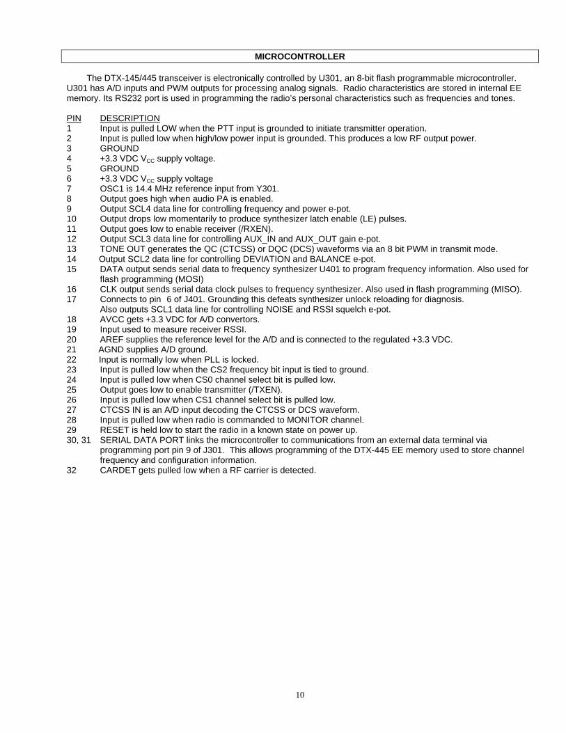
The DTX-145/445 transceiver is electronically controlled by U301, an 8-bit flash programmable microcontroller. U301 has A/D inputs and PWM outputs for processing analog signals. Radio characteristics are stored in internal EE memory. Its RS232 port is used in programming the radio’s personal characteristics such as frequencies and tones. PIN DESCRIPTION 1 Input is pulled LOW when the PTT input is grounded to initiate transmitter operation. 2 Input is pulled low when high/low power input is grounded. This produces a low RF output power. 3 GROUND 4 +3.3 VDC VCC supply voltage. 5 GROUND 6 +3.3 VDC VCC supply voltage 7 OSC1 is 14.4 MHz reference input from Y301. 8 Output goes high when audio PA is enabled. 9 Output SCL4 data line for controlling frequency and power e-pot. 10 Output drops low momentarily to produce synthesizer latch enable (LE) pulses. 11 Output goes low to enable receiver (/RXEN). 12 Output SCL3 data line for controlling AUX_IN and AUX_OUT gain e-pot. 13 TONE OUT generates the QC (CTCSS) or DQC (DCS) waveforms via an 8 bit PWM in transmit mode. 14 Output SCL2 data line for controlling DEVIATION and BALANCE e-pot. 15 DATA output sends serial data to frequency synthesizer U401 to program frequency information. Also used for
flash programming (MOSI) 16 CLK output sends serial data clock pulses to frequency synthesizer. Also used in flash programming (MISO). 17 Connects to pin 6 of J401. Grounding this defeats synthesizer unlock reloading for diagnosis. Also outputs SCL1 data line for controlling NOISE and RSSI squelch e-pot. 18 AVCC gets +3.3 VDC for A/D convertors. 19 Input used to measure receiver RSSI. 20 AREF supplies the reference level for the A/D and is connected to the regulated +3.3 VDC. 21 AGND supplies A/D ground. 22 Input is normally low when PLL is locked. 23 Input is pulled low when the CS2 frequency bit input is tied to ground. 24 Input is pulled low when CS0 channel select bit is pulled low. 25 Output goes low to enable transmitter (/TXEN). 26 Input is pulled low when CS1 channel select bit is pulled low. 27 CTCSS IN is an A/D input decoding the CTCSS or DCS waveform. 28 Input is pulled low when radio is commanded to MONITOR channel. 29 RESET is held low to start the radio in a known state on power up. 30, 31 SERIAL DATA PORT links the microcontroller to communications from an external data terminal via
programming port pin 9 of J301. This allows programming of the DTX-445 EE memory used to store channel frequency and configuration information.
32 CARDET gets pulled low when a RF carrier is detected.

11
DTX-145/445 ALIGNMENT PROCEDURE Only an authorized RF service technician should perform test and alignment of the DTX-145/445. The unit is PC adjusted.
RECOMMENDED TEST EQUIPMENT 1) 12.5 to 14 VDC 2 Amp current-limited power supply 3) Oscilloscope 2) RF Communications Test with: 4) Sine wave generator around 500 Hz - FM Deviation Meter - RF Wattmeter 5) RITRON PC Programming Kit - Frequency Counter - SINAD Measuring Device
RADIO PREPARATION 2) Connect the FM communications test set to the antenna connector. 3) Connect RITRON programming cable to radio and PC. 4) Apply 12.5 to 14 VDC to the red wire with the black to ground. 5) Run RITRON DTX software and read the radio.
RADIO ADJUSTMENT
The DTX-145/445 is preset at the factory for 5 Watts (or 8 watts) in high power and around 2 watts in low power at 12.5 VDC. The programming software includes help comments. If DTX needs to be changed or readjusted do the following:
1) Make sure that the unit is at room temperature and voltage between pin 6 and pin 15 is at least 12.5 VDC while
transmitting. There may be significant resistive losses causing voltage drop in the supply cable. 2) Set the RF communications test set to the transmit mode. Make sure equipment is calibrated including coax cable
and adapters. Note that a 1 dB cable loss will yield a 20% power loss. 3) Make sure the Hi/low power pin 5 is unconnected. This selects high power. 4) Run RITRON DTX LS programming software. 5) On the menu bar select Edit then Tune radio. 6) If starting from scratch, set up the radio in the order the buttons appear from top to bottom on the left: Frequency,
Mod Balance, Deviation, Power then User Set Up. Otherwise, adjust what is needed. 7) Click Frequency then Tune. 8) The frequency used in adjustment is displayed in the upper right corner. 9) Radio will transmit in center of band (460 MHz for DTX-445 O band). TX frequency is displayed in upper right hand
corner of form. Adjust frequency by clicking arrows or by click in space to right of sliding button (for up) or space left (for down). Button can also be dragged to position.
10) Adjusted transmitter frequency reading should be less than +/-100 Hz. Click Save when done. 11) Adjust positive and negative corrections in the same way. This calibrates the reference oscillator. 12) If the reference oscillator ages and drifts in the future, only the center frequency should need trimming. 13) Apply a 500 Hz sine wave at sufficient level to AUX_IN input (pin 7). We want the sine wave to limit and appear as
a square wave when demodulated by the service monitor. 14) Click Mod Bal then Tune and adjust for flat top on square wave. Repeat for balance high frequency. 15) Click Deviation then Tune and adjust for +/- 5 kHz. Repeat for deviation high frequency.* 16) Click Power. Notice that low and high power can be set globally or on specific channels. The factory preset is global
with high power set at 5 watts (or 8 watts) for high and 2 watts for low at the center of the band. The lower and upper power may vary a bit. Variable cap C207 (seen in the hole in the PA shield) can be used to balance low to high frequency power. Also, channel specific low and high power settings can be programmed on channels 1 through 8.
17) Make your choice of what you want to adjust and adjust it. Keep in mind when you adjust low or high power in the “all channels” section you write that same setting in all channels.
18) Click User Set Up. Here, you can adjust NOISE and RSSI squelch levels and AUX_IN and AUX_OUT gain. If both RSSI and NOISE squelch are used simultaneously, the RSSI level must be set first with the NOISE squelch disabled. Disable it by adjusting the level so high (bar to the right) that the RF level never reaches it. The NOISE and RSSI squelch levels work as an OR function. With either level exceeded, the audio will turn on. Set the RSSI level around -106 dBm and then the NOISE level around -120 dBm.** When adjusting AUX_IN level apply your
12
desired signal level to pin 7. The unit was factory preset with a 300 mVpp sine wave adjusted for +/- 3 kHz deviation. This same level will produce +/- 1.5 kHz on a narrowband channel.
19) Remember to save all settings when tuning is finished. NOTES:
*Sub audible tone deviation is automatically set to be within 600 to 900 Hz after this adjustment on wide band channels. Maximum voice and tone deviation on wide band channels will then be 4800 to 5300 Hz. Narrow band tone deviation will be 350 to 500 Hz with overall deviation of 2400 to 2650 Hz.
**The DTX-145/445 is capable of two squelch operating modes. Both can operate simultaneously. See the FM Receiver Subsystem section for theory. The units can be configured as the user requires. When a low level signal appears, the noise squelch opens when the carrier is –119 dBm or greater. When the signal appearing is –106 dBm or greater the RSSI squelch opens the audio with an even faster attack time. The above levels are factory set levels. Ambient noise will affect the level at which the RSSI should be set. The squelch level ideally should be set on the desired frequency, in the actual location the radio will be used and connected to the desired antenna. The level should be set high enough to reject most false signals. The squelch levels are the same for all channels.
If a very fast receiver decay time (or squelching after signal disappears) is needed the noise squelch should be defeated by setting it to a high level.