dspic33fj12mc201 202 flash
TRANSCRIPT

dsPIC33F/PIC24HdsPIC33F/PIC24H Flash Programming Specification
1.0 DEVICE OVERVIEWThis document defines the programming specificationfor the dsPIC33F 16-bit Digital Signal Controller (DSC)and PIC24H 16-bit Microcontroller (MCU) families. Thisprogramming specification is required only for thosedeveloping programming support for thedsPIC33F/PIC24H family. Customers using only one ofthese devices should use development tools thatalready provide support for device programming.
2.0 PROGRAMMING OVERVIEW OF THE dsPIC33F/PIC24H
There are two methods of programming thedsPIC33F/PIC24H family of devices discussed in thisprogramming specification. They are:
• In-Circuit Serial Programming™ (ICSP™) programming capability
• Enhanced In-Circuit Serial Programming
The ICSP programming method is the most directmethod to program the device; however, it is also theslower of the two methods. It provides native, low-levelprogramming capability to erase, program and verifythe chip.
The Enhanced ICSP protocol uses a faster method thattakes advantage of the programming executive, asillustrated in Figure 2-1. The programming executiveprovides all the necessary functionality to erase,program and verify the chip through a small commandset. The command set allows the programmer toprogram the dsPIC33F/PIC24H ProgrammingSpecification devices without having to deal with thelow-level programming protocols of the chip.
FIGURE 2-1: PROGRAMMING SYSTEM OVERVIEW FOR ENHANCED ICSP™
This specification is divided into major sections thatdescribe the programming methods independently.Section 3.0 “Device Programming – EnhancedICSP” describes the Enhanced ICSP method.Section 5.0 “Device Programming – ICSP” describesthe ICSP method.
2.1 Power RequirementsAll devices in the dsPIC33F/PIC24H family are dualvoltage supply designs: one supply for the core andanother for the peripherals and I/O pins. A regulator isprovided on-chip to alleviate the need for two externalvoltage supplies.
All of the dsPIC33F/PIC24H devices power their coredigital logic at a nominal 2.5V. To simplify systemdesign, all devices in the dsPIC33F/PIC24HProgramming Specification family incorporate anon-chip regulator that allows the device to run its corelogic from VDD.
The regulator provides power to the core from the otherVDD pins. A low-ESR capacitor (such as tantalum) mustbe connected to the VDDCORE pin (Figure 2-2). Thishelps to maintain the stability of the regulator. Thespecifications for core voltage and capacitance arelisted in Section 8.0 “AC/DC Characteristics andTiming Requirements”.
FIGURE 2-2: CONNECTIONS FOR THE ON-CHIP REGULATOR
dsPIC33F/PIC24H
Programmer ProgrammingExecutive
On-Chip Memory
Note: These are typical operating voltages. Referto Table 8-1 for the full operating ranges ofVDD and VDDCORE.
VDD
VDDCORE
VSS
dsPIC33F/PIC24H
CF
3.3V
© 2008 Microchip Technology Inc. DS70152F-page 1

dsPIC33F/PIC24H PROGRAMMING SPECIFICATION
2.2 Program Memory Write/Erase Requirements
The program Flash memory on the dsPIC33F/PIC24Hhas a specific write/erase requirement that must beadhered to, for proper device operation. The rule is thatany given word in memory must not be written withoutfirst erasing the page in which it is located. Thus, theeasiest way to conform to this rule is to write all the datain a programming block within one write cycle. Theprogramming methods specified in this documentcomply with this requirement.
2.3 Pins Used During ProgrammingThe pins that are used for programming are listed inTable 2-1.
TABLE 2-1: PINS USED DURING PROGRAMMING
Note: Any development tool that modifies theconfiguration memory ondsPIC33FJ06GS101/102/202 anddsPIC33FJ16GS402/404/502/504 devicesmust take care to preserve the datacontained in the last six words ofconfiguration memory.
Note: A program memory word can beprogrammed twice before an erase, butonly if (a) the same data is used in bothprogram operations or (b) bits containing‘1’ are set to ‘0’ but no ‘0’ is set to ‘1’.
Note: Refer to the specific device data sheet forcomplete pin diagrams of thedsPIC33F/PIC24H devices.
Pin NameDuring Programming
Pin Name Pin Type Pin Description
MCLR MCLR P Programming EnableVDD and AVDD(1) VDD P Power SupplyVSS and AVSS(1) VSS P GroundVDDCORE VDDCORE P Regulated Power Supply for CorePGC1 PGC1 I Primary Programming Pin Pair: Serial Clock PGD1 PGD1 I/O Primary Programming Pin Pair: Serial Data PGC2 PGC2 I Secondary Programming Pin Pair: Serial Clock PGD2 PGD2 I/O Secondary Programming Pin Pair: Serial Data PGC3 PGC3 I Tertiary Programming Pin Pair: Serial Clock PGD3 PGD3 I/O Tertiary Programming Pin Pair: Serial Data Legend: I = Input, O = Output, P = PowerNote 1: All power supply and ground pins must be connected, including analog supplies (AVDD) and ground
(AVSS).
DS70152F-page 2 © 2008 Microchip Technology Inc.

dsPIC33F/PIC24H PROGRAMMING SPECIFICATION
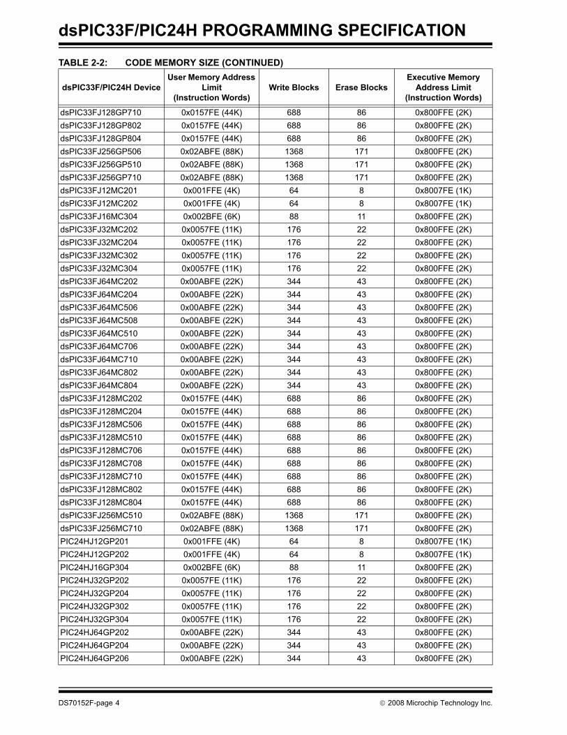
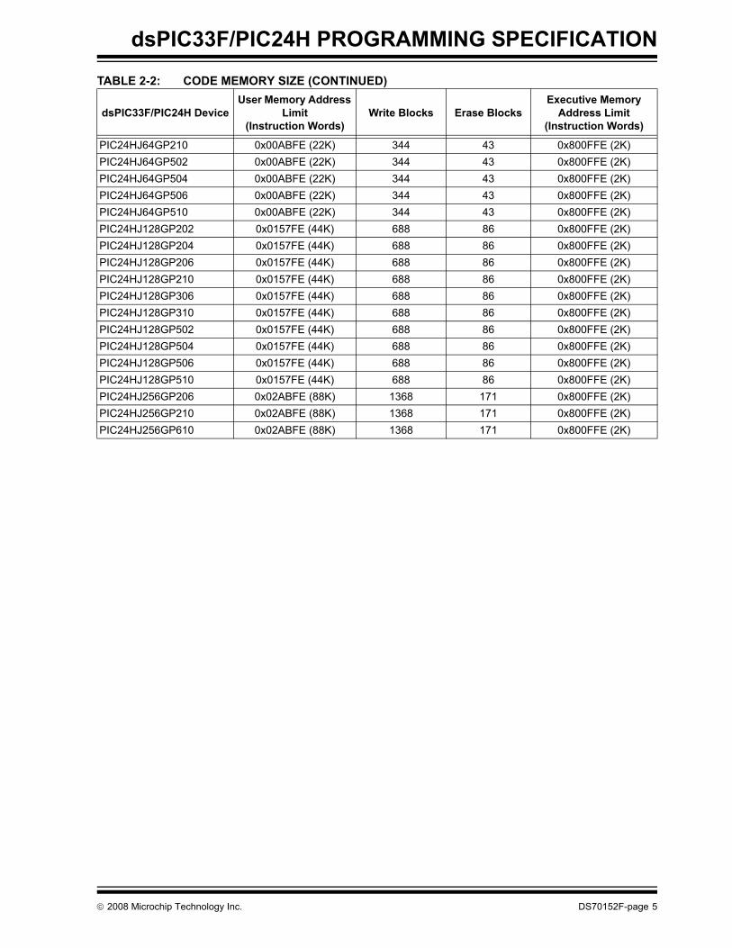
2.4 Memory MapThe program memory map extends from 0x0 to0xFFFFFE. Code storage is located at the base of thememory map and supports up to 88K instructions(about 256 Kbytes). Table 2-2 shows the programmemory size and number of erase and program blockspresent in each device variant. Each erase block orpage contains 512 instructions and each program blockor row, contains 64 instructions.
Locations 0x800000 through 0x800FFE are reservedfor executive code memory. This region stores theprogramming executive and the debuggingexecutive. The programming executive is used for
device programming and the debug executive isused for in-circuit debugging. This region of memorycannot be used to store user code.
Locations 0xF80000 through 0xF80017 are reservedfor the device Configuration registers.
Locations 0xFF0000 and 0xFF0002 are reserved forthe Device ID Word registers. These bits can be usedby the programmer to identify which device type isbeing programmed. They are described in Section 7.0“Device ID”. The Device ID registers read outnormally, even after code protection is applied.
Figure 2-3 shows the memory map for thedsPIC33F/PIC24H family variants.
TABLE 2-2: CODE MEMORY SIZE
dsPIC33F/PIC24H DeviceUser Memory Address
Limit(Instruction Words)
Write Blocks Erase BlocksExecutive Memory
Address Limit (Instruction Words)
dsPIC33FJ06GS101 0x000FFE (2K) 32 4 0x8007FE (1K)dsPIC33FJ06GS102 0x000FFE (2K) 32 4 0x8007FE (1K)dsPIC33FJ06GS202 0x000FFE (2K) 32 4 0x8007FE (1K)dsPIC33FJ16GS402 0x0028FE (6K) 88 11 0x8007FE (1K)dsPIC33FJ16GS404 0x0028FE (6K) 88 11 0x8007FE (1K)dsPIC33FJ16GS502 0x0028FE (6K) 88 11 0x8007FE (1K)dsPIC33FJ16GS504 0x0028FE (6K) 88 11 0x8007FE (1K)dsPIC33FJ12GP201 0x001FFE (4K) 64 8 0x8007FE (1K)dsPIC33FJ12GP202 0x001FFE (4K) 64 8 0x8007FE (1K)dsPIC33FJ16GP304 0x002BFE (6K) 88 11 0x800FFE (2K)dsPIC33FJ32GP202 0x0057FE (11K) 176 22 0x800FFE (2K)dsPIC33FJ32GP204 0x0057FE (11K) 176 22 0x800FFE (2K)dsPIC33FJ32GP302 0x0057FE (11K) 176 22 0x800FFE (2K)dsPIC33FJ32GP304 0x0057FE (11K) 176 22 0x800FFE (2K)dsPIC33FJ64GP202 0x00ABFE (22K) 344 43 0x800FFE (2K)dsPIC33FJ64GP204 0x00ABFE (22K) 344 43 0x800FFE (2K)dsPIC33FJ64GP206 0x00ABFE (22K) 344 43 0x800FFE (2K)dsPIC33FJ64GP306 0x00ABFE (22K) 344 43 0x800FFE (2K)dsPIC33FJ64GP310 0x00ABFE (22K) 344 43 0x800FFE (2K)dsPIC33FJ64GP706 0x00ABFE (22K) 344 43 0x800FFE (2K)dsPIC33FJ64GP708 0x00ABFE (22K) 344 43 0x800FFE (2K)dsPIC33FJ64GP710 0x00ABFE (22K) 344 43 0x800FFE (2K)dsPIC33FJ64GP802 0x00ABFE (22K) 344 43 0x800FFE (2K)dsPIC33FJ64GP804 0x00ABFE (22K) 344 43 0x800FFE (2K)dsPIC33FJ128GP202 0x0157FE (44K) 688 86 0x800FFE (2K)dsPIC33FJ128GP204 0x0157FE (44K) 688 86 0x800FFE (2K)dsPIC33FJ128GP206 0x0157FE (44K) 688 86 0x800FFE (2K)dsPIC33FJ128GP306 0x0157FE (44K) 688 86 0x800FFE (2K)dsPIC33FJ128GP310 0x0157FE (44K) 688 86 0x800FFE (2K)dsPIC33FJ128GP706 0x0157FE (44K) 688 86 0x800FFE (2K)dsPIC33FJ128GP708 0x0157FE (44K) 688 86 0x800FFE (2K)
© 2008 Microchip Technology Inc. DS70152F-page 3
dsPIC33F/PIC24H PROGRAMMING SPECIFICATION
dsPIC33FJ128GP710 0x0157FE (44K) 688 86 0x800FFE (2K)dsPIC33FJ128GP802 0x0157FE (44K) 688 86 0x800FFE (2K)dsPIC33FJ128GP804 0x0157FE (44K) 688 86 0x800FFE (2K)dsPIC33FJ256GP506 0x02ABFE (88K) 1368 171 0x800FFE (2K)dsPIC33FJ256GP510 0x02ABFE (88K) 1368 171 0x800FFE (2K)dsPIC33FJ256GP710 0x02ABFE (88K) 1368 171 0x800FFE (2K)dsPIC33FJ12MC201 0x001FFE (4K) 64 8 0x8007FE (1K)dsPIC33FJ12MC202 0x001FFE (4K) 64 8 0x8007FE (1K)dsPIC33FJ16MC304 0x002BFE (6K) 88 11 0x800FFE (2K)dsPIC33FJ32MC202 0x0057FE (11K) 176 22 0x800FFE (2K)dsPIC33FJ32MC204 0x0057FE (11K) 176 22 0x800FFE (2K)dsPIC33FJ32MC302 0x0057FE (11K) 176 22 0x800FFE (2K)dsPIC33FJ32MC304 0x0057FE (11K) 176 22 0x800FFE (2K)dsPIC33FJ64MC202 0x00ABFE (22K) 344 43 0x800FFE (2K)dsPIC33FJ64MC204 0x00ABFE (22K) 344 43 0x800FFE (2K)dsPIC33FJ64MC506 0x00ABFE (22K) 344 43 0x800FFE (2K)dsPIC33FJ64MC508 0x00ABFE (22K) 344 43 0x800FFE (2K)dsPIC33FJ64MC510 0x00ABFE (22K) 344 43 0x800FFE (2K)dsPIC33FJ64MC706 0x00ABFE (22K) 344 43 0x800FFE (2K)dsPIC33FJ64MC710 0x00ABFE (22K) 344 43 0x800FFE (2K)dsPIC33FJ64MC802 0x00ABFE (22K) 344 43 0x800FFE (2K)dsPIC33FJ64MC804 0x00ABFE (22K) 344 43 0x800FFE (2K)dsPIC33FJ128MC202 0x0157FE (44K) 688 86 0x800FFE (2K)dsPIC33FJ128MC204 0x0157FE (44K) 688 86 0x800FFE (2K)dsPIC33FJ128MC506 0x0157FE (44K) 688 86 0x800FFE (2K)dsPIC33FJ128MC510 0x0157FE (44K) 688 86 0x800FFE (2K)dsPIC33FJ128MC706 0x0157FE (44K) 688 86 0x800FFE (2K)dsPIC33FJ128MC708 0x0157FE (44K) 688 86 0x800FFE (2K)dsPIC33FJ128MC710 0x0157FE (44K) 688 86 0x800FFE (2K)dsPIC33FJ128MC802 0x0157FE (44K) 688 86 0x800FFE (2K)dsPIC33FJ128MC804 0x0157FE (44K) 688 86 0x800FFE (2K)dsPIC33FJ256MC510 0x02ABFE (88K) 1368 171 0x800FFE (2K)dsPIC33FJ256MC710 0x02ABFE (88K) 1368 171 0x800FFE (2K)PIC24HJ12GP201 0x001FFE (4K) 64 8 0x8007FE (1K)PIC24HJ12GP202 0x001FFE (4K) 64 8 0x8007FE (1K)PIC24HJ16GP304 0x002BFE (6K) 88 11 0x800FFE (2K)PIC24HJ32GP202 0x0057FE (11K) 176 22 0x800FFE (2K)PIC24HJ32GP204 0x0057FE (11K) 176 22 0x800FFE (2K)PIC24HJ32GP302 0x0057FE (11K) 176 22 0x800FFE (2K)PIC24HJ32GP304 0x0057FE (11K) 176 22 0x800FFE (2K)PIC24HJ64GP202 0x00ABFE (22K) 344 43 0x800FFE (2K)PIC24HJ64GP204 0x00ABFE (22K) 344 43 0x800FFE (2K)PIC24HJ64GP206 0x00ABFE (22K) 344 43 0x800FFE (2K)
TABLE 2-2: CODE MEMORY SIZE (CONTINUED)
dsPIC33F/PIC24H DeviceUser Memory Address
Limit(Instruction Words)
Write Blocks Erase BlocksExecutive Memory
Address Limit (Instruction Words)
DS70152F-page 4 © 2008 Microchip Technology Inc.
dsPIC33F/PIC24H PROGRAMMING SPECIFICATION
PIC24HJ64GP210 0x00ABFE (22K) 344 43 0x800FFE (2K)PIC24HJ64GP502 0x00ABFE (22K) 344 43 0x800FFE (2K)PIC24HJ64GP504 0x00ABFE (22K) 344 43 0x800FFE (2K)PIC24HJ64GP506 0x00ABFE (22K) 344 43 0x800FFE (2K)PIC24HJ64GP510 0x00ABFE (22K) 344 43 0x800FFE (2K)PIC24HJ128GP202 0x0157FE (44K) 688 86 0x800FFE (2K)PIC24HJ128GP204 0x0157FE (44K) 688 86 0x800FFE (2K)PIC24HJ128GP206 0x0157FE (44K) 688 86 0x800FFE (2K)PIC24HJ128GP210 0x0157FE (44K) 688 86 0x800FFE (2K)PIC24HJ128GP306 0x0157FE (44K) 688 86 0x800FFE (2K)PIC24HJ128GP310 0x0157FE (44K) 688 86 0x800FFE (2K)PIC24HJ128GP502 0x0157FE (44K) 688 86 0x800FFE (2K)PIC24HJ128GP504 0x0157FE (44K) 688 86 0x800FFE (2K)PIC24HJ128GP506 0x0157FE (44K) 688 86 0x800FFE (2K)PIC24HJ128GP510 0x0157FE (44K) 688 86 0x800FFE (2K)PIC24HJ256GP206 0x02ABFE (88K) 1368 171 0x800FFE (2K)PIC24HJ256GP210 0x02ABFE (88K) 1368 171 0x800FFE (2K)PIC24HJ256GP610 0x02ABFE (88K) 1368 171 0x800FFE (2K)
TABLE 2-2: CODE MEMORY SIZE (CONTINUED)
dsPIC33F/PIC24H DeviceUser Memory Address
Limit(Instruction Words)
Write Blocks Erase BlocksExecutive Memory
Address Limit (Instruction Words)
© 2008 Microchip Technology Inc. DS70152F-page 5

dsPIC33F/PIC24H PROGRAMMING SPECIFICATION
FIGURE 2-3: PROGRAM MEMORY MAP
Use
r Mem
ory
Spac
e
0x000000
Configuration Registers
Code Memory
0x02AC000x02ABFE
Con
figur
atio
n M
emor
ySp
ace
(87552 x 24-bit)
0x800000
0xF80000(12 x 8-bit) 0xF80017
0xF80018
Device ID0xFEFFFE0xFF0000
0xFFFFFE
Reserved
0xF7FFFE
Reserved
0x800FFE0x801000
Executive Code Memory
0x7FFFFE
Reserved
0xFF00020xFF0004Reserved
(2 x 16-bit)
Note: The address boundaries for user Flash and Executive code memory are device dependent.
User Flash
(2048 x 24-bit)
DS70152F-page 6 © 2008 Microchip Technology Inc.

dsPIC33F/PIC24H PROGRAMMING SPECIFICATION
3.0 DEVICE PROGRAMMING – ENHANCED ICSP
This section discusses programming the devicethrough Enhanced ICSP and the programmingexecutive. The programming executive resides inexecutive memory (separate from code memory) and isexecuted when Enhanced ICSP Programming mode isentered. The programming executive provides themechanism for the programmer (host device) toprogram and verify the dsPIC33F/PIC24HProgramming Specification family devices using asimple command set and communication protocol.There are several basic functions provided by theprogramming executive:
• Read Memory• Erase Memory• Program Memory• Blank Check• Read Executive Firmware Revision
The programming executive performs the low-leveltasks required for erasing, programming and verifyinga device. This allows the programmer to program thedevice by issuing the appropriate commands and data.Table 3-1 summarizes the commands. A detaileddescription for each command is provided inSection 4.2 “Programming Executive Commands”.
TABLE 3-1: COMMAND SET SUMMARY
The programming executive uses the device’s dataRAM for variable storage and program execution. Afterthe programming executive is run, no assumptionsshould be made about the contents of data RAM.
3.1 Overview of the Programming Process
Figure 3-1 shows the high-level overview of theprogramming process. After entering Enhanced ICSPmode, the programming executive is verified. Next, thedevice is erased. Then, the code memory isprogrammed, followed by the nonvolatile deviceConfiguration registers. Code memory (including theConfiguration registers) is then verified to ensure thatprogramming was successful.
After the programming executive has been verifiedin memory (or loaded if not present), thedsPIC33F/PIC24H Programming Specification can beprogrammed using the command set shown inTable 3-1.
FIGURE 3-1: HIGH-LEVEL ENHANCED ICSP™ PROGRAMMING FLOW
Command Description
SCHECK Sanity check.READC Read Configuration registers or Device
ID registers.READP Read code memory. PROGC Program a Configuration register and
verify.PROGP Program one row of code memory and
verify.PROGW Program one word of code memory
and verify.QBLANK Query if the code memory is blank.QVER Query the software version.
Start
End
Perform BulkErase
Program Memory
Verify Program
Enter Enhanced ICSP™
Program Configuration Bits
Verify Configuration Bits
Exit Enhanced ICSP
© 2008 Microchip Technology Inc. DS70152F-page 7
dsPIC33F/PIC24H PROGRAMMING SPECIFICATION
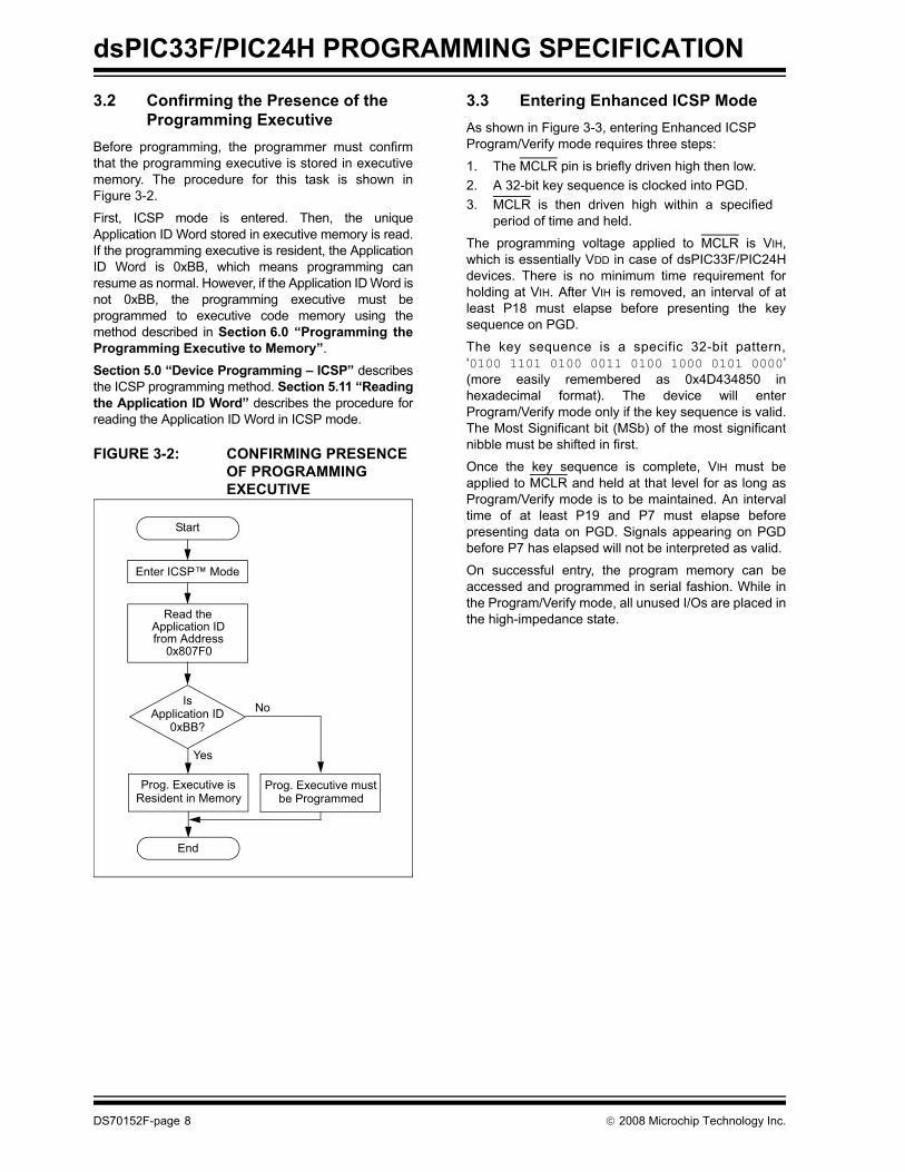
3.2 Confirming the Presence of the Programming Executive
Before programming, the programmer must confirmthat the programming executive is stored in executivememory. The procedure for this task is shown inFigure 3-2.
First, ICSP mode is entered. Then, the uniqueApplication ID Word stored in executive memory is read.If the programming executive is resident, the ApplicationID Word is 0xBB, which means programming canresume as normal. However, if the Application ID Word isnot 0xBB, the programming executive must beprogrammed to executive code memory using themethod described in Section 6.0 “Programming theProgramming Executive to Memory”.
Section 5.0 “Device Programming – ICSP” describesthe ICSP programming method. Section 5.11 “Readingthe Application ID Word” describes the procedure forreading the Application ID Word in ICSP mode.
FIGURE 3-2: CONFIRMING PRESENCE OF PROGRAMMING EXECUTIVE
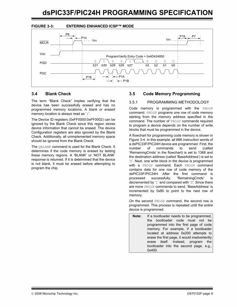
3.3 Entering Enhanced ICSP ModeAs shown in Figure 3-3, entering Enhanced ICSP Program/Verify mode requires three steps:
1. The MCLR pin is briefly driven high then low.2. A 32-bit key sequence is clocked into PGD.3. MCLR is then driven high within a specified
period of time and held.
The programming voltage applied to MCLR is VIH,which is essentially VDD in case of dsPIC33F/PIC24Hdevices. There is no minimum time requirement forholding at VIH. After VIH is removed, an interval of atleast P18 must elapse before presenting the keysequence on PGD.
The key sequence is a specific 32-bit pattern,‘0100 1101 0100 0011 0100 1000 0101 0000’(more easily remembered as 0x4D434850 inhexadecimal format). The device will enterProgram/Verify mode only if the key sequence is valid.The Most Significant bit (MSb) of the most significantnibble must be shifted in first.
Once the key sequence is complete, VIH must beapplied to MCLR and held at that level for as long asProgram/Verify mode is to be maintained. An intervaltime of at least P19 and P7 must elapse beforepresenting data on PGD. Signals appearing on PGDbefore P7 has elapsed will not be interpreted as valid.
On successful entry, the program memory can beaccessed and programmed in serial fashion. While inthe Program/Verify mode, all unused I/Os are placed inthe high-impedance state.
Is
Start
Enter ICSP™ Mode
Application ID0xBB?
Resident in Memory
Yes
No
Prog. Executive is
Application IDRead the
be ProgrammedProg. Executive must
from Address0x807F0
End
DS70152F-page 8 © 2008 Microchip Technology Inc.
dsPIC33F/PIC24H PROGRAMMING SPECIFICATION
FIGURE 3-3: ENTERING ENHANCED ICSP™ MODE
3.4 Blank CheckThe term “Blank Check” implies verifying that thedevice has been successfully erased and has noprogrammed memory locations. A blank or erasedmemory location is always read as ‘1’.
The Device ID registers (0xFF0000:0xFF0002) can beignored by the Blank Check since this region storesdevice information that cannot be erased. The deviceConfiguration registers are also ignored by the BlankCheck. Additionally, all unimplemented memory spaceshould be ignored from the Blank Check.
The QBLANK command is used for the Blank Check. Itdetermines if the code memory is erased by testingthese memory regions. A ‘BLANK’ or ‘NOT BLANK’response is returned. If it is determined that the deviceis not blank, it must be erased before attempting toprogram the chip.
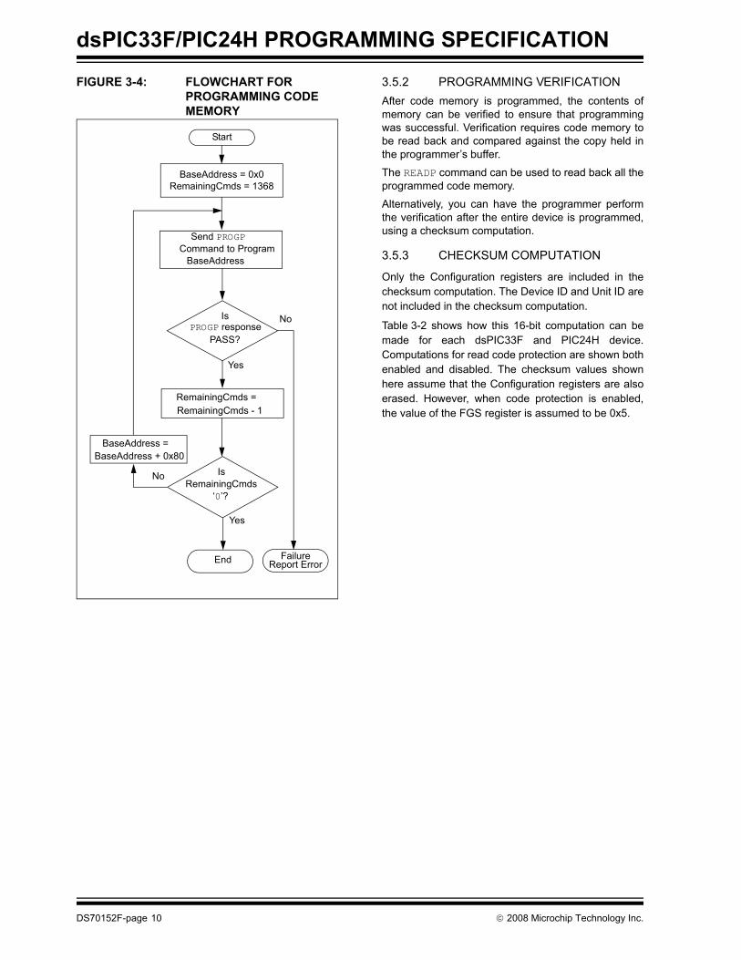
3.5 Code Memory Programming
3.5.1 PROGRAMMING METHODOLOGYCode memory is programmed with the PROGPcommand. PROGP programs one row of code memorystarting from the memory address specified in thecommand. The number of PROGP commands requiredto program a device depends on the number of writeblocks that must be programmed in the device.
A flowchart for programming code memory is shown inFigure 3-4. In this example, all 88K instruction words ofa dsPIC33F/PIC24H device are programmed. First, thenumber of commands to send (called‘RemainingCmds’ in the flowchart) is set to 1368 andthe destination address (called ‘BaseAddress’) is set to‘0’. Next, one write block in the device is programmedwith a PROGP command. Each PROGP commandcontains data for one row of code memory of thedsPIC33F/PIC24H. After the first command isprocessed successfully, ‘RemainingCmds’ isdecremented by ‘1’ and compared with ‘0’. Since thereare more PROGP commands to send, ‘BaseAddress’ isincremented by 0x80 to point to the next row ofmemory.
On the second PROGP command, the second row isprogrammed. This process is repeated until the entiredevice is programmed.
MCLR
PGD
PGC
VDD
P6P14
b31 b30 b29 b28 b27 b2 b1 b0b3...
Program/Verify Entry Code = 0x4D434850
P1AP1B
P18
P19
0 1 0 0 1 0 0 0 0
P7VIH VIH
Note: If a bootloader needs to be programmed,the bootloader code must not beprogrammed into the first page of codememory. For example, if a bootloaderlocated at address 0x200 attempts toerase the first page, it would inadvertentlyerase itself. Instead, program thebootloader into the second page, e.g.,0x400.
© 2008 Microchip Technology Inc. DS70152F-page 9
dsPIC33F/PIC24H PROGRAMMING SPECIFICATION
FIGURE 3-4: FLOWCHART FOR PROGRAMMING CODE MEMORY
3.5.2 PROGRAMMING VERIFICATIONAfter code memory is programmed, the contents ofmemory can be verified to ensure that programmingwas successful. Verification requires code memory tobe read back and compared against the copy held inthe programmer’s buffer.
The READP command can be used to read back all theprogrammed code memory.
Alternatively, you can have the programmer performthe verification after the entire device is programmed,using a checksum computation.
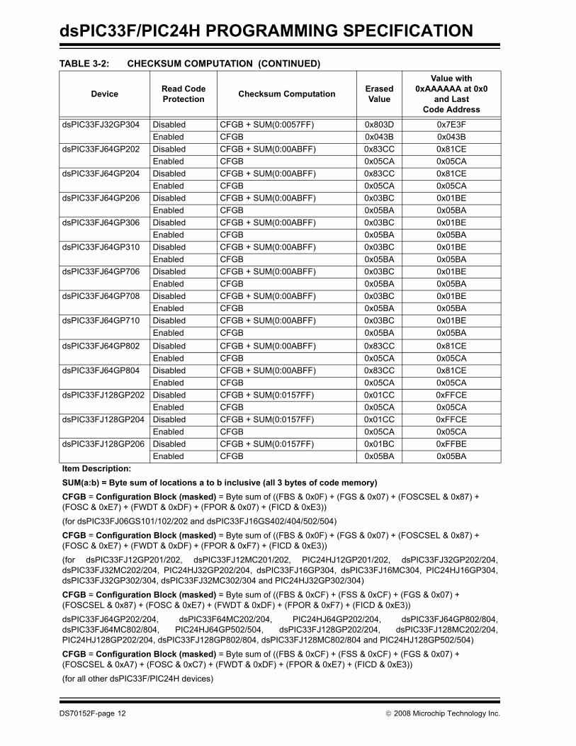
3.5.3 CHECKSUM COMPUTATION
Only the Configuration registers are included in thechecksum computation. The Device ID and Unit ID arenot included in the checksum computation.
Table 3-2 shows how this 16-bit computation can bemade for each dsPIC33F and PIC24H device.Computations for read code protection are shown bothenabled and disabled. The checksum values shownhere assume that the Configuration registers are alsoerased. However, when code protection is enabled,the value of the FGS register is assumed to be 0x5.
BaseAddress = 0x0RemainingCmds = 1368
Start
FailureReport Error
End
Yes
No
RemainingCmds =RemainingCmds - 1
Yes
PASS?
No
BaseAddressCommand to Program
Send PROGP
RemainingCmdsIs
‘0’?
BaseAddress + 0x80BaseAddress =
PROGP responseIs
DS70152F-page 10 © 2008 Microchip Technology Inc.

dsPIC33F/PIC24H PROGRAMMING SPECIFICATION
TABLE 3-2: CHECKSUM COMPUTATION
Device Read CodeProtection Checksum Computation Erased
Value
Value with0xAAAAAA at 0x0
and LastCode Address
dsPIC33FJ06GS101 Disabled CFGB + SUM(0:000FFF) 0xEB55 0xE957Enabled CFGB 0x0353 0x0353
dsPIC33FJ06GS102 Disabled CFGB + SUM(0:000FFF) 0xEB55 0xE957Enabled CFGB 0x0353 0x0353
dsPIC33FJ06GS202 Disabled CFGB + SUM(0:000FFF) 0xEB55 0xE957Enabled CFGB 0x0353 0x0353
dsPIC33FJ16GS402 Disabled CFGB + SUM(0:002BFF) 0xC155 0xBF57Enabled CFGB 0x0353 0x0353
dsPIC33FJ16GS404 Disabled CFGB + SUM(0:002BFF) 0xC155 0xBF57Enabled CFGB 0x0353 0x0353
dsPIC33FJ16GS502 Disabled CFGB + SUM(0:002BFF) 0xC155 0xBF57Enabled CFGB 0x0353 0x0353
dsPIC33FJ16GS504 Disabled CFGB + SUM(0:002BFF) 0xC155 0xBF57Enabled CFGB 0x0353 0x0353
dsPIC33FJ12GP201 Disabled CFGB + SUM(0:001FFF) 0xD43D 0xD23FEnabled CFGB 0x043B 0x043B
dsPIC33FJ12GP202 Disabled CFGB + SUM(0:001FFF) 0xD43D 0xD23FEnabled CFGB 0x043B 0x043B
dsPIC33FJ16GP304 Disabled CFGB + SUM(0:002BFF) 0xC23D 0xC03FEnabled CFGB 0x043B 0x043B
dsPIC33FJ32GP202 Disabled CFGB + SUM(0:0057FF) 0x803D 0x7E3FEnabled CFGB 0x043B 0x043B
dsPIC33FJ32GP204 Disabled CFGB + SUM(0:0057FF) 0x803D 0x7E3FEnabled CFGB 0x043B 0x043B
dsPIC33FJ32GP302 Disabled CFGB + SUM(0:0057FF) 0x803D 0x7E3FEnabled CFGB 0x043B 0x043B
Item Description:SUM(a:b) = Byte sum of locations a to b inclusive (all 3 bytes of code memory)CFGB = Configuration Block (masked) = Byte sum of ((FBS & 0x0F) + (FGS & 0x07) + (FOSCSEL & 0x87) + (FOSC & 0xE7) + (FWDT & 0xDF) + (FPOR & 0x07) + (FICD & 0xE3))
(for dsPIC33FJ06GS101/102/202 and dsPIC33FJ16GS402/404/502/504)
CFGB = Configuration Block (masked) = Byte sum of ((FBS & 0x0F) + (FGS & 0x07) + (FOSCSEL & 0x87) + (FOSC & 0xE7) + (FWDT & 0xDF) + (FPOR & 0xF7) + (FICD & 0xE3))
(for dsPIC33FJ12GP201/202, dsPIC33FJ12MC201/202, PIC24HJ12GP201/202, dsPIC33FJ32GP202/204,dsPIC33FJ32MC202/204, PIC24HJ32GP202/204, dsPIC33FJ16GP304, dsPIC33FJ16MC304, PIC24HJ16GP304,dsPIC33FJ32GP302/304, dsPIC33FJ32MC302/304 and PIC24HJ32GP302/304)
CFGB = Configuration Block (masked) = Byte sum of ((FBS & 0xCF) + (FSS & 0xCF) + (FGS & 0x07) + (FOSCSEL & 0x87) + (FOSC & 0xE7) + (FWDT & 0xDF) + (FPOR & 0xF7) + (FICD & 0xE3))
dsPIC33FJ64GP202/204, dsPIC33F64MC202/204, PIC24HJ64GP202/204, dsPIC33FJ64GP802/804,dsPIC33FJ64MC802/804, PIC24HJ64GP502/504, dsPIC33FJ128GP202/204, dsPIC33FJ128MC202/204,PIC24HJ128GP202/204, dsPIC33FJ128GP802/804, dsPIC33FJ128MC802/804 and PIC24HJ128GP502/504)
CFGB = Configuration Block (masked) = Byte sum of ((FBS & 0xCF) + (FSS & 0xCF) + (FGS & 0x07) + (FOSCSEL & 0xA7) + (FOSC & 0xC7) + (FWDT & 0xDF) + (FPOR & 0xE7) + (FICD & 0xE3))
(for all other dsPIC33F/PIC24H devices)
© 2008 Microchip Technology Inc. DS70152F-page 11
dsPIC33F/PIC24H PROGRAMMING SPECIFICATION
dsPIC33FJ32GP304 Disabled CFGB + SUM(0:0057FF) 0x803D 0x7E3FEnabled CFGB 0x043B 0x043B
dsPIC33FJ64GP202 Disabled CFGB + SUM(0:00ABFF) 0x83CC 0x81CEEnabled CFGB 0x05CA 0x05CA
dsPIC33FJ64GP204 Disabled CFGB + SUM(0:00ABFF) 0x83CC 0x81CEEnabled CFGB 0x05CA 0x05CA
dsPIC33FJ64GP206 Disabled CFGB + SUM(0:00ABFF) 0x03BC 0x01BEEnabled CFGB 0x05BA 0x05BA
dsPIC33FJ64GP306 Disabled CFGB + SUM(0:00ABFF) 0x03BC 0x01BEEnabled CFGB 0x05BA 0x05BA
dsPIC33FJ64GP310 Disabled CFGB + SUM(0:00ABFF) 0x03BC 0x01BEEnabled CFGB 0x05BA 0x05BA
dsPIC33FJ64GP706 Disabled CFGB + SUM(0:00ABFF) 0x03BC 0x01BEEnabled CFGB 0x05BA 0x05BA
dsPIC33FJ64GP708 Disabled CFGB + SUM(0:00ABFF) 0x03BC 0x01BEEnabled CFGB 0x05BA 0x05BA
dsPIC33FJ64GP710 Disabled CFGB + SUM(0:00ABFF) 0x03BC 0x01BEEnabled CFGB 0x05BA 0x05BA
dsPIC33FJ64GP802 Disabled CFGB + SUM(0:00ABFF) 0x83CC 0x81CEEnabled CFGB 0x05CA 0x05CA
dsPIC33FJ64GP804 Disabled CFGB + SUM(0:00ABFF) 0x83CC 0x81CEEnabled CFGB 0x05CA 0x05CA
dsPIC33FJ128GP202 Disabled CFGB + SUM(0:0157FF) 0x01CC 0xFFCEEnabled CFGB 0x05CA 0x05CA
dsPIC33FJ128GP204 Disabled CFGB + SUM(0:0157FF) 0x01CC 0xFFCEEnabled CFGB 0x05CA 0x05CA
dsPIC33FJ128GP206 Disabled CFGB + SUM(0:0157FF) 0x01BC 0xFFBEEnabled CFGB 0x05BA 0x05BA
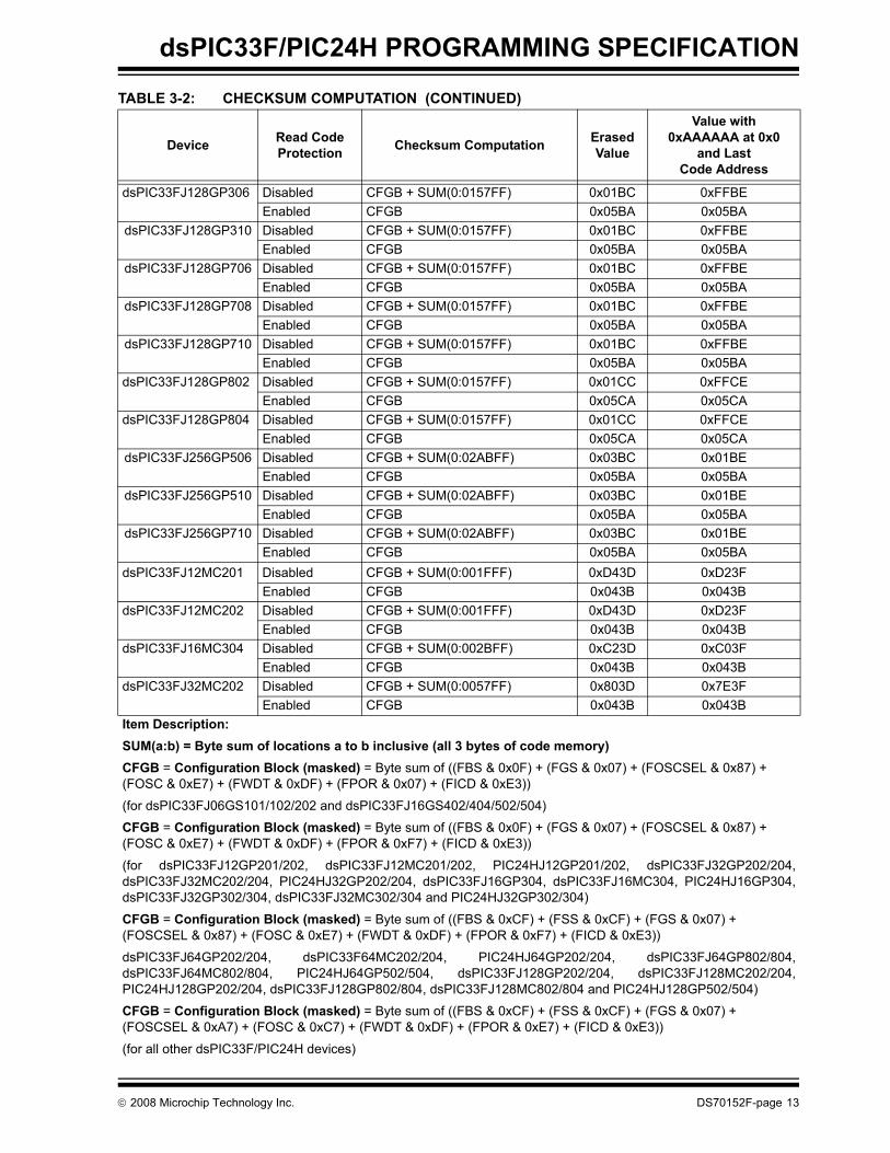
TABLE 3-2: CHECKSUM COMPUTATION (CONTINUED)
Device Read CodeProtection Checksum Computation Erased
Value
Value with0xAAAAAA at 0x0
and LastCode Address
Item Description:SUM(a:b) = Byte sum of locations a to b inclusive (all 3 bytes of code memory)CFGB = Configuration Block (masked) = Byte sum of ((FBS & 0x0F) + (FGS & 0x07) + (FOSCSEL & 0x87) + (FOSC & 0xE7) + (FWDT & 0xDF) + (FPOR & 0x07) + (FICD & 0xE3))
(for dsPIC33FJ06GS101/102/202 and dsPIC33FJ16GS402/404/502/504)
CFGB = Configuration Block (masked) = Byte sum of ((FBS & 0x0F) + (FGS & 0x07) + (FOSCSEL & 0x87) + (FOSC & 0xE7) + (FWDT & 0xDF) + (FPOR & 0xF7) + (FICD & 0xE3))
(for dsPIC33FJ12GP201/202, dsPIC33FJ12MC201/202, PIC24HJ12GP201/202, dsPIC33FJ32GP202/204,dsPIC33FJ32MC202/204, PIC24HJ32GP202/204, dsPIC33FJ16GP304, dsPIC33FJ16MC304, PIC24HJ16GP304,dsPIC33FJ32GP302/304, dsPIC33FJ32MC302/304 and PIC24HJ32GP302/304)
CFGB = Configuration Block (masked) = Byte sum of ((FBS & 0xCF) + (FSS & 0xCF) + (FGS & 0x07) + (FOSCSEL & 0x87) + (FOSC & 0xE7) + (FWDT & 0xDF) + (FPOR & 0xF7) + (FICD & 0xE3))
dsPIC33FJ64GP202/204, dsPIC33F64MC202/204, PIC24HJ64GP202/204, dsPIC33FJ64GP802/804,dsPIC33FJ64MC802/804, PIC24HJ64GP502/504, dsPIC33FJ128GP202/204, dsPIC33FJ128MC202/204,PIC24HJ128GP202/204, dsPIC33FJ128GP802/804, dsPIC33FJ128MC802/804 and PIC24HJ128GP502/504)
CFGB = Configuration Block (masked) = Byte sum of ((FBS & 0xCF) + (FSS & 0xCF) + (FGS & 0x07) + (FOSCSEL & 0xA7) + (FOSC & 0xC7) + (FWDT & 0xDF) + (FPOR & 0xE7) + (FICD & 0xE3))
(for all other dsPIC33F/PIC24H devices)
DS70152F-page 12 © 2008 Microchip Technology Inc.
dsPIC33F/PIC24H PROGRAMMING SPECIFICATION
dsPIC33FJ128GP306 Disabled CFGB + SUM(0:0157FF) 0x01BC 0xFFBEEnabled CFGB 0x05BA 0x05BA
dsPIC33FJ128GP310 Disabled CFGB + SUM(0:0157FF) 0x01BC 0xFFBEEnabled CFGB 0x05BA 0x05BA
dsPIC33FJ128GP706 Disabled CFGB + SUM(0:0157FF) 0x01BC 0xFFBEEnabled CFGB 0x05BA 0x05BA
dsPIC33FJ128GP708 Disabled CFGB + SUM(0:0157FF) 0x01BC 0xFFBEEnabled CFGB 0x05BA 0x05BA
dsPIC33FJ128GP710 Disabled CFGB + SUM(0:0157FF) 0x01BC 0xFFBEEnabled CFGB 0x05BA 0x05BA
dsPIC33FJ128GP802 Disabled CFGB + SUM(0:0157FF) 0x01CC 0xFFCEEnabled CFGB 0x05CA 0x05CA
dsPIC33FJ128GP804 Disabled CFGB + SUM(0:0157FF) 0x01CC 0xFFCEEnabled CFGB 0x05CA 0x05CA
dsPIC33FJ256GP506 Disabled CFGB + SUM(0:02ABFF) 0x03BC 0x01BEEnabled CFGB 0x05BA 0x05BA
dsPIC33FJ256GP510 Disabled CFGB + SUM(0:02ABFF) 0x03BC 0x01BEEnabled CFGB 0x05BA 0x05BA
dsPIC33FJ256GP710 Disabled CFGB + SUM(0:02ABFF) 0x03BC 0x01BEEnabled CFGB 0x05BA 0x05BA
dsPIC33FJ12MC201 Disabled CFGB + SUM(0:001FFF) 0xD43D 0xD23FEnabled CFGB 0x043B 0x043B
dsPIC33FJ12MC202 Disabled CFGB + SUM(0:001FFF) 0xD43D 0xD23FEnabled CFGB 0x043B 0x043B
dsPIC33FJ16MC304 Disabled CFGB + SUM(0:002BFF) 0xC23D 0xC03FEnabled CFGB 0x043B 0x043B
dsPIC33FJ32MC202 Disabled CFGB + SUM(0:0057FF) 0x803D 0x7E3FEnabled CFGB 0x043B 0x043B
TABLE 3-2: CHECKSUM COMPUTATION (CONTINUED)
Device Read CodeProtection Checksum Computation Erased
Value
Value with0xAAAAAA at 0x0
and LastCode Address
Item Description:SUM(a:b) = Byte sum of locations a to b inclusive (all 3 bytes of code memory)CFGB = Configuration Block (masked) = Byte sum of ((FBS & 0x0F) + (FGS & 0x07) + (FOSCSEL & 0x87) + (FOSC & 0xE7) + (FWDT & 0xDF) + (FPOR & 0x07) + (FICD & 0xE3))
(for dsPIC33FJ06GS101/102/202 and dsPIC33FJ16GS402/404/502/504)
CFGB = Configuration Block (masked) = Byte sum of ((FBS & 0x0F) + (FGS & 0x07) + (FOSCSEL & 0x87) + (FOSC & 0xE7) + (FWDT & 0xDF) + (FPOR & 0xF7) + (FICD & 0xE3))
(for dsPIC33FJ12GP201/202, dsPIC33FJ12MC201/202, PIC24HJ12GP201/202, dsPIC33FJ32GP202/204,dsPIC33FJ32MC202/204, PIC24HJ32GP202/204, dsPIC33FJ16GP304, dsPIC33FJ16MC304, PIC24HJ16GP304,dsPIC33FJ32GP302/304, dsPIC33FJ32MC302/304 and PIC24HJ32GP302/304)
CFGB = Configuration Block (masked) = Byte sum of ((FBS & 0xCF) + (FSS & 0xCF) + (FGS & 0x07) + (FOSCSEL & 0x87) + (FOSC & 0xE7) + (FWDT & 0xDF) + (FPOR & 0xF7) + (FICD & 0xE3))
dsPIC33FJ64GP202/204, dsPIC33F64MC202/204, PIC24HJ64GP202/204, dsPIC33FJ64GP802/804,dsPIC33FJ64MC802/804, PIC24HJ64GP502/504, dsPIC33FJ128GP202/204, dsPIC33FJ128MC202/204,PIC24HJ128GP202/204, dsPIC33FJ128GP802/804, dsPIC33FJ128MC802/804 and PIC24HJ128GP502/504)
CFGB = Configuration Block (masked) = Byte sum of ((FBS & 0xCF) + (FSS & 0xCF) + (FGS & 0x07) + (FOSCSEL & 0xA7) + (FOSC & 0xC7) + (FWDT & 0xDF) + (FPOR & 0xE7) + (FICD & 0xE3))
(for all other dsPIC33F/PIC24H devices)
© 2008 Microchip Technology Inc. DS70152F-page 13

dsPIC33F/PIC24H PROGRAMMING SPECIFICATION
dsPIC33FJ32MC204 Disabled CFGB + SUM(0:0057FF) 0x803D 0x7E3FEnabled CFGB 0x043B 0x043B
dsPIC33FJ32MC302 Disabled CFGB + SUM(0:0057FF) 0x803D 0x7E3FEnabled CFGB 0x043B 0x043B
dsPIC33FJ32MC304 Disabled CFGB + SUM(0:0057FF) 0x803D 0x7E3FEnabled CFGB 0x043B 0x043B
dsPIC33FJ64MC202 Disabled CFGB + SUM(0:00ABFF) 0x83CC 0x81CEEnabled CFGB 0x05CA 0x05CA
dsPIC33FJ64MC204 Disabled CFGB + SUM(0:00ABFF) 0x83CC 0x81CEEnabled CFGB 0x05CA 0x05CA
dsPIC33FJ64MC506 Disabled CFGB + SUM(0:00ABFF) 0x03BC 0x01BEEnabled CFGB 0x05BA 0x05BA
dsPIC33FJ64MC508 Disabled CFGB + SUM(0:00ABFF) 0x03BC 0x01BEEnabled CFGB 0x05BA 0x05BA
dsPIC33FJ64MC510 Disabled CFGB + SUM(0:00ABFF) 0x03BC 0x01BEEnabled CFGB 0x05BA 0x05BA
dsPIC33FJ64MC706 Disabled CFGB + SUM(0:00ABFF) 0x03BC 0x01BEEnabled CFGB 0x05BA 0x05BA
dsPIC33FJ64MC710 Disabled CFGB + SUM(0:00ABFF) 0x03BC 0x01BEEnabled CFGB 0x05BA 0x05BA
dsPIC33FJ64MC802 Disabled CFGB + SUM(0:00ABFF) 0x83CC 0x81CEEnabled CFGB 0x05CA 0x05CA
dsPIC33FJ64MC804 Disabled CFGB + SUM(0:00ABFF) 0x83CC 0x81CEEnabled CFGB 0x05CA 0x05CA
dsPIC33FJ128MC202 Disabled CFGB + SUM(0:0157FF) 0x01CC 0xFFCEEnabled CFGB 0x05CA 0x05CA
dsPIC33FJ128MC204 Disabled CFGB + SUM(0:0157FF) 0x01CC 0xFFCEEnabled CFGB 0x05CA 0x05CA
TABLE 3-2: CHECKSUM COMPUTATION (CONTINUED)
Device Read CodeProtection Checksum Computation Erased
Value
Value with0xAAAAAA at 0x0
and LastCode Address
Item Description:SUM(a:b) = Byte sum of locations a to b inclusive (all 3 bytes of code memory)CFGB = Configuration Block (masked) = Byte sum of ((FBS & 0x0F) + (FGS & 0x07) + (FOSCSEL & 0x87) + (FOSC & 0xE7) + (FWDT & 0xDF) + (FPOR & 0x07) + (FICD & 0xE3))
(for dsPIC33FJ06GS101/102/202 and dsPIC33FJ16GS402/404/502/504)
CFGB = Configuration Block (masked) = Byte sum of ((FBS & 0x0F) + (FGS & 0x07) + (FOSCSEL & 0x87) + (FOSC & 0xE7) + (FWDT & 0xDF) + (FPOR & 0xF7) + (FICD & 0xE3))
(for dsPIC33FJ12GP201/202, dsPIC33FJ12MC201/202, PIC24HJ12GP201/202, dsPIC33FJ32GP202/204,dsPIC33FJ32MC202/204, PIC24HJ32GP202/204, dsPIC33FJ16GP304, dsPIC33FJ16MC304, PIC24HJ16GP304,dsPIC33FJ32GP302/304, dsPIC33FJ32MC302/304 and PIC24HJ32GP302/304)
CFGB = Configuration Block (masked) = Byte sum of ((FBS & 0xCF) + (FSS & 0xCF) + (FGS & 0x07) + (FOSCSEL & 0x87) + (FOSC & 0xE7) + (FWDT & 0xDF) + (FPOR & 0xF7) + (FICD & 0xE3))
dsPIC33FJ64GP202/204, dsPIC33F64MC202/204, PIC24HJ64GP202/204, dsPIC33FJ64GP802/804,dsPIC33FJ64MC802/804, PIC24HJ64GP502/504, dsPIC33FJ128GP202/204, dsPIC33FJ128MC202/204,PIC24HJ128GP202/204, dsPIC33FJ128GP802/804, dsPIC33FJ128MC802/804 and PIC24HJ128GP502/504)
CFGB = Configuration Block (masked) = Byte sum of ((FBS & 0xCF) + (FSS & 0xCF) + (FGS & 0x07) + (FOSCSEL & 0xA7) + (FOSC & 0xC7) + (FWDT & 0xDF) + (FPOR & 0xE7) + (FICD & 0xE3))
(for all other dsPIC33F/PIC24H devices)
DS70152F-page 14 © 2008 Microchip Technology Inc.

dsPIC33F/PIC24H PROGRAMMING SPECIFICATION
dsPIC33FJ128MC506 Disabled CFGB + SUM(0:0157FF) 0x01BC 0xFFBEEnabled CFGB 0x05BA 0x05BA
dsPIC33FJ128MC510 Disabled CFGB + SUM(0:0157FF) 0x01BC 0xFFBEEnabled CFGB 0x05BA 0x05BA
dsPIC33FJ128MC706 Disabled CFGB + SUM(0:0157FF) 0x01BC 0xFFBEEnabled CFGB 0x05BA 0x05BA
dsPIC33FJ128MC708 Disabled CFGB + SUM(0:0157FF) 0x01BC 0xFFBEEnabled CFGB 0x05BA 0x05BA
dsPIC33FJ128MC710 Disabled CFGB + SUM(0:0157FF) 0x01BC 0xFFBEEnabled CFGB 0x05BA 0x05BA
dsPIC33FJ256MC510 Disabled CFGB + SUM(0:02ABFF) 0x03BC 0x01BEEnabled CFGB 0x05BA 0x05BA
dsPIC33FJ256MC710 Disabled CFGB + SUM(0:02ABFF) 0x03BC 0x01BEEnabled CFGB 0x05BA 0x05BA
dsPIC33FJ128MC802 Disabled CFGB + SUM(0:0157FF) 0x01CC 0xFFCEEnabled CFGB 0x05CA 0x05CA
dsPIC33FJ128MC804 Disabled CFGB + SUM(0:0157FF) 0x01CC 0xFFCEEnabled CFGB 0x05CA 0x05CA
PIC24HJ12GP201 Disabled CFGB + SUM(0:001FFF) 0xD43D 0xD23FEnabled CFGB 0x043B 0x043B
PIC24HJ12GP202 Disabled CFGB + SUM(0:001FFF) 0xD43D 0xD23FEnabled CFGB 0x043B 0x043B
PIC24HJ16GP304 Disabled CFGB + SUM(0:002BFF) 0xC23D 0xC03FEnabled CFGB 0x043B 0x043B
PIC24HJ32GP202 Disabled CFGB + SUM(0:0057FF) 0x803D 0x7E3FEnabled CFGB 0x043B 0x043B
PIC24HJ32GP204 Disabled CFGB + SUM(0:0057FF) 0x803D 0x7E3FEnabled CFGB 0x043B 0x043B
TABLE 3-2: CHECKSUM COMPUTATION (CONTINUED)
Device Read CodeProtection Checksum Computation Erased
Value
Value with0xAAAAAA at 0x0
and LastCode Address
Item Description:SUM(a:b) = Byte sum of locations a to b inclusive (all 3 bytes of code memory)CFGB = Configuration Block (masked) = Byte sum of ((FBS & 0x0F) + (FGS & 0x07) + (FOSCSEL & 0x87) + (FOSC & 0xE7) + (FWDT & 0xDF) + (FPOR & 0x07) + (FICD & 0xE3))
(for dsPIC33FJ06GS101/102/202 and dsPIC33FJ16GS402/404/502/504)
CFGB = Configuration Block (masked) = Byte sum of ((FBS & 0x0F) + (FGS & 0x07) + (FOSCSEL & 0x87) + (FOSC & 0xE7) + (FWDT & 0xDF) + (FPOR & 0xF7) + (FICD & 0xE3))
(for dsPIC33FJ12GP201/202, dsPIC33FJ12MC201/202, PIC24HJ12GP201/202, dsPIC33FJ32GP202/204,dsPIC33FJ32MC202/204, PIC24HJ32GP202/204, dsPIC33FJ16GP304, dsPIC33FJ16MC304, PIC24HJ16GP304,dsPIC33FJ32GP302/304, dsPIC33FJ32MC302/304 and PIC24HJ32GP302/304)
CFGB = Configuration Block (masked) = Byte sum of ((FBS & 0xCF) + (FSS & 0xCF) + (FGS & 0x07) + (FOSCSEL & 0x87) + (FOSC & 0xE7) + (FWDT & 0xDF) + (FPOR & 0xF7) + (FICD & 0xE3))
dsPIC33FJ64GP202/204, dsPIC33F64MC202/204, PIC24HJ64GP202/204, dsPIC33FJ64GP802/804,dsPIC33FJ64MC802/804, PIC24HJ64GP502/504, dsPIC33FJ128GP202/204, dsPIC33FJ128MC202/204,PIC24HJ128GP202/204, dsPIC33FJ128GP802/804, dsPIC33FJ128MC802/804 and PIC24HJ128GP502/504)
CFGB = Configuration Block (masked) = Byte sum of ((FBS & 0xCF) + (FSS & 0xCF) + (FGS & 0x07) + (FOSCSEL & 0xA7) + (FOSC & 0xC7) + (FWDT & 0xDF) + (FPOR & 0xE7) + (FICD & 0xE3))
(for all other dsPIC33F/PIC24H devices)
© 2008 Microchip Technology Inc. DS70152F-page 15

dsPIC33F/PIC24H PROGRAMMING SPECIFICATION
PIC24HJ32GP302 Disabled CFGB + SUM(0:0057FF) 0x803D 0x7E3FEnabled CFGB 0x043B 0x043B
PIC24HJ32GP304 Disabled CFGB + SUM(0:0057FF) 0x803D 0x7E3FEnabled CFGB 0x043B 0x043B
PIC24HJ64GP202 Disabled CFGB + SUM(0:00ABFF) 0x83CC 0x81CEEnabled CFGB 0x05CA 0x05CA
PIC24HJ64GP204 Disabled CFGB + SUM(0:00ABFF) 0x83CC 0x81CEEnabled CFGB 0x05CA 0x05CA
PIC24HJ64GP206 Disabled CFGB + SUM(0:00ABFF) 0x03BC 0x01BEEnabled CFGB 0x05BA 0x05BA
PIC24HJ64GP210 Disabled CFGB + SUM(0:00ABFF) 0x03BC 0x01BEEnabled CFGB 0x05BA 0x05BA
PIC24HJ64GP502 Disabled CFGB + SUM(0:00ABFF) 0x83CC 0x81CEEnabled CFGB 0x05CA 0x05CA
PIC24HJ64GP504 Disabled CFGB + SUM(0:00ABFF) 0x83CC 0x81CEEnabled CFGB 0x05CA 0x05CA
PIC24HJ64GP506 Disabled CFGB + SUM(0:00ABFF) 0x03BC 0x01BEEnabled CFGB 0x05BA 0x05BA
PIC24HJ64GP510 Disabled CFGB + SUM(0:00ABFF) 0x03BC 0x01BEEnabled CFGB 0x05BA 0x05BA
PIC24HJ128GP202 Disabled CFGB + SUM(0:0157FF) 0x01CC 0xFFCEEnabled CFGB 0x05CA 0x05CA
PIC24HJ128GP204 Disabled CFGB + SUM(0:0157FF) 0x01CC 0xFFCEEnabled CFGB 0x05CA 0x05CA
PIC24HJ128GP206 Disabled CFGB + SUM(0:0157FF) 0x01BC 0xFFBEEnabled CFGB 0x05BA 0x05BA
PIC24HJ128GP210 Disabled CFGB + SUM(0:0157FF) 0x01BC 0xFFBEEnabled CFGB 0x05BA 0x05BA
TABLE 3-2: CHECKSUM COMPUTATION (CONTINUED)
Device Read CodeProtection Checksum Computation Erased
Value
Value with0xAAAAAA at 0x0
and LastCode Address
Item Description:SUM(a:b) = Byte sum of locations a to b inclusive (all 3 bytes of code memory)CFGB = Configuration Block (masked) = Byte sum of ((FBS & 0x0F) + (FGS & 0x07) + (FOSCSEL & 0x87) + (FOSC & 0xE7) + (FWDT & 0xDF) + (FPOR & 0x07) + (FICD & 0xE3))
(for dsPIC33FJ06GS101/102/202 and dsPIC33FJ16GS402/404/502/504)
CFGB = Configuration Block (masked) = Byte sum of ((FBS & 0x0F) + (FGS & 0x07) + (FOSCSEL & 0x87) + (FOSC & 0xE7) + (FWDT & 0xDF) + (FPOR & 0xF7) + (FICD & 0xE3))
(for dsPIC33FJ12GP201/202, dsPIC33FJ12MC201/202, PIC24HJ12GP201/202, dsPIC33FJ32GP202/204,dsPIC33FJ32MC202/204, PIC24HJ32GP202/204, dsPIC33FJ16GP304, dsPIC33FJ16MC304, PIC24HJ16GP304,dsPIC33FJ32GP302/304, dsPIC33FJ32MC302/304 and PIC24HJ32GP302/304)
CFGB = Configuration Block (masked) = Byte sum of ((FBS & 0xCF) + (FSS & 0xCF) + (FGS & 0x07) + (FOSCSEL & 0x87) + (FOSC & 0xE7) + (FWDT & 0xDF) + (FPOR & 0xF7) + (FICD & 0xE3))
dsPIC33FJ64GP202/204, dsPIC33F64MC202/204, PIC24HJ64GP202/204, dsPIC33FJ64GP802/804,dsPIC33FJ64MC802/804, PIC24HJ64GP502/504, dsPIC33FJ128GP202/204, dsPIC33FJ128MC202/204,PIC24HJ128GP202/204, dsPIC33FJ128GP802/804, dsPIC33FJ128MC802/804 and PIC24HJ128GP502/504)
CFGB = Configuration Block (masked) = Byte sum of ((FBS & 0xCF) + (FSS & 0xCF) + (FGS & 0x07) + (FOSCSEL & 0xA7) + (FOSC & 0xC7) + (FWDT & 0xDF) + (FPOR & 0xE7) + (FICD & 0xE3))
(for all other dsPIC33F/PIC24H devices)
DS70152F-page 16 © 2008 Microchip Technology Inc.
dsPIC33F/PIC24H PROGRAMMING SPECIFICATION
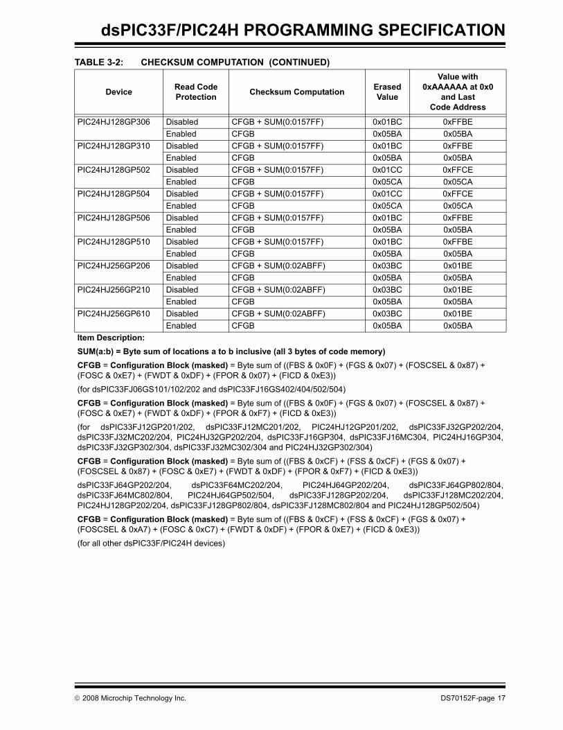
PIC24HJ128GP306 Disabled CFGB + SUM(0:0157FF) 0x01BC 0xFFBEEnabled CFGB 0x05BA 0x05BA
PIC24HJ128GP310 Disabled CFGB + SUM(0:0157FF) 0x01BC 0xFFBEEnabled CFGB 0x05BA 0x05BA
PIC24HJ128GP502 Disabled CFGB + SUM(0:0157FF) 0x01CC 0xFFCEEnabled CFGB 0x05CA 0x05CA
PIC24HJ128GP504 Disabled CFGB + SUM(0:0157FF) 0x01CC 0xFFCEEnabled CFGB 0x05CA 0x05CA
PIC24HJ128GP506 Disabled CFGB + SUM(0:0157FF) 0x01BC 0xFFBEEnabled CFGB 0x05BA 0x05BA
PIC24HJ128GP510 Disabled CFGB + SUM(0:0157FF) 0x01BC 0xFFBEEnabled CFGB 0x05BA 0x05BA
PIC24HJ256GP206 Disabled CFGB + SUM(0:02ABFF) 0x03BC 0x01BEEnabled CFGB 0x05BA 0x05BA
PIC24HJ256GP210 Disabled CFGB + SUM(0:02ABFF) 0x03BC 0x01BEEnabled CFGB 0x05BA 0x05BA
PIC24HJ256GP610 Disabled CFGB + SUM(0:02ABFF) 0x03BC 0x01BEEnabled CFGB 0x05BA 0x05BA
TABLE 3-2: CHECKSUM COMPUTATION (CONTINUED)
Device Read CodeProtection Checksum Computation Erased
Value
Value with0xAAAAAA at 0x0
and LastCode Address
Item Description:SUM(a:b) = Byte sum of locations a to b inclusive (all 3 bytes of code memory)CFGB = Configuration Block (masked) = Byte sum of ((FBS & 0x0F) + (FGS & 0x07) + (FOSCSEL & 0x87) + (FOSC & 0xE7) + (FWDT & 0xDF) + (FPOR & 0x07) + (FICD & 0xE3))
(for dsPIC33FJ06GS101/102/202 and dsPIC33FJ16GS402/404/502/504)
CFGB = Configuration Block (masked) = Byte sum of ((FBS & 0x0F) + (FGS & 0x07) + (FOSCSEL & 0x87) + (FOSC & 0xE7) + (FWDT & 0xDF) + (FPOR & 0xF7) + (FICD & 0xE3))
(for dsPIC33FJ12GP201/202, dsPIC33FJ12MC201/202, PIC24HJ12GP201/202, dsPIC33FJ32GP202/204,dsPIC33FJ32MC202/204, PIC24HJ32GP202/204, dsPIC33FJ16GP304, dsPIC33FJ16MC304, PIC24HJ16GP304,dsPIC33FJ32GP302/304, dsPIC33FJ32MC302/304 and PIC24HJ32GP302/304)
CFGB = Configuration Block (masked) = Byte sum of ((FBS & 0xCF) + (FSS & 0xCF) + (FGS & 0x07) + (FOSCSEL & 0x87) + (FOSC & 0xE7) + (FWDT & 0xDF) + (FPOR & 0xF7) + (FICD & 0xE3))
dsPIC33FJ64GP202/204, dsPIC33F64MC202/204, PIC24HJ64GP202/204, dsPIC33FJ64GP802/804,dsPIC33FJ64MC802/804, PIC24HJ64GP502/504, dsPIC33FJ128GP202/204, dsPIC33FJ128MC202/204,PIC24HJ128GP202/204, dsPIC33FJ128GP802/804, dsPIC33FJ128MC802/804 and PIC24HJ128GP502/504)
CFGB = Configuration Block (masked) = Byte sum of ((FBS & 0xCF) + (FSS & 0xCF) + (FGS & 0x07) + (FOSCSEL & 0xA7) + (FOSC & 0xC7) + (FWDT & 0xDF) + (FPOR & 0xE7) + (FICD & 0xE3))
(for all other dsPIC33F/PIC24H devices)
© 2008 Microchip Technology Inc. DS70152F-page 17
dsPIC33F/PIC24H PROGRAMMING SPECIFICATION
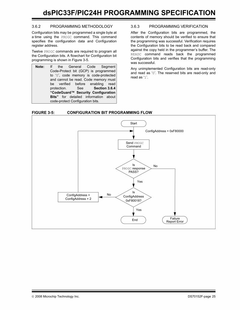
3.6 Configuration Bits Programming
3.6.1 OVERVIEWThe dsPIC33F/PIC24H devices have Configurationbits stored in twelve 8-bit Configuration registers,aligned on even configuration memory addressboundaries. These bits can be set or cleared to selectvarious device configurations. There are three types ofConfiguration bits: system operation bits, code-protectbits and unit ID bits. The system operation bitsdetermine the power-on settings for system levelcomponents, such as oscillator and Watchdog Timer.The code-protect bits prevent program memory frombeing read and written.
The register descriptions for the FBS, FSS, FGS,FOSCSEL, FOSC, FWDT, FPOR and FICDConfiguration registers are shown in Table 3-3.
The Configuration register map is shown in Table 3-4.
Note 1: If any of the code-protect bits in FBS, FSSor FGS is clear, then the entire devicemust be erased before it can bereprogrammed.
2: If user software performs an eraseoperation on the configuration fuse, itmust be followed by a write operation tothis fuse with the desired value, even ifthe desired value is the same as the stateof the erased fuse.
DS70152F-page 18 © 2008 Microchip Technology Inc.
dsPIC33F/PIC24H PROGRAMMING SPECIFICATION
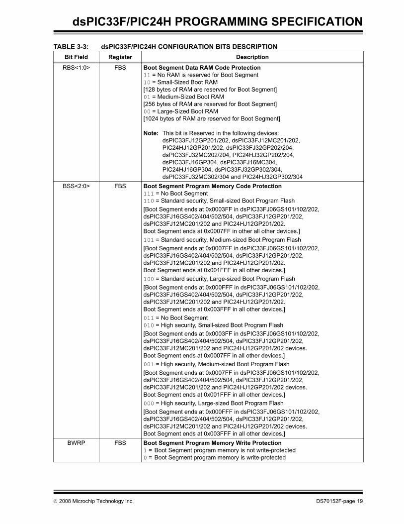
TABLE 3-3: dsPIC33F/PIC24H CONFIGURATION BITS DESCRIPTIONBit Field Register Description
RBS<1:0> FBS Boot Segment Data RAM Code Protection11 = No RAM is reserved for Boot Segment10 = Small-Sized Boot RAM[128 bytes of RAM are reserved for Boot Segment]01 = Medium-Sized Boot RAM[256 bytes of RAM are reserved for Boot Segment]00 = Large-Sized Boot RAM[1024 bytes of RAM are reserved for Boot Segment]
Note: This bit is Reserved in the following devices:dsPIC33FJ12GP201/202, dsPIC33FJ12MC201/202, PIC24HJ12GP201/202, dsPIC33FJ32GP202/204, dsPIC33FJ32MC202/204, PIC24HJ32GP202/204, dsPIC33FJ16GP304, dsPIC33FJ16MC304, PIC24HJ16GP304, dsPIC33FJ32GP302/304, dsPIC33FJ32MC302/304 and PIC24HJ32GP302/304
BSS<2:0> FBS Boot Segment Program Memory Code Protection111 = No Boot Segment110 = Standard security, Small-sized Boot Program Flash[Boot Segment ends at 0x0003FF in dsPIC33FJ06GS101/102/202, dsPIC33FJ16GS402/404/502/504, dsPIC33FJ12GP201/202, dsPIC33FJ12MC201/202 and PIC24HJ12GP201/202.Boot Segment ends at 0x0007FF in other all other devices.] 101 = Standard security, Medium-sized Boot Program Flash[Boot Segment ends at 0x0007FF in dsPIC33FJ06GS101/102/202, dsPIC33FJ16GS402/404/502/504, dsPIC33FJ12GP201/202, dsPIC33FJ12MC201/202 and PIC24HJ12GP201/202.Boot Segment ends at 0x001FFF in all other devices.] 100 = Standard security, Large-sized Boot Program Flash[Boot Segment ends at 0x000FFF in dsPIC33FJ06GS101/102/202, dsPIC33FJ16GS402/404/502/504, dsPIC33FJ12GP201/202, dsPIC33FJ12MC201/202 and PIC24HJ12GP201/202.Boot Segment ends at 0x003FFF in all other devices.] 011 = No Boot Segment010 = High security, Small-sized Boot Program Flash[Boot Segment ends at 0x0003FF in dsPIC33FJ06GS101/102/202, dsPIC33FJ16GS402/404/502/504, dsPIC33FJ12GP201/202, dsPIC33FJ12MC201/202 and PIC24HJ12GP201/202 devices.Boot Segment ends at 0x0007FF in all other devices.]001 = High security, Medium-sized Boot Program Flash[Boot Segment ends at 0x0007FF in dsPIC33FJ06GS101/102/202, dsPIC33FJ16GS402/404/502/504, dsPIC33FJ12GP201/202, dsPIC33FJ12MC201/202 and PIC24HJ12GP201/202 devices.Boot Segment ends at 0x001FFF in all other devices.]000 = High security, Large-sized Boot Program Flash[Boot Segment ends at 0x000FFF in dsPIC33FJ06GS101/102/202, dsPIC33FJ16GS402/404/502/504, dsPIC33FJ12GP201/202, dsPIC33FJ12MC201/202 and PIC24HJ12GP201/202 devices.Boot Segment ends at 0x003FFF in all other devices.]
BWRP FBS Boot Segment Program Memory Write Protection 1 = Boot Segment program memory is not write-protected0 = Boot Segment program memory is write-protected
© 2008 Microchip Technology Inc. DS70152F-page 19

dsPIC33F/PIC24H PROGRAMMING SPECIFICATION
RSS<1:0> FSS Secure Segment Data RAM Code Protection11 = No Data RAM is reserved for Secure Segment10 = Small-Sized Secure RAM [(256 - N) bytes of RAM are reserved for Secure Segment in all other devices.]01 = Medium-Sized Secure RAM[(2048 - N) bytes of RAM are reserved for Secure Segment in all other devices.]00 = Large-Sized Secure RAM [(4096 - N) bytes of RAM are reserved for Secure Segment in all other devices.] where N = Number of bytes of RAM reserved for Boot Sector.Note 1: This bit is Reserved in the following devices:
dsPIC33FJ06GS101/102/202, dsPIC33FJ16GS402/404/502/504, dsPIC33FJ12GP201/202, dsPIC33FJ12MC201/202, PIC24HJ12GP201/202, dsPIC33FJ32GP202/204, dsPIC33FJ32MC202/204, PIC24HJ32GP202/204, dsPIC33FJ16GP304, dsPIC33FJ16MC304, PIC24HJ16GP304, dsPIC33FJ32GP302/304, dsPIC33FJ32MC302/304 and PIC24HJ32GP302/304
2: If the defined Boot Segment size is greater than or equal to the defined Secure Segment, then the Secure Segment size selection has no effect and the Secure Segment is disabled.
SSS<2:0> FSS Secure Segment Program Memory Code Protection111 = No Secure Segment110 = Standard security, Small-sized Secure Program Flash [Secure Segment ends at 0x001FFF for dsPIC33FJ64GPXXX/dsPIC33FJ64MCXXX/PIC24HJ64GPXXX devices, and at 0x003FFF in other devices.]101 = Standard security, Medium-sized Secure Program Flash [Secure Segment ends at 0x003FFF for dsPIC33FJ64GPXXX/dsPIC33FJ64MCXXX/PIC24HJ64GPXXX devices, and at 0x007FFF in other devices.]100 = Standard security, Large-sized Secure Program Flash[Secure Segment ends at 0x007FFF for dsPIC33FJ64GPXXX/dsPIC33FJ64MCXXX/PIC24HJ64GPXXX devices, and at 0x00FFFF in other devices.]011 = No Secure Segment010 = High security, Small-sized Secure Program Flash [Secure Segment ends at 0x001FFF for dsPIC33FJ64GPXXX/dsPIC33FJ64MCXXX/PIC24HJ64GPXXX devices, and at 0x003FFF in other devices.]001 = High security, Medium-sized Secure Program Flash [Secure Segment ends at 0x003FFF for dsPIC33FJ64GPXXX/dsPIC33FJ64MCXXX/PIC24HJ64GPXXX devices, and at 0x007FFF in other devices.]000 = High security, Large-sized Secure Program Flash[Secure Segment ends at 0x007FFF for dsPIC33FJ64GPXXX/dsPIC33FJ64MCXXX/PIC24HJ64GPXXX devices, and at 0x00FFFF in other devices.]
Note: This bit is Reserved in the following devices:dsPIC33FJ06GS101/102/202, dsPIC33FJ16GS402/404/502/504,dsPIC33FJ12GP201/202, dsPIC33FJ12MC201/202, PIC24HJ12GP201/202, dsPIC33FJ32GP202/204, dsPIC33FJ32MC202/204, PIC24HJ32GP202/204, dsPIC33FJ16GP304, dsPIC33FJ16MC304, PIC24HJ16GP304, dsPIC33FJ32GP302/304, dsPIC33FJ32MC302/304 and PIC24HJ32GP302/304
TABLE 3-3: dsPIC33F/PIC24H CONFIGURATION BITS DESCRIPTION (CONTINUED)Bit Field Register Description
DS70152F-page 20 © 2008 Microchip Technology Inc.
dsPIC33F/PIC24H PROGRAMMING SPECIFICATION
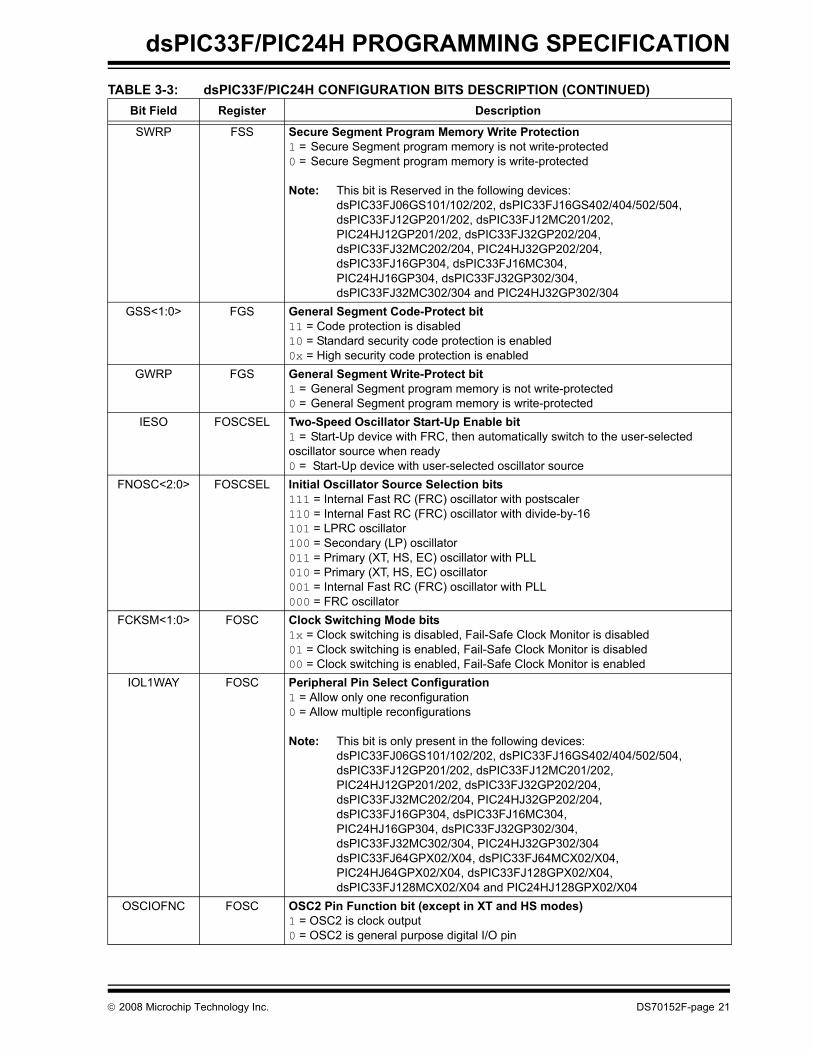
SWRP FSS Secure Segment Program Memory Write Protection 1 = Secure Segment program memory is not write-protected0 = Secure Segment program memory is write-protected
Note: This bit is Reserved in the following devices:dsPIC33FJ06GS101/102/202, dsPIC33FJ16GS402/404/502/504,dsPIC33FJ12GP201/202, dsPIC33FJ12MC201/202, PIC24HJ12GP201/202, dsPIC33FJ32GP202/204, dsPIC33FJ32MC202/204, PIC24HJ32GP202/204, dsPIC33FJ16GP304, dsPIC33FJ16MC304, PIC24HJ16GP304, dsPIC33FJ32GP302/304, dsPIC33FJ32MC302/304 and PIC24HJ32GP302/304
GSS<1:0> FGS General Segment Code-Protect bit11 = Code protection is disabled10 = Standard security code protection is enabled0x = High security code protection is enabled
GWRP FGS General Segment Write-Protect bit1 = General Segment program memory is not write-protected0 = General Segment program memory is write-protected
IESO FOSCSEL Two-Speed Oscillator Start-Up Enable bit1 = Start-Up device with FRC, then automatically switch to the user-selected oscillator source when ready0 = Start-Up device with user-selected oscillator source
FNOSC<2:0> FOSCSEL Initial Oscillator Source Selection bits111 = Internal Fast RC (FRC) oscillator with postscaler110 = Internal Fast RC (FRC) oscillator with divide-by-16101 = LPRC oscillator100 = Secondary (LP) oscillator011 = Primary (XT, HS, EC) oscillator with PLL010 = Primary (XT, HS, EC) oscillator001 = Internal Fast RC (FRC) oscillator with PLL000 = FRC oscillator
FCKSM<1:0> FOSC Clock Switching Mode bits1x = Clock switching is disabled, Fail-Safe Clock Monitor is disabled01 = Clock switching is enabled, Fail-Safe Clock Monitor is disabled00 = Clock switching is enabled, Fail-Safe Clock Monitor is enabled
IOL1WAY FOSC Peripheral Pin Select Configuration1 = Allow only one reconfiguration0 = Allow multiple reconfigurations
Note: This bit is only present in the following devices: dsPIC33FJ06GS101/102/202, dsPIC33FJ16GS402/404/502/504, dsPIC33FJ12GP201/202, dsPIC33FJ12MC201/202, PIC24HJ12GP201/202, dsPIC33FJ32GP202/204, dsPIC33FJ32MC202/204, PIC24HJ32GP202/204, dsPIC33FJ16GP304, dsPIC33FJ16MC304, PIC24HJ16GP304, dsPIC33FJ32GP302/304, dsPIC33FJ32MC302/304, PIC24HJ32GP302/304 dsPIC33FJ64GPX02/X04, dsPIC33FJ64MCX02/X04, PIC24HJ64GPX02/X04, dsPIC33FJ128GPX02/X04, dsPIC33FJ128MCX02/X04 and PIC24HJ128GPX02/X04
OSCIOFNC FOSC OSC2 Pin Function bit (except in XT and HS modes)1 = OSC2 is clock output0 = OSC2 is general purpose digital I/O pin
TABLE 3-3: dsPIC33F/PIC24H CONFIGURATION BITS DESCRIPTION (CONTINUED)Bit Field Register Description
© 2008 Microchip Technology Inc. DS70152F-page 21
dsPIC33F/PIC24H PROGRAMMING SPECIFICATION
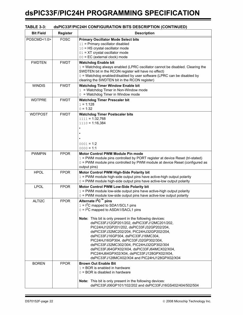
POSCMD<1:0> FOSC Primary Oscillator Mode Select bits11 = Primary oscillator disabled10 = HS crystal oscillator mode01 = XT crystal oscillator mode00 = EC (external clock) mode
FWDTEN FWDT Watchdog Enable bit1 = Watchdog always enabled (LPRC oscillator cannot be disabled. Clearing the SWDTEN bit in the RCON register will have no effect)0 = Watchdog enabled/disabled by user software (LPRC can be disabled by clearing the SWDTEN bit in the RCON register)
WINDIS FWDT Watchdog Timer Window Enable bit1 = Watchdog Timer in Non-Window mode0 = Watchdog Timer in Window mode
WDTPRE FWDT Watchdog Timer Prescaler bit1 = 1:1280 = 1:32
WDTPOST FWDT Watchdog Timer Postscaler bits1111 = 1:32,7681110 = 1:16,384•••0001 = 1:20000 = 1:1
PWMPIN FPOR Motor Control PWM Module Pin mode1 = PWM module pins controlled by PORT register at device Reset (tri-stated)0 = PWM module pins controlled by PWM module at device Reset (configured as output pins)
HPOL FPOR Motor Control PWM High-Side Polarity bit1 = PWM module high-side output pins have active-high output polarity0 = PWM module high-side output pins have active-low output polarity
LPOL FPOR Motor Control PWM Low-Side Polarity bit1 = PWM module low-side output pins have active-high output polarity0 = PWM module low-side output pins have active-low output polarity
ALTI2C FPOR Alternate I2C™ pins1 = I2C mapped to SDA1/SCL1 pins0 = I2C mapped to ASDA1/SACL1 pins
Note: This bit is only present in the following devices:dsPIC33FJ12GP201/202, dsPIC33FJ12MC201/202, PIC24HJ12GP201/202, dsPIC33FJ32GP202/204, dsPIC33FJ32MC202/204, PIC24HJ32GP202/204, dsPIC33FJ16GP304, dsPIC33FJ16MC304, PIC24HJ16GP304, dsPIC33FJ32GP302/304, dsPIC33FJ32MC302/304, PIC24HJ32GP302/304 dsPIC33FJ64GPX02/X04, dsPIC33FJ64MCX02/X04, PIC24HJ64GPX02/X04, dsPIC33FJ128GPX02/X04, dsPIC33FJ128MCX02/X04 and PIC24HJ128GPX02/X04
BOREN FPOR Brown Out Enable Bit1 = BOR is enabled in hardware0 = BOR is disabled in hardware
Note: This bit is only present in the following devices:dsPIC33FJ06GP101/102/202 and dsPIC33FJ16GS402/404/502/504
TABLE 3-3: dsPIC33F/PIC24H CONFIGURATION BITS DESCRIPTION (CONTINUED)Bit Field Register Description
DS70152F-page 22 © 2008 Microchip Technology Inc.

dsPIC33F/PIC24H PROGRAMMING SPECIFICATION
FPWRT<2:0> FPOR Power-On Reset Timer Value Select bits111 = PWRT = 128 ms110 = PWRT = 64 ms101 = PWRT = 32 ms100 = PWRT = 16 ms011 = PWRT = 8 ms010 = PWRT = 4 ms001 = PWRT = 2 ms000 = PWRT Disabled
BKBUG FICD Background Debug Enable bit1 = Device will reset in User mode0 = Device will reset in Debug mode
COE FICD Debugger/Emulator Enable bit1 = Device will reset in Operational mode0 = Device will reset in Clip-On Emulation mode
JTAGEN FICD JTAG Enable bit1 = JTAG enabled0 = JTAG disabled
ICS<1:0> FICD ICD Communication Channel Select bits11 = Communicate on PGC1/EMUC1 and PGD1/EMUD110 = Communicate on PGC2/EMUC2 and PGD2/EMUD201 = Communicate on PGC3/EMUC3 and PGD3/EMUD300 = Reserved, do not use
— All Unimplemented (read as ‘0’, write as ‘0’)
TABLE 3-3: dsPIC33F/PIC24H CONFIGURATION BITS DESCRIPTION (CONTINUED)Bit Field Register Description
© 2008 Microchip Technology Inc. DS70152F-page 23

dsPIC33F/PIC24H PROGRAMMING SPECIFICATION
TABLE 3-4: dsPIC33F/PIC24H DEVICE CONFIGURATION REGISTER MAP Address Name Bit 7 Bit 6 Bit 5 Bit 4 Bit 3 Bit 2 Bit 1 Bit 0
0xF80000 FBS RBS<1:0>(3) — BSS<2:0> BWRP0xF80002 FSS RSS<1:0>(3) — SSS<2:0>(3) SWRP(3)
0xF80004 FGS — GSS<1:0> GWRP0xF80006 FOSCSEL IESO — — — FNOSC<2:0>0xF80008 FOSC FCKSM<1:0> IOL1WAY(2) — OSCIOFNC POSCMD<1:0>0xF8000A FWDT FWDTEN WINDIS — WDTPRE WDTPOST<3:0>0xF8000C FPOR PWMPIN(1) HPOL(1) LPOL(1) ALTI2C(2) BOREN(5) FPWRT<2:0>0xF8000E FICD BKBUG COE JTAGEN(4) — ICS<1:0>0xF80010 FUID0 User Unit ID Byte 00xF80012 FUID1 User Unit ID Byte 10xF80014 FUID2 User Unit ID Byte 20xF80016 FUID3 User Unit ID Byte 3Note 1: On the dsPIC33F General Purpose Family devices (dsPIC33FJXXXGPXXX) and PIC24H devices, these
bits are reserved (read as ‘1’ and must be programmed as ‘1’).2: These bits are only present in the dsPIC33FJ12GP201/202, dsPIC33FJ12MC201/202,
PIC24HJ12GP201/202, dsPIC33FJ32GP202/204, dsPIC33FJ32MC202/204, PIC24HJ32GP202/204, dsPIC33FJ16GP304, dsPIC33FJ16MC304 and PIC24HJ16GP304 devices. In all other devices, these bits are unimplemented.
3: In the dsPIC33FJ06GS101/102/202, dsPIC33FJ16GS402/402/502/504, dsPIC33FJ12GP201/202, dsPIC33FJ12MC201/202, PIC24HJ12GP201/202, dsPIC33FJ32GP202/204, dsPIC33FJ32MC202/204, PIC24HJ32GP202/204, dsPIC33FJ16GP304, dsPIC33FJ16MC304, PIC24HJ16GP304, dsPIC33FJ32GP302/304, dsPIC33FJ32MC302/304 and PIC24HJ32GP302/304 devices, these bits are reserved.
4: The JTAGEN bit is set to ‘1’ by factory default. Microchip programmers such as ICD2 and REAL ICE clear this bit by default when connecting to a device.
5: This bit is only present in the dsPIC33FJ06GS101/102/202 and dsPIC33FJ16GS402/404/502/504 devices.
DS70152F-page 24 © 2008 Microchip Technology Inc.
dsPIC33F/PIC24H PROGRAMMING SPECIFICATION
3.6.2 PROGRAMMING METHODOLOGYConfiguration bits may be programmed a single byte ata time using the PROGC command. This commandspecifies the configuration data and Configurationregister address.
Twelve PROGC commands are required to program allthe Configuration bits. A flowchart for Configuration bitprogramming is shown in Figure 3-5.
3.6.3 PROGRAMMING VERIFICATIONAfter the Configuration bits are programmed, thecontents of memory should be verified to ensure thatthe programming was successful. Verification requiresthe Configuration bits to be read back and comparedagainst the copy held in the programmer’s buffer. TheREADC command reads back the programmedConfiguration bits and verifies that the programmingwas successful.
Any unimplemented Configuration bits are read-onlyand read as ‘0’. The reserved bits are read-only andread as ‘1’.
FIGURE 3-5: CONFIGURATION BIT PROGRAMMING FLOW
Note: If the General Code SegmentCode-Protect bit (GCP) is programmedto ‘0’, code memory is code-protectedand cannot be read. Code memory mustbe verified before enabling readprotection. See Section 3.6.4“CodeGuard™ Security ConfigurationBits” for detailed information aboutcode-protect Configuration bits.
Send PROGCCommand
ConfigAddress = 0xF80000
IsPROGC response
PASS?
No
Yes
No
FailureReport Error
Start
End
Yes
IsConfigAddress
0xF80018?
ConfigAddress =ConfigAddress + 2
© 2008 Microchip Technology Inc. DS70152F-page 25
dsPIC33F/PIC24H PROGRAMMING SPECIFICATION
3.6.4 CodeGuard™ SECURITY CONFIGURATION BITS
The FBS, FSS and FGS Configuration registers arespecial Configuration registers that control the size andlevel of code protection for the Boot Segment, SecureSegment and General Segment, respectively. For eachsegment, two main forms of code protection areprovided. One form prevents code memory from beingwritten (write protection), while the other prevents codememory from being read (read protection).
BWRP, SWRP and GWRP bits control write protectionand BSS<2:0>, SSS<2:0> and GSS<1:0> bits controlsread protection. The Chip Erase ERASEB commandsets all the code protection bits to ‘1’, which allows thedevice to be programmed.
When write protection is enabled, any programmingoperation to code memory will fail. When readprotection is enabled, any read from code memory willcause a ‘0x0’ to be read, regardless of the actualcontents of code memory. Since the programmingexecutive always verifies what it programs, attemptingto program code memory with read protection enabledwill also result in failure.
It is imperative that all code protection bits are ‘1’ whilethe device is being programmed and verified. Only afterthe device is programmed and verified should any ofthe above bits be programmed to ‘0’.
In addition to code memory protection, a part of DataRAM can be configured to be accessible only by coderesident in the Boot Segment and/or Secure Segment.The sizes of these “reserved” sections areuser-configurable, using the RBS<1:0> and RSS<1:0>bits.
3.6.5 USER UNIT IDThe dsPIC33F/PIC24H devices provide four 8-bitConfiguration registers (FUID0 through FUID3) for theuser to store product-specific information, such as unitserial numbers and other product manufacturing data.
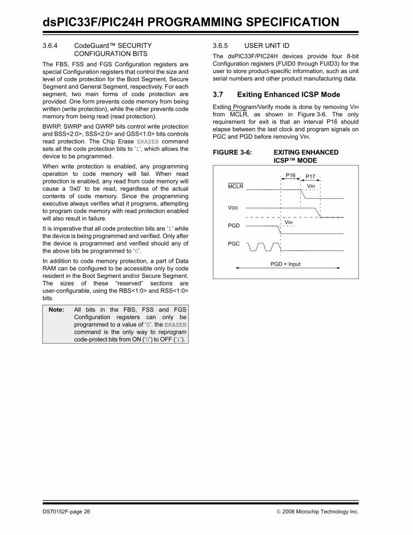
3.7 Exiting Enhanced ICSP ModeExiting Program/Verify mode is done by removing VIHfrom MCLR, as shown in Figure 3-6. The onlyrequirement for exit is that an interval P16 shouldelapse between the last clock and program signals onPGC and PGD before removing VIH.
FIGURE 3-6: EXITING ENHANCED ICSP™ MODE
Note: All bits in the FBS, FSS and FGSConfiguration registers can only beprogrammed to a value of ‘0’. the ERASEBcommand is the only way to reprogramcode-protect bits from ON (‘0’) to OFF (‘1’).
MCLR
P16
PGD
PGD = Input
PGC
VDD
VIH
VIH
P17
DS70152F-page 26 © 2008 Microchip Technology Inc.

dsPIC33F/PIC24H PROGRAMMING SPECIFICATION
4.0 THE PROGRAMMING EXECUTIVE
4.1 Programming Executive Communication
The programmer and programming executive have amaster-slave relationship, where the programmer isthe master programming device and the programmingexecutive is the slave.
All communication is initiated by the programmer in theform of a command. Only one command at a time canbe sent to the programming executive. In turn, theprogramming executive only sends one response tothe programmer after receiving and processing acommand. The programming executive command setis described in Section 4.2 “Programming ExecutiveCommands”. The response set is described inSection 4.3 “Programming Executive Responses”.
4.1.1 COMMUNICATION INTERFACE AND PROTOCOL
The ICSP/Enhanced ICSP interface is a 2 wire SPIimplemented using the PGC and PGD pins. The PGCpin is used as a clock input pin and the clock sourcemust be provided by the programmer. The PGD pin isused for sending command data to and receivingresponse data from the programming executive. Allserial data is transmitted on the falling edge of PGCand latched on the rising edge of PGC. All datatransmissions are sent to the Most Significant bit firstusing 16-bit mode (see Figure 4-1).
FIGURE 4-1: PROGRAMMING EXECUTIVE SERIAL TIMING
Since a 2 wire SPI is used, and data transmissions arebidirectional, a simple protocol is used to control thedirection of PGD. When the programmer completes acommand transmission, it releases the PGD line andallows the programming executive to drive this linehigh. The programming executive keeps the PGD linehigh to indicate that it is processing the command.
After the programming executive has processed thecommand, it brings PGD low for 15 μsec to indicate tothe programmer that the response is available to beclocked out. The programmer can begin to clock outthe response 23 μsec after PGD is brought low and itmust provide the necessary amount of clock pulses toreceive the entire response from the programmingexecutive.
After the entire response is clocked out, theprogrammer should terminate the clock on PGC until itis time to send another command to the programmingexecutive. This protocol is shown in Figure 4-2.
4.1.2 SPI RATEIn Enhanced ICSP mode, the dsPIC33F/PIC24H familydevices operate from the Fast Internal RC oscillator,which has a nominal frequency of 7.3728 MHz. Thisoscillator frequency yields an effective system clockfrequency of 1.8432 MHz. To ensure that theprogrammer does not clock too fast, it is recommendedthat a 7.35 MHz clock be provided by the programmer.
4.1.3 TIME OUTSThe programming executive uses no Watchdog or timeout for transmitting responses to the programmer. If theprogrammer does not follow the flow controlmechanism using PGC as described in Section 4.1.1“Communication Interface and Protocol”, it ispossible that the programming executive will behaveunexpectedly while trying to send a response to theprogrammer. Since the programming executive has notime out, it is imperative that the programmer correctlyfollow the described communication protocol.
As a safety measure, the programmer should use thecommand time outs identified in Table 4-1. If thecommand time out expires, the programmer shouldreset the programming executive and startprogramming the device again.
PGC
PGD
1 2 3 11 13 15 161412
LSb14 13 12 11
4 5 6
MSb 123... 45
P2
P3
P1
P1BP1A
© 2008 Microchip Technology Inc. DS70152F-page 27
dsPIC33F/PIC24H PROGRAMMING SPECIFICATION
FIGURE 4-2: PROGRAMMING EXECUTIVE – PROGRAMMER COMMUNICATION PROTOCOL
4.2 Programming Executive Commands
The programming executive command set is shown inTable 4-1. This table contains the opcode, mnemonic,length, time out and description for each command.Functional details on each command are provided inthe command descriptions (Section 4.2.4 “CommandDescriptions”).
4.2.1 COMMAND FORMATAll programming executive commands have a generalformat consisting of a 16-bit header and any requireddata for the command (see Figure 4-3). The 16-bitheader consists of a 4-bit opcode field, which is used toidentify the command, followed by a 12-bit commandlength field.
FIGURE 4-3: COMMAND FORMAT
The command opcode must match one of those in thecommand set. Any command that is received whichdoes not match the list in Table 4-1 will return a “NACK”response (see Section 4.3.1.1 “Opcode Field”).
The command length is represented in 16-bit wordssince the SPI operates in 16-bit mode. Theprogramming executive uses the command length fieldto determine the number of words to read from the SPIport. If the value of this field is incorrect, the commandwill not be properly received by the programmingexecutive.
4.2.2 PACKED DATA FORMATWhen 24-bit instruction words are transferred acrossthe 16-bit SPI interface, they are packed to conservespace using the format shown in Figure 4-4. Thisformat minimizes traffic over the SPI and provides theprogramming executive with data that is properlyaligned for performing table write operations.
FIGURE 4-4: PACKED INSTRUCTION WORD FORMAT
4.2.3 PROGRAMMING EXECUTIVE ERROR HANDLING
The programming executive will “NACK” allunsupported commands. Additionally, due to thememory constraints of the programming executive, nochecking is performed on the data contained in theprogrammer command. It is the responsibility of theprogrammer to command the programming executivewith valid command arguments or the programmingoperation may fail. Additional information on errorhandling is provided in Section 4.3.1.3 “QE_CodeField”.
1 2 15 16 1 2 15 16
PGC
PGD
PGC = Input PGC = Input (Idle)
Host TransmitsLast Command Word
PGD = Input PGD = Output
P8
1 2 15 16
MSB X X X LSB MSB X X X LSB MSB X X X LSB1 0
P9b
PGC = InputPGD = Output
P9a
Programming ExecutiveProcesses Command Host Clocks Out Response
8ns23 µs
15 12 11 0Opcode Length
Command Data First Word (if required)••
Command Data Last Word (if required)
Note: When the number of instruction wordstransferred is odd, MSB2 is zero andLSW2 can not be transmitted.
15 8 7 0LSW1
MSB2 MSB1LSW2
LSWx: Least Significant 16 bits of instruction wordMSBx: Most Significant Byte of instruction word
DS70152F-page 28 © 2008 Microchip Technology Inc.
dsPIC33F/PIC24H PROGRAMMING SPECIFICATION
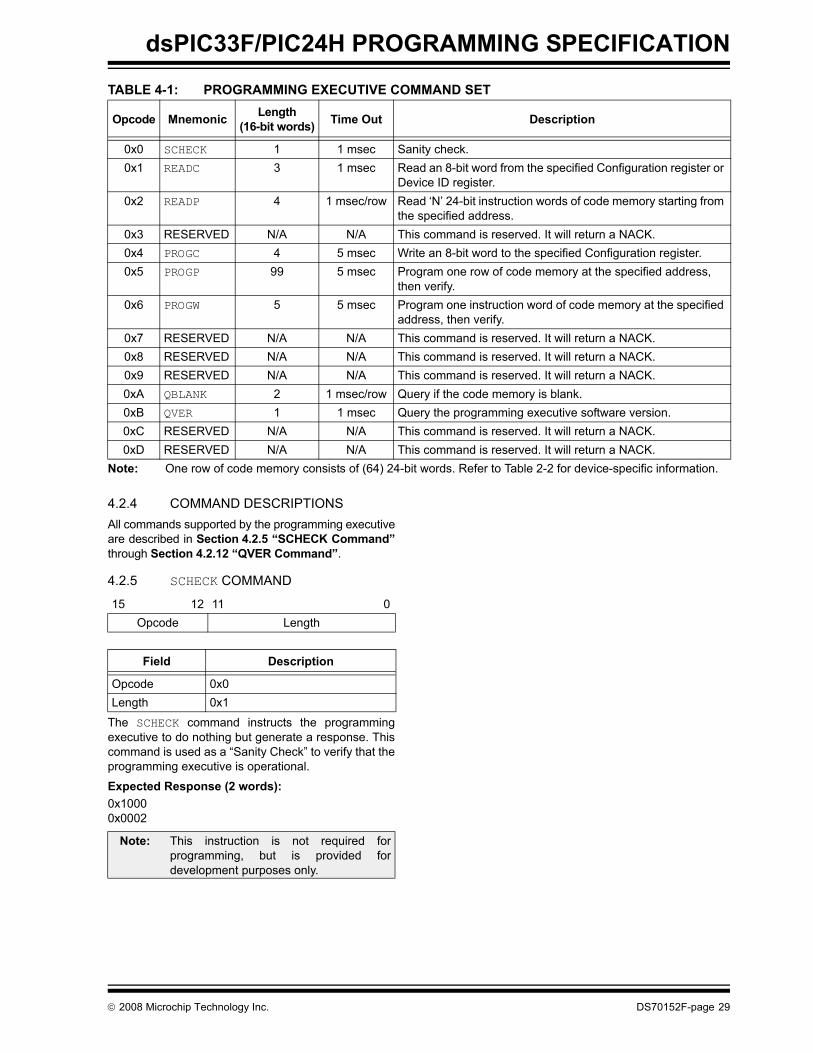
TABLE 4-1: PROGRAMMING EXECUTIVE COMMAND SET
4.2.4 COMMAND DESCRIPTIONSAll commands supported by the programming executiveare described in Section 4.2.5 “SCHECK Command”through Section 4.2.12 “QVER Command”.
4.2.5 SCHECK COMMAND
The SCHECK command instructs the programmingexecutive to do nothing but generate a response. Thiscommand is used as a “Sanity Check” to verify that theprogramming executive is operational.
Expected Response (2 words):0x10000x0002
Opcode Mnemonic Length(16-bit words) Time Out Description
0x0 SCHECK 1 1 msec Sanity check.0x1 READC 3 1 msec Read an 8-bit word from the specified Configuration register or
Device ID register.0x2 READP 4 1 msec/row Read ‘N’ 24-bit instruction words of code memory starting from
the specified address.0x3 RESERVED N/A N/A This command is reserved. It will return a NACK.0x4 PROGC 4 5 msec Write an 8-bit word to the specified Configuration register.0x5 PROGP 99 5 msec Program one row of code memory at the specified address,
then verify. 0x6 PROGW 5 5 msec Program one instruction word of code memory at the specified
address, then verify. 0x7 RESERVED N/A N/A This command is reserved. It will return a NACK.0x8 RESERVED N/A N/A This command is reserved. It will return a NACK.0x9 RESERVED N/A N/A This command is reserved. It will return a NACK.0xA QBLANK 2 1 msec/row Query if the code memory is blank.0xB QVER 1 1 msec Query the programming executive software version.0xC RESERVED N/A N/A This command is reserved. It will return a NACK.0xD RESERVED N/A N/A This command is reserved. It will return a NACK.
Note: One row of code memory consists of (64) 24-bit words. Refer to Table 2-2 for device-specific information.
15 12 11 0Opcode Length
Field Description
Opcode 0x0Length 0x1
Note: This instruction is not required forprogramming, but is provided fordevelopment purposes only.
© 2008 Microchip Technology Inc. DS70152F-page 29

dsPIC33F/PIC24H PROGRAMMING SPECIFICATION
4.2.6 READC COMMAND
The READC command instructs the programmingexecutive to read N Configuration registers or DeviceID registers, starting from the 24-bit address specifiedby Addr_MSB and Addr_LS. This command can onlybe used to read 8-bit or 16-bit data.
When this command is used to read Configurationregisters, the upper byte in every data word returned bythe programming executive is 0x00 and the lower bytecontains the Configuration register value.
Expected Response (4 + 3 * (N - 1)/2 words for N odd):0x11002 + NConfiguration register or Device ID Register 1... Configuration register or Device ID Register N
4.2.7 READP COMMAND
The READP command instructs the programmingexecutive to read N 24-bit words of code memory,starting from the 24-bit address specified by Addr_MSBand Addr_LS. This command can only be used to read24-bit data. All data returned in the response to thiscommand uses the packed data format described inSection 4.2.2 “Packed Data Format”.
Expected Response (2 + 3 * N/2 words for N even):0x12002 + 3 * N/2Least significant program memory word 1... Least significant data word N
Expected Response (4 + 3 * (N - 1)/2 words for N odd):0x12004 + 3 * (N - 1)/2Least significant program memory word 1... MSB of program memory word N (zero padded)
15 12 11 8 7 0Opcode Length
N Addr_MSBAddr_LS
Field Description
Opcode 0x1Length 0x3N Number of 8-bit Configuration registers
or Device ID registers to read (maximum of 256).
Addr_MSB MSB of 24-bit source address.Addr_LS Least Significant 16 bits of 24-bit
source address.
Note: Reading unimplemented memory willcause the programming executive toreset. Please ensure that only memorylocations present on a particular deviceare accessed.
15 12 11 8 7 0Opcode Length
NReserved Addr_MSB
Addr_LS
Field Description
Opcode 0x2Length 0x4N Number of 24-bit instructions to read
(maximum of 32768).Reserved 0x0Addr_MSB MSB of 24-bit source address.Addr_LS Least Significant 16 bits of 24-bit
source address.
Note: Reading unimplemented memory willcause the programming executive toreset. Please ensure that only memorylocations present on a particular deviceare accessed.
DS70152F-page 30 © 2008 Microchip Technology Inc.

dsPIC33F/PIC24H PROGRAMMING SPECIFICATION
4.2.8 PROGC COMMAND
The PROGC command instructs the programmingexecutive to program a single Configuration register,located at the specified memory address.
After the specified data word has been programmed tocode memory, the programming executive verifies theprogrammed data against the data in the command.
Expected Response (2 words):0x14000x0002
4.2.9 PROGP COMMAND
The PROGP command instructs the programmingexecutive to program one row of code memory(64 instruction words) to the specified memoryaddress. Programming begins with the row addressspecified in the command. The destination addressshould be a multiple of 0x80.
The data to program the memory, located in commandwords D_1 through D_96, must be arranged using thepacked instruction word format shown in Figure 4-4.
After all data has been programmed to code memory,the programming executive verifies the programmeddata against the data in the command.
Expected Response (2 words):0x15000x0002
15 12 11 8 7 0Opcode Length
Reserved Addr_MSBAddr_LS
Data
Field Description
Opcode 0x4Length 0x4Reserved 0x0Addr_MSB MSB of 24-bit destination address.Addr_LS Least Significant 16 bits of 24-bit
destination address.Data 8-bit data word.
15 12 11 8 7 0Opcode Length
Reserved Addr_MSBAddr_LS
D_1D_2...
D_N
Field Description
Opcode 0x5Length 0x63Reserved 0x0Addr_MSB MSB of 24-bit destination address.Addr_LS Least Significant 16 bits of 24-bit
destination address.D_1 16-bit data word 1.D_2 16-bit data word 2.... 16-bit data word 3 through 95.D_96 16-bit data word 96.
Note: Refer to Table 2-2 for code memory sizeinformation.
© 2008 Microchip Technology Inc. DS70152F-page 31
dsPIC33F/PIC24H PROGRAMMING SPECIFICATION
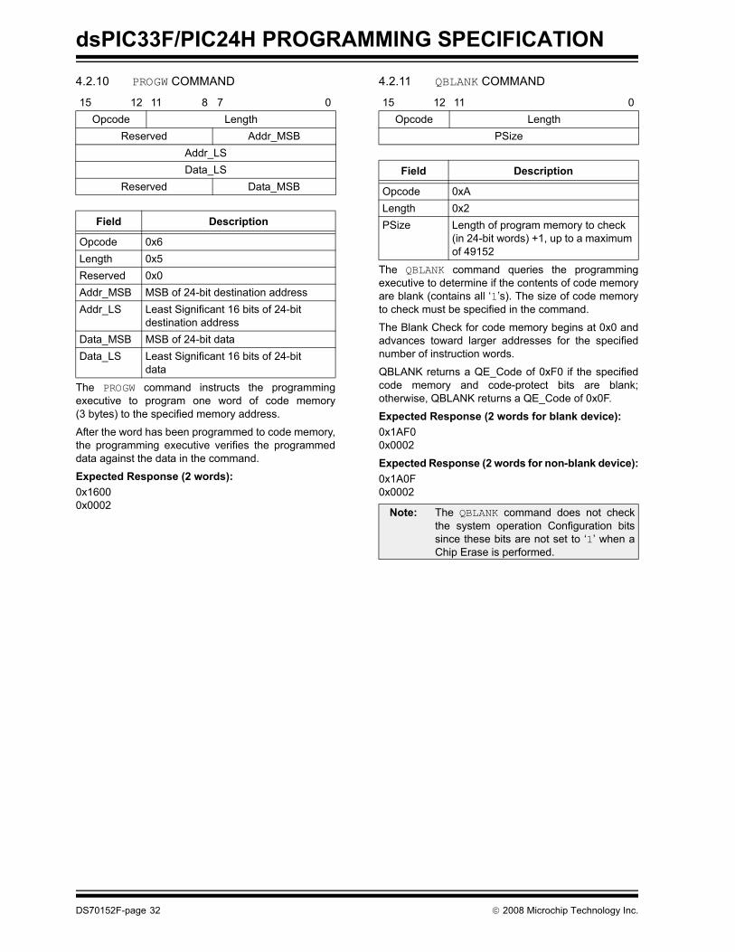
4.2.10 PROGW COMMAND
The PROGW command instructs the programmingexecutive to program one word of code memory(3 bytes) to the specified memory address.
After the word has been programmed to code memory,the programming executive verifies the programmeddata against the data in the command.
Expected Response (2 words):0x16000x0002
4.2.11 QBLANK COMMAND
The QBLANK command queries the programmingexecutive to determine if the contents of code memoryare blank (contains all ‘1’s). The size of code memoryto check must be specified in the command.
The Blank Check for code memory begins at 0x0 andadvances toward larger addresses for the specifiednumber of instruction words.
QBLANK returns a QE_Code of 0xF0 if the specifiedcode memory and code-protect bits are blank;otherwise, QBLANK returns a QE_Code of 0x0F.
Expected Response (2 words for blank device):0x1AF00x0002
Expected Response (2 words for non-blank device):0x1A0F0x0002
15 12 11 8 7 0Opcode Length
Reserved Addr_MSBAddr_LSData_LS
Reserved Data_MSB
Field Description
Opcode 0x6Length 0x5Reserved 0x0Addr_MSB MSB of 24-bit destination addressAddr_LS Least Significant 16 bits of 24-bit
destination addressData_MSB MSB of 24-bit dataData_LS Least Significant 16 bits of 24-bit
data
15 12 11 0Opcode Length
PSize
Field Description
Opcode 0xALength 0x2PSize Length of program memory to check
(in 24-bit words) +1, up to a maximum of 49152
Note: The QBLANK command does not checkthe system operation Configuration bitssince these bits are not set to ‘1’ when aChip Erase is performed.
DS70152F-page 32 © 2008 Microchip Technology Inc.
dsPIC33F/PIC24H PROGRAMMING SPECIFICATION
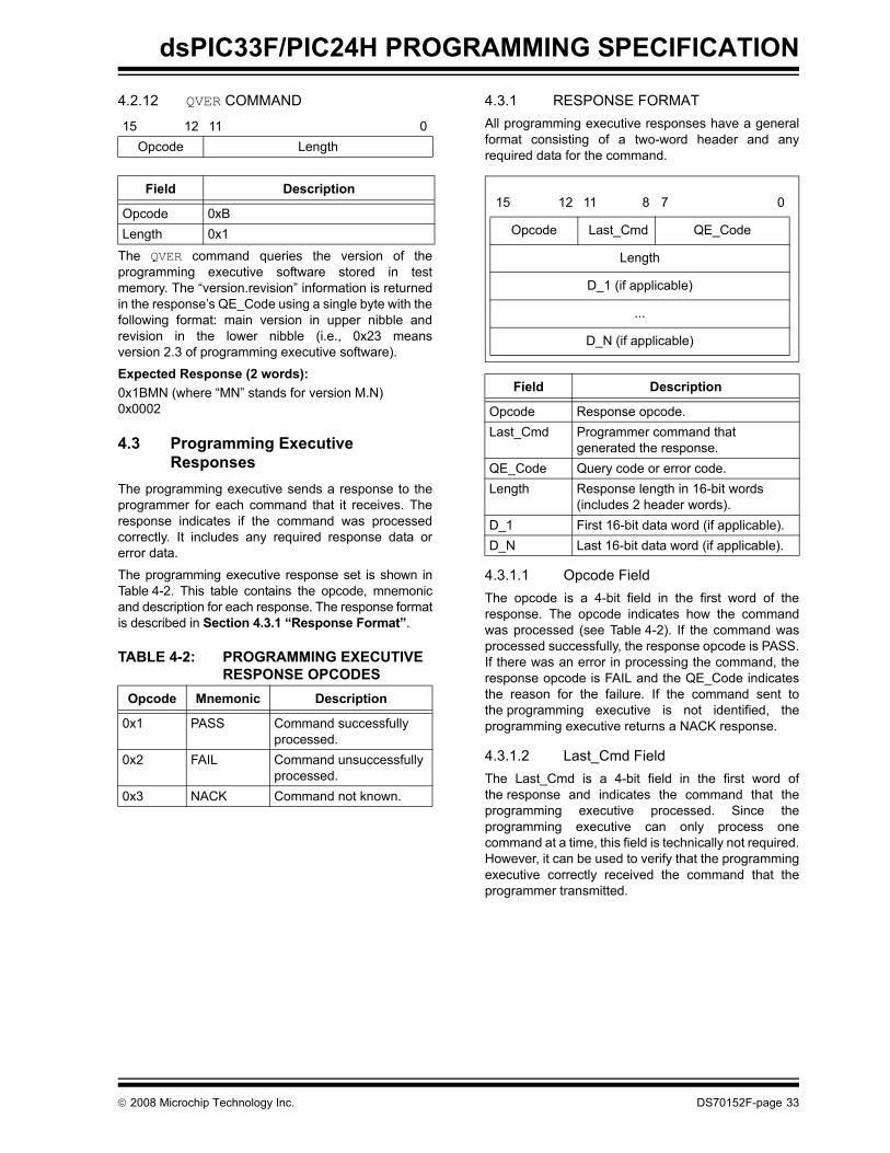
4.2.12 QVER COMMAND
The QVER command queries the version of theprogramming executive software stored in testmemory. The “version.revision” information is returnedin the response’s QE_Code using a single byte with thefollowing format: main version in upper nibble andrevision in the lower nibble (i.e., 0x23 meansversion 2.3 of programming executive software).
Expected Response (2 words):0x1BMN (where “MN” stands for version M.N)0x0002
4.3 Programming Executive Responses
The programming executive sends a response to theprogrammer for each command that it receives. Theresponse indicates if the command was processedcorrectly. It includes any required response data orerror data.
The programming executive response set is shown inTable 4-2. This table contains the opcode, mnemonicand description for each response. The response formatis described in Section 4.3.1 “Response Format”.
TABLE 4-2: PROGRAMMING EXECUTIVE RESPONSE OPCODES
4.3.1 RESPONSE FORMATAll programming executive responses have a generalformat consisting of a two-word header and anyrequired data for the command.
4.3.1.1 Opcode FieldThe opcode is a 4-bit field in the first word of theresponse. The opcode indicates how the commandwas processed (see Table 4-2). If the command wasprocessed successfully, the response opcode is PASS.If there was an error in processing the command, theresponse opcode is FAIL and the QE_Code indicatesthe reason for the failure. If the command sent tothe programming executive is not identified, theprogramming executive returns a NACK response.
4.3.1.2 Last_Cmd FieldThe Last_Cmd is a 4-bit field in the first word ofthe response and indicates the command that theprogramming executive processed. Since theprogramming executive can only process onecommand at a time, this field is technically not required.However, it can be used to verify that the programmingexecutive correctly received the command that theprogrammer transmitted.
15 12 11 0Opcode Length
Field Description
Opcode 0xBLength 0x1
Opcode Mnemonic Description
0x1 PASS Command successfully processed.
0x2 FAIL Command unsuccessfully processed.
0x3 NACK Command not known.
Field Description
Opcode Response opcode.Last_Cmd Programmer command that
generated the response.QE_Code Query code or error code.Length Response length in 16-bit words
(includes 2 header words).D_1 First 16-bit data word (if applicable).D_N Last 16-bit data word (if applicable).
15 12 11 8 7 0
Opcode Last_Cmd QE_Code
Length
D_1 (if applicable)
...
D_N (if applicable)
© 2008 Microchip Technology Inc. DS70152F-page 33
dsPIC33F/PIC24H PROGRAMMING SPECIFICATION
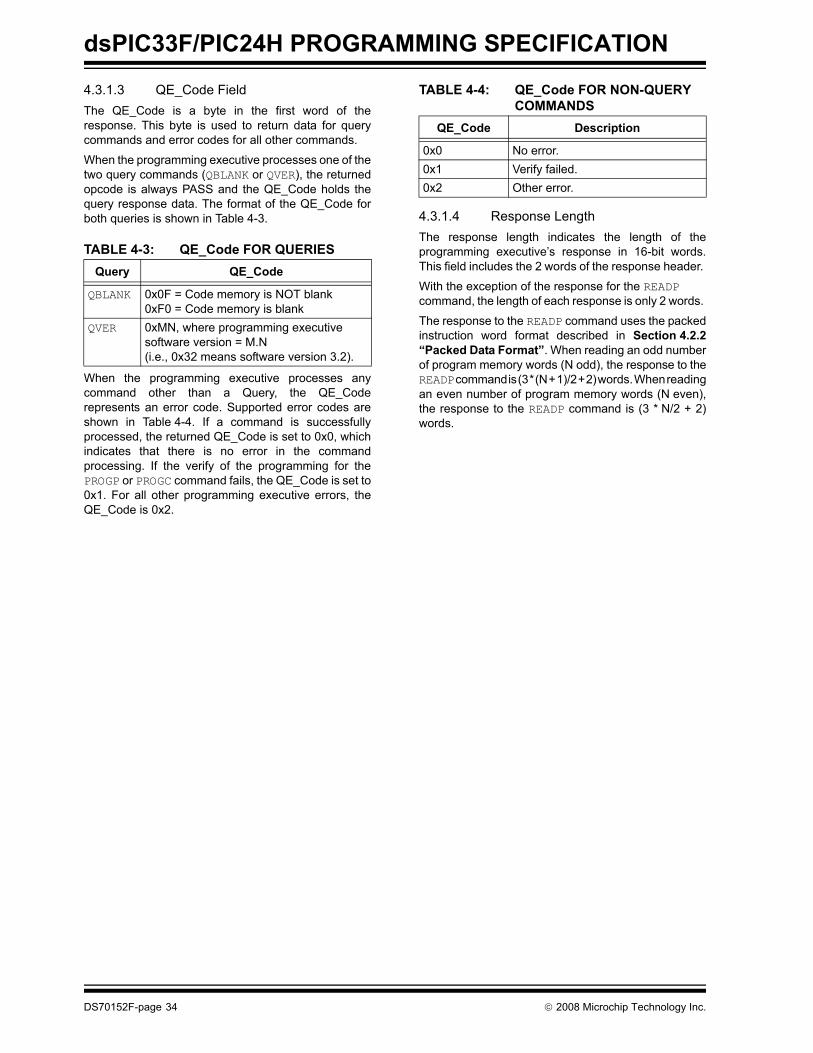
4.3.1.3 QE_Code FieldThe QE_Code is a byte in the first word of theresponse. This byte is used to return data for querycommands and error codes for all other commands.
When the programming executive processes one of thetwo query commands (QBLANK or QVER), the returnedopcode is always PASS and the QE_Code holds thequery response data. The format of the QE_Code forboth queries is shown in Table 4-3.
TABLE 4-3: QE_Code FOR QUERIES
When the programming executive processes anycommand other than a Query, the QE_Coderepresents an error code. Supported error codes areshown in Table 4-4. If a command is successfullyprocessed, the returned QE_Code is set to 0x0, whichindicates that there is no error in the commandprocessing. If the verify of the programming for thePROGP or PROGC command fails, the QE_Code is set to0x1. For all other programming executive errors, theQE_Code is 0x2.
TABLE 4-4: QE_Code FOR NON-QUERY COMMANDS
4.3.1.4 Response LengthThe response length indicates the length of theprogramming executive’s response in 16-bit words.This field includes the 2 words of the response header.
With the exception of the response for the READP command, the length of each response is only 2 words.
The response to the READP command uses the packedinstruction word format described in Section 4.2.2“Packed Data Format”. When reading an odd numberof program memory words (N odd), the response to theREADP command is (3 * (N + 1)/2 + 2) words. When readingan even number of program memory words (N even),the response to the READP command is (3 * N/2 + 2)words.
Query QE_Code
QBLANK 0x0F = Code memory is NOT blank0xF0 = Code memory is blank
QVER 0xMN, where programming executive software version = M.N(i.e., 0x32 means software version 3.2).
QE_Code Description
0x0 No error. 0x1 Verify failed.0x2 Other error.
DS70152F-page 34 © 2008 Microchip Technology Inc.
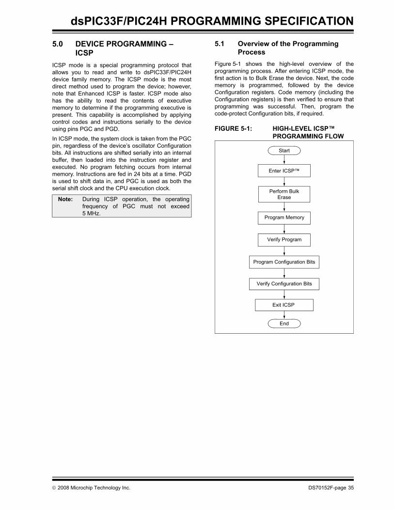
dsPIC33F/PIC24H PROGRAMMING SPECIFICATION
5.0 DEVICE PROGRAMMING – ICSP
ICSP mode is a special programming protocol thatallows you to read and write to dsPIC33F/PIC24Hdevice family memory. The ICSP mode is the mostdirect method used to program the device; however,note that Enhanced ICSP is faster. ICSP mode alsohas the ability to read the contents of executivememory to determine if the programming executive ispresent. This capability is accomplished by applyingcontrol codes and instructions serially to the deviceusing pins PGC and PGD.
In ICSP mode, the system clock is taken from the PGCpin, regardless of the device’s oscillator Configurationbits. All instructions are shifted serially into an internalbuffer, then loaded into the instruction register andexecuted. No program fetching occurs from internalmemory. Instructions are fed in 24 bits at a time. PGDis used to shift data in, and PGC is used as both theserial shift clock and the CPU execution clock.
5.1 Overview of the Programming Process
Figure 5-1 shows the high-level overview of theprogramming process. After entering ICSP mode, thefirst action is to Bulk Erase the device. Next, the codememory is programmed, followed by the deviceConfiguration registers. Code memory (including theConfiguration registers) is then verified to ensure thatprogramming was successful. Then, program thecode-protect Configuration bits, if required.
FIGURE 5-1: HIGH-LEVEL ICSP™ PROGRAMMING FLOW
Note: During ICSP operation, the operatingfrequency of PGC must not exceed5 MHz.
Start
Perform BulkErase
Program Memory
Verify Program
End
Enter ICSP™
Program Configuration Bits
Verify Configuration Bits
Exit ICSP
© 2008 Microchip Technology Inc. DS70152F-page 35
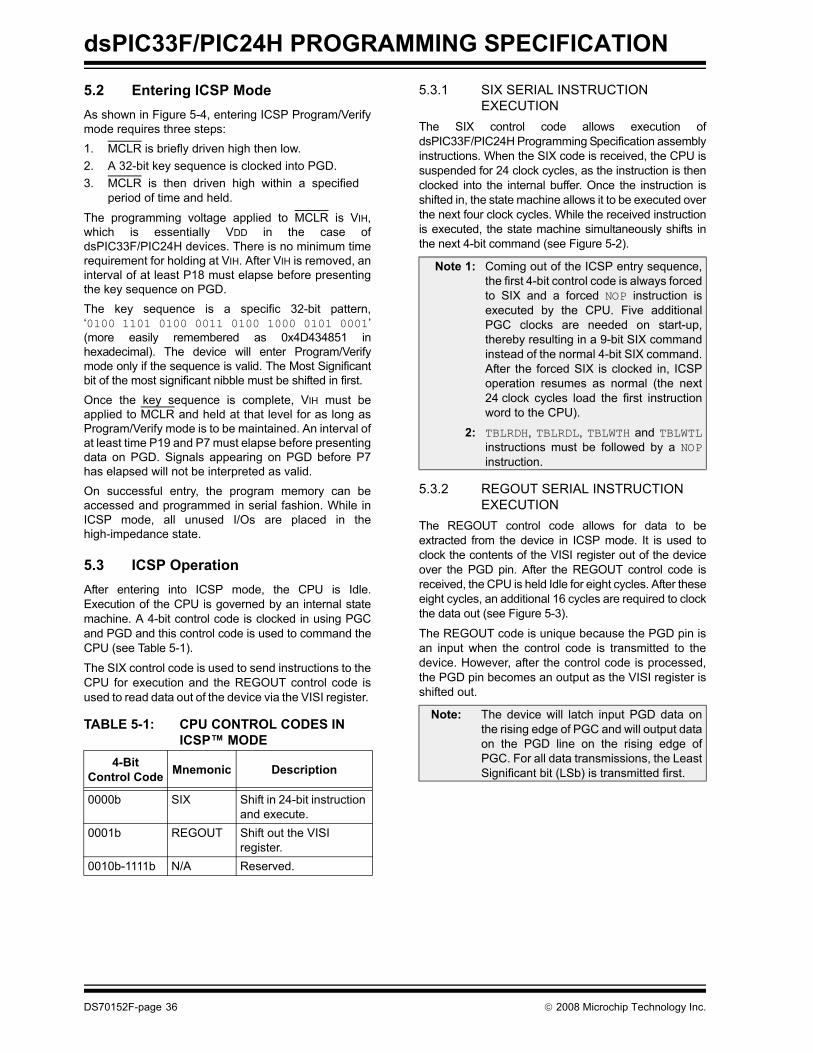
dsPIC33F/PIC24H PROGRAMMING SPECIFICATION
5.2 Entering ICSP ModeAs shown in Figure 5-4, entering ICSP Program/Verifymode requires three steps:1. MCLR is briefly driven high then low.2. A 32-bit key sequence is clocked into PGD.3. MCLR is then driven high within a specified
period of time and held.
The programming voltage applied to MCLR is VIH,which is essentially VDD in the case ofdsPIC33F/PIC24H devices. There is no minimum timerequirement for holding at VIH. After VIH is removed, aninterval of at least P18 must elapse before presentingthe key sequence on PGD.The key sequence is a specific 32-bit pattern,‘0100 1101 0100 0011 0100 1000 0101 0001’(more easily remembered as 0x4D434851 inhexadecimal). The device will enter Program/Verifymode only if the sequence is valid. The Most Significantbit of the most significant nibble must be shifted in first. Once the key sequence is complete, VIH must beapplied to MCLR and held at that level for as long asProgram/Verify mode is to be maintained. An interval ofat least time P19 and P7 must elapse before presentingdata on PGD. Signals appearing on PGD before P7has elapsed will not be interpreted as valid.On successful entry, the program memory can beaccessed and programmed in serial fashion. While inICSP mode, all unused I/Os are placed in thehigh-impedance state.
5.3 ICSP OperationAfter entering into ICSP mode, the CPU is Idle.Execution of the CPU is governed by an internal statemachine. A 4-bit control code is clocked in using PGCand PGD and this control code is used to command theCPU (see Table 5-1).
The SIX control code is used to send instructions to theCPU for execution and the REGOUT control code isused to read data out of the device via the VISI register.
TABLE 5-1: CPU CONTROL CODES IN ICSP™ MODE
5.3.1 SIX SERIAL INSTRUCTION EXECUTION
The SIX control code allows execution ofdsPIC33F/PIC24H Programming Specification assemblyinstructions. When the SIX code is received, the CPU issuspended for 24 clock cycles, as the instruction is thenclocked into the internal buffer. Once the instruction isshifted in, the state machine allows it to be executed overthe next four clock cycles. While the received instructionis executed, the state machine simultaneously shifts inthe next 4-bit command (see Figure 5-2).
5.3.2 REGOUT SERIAL INSTRUCTION EXECUTION
The REGOUT control code allows for data to beextracted from the device in ICSP mode. It is used toclock the contents of the VISI register out of the deviceover the PGD pin. After the REGOUT control code isreceived, the CPU is held Idle for eight cycles. After theseeight cycles, an additional 16 cycles are required to clockthe data out (see Figure 5-3).
The REGOUT code is unique because the PGD pin isan input when the control code is transmitted to thedevice. However, after the control code is processed,the PGD pin becomes an output as the VISI register isshifted out.
4-Bit Control Code Mnemonic Description
0000b SIX Shift in 24-bit instruction and execute.
0001b REGOUT Shift out the VISIregister.
0010b-1111b N/A Reserved.
Note 1: Coming out of the ICSP entry sequence,the first 4-bit control code is always forcedto SIX and a forced NOP instruction isexecuted by the CPU. Five additionalPGC clocks are needed on start-up,thereby resulting in a 9-bit SIX commandinstead of the normal 4-bit SIX command.After the forced SIX is clocked in, ICSPoperation resumes as normal (the next24 clock cycles load the first instructionword to the CPU).
2: TBLRDH, TBLRDL, TBLWTH and TBLWTLinstructions must be followed by a NOPinstruction.
Note: The device will latch input PGD data onthe rising edge of PGC and will output dataon the PGD line on the rising edge ofPGC. For all data transmissions, the LeastSignificant bit (LSb) is transmitted first.
DS70152F-page 36 © 2008 Microchip Technology Inc.
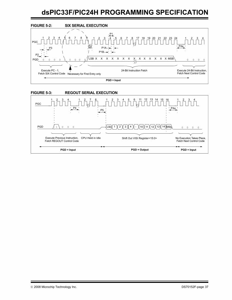
dsPIC33F/PIC24H PROGRAMMING SPECIFICATION
FIGURE 5-2: SIX SERIAL EXECUTION
FIGURE 5-3: REGOUT SERIAL EXECUTION
P4
2 3 1 2 3 23 24 1 2 3 4P1
PGCP4a
PGD
24-Bit Instruction Fetch Execute 24-Bit Instruction,Execute PC - 1,
1 4
0 0 0 0
Fetch SIX Control Code Fetch Next Control Code
4 5 6 7 8 18 19 20 21 2217
LSB X X X X X X X X X X X X X X MSB
PGD = Input
P2
P3P1B
P1A
5 6 7
0 0 0 00 0 0
Necessary for First Entry only
8 9
0 0
1 2 3 4 1 2 7 8PGC
P4
PGD
PGD = Input
Execute Previous Instruction, CPU Held in Idle Shift Out VISI Register<15:0>
P5
PGD = Output
1 2 3 1 2 3 4
P4a
11 13 15 161412
No Execution Takes Place,Fetch Next Control Code
0 0 0 0 0
PGD = Input
MSb1 2 3 41
4 5 6
LSb 141312... 11100
Fetch REGOUT Control Code
0
© 2008 Microchip Technology Inc. DS70152F-page 37
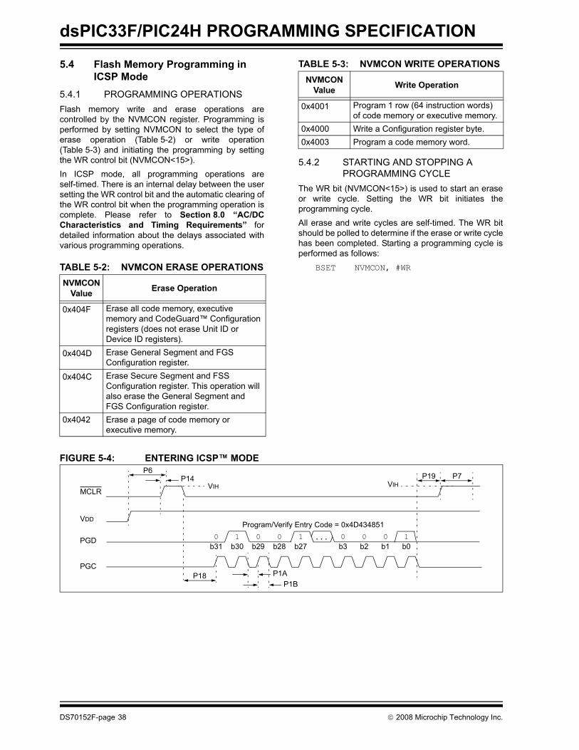
dsPIC33F/PIC24H PROGRAMMING SPECIFICATION
5.4 Flash Memory Programming in ICSP Mode
5.4.1 PROGRAMMING OPERATIONSFlash memory write and erase operations arecontrolled by the NVMCON register. Programming isperformed by setting NVMCON to select the type oferase operation (Table 5-2) or write operation(Table 5-3) and initiating the programming by settingthe WR control bit (NVMCON<15>). In ICSP mode, all programming operations areself-timed. There is an internal delay between the usersetting the WR control bit and the automatic clearing ofthe WR control bit when the programming operation iscomplete. Please refer to Section 8.0 “AC/DCCharacteristics and Timing Requirements” fordetailed information about the delays associated withvarious programming operations.
TABLE 5-2: NVMCON ERASE OPERATIONS
TABLE 5-3: NVMCON WRITE OPERATIONS
5.4.2 STARTING AND STOPPING A PROGRAMMING CYCLE
The WR bit (NVMCON<15>) is used to start an eraseor write cycle. Setting the WR bit initiates theprogramming cycle.All erase and write cycles are self-timed. The WR bitshould be polled to determine if the erase or write cyclehas been completed. Starting a programming cycle isperformed as follows:
BSET NVMCON, #WR
FIGURE 5-4: ENTERING ICSP™ MODE
NVMCONValue Erase Operation
0x404F Erase all code memory, executive memory and CodeGuard™ Configuration registers (does not erase Unit ID or Device ID registers).
0x404D Erase General Segment and FGS Configuration register.
0x404C Erase Secure Segment and FSS Configuration register. This operation will also erase the General Segment and FGS Configuration register.
0x4042 Erase a page of code memory or executive memory.
NVMCONValue Write Operation
0x4001 Program 1 row (64 instruction words) of code memory or executive memory.
0x4000 Write a Configuration register byte.0x4003 Program a code memory word.
MCLR
PGD
PGC
VDD
P6P14
b31 b30 b29 b28 b27 b2 b1 b0b3...
Program/Verify Entry Code = 0x4D434851
P1AP1B
P18
P19
0 1 0 0 1 0 0 0 1
P7VIH VIH
DS70152F-page 38 © 2008 Microchip Technology Inc.

dsPIC33F/PIC24H PROGRAMMING SPECIFICATION
REGISTER 5-1: NVMCON: FLASH MEMORY CONTROL REGISTER
R/SO-0(1) R/W-0(1) R/W-0(1) U-0 U-0 U-0 U-0 U-0WR WREN WRERR — — — — —
bit 15 bit 8
U-0 R/W-0(1) U-0 U-0 R/W-0(1) R/W-0(1) R/W-0(1) R/W-0(1)
— ERASE — — NVMOP<3:0>(2)
bit 7 bit 0
Legend: SO = Satiable only bitR = Readable bit W = Writable bit U = Unimplemented bit, read as ‘0’-n = Value at POR ‘1’ = Bit is set ‘0’ = Bit is cleared x = Bit is unknown
bit 15 WR: Write Control bit1 = Initiates a Flash memory program or erase operation. The operation is self-timed and the bit is
cleared by hardware once operation is complete0 = Program or erase operation is complete and inactive
bit 14 WREN: Write Enable bit1 = Enable Flash program/erase operations0 = Inhibit Flash program/erase operations
bit 13 WRERR: Write Sequence Error Flag bit1 = An improper program or erase sequence attempt or termination has occurred (bit is set
automatically on any set attempt of the WR bit)0 = The program or erase operation completed normally
bit 12-7 Unimplemented: Read as ‘0’bit 6 ERASE: Erase/Program Enable bit
1 = Perform the erase operation specified by NVMOP<3:0> on the next WR command0 = Perform the program operation specified by NVMOP<3:0> on the next WR command
bit 5-4 Unimplemented: Read as ‘0’bit 3-0 NVMOP<3:0>: NVM Operation Select bits(2)
If ERASE = 1:1111 = Memory bulk erase operation1110 = Reserved1101 = Erase General Segment1100 = Erase Secure Segment1011 = Reserved0011 = No operation0010 = Memory page erase operation0001 = No operation0000 = Erase a single Configuration register byte
If ERASE = 0:1111 = No operation1110 = Reserved1101 = No operation1100 = No operation1011 = Reserved0011 = Memory word program operation0010 = No operation0001 = Memory row program operation0000 = Program a single Configuration register byte
Note 1: These bits can only be reset on POR.
2: All other combinations of NVMOP<3:0> are unimplemented.
© 2008 Microchip Technology Inc. DS70152F-page 39

dsPIC33F/PIC24H PROGRAMMING SPECIFICATION
5.5 Erasing Program MemoryThe procedure for erasing program memory (all of codememory, data memory, executive memory andcode-protect bits) consists of setting NVMCON to0x404F and then executing the programming cycle. Forsegment erase operations, the NVMCON value shouldbe modified suitably, according to Table 5-2.
Figure 5-5 shows the ICSP programming process forBulk Erasing program memory. This process includesthe ICSP command code, which must be transmitted(for each instruction) Least Significant bit first, using thePGC and PGD pins (see Figure 5-2).
FIGURE 5-5: BULK ERASE FLOW
If a Segment Erase operation is required, Step 3 mustbe modified with the appropriate NVMCON value asper Table 5-2.
The ability to individually erase various segments is acritical component of the CodeGuard™ Securityfeatures on dsPIC33F/PIC24H devices. An individualcode segment may be erased without affecting othersegments. In addition, the Configuration registercorresponding to the erased code segment also getserased. For example, the user may want to erase thecode in the General Segment without erasinga bootloader located in the Boot Segment.
The Secure Segment Erase command is used to erasethe Secure Segment and the FSS Configurationregister. The General Segment Erase command isused to erase the General Segment and the FGS
Configuration register. This command is only effectiveif a Boot Segment or Secure Segment has beenenabled.
Before performing any segment erase operation, theprogrammer must first determine if thedsPIC33F/PIC24H device has defined a Boot Segmentor Secure Segment, and ensure that a segment doesnot get overwritten by operations on any othersegment. Also, a Bulk Erase should not be performedif a Boot Segment or Secure Segment has beendefined.
The BSS bit field in the FBS configuration register canbe read to determine whether a Boot Segment hasbeen defined. If a Boot Segment has already beendefined (and probably already been programmed), theuser must be warned about this fact. Similarly, the SSSbit field in the FSS configuration register can be read todetermine whether a Secure Segment has beendefined. If a Secure Segment has already been defined(and probably already been programmed), the usermust be warned about this fact.
A Bulk Erase operation is the recommendedmechanism to allow a user to overwrite the BootSegment (if one chooses to do so).
In general, the segments and CodeGuardSecurity-related configuration registers should beprogrammed in the following order:
• FBS and Boot Segment• FSS and Secure Segment• FGS and General Segment
Note: Program memory must be erased beforewriting any data to program memory.
Start
End
Set the WR bit to Initiate Erase
Write 0x404F to NVMCON SFR
Delay P11 + P10 Time
Note 1: The Boot Segment and FBSConfiguration register can only be erasedusing a Bulk Erase.
2: A Secure Segment Erase operation alsoerases the General Segment and FGSConfiguration register. This is true even ifSecure Segment is present on a devicebut not enabled.
DS70152F-page 40 © 2008 Microchip Technology Inc.

dsPIC33F/PIC24H PROGRAMMING SPECIFICATION
TABLE 5-4: SERIAL INSTRUCTION EXECUTION FOR BULK ERASING CODE MEMORY
5.6 Writing Code MemoryThe procedure for writing code memory is similar to theprocedure for writing the Configuration registers,except that 64 instruction words are programmed at atime. To facilitate this operation, working registers,W0:W5, are used as temporary holding registers for thedata to be programmed.
Table 5-5 shows the ICSP programming details,including the serial pattern with the ICSP commandcode, which must be transmitted Least Significant bitfirst using the PGC and PGD pins (see Figure 5-2). InStep 1, the Reset vector is exited. In Step 2, theNVMCON register is initialized for programming ofcode memory. In Step 3, the 24-bit starting destinationaddress for programming is loaded into the TBLPAGregister and W7 register. The upper byte of thestarting destination address is stored in TBLPAG andthe lower 16 bits of the destination address are storedin W7.
To minimize the programming time, the same packedinstruction format that the programming executive usesis utilized (Figure 4-4). In Step 4, four packedinstruction words are stored in working registers,W0:W5, using the MOV instruction and the read pointer,W6, is initialized. The contents of W0:W5 holding thepacked instruction word data are shown in Figure 5-6.In Step 5, eight TBLWT instructions are used to copy thedata from W0:W5 to the write latches of code memory.Since code memory is programmed 64 instructionwords at a time, Steps 4 and 5 are repeated 16 times toload all the write latches (Step 6).
After the write latches are loaded, programming isinitiated by writing to the NVMCON register in Steps 7and 8. In Step 9, the internal PC is reset to 0x200. This is
a precautionary measure to prevent the PC fromincrementing into unimplemented memory when largedevices are being programmed. Lastly, in Step 10,Steps 3-9 are repeated until all of code memory isprogrammed.
FIGURE 5-6: PACKED INSTRUCTION WORDS IN W0:W5
Command(Binary)
Data(Hex) Description
Step 1: Exit the Reset vector.000000000000
040200040200000000
GOTO 0x200GOTO 0x200NOP
Step 2: Set the NVMCON to erase all program memory.00000000
2404FA883B0A
MOV #0x404F, W10MOV W10, NVMCON
Step 3: Initiate the erase cycle.00000000000000000000
A8E761000000000000000000000000
BSET NVMCON, #WR NOPNOPNOPNOP
Step 4: Wait for Bulk Erase operation to complete and make sure WR bit is clear.— — Externally time ‘P11’ msec (see Section 8.0 “AC/DC Characteristics and
Timing Requirements”) to allow sufficient time for the Bulk Erase operation to complete.
15 8 7 0
W0 LSW0W1 MSB1 MSB0W2 LSW1W3 LSW2W4 MSB3 MSB2W5 LSW3
© 2008 Microchip Technology Inc. DS70152F-page 41
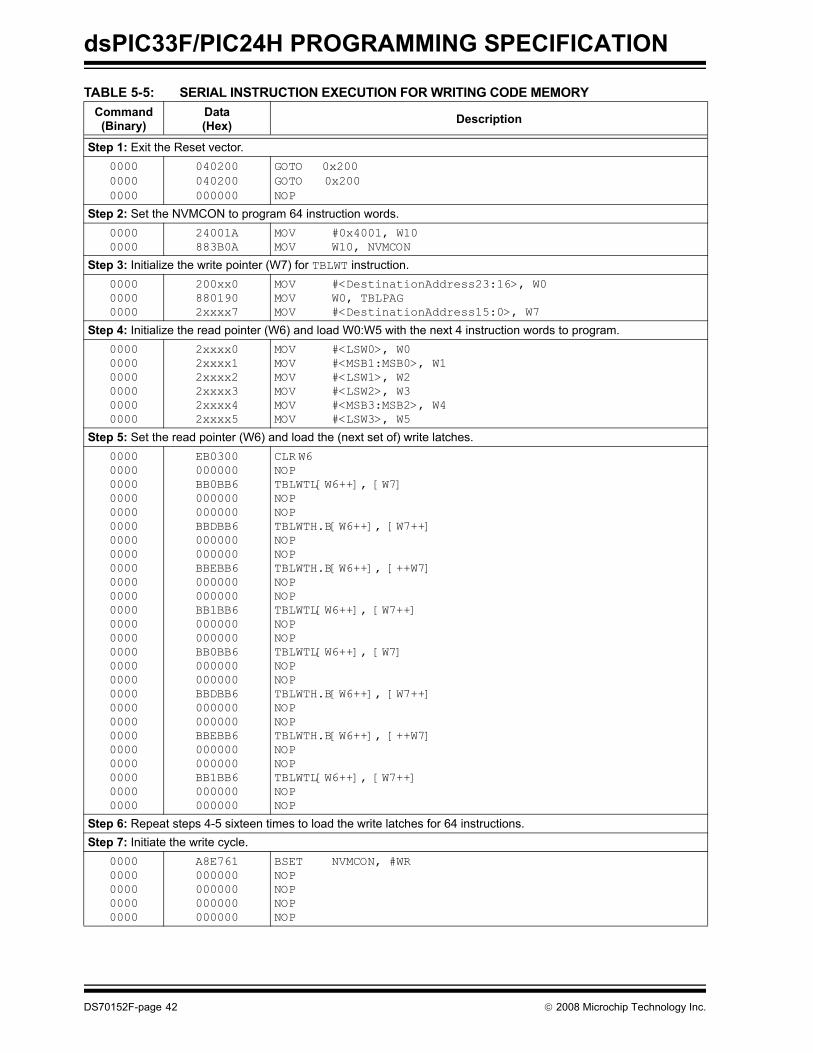
dsPIC33F/PIC24H PROGRAMMING SPECIFICATION
TABLE 5-5: SERIAL INSTRUCTION EXECUTION FOR WRITING CODE MEMORYCommand(Binary)
Data(Hex) Description
Step 1: Exit the Reset vector.000000000000
040200040200000000
GOTO 0x200GOTO 0x200NOP
Step 2: Set the NVMCON to program 64 instruction words.00000000
24001A883B0A
MOV #0x4001, W10MOV W10, NVMCON
Step 3: Initialize the write pointer (W7) for TBLWT instruction.000000000000
200xx08801902xxxx7
MOV #<DestinationAddress23:16>, W0MOV W0, TBLPAGMOV #<DestinationAddress15:0>, W7
Step 4: Initialize the read pointer (W6) and load W0:W5 with the next 4 instruction words to program.000000000000000000000000
2xxxx02xxxx12xxxx22xxxx32xxxx42xxxx5
MOV #<LSW0>, W0MOV #<MSB1:MSB0>, W1MOV #<LSW1>, W2MOV #<LSW2>, W3MOV #<MSB3:MSB2>, W4MOV #<LSW3>, W5
Step 5: Set the read pointer (W6) and load the (next set of) write latches.00000000000000000000000000000000000000000000000000000000000000000000000000000000000000000000000000000000
EB0300000000BB0BB6000000000000BBDBB6000000000000BBEBB6000000000000BB1BB6000000000000BB0BB6000000000000BBDBB6000000000000BBEBB6000000000000BB1BB6000000000000
CLR W6NOPTBLWTL[W6++], [W7] NOPNOPTBLWTH.B[W6++], [W7++] NOPNOPTBLWTH.B[W6++], [++W7] NOPNOPTBLWTL[W6++], [W7++] NOP NOPTBLWTL[W6++], [W7] NOPNOPTBLWTH.B[W6++], [W7++] NOP NOPTBLWTH.B[W6++], [++W7] NOPNOPTBLWTL[W6++], [W7++] NOPNOP
Step 6: Repeat steps 4-5 sixteen times to load the write latches for 64 instructions.Step 7: Initiate the write cycle.
00000000000000000000
A8E761000000000000000000000000
BSET NVMCON, #WR NOPNOPNOPNOP
DS70152F-page 42 © 2008 Microchip Technology Inc.
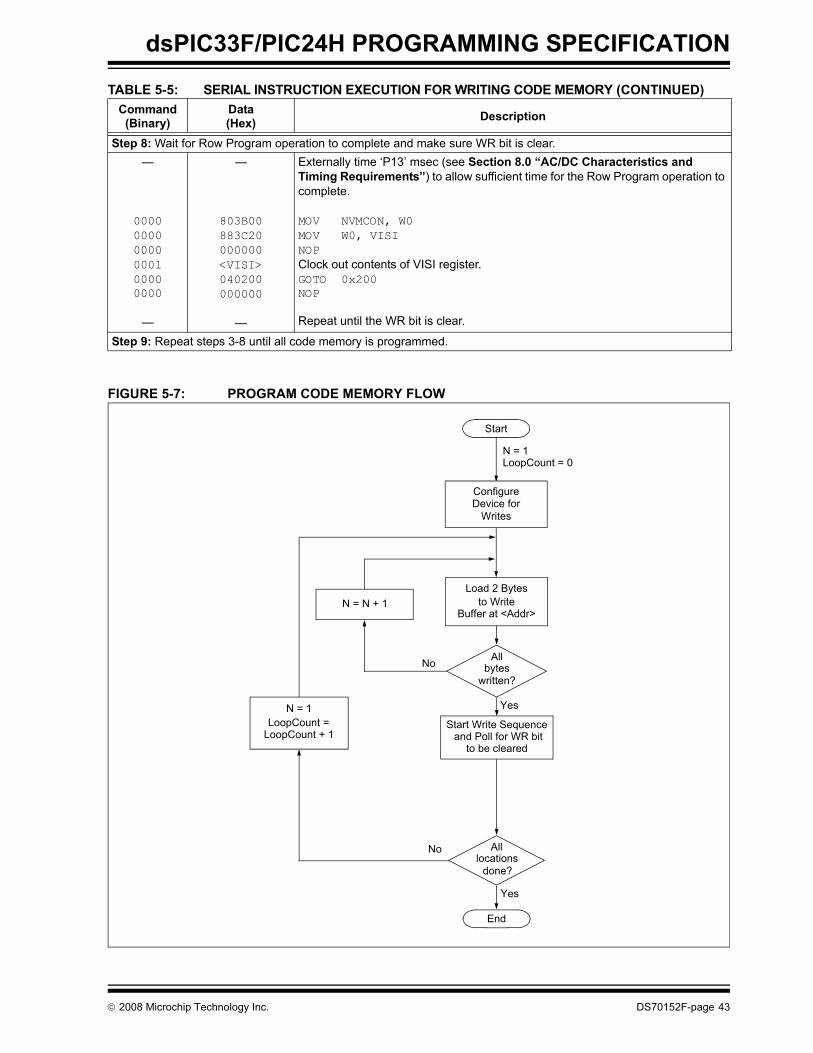
dsPIC33F/PIC24H PROGRAMMING SPECIFICATION
FIGURE 5-7: PROGRAM CODE MEMORY FLOW
Step 8: Wait for Row Program operation to complete and make sure WR bit is clear.—
000000000000000100000000
—
—
803B00883C20000000<VISI>040200000000
—
Externally time ‘P13’ msec (see Section 8.0 “AC/DC Characteristics and Timing Requirements”) to allow sufficient time for the Row Program operation to complete.
MOV NVMCON, W0MOV W0, VISINOPClock out contents of VISI register.GOTO 0x200NOP
Repeat until the WR bit is clear.
Step 9: Repeat steps 3-8 until all code memory is programmed.
TABLE 5-5: SERIAL INSTRUCTION EXECUTION FOR WRITING CODE MEMORY (CONTINUED)Command(Binary)
Data(Hex) Description
Start Write Sequence
Alllocations
done?
No
End
Start
Yes
Load 2 Bytesto Write
Buffer at <Addr>
Allbytes
written?No
Yes
and Poll for WR bitto be cleared
N = 1LoopCount = 0
ConfigureDevice for
Writes
N = 1LoopCount =
LoopCount + 1
N = N + 1
© 2008 Microchip Technology Inc. DS70152F-page 43
dsPIC33F/PIC24H PROGRAMMING SPECIFICATION
5.7 Writing Configuration MemoryThe 8-bit Configuration registers are programmable, oneregister at a time. The default programming valuesrecommended for the Configuration registers are shownin Table 5-7, Table 5-8, and Table 5-9. Therecommended default FOSCSEL value is 0x07, whichselects the FRC clock oscillator setting.
The FBS, FSS and FGS Configuration registers arespecial since they enable code protection for thedevice. For security purposes, once any bit in theseregisters is programmed to ‘0’ (to enable codeprotection), it can only be set back to ‘1’ by performinga Bulk Erase as described in Section 5.5 “ErasingProgram Memory”. Programming any of these bitsfrom a ‘0’ to ‘1’ is not possible, but they may beprogrammed from a ‘1’ to ‘0’ to enable code protection.
TABLE 5-6: DEFAULT CONFIGURATION REGISTER VALUES FOR dsPIC33FJ06GS101/102/202 AND dsPIC33FJ16GS402/404/502/504 DEVICES
TABLE 5-7: DEFAULT CONFIGURATION REGISTER VALUES FOR dsPIC33FJ12GP201/202, dsPIC33FJ12MC201/202, PIC24HJ12GP201/202, dsPIC33FJ32GP202/204, dsPIC33FJ32MC202/204, PIC24HJ32GP202/204, dsPIC33FJ16GP304, dsPIC33FJ16MC304, PIC24HJ16GP304, dsPIC33FJ32GP302/304, dsPIC33FJ32MC302/304 AND PIC24HJ32GP302/304 DEVICES
Table 5-10 shows the ICSP programming details forclearing the Configuration registers. In Step 1, theReset vector is exited. In Step 2, the write pointer (W7)is loaded with 0x0000, which is the original destinationaddress (in TBLPAG, 0xF8 of program memory). InStep 3, the NVMCON is set to program oneConfiguration register. In Step 4, the TBLPAG registeris initialized to 0xF8 for writing to the Configurationregisters. In Step 5, the value to write to eachConfiguration register is loaded to W0. In Step 6, theConfiguration register data is written to the write latchusing the TBLWTL instruction. In Steps 7 and 8, theprogramming cycle is initiated. In Step 9, the internalPC is set to 0x200 as a safety measure to prevent thePC from incrementing into unimplemented memory.Lastly, Steps 4-9 are repeated until all twelveConfiguration registers are written.
Address Name Default Value
0xF80000 FBS 0x0F0xF80004 FGS 0x070xF80006 FOSCSEL 0x870xF80008 FOSC 0xE70xF8000A FWDT 0xDF0xF8000C FPOR 0x0F0xF8000E FICD 0xE30xF80010 FUID0 0xFF0xF80012 FUID1 0xFF0xF80014 FUID2 0xFF0xF80016 FUID3 0xFF
Address Name Default Value
0xF80000 FBS 0x0F0xF80004 FGS 0x070xF80006 FOSCSEL 0x870xF80008 FOSC 0xE7 0xF8000A FWDT 0xDF0xF8000C FPOR 0xF70xF8000E FICD 0xE30xF80010 FUID0 0xFF0xF80012 FUID1 0xFF0xF80014 FUID2 0xFF0xF80016 FUID3 0xFF
DS70152F-page 44 © 2008 Microchip Technology Inc.

dsPIC33F/PIC24H PROGRAMMING SPECIFICATION
TABLE 5-8: DEFAULT CONFIGURATION REGISTER VALUES FOR dsPIC33FJ64GPX02/X04, dsPIC33FJ64MCX02/X04, PIC24HJ128GPX02/X04, dsPIC33FJ128GPX02/X04, dsPIC33FJ128MCX02/X04 AND PIC24HJ128GPX02/X04 DEVICES
TABLE 5-9: DEFAULT CONFIGURATION REGISTER VALUES FOR ALL OTHER DEVICES
Address Name Default Value
0xF80000 FBS 0xCF0xF80002 FSS 0xCF0xF80004 FGS 0x070xF80006 FOSCSEL 0x870xF80008 FOSC 0xE70xF8000A FWDT 0xDF0xF8000C FPOR 0xF70xF8000E FICD 0xE30xF80010 FUID0 0xFF0xF80012 FUID1 0xFF0xF80014 FUID2 0xFF0xF80016 FUID3 0xFF
Address Name Default Value
0xF80000 FBS 0xCF0xF80002 FSS 0xCF0xF80004 FGS 0x070xF80006 FOSCSEL 0xA70xF80008 FOSC 0xC70xF8000A FWDT 0xDF0xF8000C FPOR 0xE70xF8000E FICD 0xE30xF80010 FUID0 0xFF0xF80012 FUID1 0xFF0xF80014 FUID2 0xFF0xF80016 FUID3 0xFF
© 2008 Microchip Technology Inc. DS70152F-page 45

dsPIC33F/PIC24H PROGRAMMING SPECIFICATION
TABLE 5-10: SERIAL INSTRUCTION EXECUTION FOR WRITING CONFIGURATION REGISTERSCommand(Binary)
Data(Hex) Description
Step 1: Exit the Reset vector.000000000000
040200040200000000
GOTO 0x200GOTO 0x200NOP
Step 2: Initialize the write pointer (W7) for the TBLWT instruction.0000 200007 MOV #0x0000, W7
Step 3: Set the NVMCON register to program one Configuration register.00000000
24000A883B0A
MOV #0x4000, W10MOV W10, NVMCON
Step 4: Initialize the TBLPAG register.00000000
200F80880190
MOV #0xF8, W0MOV W0, TBLPAG
Step 5: Load the Configuration register data to W6.0000 2xxxx0 MOV #<CONFIG_VALUE>, W0
Step 6: Write the Configuration register data to the write latch and increment the write pointer.000000000000
BB1B80000000000000
TBLWTL W0, [W7++]NOPNOP
Step 7: Initiate the write cycle.00000000000000000000
A8E761000000000000000000000000
BSET NVMCON, #WRNOPNOPNOPNOP
Step 8: Wait for the Configuration Register Write operation to complete and make sure WR bit is clear.—
0000000000000001
00000000
—
—
803B00883C20000000<VISI>
040200000000
—
Externally time ‘P20’ msec (see Section 8.0 “AC/DC Characteristics and Timing Requirements”) to allow sufficient time for the Configuration Register Write operation to complete.
MOV NVMCON, W0MOV W0, VISINOPClock out contents of VISI register.
GOTO 0x200NOP
Repeat until the WR bit is clear.Step 9: Repeat steps 5-8 until all twelve Configuration registers are written.
DS70152F-page 46 © 2008 Microchip Technology Inc.
dsPIC33F/PIC24H PROGRAMMING SPECIFICATION
5.8 Reading Code MemoryReading from code memory is performed by executinga series of TBLRD instructions and clocking out the datausing the REGOUT command.
Table 5-11 shows the ICSP programming details forreading code memory. In Step 1, the Reset vector isexited. In Step 2, the 24-bit starting source address forreading is loaded into the TBLPAG register and W6register. The upper byte of the starting source addressis stored in TBLPAG and the lower 16 bits of the sourceaddress are stored in W6.
To minimize the reading time, the packed instructionword format that was utilized for writing is also used forreading (see Figure 5-6). In Step 3, the write pointer,W7, is initialized. In Step 4, two instruction words areread from code memory and clocked out of the device,through the VISI register, using the REGOUT command.Step 4 is repeated until the desired amount of codememory is read.
TABLE 5-11: SERIAL INSTRUCTION EXECUTION FOR READING CODE MEMORYCommand(Binary)
Data(Hex) Description
Step 1: Exit the Reset vector.000000000000
040200040200000000
GOTO 0x200GOTO 0x200NOP
Step 2: Initialize TBLPAG and the read pointer (W6) for TBLRD instruction.000000000000
200xx08801902xxxx6
MOV #<SourceAddress23:16>, W0MOV W0, TBLPAGMOV #<SourceAddress15:0>, W6
Step 3: Initialize the write pointer (W7) and store the next four locations of code memory to W0:W5.00000000000000000000000000000000000000000000000000000000000000000000000000000000000000000000000000000000
EB0380000000BA1B96000000000000BADBB6000000000000BADBD6000000000000BA1BB6000000000000BA1B96000000000000BADBB6000000000000BADBD6000000000000BA0BB6000000000000
CLR W7 NOPTBLRDL [W6], [W7++] NOPNOPTBLRDH.B [W6++], [W7++] NOPNOPTBLRDH.B [++W6], [W7++] NOPNOPTBLRDL [W6++], [W7++] NOPNOPTBLRDL [W6], [W7++] NOPNOPTBLRDH.B [W6++], [W7++] NOPNOPTBLRDH.B [++W6], [W7++] NOPNOPTBLRDL [W6++], [W7] NOPNOP
© 2008 Microchip Technology Inc. DS70152F-page 47

dsPIC33F/PIC24H PROGRAMMING SPECIFICATION
Step 4: Output W0:W5 using the VISI register and REGOUT command.000000000001000000000000000100000000000000010000000000000001000000000000000100000000000000010000
883C20000000<VISI>000000883C21000000<VISI>000000883C22000000<VISI>000000883C23000000<VISI>000000883C24000000<VISI>000000883C25000000<VISI>000000
MOV W0, VISI NOPClock out contents of VISI register.NOPMOV W1, VISI NOPClock out contents of VISI register.NOPMOV W2, VISI NOPClock out contents of VISI register.NOPMOV W3, VISI NOPClock out contents of VISI register.NOPMOV W4, VISI NOPClock out contents of VISI register.NOPMOV W5, VISI NOPClock out contents of VISI register.NOP
Step 5: Repeat step 4 until all desired code memory is read.Step 6: Reset device internal PC.
00000000
040200000000
GOTO 0x200 NOP
TABLE 5-11: SERIAL INSTRUCTION EXECUTION FOR READING CODE MEMORY (CONTINUED)Command(Binary)
Data(Hex) Description
DS70152F-page 48 © 2008 Microchip Technology Inc.

dsPIC33F/PIC24H PROGRAMMING SPECIFICATION
5.9 Reading Configuration MemoryThe procedure for reading configuration memory issimilar to the procedure for reading code memory,except that 16-bit data words are read (with the upperbyte read being all ‘0’s) instead of 24-bit words. Sincethere are twelve Configuration registers, they are readone register at a time.
Table 5-12 shows the ICSP programming details forreading all of the configuration memory. Note that theTBLPAG register is hard coded to 0xF8 (the upper byteaddress of configuration memory) and the read pointer,W6, is initialized to 0x0000.
TABLE 5-12: SERIAL INSTRUCTION EXECUTION FOR READING ALL CONFIGURATION MEMORYCommand(Binary)
Data(Hex) Description
Step 1: Exit the Reset vector.000000000000
040200040200000000
GOTO 0x200GOTO 0x200NOP
Step 2: Initialize TBLPAG, the read pointer (W6) and the write pointer (W7) for TBLRD instruction.00000000000000000000
200F80880190EB0300207847000000
MOV #0xF8, W0MOV W0, TBLPAGCLR W6MOV #VISI, W7NOP
Step 3: Read the Configuration register and write it to the VISI register (located at 0x784) and clock out the VISI register using the REGOUT command.
0000000000000001
BA0BB6000000000000<VISI>
TBLRDL [W6++], [W7] NOP NOPClock out contents of VISI register.
Step 4: Repeat step 3 twelve times to read all the Configuration registers.Step 5: Reset device internal PC.
00000000
040200000000
GOTO 0x200 NOP
© 2008 Microchip Technology Inc. DS70152F-page 49
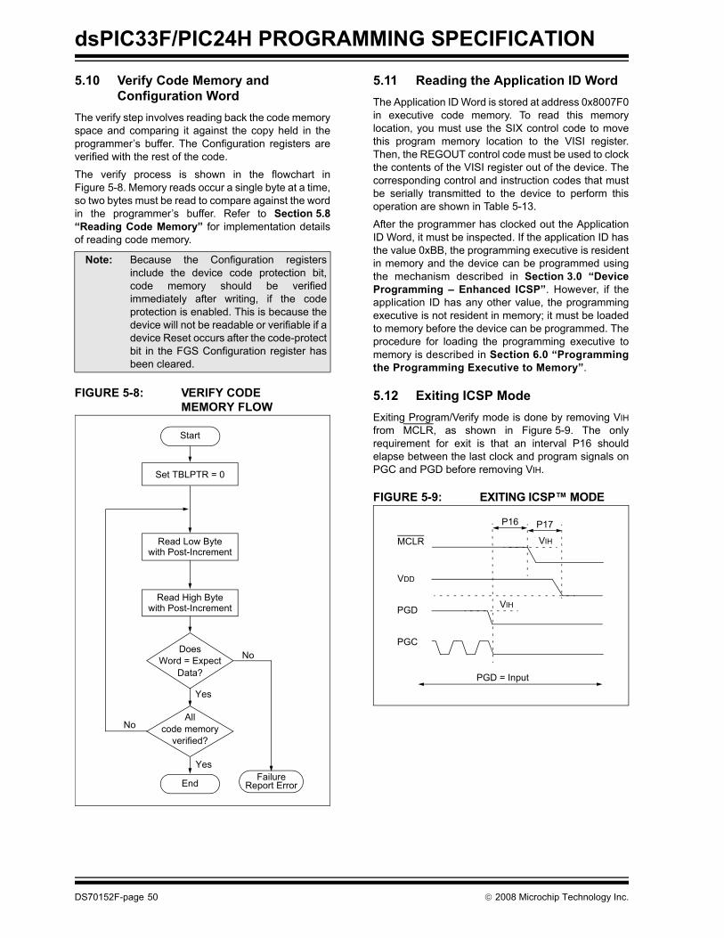
dsPIC33F/PIC24H PROGRAMMING SPECIFICATION
5.10 Verify Code Memory and Configuration Word
The verify step involves reading back the code memoryspace and comparing it against the copy held in theprogrammer’s buffer. The Configuration registers areverified with the rest of the code.
The verify process is shown in the flowchart inFigure 5-8. Memory reads occur a single byte at a time,so two bytes must be read to compare against the wordin the programmer’s buffer. Refer to Section 5.8“Reading Code Memory” for implementation detailsof reading code memory.
FIGURE 5-8: VERIFY CODE MEMORY FLOW
5.11 Reading the Application ID WordThe Application ID Word is stored at address 0x8007F0in executive code memory. To read this memorylocation, you must use the SIX control code to movethis program memory location to the VISI register.Then, the REGOUT control code must be used to clockthe contents of the VISI register out of the device. Thecorresponding control and instruction codes that mustbe serially transmitted to the device to perform thisoperation are shown in Table 5-13.
After the programmer has clocked out the ApplicationID Word, it must be inspected. If the application ID hasthe value 0xBB, the programming executive is residentin memory and the device can be programmed usingthe mechanism described in Section 3.0 “DeviceProgramming – Enhanced ICSP”. However, if theapplication ID has any other value, the programmingexecutive is not resident in memory; it must be loadedto memory before the device can be programmed. Theprocedure for loading the programming executive tomemory is described in Section 6.0 “Programmingthe Programming Executive to Memory”.
5.12 Exiting ICSP ModeExiting Program/Verify mode is done by removing VIHfrom MCLR, as shown in Figure 5-9. The onlyrequirement for exit is that an interval P16 shouldelapse between the last clock and program signals onPGC and PGD before removing VIH.
FIGURE 5-9: EXITING ICSP™ MODE
Note: Because the Configuration registersinclude the device code protection bit,code memory should be verifiedimmediately after writing, if the codeprotection is enabled. This is because thedevice will not be readable or verifiable if adevice Reset occurs after the code-protectbit in the FGS Configuration register hasbeen cleared.
Read Low Byte
Read High Byte
DoesWord = Expect
Data?
Allcode memory
verified?
No
Yes
No
Set TBLPTR = 0
Start
Yes
End
with Post-Increment
with Post-Increment
FailureReport Error
MCLR
P16
PGD
PGD = Input
PGC
VDD
VIH
VIH
P17
DS70152F-page 50 © 2008 Microchip Technology Inc.
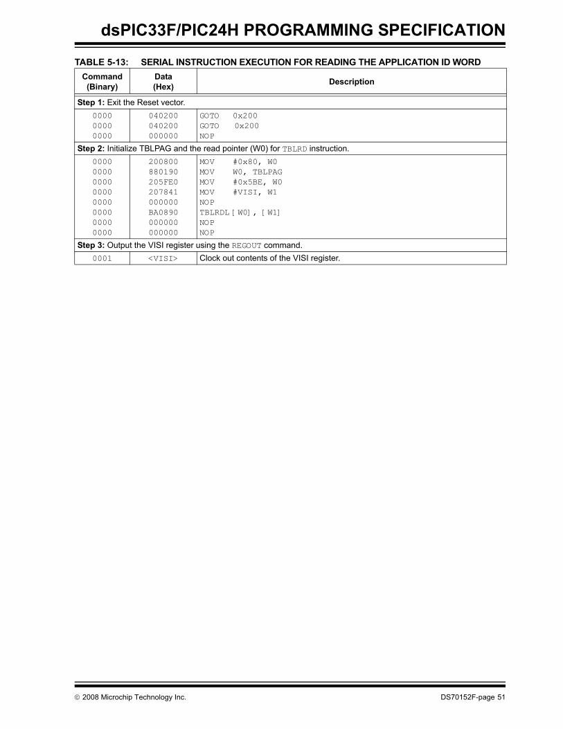
dsPIC33F/PIC24H PROGRAMMING SPECIFICATION
TABLE 5-13: SERIAL INSTRUCTION EXECUTION FOR READING THE APPLICATION ID WORDCommand(Binary)
Data(Hex) Description
Step 1: Exit the Reset vector.000000000000
040200040200000000
GOTO 0x200GOTO 0x200NOP
Step 2: Initialize TBLPAG and the read pointer (W0) for TBLRD instruction.00000000000000000000000000000000
200800880190205FE0207841000000BA0890000000000000
MOV #0x80, W0 MOV W0, TBLPAGMOV #0x5BE, W0 MOV #VISI, W1 NOP TBLRDL [W0], [W1] NOPNOP
Step 3: Output the VISI register using the REGOUT command.0001 <VISI> Clock out contents of the VISI register.
© 2008 Microchip Technology Inc. DS70152F-page 51

dsPIC33F/PIC24H PROGRAMMING SPECIFICATION
6.0 PROGRAMMING THE PROGRAMMING EXECUTIVE TO MEMORY
6.1 OverviewIf it is determined that the programming executive is notpresent in executive memory (as described inSection 3.2 “Confirming the Presence of theProgramming Executive”), it must be programmedinto executive memory using ICSP, as described inSection 5.0 “Device Programming – ICSP”.
Storing the programming executive to executivememory is similar to normal programming of codememory. Namely, the executive memory must first beerased, and then the programming executive must beprogrammed 64 words at a time. This control flow issummarized in Table 6-1.
TABLE 6-1: PROGRAMMING THE PROGRAMMING EXECUTIVECommand(Binary)
Data(Hex) Description
Step 1: Exit the Reset vector and erase executive memory.000000000000
040200040200000000
GOTO 0x200GOTO 0x200NOP
Step 2: Initialize the NVMCON to erase a page of executive memory.00000000
24072A883B0A
MOV #0x4042, W10 MOV W10, NVMCON
Step 3: Initiate the erase cycle, wait for erase to complete and make sure WR bit is clear.00000000000000000000
—
0000000000000001
A8E761000000000000000000000000
—
803B00883C20000000<VISI>
BSET NVMCON, #15 NOPNOPNOPNOP
Externally time ‘P12’ msec (see Section 8.0 “AC/DC Characteristics and Timing Requirements”) to allow sufficient time for the Page Erase operation to complete.
MOV NVMCON, W0MOV W0, VISINOPClock out contents of VISI register. Repeat until the WR bit is clear.
Step 4: Repeat Step 3 four times to erase all four pages of executive memory. Step 5: Initialize the NVMCON to program 64 instruction words.
00000000
24001A883B0A
MOV #0x4001, W10 MOV W10, NVMCON
Step 6: Initialize TBLPAG and the write pointer (W7).0000000000000000
200800880190EB0380000000
MOV #0x80, W0 MOV W0, TBLPAG CLR W7 NOP
DS70152F-page 52 © 2008 Microchip Technology Inc.

dsPIC33F/PIC24H PROGRAMMING SPECIFICATION
Step 7: Load W0:W5 with the next 4 words of packed programming executive code and initialize W6 for programming. Programming starts from the base of executive memory (0x800000) using W6 as a read pointer and W7 as a write pointer.
000000000000000000000000
2<LSW0>02<MSB1:MSB0>12<LSW1>22<LSW2>32<MSB3:MSB2>42<LSW3>5
MOV #<LSW0>, W0 MOV #<MSB1:MSB0>, W1 MOV #<LSW1>, W2 MOV #<LSW2>, W3 MOV #<MSB3:MSB2>, W4 MOV #<LSW3>, W5
Step 8: Set the read pointer (W6) and load the (next four write) latches.00000000000000000000000000000000000000000000000000000000000000000000000000000000000000000000000000000000
EB0300000000BB0BB6000000000000BBDBB6000000000000BBEBB6000000000000BB1BB6000000000000BB0BB6000000000000BBDBB6000000000000BBEBB6000000000000BB1BB6000000000000
CLR W6NOPTBLWTL [W6++], [W7] NOPNOPTBLWTH.B[W6++], [W7++] NOPNOPTBLWTH.B[W6++], [++W7] NOPNOPTBLWTL [W6++], [W7++] NOPNOPTBLWTL [W6++], [W7] NOPNOPTBLWTH.B[W6++], [W7++] NOPNOPTBLWTH.B[W6++], [++W7] NOPNOPTBLWTL [W6++], [W7++] NOPNOP
Step 9: Repeat Steps 7-8 sixteen times to load the write latches for the 64 instructions.Step 10: Initiate the programming cycle.
00000000000000000000
A8E761000000000000000000000000
BSET NVMCON, #15 NOPNOPNOPNOP
Step 11: Wait for the Row Program operation to complete.
TABLE 6-1: PROGRAMMING THE PROGRAMMING EXECUTIVE (CONTINUED)Command(Binary)
Data(Hex) Description
© 2008 Microchip Technology Inc. DS70152F-page 53
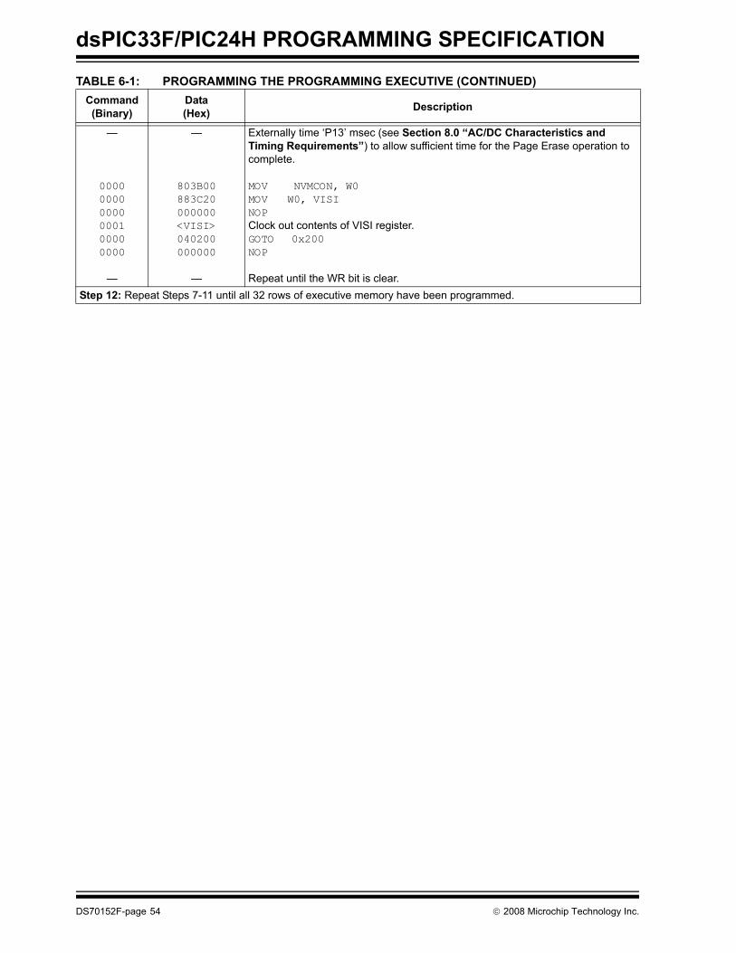
dsPIC33F/PIC24H PROGRAMMING SPECIFICATION
—
000000000000000100000000
—
—
803B00883C20000000<VISI>040200000000
—
Externally time ‘P13’ msec (see Section 8.0 “AC/DC Characteristics and Timing Requirements”) to allow sufficient time for the Page Erase operation to complete.
MOV NVMCON, W0MOV W0, VISINOPClock out contents of VISI register.GOTO 0x200 NOP
Repeat until the WR bit is clear.Step 12: Repeat Steps 7-11 until all 32 rows of executive memory have been programmed.
TABLE 6-1: PROGRAMMING THE PROGRAMMING EXECUTIVE (CONTINUED)Command(Binary)
Data(Hex) Description
DS70152F-page 54 © 2008 Microchip Technology Inc.

dsPIC33F/PIC24H PROGRAMMING SPECIFICATION
6.2 Programming Verification After the programming executive has beenprogrammed to executive memory using ICSP, it mustbe verified. Verification is performed by reading out thecontents of executive memory and comparing it withthe image of the programming executive stored in theprogrammer.
Reading the contents of executive memory can beperformed using the same technique described inSection 5.8 “Reading Code Memory”. A procedurefor reading executive memory is shown in Table 6-2.Note that in Step 2, the TBLPAG register is set to 0x80,such that executive memory may be read.
TABLE 6-2: READING EXECUTIVE MEMORYCommand(Binary)
Data(Hex) Description
Step 1: Exit the Reset vector.000000000000
040200040200000000
GOTO 0x200GOTO 0x200NOP
Step 2: Initialize TBLPAG and the read pointer (W6) for TBLRD instruction.000000000000
200800880190EB0300
MOV #0x80, W0 MOV W0, TBLPAGCLR W6
Step 3: Initialize the write pointer (W7) and store the next four locations of code memory to W0:W5.00000000000000000000000000000000000000000000000000000000000000000000000000000000000000000000000000000000
EB0380000000BA1B96000000000000BADBB6000000000000BADBD6000000000000BA1BB6000000000000BA1B96000000000000BADBB6000000000000BADBD6000000000000BA0BB6000000000000
CLR W7 NOPTBLRDL [W6], [W7++] NOPNOPTBLRDH.B [W6++], [W7++] NOPNOPTBLRDH.B [++W6], [W7++] NOPNOPTBLRDL [W6++], [W7++] NOPNOPTBLRDL [W6], [W7++] NOPNOPTBLRDH.B [W6++], [W7++] NOPNOPTBLRDH.B [++W6], [W7++] NOPNOPTBLRDL [W6++], [W7] NOPNOP
© 2008 Microchip Technology Inc. DS70152F-page 55
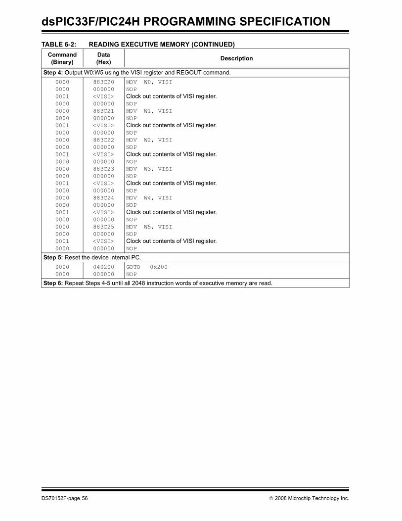
dsPIC33F/PIC24H PROGRAMMING SPECIFICATION
Step 4: Output W0:W5 using the VISI register and REGOUT command.000000000001000000000000000100000000000000010000000000000001000000000000000100000000000000010000
883C20000000<VISI>000000883C21000000<VISI>000000883C22000000<VISI>000000883C23000000<VISI>000000883C24000000<VISI>000000883C25000000<VISI>000000
MOV W0, VISI NOPClock out contents of VISI register.NOPMOV W1, VISI NOPClock out contents of VISI register.NOPMOV W2, VISI NOPClock out contents of VISI register.NOPMOV W3, VISI NOPClock out contents of VISI register.NOPMOV W4, VISI NOPClock out contents of VISI register.NOPMOV W5, VISI NOPClock out contents of VISI register.NOP
Step 5: Reset the device internal PC.00000000
040200000000
GOTO 0x200 NOP
Step 6: Repeat Steps 4-5 until all 2048 instruction words of executive memory are read.
TABLE 6-2: READING EXECUTIVE MEMORY (CONTINUED)Command(Binary)
Data(Hex) Description
DS70152F-page 56 © 2008 Microchip Technology Inc.

dsPIC33F/PIC24H PROGRAMMING SPECIFICATION
7.0 DEVICE IDThe device ID region of memory can be used todetermine mask, variant and manufacturinginformation about the chip. The device ID region is2 x 16 bits and it can be read using the READCcommand. This region of memory is read-only and canalso be read when code protection is enabled.
Table 7-1 shows the device ID for each device andTable 7-2 shows the Device ID registers.
TABLE 7-1: DEVICE IDs AND REVISION
Device DEVID Register Value DEVREV Register Value and Silicon Revision
dsPIC33FJ06GS101 0x0C00 0x3000 - A1 RevisiondsPIC33FJ06GS102 0x0C01dsPIC33FJ06GS202 0x0C02dsPIC33FJ16GS402 0x0C04dsPIC33FJ16GS404 0x0C06dsPIC33FJ16GS502 0x0C03dsPIC33FJ01GS504 0x0C05dsPIC33FJ12GP201 0x0802 0x3001 - A2 RevisiondsPIC33FJ12GP202 0x0803 0x3002 - A3 RevisiondsPIC33FJ12MC201 0x0800dsPIC33FJ12MC202 0x0801PIC24HJ12GP201 0x080APIC24HJ12GP202 0x080B
dsPIC33FJ16GP304 0x0F07dsPIC33FJ16MC304 0x0F03PIC24HJ16GP304 0x0F17
dsPIC33FJ32GP202 0x0F0DdsPIC33FJ32GP204 0x0F0FdsPIC33FJ32MC202 0x0F09dsPIC33FJ32MC204 0x0F0BPIC24HJ32GP202 0x0F1DPIC24HJ32GP204 0x0F1F
dsPIC33FJ64GP206 0x00C1 0x3002 - A2 RevisiondsPIC33FJ64GP306 0x00CD 0x3003 - B0 RevisiondsPIC33FJ64GP310 0x00CF 0x3004 - A3 RevisiondsPIC33FJ64GP706 0x00D5 0x3006 - B1 RevisiondsPIC33FJ64GP708 0x00D6 0x3007 - B2 RevisiondsPIC33FJ64GP710 0x00D7dsPIC33FJ64MC506 0x0089dsPIC33FJ64MC508 0x008AdsPIC33FJ64MC510 0x008BdsPIC33FJ64MC706 0x0091dsPIC33FJ64MC710 0x0097PIC24HJ64GP206 0x0041PIC24HJ64GP210 0x0047PIC24HJ64GP506 0x0049PIC24HJ64GP510 0x004B
© 2008 Microchip Technology Inc. DS70152F-page 57
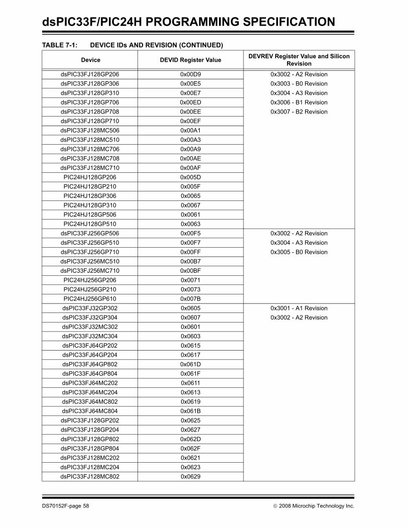
dsPIC33F/PIC24H PROGRAMMING SPECIFICATION
dsPIC33FJ128GP206 0x00D9 0x3002 - A2 RevisiondsPIC33FJ128GP306 0x00E5 0x3003 - B0 RevisiondsPIC33FJ128GP310 0x00E7 0x3004 - A3 RevisiondsPIC33FJ128GP706 0x00ED 0x3006 - B1 RevisiondsPIC33FJ128GP708 0x00EE 0x3007 - B2 RevisiondsPIC33FJ128GP710 0x00EFdsPIC33FJ128MC506 0x00A1dsPIC33FJ128MC510 0x00A3dsPIC33FJ128MC706 0x00A9dsPIC33FJ128MC708 0x00AEdsPIC33FJ128MC710 0x00AFPIC24HJ128GP206 0x005DPIC24HJ128GP210 0x005FPIC24HJ128GP306 0x0065PIC24HJ128GP310 0x0067PIC24HJ128GP506 0x0061PIC24HJ128GP510 0x0063
dsPIC33FJ256GP506 0x00F5 0x3002 - A2 RevisiondsPIC33FJ256GP510 0x00F7 0x3004 - A3 RevisiondsPIC33FJ256GP710 0x00FF 0x3005 - B0 RevisiondsPIC33FJ256MC510 0x00B7dsPIC33FJ256MC710 0x00BFPIC24HJ256GP206 0x0071PIC24HJ256GP210 0x0073PIC24HJ256GP610 0x007BdsPIC33FJ32GP302 0x0605 0x3001 - A1 RevisiondsPIC33FJ32GP304 0x0607 0x3002 - A2 RevisiondsPIC33FJ32MC302 0x0601dsPIC33FJ32MC304 0x0603dsPIC33FJ64GP202 0x0615dsPIC33FJ64GP204 0x0617dsPIC33FJ64GP802 0x061DdsPIC33FJ64GP804 0x061FdsPIC33FJ64MC202 0x0611dsPIC33FJ64MC204 0x0613dsPIC33FJ64MC802 0x0619dsPIC33FJ64MC804 0x061BdsPIC33FJ128GP202 0x0625dsPIC33FJ128GP204 0x0627dsPIC33FJ128GP802 0x062DdsPIC33FJ128GP804 0x062FdsPIC33FJ128MC202 0x0621dsPIC33FJ128MC204 0x0623dsPIC33FJ128MC802 0x0629
TABLE 7-1: DEVICE IDs AND REVISION (CONTINUED)
Device DEVID Register Value DEVREV Register Value and Silicon Revision
DS70152F-page 58 © 2008 Microchip Technology Inc.
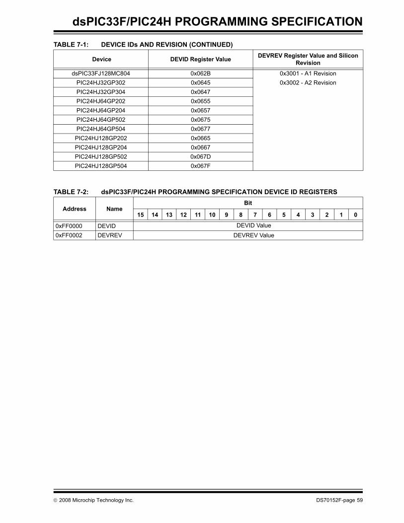
dsPIC33F/PIC24H PROGRAMMING SPECIFICATION
TABLE 7-2: dsPIC33F/PIC24H PROGRAMMING SPECIFICATION DEVICE ID REGISTERS
dsPIC33FJ128MC804 0x062B 0x3001 - A1 RevisionPIC24HJ32GP302 0x0645 0x3002 - A2 RevisionPIC24HJ32GP304 0x0647PIC24HJ64GP202 0x0655PIC24HJ64GP204 0x0657PIC24HJ64GP502 0x0675PIC24HJ64GP504 0x0677PIC24HJ128GP202 0x0665PIC24HJ128GP204 0x0667PIC24HJ128GP502 0x067DPIC24HJ128GP504 0x067F
TABLE 7-1: DEVICE IDs AND REVISION (CONTINUED)
Device DEVID Register Value DEVREV Register Value and Silicon Revision
Address NameBit
15 14 13 12 11 10 9 8 7 6 5 4 3 2 1 0
0xFF0000 DEVID DEVID Value
0xFF0002 DEVREV DEVREV Value
© 2008 Microchip Technology Inc. DS70152F-page 59
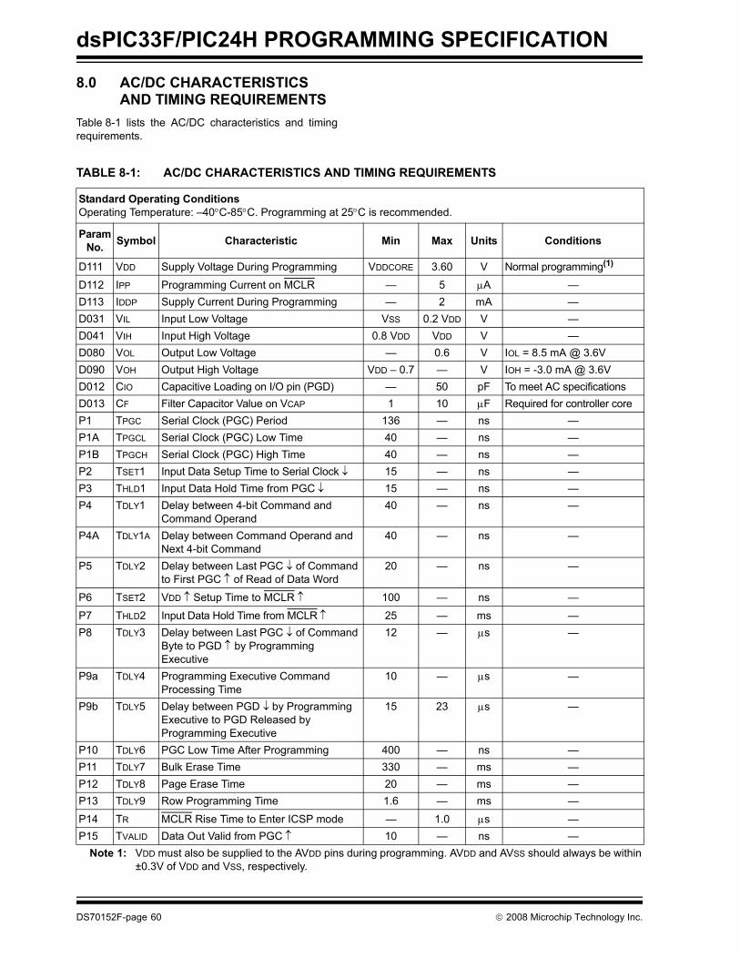
dsPIC33F/PIC24H PROGRAMMING SPECIFICATION
8.0 AC/DC CHARACTERISTICS AND TIMING REQUIREMENTS
Table 8-1 lists the AC/DC characteristics and timingrequirements.
TABLE 8-1: AC/DC CHARACTERISTICS AND TIMING REQUIREMENTS
Standard Operating ConditionsOperating Temperature: –40°C-85°C. Programming at 25°C is recommended.
Param No. Symbol Characteristic Min Max Units Conditions
D111 VDD Supply Voltage During Programming VDDCORE 3.60 V Normal programming(1)
D112 IPP Programming Current on MCLR — 5 μA —D113 IDDP Supply Current During Programming — 2 mA —D031 VIL Input Low Voltage VSS 0.2 VDD V —D041 VIH Input High Voltage 0.8 VDD VDD V —D080 VOL Output Low Voltage — 0.6 V IOL = 8.5 mA @ 3.6VD090 VOH Output High Voltage VDD – 0.7 — V IOH = -3.0 mA @ 3.6VD012 CIO Capacitive Loading on I/O pin (PGD) — 50 pF To meet AC specificationsD013 CF Filter Capacitor Value on VCAP 1 10 μF Required for controller coreP1 TPGC Serial Clock (PGC) Period 136 — ns —P1A TPGCL Serial Clock (PGC) Low Time 40 — ns —P1B TPGCH Serial Clock (PGC) High Time 40 — ns —P2 TSET1 Input Data Setup Time to Serial Clock ↓ 15 — ns —P3 THLD1 Input Data Hold Time from PGC ↓ 15 — ns —P4 TDLY1 Delay between 4-bit Command and
Command Operand40 — ns —
P4A TDLY1A Delay between Command Operand and Next 4-bit Command
40 — ns —
P5 TDLY2 Delay between Last PGC ↓ of Command to First PGC ↑ of Read of Data Word
20 — ns —
P6 TSET2 VDD ↑ Setup Time to MCLR ↑ 100 — ns —
P7 THLD2 Input Data Hold Time from MCLR ↑ 25 — ms —P8 TDLY3 Delay between Last PGC ↓ of Command
Byte to PGD ↑ by Programming Executive
12 — μs —
P9a TDLY4 Programming Executive Command Processing Time
10 — μs —
P9b TDLY5 Delay between PGD ↓ by Programming Executive to PGD Released by Programming Executive
15 23 μs —
P10 TDLY6 PGC Low Time After Programming 400 — ns —P11 TDLY7 Bulk Erase Time 330 — ms —P12 TDLY8 Page Erase Time 20 — ms —P13 TDLY9 Row Programming Time 1.6 — ms —
P14 TR MCLR Rise Time to Enter ICSP mode — 1.0 μs —P15 TVALID Data Out Valid from PGC ↑ 10 — ns —
Note 1: VDD must also be supplied to the AVDD pins during programming. AVDD and AVSS should always be within±0.3V of VDD and VSS, respectively.
DS70152F-page 60 © 2008 Microchip Technology Inc.

dsPIC33F/PIC24H PROGRAMMING SPECIFICATION
P16 TDLY10 Delay between Last PGC ↓ and 0 — s —
P17 THLD3 MCLR ↓ to VDD ↓ — 100 ns —
P18 TKEY1 Delay from First MCLR ↓ to First PGC ↑ for Key Sequence on PGD
40 — ns —
P19 TKEY2 Delay from Last PGC ↓ for Key Sequence on PGD to Second MCLR ↑
25 — ns —
P20 TDLY11 Maximum Wait Time for Configuration Register Programming
— 25 ms —
TABLE 8-1: AC/DC CHARACTERISTICS AND TIMING REQUIREMENTS (CONTINUED)
Standard Operating ConditionsOperating Temperature: –40°C-85°C. Programming at 25°C is recommended.
Param No. Symbol Characteristic Min Max Units Conditions
Note 1: VDD must also be supplied to the AVDD pins during programming. AVDD and AVSS should always be within±0.3V of VDD and VSS, respectively.
© 2008 Microchip Technology Inc. DS70152F-page 61

dsPIC33F/PIC24H PROGRAMMING SPECIFICATION
NOTES:
DS70152F-page 62 © 2008 Microchip Technology Inc.

dsPIC33F/PIC24H PROGRAMMING SPECIFICATION
APPENDIX A: HEX FILE FORMATFlash programmers process the standard HEX formatused by the Microchip development tools. The formatsupported is the Intel® HEX32 Format (INHX32).Please refer to Appendix A in the MPASM Users Guide(DS33014) for more information about hex file formats.
The basic format of the hex file is::BBAAAATTHHHH...HHHHCC
Each data record begins with a 9-character prefix andalways ends with a 2-character checksum. All recordsbegin with ':' regardless of the format. The individualelements are described below.
• BB - is a two-digit hexadecimal byte count representing the number of data bytes that appear on the line. Divide this number by two to get the number of words per line.
• AAAA - is a four-digit hexadecimal address representing the starting address of the data record. Format is high byte first followed by low byte. The address is doubled because this format only supports 8 bits. Divide the value by two to find the real device address.
• TT - is a two-digit record type that will be ‘00’ for data records, ‘01’ for end-of-file records and ‘04’ for extended-address record.
• HHHH - is a four-digit hexadecimal data word. Format is low byte followed by high byte. There will be BB/2 data words following TT.
• CC - is a two-digit hexadecimal checksum that is the two's complement of the sum of all the preceding bytes in the line record.
Because the Intel hex file format is byte-oriented, andthe 16-bit program counter is not, program memorysections require special treatment. Each 24-bitprogram word is extended to 32 bits by inserting aso-called “phantom byte”. Each program memoryaddress is multiplied by 2 to yield a byte address.
As an example, a section that is located at 0x100 inprogram memory will be represented in the hex file as0x200.
The hex file will be produced with the followingcontents:
:020000040000fa
:040200003322110096
:00000001FF
Notice that the data record (line 2) has a load addressof 0200, while the source code specified address0x100. Note also that the data is represented in“little-endian” format, meaning the Least SignificantByte (LSB) appears first. The phantom byte appearslast, just before the checksum.
© 2008 Microchip Technology Inc. DS70152F-page 63
dsPIC33F/PIC24H PROGRAMMING SPECIFICATION
APPENDIX B: REVISION HISTORY
Revision C (June 2006)• Added code protection Configuration register
descriptions• Added information about Unit ID• Added ERASES, ERASEG and ERASEC
programming executive commands• Added checksum computation equation
Revision D (March 2007)• Added information specific to the
dsPIC33FJ12GP201/202, dsPIC33FJ12MC201/202 and PIC24HJ12GP201/202 devices in several sections, including pinout diagrams, program memory sizes and Device ID values
• Added specific checksum computations for all dsPIC33F and PIC24H devices
• Updated ICSP bulk/page erase and row/byte program code examples to show externally timed operation (waiting for specific delay periods)
• Added the P20 timing characteristic• Updated timing characteristics and references to
the timing characteristics• Updated the ICSP code examples
Revision E (June 2007)• Removed list of devices from first page. This
document covers all released dsPIC33F/PIC24H devices, therefore, references to specific devices are included when applicable
• Added information specific to the following new devices in several sections, including program memory sizes, Configuration bit descriptions, checksum computations, Configuration registers, and Device ID values:- dsPIC33FJ32GP202- dsPIC33FJ32GP204- dsPIC33FJ16GP304- dsPIC33FJ32MC202- dsPIC33FJ32MC204- dsPIC33FJ16MC304- PIC24HJ32GP202- PIC24HJ32GP204- PIC24HJ16GP304
• Updated paragraph in Section 2.3 “Pins Used During Programming” to include reference to location of complete pin diagrams
• Renamed Table 2-1 to “Pins Used During Programming”
• Reordered list of devices in Table 2-2, Table 3-2, and Table 7-1 by device family and memory size
• Removed all pin diagrams• Updated checksum information in Table 3-2 for
the following devices:- dsPIC33FJ12GP201- dsPIC33FJ12GP202- dsPIC33FJ12MC201- dsPIC33FJ12MC201- PIC24HJ12GP201- PIC24HJ12GP202
• Added a note to Section 3.6.1 “Overview”• Changed bit 5 of the FOSCSEL register to
unimplemented ( — ) in Table 3-4• Modified the first paragraph of Section 3.6.2
“Programming Methodology”• Added Appendix A: “Hex File Format”
DS70152F-page 64 © 2008 Microchip Technology Inc.

dsPIC33F/PIC24H PROGRAMMING SPECIFICATION
Revision F (March 2008)• Removed Preliminary status from document
footer• Added information specific to the following new
devices in several sections, including program memory sizes, Configuration bit descriptions, checksum computations, Configuration registers and Device ID values:- dsPIC33FJ06GS101- dsPIC33FJ06GS102- dsPIC33FJ06GS202- dsPIC33FJ16GS402- dsPIC33FJ16GS404- dsPIC33FJ16GS502- dsPIC33FJ16GS504- dsPIC33FJ32GP302- dsPIC33FJ32GP304- dsPIC33FJ32MC302- dsPIC33FJ32MC304- dsPIC33FJ64GP202- dsPIC33FJ64GP204- dsPIC33FJ64GP802- dsPIC33FJ64GP804- dsPIC33FJ64MC202- dsPIC33FJ64MC204- dsPIC33FJ64MC802- dsPIC33FJ64MC804- dsPIC33FJ128GP202- dsPIC33FJ128GP204- dsPIC33FJ128GP802- dsPIC33FJ128GP804- dsPIC33FJ128MC202- dsPIC33FJ128MC204- dsPIC33FJ128MC802- dsPIC33FJ128MC804- PIC24HJ32GP302- PIC24HJ32GP304- PIC24HJ64GP202- PIC24HJ64GP204- PIC24HJ64GP502- PIC24HJ64GP504- PIC24HJ128GP202- PIC24HJ128GP204- PIC24HJ128GP502- PIC24HJ128GP504
• Added note to Section 2.2 “Program Memory Write/Erase Requirements” (preserving last eight instruction words of test memory for dsPIC33FJX6GSXXX devices)
• Added BOREN (FPOR<3>) bit to Configuration Register Map and added Note 5 (see Table 3-4)
• Updated Note 1 in Section 5.3.1 “SIX Serial Instruction Execution”
• Updated Note in Section 5.3.2 “REGOUT Serial Instruction execution”
• Updated Figure 5-2• Added Register 5-1• Updated Table 5-7 and Table 5-8• Added Appendix C: “Device ID Register Silicon
Errata Addendum”
© 2008 Microchip Technology Inc. DS70152F-page 65

dsPIC33F/PIC24H PROGRAMMING SPECIFICATION
APPENDIX C: DEVICE ID REGISTER SILICON ERRATA ADDENDUM
This silicon errata issue was previously published in thefollowing documents, which are available from theMicrochip website:
• dsPIC33FJXXXGPX06/X08/X10 Rev. A2 Silicon Errata (DS80306)
• dsPIC33FJXXXMCX06/X08/X10 Rev. A2 Silicon Errata (DS80307)
• PIC24HJXXXGPX06/X08/X10 Rev. A2 Silicon Errata (DS80280)
This issue is being included in this document to furtherassist customers.
1. Module: Device ID Register
On a few devices, the content of the Device IDregister can change from the factory programmeddefault value immediately after RTSP or ICSP™Flash programming.
As a result, development tools will not recognizethese devices and will generate an error messageindicating that the device ID and the device partnumber do not match. Additionally, someperipherals will be reconfigured and will notfunction as described in the device data sheet.
Refer to Section 5. “Flash Programming”(DS70191), of the “dsPIC33F Family ReferenceManual” for an explanation of RTSP and ICSPFlash programming.
Work aroundAll RTSP and ICSP Flash programming routinesmust be modified as follows:
1. No word programming is allowed. Any wordprogramming must be replaced with rowprogramming.
2. During row programming, load write latches asdescribed in 5.4.2.3 “Loading Write Latches”of Section 5. “Flash Programming”(DS70191).
3. After latches are loaded, reload any latchlocation (in a given row) that has 5 LSB set to0x18, with the original data. For example,reload one of the following latch locations withthe desired data:0xXXXX18, 0xXXXX38, 0xXXXX58, 0xXXXX78, 0xXXXX98, 0xXXXXB8, 0xXXXXD8, 0xXXXXF8
4. Start row programming by settingNVMOP<3:0> = ‘0001’ (Memory row programoperation) in the NVMCON register.
5. After row programming is complete, verify thecontents of Flash memory.
6. If Flash verification errors are found, repeatsteps 2 through 5. If Flash verification errorsare found after a second iteration, report thisproblem to Microchip.
Steps 1 through 5 in the work around areimplemented in MPLAB® IDE version 7.61 for theMPLAB ICD 2, MPLAB REAL ICE™ in-circuitemulator and PM3 tools.
DS70152F-page 66 © 2008 Microchip Technology Inc.
Note the following details of the code protection feature on Microchip devices:• Microchip products meet the specification contained in their particular Microchip Data Sheet.
• Microchip believes that its family of products is one of the most secure families of its kind on the market today, when used in the intended manner and under normal conditions.
• There are dishonest and possibly illegal methods used to breach the code protection feature. All of these methods, to our knowledge, require using the Microchip products in a manner outside the operating specifications contained in Microchip’s Data Sheets. Most likely, the person doing so is engaged in theft of intellectual property.
• Microchip is willing to work with the customer who is concerned about the integrity of their code.
• Neither Microchip nor any other semiconductor manufacturer can guarantee the security of their code. Code protection does not mean that we are guaranteeing the product as “unbreakable.”
Code protection is constantly evolving. We at Microchip are committed to continuously improving the code protection features of ourproducts. Attempts to break Microchip’s code protection feature may be a violation of the Digital Millennium Copyright Act. If such actsallow unauthorized access to your software or other copyrighted work, you may have a right to sue for relief under that Act.
Information contained in this publication regarding deviceapplications and the like is provided only for your convenienceand may be superseded by updates. It is your responsibility toensure that your application meets with your specifications.MICROCHIP MAKES NO REPRESENTATIONS ORWARRANTIES OF ANY KIND WHETHER EXPRESS ORIMPLIED, WRITTEN OR ORAL, STATUTORY OROTHERWISE, RELATED TO THE INFORMATION,INCLUDING BUT NOT LIMITED TO ITS CONDITION,QUALITY, PERFORMANCE, MERCHANTABILITY ORFITNESS FOR PURPOSE. Microchip disclaims all liabilityarising from this information and its use. Use of Microchipdevices in life support and/or safety applications is entirely atthe buyer’s risk, and the buyer agrees to defend, indemnify andhold harmless Microchip from any and all damages, claims,suits, or expenses resulting from such use. No licenses areconveyed, implicitly or otherwise, under any Microchipintellectual property rights.
© 2008 Microchip Technology Inc.
Trademarks
The Microchip name and logo, the Microchip logo, Accuron, dsPIC, KEELOQ, KEELOQ logo, MPLAB, PIC, PICmicro, PICSTART, PRO MATE, rfPIC and SmartShunt are registered trademarks of Microchip Technology Incorporated in the U.S.A. and other countries.
FilterLab, Linear Active Thermistor, MXDEV, MXLAB, SEEVAL, SmartSensor and The Embedded Control Solutions Company are registered trademarks of Microchip Technology Incorporated in the U.S.A.
Analog-for-the-Digital Age, Application Maestro, CodeGuard, dsPICDEM, dsPICDEM.net, dsPICworks, dsSPEAK, ECAN, ECONOMONITOR, FanSense, In-Circuit Serial Programming, ICSP, ICEPIC, Mindi, MiWi, MPASM, MPLAB Certified logo, MPLIB, MPLINK, mTouch, PICkit, PICDEM, PICDEM.net, PICtail, PIC32 logo, PowerCal, PowerInfo, PowerMate, PowerTool, REAL ICE, rfLAB, Select Mode, Total Endurance, UNI/O, WiperLock and ZENA are trademarks of Microchip Technology Incorporated in the U.S.A. and other countries.
SQTP is a service mark of Microchip Technology Incorporated in the U.S.A.
All other trademarks mentioned herein are property of their respective companies.
© 2008, Microchip Technology Incorporated, Printed in the U.S.A., All Rights Reserved.
Printed on recycled paper.
DS70152F-page 67
Microchip received ISO/TS-16949:2002 certification for its worldwide headquarters, design and wafer fabrication facilities in Chandler and Tempe, Arizona; Gresham, Oregon and design centers in California and India. The Company’s quality system processes and procedures are for its PIC® MCUs and dsPIC® DSCs, KEELOQ® code hopping devices, Serial EEPROMs, microperipherals, nonvolatile memory and analog products. In addition, Microchip’s quality system for the design and manufacture of development systems is ISO 9001:2000 certified.

DS70152F-page 68 © 2008 Microchip Technology Inc.
AMERICASCorporate Office2355 West Chandler Blvd.Chandler, AZ 85224-6199Tel: 480-792-7200 Fax: 480-792-7277Technical Support: http://support.microchip.comWeb Address: www.microchip.comAtlantaDuluth, GA Tel: 678-957-9614 Fax: 678-957-1455BostonWestborough, MA Tel: 774-760-0087 Fax: 774-760-0088ChicagoItasca, IL Tel: 630-285-0071 Fax: 630-285-0075DallasAddison, TX Tel: 972-818-7423 Fax: 972-818-2924DetroitFarmington Hills, MI Tel: 248-538-2250Fax: 248-538-2260KokomoKokomo, IN Tel: 765-864-8360Fax: 765-864-8387Los AngelesMission Viejo, CA Tel: 949-462-9523 Fax: 949-462-9608Santa ClaraSanta Clara, CA Tel: 408-961-6444Fax: 408-961-6445TorontoMississauga, Ontario, CanadaTel: 905-673-0699 Fax: 905-673-6509
ASIA/PACIFICAsia Pacific OfficeSuites 3707-14, 37th FloorTower 6, The GatewayHarbour City, KowloonHong KongTel: 852-2401-1200Fax: 852-2401-3431Australia - SydneyTel: 61-2-9868-6733Fax: 61-2-9868-6755China - BeijingTel: 86-10-8528-2100 Fax: 86-10-8528-2104China - ChengduTel: 86-28-8665-5511Fax: 86-28-8665-7889China - Hong Kong SARTel: 852-2401-1200 Fax: 852-2401-3431China - NanjingTel: 86-25-8473-2460Fax: 86-25-8473-2470China - QingdaoTel: 86-532-8502-7355Fax: 86-532-8502-7205China - ShanghaiTel: 86-21-5407-5533 Fax: 86-21-5407-5066China - ShenyangTel: 86-24-2334-2829Fax: 86-24-2334-2393China - ShenzhenTel: 86-755-8203-2660 Fax: 86-755-8203-1760China - WuhanTel: 86-27-5980-5300Fax: 86-27-5980-5118China - XiamenTel: 86-592-2388138 Fax: 86-592-2388130China - XianTel: 86-29-8833-7252Fax: 86-29-8833-7256China - ZhuhaiTel: 86-756-3210040 Fax: 86-756-3210049
ASIA/PACIFICIndia - BangaloreTel: 91-80-4182-8400 Fax: 91-80-4182-8422India - New DelhiTel: 91-11-4160-8631Fax: 91-11-4160-8632India - PuneTel: 91-20-2566-1512Fax: 91-20-2566-1513Japan - YokohamaTel: 81-45-471- 6166 Fax: 81-45-471-6122Korea - DaeguTel: 82-53-744-4301Fax: 82-53-744-4302Korea - SeoulTel: 82-2-554-7200Fax: 82-2-558-5932 or 82-2-558-5934Malaysia - Kuala LumpurTel: 60-3-6201-9857Fax: 60-3-6201-9859Malaysia - PenangTel: 60-4-227-8870Fax: 60-4-227-4068Philippines - ManilaTel: 63-2-634-9065Fax: 63-2-634-9069SingaporeTel: 65-6334-8870Fax: 65-6334-8850Taiwan - Hsin ChuTel: 886-3-572-9526Fax: 886-3-572-6459Taiwan - KaohsiungTel: 886-7-536-4818Fax: 886-7-536-4803Taiwan - TaipeiTel: 886-2-2500-6610 Fax: 886-2-2508-0102Thailand - BangkokTel: 66-2-694-1351Fax: 66-2-694-1350
EUROPEAustria - WelsTel: 43-7242-2244-39Fax: 43-7242-2244-393Denmark - CopenhagenTel: 45-4450-2828 Fax: 45-4485-2829France - ParisTel: 33-1-69-53-63-20 Fax: 33-1-69-30-90-79Germany - MunichTel: 49-89-627-144-0 Fax: 49-89-627-144-44Italy - Milan Tel: 39-0331-742611 Fax: 39-0331-466781Netherlands - DrunenTel: 31-416-690399 Fax: 31-416-690340Spain - MadridTel: 34-91-708-08-90Fax: 34-91-708-08-91UK - WokinghamTel: 44-118-921-5869Fax: 44-118-921-5820
Worldwide Sales and Service
01/02/08