ds17885/ds17887 3 volt/5 volt real time clock 3 volt/5 volt real time clock ... strobe pin serves to...
TRANSCRIPT

DS17885/DS178873 Volt/5 Volt Real Time Clock
DS17885/DS17887
�Copyright 1995 by Dallas Semiconductor Corporation.All Rights Reserved. For important information regardingpatents and other intellectual property rights, please refer toDallas Semiconductor data books.
010898 1/32
FEATURESIncorporates industry standard DS1287 PC clock plusenhanced features:
• Y2K Compliant
• +3 or +5 volt operation
• SMI recovery stack
• 64–bit silicon serial number
• Power control circuitry supports system power onfrom date/time alarm or key closure
• 32 KHz output on power–up
• Crystal select bit allows RTC to operate with 6 pF or12.5 pF crystal
• 114 bytes user NVRAM
• Auxiliary battery input
• 8K bytes additional NVRAM
• RAM clear input
• Century register
• Date alarm register
• Compatible with existing BIOS for original DS1287functions
• Available as chip (DS17885) or standalone modulewith embedded battery and crystal (DS17887)
• Timekeeping algorithm includes leap year compensa-tion valid up to 2100
ORDERING INFORMATION
PART # DESCRIPTIONDS17885–X RTC Chip; 24–pin DIPDS17885E–X RTC Chip; 28–pin TSOPDS17885S–X RTC Chip; 24–pin SOICDS17887–X RTC Module; 24–pin DIP
–3 +3 volt device+5 volt device–5
PIN ASSIGNMENT
DS17887 24–PIN ENCAPSULATED PACKAGE
VCC
SQW
VBAUX
RCLR
NC
IRQ
KS
RD
NC
WR
ALE
CS
PWR
NC
NC
AD0
AD1
AD2
AD3
AD4
AD5
AD6
AD7
GND
1
2
3
4
5
6
7
8
9
10
11
12
24
23
22
21
20
19
18
17
16
15
14
13
DS17885 24–PIN DIP
VCC
SQW
VBAUX
RCLR
VBAT
IRQ
KS
RD
GND
WR
ALE
CS
PWR
X1
X2
AD0
AD1
AD2
AD3
AD4
AD5
AD6
AD7
GND
1
2
3
4
5
6
7
8
9
10
11
12
24
23
22
21
20
19
18
17
16
15
14
13
DS17885S 24–PIN SOIC
DS17885E 28–PIN TSOP
KSRDGNDWRALECSGNDGNDAD7AD6NCAD5AD4AD3
IRQVBAT
RCLRVBAUX
SQWVCCVCC
PWRX1X2NC
AD0AD1AD2
1234567891011121314
2827262524232221201918171615

DS17885/DS17887
010898 2/32
PIN DESCRIPTIONX1 – Crystal InputX2 – Crystal OutputRCLR – RAM Clear InputAD0–AD7 – Mux’ed Address/Data BusPWR – Power–on Interrupt Output (open drain)KS – Kickstart InputCS – RTC Chip Select InputALE – RTC Address StrobeWR – RTC Write Data StrobeRD – RTC Read Data StrobeIRQ – Interrupt Request Output (open drain)SQW – Square Wave OutputVCC – +3 or +5 Volt Main SupplyGND – GroundVBAT – Battery + SupplyVBAUX – Auxiliary Battery SupplyNC – No Connection
DESCRIPTIONThe DS17885/DS17887 is a real time clock (RTC)designed as a successor to the industry standardDS1285, DS1385, DS1485, DS1585, and DS1685 PCreal time clocks. This device provides the industry stan-dard DS1285 clock function with either +3.0 or +5.0 voltoperation . The DS17885 also incorporates a number ofenhanced features including a silicon serial number,power on/off control circuitry, 114 bytes of userNVSRAM plus 8K bytes of additional NVRAM, and32.768 KHz output for sustaining power managementactivities.
The DS17885/DS17887 power control circuitry allowsthe system to be powered on via an external stimulus,such as a keyboard or by a time and date (wake up)alarm. The PWR output pin can be triggered by one oreither of these events, and can be used to turn on anexternal power supply. The PWR pin is under softwarecontrol, so that when a task is complete, the systempower can then be shut down.
The DS17885 is a clock/calendar chip with the featuresdescribed above. An external crystal and battery arethe only components required to maintain time–of–dayand memory status in the absence of power. TheDS17887 incorporates the DS17885 chip, a 32.768KHz crystal, and a lithium battery in a complete, self–contained timekeeping module. The entire unit is fullytested at Dallas Semiconductor such that a minimum of10 years of timekeeping and data retention in theabsence of VCC is guaranteed.
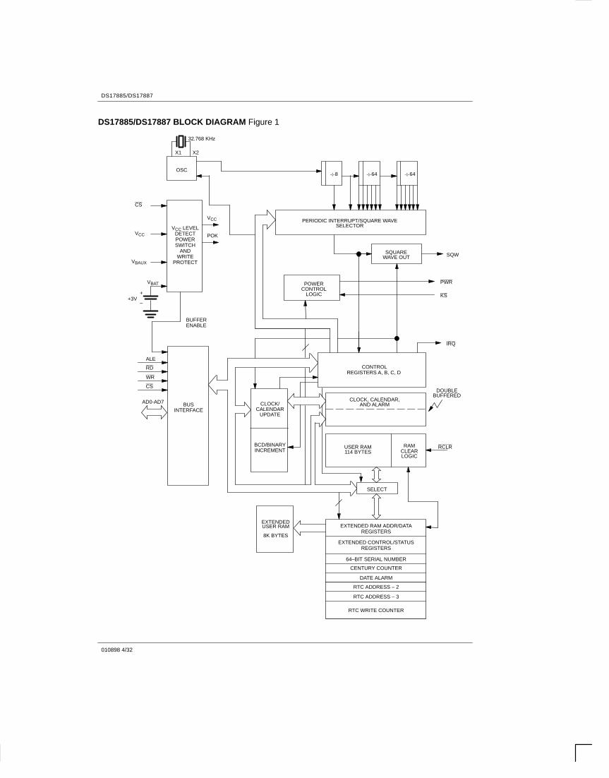
OPERATIONThe block diagram in Figure 1 shows the pin connec-tions with the major internal functions of theDS17885/DS17887. The following paragraphsdescribe the function of each pin.
SIGNAL DESCRIPTIONSGND, VCC – DC power is provided to the device onthese pins. VCC is the +3 volt or +5 volt input.
SQW (Square Wave Output) – The SQW pin will pro-vide a 32 KHz square wave output, tREC, after a pow-er–up condition has been detected. This condition setsthe following bits, enabling the 32 KHz output; DV1=1,and E32K=1. A square wave will be output on this pin ifeither SQWE=1 or E32K=1. If E32K=1, then 32 KHz willbe output regardless of the other control bits. If E32K=0,then the output frequency is dependent on the controlbits in register A. The SQW pin can output a signal fromone of 13 taps provided by the 15 internal divider stagesof the real time clock. The frequency of the SQW pin canbe changed by programming Register A as shown inTable 2. The SQW signal can be turned on and off usingthe SQWE bit in register B or the E32K bit in extendedregister 4Bh. A 32 KHz SQW signal is output when theEnable 32 KHz (E32K) bit in extended register 4Bh is alogic one, and VCC is above VPF. A 32 KHz square waveis also available when VCC is less than VPF if E32K=1,ABE=1, and voltage is applied to the VBAUX pin.
AD0–AD7 (Multiplexed Bidirectional Address/DataBus) – Multiplexed buses save pins because addressinformation and data information time share the samesignal paths. The addresses are present during the firstportion of the bus cycle and the same pins and signalpaths are used for data in the second portion of thecycle. Address/data multiplexing does not slow theaccess time of the DS17885 since the bus change fromaddress to data occurs during the internal RAM accesstime. Addresses must be valid prior to the latter portionof ALE, at which time the DS17885/DS17887 latchesthe address. Valid write data must be present and heldstable during the latter portion of the WR pulse. In a readcycle the DS17885/DS17887 outputs 8 bits of data dur-ing the latter portion of the RD pulse. The read cycle isterminated and the bus returns to a high impedancestate as RD transitions high. The address/data bus alsoserves as a bidirectional data path for the externalextended RAM.

DS17885/DS17887
010898 3/32
ALE (RTC Address Strobe Input; active high) – Apulse on the address strobe pin serves to demultiplexthe bus. The falling edge of ALE causes the RTCaddress to be latched within the DS17885/DS17887.
RD (RTC Read Input; active low) – RD identifies thetime period when the DS17885/DS17887 drives the buswith RTC read data. The RD signal is an enable signalfor the output buffers of the clock.
WR (RTC Write Input; active low) – The WR signal isan active low signal. The WR signal defines the timeperiod during which data is written to the addressed reg-ister.
CS (RTC Chip Select Input; active low) – The ChipSelect signal must be asserted low during a bus cyclefor DS17885/DS17887 to be accessed. CS must bekept in the active state during RD and WR timing. Buscycles which take place with ALE asserted but withoutasserting CS will latch addresses. However, no datatransfer will occur.
IRQ (Interrupt Request Output; open drain, activelow) – The IRQ pin is an active low output of theDS17885/DS17887 that can be tied to the interrupt inputof a processor. The IRQ output remains low as long asthe status bit causing the interrupt is present and thecorresponding interrupt–enable bit is set. To clear theIRQ pin, the application software must clear all enabledflag bits contributing to IRQ’s active state.
When no interrupt conditions are present, the IRQ levelis in the high impedance state. Multiple interruptingdevices can be connected to an IRQ bus. The IRQ pin
is an open drain output and requires an external pull–upresistor.
PWR (Power On Output; open drain, active low) –The PWR pin is intended for use as an on/off control forthe system power. With VCC voltage removed from theDS17885/DS17887, PWR may be automatically acti-vated from a Kickstart input via the KS pin or from aWake Up interrupt. Once the system is powered on, thestate of PWR can be controlled via bits in the Dallas reg-isters.
KS (Kickstart Input; active low) – When VCC isremoved from the DS17885/DS17887, the system canbe powered on in response to an active low transition onthe KS pin, as might be generated from a key closure.VBAUX must be present and Auxiliary Battery Enable bit(ABE) must be set to 1 if the kickstart function is used,and the KS pin must be pulled up to the VBAUX supply.While VCC is applied, the KS pin can be used as an inter-rupt input.
RCLR (RAM Clear Input; active low) – If enabled bysoftware, taking RCLR low will result in the clearing ofthe 114 bytes of user RAM. When enabled, RCLR canbe activated whether or not VCC is present.
VBAUX – Auxiliary battery input required for kickstartand wake up features. This input also supports clock/calendar and user RAM if VBAT is at lower voltage or isnot present. A standard +3 volt lithium cell or otherenergy source can be used. Battery voltage must be heldbetween +2.5 and +3.7 volts for proper operation. IfVBAUX is not going to be used it should be grounded andauxiliary battery enable bit bank 1, register 4BH,should=0.
DS17885/DS17887
010898 4/32
DS17885/DS17887 BLOCK DIAGRAM Figure 1
OSC
VCC
BUFFERENABLE
PERIODIC INTERRUPT/SQUARE WAVESELECTOR
SQUAREWAVE OUT SQW
IRQ
DOUBLEBUFFERED
REGISTERS A, B, C, D
CLOCK, CALENDAR,AND ALARM
BCD/BINARYINCREMENT
CLOCK/CALENDAR
UPDATE
BUSINTERFACE
ALE
RD
WR
AD0-AD7
X1 X2
VBAUX
VCC
CS
POK
+
–+3V
VBAT POWERCONTROL
LOGIC KS
PWR
CS
SELECT
USER RAM114 BYTES
RAMCLEARLOGIC
RCLR
EXTENDED CONTROL/STATUSREGISTERS
64–BIT SERIAL NUMBER
CENTURY COUNTER
DATE ALARM
�64�8 �64
CONTROL
VCC LEVELDETECTPOWERSWITCH
ANDWRITE
PROTECT
32.768 KHz
EXTENDED RAM ADDR/DATAREGISTERS
EXTENDEDUSER RAM
8K BYTES
RTC ADDRESS – 2
RTC ADDRESS – 3
RTC WRITE COUNTER

DS17885/DS17887
010898 5/32
DS17885 ONLYX1, X2 – Connections for a standard 32.768 KHz quartzcrystal. For greatest accuracy, the DS17885 must beused with a crystal that has a specified load capacitanceof either 6 pF or 12.5 pF. The Crystal Select (CS) bit inExtended Control Register 4B is used to select opera-tion with a 6 pF or 12.5 pF crystal. The crystal isattached directly to the X1 and X2 pins. There is noneed for external capacitors or resistors. Note: X1 andX2 are very high impedance nodes. It is recommendedthat they and the crystal be guard–ringed with groundand that high frequency signals be kept away from thecrystal area.
For more information on crystal selection and crystallayout considerations, please consult Application Note58, “Crystal Considerations with Dallas Real TimeClocks”. The DS17885 can also be driven by an exter-nal 32.768 KHz oscillator. In this configuration, the X1pin is connected to the external oscillator signal and theX2 pin is floated.
VBAT – Battery input for any standard 3 Volt lithium cellor other energy source. Battery voltage must be heldbetween 2.5 and 3.7 volts for proper operation.
POWER–DOWN/POWER–UPCONSIDERATIONSThe real–time clock function will continue to operate andall of the RAM, time, calendar, and alarm memory loca-tions remain nonvolatile regardless of the level of theVCC input. When VCC is applied to theDS17885/DS17887 and reaches a level of greater thanVPF (power fail trip point), the device becomes accessi-ble after tREC, provided that the oscillator is running andthe oscillator countdown chain is not in reset (see Regis-ter A). This time period allows the system to stabilizeafter power is applied.
The DS17885/DS17887 is available in either a 3 volt ora 5 volt device.
The 5 volt device is fully accessible and data can be writ-ten and read only when VCC is greater than 4.5 volts.When VCC is below 4.5 volts, read and writes are inhib-ited. However, the timekeeping function continuesunaffected by the lower input voltage. As VCC fallsbelow the greater of VBAT and VBAUX, the RAM andtimekeeper are switched over to a lithium battery con-nected either to the VBAT pin or VBAUX pin.
The 3 volt device is fully accessible and data can be writ-ten or read only when VCC is greater than 2.7 volts.When VCC falls below VPF, access to the device is inhib-ited. If VPF is less than VBAT and VBAUX, the power sup-ply is switched from VCC to the backup supply (thegreater of VBAT and VBAUX) when VCC drops below VPF.If VPF is greater than VBAT and VBAUX, the power supplyis switched from VCC to the backup supply when VCCdrops below the larger of VBAT and VBAUX.
When VCC falls below VPF, the chip is write-protected.With the possible exception of the KS, PWR, RCLR andSQW pins, all inputs are ignored and all outputs are in ahigh impedance state.
RTC ADDRESS MAPThe address map for the RTC registers of theDS17885/DS17887 is shown in Figure 2. The addressmap consists of the 14 clock/calendar registers. Tenregisters contain the time, calendar, and alarm data,and four bytes are used for control and status. All regis-ters can be directly written or read except for the follow-ing:
1. Registers C and D are read–only.
2. Bit–7 of Register A is read–only.
3. The high order bit of the seconds byte is read–only.

DS17885/DS17887
010898 6/32
DS17885 REAL TIME CLOCK ADDRESS MAP Figure 2
0 00H
13
14
0DH
0EH
0
1
2
3
4
5
6
7
8
9
10
11
12
13
SECONDS
SECONDS ALARM
MINUTES
MINUTES ALARM
HOURS
HOURS ALARM
DAY OF THE WEEK
DAY OF THE MONTH
MONTH
YEAR
REGISTER A
REGISTER B
REGISTER C
REGISTER D
BIN
AR
Y O
R B
CD
INP
UT
S
07FH127
CLOCK/CALENDAR14 BYTES
BANK 0,
63
64
03FH
040H
BANK 1REGISTERS,
RAM
50 BYTESUSER RAM
TIME, CALENDAR AND ALARM LOCATIONSThe time and calendar information is obtained by read-ing the appropriate register bytes shown in Table 1. Thetime, calendar, and alarm are set or initialized by writingthe appropriate register bytes. The contents of the time,calendar, and alarm registers can be either Binary orBinary–Coded Decimal (BCD) format. Table 1 showsthe binary and BCD formats of the twelve time, calendar,and alarm locations that reside in both bank 0 and inbank 1, plus the two extended registers that reside inbank 1 only (bank 0 and bank 1 switching will beexplained later in this text).
Before writing the internal time, calendar, and alarm reg-isters, the SET bit in Register B should be written to alogic one to prevent updates from occurring whileaccess is being attempted. Also at this time, the dataformat (binary or BCD), should be set via the data modebit (DM) of Register B. All time, calendar, and alarm reg-isters must use the same data mode. The set bit in Reg-ister B should be cleared after the data mode bit hasbeen written to allow the real–time clock to update thetime and calendar bytes.
Once initialized, the real–time clock makes all updatesin the selected mode. The data mode cannot bechanged without reinitializing the ten data bytes. The24/12 bit cannot be changed without reinitializing thehour locations. When the 12–hour format is selected,the high order bit of the hours byte represents PM when
it is a logic one. The time, calendar, and alarm bytes arealways accessible because they are double buffered.Once per second the ten bytes are advanced by onesecond and checked for an alarm condition. If a read ofthe time and calendar data occurs during an update, aproblem exists where seconds, minutes, hours, etc.may not correlate. The probability of reading incorrecttime and calendar data is low. Several methods ofavoiding any possible incorrect time and calendar readsare covered later in this text.
The four alarm bytes can be used in two ways. First,when the alarm time is written in the appropriate hours,minutes, and seconds alarm locations, the alarm inter-rupt is initiated at the specified time each day if the alarmenable bit is high . The second use condition is to inserta “don’t care” state in one or more of the four alarmbytes. The “don’t care” code is any hexadecimal valuefrom C0 to FF. The two most significant bits of each byteset the “don’t care” condition when at logic 1. An alarmwill be generated each hour when the “don’t care” bitsare set in the hours byte. Similarly, an alarm is gener-ated every minute with “don’t care” codes in the hoursand minute alarm bytes. The “don’t care” codes in allthree alarm bytes create an interrupt every second. Thethree alarm bytes may be used in conjunction with thedate alarm as described in the Wakeup/Kickstart sec-tion. The century counter will be discussed later in thistext.

DS17885/DS17887
010898 7/32
TIME, CALENDAR AND ALARM DATA MODES Table 1
ADDRESSLOCATION FUNCTION
DECIMALRANGE
RANGEADDRESSLOCATION FUNCTION
DECIMALRANGE BINARY DATA MODE BCD DATA MODE
00H Seconds 0–59 00–3B 00–59
01H Seconds Alarm 0–59 00–3B 00–59
02H Minutes 0–59 00–3B 00–59
03H Minutes Alarm 0–59 00–3B 00–59
04H Hours 12–hr. Mode 1–12 01-0C AM, 81-8C PM 01-12 AM, 81-92 PM
Hours 24–Hour Mode 0–23 00–17 00–23
05H Hours Alarm 12-hr. Mode 1–12 01-0C AM, 81-8C PM 01-12AM, 81-92 PM
Hours Alarm 24-hr. Mode 0–23 00–17 00–23
06H Day of Week Sunday=1 1–7 01–07 01–07
07H Date of Month 1–31 01–1F 01–31
08H Month 1–12 01–0C 01–12
09H Year 0–99 00–63 00–99
BANK 1, 48H Century 0–99 00–63 00–99
BANK 1, 49H Date Alarm 1–31 01–1F 01–31
CONTROL REGISTERSThe four control registers; A, B, C, and D reside in bothbank 0 and bank 1. These registers are accessible at alltimes, even during the update cycle.
NONVOLATILE RAM – RTCThe general purpose nonvolatile RAM bytes are notdedicated to any special function within theDS17885/DS17887. They can be used by the applica-tion program as nonvolatile memory and are fully avail-able during the update cycle.
The user RAM is divided into two separate memorybanks. When the bank 0 is selected, the 14 real timeclock registers and 114 bytes of user RAM are accessi-ble. When bank 1 is selected, an additional 8K bytes ofuser RAM are accessible through the extended RAMaddress and data registers.
INTERRUPT CONTROLThe DS17885/DS17887 includes six separate, fullyautomatic sources of interrupt for a processor:
1. Alarm interrupt
2. Periodic interrupt
3. Update–ended interrupt
4. Wake up interrupt
5. Kickstart interrupt
6. RAM clear interrupt
The conditions which generate each of these indepen-dent interrupt conditions are described in greater detailelsewhere in this data sheet. This section describes theoverall control of the interrupts.
The application software can select which interrupts, ifany, are to be used. There are a total of six bits includingthree bits in Register B and three bits in Extended Reg-ister B which enable the interrupts. The extended regis-ter locations are described later. Writing a logic 1 to aninterrupt enable bit permits that interrupt to be initiatedwhen the event occurs. A logic 0 in the interrupt enablebit prohibits the IRQ pin from being asserted from thatinterrupt condition. If an interrupt flag is already setwhen an interrupt is enabled, IRQ will immediately beset at an active level, even though the event initiating theinterrupt condition may have occurred much earlier. As
DS17885/DS17887
010898 8/32
a result, there are cases where the software shouldclear these earlier generated interrupts before firstenabling new interrupts.
When an interrupt event occurs, the relating flag bit isset to a logic 1 in Register C or in Extended Register A.These flag bits are set regardless of the setting of thecorresponding enable bit located either in Register B orin Extended Register B. The flag bits can be used in apolling mode without enabling the correspondingenable bits.
However, care should be taken when using the flag bitsof Register C as they are automatically cleared to 0immediately after they are read. Double latching isimplemented on these bits so that bits which are setremain stable throughout the read cycle. All bits whichwere set are cleared when read and new interruptswhich are pending during the read cycle are held untilafter the cycle is completed. One, two, or three bits canbe set when reading Register C. Each utilized flag bitshould be examined when read to ensure that no inter-rupts are lost.
The flag bits in Extended Register A are not automati-cally cleared following a read. Instead, each flag bit canbe cleared to 0 only by writing 0 to that bit.
When using the flag bits with fully enabled interrupts, theIRQ line will be driven low when an interrupt flag bit is setand its corresponding enable bit is also set. IRQ will beheld low as long as at least one of the six possible interruptsources has it s flag and enable bits both set. The IRQFbit in Register C is a 1 whenever the IRQ pin is beingdriven low as a result of one of the six possible activesources. Therefore, determination that theDS17885/DS17887 initiated an interrupt is accomplishedby reading Register C and finding IRQF=1. IRQF willremain set until all enabled interrupt flag bits are clearedto 0.
SQUARE WAVE OUTPUT SELECTIONThe SQW pin can be programmed to output a variety offrequencies divided down from the 32.768 KHz crystaltied to X1 and X2. The square wave output is enabledand disabled via the SQWE bit in Register B or the E32Kbit in extended register 4Bh. If the square wave isenabled (SQWE=1 or E32K=1), then the output fre-quency will be determined by the settings of the E32K bitin Extended Register 4Bh and by the RS3–0 bits in Reg-
ister A. If E32K=1, then a 32.768 KHz square wave willbe output on the SQW pin regardless of the settings ofRS3–0 and SQWE.
If E32K = 0, then the square wave output frequency isdetermined by the RS3-0 bits. These bits control a1–of–15 decoder which selects one of thirteen taps thatdivide the 32.768 KHz frequency. The RS3–0 bitsestablish the SQW output frequency as shown inTable 2. In addition, RS3–0 bits control the periodicinterrupt selection as described below.
If E32K=1, and the Auxiliary Battery Enable bit (ABE,bank 1; register 04BH) is enabled, and voltage isapplied to VBAUX then the 32 KHz square wave outputsignal will be output on the SQW pin in the absence ofVCC. This facility is provided to clock external powermanagement circuitry. If any of the above requirementsare not met, no square wave output signal will be gener-ated on the SQW pin in the absence of VCC.
A pattern of 01X in the DV2, DV1, and DV0, bits respec-tively, will turn the oscillator on and enable the count-down chain. Note that this is different than the DS1287,which required a pattern of 010 in these bits. DV0 is nowa “don’t care” because it is used for selection betweenregister banks 0 and 1.
A pattern of 11X will turn the oscillator on, but the oscilla-tor’s countdown chain will be held in reset, as it was inthe DS1287. Any other bit combination for DV2 andDV1 will keep the oscillator off.
PERIODIC INTERRUPT SELECTIONThe periodic interrupt will cause the IRQ pin to go to anactive state from once every 500 ms to once every122 µs. This function is separate from the alarm inter-rupt which can be output from once per second to onceper day. The periodic interrupt rate is selected using thesame RS3–0 bits in Register A which select the squarewave frequency (see Table 2). Changing the bits affectsboth the square wave frequency and the periodic inter-rupt output. However, each function has a separateenable bit in Register B. The SQWE and E32K bits con-trol the square wave output. Similarly, the periodic inter-rupt is enabled by the PIE bit in Register B. The periodicinterrupt can be used with software counters to measureinputs, create output intervals, or await the next neededsoftware function.

DS17885/DS17887
010898 9/32
UPDATE CYCLEThe Serialized RTC executes an update cycle once persecond regardless of the SET bit in Register B. Whenthe SET bit in Register B is set to one, the user copy ofthe double buffered time, calendar, alarm and elapsedtime byte is frozen and will not update as the time incre-ments. However, the time countdown chain continues toupdate the internal copy of the buffer. This featureallows the time to maintain accuracy independent ofreading or writing the time, calendar, and alarm buffersand also guarantees that time and calendar informationis consistent. The update cycle also compares eachalarm byte with the corresponding time byte and issuesan alarm if a match or if a “don’t care” code is present inall alarm locations.
There are three methods that can handle access of thereal–time clock that avoid any possibility of accessing
inconsistent time and calendar data. The first methoduses the update–ended interrupt. If enabled, an inter-rupt occurs after every up date cycle that indicates thatover 999 ms are available to read valid time and dateinformation. If this interrupt is used, the IRQF bit in Reg-ister C should be cleared before leaving the interruptroutine.
A second method uses the update–in–progress bit(UIP) in Register A to determine if the update cycle is inprogress. The UIP bit will pulse once per second. Afterthe UIP bit goes high, the update transfer occurs 244 µslater. If a low is read on the UIP bit, the user has at least244 µs before the time/calendar data will be changed.Therefore, the user should avoid interrupt service rou-tines that would cause the time needed to read validtime/calendar data to exceed 244 µs.
PERIODIC INTERRUPT RATE AND SQUARE WAVE OUTPUT FREQUENCY Table 2
EXT. REG. B SELECT BITS REGISTER A tPI PERIODIC SQW OUTPUT
E32K RS3 RS2 RS1 RS0
tPI PERIODICINTERRUPT RATE
SQW OUTPUTFREQUENCY
0 0 0 0 0 None None
0 0 0 0 1 3.90625 ms 256 Hz
0 0 0 1 0 7.8125 ms 128 Hz
0 0 0 1 1 122.070 µs 8.192 KHz
0 0 1 0 0 244.141 µs 4.096 KHz
0 0 1 0 1 488.281 µs 2.048 KHz
0 0 1 1 0 976.5625 µs 1.024 KHz
0 0 1 1 1 1.953125 ms 512 Hz
0 1 0 0 0 3.90625 ms 256 Hz
0 1 0 0 1 7.8125 ms 128 Hz
0 1 0 1 0 15.625 ms 64 Hz
0 1 0 1 1 31.25 ms 32 Hz
0 1 1 0 0 62.5 ms 16 Hz
0 1 1 0 1 125 ms 8 Hz
0 1 1 1 0 250 ms 4 Hz
0 1 1 1 1 500 ms 2 Hz
1 X X X X * 32.768 KHz
*RS3–RS0 determine periodic interrupt rates as listed for E32K=0.
DS17885/DS17887
010898 10/32
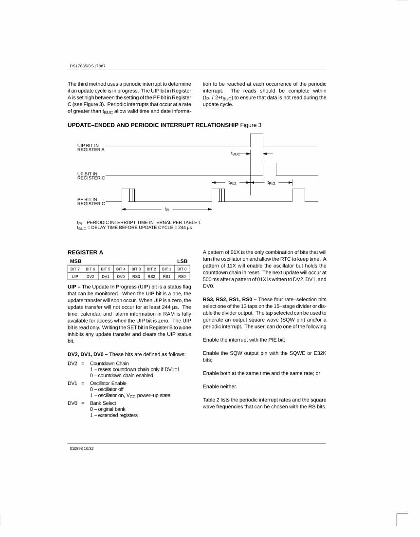
The third method uses a periodic interrupt to determineif an update cycle is in progress. The UIP bit in RegisterA is set high between the setting of the PF bit in RegisterC (see Figure 3). Periodic interrupts that occur at a rateof greater than tBUC allow valid time and date informa-
tion to be reached at each occurrence of the periodicinterrupt. The reads should be complete within(tPI / 2+tBUC) to ensure that data is not read during theupdate cycle.
UPDATE–ENDED AND PERIODIC INTERRUPT RELATIONSHIP Figure 3
ÎÎÎÎÎÎ
ÎÎÎÎÎÎ
tBUC
tPI/2tPI/2
tPI
UIP BIT INREGISTER A
UF BIT INREGISTER C
PF BIT INREGISTER C
tPI = PERIODIC INTERRUPT TIME INTERNAL PER TABLE 1tBUC = DELAY TIME BEFORE UPDATE CYCLE = 244 µs
REGISTER AMSB LSBBIT 7 BIT 6 BIT 5 BIT 4 BIT 3 BIT 2 BIT 1 BIT 0
UIP DV2 DV1 DV0 RS3 RS2 RS1 RS0
UIP – The Update In Progress (UIP) bit is a status flagthat can be monitored. When the UIP bit is a one, theupdate transfer will soon occur. When UIP is a zero, theupdate transfer will not occur for at least 244 µs. Thetime, calendar, and alarm information in RAM is fullyavailable for access when the UIP bit is zero. The UIPbit is read only. Writing the SET bit in Register B to a oneinhibits any update transfer and clears the UIP statusbit.
DV2, DV1, DV0 – These bits are defined as follows:
DV2 = Countdown Chain1 – resets countdown chain only if DV1=10 – countdown chain enabled
DV1 = Oscillator Enable0 – oscillator off1 – oscillator on, VCC power–up state
DV0 = Bank Select0 – original bank1 – extended registers
A pattern of 01X is the only combination of bits that willturn the oscillator on and allow the RTC to keep time. Apattern of 11X will enable the oscillator but holds thecountdown chain in reset. The next update will occur at500 ms after a pattern of 01X is written to DV2, DV1, andDV0.
RS3, RS2, RS1, RS0 – These four rate–selection bitsselect one of the 13 taps on the 15–stage divider or dis-able the divider output. The tap selected can be used togenerate an output square wave (SQW pin) and/or aperiodic interrupt. The user can do one of the following
Enable the interrupt with the PIE bit;
Enable the SQW output pin with the SQWE or E32Kbits;
Enable both at the same time and the same rate; or
Enable neither.
Table 2 lists the periodic interrupt rates and the squarewave frequencies that can be chosen with the RS bits.

DS17885/DS17887
010898 11/32
REGISTER BMSB LSBBIT 7 BIT 6 BIT 5 BIT 4 BIT 3 BIT 2 BIT 1 BIT 0
SET PIE AIE UIE SQWE DM 24/12 DSE
SET – When the SET bit is a zero, the update transferfunctions normally by advancing the counts once persecond. When the SET bit is written to a one, any updatetransfer is inhibited and the program can initialize thetime and calendar bytes without an update occurring inthe midst of initializing. Read cycles can be executed ina similar manner. SET is a read/write bit that is not modi-fied by internal functions of the DS17885/DS17887.
PIE – The Periodic Interrupt Enable bit is a read/write bitwhich allows the Periodic Interrupt Flag (PF) bit in Reg-ister C to drive the IRQ pin low. When the PIE bit is set toone, periodic interrupts are generated by driving theIRQ pin low at a rate specified by the RS3–RS0 bits ofRegister A. A zero in the PIE bit blocks the IRQ outputfrom being driven by a periodic interrupt, but the Peri-odic Flag (PF) bit is still set at the periodic rate. PIE is notmodified by any internal DS17885/DS17887 functions.
AIE – The Alarm Interrupt Enable (AIE) bit is a read/write bit which, when set to a one, permits the AlarmFlag (AF) bit in register C to assert IRQ. An alarm inter-rupt occurs for each second that the three time bytesequal the three alarm bytes including a “don’t care”alarm code of binary 11XXXXXX. When the AIE bit isset to zero, the AF bit does not initiate the IRQ signal.The internal functions of the DS17885/DS17887 do notaffect the AIE bit.
UIE – The Update Ended Interrupt Enable (UIE) bit is aread/write that enables the Update End Flag (UF) bit inRegister C to assert IRQ. The SET bit going high clearsthe UIE bit.
SQWE – When the Square Wave Enable (SQWE) bit isset to a one and E32K=0, a square wave signal at thefrequency set by the rate–selection bits RS3 throughRS0 is driven out on the SQW pin. When the SQWE bitis set to zero and E32K=0, the SQW pin is held low.SQWE is a read/write bit. SQWE is set to a one whenVCC is powered up.
DM – The Data Mode (DM) bit indicates whether timeand calendar information is in binary or BCD format.The DM bit is set by the program to the appropriate for-mat and can be read as required. This bit is not modified
by internal functions. A one in DM signifies binary datawhile a zero in DM specifies Binary Coded Decimal(BCD) data.
24/12 – The 24/12 control bit establishes the format ofthe hours byte. A one indicates the 24–hour mode and azero indicates the 12–hour mode. This bit is read/write.
DSE – The Daylight Savings Enable (DSE) bit is a read/write bit which enables two special updates when DSEis set to one. On the first Sunday in April the time incre-ments from 1:59:59 AM to 3:00:00 AM. On the lastSunday in October when the time first reaches 1:59:59AM it changes to 1:00:00 AM. These special updates donot occur when the DSE bit is a zero. This bit is notaffected by internal functions.
REGISTER CMSB LSBBIT 7 BIT 6 BIT 5 BIT 4 BIT 3 BIT 2 BIT 1 BIT 0
IRQF PF AF UF 0 0 0 0
IRQF – The Interrupt Request Flag (IRQF) bit is set to aone when one or more of the following are true:
PF = PIE = 1 WF = WIE = 1AF = AIE = 1 KF = KSE= 1UF = UIE = 1 RF = RIE = 1
i.e., IRQF = (PF • PIE) + (AF • AIE) + (UF • UIE) +(WF • WIE) + (KF • KSE) + (RF • RIE)
Any time the IRQF bit is a one, the IRQ pin is driven low.Flag bits PF, AF, and UF are cleared after Register C isread by the program.
PF – The Periodic Interrupt Flag (PF) is a read–only bitwhich is set to a one when an edge is detected on theselected tap of the divider chain. The RS3 through RS0bits establish the periodic rate. PF is set to a one inde-pendent of the state of the PIE bit. When both PF andPIE are ones, the IRQ signal is active and will set theIRQF bit. The PF bit is cleared by a software read ofRegister C.
AF – A one in the Alarm Interrupt Flag (AF) bit indicatesthat the current time has matched the alarm time. If theAIE bit is also a one, the IRQ pin will go low and a one willappear in the IRQF bit. A read of Register C willclear AF.

DS17885/DS17887
010898 12/32
UF – The Update Ended Interrupt Flag (UF) bit is setafter each update cycle. When the UIE bit is set to one,the one in UF causes the IRQF bit to be a one which willassert the IRQ pin. UF is cleared by reading Register C.
BIT 3 THROUGH BIT 0 – These are unused bits of thestatus Register C. These bits always read zero and can-not be written.
REGISTER DMSB LSBBIT 7 BIT 6 BIT 5 BIT 4 BIT 3 BIT 2 BIT 1 BIT 0
VRT 0 0 0 0 0 0 0
VRT – The Valid RAM and Time (VRT) bit indicates thecondition of the battery connected to the VBAT pin or thebattery connected to VBAUX, whichever is at a highervoltage. This bit is not writable and should always be aone when read. If a zero is ever present, an exhaustedlithium energy source is indicated and both the contentsof the RTC data and RAM data are questionable.
BIT 6 THROUGH BIT 0 – The remaining bits of RegisterD are not usable. They cannot be written and, whenread, they will always read zero.
EXTENDED FUNCTIONSThe extended functions provided by theDS17885/DS17887 that are new to the RAMified RTCfamily are accessed via a software controlled bankswitching scheme, as illustrated in Figure 4. In bank 0,the clock/calendar registers and 50 bytes of user RAM
are in the same locations as for the DS1287. As a result,existing routines implemented within BIOS, DOS, orapplication software packages can gain access to theDS17885/DS17887 clock registers with no changes.Also in bank 0, an extra 64 bytes of RAM are provided ataddresses just above the original locations for a total of114 directly addressable bytes of user RAM.
When bank 1 is selected, the clock/calendar registersand the original 50 bytes of user RAM still appear asbank 0. However, the Dallas registers which providecontrol and status for the extended functions will beaccessed in place of the additional 64 bytes of userRAM. The major extended functions controlled by theDallas registers are listed below:
1. 64–bit Silicon Serial Number
2. Century counter
3. Date Alarm
4. Auxiliary Battery Control/Status
5. Wake Up
6. Kickstart
7. RAM Clear Control/Status
8. 8K bytes Extended RAM Access
The bank selection is controlled by the state of the DV0bit in register A. To access bank 0 the DV0 bit should bewritten to a 0. To access bank 1, DV0 should be writtento a 1. Register locations designated as reserved in thebank 1 map are reserved for future use by Dallas Semi-conductor. Bits in these locations cannot be written andwill return a 0 if read.

DS17885/DS17887
010898 13/32
DS17885/DS17887 EXTENDED REGISTER BANK DEFINITION Figure 4
RESERVED
RESERVED
RESERVED
RESERVED
RESERVED
RESERVED
RESERVED
RESERVED
RESERVED
RESERVED
00
OD0E
3F
40
41
42
43
44
45
46
47
48
49
4A
4B
4C
4D
4E
4F
50
51
52
53
54
7F
DV0 = 100
OD0E
3F
7F
DV0 = 0BANK 0 BANK 1
TIMEKEEPING AND CONTROL
50 BYTES–USER RAM
64 BYTES–USER RAM
TIMEKEEPING AND CONTROL
50 BYTES–USER RAM
MODEL NUMBER BYTE
1ST BYTE SERIAL NUMBER
2ND BYTE SERIAL NUMBER
3RD BYTE SERIAL NUMBER
4TH BYTE SERIAL NUMBER
5TH BYTE SERIAL NUMBER
6TH BYTE SERIAL NUMBER
CRC BYTE
CENTURY BYTE
DATE ALARM
EXTENDED CONTROL REG 4A
EXTENDED CONTROL REG 4B
RESERVED
RESERVED
RTC ADDRESS – 2
RTC ADDRESS – 3
EXTENDED RAM ADDR–LSB
EXTENDED RAM ADDR–MSB
RESERVED
EXTENDED RAM DATA PORT
MSB LSB MSB LSB
55
56
57
58
59
5A
5B
5C
5D
5F
67RESERVED
RESERVED
5E RTC WRITE COUNTER
EXTENDEDRAM
8K X 8

DS17885/DS17887
010898 14/32
SILICON SERIAL NUMBERA unique 64–bit lasered serial number is located in bank1, registers 40h – 47h. This serial number is divided intothree parts. The first byte in register 40h contains amodel number to identify the device type and revision ofthe DS17885/DS17887. Registers 41h – 46h contain aunique binary number. Register 47h contains a CRCbyte used to validate the data in registers 40h – 46h. Alleight bytes of the serial number are read–only registers.
The DS17885/DS17887 is manufactured such that notwo devices will contain an identical number in locations41h – 47h.
CENTURY COUNTERA register has been added in bank 1, location 48H, tokeep track of centuries. The value is read in eitherbinary or BCD according to the setting of the DM bit.
RTC WRITE COUNTERAn eight bit counter located in extended register bank 1,5Eh, will count the number of times the RTC is written to.This counter will be incremented on the rising edge ofthe WR signal every time that the CS signal qualifies it.This counter is a read–only register and will roll–overafter 256 RTC write pulses. This counter can be used todetermine if and how many RTC writes have occurredsince the last time this register was read.
8K X 8 EXTENDED RAMThe DS17885/DS17887 provides 8K x 8 of on–chipSRAM which is controlled as nonvolatile storage sus-tained from a lithium battery. On power–up, the RAM istaken out of write protect status by the internal powerOK signal (POK) generated from the write protect cir-cuitry.
The on–chip 8K x 8 nonvolatile SRAM is accessed viathe eight multiplexed address/data lines AD7 to AD0.Access to the SRAM is controlled by three on–chip latchregisters. Two registers are used to hold the SRAMaddress, and the other register is used to hold read/writedata. The SRAM address space is from 00h to 01FFFh.
Access to the extended 8K x 8 RAM is controlled viathree of the Dallas registers shown in Figure 4. The Dal-las registers in bank 1 must first be selected by settingthe DV0 bit in register A to a logic 1. The 12–bit addressof the RAM location to be accessed must be loaded intothe extended RAM address registers located at 50h and
51h. The least significant address byte should be writ-ten to location 50h, and the most significant 5–bits(right–justified) should be loaded in location 51h. Datain the addressed location may be read by performing aread operation from location 53h, or written to by per-forming a write operation to location 53h. Data in anyaddressed location may be read or written repeatedlywithout changing the address in location 50h and 51h.
To read or write consecutive extended RAM locations, aburst mode feature can be enabled to increment theextended RAM address. To enable the burst mode fea-ture, set the BME bit in the extended control register4Ah, to a logic 1. With burst mode enabled, write theextended RAM starting address location to registers50h and 51h. Then read or write the extended RAM datafrom/to register 53h. The extended RAM address loca-tions are automatically incremented on the rising edgeof RD or WR only when register 53h is being accessed.Refer to the Burst Mode Timing Waveform.
AUXILIARY BATTERYThe VBAUX input is provided to supply power from anauxiliary battery for the DS17885/DS17887 kickstart,wake up, and SQW output features in the absence ofVCC. This power source must be available in order touse these auxiliary features when no VCC is applied tothe device.
The Auxiliary Battery Enable (ABE; bank 1, register04BH) bit in extended control register B is used to turnon and off the auxiliary battery for the above functions inthe absence of VCC. When set to a 1, VBAUX batterypower is enabled, and when cleared to 0, VBAUX batterypower is disabled to these functions.
In the DS17885/DS17887, this auxiliary battery may beused as the primary backup power source for maintain-ing the clock/calendar, user RAM, and extended exter-nal RAM functions. This occurs if the VBAT pin is at alower voltage than VBAUX. If the DS17885 is to bebacked–up using a single battery with the auxiliary fea-tures enabled, then VBAUX should be used and VBATshould be grounded. If VBAUX is not to be used, it shouldbe grounded and ABE should be cleared to 0.
WAKE UP/KICKSTARTThe DS17885/DS17887 incorporates a wake up featurewhich can power the system on at a pre–determineddate through activation of the PWR output pin. In addi-

DS17885/DS17887
010898 15/32
tion, the kickstart feature can allow the system to bepowered up in response to a low going transition on theKS pin, without operating voltage applied to the VCC pin.As a result, system power may be applied upon suchevents as a key closure, or modem ring detect signal. Inorder to use either the wake up or the kickstart features,the DS17885/DS17887 must have an auxiliary batteryconnected to the VBAUX pin and the oscillator must berunning and the countdown chain must not be in reset(Register A DV2, DV1, DV0 = 01X). If DV2, DV1, andDV0 are not in this required state, the PWR pin will notbe driven low in response to a kickstart or wakeup condi-tion, while in battery–backed mode.
The wake up feature is controlled through the Wake upInterrupt Enable bit in extended control register B (WIE,bank 1, 04BH). Setting WIE to 1 enables the wake upfeature, clearing WIE to 0 disables it. Similarly, the kick-start feature is controlled through the Kickstart InterruptEnable bit in extended control register B (KSE, bank 1,04BH).
A wake up sequence will occur as follows: When wakeup is enabled via WIE = 1 while the system is powereddown (no VCC voltage), the clock/calendar will monitorthe current date for a match condition with the datealarm register (bank 1, register 049H). In conjunctionwith the date alarm register, the hours, minutes, andseconds alarm bytes in the clock/calendar register map(bank 0, registers 05H, 03H, and 01H) are also moni-tored. As a result, a wake up will occur at the date andtime specified by the date, hours, minutes, and secondsalarm register values. This additional alarm will occurregardless of the programming of the AIE bit (bank 0,register B, 0BH). When the match condition occurs, thePWR pin will automatically be driven low. This outputcan be used to turn on the main system power supplywhich provides VCC voltage to the DS17885/DS17887as well as the other major components in the system.Also at this time, the Wake Up flag (WF, bank 1, register04AH) will be set, indicating that a wake up conditionhas occurred.
A kickstart sequence will occur when kickstarting isenabled via KSE = 1. While the system is powereddown, the KS input pin will be monitored for a low goingtransition of minimum pulse width tKSPW. When such atransition is detected, the PWR line will be pulled low, asit is for a wake up condition. Also at this time, the Kick-start Flag (KF, bank 1, register 04AH) will be set, indicat-ing that a kickstart condition has occurred.
The timing associated with both the wake up and kick-starting sequences is illustrated in the Wake Up / Kick-start Timing Diagram in the Electrical Specificationssection of this data sheet. The timing associated withthese functions is divided into 5 intervals, labeled 1-5 onthe diagram.
The occurrence of either a kickstart or wake up condi-tion will cause the PWR pin to be driven low, asdescribed above. During interval 1, if the supply voltageon the DS17885/DS17887 VCC pin rises above the 3volt power fail level before the power on timeout period(tPOTO) expires, then PWR will remain at the active lowlevel. If VCC does not rise above the 3 volt power failvoltage in this time, then the PWR output pin will beturned off and will return to its high impedance level. Inthis event, the IRQ pin will also remain tri–stated. Theinterrupt flag bit (either WF or KF) associated with theattempted power on sequence will remain set untilcleared by software during a subsequent systempower on.
If VCC is applied within the timeout period, then the sys-tem power on sequence will continue as shown in inter-vals 2–5 in the timing diagram. During interval 2, PWRwill remain active and IRQ will be driven to its active lowlevel, indicating that either WF or KF was set in initiatingthe power on. In the diagram KS is assumed to be pulledup to the VBAUX supply. Also at this time, the PAB bit willbe automatically cleared to 0 in response to a success-ful power on. The PWR line will remain active as long asthe PAB remains cleared to 0.
At the beginning of interval 3, the system processor hasbegun code execution and clears the interrupt conditionof WF and/or KF by writing zeroes to both of these con-trol bits. As long as no other interrupt within theDS17885/DS17887 is pending, the IRQ line will betaken inactive once these bits are reset. Execution ofthe application software may proceed. During this time,both the wake up and kickstart functions may be used togenerate status and interrupts. WF will be set inresponse to a date, hours, minutes, and seconds matchcondition. KF will be set in response to a low going tran-sition on KS. If the associated interrupt enable bit is set(WIE and/or KSE) then the IRQ line will driven active lowin response to enabled event. In addition, the other pos-sible interrupt sources within the DS17885/DS17887may cause IRQ to be driven low. While system power isapplied, the on chip logic will always attempt to drive thePWR pin active in response to the enabled kickstart orwake up condition. This is true even if PWR was pre-

DS17885/DS17887
010898 16/32
viously inactive as the result of power being applied bysome means other than wake up or kickstart.
The system may be powered down under software con-trol by setting the PAB bit to a logic 1. This causes theopen-drain PWR pin to be placed in a high impedancestate, as shown at the beginning of interval 4 in the tim-ing diagram. As VCC voltage decays, the IRQ output pinwill be placed in a high impedance state when VCC goesbelow VPF. If the system is to be again powered on inresponse to a wake up or kickstart, then the both the WFand KF flags should be cleared and WIE and/or KSEshould be enabled prior to setting the PAB bit.
During interval 5, the system is fully powered down.Battery backup of the clock calendar and nonvolatileRAM is in effect and IRQ is tri–stated, and monitoring ofwake up and kickstart takes place. If PRS=1, PWRstays active, otherwise if PRS=0 PWR is tri–stated.
RAM CLEARThe DS17885/DS17887 provides a RAM clear functionfor the 114 bytes of user RAM. When enabled, this func-tion can be performed regardless of the condition of theVCC pin.
The RAM clear function is enabled or disabled via theRAM Clear Enable bit (RCE; bank 1, register 04BH).When this bit is set to a logic 1, the 114 bytes of userRAM will be cleared (all bits set to 1) when an active lowtransition is sensed on the RCLR pin. This action willhave no effect on either the clock/calendar settings orupon the contents of the extended RAM. The RAM clearFlag (RF, bank 1, register 04AH) will be set when theRAM clear operation has been completed. If VCC ispresent at the time of the RAM clear and RIE=1, the IRQline will also be driven low upon completion. The inter-rupt condition can be cleared by writing a zero to the RFbit. The IRQ line will then return to its inactive high levelprovided there are no other pending interrupts. Oncethe RCLR pin is activated, all read/write accesses arelocked out for a minimum recover time, specified astREC in the Electrical Characteristics section.
When RCE is cleared to zero, the RAM clear function isdisabled. The state of the RCLR pin will have no effecton the contents of the user RAM, and transitions on theRCLR pin have no effect on RF.
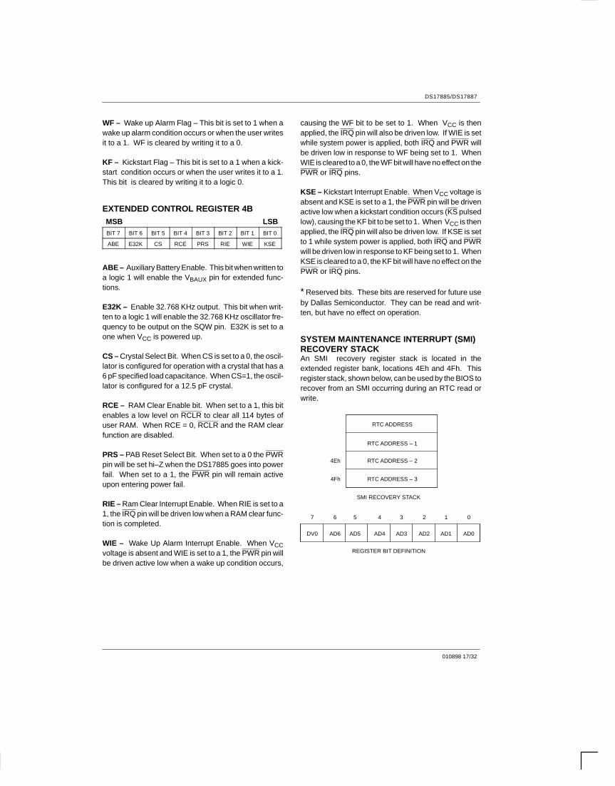
EXTENDED CONTROL REGISTERSTwo extended control registers are provided to supplycontrols and status information for the extended fea-tures offered by the DS17885/DS17887. These aredesignated as extended control registers A and B andare located in register bank 1, locations 04AH and04BH, respectively. The functions of the bits withinthese registers are described as follows.
EXTENDED CONTROL REGISTER 4AMSB LSBBIT 7 BIT 6 BIT 5 BIT 4 BIT 3 BIT 2 BIT 1 BIT 0
VRT2 INCR BME * PAB RF WF KF
VRT2 – This status bit gives the condition of the auxil-iary battery. It is set to a logic 1 condition when the exter-nal lithium battery is connected to the VBAUX. If this bit isread as a logic 0, the external battery should bereplaced.
INCR – Increment in Progress status bit. This bit is setto a 1 when an increment to the time/date registers is inprogress and the alarm checks are being made. INCRwill be set to a 1 at 122 µs before the update cycle startsand will be cleared to 0 at the end of each update cycle.
BME – Burst Mode Enable. The burst mode enable bitallows the extended user RAM address registers toautomatically increment for consecutive reads andwrites. When BME is set to a logic one, the automaticincrementing will be enabled and when BME is set to alogic zero, the automatic incrementing will be disabled.
PAB – Power Active Bar control bit. When this bit is 0,the PWR pin is in the active low state. When this bit is 1,the PWR pin is in the high impedance state. This bit canbe written to a logic 1 or 0 by the user. If either WF ANDWIE = 1 OR KF AND KSE = 1, the PAB bit will be clearedto 0.
RF – Ram Clear Flag. This bit will be set to a logic 1when a high to low transition occurs on the RCLR input ifRCE=1. The RF bit is cleared by writing it to a logic 0.This bit can also be written to a logic 1 to force an inter-rupt condition.
DS17885/DS17887
010898 17/32
WF – Wake up Alarm Flag – This bit is set to 1 when awake up alarm condition occurs or when the user writesit to a 1. WF is cleared by writing it to a 0.
KF – Kickstart Flag – This bit is set to a 1 when a kick-start condition occurs or when the user writes it to a 1.This bit is cleared by writing it to a logic 0.
EXTENDED CONTROL REGISTER 4BMSB LSBBIT 7 BIT 6 BIT 5 BIT 4 BIT 3 BIT 2 BIT 1 BIT 0
ABE E32K CS RCE PRS RIE WIE KSE
ABE – Auxiliary Battery Enable. This bit when written toa logic 1 will enable the VBAUX pin for extended func-tions.
E32K – Enable 32.768 KHz output. This bit when writ-ten to a logic 1 will enable the 32.768 KHz oscillator fre-quency to be output on the SQW pin. E32K is set to aone when VCC is powered up.
CS – Crystal Select Bit. When CS is set to a 0, the oscil-lator is configured for operation with a crystal that has a6 pF specified load capacitance. When CS=1, the oscil-lator is configured for a 12.5 pF crystal.
RCE – RAM Clear Enable bit. When set to a 1, this bitenables a low level on RCLR to clear all 114 bytes ofuser RAM. When RCE = 0, RCLR and the RAM clearfunction are disabled.
PRS – PAB Reset Select Bit. When set to a 0 the PWRpin will be set hi–Z when the DS17885 goes into powerfail. When set to a 1, the PWR pin will remain activeupon entering power fail.
RIE – Ram Clear Interrupt Enable. When RIE is set to a1, the IRQ pin will be driven low when a RAM clear func-tion is completed.
WIE – Wake Up Alarm Interrupt Enable. When VCCvoltage is absent and WIE is set to a 1, the PWR pin willbe driven active low when a wake up condition occurs,
causing the WF bit to be set to 1. When VCC is thenapplied, the IRQ pin will also be driven low. If WIE is setwhile system power is applied, both IRQ and PWR willbe driven low in response to WF being set to 1. WhenWIE is cleared to a 0, the WF bit will have no effect on thePWR or IRQ pins.
KSE – Kickstart Interrupt Enable. When VCC voltage isabsent and KSE is set to a 1, the PWR pin will be drivenactive low when a kickstart condition occurs (KS pulsedlow), causing the KF bit to be set to 1. When VCC is thenapplied, the IRQ pin will also be driven low. If KSE is setto 1 while system power is applied, both IRQ and PWRwill be driven low in response to KF being set to 1. WhenKSE is cleared to a 0, the KF bit will have no effect on thePWR or IRQ pins.
* Reserved bits. These bits are reserved for future useby Dallas Semiconductor. They can be read and writ-ten, but have no effect on operation.
SYSTEM MAINTENANCE INTERRUPT (SMI)RECOVERY STACKAn SMI recovery register stack is located in theextended register bank, locations 4Eh and 4Fh. Thisregister stack, shown below, can be used by the BIOS torecover from an SMI occurring during an RTC read orwrite.
RTC ADDRESS
RTC ADDRESS – 1
RTC ADDRESS – 2
RTC ADDRESS – 3
4Eh
4Fh
SMI RECOVERY STACK
DV0 AD6 AD0AD5 AD4 AD3 AD2 AD1
REGISTER BIT DEFINITION
7 6 5 4 3 2 1 0

DS17885/DS17887
010898 18/32
The RTC address is latched on the falling edge of theALE signal. Each time an RTC address is latched, theregister address stack is pushed. The stack is only fourregisters deep, holding the three previous RTC
addresses in addition to the current RTC address beingaccessed. The following waveform illustrates how theBIOS could recover the RTC address when an SMIoccurs.
1 2 3 4
ALE
1. The RTC address is latched.
2. An SMI is generated before an RTC read or write occurs.
3. RTC address 0Ah is latched and the address from “1” is pushed to the “RTC Address – 1” stack location. Thisstep is necessary to change the bank select bit, DV0=1.
4. RTC address 4Eh is latched and the address from “1” is pushed to location 4Eh, “RTC Address – 2” while 0Ah ispushed to the “RTC Address – 1” location. The data in this register, 4Eh, is the RTC address lost due to the SMI.

DS17885/DS17887
010898 19/32
ABSOLUTE MAXIMUM RATINGS*Voltage on Any Pin Relative to Ground –0.3V to +7.0VOperating Temperature 0°C to 70°CStorage Temperature DS17885 –55°C to +125°CStorage Temperature DS17887 –40°C to +70°CSoldering Temperature 260°C for 10 seconds (See Note 13)
* This is a stress rating only and functional operation of the device at these or any other conditions above thoseindicated in the operation sections of this specification is not implied. Exposure to absolute maximum ratingconditions for extended periods of time may affect reliability.
RECOMMENDED DC OPERATING CONDITIONS (0°C to 70°C)
PARAMETER SYMBOL MIN TYP MAX UNITS NOTES
Power Supply Voltage 5 VoltOperation
VCC 4.5 5.0 5.5 V 1
Power Supply Voltage 3 VoltOperation
VCC 2.7 3.0 3.3 V 1
Input Logic 1 VIH 2.3 VCC+0.3 V 1
Input Logic 0 VIL -0.3 0.6 V 1
Battery Voltage VBAT 2.5 3.7 V 1
Auxiliary Battery Voltage;VCC=5.0V
VBAUX 2.5 5.2 V 1
Auxiliary Battery Voltage;VCC=3.0V
VBAUX 2.5 3.7 V 1
DC ELECTRICAL CHARACTERISTICS (0°C to 70°C; VCC=5.0V ± 10%)
PARAMETER SYMBOL MIN TYP MAX UNITS NOTES
Average VCC Power SupplyCurrent
ICC1 25 50 mA 2, 3
CMOS Standby Current(CS=VCC–0.2V)
ICC2 1 3 mA 2, 3
Input Leakage Current (any input) IIL –1 +1 µA
Output Leakage Current IOL –1 +1 µA 6
Output Logic 1 Voltage(IOUT = –1.0 mA)
VOH 2.4 V
Output Logic 0 Voltage(IOUT = +2.1 mA)
VOL 0.4 V
Power Fail Trip Point VPF 4.25 4.37 4.5 V 4
Battery Switch Voltage VSW VBAT, VBAUX V 9

DS17885/DS17887
010898 20/32
DC ELECTRICAL CHARACTERISTICS (cont’d) (0°C to 70°C; VCC=5.0V ± 10%)
PARAMETER SYMBOL MIN TYP MAX UNITS NOTES
Battery Leakage OSC ON IBAT1 0.50 0.7 µA 12
Battery Leakage OSC OFF IBAT2 0.050 0.4 µA 12
I/O Leakage ILO –1 +1 µA 5
PWR Output @ 0.4V IOLPWR 10.0 mA 1
IRQ Output @ 0.4V IOLIRQ 2.1 mA 1
DC ELECTRICAL CHARACTERISTICS (0°C to 70°C; VCC=3.0V ± 10%)
PARAMETER SYMBOL MIN TYP MAX UNITS NOTES
Average VCC Power Supply Current ICC1 15 30 mA 2, 3
CMOS Standby Current(CS=VCC-0.2)
ICC2 0.5 2 mA 2, 3
Input Leakage Current (any input) IIL –1 +1 µA
Output Leakage Current IOL –1 +1 µA 6
Output Logic 1 Voltage@ –0.4 mA
VOH 2.4 V
Output Logic 0 Voltage@ +0.8 mA
VOL 0.4 V
Power Fail Trip Point VPF 2.5 2.6 2.7 V 4
Battery Leakage OSC ON IBAT1 0.50 0.7 µA 12
Battery Leakage OSC OFF IBAT2 0.050 0.4 µA 12
I/O Leakage ILO –1 +1 µA 5
PWR Output @ 0.4V IOLPWR 4 mA 1
IRQ Output @ 0.4V IOLIRQ 0.8 mA 1

DS17885/DS17887
010898 21/32
RTC AC TIMING CHARACTERISTICS (0°C to 70°C; VCC = 3.0V ± 10%)
PARAMETER SYMBOL MIN TYP MAX UNITS NOTES
Cycle Time tCYC 360 DC ns
Pulse Width, RD/WR Low PWRWL 200 ns
Pulse Width, RD/WR High PWRWH 150 ns
Input Rise and Fall Time tR, tF 30 ns
Chip Select Setup Time BeforeWR, or RD
tCS 20 ns
Chip Select Hold Time tCH 0 ns
Read Data Hold Time tDHR 10 90 ns
Write Data Hold Time tDHW 0 ns
Muxed Address Valid Time to ALEFall
tASL 40 ns
Muxed Address Hold Time fromALE fall
tAHL 10 ns
RD or WR High Setup to ALE Rise tASD 30 ns
Pulse Width ALE High PWASH 40 ns
ALE Low Setup to RD or WR Fall tASED 30 ns
Output Data Delay Time from RD tDDR 20 200 ns 7
Data Setup Time tDSW 60 ns
IRQ Release from RD tIRD 2 µs
AC TEST CONDITIONSOutput Load: 50 pFInput Pulse Levels: 0–3.0VTiming Measurement Reference Levels
Input: 1.5VOutput: 1.5V
Input Pulse Rise and Fall Times: 5 ns

DS17885/DS17887
010898 22/32
DS17885/DS17887 BUS TIMING FOR READ CYCLE TO RTC
tCYC
PWRWL
PWASH
tASDtASED
tASD
PWRWH
tCS
tCH
tDHRtAHL
tASL
ALE
WR
RD
CS
AD0–AD7
tDDR
IRQ
tIRD

DS17885/DS17887
010898 23/32
RTC AC TIMING CHARACTERISTICS (0°C to 70°C; VCC = 5.0V ± 10%)
PARAMETER SYMBOL MIN TYP MAX UNITS NOTES
Cycle Time tCYC 240 DC ns
Pulse Width, RD/WR Low PWRWL 120 ns
Pulse Width, RD/WR High PWRWH 80 ns
Input Rise and Fall Time tR, tF 30 ns
Chip Select Setup Time BeforeWR, or RD
tCS 20 ns
Chip Select Hold Time tCH 0 ns
Read Data Hold Time tDHR 10 50 ns
Write Data Hold Time tDHW 0 ns
Muxed Address Valid Time to ALEFall
tASL 20 ns
Muxed Address Hold Time fromALE fall
tAHL 10 ns
RD or WR High Setup to ALERise
tASD 25 ns
Pulse Width ALE High PWASH 40 ns
ALE Low Setup to RD or WR Fall tASED 30 ns
Output Data Delay Time from RD tDDR 20 120 ns 7
Data Setup Time tDSW 30 ns
IRQ Release from RD tIRD 2 µs
DS17885/DS17887 BUS TIMING FOR WRITE CYCLE TO RTC AND RTC REGISTERS
tCYC
PWRWL
PWASH
tASDtASED
tASD
PWRWH
tCS tDSW
tCH
tDHWtAHL
tASL
ALE
WR
RD
CS
AD0–AD7

DS17885/DS17887
010898 24/32
POWER–UP CONDITION 3 VOLT DEVICE
POWER FAIL
CS
VCC
VIH
tREC
3.0V2.7V
2.5V
tR
POWER–DOWN CONDITION 3 VOLT DEVICE
ÉÉÉÉÉÉÉÉÉÉÉÉÉÉÉÉÉÉÉÉÉ
VIH
tPF
tF
3.0V
2.7V
2.5V
POWER FAIL
CS
VCC
DS17885/DS17887
010898 25/32
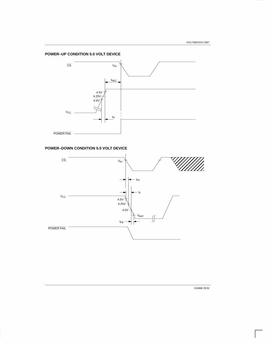
POWER–UP CONDITION 5.0 VOLT DEVICE
POWER FAIL
CS
VCC
VIH
tREC
4.5V4.25V
4.0V
tR
POWER–DOWN CONDITION 5.0 VOLT DEVICE
ÉÉÉÉÉÉÉÉÉÉÉÉÉÉÉÉÉÉ
VIH
tPF
tF
tFB
VBAT
4.5V
4.25V
4.0V
POWER FAIL
CS
VCC

DS17885/DS17887
010898 26/32
POWER–UP POWER–DOWN TIMING 5 VOLT DEVICE (tA = 25°C)
PARAMETER SYMBOL MIN TYP MAX UNITS NOTES
CS High to Power Fail tPF 0 ns
Recovery at Power–up tREC 150 ms
VCC Slew Rate Power–down tF4.0 <VCC < 4.5V
300 µs
VCC Slew Rate Power–down tFB3.0 <VCC< 4.0V
10 µs
VCC Slew Rate Power–up tR4.5V>VCC>4.0V
0 µs
Expected Data Retention tDR 10 years 10, 11
POWER–UP POWER–DOWN TIMING 3 VOLT DEVICE (tA = 25°C)
PARAMETER SYMBOL MIN TYP MAX UNITS NOTES
CS High to Power Fail tPF 0 ns
Recovery at Power–up tREC 150 ms
VCC Slew Rate Power–down tF2.5 <VCC < 3.0V
300 µs
VCC Slew Rate Power–up tR3.0V>VCC>2.5V
0 µs
Expected Data Retention tDR 10 years 10, 11
WARNING:Under no circumstances are negative undershoots, of any amplitude, allowed when device is in battery back–upmode.
CAPACITANCE (tA = 25°C)
PARAMETER SYMBOL MIN TYP MAX UNITS NOTES
Input Capacitance CIN 12 pF
Output Capacitance COUT 12 pF
WAKE UP/KICKSTART TIMING (tA = 25°C)
PARAMETER SYMBOL MIN TYP MAX UNITS NOTES
Kickstart Input Pulse Width tKSPW 2 µs
Wake up/Kickstart Power OnTimeout
tPOTO 2 seconds 8

DS17885/DS17887
010898 27/32
WAKE UP/KICKSTART TIMING
1 2 3 4 5
IRQ
PWR
KS
WF/KF(INTERNAL)
0V
VBAT
VPF
VPF>VBAT
tPOTP
tKSPW
VIH
HI-Z
VIL
VIH
HI-Z
VIL
VIH
VIL
0V
VPF
VBAT
VPF<VBAT
*CONDITION:
CONDITION:
VCC
NOTE:
Time intervals shown above are referenced in Wake up/Kickstart section.
* This condition can occur with the 3 volt device.

DS17885/DS17887
010898 28/32
BURST MODE TIMING WAVEFORM
ÇÇÇÇÇÇÇÇÇÇÇÇÇÇÇÇÇÇÇÇÇÇÇÇÇÇÇÇÇÇÇÇÇ
ÇÇÇÇÇÇÇÇÇÇÇÇÇÇÇ
ÇÇÇÇÇÇÇÇÇÇÇÇÇÇÇ
ALE
CS
AD(7:0)
RD OR WR
ADDRESS + 1 ADDRESS + 2
PWRWL PWRWH
53h DATA DATA
NOTES:1. All voltages are referenced to ground.
2. Typical values are at 25°C and nominal supplies.
3. Outputs are open.
4. Write protection trip point occurs during power fail prior to switchover from VCC to VBAT.
5. Applies to the AD0–AD7 pins, and the SQW pin when each is in a high impedance state.
6. The IRQ and PWR pins are open drain.
7. Measured with a load of 50 pF + 1 TTL gate.
8. Wakeup kickstart timeout generated only when the oscillator is enabled and the countdown chain is not reset.
9. VSW is determined by the larger of VBAT and VBAUX.
10. The DS17887 will keep time to an accuracy of ±1 minute per month during data retention time for the periodof tDR.
11. tDR is the amount of time that the internal battery can power the internal oscillator and internal registers of theDS17887.
12. IBAT1 and IBAT2 are measured at VBAT = 3.5V.
13. Real–Time Clock Modules can be successfully processed through conventional wave–soldering techniques aslong as temperature exposure to the lithium energy source contained within does not exceed +85°C. Post soldercleaning with water washing techniques is acceptable, provided that ultrasonic vibration is not used.
DS17885/DS17887
010898 29/32
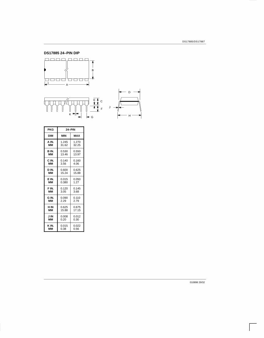
DS17885 24–PIN DIP
A
B
CE
F
G H
J
K
D
1
PKG 24–PIN
DIM MIN MAX
A IN.MM
1.24531.62
1.27032.25
B IN.MM
0.53013.46
0.55013.97
C IN.MM
0.1403.56
0.1604.06
D IN.MM
0.60015.24
0.62515.88
E IN.MM
0.0150.380
0.0501.27
F IN.MM
0.1203.05
0.1453.68
G IN.MM
0.0902.29
0.1102.79
H INMM
0.62515.88
0.67517.15
J INMM
0.0080.20
0.0120.30
K IN.MM
0.0150.38
0.0220.56

DS17885/DS17887
010898 30/32
DS17885 24–PIN SOIC
The chamfer on the body is optional. If it is not present, aterminal 1 identifier must be positioned so that 1/2 ormore of its area is contained in the hatched zone.
PKG 24–PIN
DIM MIN MAX
A IN.MM
0.0942.38
0.1052.68
A1 IN.MM
0.0040.102
0.0120.30
A2 IN.MM
0.0892.26
0.0952.41
b IN.MM
0.0130.33
0.0200.51
C INMM
0.0090.229
0.0130.33
D IN.MM
0.59815.19
0.61215.54
e IN.MM
0.050 BSC1.27 BSC
E1 IN.MM
0.2907.37
0.3007.62
H INMM
0.39810.11
0.41610.57
L INMM
0.0160.40
0.0401.02
Θ 0° 8°

DS17885/DS17887
010898 31/32
DS17885 28–PIN TSOP
PKG 28–PIN
DIM MIN MAX
A – 1.20
A1 0.05 –
A2 0.91 1.02
b 0.18 0.27
c 0.15 0.20
D 13.20 13.60
D1 11.70 11.90
E 7.90 8.10
e 0.55 BSC
L 0.30 0.70
L1 0.80 BSC
56–G5003–000

DS17885/DS17887
010898 32/32
DS17887 REAL TIME CLOCK PLUS RAM
A
24
1 12
13
C E
F
KD
11 EQUAL SPACES AT.100 .010 TNA±
G
B
H
J
NOTE: PINS 2, 3, 16, AND 20 ARE MISSING BYDESIGN.DIM MIN MAX
24–PINPKG
A IN.MM
B IN.MM
C IN.MM
D IN.MM
E IN.MM
F IN.MM
G IN.MM
H IN.MM
J IN.MM
K IN.MM
1.32033.53
1.33533.91
0.72018.29
0.74018.80
0.3458.76
0.3709.40
0.1002.54
0.1303.30
0.0150.38
0.0300.76
0.1102.79
0.1403.56
0.0902.29
0.1102.79
0.59014.99
0.63016.00
0.0080.20
0.0120.30
0.0150.38
0.0210.53