drj (qfn) package - farnell element14 · drj (qfn) package (topview) i nc q d pwm st gnd ref ......
TRANSCRIPT
1FEATURES
1
2
3
4
8
7
6
5
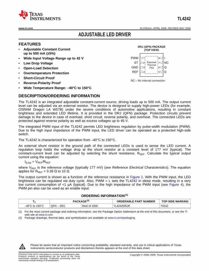
DRJ (QFN) PACKAGE
(TOP VIEW)
I
NC
Q
D
PWM
ST
GND
REF
NC – No internal connection
ExposedThermal
Pad
DESCRIPTION/ORDERING INFORMATION
TL4242
www.ti.com .............................................................................................................................................................. SLVS641A–APRIL 2008–REVISED MAY 2009
ADJUSTABLE LED DRIVER
• Adjustable Constant Currentup to 500 mA (±5%)
• Wide Input Voltage Range up to 42 V• Low Drop Voltage• Open-Load Detection• Overtemperature Protection• Short-Circuit Proof• Reverse-Polarity Proof• Wide Temperature Range: –40°C to 150°C
The TL4242 is an integrated adjustable constant-current source, driving loads up to 500 mA. The output currentlevel can be adjusted via an external resistor. The device is designed to supply high-power LEDs (for example,OSRAM Dragon LA W57B) under the severe conditions of automotive applications, resulting in constantbrightness and extended LED lifetime. It is provided in the DRJ (QFN) package. Protection circuits preventdamage to the device in case of overload, short circuit, reverse polarity, and overheat. The connected LEDs areprotected against reverse polarity as well as excess voltages up to 45 V.
The integrated PWM input of the TL4242 permits LED brightness regulation by pulse-width modulation (PWM).Due to the high input impedance of the PWM input, the LED driver can be operated as a protected high-sideswitch.
The TL4242 is characterized for operation from –40°C to 150°C.
An external shunt resistor in the ground path of the connected LEDs is used to sense the LED current. Aregulation loop holds the voltage drop at the shunt resistor at a constant level of 177 mV (typical). Theconstant-current level can be adjusted by selecting the shunt resistance, RREF. Calculate the typical outputcurrent using the equation:
IQ,typ = VREF/RREF
where VREF is the reference voltage (typically 177 mV) (see Reference Electrical Characteristics). The equationapplies for RREF = 0.39 Ω to 10 Ω.
The output current is shown as a function of the reference resistance in Figure 1. With the PWM input, the LEDbrightness can be regulated via duty cycle. Also, PWM = L sets the TL4242 in sleep mode, resulting in a verylow current consumption of <1 µA (typical). Due to the high impedance of the PWM input (see Figure 4), thePWM pin also can be used as an enable input.
ORDERING INFORMATION (1)
TJ PACKAGE (2) ORDERABLE PART NUMBER TOP-SIDE MARKING–40°C to 150°C QFN – DRJ Reel of 1000 TL4242DRJR T4242
(1) For the most current package and ordering information, see the Package Option Addendum at the end of this document, or see the TIweb site at www.ti.com.
(2) Package drawings, thermal data, and symbolization are available at www.ti.com/packaging.
1
Please be aware that an important notice concerning availability, standard warranty, and use in critical applications of TexasInstruments semiconductor products and disclaimers thereto appears at the end of this data sheet.
PRODUCTION DATA information is current as of publication date. Copyright © 2008–2009, Texas Instruments IncorporatedProducts conform to specifications per the terms of the TexasInstruments standard warranty. Production processing does notnecessarily include testing of all parameters.

QI
GND
PWM
ST
REF
D
Bias Supply
BandgapReference
Comparator
+
−
StatusDelay
8
4
5
6
3
2
1
TL4242
SLVS641A–APRIL 2008–REVISED MAY 2009 .............................................................................................................................................................. www.ti.com
TERMINAL FUNCTIONSNO. NAME DESCRIPTION
1 PWM Pulse-width modulation input. If not used, connect to I.2 ST Status output. Open-collector output. Connect to an external pullup resistor (RPULLUP ≥ 4.7 kΩ).3 GND Ground4 REF Reference input. Connect to a shunt resistor.5 D Status delay. To set status reaction delay, connect to GND with a capacitor. If no delay is needed, leave open.6 Q Output7 NC No internal connection8 I Input. Connect directly to GND as close as possible to the device with a 100-nF ceramic capacitor.
Thermal The thermal pad must be soldered directly to the PCB. It may be connected to ground or left floating.Pad
FUNCTIONAL BLOCK DIAGRAM
2 Submit Documentation Feedback Copyright © 2008–2009, Texas Instruments Incorporated
ABSOLUTE MAXIMUM RATINGS (1)
RECOMMENDED OPERATING CONDITIONS
OVERALL DEVICE ELECTRICAL CHARACTERISTICS
TL4242
www.ti.com .............................................................................................................................................................. SLVS641A–APRIL 2008–REVISED MAY 2009
over operating free-air temperature range (unless otherwise noted)
MIN MAX UNITVCC Supply voltage range (2) –42 45 V
D –0.3 7 VVI Input voltage range PWM –40 40 V
REF –1 16 VQ –1 41 V
VO Output voltage rangeST –0.3 40 VPWM ±1 mA
IO Output current range REF ±2 mAST ±5 mAJESD 51-5 (4) 49.5
θJA Thermal impedance, junction to ambient (3) °C/WJESD 51-7 (5) 114.4
θJP Thermal impedance, junction to pad (3) 4.4 °C/WTJ Virtual-junction temperature range –40 150 °CTstg Storage temperature range –50 150 °C
(1) Stresses beyond those listed under Absolute Maximum Ratings may cause permanent damage to the device. These are stress ratingsonly, and functional operation of the device at these or any other conditions beyond those indicated under Recommended OperatingConditions is not implied. Exposure to absolute-maximum-rated conditions for extended periods may affect device reliability.
(2) All voltage values are with respect to the network ground terminal.(3) Maximum power dissipation is a function of TJ(max), θJA, and TA. The maximum allowable power dissipation at any allowable ambient
temperature is PD = (TJ(max) – TA)/θJA. Operating at the absolute maximum TJ of 150°C can affect reliability.(4) The package thermal impedance is calculated in accordance with JESD 51-5.(5) The package thermal impedance is calculated in accordance with JESD 51-7.
MIN MAX UNITVCC Supply voltage 4.5 42 VVST Status (ST) output voltage 16 VVPWM PWM voltage 0 40 VCD Status delay (D) capacitance 0 2.2 µFRREF Reference (REF) resistor 0 10 ΩTJ Virtual-junction temperature –40 150 °C
over recommended operating free-air temperature range, VI = 13.5 V, RREF = 0.47 Ω, VPWM,H, TJ = –40°C to 150°C, allvoltages with respect to ground (unless otherwise noted)
PARAMETER TEST CONDITIONS MIN TYP MAX UNITIqL Supply current VQ = 6.6 V 12 22 mAIqOFF Supply current, off mode PWM = L, TJ < 85°C 0.1 2 µA
Copyright © 2008–2009, Texas Instruments Incorporated Submit Documentation Feedback 3

OUTPUT ELECTRICAL CHARACTERISTICS
PWM INPUT ELECTRICAL CHARACTERISTICS
REFERENCE (REF) ELECTRICAL CHARACTERISTICS
STATUS OUTPUT (ST) ELECTRICAL CHARACTERISTICS
STATUS DELAY (D) ELECTRICAL CHARACTERISTICS
TL4242
SLVS641A–APRIL 2008–REVISED MAY 2009 .............................................................................................................................................................. www.ti.com
over recommended operating free-air temperature range, VI = 13.5 V, RREF = 0.47 Ω, VPWM,H, TJ = –40°C to 150°C, allvoltages with respect to ground (unless otherwise noted)
PARAMETER TEST CONDITIONS MIN TYP MAX UNITVQ – VREF
(1) = 6.6 V 357 376 395VQ – VREF = 6.6 V, RREF = 1 Ω 168 177 185
IQ Output current mAVQ – VREF = 6.6 V, RREF = 0.39 Ω 431 454 476VQ – VREF = 5.4 V to 7.8 V, VI = 9 V to 16 V 357 376 395
IQmax Output current limit RREF = 0 Ω 600 mAVdr Drop voltage IQ = 300 mA 0.35 0.7 V
(1) VQ – VREF equals the forward voltage sum of the connected LEDs (see Figure 3).
over recommended operating free-air temperature range, VI = 13.5 V, RREF = 0.47 Ω, VPWM,H, TJ = –40°C to 150°C, allvoltages with respect to ground (unless otherwise noted)
PARAMETER TEST CONDITIONS MIN TYP MAX UNITVPWM, High-level PWM voltage 2.6 VH
VPWM, Low-level PWM voltage 0.7 VL
IPWM,H High-level PWM input current VPWM = 5 V 220 500 µAIPWM,L Low-level PWM input current VPWM = 0 V –1 1 µAtPWM,O Delay time, turn on 70% of IQnom, See Figure 6 0 15 40 µsN
tPWM,O Delay time, turn off 30% of IQnom, See Figure 6 0 15 40 µsFF
over recommended operating free-air temperature range, VI = 13.5 V, RREF = 0.47 Ω, VPWM,H, TJ = –40°C to 150°C, allvoltages with respect to ground (unless otherwise noted)
PARAMETER TEST CONDITIONS MIN TYP MAX UNITVREF Reference voltage RREF = 0.39 Ω to 1 Ω 168 177 185 mVIREF Reference input current VREF = 180 mV –1 0.1 1 µA
over recommended operating free-air temperature range, VI = 13.5 V, RREF = 0.47 Ω, VPWM,H, TJ = –40°C to 150°C, allvoltages with respect to ground (unless otherwise noted)
PARAMETER TEST CONDITIONS MIN TYP MAX UNITVIQL Lower status-switching threshold ST = L 15 25 mVVIQH Upper status-switching threshold ST = H 30 40 mVVSTL Low-level status voltage IST = 1.5 mA 0.4 VISTLK Leakage current VST = 5 V 5 µA
over recommended operating free-air temperature range, VI = 13.5 V, RREF = 0.47 Ω, VPWM,H, TJ = –40°C to 150°C, allvoltages with respect to ground (unless otherwise noted)
PARAMETER TEST CONDITIONS MIN TYP MAX UNITtSTHL Delay time, status reaction CD = 47 nF, ST H→L 6 10 14 mstSTLH Delay time, status release CD = 47 nF, ST L→H 10 20 µs
4 Submit Documentation Feedback Copyright © 2008–2009, Texas Instruments Incorporated
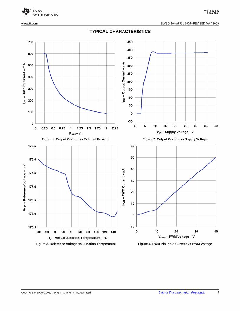
TYPICAL CHARACTERISTICS
-50
0
50
100
150
200
250
300
350
400
450
0 5 10 15 20 25 30 35 40
VCC – Supply Voltage – V
I OU
T–
Ou
tpu
tC
urr
en
t–
mA
0
100
200
300
400
500
600
700
0 0.25 0.5 0.75 1 1.25 1.5 1.75 2 2.25
RREF – 8
I OU
T–
Ou
tpu
tC
urr
en
t–
mA
W
-10
0
10
20
30
40
50
60
0 10 20 30 40
VPWM – PWM Voltage – V
I PW
M–
PW
MC
urr
en
t–
µA
175.5
176.0
176.5
177.0
177.5
178.0
178.5
-40 -20 0 20 40 60 80 100 120 140
TJ – Virtual Junction Temperature – °C
VR
EF
–R
efe
ren
ce
Vo
ltag
e–
mV
TL4242
www.ti.com .............................................................................................................................................................. SLVS641A–APRIL 2008–REVISED MAY 2009
Figure 1. Output Current vs External Resistor Figure 2. Output Current vs Supply Voltage
Figure 3. Reference Voltage vs Junction Temperature Figure 4. PWM Pin Input Current vs PWM Voltage
Copyright © 2008–2009, Texas Instruments Incorporated Submit Documentation Feedback 5
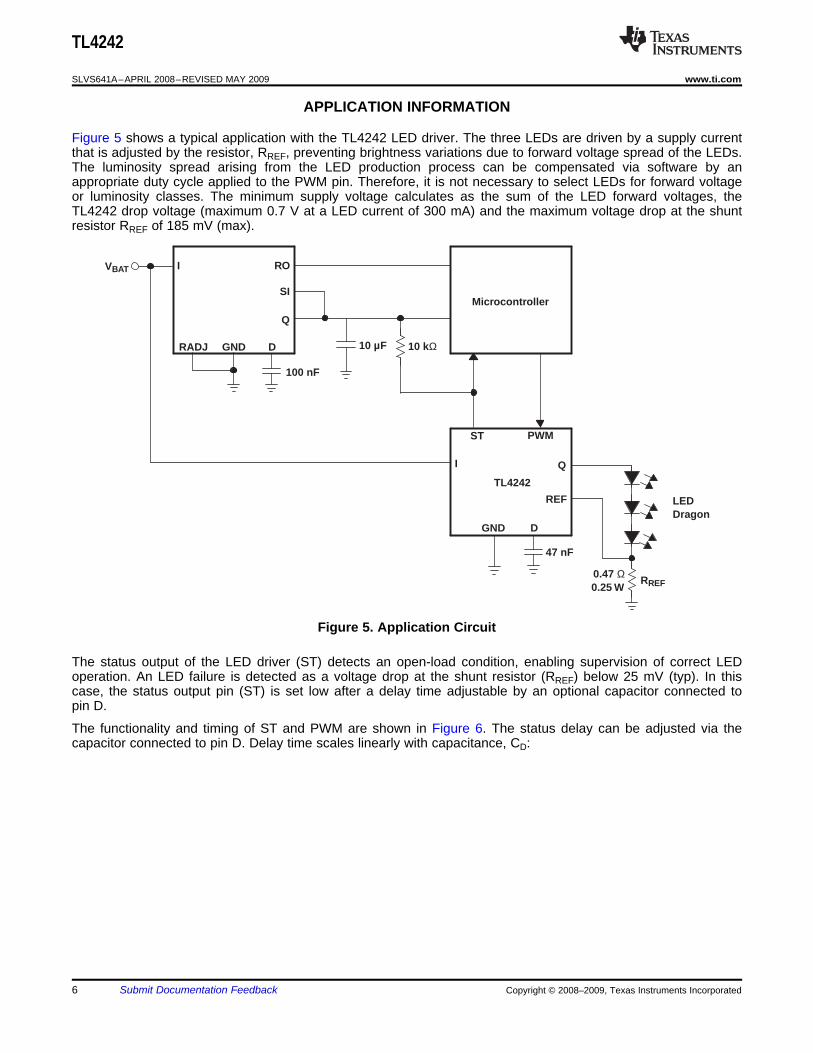
APPLICATION INFORMATION
100 nF
Q
SI
ROI
GNDRADJ D 10 µF 10 kΩ
ST PWM
GND D
47 nF
Q
REF
VBAT
RREF
LEDDragon
I
Microcontroller
0.47 Ω0.25 W
TL4242
TL4242
SLVS641A–APRIL 2008–REVISED MAY 2009 .............................................................................................................................................................. www.ti.com
Figure 5 shows a typical application with the TL4242 LED driver. The three LEDs are driven by a supply currentthat is adjusted by the resistor, RREF, preventing brightness variations due to forward voltage spread of the LEDs.The luminosity spread arising from the LED production process can be compensated via software by anappropriate duty cycle applied to the PWM pin. Therefore, it is not necessary to select LEDs for forward voltageor luminosity classes. The minimum supply voltage calculates as the sum of the LED forward voltages, theTL4242 drop voltage (maximum 0.7 V at a LED current of 300 mA) and the maximum voltage drop at the shuntresistor RREF of 185 mV (max).
Figure 5. Application Circuit
The status output of the LED driver (ST) detects an open-load condition, enabling supervision of correct LEDoperation. An LED failure is detected as a voltage drop at the shunt resistor (RREF) below 25 mV (typ). In thiscase, the status output pin (ST) is set low after a delay time adjustable by an optional capacitor connected topin D.
The functionality and timing of ST and PWM are shown in Figure 6. The status delay can be adjusted via thecapacitor connected to pin D. Delay time scales linearly with capacitance, CD:
6 Submit Documentation Feedback Copyright © 2008–2009, Texas Instruments Incorporated

tSTHL,typCD
47 nF 10 ms
tSTLH,typCD
47 nF 10 s
tPWM,OFF
30%
70%
tPWM,ON
tSTHL
Open
Load
Open
Load
t
t
t
t
VPWM
VPWM,H
VPWM,L
IQ,nom
IQ
VLD
VD
VST
TL4242
www.ti.com .............................................................................................................................................................. SLVS641A–APRIL 2008–REVISED MAY 2009
Figure 6. Function and Timing Diagram
Copyright © 2008–2009, Texas Instruments Incorporated Submit Documentation Feedback 7
PACKAGE OPTION ADDENDUM
www.ti.com 7-Jun-2013
Addendum-Page 1
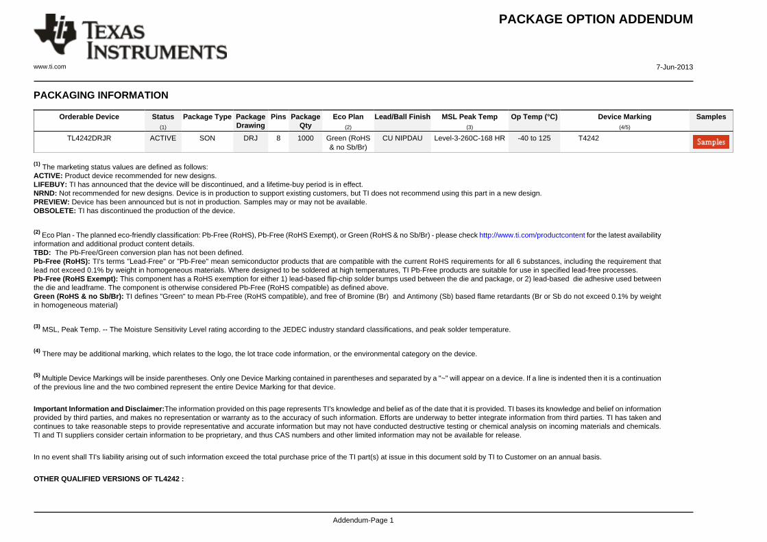
PACKAGING INFORMATION
Orderable Device Status(1)
Package Type PackageDrawing
Pins PackageQty
Eco Plan(2)
Lead/Ball Finish MSL Peak Temp(3)
Op Temp (°C) Device Marking(4/5)
Samples
TL4242DRJR ACTIVE SON DRJ 8 1000 Green (RoHS& no Sb/Br)
CU NIPDAU Level-3-260C-168 HR -40 to 125 T4242
(1) The marketing status values are defined as follows:ACTIVE: Product device recommended for new designs.LIFEBUY: TI has announced that the device will be discontinued, and a lifetime-buy period is in effect.NRND: Not recommended for new designs. Device is in production to support existing customers, but TI does not recommend using this part in a new design.PREVIEW: Device has been announced but is not in production. Samples may or may not be available.OBSOLETE: TI has discontinued the production of the device.
(2) Eco Plan - The planned eco-friendly classification: Pb-Free (RoHS), Pb-Free (RoHS Exempt), or Green (RoHS & no Sb/Br) - please check http://www.ti.com/productcontent for the latest availabilityinformation and additional product content details.TBD: The Pb-Free/Green conversion plan has not been defined.Pb-Free (RoHS): TI's terms "Lead-Free" or "Pb-Free" mean semiconductor products that are compatible with the current RoHS requirements for all 6 substances, including the requirement thatlead not exceed 0.1% by weight in homogeneous materials. Where designed to be soldered at high temperatures, TI Pb-Free products are suitable for use in specified lead-free processes.Pb-Free (RoHS Exempt): This component has a RoHS exemption for either 1) lead-based flip-chip solder bumps used between the die and package, or 2) lead-based die adhesive used betweenthe die and leadframe. The component is otherwise considered Pb-Free (RoHS compatible) as defined above.Green (RoHS & no Sb/Br): TI defines "Green" to mean Pb-Free (RoHS compatible), and free of Bromine (Br) and Antimony (Sb) based flame retardants (Br or Sb do not exceed 0.1% by weightin homogeneous material)
(3) MSL, Peak Temp. -- The Moisture Sensitivity Level rating according to the JEDEC industry standard classifications, and peak solder temperature.
(4) There may be additional marking, which relates to the logo, the lot trace code information, or the environmental category on the device.
(5) Multiple Device Markings will be inside parentheses. Only one Device Marking contained in parentheses and separated by a "~" will appear on a device. If a line is indented then it is a continuationof the previous line and the two combined represent the entire Device Marking for that device.
Important Information and Disclaimer:The information provided on this page represents TI's knowledge and belief as of the date that it is provided. TI bases its knowledge and belief on informationprovided by third parties, and makes no representation or warranty as to the accuracy of such information. Efforts are underway to better integrate information from third parties. TI has taken andcontinues to take reasonable steps to provide representative and accurate information but may not have conducted destructive testing or chemical analysis on incoming materials and chemicals.TI and TI suppliers consider certain information to be proprietary, and thus CAS numbers and other limited information may not be available for release.
In no event shall TI's liability arising out of such information exceed the total purchase price of the TI part(s) at issue in this document sold by TI to Customer on an annual basis.
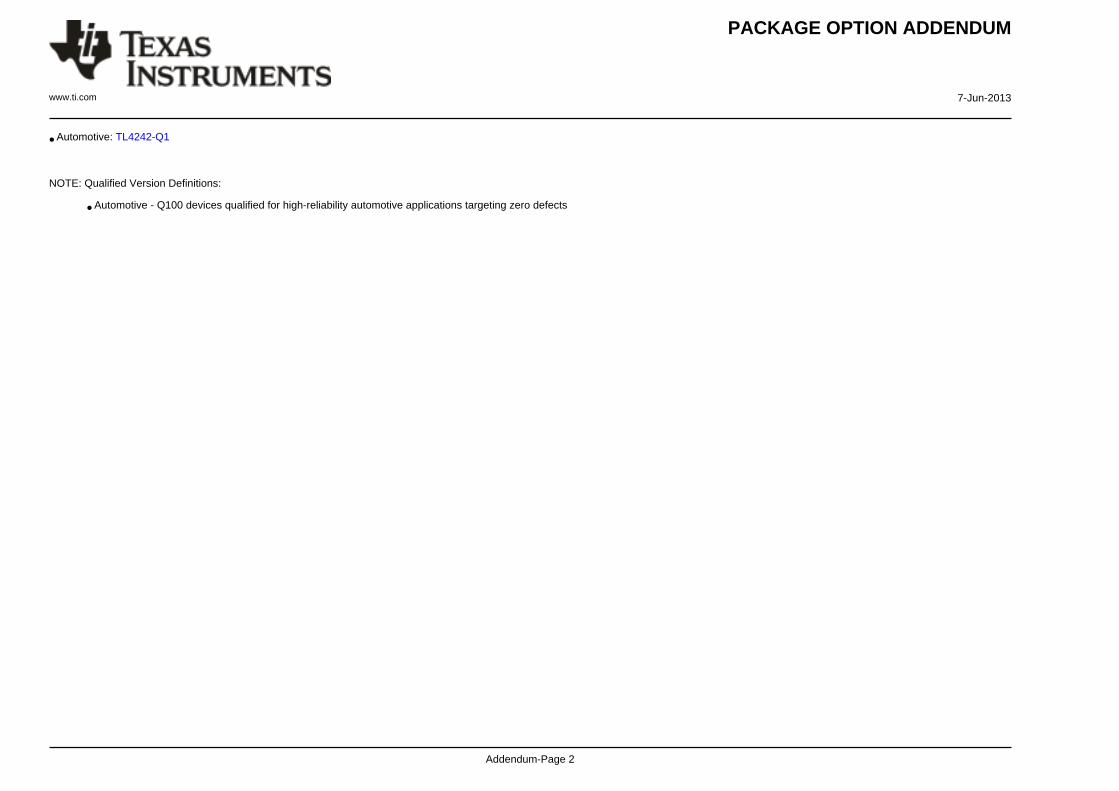
OTHER QUALIFIED VERSIONS OF TL4242 :
PACKAGE OPTION ADDENDUM
www.ti.com 7-Jun-2013
Addendum-Page 2
• Automotive: TL4242-Q1
NOTE: Qualified Version Definitions:
• Automotive - Q100 devices qualified for high-reliability automotive applications targeting zero defects

TAPE AND REEL INFORMATION
*All dimensions are nominal
Device PackageType
PackageDrawing
Pins SPQ ReelDiameter
(mm)
ReelWidth
W1 (mm)
A0(mm)
B0(mm)
K0(mm)
P1(mm)
W(mm)
Pin1Quadrant
TL4242DRJR SON DRJ 8 1000 180.0 12.4 4.25 4.25 1.15 8.0 12.0 Q2
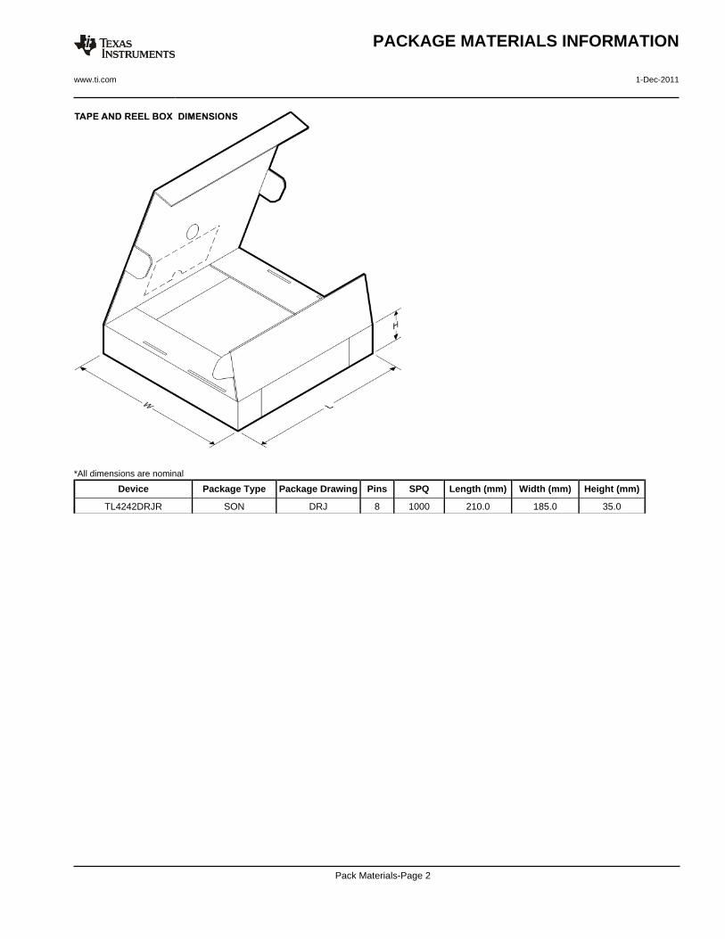
PACKAGE MATERIALS INFORMATION
www.ti.com 1-Dec-2011
Pack Materials-Page 1
*All dimensions are nominal
Device Package Type Package Drawing Pins SPQ Length (mm) Width (mm) Height (mm)
TL4242DRJR SON DRJ 8 1000 210.0 185.0 35.0
PACKAGE MATERIALS INFORMATION
www.ti.com 1-Dec-2011
Pack Materials-Page 2


IMPORTANT NOTICE
Texas Instruments Incorporated and its subsidiaries (TI) reserve the right to make corrections, enhancements, improvements and otherchanges to its semiconductor products and services per JESD46, latest issue, and to discontinue any product or service per JESD48, latestissue. Buyers should obtain the latest relevant information before placing orders and should verify that such information is current andcomplete. All semiconductor products (also referred to herein as “components”) are sold subject to TI’s terms and conditions of salesupplied at the time of order acknowledgment.
TI warrants performance of its components to the specifications applicable at the time of sale, in accordance with the warranty in TI’s termsand conditions of sale of semiconductor products. Testing and other quality control techniques are used to the extent TI deems necessaryto support this warranty. Except where mandated by applicable law, testing of all parameters of each component is not necessarilyperformed.
TI assumes no liability for applications assistance or the design of Buyers’ products. Buyers are responsible for their products andapplications using TI components. To minimize the risks associated with Buyers’ products and applications, Buyers should provideadequate design and operating safeguards.
TI does not warrant or represent that any license, either express or implied, is granted under any patent right, copyright, mask work right, orother intellectual property right relating to any combination, machine, or process in which TI components or services are used. Informationpublished by TI regarding third-party products or services does not constitute a license to use such products or services or a warranty orendorsement thereof. Use of such information may require a license from a third party under the patents or other intellectual property of thethird party, or a license from TI under the patents or other intellectual property of TI.
Reproduction of significant portions of TI information in TI data books or data sheets is permissible only if reproduction is without alterationand is accompanied by all associated warranties, conditions, limitations, and notices. TI is not responsible or liable for such altereddocumentation. Information of third parties may be subject to additional restrictions.
Resale of TI components or services with statements different from or beyond the parameters stated by TI for that component or servicevoids all express and any implied warranties for the associated TI component or service and is an unfair and deceptive business practice.TI is not responsible or liable for any such statements.
Buyer acknowledges and agrees that it is solely responsible for compliance with all legal, regulatory and safety-related requirementsconcerning its products, and any use of TI components in its applications, notwithstanding any applications-related information or supportthat may be provided by TI. Buyer represents and agrees that it has all the necessary expertise to create and implement safeguards whichanticipate dangerous consequences of failures, monitor failures and their consequences, lessen the likelihood of failures that might causeharm and take appropriate remedial actions. Buyer will fully indemnify TI and its representatives against any damages arising out of the useof any TI components in safety-critical applications.
In some cases, TI components may be promoted specifically to facilitate safety-related applications. With such components, TI’s goal is tohelp enable customers to design and create their own end-product solutions that meet applicable functional safety standards andrequirements. Nonetheless, such components are subject to these terms.
No TI components are authorized for use in FDA Class III (or similar life-critical medical equipment) unless authorized officers of the partieshave executed a special agreement specifically governing such use.
Only those TI components which TI has specifically designated as military grade or “enhanced plastic” are designed and intended for use inmilitary/aerospace applications or environments. Buyer acknowledges and agrees that any military or aerospace use of TI componentswhich have not been so designated is solely at the Buyer's risk, and that Buyer is solely responsible for compliance with all legal andregulatory requirements in connection with such use.
TI has specifically designated certain components as meeting ISO/TS16949 requirements, mainly for automotive use. In any case of use ofnon-designated products, TI will not be responsible for any failure to meet ISO/TS16949.
Products Applications
Audio www.ti.com/audio Automotive and Transportation www.ti.com/automotive
Amplifiers amplifier.ti.com Communications and Telecom www.ti.com/communications
Data Converters dataconverter.ti.com Computers and Peripherals www.ti.com/computers
DLP® Products www.dlp.com Consumer Electronics www.ti.com/consumer-apps
DSP dsp.ti.com Energy and Lighting www.ti.com/energy
Clocks and Timers www.ti.com/clocks Industrial www.ti.com/industrial
Interface interface.ti.com Medical www.ti.com/medical
Logic logic.ti.com Security www.ti.com/security
Power Mgmt power.ti.com Space, Avionics and Defense www.ti.com/space-avionics-defense
Microcontrollers microcontroller.ti.com Video and Imaging www.ti.com/video
RFID www.ti-rfid.com
OMAP Applications Processors www.ti.com/omap TI E2E Community e2e.ti.com
Wireless Connectivity www.ti.com/wirelessconnectivity
Mailing Address: Texas Instruments, Post Office Box 655303, Dallas, Texas 75265Copyright © 2013, Texas Instruments Incorporated