Digital System Design
D e p t . o f E C E , S I E T K Page 1
UUUUNNNNIIIITTTT IIII
CCCCMMMMOOOOSSSS LLLLOOOOGGGGIIIICCCC
Introduction to Logic Families:
There are many, many ways to design an electronic logic circuit.
1. The first electrically controlled logic circuits, developed at Bell Laboratories in 1930s,
were based on relays.
2. In the mid-1940s, the first electronic digital computer, the Eniac, used logic circuits
based on vacuum tubes. The Eniac had about 18,000 tubes and a similar number of logic
gates, not a lot by today’s standards of microprocessor chips with tens of millions of
transistors. However, the Eniac could hurt you a lot more than a chip could if it fell on
you—it was 100 feet long, 10 feet high, 3 feet deep, and consumed 140,000 watts of
power!
3. The inventions of the semiconductor diode and the bipolar junction transistor allowed
the development of smaller, faster, and more capable computers in the late 1950s.
4. In the 1960s, the invention of the integrated circuit (IC) allowed multiple diodes,
transistors, and other components to be fabricated on a single chip, and computers got
still better.

Digital System Design
D e p t . o f E C E , S I E T K Page 2
A llllooooggggiiiicccc ffffaaaammmmiiiillllyyyy:::: is a collection of different integrated-circuit chips that have similar input,
output, and internal circuit characteristics, but that perform different logic functions. Chips
from the same family can be interconnected to perform any desired logic function.
CMOS Logic::::
The functional behavior of a CMOS logic circuit is fairly easy to understand, even if
your knowledge of analog electronics is not particularly deep. The basic (and typically
only) building blocks in CMOS logic circuits are MOS transistors, described shortly. Before
introducing MOS transistors and CMOS logic circuits, we must talk about logic levels.
CMOS Logic Levels:
Abstract logic elements process binary digits, 0 and 1. However, real logic circuits
process electrical signals such as voltage levels. In any logic circuit, there is a range of
voltages (or other circuit conditions) that is interpreted as a logic 0, and another, non
overlapping range that is interpreted as a logic 1. A typical CMOS logic circuit operates
from a 5-volt power supply. Such a circuit may interpret any voltage in the range 0–1.5 V
as a logic 0, and in the range 3.5–5.0 V as a logic 1. Thus, the definitions of LOW and
HIGH for 5-volt CMOS logic are as shown in Figure. Voltages in the intermediate range
are not expected to occur except during signal transitions, and yield undefined logic values
(i.e., a circuit may interpret them as either 0 or 1). CMOS circuits using other power supply
voltages, such as 3.3 or 2.7 volts, partition the voltage range similarly.

Digital System Design
D e p t . o f E C E , S I E T K Page 3
MOS Transistors:
A MOS transistor can be modeled as a 3-terminal device that acts like a voltage
controlled resistance. As suggested by Figure, an input voltage applied to one terminal
controls the resistance between the remaining two terminals. In digital logic applications, a
MOS transistor is operated so its resistance is always either very high (and the transistor is
“off”) or very low (and the transistor is “on”).
There are two types of MOS transistors, n-channel and p-channel; the names refer to the
type of semiconductor material used for the resistance-controlled terminals.
nnnn----cccchhhhaaaannnnnnnneeeellll MMMMOOOOSSSS ((((NNNNMMMMOOOOSSSS)))) ttttrrrraaaannnnssssiiiissssttttoooorrrr::::
The circuit symbol for an n-channel MOS (NMOS) transistor is shown in Figure .
The terminals are called gate, source, and drain. (Note that the “gate” of a MOS transistor

Digital System Design
D e p t . o f E C E , S I E T K Page 4
has nothing to do with a “logic gate.”) As you might guess from the orientation of the circuit
symbol, the drain is normally at a higher voltage than the source. The voltage from gate to
source (Vgs) in an NMOS transistor is normally zero or positive. If Vgs = 0, then the
resistance from drain to source (Rds) is very high, on the order of a megohm (106 ohms)
or more. As we increase Vgs (i.e., increase the voltage on the gate), Rds decreases to a
very low value, 10 ohms or less in some devices.
pppp----cccchhhhaaaannnnnnnneeeellll MMMMOOOOSSSS ((((PPPPMMMMOOOOSSSS)))) ttttrrrraaaannnnssssiiiissssttttoooorrrr:
The circuit symbol for a p-channel MOS (PMOS) transistor is shown in Figure.
Operation is analogous to that of an NMOS transistor, except that the source is normally
at a higher voltage than the drain, and Vgs is normally zero or negative. If Vgs is zero,
then the resistance from source to drain (Rds) is very high. As we algebraically decrease
Vgs (i.e., decrease the voltage on the gate), Rds decreases to a very low value.

Digital System Design
D e p t . o f E C E , S I E T K Page 5
The gate of a MOS transistor has very high impedance. That is, the gate is separated from
the source and the drain by an insulating material with a very high resistance. However,
the gate voltage creates an electric field that enhances or retards the flow of current
between source and drain. This is the “field effect” in the “MOSFET” name.
Basic CMOS Inverter Circuit:
NMOS and PMOS transistors are used together in a complementary way to form
CMOS logic. The simplest CMOS circuit, a logic inverter, requires only one of each type of
transistor, connected as shown in Figure. The power supply voltage, VDD, typically may
be in the range 2–6 V, and is most often set at 5.0 V for compatibility with TTL circuits.
Ideally, the functional behavior of the CMOS inverter circuit can be characterized by
just two cases tabulated in Figure:
1. VIN is 0.0 V. In this case, the bottom, n-channel transistor Q1 is off, since its Vgs is 0,
but the top, p-channel transistor Q2 is on, since its Vgs is a large negative value ( 5.0 V).
Therefore, Q2 presents only a small resistance between the power supply terminal (VDD,
5.0 V) and the output terminal (VOUT), and the output voltage is 5.0 V.
2. VIN is 5.0 V. Here, Q1 is on, since its Vgs is a large positive value (+5.0 V), but Q2 is
off, since its Vgs is 0. Thus, Q1 presents a small resistance between the output terminal
and ground, and the output voltage is 0 V.

Digital System Design
D e p t . o f E C E , S I E T K Page 6
With the foregoing functional behavior, the circuit clearly behaves as a logical inverter,
since a 0-volt input produces a 5-volt output, and vice versa another way to visualize
CMOS operation uses switches. As shown in Figure, the n-channel (bottom) transistor is
modeled by a normally-open switch, and the p-channel (top) transistor by a normally-
closed switch. Applying a HIGH voltage changes each switch to the opposite of its normal
state, as shown in (b).

Digital System Design
D e p t . o f E C E , S I E T K Page 7
The switch model gives rise to a way of drawing CMOS circuits that makes their logical
behavior more readily apparent. As shown in Figure , different symbols are used for the
pand n-channel transistors to reflect their logical behavior. The n-channel transistor (Q1) is
switched “on,” and current flows between source and drain, when a HIGH voltage is
applied to its gate; this seems natural enough. The p-channel transistor (Q2) has the
opposite behavior. It is “on” when a LOW voltage is applied; the inversion bubble on its
gate indicates this inverting behavior.
CMOS NAND and NOR Gates:
Both NAND and NOR gates can be constructed using CMOS. A k-input gate uses k
pchannel and k n-channel transistors. Figure shows a 2-input CMOS NAND gate. If either
input is LOW, the output Z has a low-impedance connection to VDD through the
corresponding “on” p-channel transistor, and the path to ground is blocked by the
corresponding “off” n-channel transistor. If both inputs are HIGH, the path to VDD is

Digital System Design
D e p t . o f E C E , S I E T K Page 8
blocked, and Z has a low-impedance connection to ground. Figure shows the switch
model for the NAND gate’s operation.
Figure shows a CMOS NOR gate. If inputs are LOW, the output Z has a low impedance
connection to VDD through the “on” p-channel transistors, and the path to ground is
blocked by the “off” n-channel transistors. If either input is HIGH, the path to VDD is
blocked, and Z has a low-impedance connection to ground.

Digital System Design
D e p t . o f E C E , S I E T K Page 9
Fan-In:
The number of inputs that a gate can have in a particular logic family is called the logic
family’s fan-in. As the number of inputs is increased, CMOS gate designers may
compensate by increasing the size of the series transistors to reduce their resistance and
the corresponding switching delay. However, at some point this becomes inefficient or
impractical. Gates with a large number of inputs can be made faster and smaller by
cascading gates with fewer inputs.
Noninverting Gates:
In CMOS, and in most other logic families, the simplest gates are inverters, and the next
simplest are NAND gates and NOR gates. A logical inversion comes “for free,” and it
typically is not possible to design a noninverting gate with a smaller number of transistors
than an inverting one. CMOS noninverting buffers and AND and OR gates are obtained by
connecting an inverter to the output of the corresponding inverting gate.
CMOS AND-OR-INVERT and OR-AND-INVERT Gates:
CMOS circuits can perform two levels of logic with just a single “level” of transistors. For
example, the circuit in Figure is a two-wide, two-input CMOS AND-OR-INVERT (AOI)
gate. The function table for this circuit is shown in (b) and a logic diagram for this function
using AND and NOR gates is shown in Figure. Transistors can be added to or removed
from this circuit to obtain an AOI function with a different number of ANDs or a different
number of inputs per AND. The contents of each of the Q1–Q8 columns in Figure 0(b)
Digital System Design
D e p t . o f E C E , S I E T K Page 10
depends only on the input signal connected to the corresponding transistor’s gate. The
last column is constructed by examining each input combination and determining whether
Z is connected to VDD or ground by “on” transistors for that input combination. Note that Z
is never connected to both VDD and ground for any input combination; in such a case the
output would be a non-logic value some where between LOW and HIGH, and the output
structure would consume excessive power due to the low-impedance connection between
VDD and ground.

Digital System Design
D e p t . o f E C E , S I E T K Page 11
A circuit can also be designed to perform an OR-AND-INVERT function. For example,
Figure is a two-wide, two-input CMOS OR-AND-INVERT (OAI ) gate. The function table
for this circuit is shown in (b); the values in each column are determined just as we did for
the CMOS AOI gate.
Electrical Behavior of CMOS Circuits:
Electrical Behavior of CMOS Circuits:
• Logic voltage levels. CMOS devices operating under normal conditions are guaranteed
to produce output voltage levels within well-defined LOW and HIGH ranges. And they
recognize LOW and HIGH input voltage levels over somewhat wider ranges. CMOS
manufacturers specify these ranges and operating conditions very carefully to ensure

Digital System Design
D e p t . o f E C E , S I E T K Page 12
compatibility among different devices in the same family, and to provide a degree of
interoperability (if you’re careful) among devices in different families.
• DC noise margins. Nonnegative DC noise margins ensure that the highest LOW voltage
produced by an output is always lower than the highest voltage that an input can reliably
interpret as LOW, and that the lowest HIGH voltage produced by an output is always
higher than the lowest voltage that an input can reliably interpret as HIGH. A good
understanding of noise margins is especially important in circuits that use devices from a
number of different families.
• Fanout. This refers to the number and type of inputs that are connected to a given
output. If too many inputs are connected to an output, the DC noise margins of the circuit
may be inadequate. Fanout may also affect the speed at which the output changes from
one state to another.
• Speed. The time that it takes a CMOS output to change from the LOW state to the HIGH
state, or vice versa, depends on both the internal structure of the device and the
characteristics of the other devices that it drives, even to the extent of being affected by
the wire or printed circuit- board traces connected to the output. We’ll look at two separate
components of “speed”—transition time and propagation delay.
• Power consumption. The power consumed by a CMOS device depends on a number of
factors, including not only its internal structure, but also the input signals that it receives,

Digital System Design
D e p t . o f E C E , S I E T K Page 13
the other devices that it drives, and how often its output changes between LOW and
HIGH.
• Noise. The main reason for providing engineering design margins is to ensure proper
circuit operation in the presence of noise. Noise can be generated by a number of
sources; several of them are listed below, from the least likely to the (perhaps surprisingly)
most likely:
– Cosmic rays.
– Magnetic fields from nearby machinery.
– Power-supply disturbances.
– The switching action of the logic circuits themselves.
• Electrostatic discharge. Would you believe that you can destroy a CMOS device just by
touching it?
• Open-drain outputs. Some CMOS outputs omit the usual p-channel pull-up transistors. In
the HIGH state, such outputs are effectively a “no-connection,” which is useful in some
applications.
• Three-state outputs. Some CMOS devices have an extra “output enable” control input
that can be used to disable both the p-channel pull-up transistors and the n-channel pull-
down transistors. Many such device outputs can be tied together to create a multisource
bus, as long as the control logic is arranged so that at most one output is enabled at a
time.

Digital System Design
D e p t . o f E C E , S I E T K Page 14
CMOS Steady-State Electrical Behavior:
CMOS Steady-State Electrical Behavior:
Logic Levels and Noise Margins
VOHmin The minimum output voltage in the HIGH state.
VIHmin The minimum input voltage guaranteed to be recognized as a HIGH.
VILmax The maximum input voltage guaranteed to be recognized as a LOW.
VOLmax The maximum output voltage in the LOW state.
The input voltages are determined mainly by switching thresholds of the two transistors,
while the output voltages are determined mainly by the “on” resistance of the transistors.
The power-supply voltage VCC and ground are often called the power supply rails. CMOS
levels are typically a function of the power-supply rails:
VOHmin VCC 0.1 V
VIHmin 70% of VCC
VILmax 30% of VCC
VOLmax ground + 0.1 V
Digital System Design
D e p t . o f E C E , S I E T K Page 15
DDDDCCCC nnnnooooiiiisssseeee mmmmaaaarrrrggggiiiinnnn is a measure of how much noise it takes to corrupt a worst-case output
voltage into a value that may not be recognized properly by an input. For HC-series
CMOS in the LOW state, VILmax (1.35 V) exceeds VOLmax (0.1 V) by 1.25 V so the
LOW-state DC noise margin is 1.25 V. Likewise, there is DC noise margin of 1.25 V in the
HIGH state. In general, CMOS outputs have excellent DC noise margins when driving
other CMOS inputs. Regardless of the voltage applied to the input of a CMOS inverter, the
input consumes very little current, only the leakage current of the two transistors’ gates.
The maximum amount of current that can flow is also specified by the device
manufacturer:
IIH The maximum current that flows into the input in the LOW state.
IIL The maximum current that flows into the input in the HIGH state.
Circuit Behavior with Resistive Loads
As mentioned previously, CMOS gate inputs have very high impedance and consume very
little current from the circuits that drive them. There are other devices, however, which
require nontrivial amounts of current to operate. When such a device is connected to a
CMOS output, we call it a resistive load or a DC load. Here are some examples of
resistive loads:
• Discrete resistors may be included to provide transmission-line termination.
• Discrete resistors may not really be present in the circuit, but the load presented by one
or more TTL or other non-CMOS inputs may be modeled by a simple resistor network.

Digital System Design
D e p t . o f E C E , S I E T K Page 16
• The resistors may be part of or may model a current-consuming device such as a light-
emitting diode (LED) or a relay coil. When the output of a CMOS circuit is connected to a
resistive load, the output behavior is not nearly as ideal as we described previously. In
either logic state, the CMOS output transistor that is “on” has a nonzero resistance, and a
load connected to the output terminal will cause a voltage drop across this resistance.
Thus, in the LOW state, the output voltage may be somewhat higher than 0.1 V, and in the
HIGH state it may be lower than 4.4 V. The easiest way to see how this happens is look at a
resistive model of the CMOS circuit and load.
Circuit Behavior with Nonideal Inputs
So far, we have assumed that the HIGH and LOW inputs to a CMOS circuit are ideal
voltages, very close to the power-supply rails. However, the behavior of a real CMOS
inverter circuit depends on the input voltage as well as on the characteristics of the load. If
the input voltage is not close to the power-supply rail, then the “on” transistor may not be
fully “on” and its resistance may increase. Likewise, the “off” transistor may not be fully
“off’ and its resistance may be quite a bit less than one megohm. These two effects
combine to move the output voltage away from the power-supply rail.
Fanout
The fanout of a logic gate is the number of inputs that the gate can drive without
exceeding its worst-case loading specifications. The fanout depends not only on the
Digital System Design
D e p t . o f E C E , S I E T K Page 17
characteristics of the output, but also on the inputs that it is driving. Fanout must be
examined for both possible output states, HIGH and LOW.
Unused Inputs
Sometimes not all of the inputs of a logic gate are used. In a real design problem, you may
need an n-input gate but have only an n+1-input gate available. Tying together two inputs
of the n+1-input gate gives it the functionality of an n-input gate.
Current Spikes and Decoupling Capacitors
When a CMOS output switches between LOW and HIGH, current flows from VCC to
ground through the partially-on p- and n-channel transistors. These currents, often called
current spikes because of their brief duration, may show up as noise on the power-supply
and ground connections in a CMOS circuit, especially when multiple outputs are switched
simultaneously. For this reason, systems that use CMOS circuits require decoupling
capacitors between VCC and ground. These capacitors must be distributed throughout the
circuit, at least one within an inch or so of each chip, to supply current during transitions.
The large filtering capacitors typically found in the power supply itself don’t satisfy this
requirement, because stray wiring inductance prevents them from supplying the current
fast enough, hence the need for a physically distributed system of decoupling capacitors.
How to Destroy a CMOS Device
Hit it with a sledge hammer. Or simply walk across a carpet and then touch an input pin
with your finger. Because CMOS device inputs have such high impedance, they are
Digital System Design
D e p t . o f E C E , S I E T K Page 18
subject to damage from electrostatic discharge (ESD). ESD occurs when a buildup of
charge on one surface arcs through a dielectric to another surface with the opposite
charge. In the case of a CMOS input, the dielectric is the insulation between an input
transistor’s gate and its source and drain. ESD may damage this insulation, causing a
short-circuit between the device’s input and output. The input structures of modern CMOS
devices use various measures to reduce their susceptibility to ESD damage, but no device is
completely immune.
Therefore, to protect CMOS devices from ESD damage during shipment and
handling, manufacturers normally package their devices in conductive bags, tubes, or
foam. To prevent ESD damage when handling loose CMOS devices, circuit assemblers
and technicians usually wear conductive wrist straps that are connected by a coil cord to
earth ground; this prevents a static charge from building up on their bodies as they move
around the factory or lab. Once a CMOS device is installed in a system, another possible
source of damage is latch-up. The physical input structure of just about any CMOS device
contains parasitic bipolar transistors between VCC and ground configured as a silicon-
controlled rectifier (SCR).” In normal operation, this “parasitic SCR” has no effect on
device operation. However, an input voltage that is less than ground or more than VCC
can “trigger” the SCR, creating a virtual short-circuit between VCC and ground. Once the
SCR is triggered, the only way to turn it off is to turn off the power supply. Before you have
a chance to do this, enough power may be dissipated to destroy the device (i.e., you may

Digital System Design
D e p t . o f E C E , S I E T K Page 19
see smoke). One possible trigger for latch-up is “undershoot” on high-speed HIGH-to-
LOW signal transitions.
In this situation, the input signal may go several volts below ground for several
nanoseconds before settling into the normal LOW range. However, modern CMOS logic
circuits are fabricated with special structures that prevent latch-up in this transient case.
Latch-up can also occur when CMOS inputs are driven by the outputs of another system
or subsystem with a separate power supply. If a HIGH input is applied to a CMOS gate
before power is present, the gate may come up in the “latched-up” state when power is
applied. Again, modern CMOS logic circuits are fabricated with special structures that
prevent this in most cases. However, if the driving output is capable of sourcing lots of
current (e.g., tens of mA), latchup is still possible. One solution to this problem is to apply
power before hooking up input cables.
CMOS Dynamic Electrical Behavior:
CMOS Dynamic Electrical Behavior:
Both the speed and the power consumption of a CMOS device depend to a large
extent on AC or dynamic characteristics of the device and its load, that is, what happens
when the output changes between states. As part of the internal design of CMOS ASICs,
logic designers must carefully examine the effects of output loading and redesign where
the load is too high. Even in board-level design, the effects of loading must be considered
for clocks, buses, and other signals that have high fanout or long interconnections. Speed
depends on two characteristics, transition time and propagation delay.

Digital System Design
D e p t . o f E C E , S I E T K Page 20
Transition Time
The amount of time that the output of a logic circuit takes to change from one state to
another is called the transition time. Figure shows how we might like outputs to change
state—in zero time. However, real outputs cannot change instantaneously, because they
need time to charge the stray capacitance of the wires and other components that they
drive. A more realistic view of a circuit’s output is shown in (b). An output takes a certain
time, called the rise time (tr), to change from LOW to HIGH, and a possibly different time,
called the fall time (tf), to change from HIGH to LOW.
Even Figure (b) is not quite accurate, because the rate of change of the output voltage
does not change instantaneously, either. Instead, the beginning and the end of a transition
are smooth, as shown in (c). To avoid difficulties in defining the endpoints, rise and fall
times are normally measured at the boundaries of the valid logic levels as indicated in the
figure. With the convention in (c), the rise and fall times indicate how long an output
voltage takes to pass through the “undefined” region between LOW and HIGH. The initial

Digital System Design
D e p t . o f E C E , S I E T K Page 21
part of a transition is not included in the rise- or fall-time number. Instead, the initial part of
a transition contributes to the “propagation delay” number discussed in the next
subsection. The rise and fall times of a CMOS output depend mainly on two factors, the
“on” transistor resistance and the load capacitance. A large capacitance increases
transition times; since this is undesirable, it is very rare for a logic designer to purposely
connect a capacitor to a logic circuit’s output. However, stray capacitance is present in
every circuit; it comes from at least three sources:
1. Output circuits, including a gate’s output transistors, internal wiring, and packaging,
have some capacitance associated with them, on the order of picofarads (pF) in typical
logic families, including CMOS.
2. The wiring that connects an output to other inputs has capacitance, about 1 pF per inch
or more, depending on the wiring technology.
3. Input circuits, including transistors, internal wiring, and packaging, have capacitance,
from 2 to 15 pF per input in typical logic families.
Power Consumption
The power consumption of a CMOS circuit whose output is not changing is called static
power dissipation or quiescent power dissipation. (The words consumption and dissipation
are used pretty much interchangeably when discussing how much power a device uses.)
Most CMOS circuits have very low static power dissipation. This is what makes them so
attractive for laptop computers and other low-power applications—when computation

Digital System Design
D e p t . o f E C E , S I E T K Page 22
pauses, very little power is consumed. A CMOS circuit consumes significant power only
during transitions; this is called dynamic power dissipation.
One source of dynamic power dissipation is the partial short-circuiting of the CMOS
output structure. When the input voltage is not close to one of the power supply rails (0 V
or VCC), both the p-channel and n-channel output transistors may be partially “on,”
creating a series resistance of 600 � or less. In this case, current flows through the
transistors from VCC to ground. The amount of power consumed in this way depends on
both the value of VCC and the rate at which output transitions occur, according to the
formula The following variables are used in the formula:
PT The circuit’s internal power dissipation due to output transitions.
VCC The power supply voltage. As all electrical engineers know, power dissipation across a
resistive load (the partially-on transistors) is proportional to the square of the voltage.
f The transition frequency of the output signal. This specifies the number of power
consuming output transitions per second. (But note that frequency is defined as the
number of transitions divided by 2.)
CPD The power dissipation capacitance. This constant, normally specified by the device
manufacturer, completes the formula. CPD turns out to have units of capacitance, but
does not represent an actual output capacitance.

Digital System Design
D e p t . o f E C E , S I E T K Page 23
Three-State Outputs
Logic outputs have two normal states, LOW and HIGH, corresponding to logic values 0
and1. However, some outputs have a third electrical state that is not a logic state at all,
called the high impedance, Hi-Z, or floating state. In this state, the output behaves as if it
isn’t even connected to the circuit, except for a small leakage current that may flow into or
out of the output pin. Thus, an output can have one of three states—logic 0, logic 1, and
Hi-Z. An output with three possible states is called (surprise!) a three-state output or,
sometimes, a tri-state output. Three-state devices have an extra input, usually called
“output enable” or “output disable,” for placing the device’s output(s) in the high-
impedance state. A three-state bus is created by wiring several three-state outputs
together. Control circuitry for the “output enables” must ensure that at most one output is
enabled (not in its Hi-Z state) at any time. The single enabled device can transmit logic
levels (HIGH and LOW) on the bus.
Open-Drain Outputs
The p-channel transistors in CMOS output structures are said to provide active pull-up,
since they actively pull up the output voltage on a LOW-to-HIGH transition. These
transistors are omitted in gates with open-drain outputs,

Digital System Design
D e p t . o f E C E , S I E T K Page 24
CMOS Logic Families:
The first commercially successful CMOS family was 4000-series CMOS. Although
4000- series circuits offered the benefit of low power dissipation, they were fairly slow and
were not easy to interface with the most popular logic family of the time, bipolar TTL.
Thus, the 4000 series was supplanted in most applications by the more capable CMOS
families discussed in this section. All of the CMOS devices that we discuss have part
numbers of the form “74FAMnn,” where “FAM” is an alphabetic family mnemonic and nn is
a numeric function designator. Devices in different families with the same value of nn
perform the same function. For example, the 74HC30, 74HCT30, 74AC30, 74ACT30, and
74AHC30 are all 8-input NAND gates. The prefix “74” is simply a number that was used by
an early, popular supplier of TTL devices, Texas Instruments. The prefix “54” is used for
identical parts that are specified for operation over a wider range of temperature and
power-supply voltage, for use in military applications. Such parts are usually
Rmin = 5.0 – 0.0 IR(max) = 1562.5 �
IR(leak) = 4 � 5 + 2 � 20 = 60 �A
Rmax = 5.0 – 2.4 IR(leak) = 43.3 �
fabricated in the same way as their 74-series counterparts, except that they are tested,
screened, and marked differently, a lot of extra paperwork is generated, and a higher price
is charged, of course.

Digital System Design
D e p t . o f E C E , S I E T K Page 25
HC and HCT
The first two 74-series CMOS families are HC (High-speed CMOS) and HCT (High-
speed CMOS, TTL compatible). Compared with the original 4000 family, HC and HCT
both have higher speed and better current sinking and sourcing capability. The HCT family
uses a power supply voltage VCC of 5 V and can be intermixed with TTL devices, which
also use a 5-V supply. The HC family is optimized for use in systems that use CMOS logic
exclusively, and can use any power supply voltage between 2 and 6 V. A higher voltage is
used for higher speed, and a lower voltage for lower power dissipation. Lowering the
supply voltage is especially effective, since most CMOS power dissipation is proportional
to the square of the voltage (CV2f power). Even when used with a 5-V supply, HC devices
are not quite compatible with TTL.
VHC and VHCT
Several new CMOS families were introduced in the 1980s and the 1990s. Two of
the most recent and probably the most versatile are VHC (Very High-Speed CMOS) and
VHCT (Very High-Speed CMOS, TTL compatible). These families are about twice as fast
as HC HCT while maintaining backwards compatibility with their predecessors. Like HC
and HCT, the VHC and VHCT families differ from each other only in the input levels that
they recognize; their output characteristics are the same. Also like HC HCT, VHC VHCT
outputs have symmetric output drive. That is, an output can sink or source equal amounts
of current; the output is just as “strong” in both states. Other logic families, including the

Digital System Design
D e p t . o f E C E , S I E T K Page 26
FCT and TTL families introduced later, have asymmetric output drive; they can sink much
more current in the LOW state than they can source in the HIGH state.
HC, HCT, VHC, and VHCT Electrical Characteristics
Electrical characteristics of the HC, HCT, VHC, and VHCT families are summarized in
this subsection. The specifications assume that the devices are used with a nominal 5-V
power supply, although (derated) operation is possible with any supply voltage in the
range 2–5.5 V (up to 6 V for HC HCT). Commercial (74-series) parts are intended to be
operated at temperatures between 0�C and 70�C, while military (54-series) parts are
characterized for operation between 55�C and 125�C.
FCT and FCT-T
FCT and FCT-T
In the early 1990s, yet another CMOS family was launched. The key benefit of the
FCT (Fast CMOS, TTL compatible) family was its ability to meet or exceed the speed and
the output drive capability of the best TTL families while reducing power consumption and
maintaining full compatibility with TTL.

Digital System Design
D e p t . o f E C E , S I E T K Page 27
Q UESTIONS:
1. (a) Explain the following terms with reference to CMOS logic.
i. Logic Levels
ii. Noise margin
iii. Power supply rails
iv. Propagation delay
2. (a) Design CMOS transistor circuit for 2-input AND gate. Explain the circuit
with the help of function table?
(b) Draw the resistive model of a CMOS inverter circuit and explain its behavior
for LOW and HIGH outputs.
3. What is the difference between transmission time and propagation delay? Ex-
plain these two parameters with reference to CMOS logic.
4. Draw the logic diagram equivalent to the internal structure of an 8-input CMOS NAND gate.
5. Show the transistor circuit for the above gate and explain the operation with the help of function
table.
6. Draw the circuit diagram of basic CMOS gate and explain its operation.
7. Design a CMOS transistor circuit with the functional behavior: f(X) = (A + )(B + C + )(A + ).
8. Draw the circuit diagram of basic CMS gate and explain the operation.

Digital System Design
D e p t . o f E C E , S I E T K Page 28
BBBBIIIIPPPPOOOOLLLLAAAARRRR LLLLOOOOGGGGIIIICCCC AAAANNNNDDDD IIIINNNNTTTTEEEERRRRFFFFAAAACCCCIIIINNNNGGGG
Diode Logic:
Diode action can be exploited to perform logical operations. Within the 5-volt range,
signal voltages are partitioned into two ranges, LOW and HIGH, with a 1-volt noise margin
between. A voltage in the LOW range is considered to be a logic 0, and a voltage in the
HIGH range is a logic 1. With these definitions, a diode AND gate can be constructed as
shown in Figure. In this circuit, suppose that both inputs X and Y are connected to HIGH
voltage sources, say 4 V, so that VX and VY are both 4 V as in (b). Then both diodes are
forward biased, and the output voltage VZ is one diode-drop above 4 V, or about 4.6 V. A
small amount of current, determined by the value of R, flows from the 5-V supply through
the two diodes and into the 4-V sources. The colored arrows in the figure show the path of
this current flow .
Digital System Design
D e p t . o f E C E , S I E T K Page 29
Bipolar Junction Transistors:
A bipolar junction transistor is a three-terminal device that, in most logic circuits,
acts like a current-controlled switch. If we put a small current into one of the terminals,
called the base, then the switch is “on”—current may flow between the other two
terminals, called the emitter and the collector. If no current is put into the base, then the
switch is “off”—no current flows between the emitter and the collector.
Transistor Logic Inverter:
Figure 3-69 sho ws tha t we can make a logic inverter from an npn transistor in the
common emitter c onfig uration. W hen the inp u t voltage is LOW , the output volta ge is HIGH ,
and vice v ersa. In dig ital switchi ng ap plic ation s, bipolar trans istors ar e often oper ated so the y
are always eith er cut off or saturated. That is, digital circuits such as the
VCE = VCC – Ic � R2
VCC = – � � Ib � R2
= VCC – VIN – 0.6 � R2 / R1
inverter in Figure are designed so that their transistors are always (well, almost always) in
one of the states depicted in Figure 3-70. When the input voltage VIN is LOW, it is low
enough that Ib is zero and the transistor is cut off; the collector-emitter junction looks like
an open circuit. When VIN is HIGH, it is high enough (and R1 is low enough and � is
high enough)that the transistor will be saturated for any reasonable value of R2; the

Digital System Design
D e p t . o f E C E , S I E T K Page 30
collector-emitter junction looks almost like a short circuit. Input voltages in the undefined
region between LOW and HIGH are not allowed, except during transitions.
Schottky Transistors
When the input of a saturated transistor is changed, the output does not change
immediately; it takes extra time, called storage time, to come out of saturation. In fact,
storage time accounts for a significant portion of the propagation delay in the original TTL
logic family. Storage time can be eliminated and propagation delay can be reduced by
ensuring that transistors do not saturate in normal operation. Contemporary TTL logic
families do this by placing a Schottky diode between the base and collector of each
transistor that might saturate, as shown in Figure The resulting transistors, which do not
saturate, are called Schottky-clamped transistors or Schottky transistors for short. When
forward biased, a Schottky diode’s voltage drop is much less than a standard diode’s, 0.25
V vs. 0.6 V. In a standard saturated transistor, the base-tocollector voltage is 0.4 V, as
shown in Figure.

Digital System Design
D e p t . o f E C E , S I E T K Page 30
Transistor-Transistor Logic
The most commonly used bipolar logic family is transistor-transistor logic. Actually, there
are many different TTL families, with a range of speed, power consumption, and other
characteristics. The circuit examples in this section are based on a representative TTL
family, Low-power Schottky (LS or LS TTL). TTL families use basically the same logic
levels as the TTL-compatible CMOS families in previous sections. We’ll use the following
definitions of LOW and HIGH in our discussions of TTL circuit behavior:
LOW 0–0.8 volts.
HIGH 2.0–5.0 volts.
Basic TTL NAND Gate
The circuit diagram for a two-input LS-TTL NAND gate, part number 74LS00, is shown in
Figure 3-75. The NAND function is obtained by combining a diode AND gate with an
inverting buffer amplifier. The circuit’s operation is best understood by dividing it into the
three parts that are shown in the figure and discussed in the next three paragraphs:

Digital System Design
D e p t . o f E C E , S I E T K Page 31
• Diode AND gate and input protection.
• Phase splitter.
• Output stage.
Diodes D1X and D1Y and resistor R1 in Figure form a diode AND gate. Clamp diodes
D2X and D2Y do nothing in normal operation, but limit undesirable negative excursions on
the inputs to a single diode drop. Such negative excursions may occur on HIGH-to-LOW
input transitions as a result of transmission-line effects. Transistor Q2 and the surrounding
resistors form a phase splitter that controls the output stage. Depending on whether the
diode AND gate produces a “low” or a “high” voltage at VA, Q2 is either cut off or turned
on.

Digital System Design
D e p t . o f E C E , S I E T K Page 32
The output stage has two transistors, Q4 and Q5, only one of which is on at any time. The
TTL output stage is sometimes called a totem-pole or push-pull output. Similar to the
pchannel and n-channel transistors in CMOS, Q4 and Q5 provide active pull-up and pull-
down to the HIGH and LOW states, respectively.
Logic Levels and Noise Margins
At the beginning of this section, we indicated that we would consider TTL signals
between 0 and 0.8 V to be LOW, and signals between 2.0 and 5.0 V to be HIGH. Actually,
we can be more precise by defining TTL input and output levels in the same way as we
did for CMOS:
VOHmin The minimum output voltage in the HIGH state, 2.7 V for most TTL families.
VIHmin The minimum input voltage guaranteed to be recognized as a HIGH, 2.0 V for all
TTL families.
CURRENT SPIKES
CURRENT SPIKES
Current spikes can show up as noise on the power-supply and ground connections in TTL
and CMOS circuits, especially when multiple outputs are switched simultaneously. For this
reason, reliable circuits require decoupling capacitors between VCC and ground,
Digital System Design
D e p t . o f E C E , S I E T K Page 33
distributed throughout the circuit so that there is a capacitor within an inch or so of each
chip. Decoupling capacitors supply the instantaneous current needed during transitions.
sinking current
sourcing current
Fanout
As we defined it previously in Section 3.5.4, fanout is a measure of the number of gate
inputs that are connected to (and driven by) a single gate output. As we showed in that
section, the DC fanout of CMOS outputs driving CMOS inputs is virtually unlimited,
because CMOS inputs require almost no current in either state, HIGH or LOW. This is not
the case with TTL inputs. As a result, there are very definite limits on the fanout of TTL or
CMOS outputs driving TTL inputs, as you’ll learn in the paragraphs that follow. As in
CMOS, the current flow in a TTL input or output lead is defined to be positive if the current
actually flows into the lead, and negative if current flows out of the lead. As a result, when
an output is connected to one or more inputs, the algebraic sum of all the input and output
currents is 0. The amount of current required by a TTL input depends on whether the input
is HIGH or LOW.
Unused Inputs
Unused inputs of TTL gates can be handled in the same way as we described for CMOS
gates in Section 3.5.6 on page 107. That is, unused inputs may be tied to used ones, or
unused inputs may be pulled HIGH or LOW as is appropriate for the logic function. The

Digital System Design
D e p t . o f E C E , S I E T K Page 34
resistance value of a pull-up or pull-down resistor is more critical with TTL gates tha n
CMOS gates, because TTL inputs draw sig ni ficantly more current, especia lly i n the LOW
state. If the resistance i s too large, the v oltage drop across the r esistor may result i n a gat e
input voltag e beyon d the normal LOW or HIGH range.
TTL Families
TTL families have evolved over the years in response to the demands of digital designers
for better performance. As a result, three TTL families have come and gone, and today’s
designers have five surviving families from which to choose.
All of the TTL families are compatible in that they use the same power supply
voltage and logic levels, but each family has its own advantages in terms of speed, power
consumption, and cost.
Early TTL Families
The original TTL family of logic gates was introduced by Sylvania in 1963. It was
popularized by Texas Instruments, whose “7400-series” part numbers for gates and other
TTL components quickly became an industry standard. As in 7400-series CMOS, devices in
a given TTL family have part numbers of the form 74FAMnn, where “FAM” is an
alphabetic family mnemonic and nn is a numeric function designator. Devices in different
families with the same value of nn perform the same function. In the original TTL family,
“FAM” is null and the family is called 74-series TTL. Resistor values in the original TTL
circuit were changed to obtain two more TTL families with different performance

Digital System Design
D e p t . o f E C E , S I E T K Page 35
characteristics. The 74H (Highspeed TTL) family used lower resistor values to reduce
propagation delay at the expense of increased power consumption. The 74L (Low-power
TTL) family used higher resistor values to reduce power consumption at the expense of
propagation delay. The availability of three TTL families allowed digital designers in the
1970s to make a choice between high speed and low power consumption for their circuits.
However, like many people in the 1970s, they wanted to “have it all, now.” The
development of Schottky transistors provided this opportunity, and made 74, 74H, and 74L
TTL obsolete. The characteristics of better performing, contemporary TTL families are
discussed in the rest of this section.
Schottky TTL Families
Historically, the first family to make use of Schottky transistors was 74S (Schottky TTL).
With Schottky transistors and low resistor values, this family has much higher speed, but
higher power consumption, than the original 74-series TTL. Perhaps the most widely used
and certainly the least expensive TTL family is 74LS (Lowpower Schottky TTL), introduced
shortly after 74S. By combining Schottky transistors with higher resistor values, 74LS TTL
matches the speed of 74-series TTL but has about one-fifth of its power consumption.
Thus, 74LS is a preferred logic family for new TTL designs. Subsequent IC processing
and circuit innovations gave rise to two more Schottky logic famili es. The 74AS (A dvance d
Schottky TTL) family offers spee ds approxim ately twice as fast as 74S with a pproxim ately the
same power

Digital System Design
D e p t . o f E C E , S I E T K Page 36
74-series TTL
74H (High-speed TTL)
74L (Low-power TTL)
74S (Schottky TTL)
74LS (Low-power Schottky TTL)
74AS (Advanced Schottky TTL)
Characteristics of TTL Families
The important characteristics of contemporary TTL families are summarized in Table. The
first two rows of the table list the propagation delay (in nanoseconds) and the power
consumption (in milliwatts) of a typical 2-input NAND gate in each family. One figure of
merit of a logic family is its speed-power product listed in the third row of the table. As
discussed previously, this is simply the product of the propagation delay and power
consumption of a typical gate. The speed-power product measures a sort of efficiency—
how much energy a logic gate uses to switch its output.
Digital System Design
D e p t . o f E C E , S I E T K Page 37
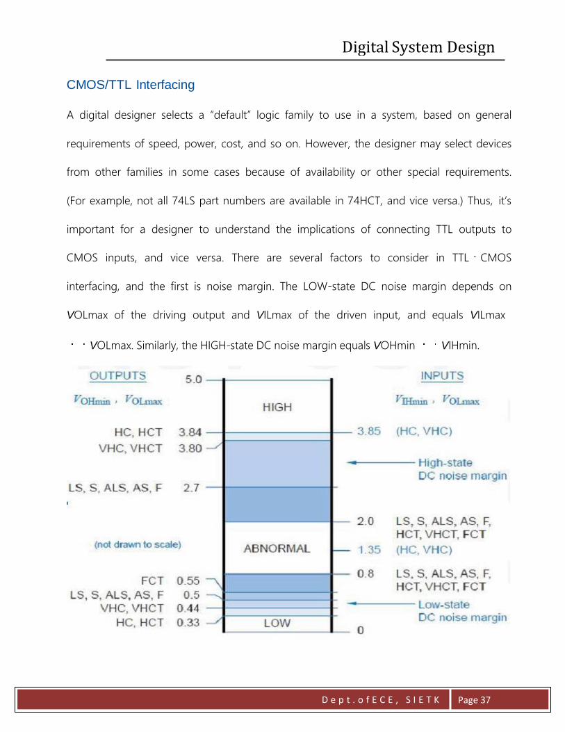
CMOS/TTL Interfacing
A digital designer selects a “default” logic family to use in a system, based on general
requirements of speed, power, cost, and so on. However, the designer may select devices
from other families in some cases because of availability or other special requirements.
(For example, not all 74LS part numbers are available in 74HCT, and vice versa.) Thus, it’s
important for a designer to understand the implications of connecting TTL outputs to
CMOS inputs, and vice versa. There are several factors to consider in TTL CMOS
interfacing, and the first is noise margin. The LOW-state DC noise margin depends on
VOLmax of the driving output and VILmax of the driven input, and equals VILmax
VOLmax. Similarly, the HIGH-state DC noise margin equals VOHmin VIHmin.

Digital System Design
D e p t . o f E C E , S I E T K Page 38
Low-Voltage CMOS Logic and Interfacing
Two important factors have led the IC industry to move towards lower powersupply
voltages in CMOS devices:
• In most applications, CMOS output voltages swing from rail to rail, so the V in the CV2f
equation is the power-supply voltage. Cutting power-supply voltage reduces dynamic
power dissipation more than proportionally.
• As the industry moves towards ever-smaller transistor geometries, the oxide insulation
between a CMOS transistor’s gate and its source and drain is getting ever thinner, and
thus incapable of insulating voltage potentials as “high” as 5 V. As a result, JEDEC, an IC
industry standards group, selected 3.3V ± 0.3V, 2.5V ± 0.2V, and 1.8V± 0.15V as the next
“standard” logic power-supply voltages. JEDEC standards specify the input and output
logic voltage levels for devices operating with these power-supply voltages.
V LVTTL and LVCMOS Logic
The relationships among signal levels for standard TTL and low-voltage CMOS devices
operating at their nominal power-supply voltages are illustrated nicely in Figure 3-85,
adapted from a Texas Instruments application note. The original, symmetric signal levels
for pure 5-V CMOS families such as HC and VHC are shown in (a). TTL-compatible
CMOS families such as HCT, VHCT, and FCT shift the voltage levels downwards for
compatibility with TTL as shown in (b). The first step in the progression of lower CMOS
power-supply voltages was 3.3 V. The JEDEC standard for 3.3-V logic actually defines

Digital System Design
D e p t . o f E C E , S I E T K Page 39
two sets of levels. LVCMOS (low-voltage CMOS) levels are used in pure CMOS
applications where outputs have light DC loads (less than 100 �A), so VOL and VOH are
maintained within 0.2 V of the power-supply rails. LVTTL (low-voltage TTL) levels, shown
in (c), are used in applications where outputs have significant DC loads, so VOL can be as
high as 0.4 V and VOH can be as low as 2.4 V. The positioning of TTL’s logic levels at the
low end of the 5-V range was really quite fortuitous. As shown in Figure 3-85(b) and (c), it
was possible to define the LVTTL levels to match up with TTL levels exactly. Thus, an
LVTTL output can drive a TTL input with no problem, as long as its output current
specifications (IOLmax, IOHmax) are respected.

Digital System Design
D e p t . o f E C E , S I E T K Page 40
5-V Tolerant Inputs
The inputs of a gate won’t necessarily tolerate voltages greater than VCC. This can easily
occur when 5-V and 3.3-V logic families in a system. For example, 5-V CMOS devices
easily produce 4.9-V outputs when lightly loaded, and both CMOS and TTL devices
routinely produce 4.0-V outputs even when moderately loaded. The maximum voltage
VImax that can be tolerated by an input is listed in the “absolute maximum ratings” section
of the manufacturer’s data sheet. For HC devices, VImax equals VCC. Thus, if an HC
device is powered by a 3.3-V supply, its cannot be driven by any 5-V CMOS or TTL
outputs. For VHC devices, on the other hand, VImax is 7 V; thus, VHC devices with a 3.3- V
power supply may be used to convert 5-V outputs to 3.3-V levels for use with 3.3-V
microprocessors, memories, and other devices in a pure 3.3-V subsystem.
Emitter-Coupled Logic:
The key to reducing propagation delay in a bipolar logic family is to prevent a gate’s
transistors from saturating. In Section 3.9.5, we learned how Schottky diodes prevent
saturation in TTL gates. However, it is also possible to prevent saturation by using a
radically different circuit structure, called current-mode logic (CML) or emitter-coupled logic
(ECL). Unlike the other logic families in this chapter, CML does not produce a large
voltage swing between the LOW and HIGH levels. Instead, it has a small voltage swing,
less than a volt, and it internally switches current between two possible paths, depending
on the output state. The first CML logic family was introduced by General Electric in 1961.

Digital System Design
D e p t . o f E C E , S I E T K Page 41
The concept was soon refined by Motorola and others to produce the still popular 10K and
100K emitter-coupled logic (ECL) families. These families are
level translator
level shifter
current-mode logic(CML)
emitter-coupled logic(ECL)
Comparison of logic families:

Digital System Design
D e p t . o f E C E , S I E T K Page 42
LLLLooooggggiiiicccc ffffaaaammmmiiiillllyyyy vvvvoooollllttttaaaaggggeeee lllleeeevvvveeeellllssss::::
IIIInnnnppppuuuutttt oooouuuuttttppppuuuutttt ssssttttaaaannnnddddaaaarrrrddddssss::::

Digital System Design
D e p t . o f E C E , S I E T K Page 43

Digital System Design
D e p t . o f E C E , S I E T K Page 44

Digital System Design
D e p t . o f E C E , S I E T K Page 45
QUESTIONS:
1.Draw the circuit diagram of two-input 10K ECL OR gate and explain its
operation.
2. List out different categories of characteristics in a TTL data sheet. Discuss
electrical and switching characteristics of 74LS00.
3. Mention the DC noise margin levels of ECL 10K family.
4. A single pull-up resistor to +5V is used to provide a constant-1 logic source
to 15 different 74LS00 inputs. What is the maximum value of this resistor?
How much high state DC noise margin can be provided in this case?
5. Design a three input NAND gate using diode logic and a transistor inverter?
Analyze the circuit with the help of transfer characteristics.
6. Explain sinking current and sourcing current of TTL output? Which of the
parameters decide the fan-out and how?
7. What are the typical parts of a TTL data sheet and discuss their importance in circuit design
8. Draw the circuit diagram of a two-input LS-TTL NOR gate. Explain the functional behavior.
9. Design a transistor circuit of 2-input ECL NOR gate. Explain the operation with the help of function table.


