Physics and Detectors Summary(WG1)
Hitoshi Yamamoto
Tohoku University
16-Oct-09, CLIC09, CERN
Apology for not covering all works!
Hitoshi Yamamoto, CLIC09 2
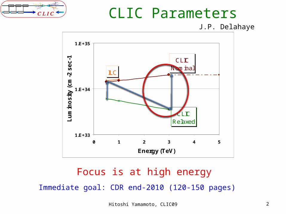
CLIC Parameters
Immediate goal: CDR end-2010 (120-150 pages)
ILC
CLICNominal
CLICRelaxed
1.E+33
1.E+34
1.E+35
0 1 2 3 4 5
Energy (TeV)
Lu
min
os
ity
(c
m-2
se
c-1
)
J.P. Delahaye
Focus is at high energy
Hitoshi Yamamoto, CLIC09 3
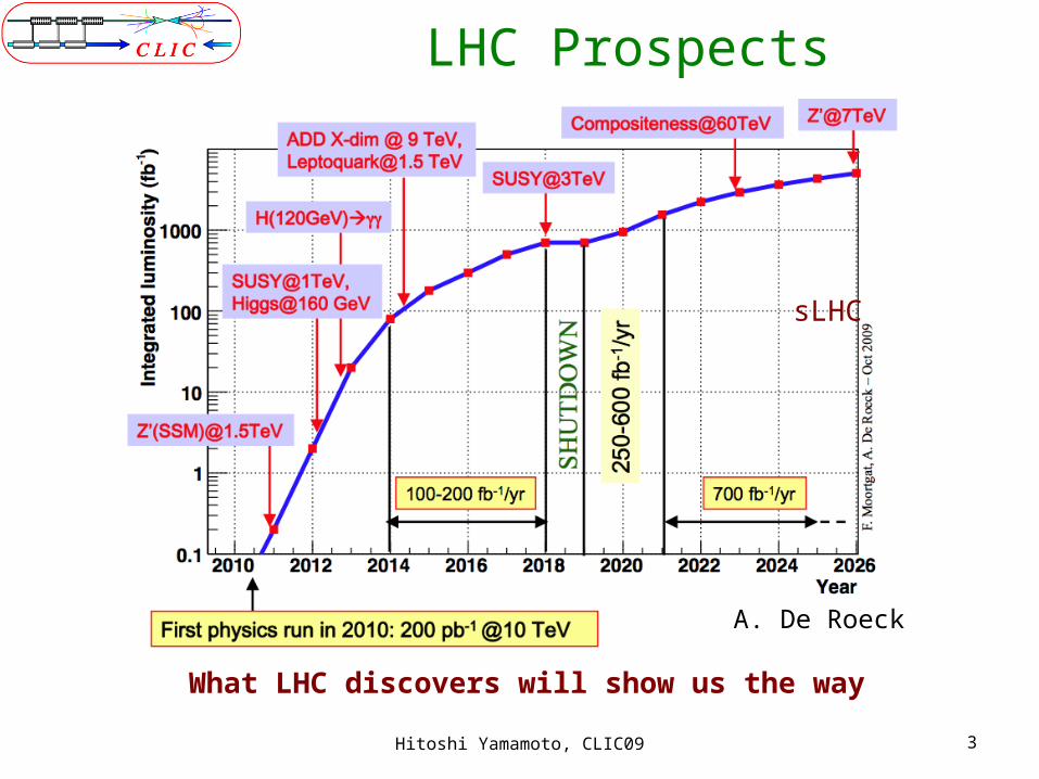
LHC Prospects
A. De Roeck
sLHC
What LHC discovers will show us the way
Hitoshi Yamamoto, CLIC09 4
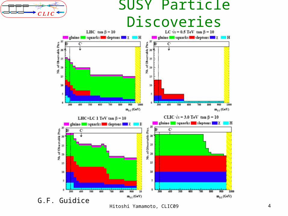
SUSY Particle Discoveries
G.F. Guidice
Hitoshi Yamamoto, CLIC09 5
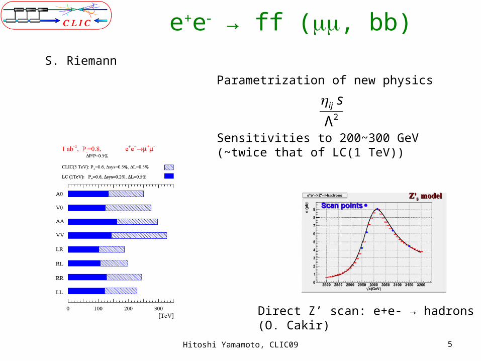
e+e- → ff (mm, bb)
S. Riemann
Parametrization of new physics
Sensitivities to 200~300 GeV(~twice that of LC(1 TeV))
€
ηij sΛ2
Direct Z’ scan: e+e- → hadrons(O. Cakir)
Hitoshi Yamamoto, CLIC09 6
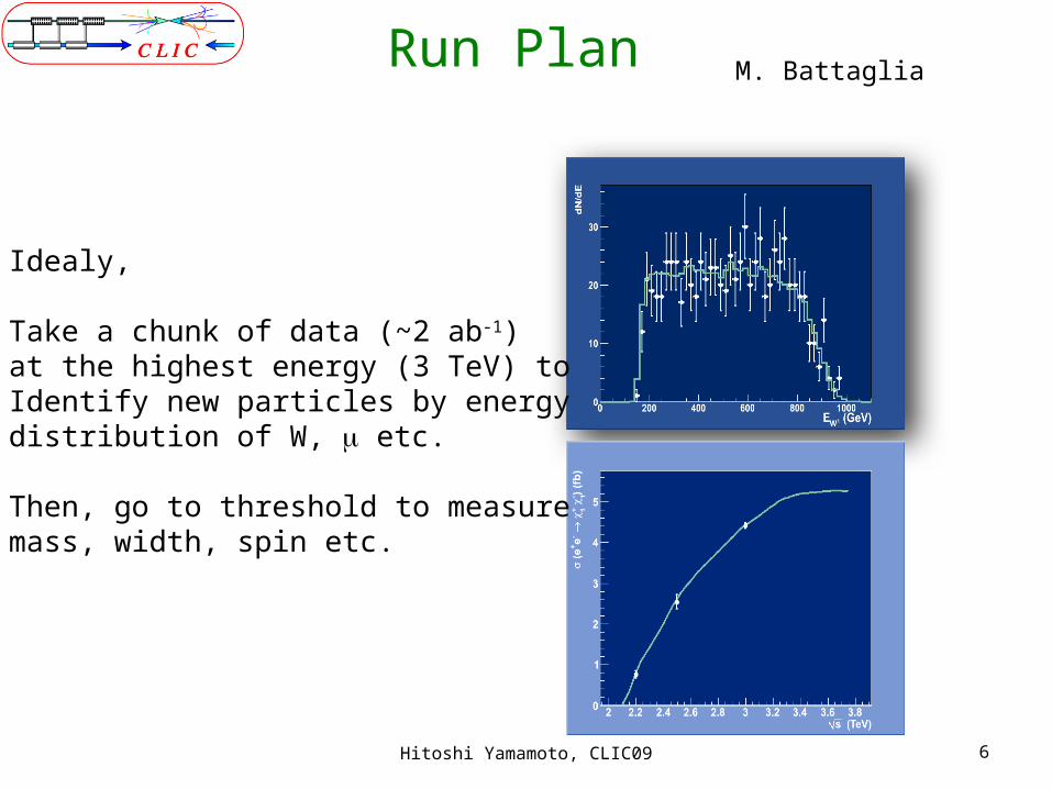
Run Plan M. Battaglia
€
e+e
−→χ
+χ
−→W
+W
−χ
0χ
0
Idealy,
Take a chunk of data (~2 ab-1) at the highest energy (3 TeV) toIdentify new particles by energy distribution of W, m etc.
Then, go to threshold to measuremass, width, spin etc.
Hitoshi Yamamoto, CLIC09 7
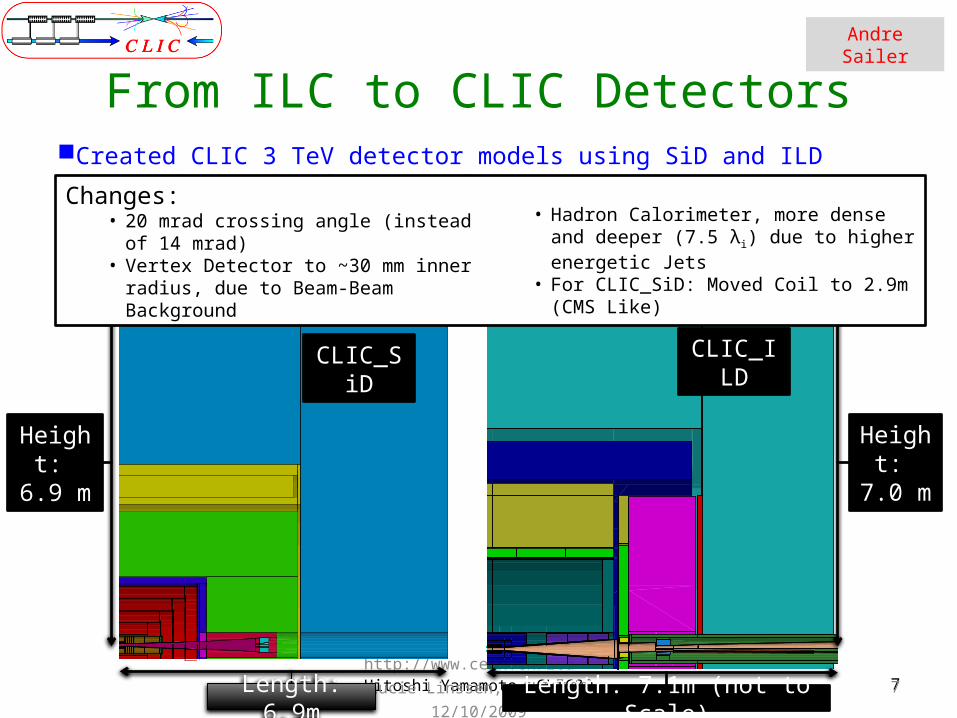
From ILC to CLIC DetectorsCreated CLIC 3 TeV detector models using SiD and ILD geometries and software
tools
7http://www.cern.ch/lcd Lucie Linssen,
CLIC'09 12/10/2009
CLIC_SiD
Length: 6.9m
CLIC_ILD
Length: 7.1m (not to Scale)
Height: 6.9 m
Height: 7.0 m
Changes:• 20 mrad crossing angle (instead of 14 mrad)• Vertex Detector to ~30 mm inner radius, due to
Beam-Beam Background
• Hadron Calorimeter, more dense and deeper
(7.5 λi) due to higher energetic Jets• For CLIC_SiD: Moved Coil to 2.9m (CMS Like)
Andre Sailer

Hitoshi Yamamoto, CLIC09 8
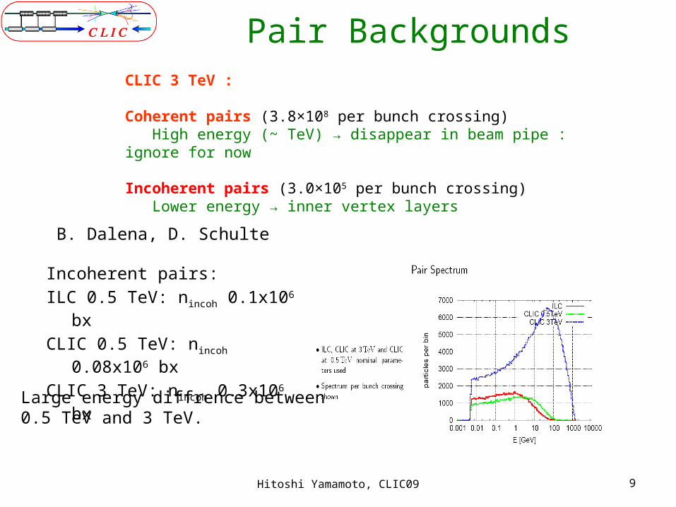
Pair Backgrounds
ILC 0.5 TeV CLIC 0.5 TeV CLIC 3 TeV
L [cm-2s-1] 2×1034 2×1034 6×1034
BX/train 2670 350 312BX sep 369 ns 0.5 ns 0.5 nsRep. rate 5 Hz 50 Hz 50 HzNbunch [109] 20 6.8 3.7
sz [mm] 300 40 40sx/sy 600 / 6 nm 200 / 2 nm 40 / 1 nm
E (bunch surface) Qb/∝ sxsz
Pt kick of pairs E ∝ sz Qb/∝ sx
Pt(CLIC 3 TeV) ~ 3 x Pt(ILC) : Expect larger pair backbrounds
Beam parameters
Hitoshi Yamamoto, CLIC09 9
Pair BackgroundsCLIC 3 TeV :
Coherent pairs (3.8×10⁸ per bunch crossing) High energy (~ TeV) → disappear in beam pipe : ignore for now
Incoherent pairs (3.0×10⁵ per bunch crossing) Lower energy → inner vertex layers
Incoherent pairs:ILC 0.5 TeV: nincoh 0.1x10⁶ bx
CLIC 0.5 TeV: nincoh 0.08x10⁶ bx
CLIC 3 TeV: nincoh 0.3x10⁶ bx
B. Dalena, D. Schulte
Large energy diffrence between0.5 TeV and 3 TeV.
Hitoshi Yamamoto, CLIC09 10
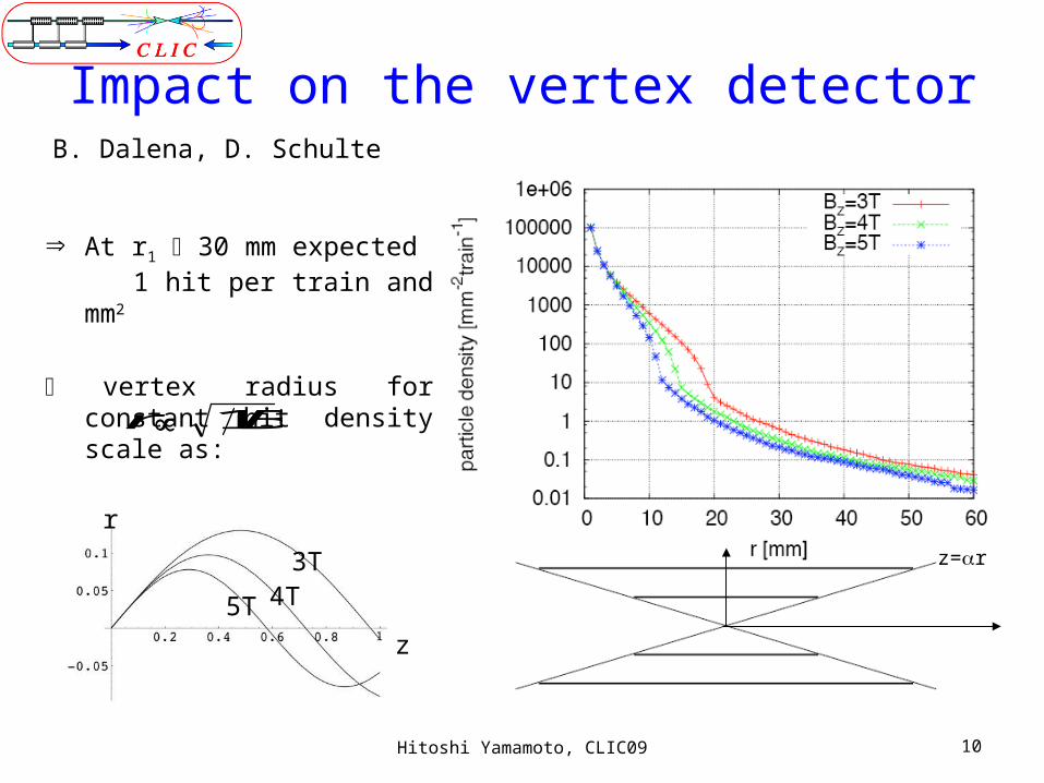
Impact on the vertex detector
Þ At r1 30 mm expected 1 hit per train and mm2
vertex radius for constant hit density scale as:
z=r
B. Dalena, D. Schulte
Bzr 1
r
z
3T4T5T
Hitoshi Yamamoto, CLIC09 11
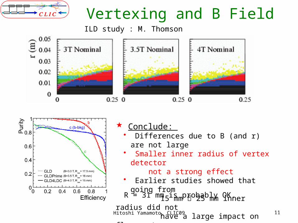
Vertexing and B FieldILD study : M. Thomson
Conclude: • Differences due to B (and r) are not large• Smaller inner radius of vertex detector
not a strong effect• Earlier studies showed that going from
15 mm 25 mm inner radius did not have a large impact on flavour tag
R = 31 mm is probably OK.
Hitoshi Yamamoto, CLIC09 12
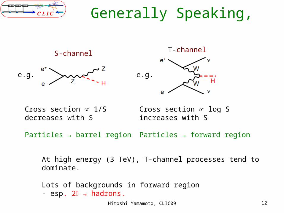
Generally Speaking,
S-channel T-channel
Cross section 1/S∝decreases with S
Particles → barrel region
Cross section log S∝increases with S
Particles → forward region
At high energy (3 TeV), T-channel processes tend todominate.
Lots of backgrounds in forward region - esp. 2g → hadrons.
e.g. e.g.
Hitoshi Yamamoto, CLIC09 13
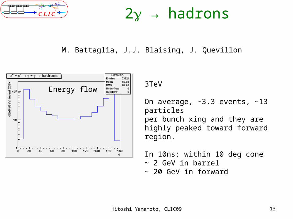
2g → hadrons
M. Battaglia, J.J. Blaising, J. Quevillon
3TeV
On average, ~3.3 events, ~13 particlesper bunch xing and they are highly peaked toward forward region.
In 10ns: within 10 deg cone~ 2 GeV in barrel~ 20 GeV in forward
Energy flow
14
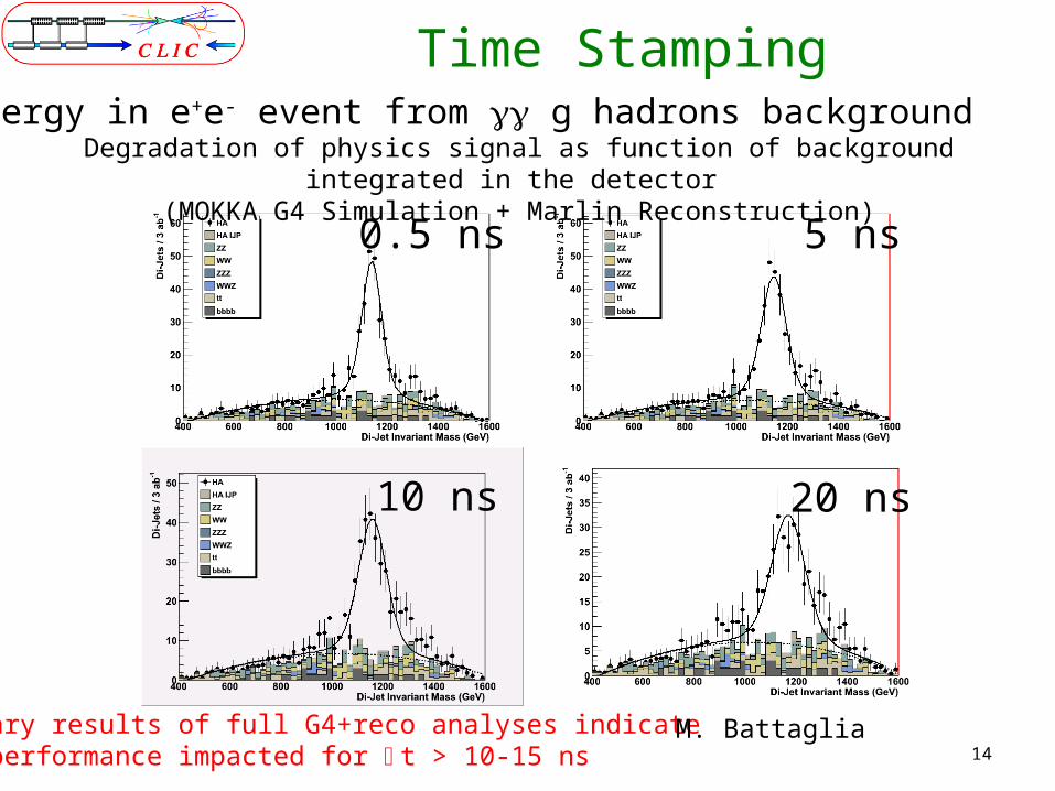
Time Stamping Energy in e+e- event from gg g hadrons background
Degradation of physics signal as function of background integrated in the detector (MOKKA G4 Simulation + Marlin Reconstruction)
Preliminary results of full G4+reco analyses indicate physics performance impacted for Dt > 10-15 ns
0.5 ns 5 ns
10 ns 20 ns
M. Battaglia
Hitoshi Yamamoto, CLIC09 15
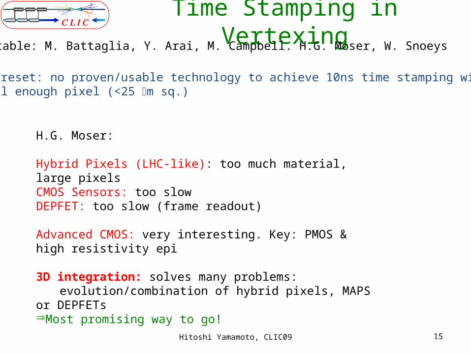
Time Stamping in VertexingRoundtable: M. Battaglia, Y. Arai, M. Campbell. H.G. Moser, W. Snoeys
H.G. Moser:
Hybrid Pixels (LHC-like): too much material, large pixelsCMOS Sensors: too slowDEPFET: too slow (frame readout)
Advanced CMOS: very interesting. Key: PMOS & high resistivity epi
3D integration: solves many problems: evolution/combination of hybrid pixels, MAPS or DEPFETs
ÞMost promising way to go!
At preset: no proven/usable technology to achieve 10ns time stamping withsmall enough pixel (<25 mm sq.)

Hitoshi Yamamoto, CLIC09 16
3D Integration (1)
> Higher integration density> Radiation tolerance> Lower power cnsumption
Test chip designed by LBNL/KEK.
Bonded by Zycube (Co.).Will be tested soon.

Hitoshi Yamamoto, CLIC09 17
3D integration (2)
Hitoshi Yamamoto, CLIC09 18
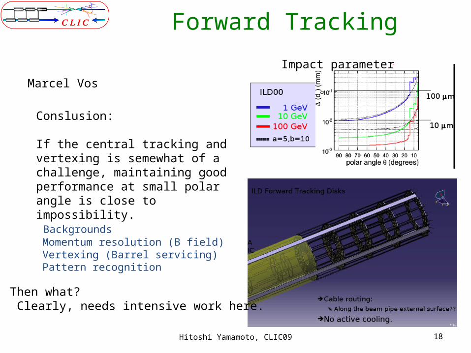
Forward Tracking
Marcel Vos
Conslusion:
If the central tracking and vertexing is semewhat of a challenge, maintaining good performance at small polar angle is close to impossibility. Backgrounds Momentum resolution (B field) Vertexing (Barrel servicing) Pattern recognition
Then what? Clearly, needs intensive work here.
Impact parameter
Hitoshi Yamamoto, CLIC09 19
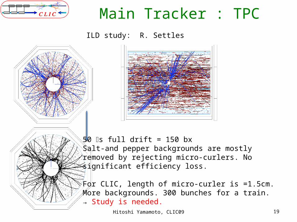
Main Tracker : TPCILD study: R. Settles
50 ms full drift = 150 bxSalt-and pepper backgrounds are mostlyremoved by rejecting micro-curlers. No significant efficiency loss.
For CLIC, length of micro-curler is =1.5cm.More backgrounds. 300 bunches for a train.→ Study is needed.

Hitoshi Yamamoto, CLIC09 20
Main Tracker : Silicon
Possibly good for time stamping.
Maybe also better suited for forwardregion Tracking. (no thick end-plate)
Can pattern recognition work in thehigh background environment?
Track finding study with realistic geometryIs now on-going. – D. Grefe

Hitoshi Yamamoto, CLIC09 21
Pixellated TPC
275 μm
Use pixel sensor instead of wire or MPGD (Micro-Pattern Gas Detector) such as MicroMEGAS or GEM.
Pad size : 1x5 mm2 to 55x55 mm2
Good spacial resolutionGood 2-track separation (<1mm)Possibly cluster counting (dE/dx)
J. Timmermans
Hitoshi Yamamoto, CLIC09 22
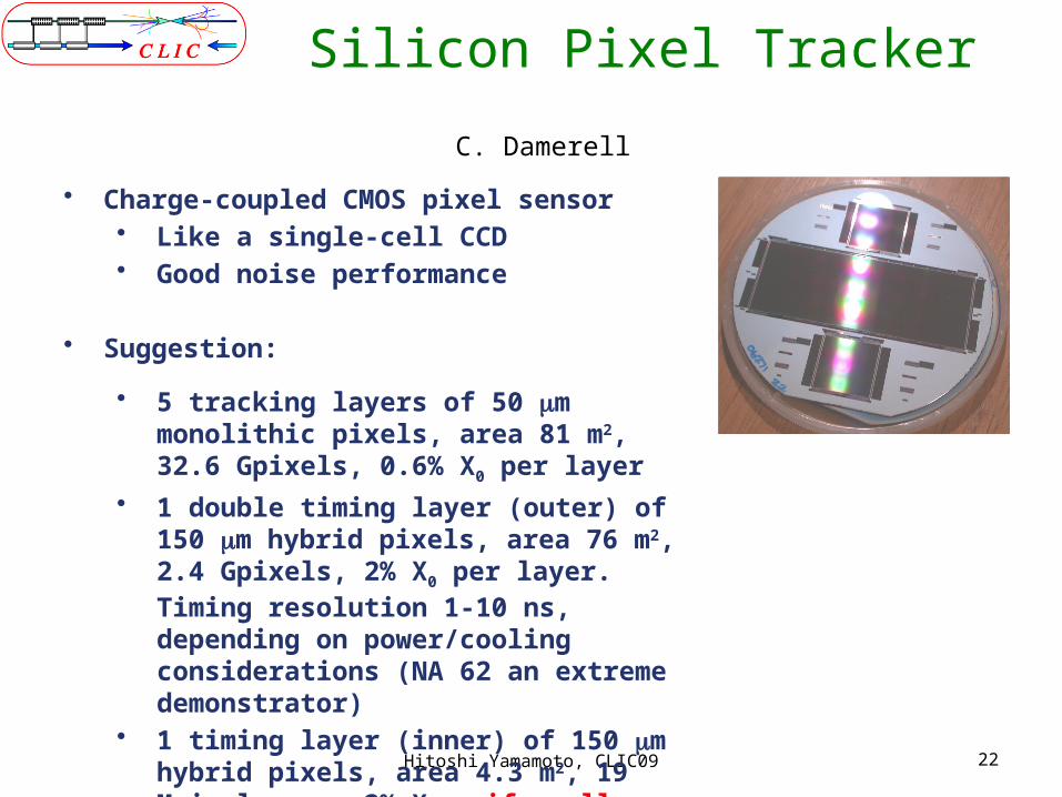
Silicon Pixel Tracker
• Charge-coupled CMOS pixel sensor• Like a single-cell CCD• Good noise performance
• Suggestion:
• 5 tracking layers of 50 mm monolithic pixels, area 81 m2, 32.6 Gpixels, 0.6% X0 per layer
• 1 double timing layer (outer) of 150 mm hybrid pixels, area 76 m2, 2.4 Gpixels, 2% X0 per layer. Timing resolution 1-10 ns, depending on power/cooling considerations (NA 62 an extreme demonstrator)
• 1 timing layer (inner) of 150 mm hybrid pixels, area 4.3 m2, 19 Mpixels, 2% X0 , if really needed
C. Damerell
Hitoshi Yamamoto, CLIC09 23
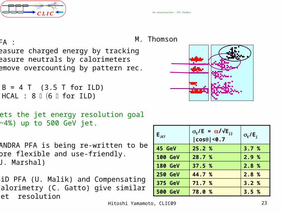
Jet reconstruction - PFA (Pandra)
EJETsE/E = a/√Ejj |cosq|<0.7
sE/Ej
45 GeV 25.2 % 3.7 %
100 GeV 28.7 % 2.9 %
180 GeV 37.5 % 2.8 %
250 GeV 44.7 % 2.8 %
375 GeV 71.7 % 3.2 %
500 GeV 78.0 % 3.5 %
PFA :Measure charged energy by trackingMeasure neutrals by calorimetersRemove overcounting by pattern rec.
B = 4 T (3.5 T for ILD)HCAL : 8 (l 6 l for ILD)
Meets the jet energy resolution goal(3~4%) up to 500 GeV jet.
M. Thomson
PANDRA PFA is being re-written to bemore flexible and use-friendly.(J. Marshal)
SiD PFA (U. Malik) and CompensatingCalorimetry (C. Gatto) give similarjet resolution
Hitoshi Yamamoto, CLIC09 24
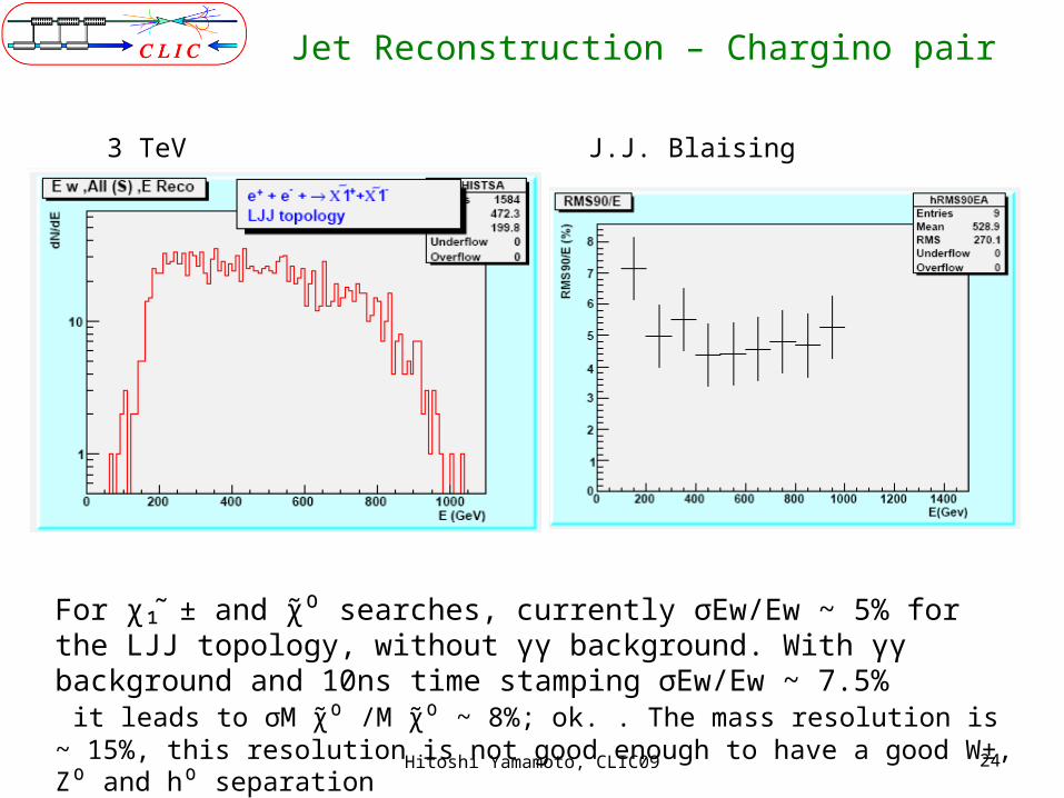
Jet Reconstruction – Chargino pair
For χ ₁̃. ± and ⁰χ̃. searches, currently σEw/Ew ~ 5% for the LJJ topology, without γγ background. With γγ background and 10ns time stamping σEw/Ew ~ 7.5% it leads to σM ⁰χ̃. /M ⁰χ̃. ~ 8%; ok. . The mass resolution is ~ 15%, this resolution is not good enough to have a good W±, Z⁰ and h⁰ separation
J.J. Blaising3 TeV

Hitoshi Yamamoto, CLIC09 25
Jet Clustering Tuning
Colors: different time stamping (0-100 ns)
J. Quevillon
€
e+e− →HA→ bbbb
Hitoshi Yamamoto, CLIC09 26
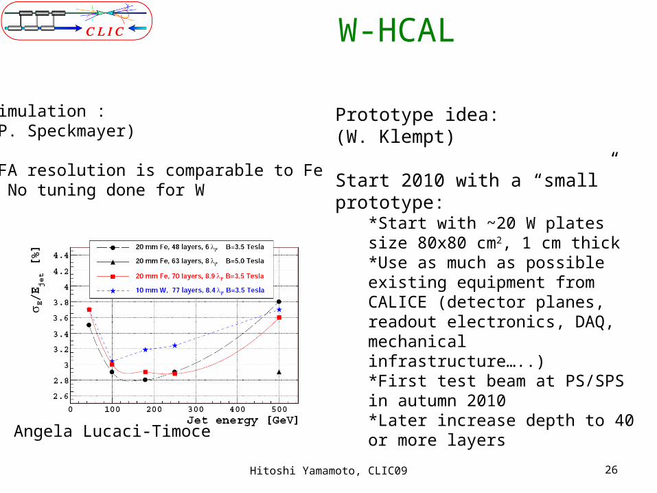
W-HCAL
Simulation :(P. Speckmayer)
PFA resolution is comparable to Fe- No tuning done for W
Angela Lucaci-Timoce
Prototype idea:(W. Klempt)
Start 2010 with a “small” prototype:*Start with ~20 W plates size 80x80 cm2, 1 cm thick*Use as much as possible existing equipment from CALICE (detector planes, readout electronics, DAQ, mechanical infrastructure…..)*First test beam at PS/SPS in autumn 2010*Later increase depth to 40 or more layers

Hitoshi Yamamoto, CLIC09 27
CALICE Beam Tests Main beam tests, using , , e beams: 2006-7
SiW ECAL + AHCAL + TCMT @ CERN 2007
Small DHCAL test @ Fermilab 2008
SiW ECAL + AHCAL + TCMT @ Fermilab 2009
Scint-W ECAL + AHCAL + TCMT @ Fermilab Standalone RPC and Micromegas tests @ CERN
2010 planned SiW ECAL + DHCAL + TCMT @ Fermilab
There is no perfect Hadron shower MC.Results are more or less consistent with MC.
D. Ward
Hitoshi Yamamoto, CLIC09 28
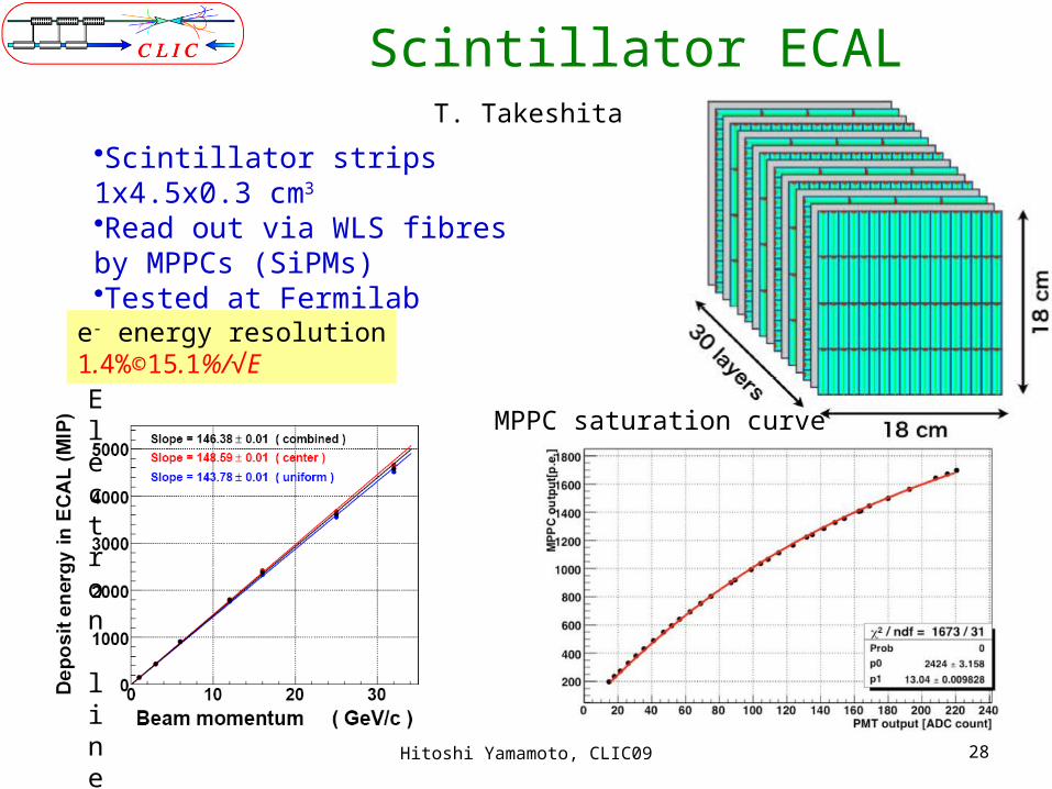
Scintillator ECALT. Takeshita
•Scintillator strips 1x4.5x0.3 cm3
•Read out via WLS fibres by MPPCs (SiPMs)•Tested at Fermilab
Electron linearity
MPPC saturation curve
e- energy resolution1.4%©15.1%/√E
Hitoshi Yamamoto, CLIC09 29
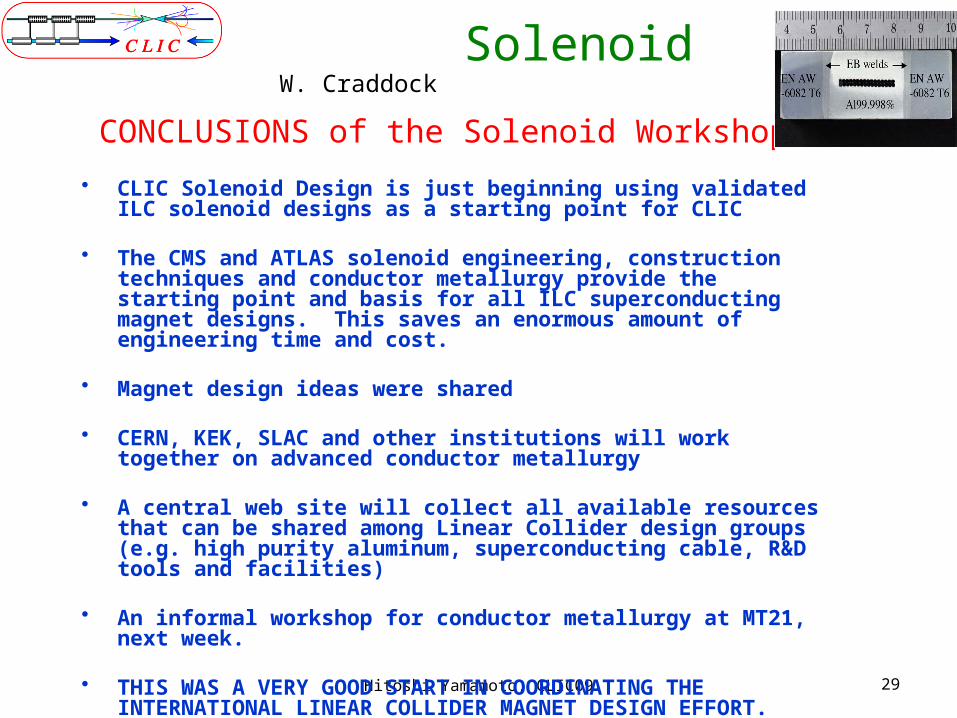
Solenoid
CONCLUSIONS of the Solenoid Workshop
• CLIC Solenoid Design is just beginning using validated ILC solenoid designs as a starting point for CLIC
• The CMS and ATLAS solenoid engineering, construction techniques and conductor metallurgy provide the starting point and basis for all ILC superconducting magnet designs. This saves an enormous amount of engineering time and cost.
• Magnet design ideas were shared
• CERN, KEK, SLAC and other institutions will work together on advanced conductor metallurgy
• A central web site will collect all available resources that can be shared among Linear Collider design groups (e.g. high purity aluminum, superconducting cable, R&D tools and facilities)
• An informal workshop for conductor metallurgy at MT21, next week.
• THIS WAS A VERY GOOD START IN COORDINATING THE INTERNATIONAL LINEAR COLLIDER MAGNET DESIGN EFFORT.
W. Craddock
Hitoshi Yamamoto, CLIC09 30
Summary
The physics potential of CLIC is impressive.The detail will, however, depends strongly on LHC outputs.
Pair and hadronic 2g backgrounds are large, and detailed full simulation studies are needed forVertexing detector configurationChoice of TPC vs Silicon (or others)Time stamping needs for each subdetector
Dominant t-channels (signal and backgrounds) pose severe challenge for the forward region
Much work has been done, but much more to be done. Collaboration between CLIC and ILC is critical .

Hitoshi Yamamoto, CLIC09 31


