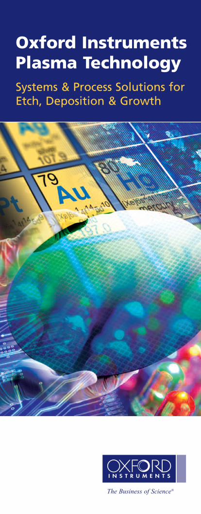
Oxford InstrumentsPlasma TechnologySystems & Process Solutions forEtch, Deposition & Growth
The Business of Science®
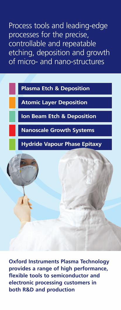
Process tools and leading-edgeprocesses for the precise,controllable and repeatableetching, deposition and growthof micro- and nano-structures
Plasma Etch & Deposition
Atomic Layer Deposition
Ion Beam Etch & Deposition
Nanoscale Growth Systems
Hydride Vapour Phase Epitaxy
Oxford Instruments Plasma Technologyprovides a range of high performance,flexible tools to semiconductor andelectronic processing customers in both R&D and production
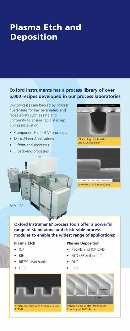
Plasma Etch andDeposition
Si step coverage with 170nm Si2 TEOSPECVD
Plasma Etch
• ICP
• RIE
• RIE/PE switchable
• DRIE
Plasma Deposition
• PECVD and ICP CVD
• ALD (PE & thermal)
• DLC
• PVD
Oxford Instruments’ process tools offer a powerfulrange of stand-alone and clusterable processmodules to enable the widest range of applications:
Oxford Instruments has a process library of over6,000 recipes developed in our process laboratories
Our processes are backed by processguarantees for key parameters andrepeatability such as rate and uniformity to ensure rapid start-upduring installation.
• Compound Semi (III-V) processes
• Micro/Nano Applications
• Si front-end processes
• Si back-end processes
ICP etching of InP withCH4/H2/Cl2 chemistry
Low stress SiN film (400nm)
Polycrystaline Si etch 34nm gates Courtesy of AMO Aachen
System100
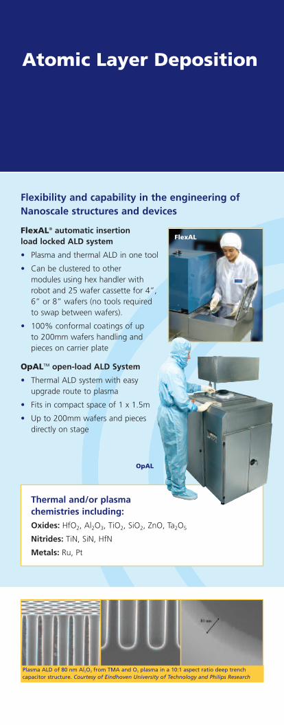
Thermal and/or plasma chemistries including:
Oxides: HfO2, Al2O3, TiO2, SiO2, ZnO, Ta2O5
Nitrides: TiN, SiN, HfN
Metals: Ru, Pt
Atomic Layer Deposition
Flexibility and capability in the engineering ofNanoscale structures and devices
FlexAL® automatic insertion load locked ALD system
• Plasma and thermal ALD in one tool
• Can be clustered to other modules using hex handler withrobot and 25 wafer cassette for 4”,6” or 8” wafers (no tools requiredto swap between wafers).
• 100% conformal coatings of up to 200mm wafers handling andpieces on carrier plate
OpALTM open-load ALD System
• Thermal ALD system with easyupgrade route to plasma
• Fits in compact space of 1 x 1.5m
• Up to 200mm wafers and piecesdirectly on stage
Plasma ALD of 80 nm Al2O3 from TMA and O2 plasma in a 10:1 aspect ratio deep trenchcapacitor structure. Courtesy of Eindhoven University of Technology and Philips Research
FlexAL
OpAL
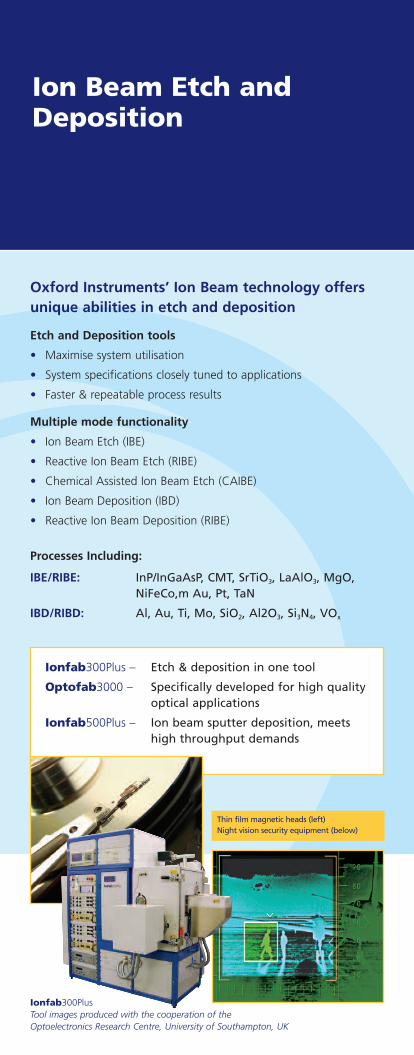
Thin film magnetic heads (left)Night vision security equipment (below)
Ion Beam Etch andDeposition
Oxford Instruments’ Ion Beam technology offersunique abilities in etch and deposition
Etch and Deposition tools
• Maximise system utilisation
• System specifications closely tuned to applications
• Faster & repeatable process results
Multiple mode functionality
• Ion Beam Etch (IBE)
• Reactive Ion Beam Etch (RIBE)
• Chemical Assisted Ion Beam Etch (CAIBE)
• Ion Beam Deposition (IBD)
• Reactive Ion Beam Deposition (RIBE)
Ionfab300Plus – Etch & deposition in one tool
Optofab3000 – Specifically developed for high qualityoptical applications
Ionfab500Plus – Ion beam sputter deposition, meetshigh throughput demands
Processes Including:
IBE/RIBE: InP/InGaAsP, CMT, SrTiO3, LaAlO3, MgO,NiFeCo,m Au, Pt, TaN
IBD/RIBD: Al, Au, Ti, Mo, SiO2, Al2O3, Si3N4, VOx
Ionfab300Plus Tool images produced with the cooperation of theOptoelectronics Research Centre, University of Southampton, UK
Nanoscale Growth
Nanoscale features can be formed by growthtechniques (‘bottom up’) and etching (‘top down’).The NanofabTM system is targeted at growth tosatisfy the nanotechnology markets
Nanoscale growth processes encompass:
• Nanotubes/nanowires
• Nanoscale thin films
Nanofab700 & Nanofab800Agile
• Can accommodate variable sample sizes up to 200 mm waferwith excellent temperature uniformity
• Compatible growth of nanotubes and nanowires with flexibletemperature up to 700°C and 800°C respectively
• Nanofab700 is compatible with Oxygen and other processatmospheres
• Nanofab800Agile can give agile heating and cooling for rapidturn round with its exceptional electrode features
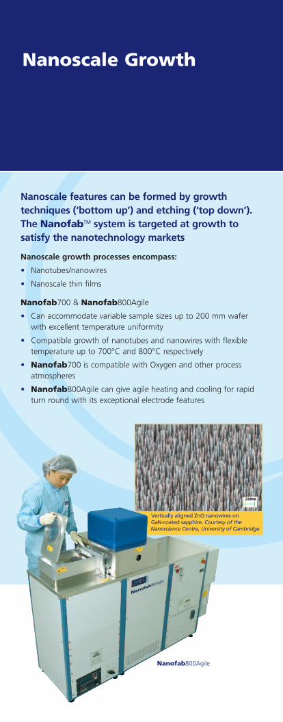
Nanofab800Agile
Vertically aligned ZnO nanowires on GaN-coated sapphire. Courtesy of theNanoscience Centre, University of Cambridge
Hydride Vapour PhaseEpitaxy
A world leader in the development of Hydride VapourPhase Epitaxy (HVPE) processes and techniques forthe production of novel compound semiconductors,such as GaN, AlN, AlGaN, InN and InGaN
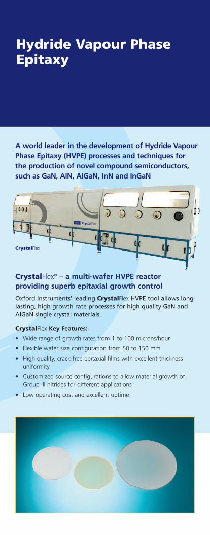
CrystalFlex® – a multi-wafer HVPE reactorproviding superb epitaxial growth control
Oxford Instruments’ leading CrystalFlex HVPE tool allows longlasting, high growth rate processes for high quality GaN andAlGaN single crystal materials.
CrystalFlex Key Features:
• Wide range of growth rates from 1 to 100 microns/hour
• Flexible wafer size configuration from 50 to 150 mm
• High quality, crack free epitaxial films with excellent thicknessuniformity
• Customized source configurations to allow material growth ofGroup III nitrides for different applications
• Low operating cost and excellent uptime
CrystalFlex
Proven Cassette to Cassettehandling technology with fullwafer tracking is available forboth single wafer and multi-wafer platen configurations
HBLED
Production processes and tools for HBLEDmanufacture offering exceptional Batch and SingleWafer capability
• Family of batch productionsolutions
- PECVD Batch Deposition
- ICP Batch Etch
• Single wafer processes andsystems
- ICP Etch
- ICPCVD and PECVD
• Highest possible throughput
• Proven e-chuck clampingcapability
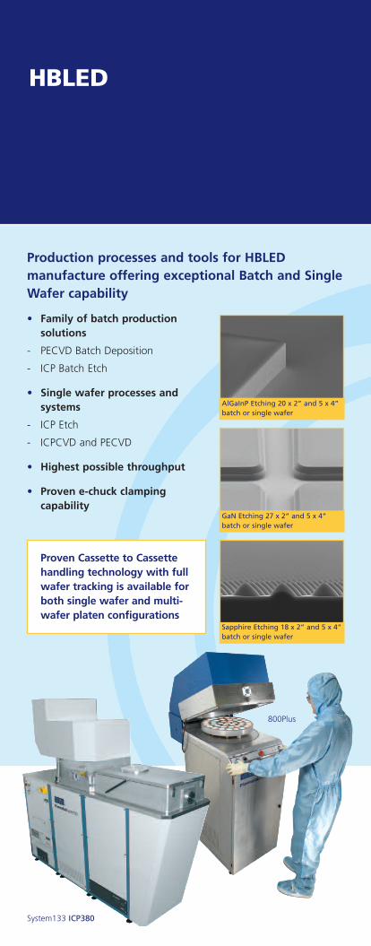
AlGaInP Etching 20 x 2” and 5 x 4”batch or single wafer
GaN Etching 27 x 2” and 5 x 4”batch or single wafer
Sapphire Etching 18 x 2” and 5 x 4”batch or single wafer
800Plus
System133 ICP380
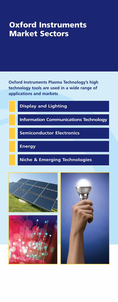
Oxford InstrumentsMarket Sectors
Oxford Instruments Plasma Technology’s hightechnology tools are used in a wide range ofapplications and markets
Display and Lighting
Information Communications Technology
Energy
Semiconductor Electronics
Niche & Emerging Technologies

The Business of Science®
As part of Oxford Instruments’environmental policy this brochurehas been printed on FSC paper
www.oxford-instruments.com
WorldwideService andSupport
Oxford Instruments is committed to supporting ourcustomers’ success. We recognise that this requiresworld class products complemented by world classsupport. Our global service force is backed byregional offices, offering rapid support whereveryou are in the world.
We can provide:
• Tailored service agreements to meet your needs
• Comprehensive range of structured training courses
• Immediate access to genuine spare parts andaccessories
• System upgrades and refurbishments
Email: [email protected]: +44 (0) 1934 837000 (Head Office)
For worldwide office contact information please visit our website


