doi: 10.1002/cssc.201000416 solar water splitting...
TRANSCRIPT

DOI: 10.1002/cssc.201000416
Solar Water Splitting: Progress Using Hematite (a-Fe2O3)PhotoelectrodesKevin Sivula,* Florian Le Formal, and Michael Gr�tzel[a]
432 � 2011 Wiley-VCH Verlag GmbH & Co. KGaA, Weinheim ChemSusChem 2011, 4, 432 – 449

1. Introduction
Energy from the Sun can easily provide enough power for allof our energy needs if it can be efficiently harvested. Whilethere already exist a number of devices that can capture andconvert electromagnetic energy, the most common—a photo-voltaic cell—produces electricity, which must be used immedi-ately or stored in a secondary device such as a battery or a fly-wheel. A more elegant, practical, and potentially more efficientroute to storing solar power is to convert the electromagneticenergy directly into chemical energy in the form of molecularbonds, analogous to the photosynthesis process exploited bynature.[1] Biologic photosynthesis effectively rearranges elec-trons in H2O and CO2 to store solar energy in the form of car-bohydrates. However, the extremely low overall efficiency thatnatural photosynthesis exhibits implies the requirement of vastamounts land and farming resources to meet our energy de-mands.[2–3] Because of this, artificial photosynthetic routes in-cluding photoelectrochemical (PEC) and photocatalytic (PC)solar energy conversion have been intensely investigated overthe last four decades. Given the abundance of H2O on Earth,the water splitting reaction, H2O!1=2O2 + H2 (E0 = 1.23 V), is themost appealing pathway for artificial photosynthesis. Indeedsolar water splitting would form the basis for a sustainable hy-drogen-based energy economy.
A distinction can be made between the different approachesto artificial photosynthesis : PC water splitting systems use adispersed material in pure water and accordingly produce hy-drogen and oxygen homogeneously throughout the solution.This approach is under examination with both inorganic col-loid materials[4–5] and molecular complexes.[6] In contrast, PECsystems employ photoactive materials as electrodes. As in con-ventional water electrolysis, oxidation (O2 evolution) occurs atthe anode, reduction (H2 evolution) occurs at the cathode, andan aqueous electrolyte completes the current loop betweenthe electrodes and an external circuit. One or both of the elec-trodes can be a photoactive semiconductor, in which a space-charge (depletion) layer is formed at the semiconductor/liquidjunction (SCLJ). Upon irradiation, photogenerated carriers areseparated by the space-charge field and the minority carriers(holes for an n-type photoanode and electrons for a p-typephotocathode) travel to the SCLJ to perform one half of the
water splitting reaction. The schematic for an n-type photo-anode is shown in Figure 1 a. The advantage of the PEC routeis that it allows the spatially separate production, and thereforecollection, of H2 and O2.
Photoelectrochemical (PEC) cells offer the ability to convertelectromagnetic energy from our largest renewable source, theSun, to stored chemical energy through the splitting of waterinto molecular oxygen and hydrogen. Hematite (a-Fe2O3) hasemerged as a promising photo-electrode material due to itssignificant light absorption, chemical stability in aqueous envi-ronments, and ample abundance. However, its performance asa water-oxidizing photoanode has been crucially limited bypoor optoelectronic properties that lead to both low light har-vesting efficiencies and a large requisite overpotential for pho-toassisted water oxidation. Recently, the application of nano-structuring techniques and advanced interfacial engineeringhas afforded landmark improvements in the performance of
hematite photoanodes. In this review, new insights into thebasic material properties, the attractive aspects, and the chal-lenges in using hematite for photoelectrochemical (PEC) watersplitting are first examined. Next, recent progress enhancingthe photocurrent by precise morphology control and reducingthe overpotential with surface treatments are critically detailedand compared. The latest efforts using advanced characteriza-tion techniques, particularly electrochemical impedance spec-troscopy, are finally presented. These methods help to definethe obstacles that remain to be surmounted in order to fullyexploit the potential of this promising material for solar energyconversion.
Figure 1. a) Energy diagram for photoelectrochemical water splitting with ann-type photoanode (hematite) performing the oxygen evolution (oxidation)reaction and a cathode performing the hydrogen evolution (reduction) reac-tion. The photoanode bandgap, Eg, flat band potential, Vfb, and the appliedbias, Vb, are indicated. b) Photoanode/photovoltaic water splitting tandemcell concept, shown with a dye-sensitized solar cell (DSC).
[a] Dr. K. Sivula, F. Le Formal, Prof. Dr. M. Gr�tzelInstitute of Chemical Sciences and Engineering�cole Polytechnique F�d�rale de LausanneStation 6, 1015 Lausanne (Switzerland)Fax: (+ 41) 21 693 41 11E-mail : [email protected]
ChemSusChem 2011, 4, 432 – 449 � 2011 Wiley-VCH Verlag GmbH & Co. KGaA, Weinheim www.chemsuschem.org 433
Solar Water Splitting: Progress Using a-Fe2O3 Photoelectrodes

Despite the difference between PC and PEC water splitting,the requirements of the materials employed are essentially thesame, and ever since the seminal demonstration of PEC watersplitting with TiO2,[7–8] scientists and engineers have sustaineda vigorous search for a material combining the essential re-quirements: a small semiconductor bandgap for ample solarlight absorption, conduction and valence band energies thatstraddle the water oxidization and reduction potentials, highconversion efficiency of photogenerated carriers to the watersplitting products, durability in aqueous environments, andlow cost. However, to date no single semiconducting material
has been found to meet all of these requirements.[1] Transitionmetal oxides such as TiO2 possess adequate stability but onlyabsorb a small fraction of solar illumination due to their largeband gap (Eg = 3.2 eV for anatase TiO2). Many other semicon-ductors have smaller bandgaps and appropriate energy levels,such as InP (Eg = 1.3 eV); however, they exhibit poor stability inaqueous environments.[9] While much work continues to focuson identifying an ideal material using combinatorial[10] andab initio (density-functional theory)[11–12] approaches, an alter-native approach borrows again from biologic photosynthesis,which uses two photosystems in tandem.
By relaxing the constraint that only one material (whosebandgap energy levels straddle the water redox potentials)can be used, combinations of complementary semiconductorscan be employed.[13] For example, a photoanode and a photo-cathode or a photoelectrode and a photovoltaic (PV) devicecan be used in tandem to afford overall solar water splittingwith two or more photon absorption events. Systems deliver-ing a record solar-to-hydrogen (STH) efficiency over 12 % havebeen demonstrated using III–V semiconductor materials withthis approach, but their cost and stability remain major disad-vantages.[14] Alternatively, inexpensive and stable oxide photo-anodes, such as WO3 (Eg = 2.6 eV),[15–16] with conduction bandedges too-low in energy to reduce water, can receive an exter-nal bias from an economical PV device such as a dye-sensitizedsolar cell (DSC), which harvests solar photons not absorbed bythe semi-transparent photoanode. This photoanode/DSC con-cept is shown in Figure 1 b. Using a WO3 photoanode it hasdemonstrated an overall water splitting efficiency of 4.5 %.[1]
Unfortunately due to its relatively large bandgap and expectedkinetic losses, a maximum of only 8 % STH is possible withWO3.[17]
However, a tandem water splitting device holds great prom-ise if a photoanode can be developed that combines sufficientlight absorption, stability, and performance using raw materialsof ample availability and low cost. Iron(III) oxide, Fe2O3, is apromising material in light of these requirements. With a po-tential to convert 16.8 % of the sun’s energy into hydrogen,[17]
it has been extensively examined for application to solar watersplitting. In this review the advantageous properties of Fe2O3
as well as the challenges it presents to photoelectrochemicalwater splitting are presented. The most recent efforts at con-trolling water oxidation at the SCLJ, improving photon harvest-ing by nanostructuring, and increasing the understanding ofthis promising material for solar energy conversion are criticallyexamined.
2. Hematite as a Promising Material
Iron is the fourth most common element in the earth’s crust(6.3 % by weight) and because iron is readily oxidized in air tothe ferrous (+2) and ferric (+3) states, iron oxide is ubiquitous.For example, both the geological formations in the southwestUnited States (see frontispiece) and a rusty automobile fendertake their distinctive red-brown color from the presence ofiron oxides. These chromatic characteristics also exemplify ironoxide’s ability to absorb solar irradiation. This coupled with its
Dr. Kevin Sivula is a native of Minneap-
olis, MN (USA). He completed his
B.Ch.E degree at the University of Min-
nesota in 2002, and then went on to
investigate materials for bulk-hetero-
junction photovoltaic devices at UC
Berkeley under the supervision of Prof.
Jean Fr�chet. In 2007 he joined the
Laboratory of Photonics and Interfaces
at EPFL to further study solar energy
conversion. He is now leading the re-
search activities of PECHouse, a Swiss
centre of excellence devoted to the development of materials for
solar water splitting.
Florian Le Formal was born in France
in 1984. He obtained his M.Sc. in mate-
rials science at the European School of
Chemistry, Polymers and Material Sci-
ence in Strasbourg (France, ECPM). He
is a currently a PhD student in the
Laboratory of Photonics and Interfaces
at EPFL. As a main topic, he is studying
photo-electrochemical water splitting
using hematite photoanodes. His
major research interests are the photo-
chemistry and the electrochemistry of
metal oxide semiconductors.
Prof. Dr. Michael Gr�tzel directs the
Laboratory of Photonics and Interfaces
at EPFL. Here he has pioneered re-
search on energy and electron transfer
reactions in mesoscopic materials and
their application in solar energy con-
version systems, optoelectronic devi-
ces and lithium ion batteries. He re-
ceived his doctorate in Natural Science
from the Technical University of Berlin,
and has since been awarded honorary
doctorates from the Universities of
Delft, Uppsala, and Turin. He is a member of the Swiss Chemical
Society, a fellow of the Royal Society of Chemistry, and an honorary
member of the Soci�t� Vaudoise de Sciences Naturelles.
434 www.chemsuschem.org � 2011 Wiley-VCH Verlag GmbH & Co. KGaA, Weinheim ChemSusChem 2011, 4, 432 – 449
K. Sivula et al.

abundance and non-toxicity make iron oxide a particularly at-tractive material for use in solar energy conversion. Since theferrous and ferric forms of iron are separated by a relativelysmall energy difference, many well-defined crystalline forms ofiron oxide and oxyhydroxide exist in nature. The distinct prop-erties of all of the iron oxides are comprehensively presentedin a recent book by Cornell and Schwertmann.[18] In this sec-tion, we present a brief overview and the latest insights intothe important and unique properties of the most importantiron oxide for solar energy conversion, a-Fe2O3 (hematite), andlook at the seminal efforts to use this material in PEC watersplitting.
2.1 Overview of properties
2.1.1 Crystalline and magnetic structure
Hematite is the most thermodynamically stable form of ironoxide under ambient conditions and as such, it is also themost common form of crystalline iron oxide. The iron andoxygen atoms in hematite arrange in the corundum structure,which is trigonal-hexagonal scalenohedral (class 3 2/m) withspace group R-3c, lattice parameters a = 5.0356 �, c =
13.7489 �, and six formula units per unit cell.[18] It is easy to un-derstand hematite’s structure based on the packing of theanions, O2�, which are arranged in a hexagonal closed-packedlattice along the [001] direction. The cations (Fe3+) occupy thetwo-thirds of the octahedral interstices (regularly, with twofilled followed by one vacant) in the (001) basal planes, andthe tetrahedral sites remain unoccupied. The arrangement ofcations can also be thought of producing pairs of FeO6 octahe-dra that share edges with three neighboring octahedra in thesame plane and one face with an octahedron in an adjacentplane in the [001] direction (Figure 2). The face-sharing is re-sponsible for a trigonal distortion of the octahedra as the prox-imal iron atoms are repelled to optimize the crystal’s Madelungenergy. Consequently, hematite exhibits a C3v symmetry and
there are two different Fe�O bond lengths, as illustrated inFigure 2. However, the electronic structures of the distortedFeO6 octahedral are thought to be similar to undistorted clus-ters.[18]
The arrangement of the oxygen anions and the high-spin(d5) cations naturally affect the orientation of the iron atoms’spin magnetic moment and thus the observed bulk magneticproperties. The diverse magnetic properties of all the iron(III)oxides have been recently reviewed.[20] In brief, hematite is an-tiferromagnetic at temperatures below 260 K and a weak (par-asitic) ferromagnet at room temperature. The latter is due tothe ferromagnetic coupling of the spins within the (001) basalplanes and antiferromagnetic coupling between iron layersalong the [001] direction.[21] Here the trigonal distortion of theFeO6 octahedra produces a slightly canted (about 58) spin ar-rangement, causing the destabilization of their perfectly anti-parallel arrangement (parasitic ferromagnetism). While themagnetic properties of hematite are not particularly pertinentto its photoelectrochemical performance, the iron spin config-uration does influence the optoelectronic and carrier transportproperties of hematite. These attributes should be properly un-derstood for its application as a semiconductor for solar watersplitting. Decades of research have passed scrutinizing themechanisms of charge transport and light absorption, andwhile hematite is still not completely understood, much prog-ress has been made.
2.1.2 Optoelectronic characteristics
The absorption of photons by hematite begins in the near-in-frared spectral region where weak absorption bands (with ab-sorption coefficients, a, of the order 103 cm�1) are due to d–dtransition states between electron energy levels of the Fe3+
ion, which are split by an intrinsic crystal field.[22] While photo-excitation of hematite at these wavelengths has been shownin one case to increase its conductivity,[23] sustained photocur-rent is not observed in a photoelectrochemical system upon ir-radiation below the bandgap energy, Eg (which, depending onthe method of preparation of hematite, is usually reported tobe between 1.9 and 2.2 eV corresponding to l= 650 to560 nm).[24] The absorption coefficient of pure hematite in-creases abruptly at the bandgap energy, and further up theelectromagnetic spectrum a continues to increase with addi-tional absorption features having been observed centered on2.4, 3.2 and 5.8 eV (with a on the order of 105 cm�1) in samplesof polycrystalline hematite.[25] Hematite’s strong absorption ofyellow to ultraviolet photons in the visible region and trans-mission of orange to infrared photons gives it a characteristicred color. However, its fairly uniform reflectivity as a functionof visible light wavelength gives specular hematite a metallicappearance.
Since the electronic nature of the bandgap in hematite is ofgreat interest to understand its performance as a material forsolar energy conversion, much work has focused on thisaspect. The Tauc analysis of the bandgap absorption onset,which assumes that the energy bands are parabolic with re-spect to the crystal momentum, most frequently indicates an
Figure 2. The unit cell (left) of hematite shows the octahedral face-sharingFe2O9 dimers forming chains in the c direction. A detailed view (right) of oneFe2O9 dimer shows how the electrostatic repulsion of the Fe3+ cations pro-duce long (light grey) and short (dark grey) Fe�O bonds. Reprinted with per-mission from [19]. Copyright 2010 American Chemical Society.
ChemSusChem 2011, 4, 432 – 449 � 2011 Wiley-VCH Verlag GmbH & Co. KGaA, Weinheim www.chemsuschem.org 435
Solar Water Splitting: Progress Using a-Fe2O3 Photoelectrodes

indirect (phonon-assisted) bandgap transition.[26] However, afew recent reports of a direct bandgap in hematite have beenattributed to quantum size-effects.[27–28] The initial orbital as-signments of the bandgap suggested it was due to an indirecttransition of Fe3+ d–d origin,[23, 29] and that a stronger directtransition involving a charge transfer from an O 2p orbital toFe 3d did not occur until 3.2 eV.[29] This led to the hypothesisthat two different types of p-type charge carriers (holes) couldbe produced in hematite, depending on the excitation mecha-nism, and were responsible for the observed difference in pho-toelectrochemical (PEC) performance as a function of wave-length.[30–31] However, the most recent ab initio calculations todetermine the electronic structure of hematite by the Hartree–Fock approach[32] and density functional theory with a localspin-density approximation and coulomb correlation[33–34] bothpredict that the highest occupied energy states are primarilyO p in character and the lowest unoccupied states are from anempty Fe d band. This conclusion is also supported by soft-X-ray (O K-edge) absorption and emission spectroscopy, which,when compared to photoemission spectra from configuration-interaction FeO6 cluster calculations, confirm that the valenceband is at least strongly hybridized and indicates further that itis mostly of O 2p character.[35] These latest results not only sug-gest that pure stoichiometric hematite is a charge transfer in-sulator, and not a Mott–Hubbard type insulator—a detail thataffects conduction models—but also contradicts the sugges-tion that two types of holes, originating from different transi-tions, could cause different PEC behavior.
2.1.3 Carrier transport
For use as a photoelectrode the efficient transport of majoritycharge carriers in hematite is essential. The earliest work byMorin on pure sintered polycrystalline samples describes verylow electrical conductivities (ca. 10�14 W�1 cm�1),[36] conductionelection concentrations of 1018 cm�3 at 1000 Kelvin, and an ac-tivation-energy type electron mobility on the order of10�2 cm2 V�1 s�1.[37] Studies on pure single-crystals showed con-ductivities below 10�6 W�1 cm�1 and were deemed unsuitablefor further electronic characterization.[38] These unusually smallvalues obliged electrical conduction to be explained by Fe3+/Fe2+ valence alternation on spatially localized 3d orbitals. Mod-eling studies have had success matching empirical data by de-scribing the conduction mechanism with a small polaronmodel that includes the effect of the larger size of the Fe2+ ionand the associated lattice distortion (polaron).[39–40] Conductionof electrons or holes are then best described by the hoppingof polarons with an activation energy. This mechanism causesthe mobility of carriers to increase with increased temperature,as the transport is phonon-assisted.[41] The localized electron-small polaron model has been supported by further experi-mental results including pulse radiolysis[42] and femtosecondlaser spectroscopy on nanoparticles.[43]
Further studies of hematite single crystals identified a highlyanisotropic electron transport with conduction along the ironbilayer (001) basal plane up to four orders of magnitude great-er than perpendicular directions (parallel to [001]).[44–45] This
discrepancy cannot be explained by the proximity of iron cat-ions alone, as the shortest Fe-Fe distances are actually alongthe [001] direction.[46] However the anisotropic conductivitycan be classically explained considering Hund’s rule and themagnetic structure of hematite. The ferromagnetic coupling ofthe spins in the (001) basal planes and antiferromagnetic cou-pling along the [001] direction create an environment whereelectrons can move (n-type conductivity) within the iron bilay-ers (an environment of parallel spins) but are forbidden to hopacross the oxygen planes to an iron bilayer with the oppositespins. As such, conduction in the [001] direction could only in-volve the movement of holes in the form of Fe3+!Fe4+ elec-tron transfer. This process is significantly slower in hematite.[41]
While this classical explanation is generally accepted, recent abinitio electron structure calculations combined with electrontransfer (Marcus) theory have correctly predicted the largetransport anisotropy in hematite, but suggested it arises fromthe slowness of both hole and electron transport across basaloxygen planes.[21] This explanation does not consider electrontransport to be forbidden in the [001] direction, but insteadidentifies the most important factor that influences the carriermobility to be the electronic coupling—a quantity found todepend on both a superexchange interaction between thebridging oxygen atoms and the d-shell electron spin coupling.
While the specific details of the conduction mechanism andobserved anisotropy are clearly important for orientating hem-atite crystals in a photoelectrode, its intrinsic conduction prop-erties have been shown to be inadequate for PEC applications.Its conductive properties must be significantly enhanced byadding impurities to act as electronic dopants. Indeed, it ispossible to increase conductivities and obtain both p-type orn-type a-Fe2O3 by substitutional doping using atoms such as(but not limited to) Mg2+, Cu2+ (p-type) or with Ti4+, Sn4+, Zr4+,Nb5+ (n-type).[41] By substituting at sufficient levels, high carrierconductivities can be attained. For example, Zr4+ was dopedinto single crystals to give donor densities on the order of1019 cm�3, conductivities around 0.1 W�1 cm�1 , and increasedelectron mobility (perhaps due to a increase in dielectric con-stant) of 0.1 cm2 V�1 s�1.[38] A review by Shinar and Kennedyoutlines the substitutional dopants used for n-type iron oxideand their affect on electronic and photoelectrochemical prop-erties.[47] In general, optimum impurity concentrations are ca.1 at % or less, and while substitutional transition metal impuri-ties have been predicted to introduce inter-bandgap energystates,[34] the same dopants have not been reported to signifi-cantly change Eg or a.[38, 48–50]
2.1.4 Photogenerated carrier lifetime
In addition to the conduction of majority charge carriers, awater-splitting photoelectrode must efficiently transport pho-togenerated minority charges to the SCLJ to attain high con-version efficiency. For this, the lifetime of the photogeneratedcarriers is an important metric. Luminescence studies on nano-particles show that the excitation of hematite with photons(3.2 eV) results in fluorescence quantum yields of order 10�5.[43]
This extremely low value of radiative carrier recombination
436 www.chemsuschem.org � 2011 Wiley-VCH Verlag GmbH & Co. KGaA, Weinheim ChemSusChem 2011, 4, 432 – 449
K. Sivula et al.

suggests that fast nonradiative processes such as carrier trap-ping and phonon coupling are limiting the excited-state life-time.[51] Indeed, the ultrafast dynamics of excited states in hem-atite have been studied in colloidal nanoparticles, single crys-tals, and even nanostructured thin films using femtosecondlaser spectroscopy.[43, 51–52] In nanoparticles it was found thatthe excited state decay profiles were independent of thepump power and the probe wavelength, and were not affect-ed by lattice doping. However, the lifetime of the excited statewas determined to be very short—70 % of the transient ab-sorption had disappeared after just 8 picoseconds and couldnot be detected after 100 ps.[43] Studies on epitaxially-grownthin films (100 nm thick and made using an oxygen plasma as-sisted molecular beam) reduced the influence of bulk and sur-face defect states compared to the nanoparticle case, butfound similar excited state dynamics, which were described bythe following scenario: Initially, hot electrons relax to the con-duction band edge within 300 fs. Then their recombinationwith holes and trap states occurs within 3 ps. The resultingtrap states can exist for hundreds of picoseconds before re-combination to the ground state.[51] The dominant carrier trap-ping mechanism was ascribed to mid-gap Fe3+ d–d states 0.5–0.7 eV below the conduction band edge, giving them an opti-cal transition of about 1.5 eV.[53–54] These are likely the samespin-forbidden transitions intrinsic to hematite which were dis-cussed above. In contrast to the short lifetime observed inhematite at neutral conditions, when a large anodic bias wasapplied to deplete electrons from an undoped hematite elec-trode, photogenerated holes were found to have a remarkablylong lifetime of 3�1 s.[52] Further investigation of the lifetimein doped films under polarization would thus be an interestingnext step. The overall consequences of the observed trappingstates, low carrier mobility, short photogenerated lifetime willnext be discussed in the context of hematite as a photoelec-trode for water splitting.
2.2 Early efforts with hematite for water splitting
Hardee and Bard[55] first turned to Fe2O3 as a material for waterphotolysis in 1976, seeking a photoanode material that wasboth stable under anodic polarization and capable of absorb-ing light with wavelengths longer than 400 nm. They preparedthin films of Fe2O3 on Ti and Pt substrates by chemical vapordeposition (CVD) of Fe(AcAc)3 and observed photocurrent fromtheir electrodes under illumination of 500 nm light at a poten-tial of +0.8 V vs. the saturated calomel electrode (VSCE) in 0.5 m
KCl as electrolyte. Soon after Quinn et al.[56] showed that the(012) face of flux grown single crystals had collection efficien-cies of around 20 % at +0.5 VSCE in 2 m NaOH (+1.57 V vs. thereversible hydrogen electrode, VRHE) with 475 nm light. Furtherwork by Kennedy et al. showed that (Pb2+ and Ca2+ doped) p-type doping produced electrodes with high resistivity, but Si4+,Sn4+, and Ge4+ doped n-type hematite performed better thanTi4+ doped hematite.[48] Over the next decade numerous re-ports were published describing continuing studies with pureand doped Fe2O3 made by various routes. Notable extensivephotoelectrochemical studies were performed on Ti doped
polycrystalline sintered hematite pellets,[26, 31] and Nb dopedsingle crystals[57]—the latter reporting champion performancewith an incident photon conversion efficiency (IPCE) of about37 % at 370 nm and +1.23 VRHE in 1 m NaOH(27 % at+1.06 VRHE).
A good review of these seminal studies on hematite hasbeen given by Lindgren et al.[24] and in summary, as an n-typephotoanode, hematite was found to have excellent stabilityand a Faradaic efficiency towards water oxidation of unity.However the first decade of work identified many challengesof employing this material for photoelectrochemical watersplitting: (i) a flat band potential, Vfb, too low in energy forwater reduction (see Figure 1 a),[31, 56] (ii) a large requisite over-potential for water oxidation,[31] (iii) a relatively low absorptioncoefficient, requiring 400–500 nm thick films for complete lightabsorption,[58–59] (iv) poor majority carrier conductivity,[54, 57] and(v) a short diffusion length (LD = 2–4 nm) of minority carriers.[26]
Limitation (i) can nominally be overcome with the external biasprovided by a PV or a photocathode in tandem. However, thelarge overpotential required (limitation ii) requires the use of2 PVs to provide adequate bias.[60] This drawback and the re-maining limitations deterred much further interest in hematite,as it appeared that highly efficient conversion of solar energywas not possible. Specifically, drawback (iv) requires highdoping levels to increase the ionized donor concentration andthus the conductivity. This in turn reduces the width of thespace-charge layer.[61] For example, donor dopant concentra-tions in the champion Nb doped single crystals were found tobe 5 � 1019 cm�3 by Mott–Schottky analysis.[57] Assuming classi-cal depletion layer theory,[61] this would result in a depletionlayer width, W, of 7 nm at a band bending of 0.25 V (i.e. , Vb =
Vfb+0.25 V) and a dielectric constant, e, of 100. The low absorp-tion coefficient in hematite (challenge iii) then implies thatmost of the incident photons will not be absorbed in thespace-charge region if the geometry of the photoanode isplanar because the absorption depth (defined according to theBeer–Lambert law as a�1 = depth at which 63 % of the photonsare absorbed) for hematite ranges from 120 nm to 46 nm forphoton wavelengths from 550 to 450 nm.[25] This would not beproblematic if LD was large compared to the absorption depth,but, due to the ultrafast recombination of photogeneratedholes, LD is only 2–4 nm.[26] It is important to note that thisvalue is significantly smaller compared to other oxides used forPEC water splitting. For example, values of LD up to 104 nmand 150 nm have been reported for TiO2
[62] and WO3,[63] respec-tively.
The effect of limitations (iii)–(v) emerges as low quantum ef-ficiencies especially for the longer wavelengths, even when theelectrode is placed under large anodic bias. For example, withthe highly-efficient Nb doped single crystal electrodes, thepeak quantum efficiency was close to 30 % at l= 370 nm, butdropped to below 5 % at 450 nm, and even though all of theincident irradiation was absorbed at 550 nm in the 0.1 mmthick films used, the quantum efficiency at that wavelengthwas less than 1 %.[57] A maximum photocurrent density of12.6 mA cm�2 is possible with hematite based on its absorptionand the AM 1.5G solar spectrum (100 mW cm�2), but the photo-
ChemSusChem 2011, 4, 432 – 449 � 2011 Wiley-VCH Verlag GmbH & Co. KGaA, Weinheim www.chemsuschem.org 437
Solar Water Splitting: Progress Using a-Fe2O3 Photoelectrodes
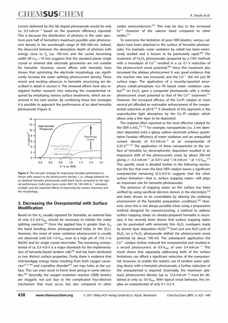
current delivered by this Nb doped photoanode would be onlyca. 0.5 mA cm�2 based on the quantum efficiency reported.This is because the distribution of photons in the solar spec-trum puts half of hematite’s maximum possible solar photocur-rent density in the wavelength range of 500–600 nm. Indeed,the disaccord between the absorption depth of photons withenergy close to Eg (ca. 100 nm) and the carrier harvestingwidth (W+LD = 10 nm) suggests that the standard planar singlecrystal or sintered disk electrode geometries are not suitablefor hematite. However, recent efforts with hematite haveshown that optimizing the electrode morphology can signifi-cantly increase the water splitting photocurrent density. Theserecent and exciting advances in hematite structuring are de-scribed in detail in section 4. The renewed efforts have also in-stigated further research into reducing the overpotential re-quired by employing various surface treatments, which are ex-amined in the next section. By combining these two strategiesit is possible to approach the performance of an ideal hematitephotoanode (Figure 3).
3. Decreasing the Overpotential with SurfaceModification
Based on the Vfb usually reported for hematite, an external biasof only 0.3–0.4 VRHE should be necessary to initiate the watersplitting reaction.[24] Once the applied bias is greater than Vfb,the band bending drives photogenerated holes to the SCLJ.However, the onset of water oxidation photocurrent is usuallynot observed until 0.8–1.0 VRHE even at a high pH of 13.6 (1 m
NaOH) and for single crystal electrodes. The remaining overpo-tential of ca. 0.5–0.6 V is a major drawback for the implementa-tion of hematite-based tandem cells[60] and has been attributedto two distinct surface properties. Firstly there is evidence thatmid-bandgap energy states resulting from both oxygen vacan-cies[25, 31, 64] and crystalline disorder[65] can trap holes at the sur-face. This can even result in Fermi level pining in some electro-des.[66] Secondly, the oxygen evolution reaction (OER) kineticsare sluggish, not just due to the complicated four-electronmechanism that must occur, but also compared to other
oxides semiconductors.[67] This may be due to the increasedFe3+ character of the valence band compared to otheroxides.[31]
To overcome the limitation of poor OER kinetics, various cat-alysts have been attached to the surface of hematite photoan-odes. For example, water oxidation by cobalt has been exten-sively studied and is known to be particularly rapid.[68] Thetreatment of Fe2O3 photoanodes (prepared by a CVD method)with a monolayer of Co2+ resulted in a ca. 0.1 V reduction ofthe photocurrent onset potential.[69] Since this treatment alsoincreased the plateau photocurrent it was good evidence thatthe reaction rate was increased, and the Co2+ did not just fillsurface traps. The application of a recently-reported amor-phous cobalt-phosphate (Co�Pi) based water oxidation cata-lyst[70] on Fe2O3 gave a composite photoanode with a similarphotocurrent onset potential to that of the Co2+ treatment.[71]
However, the increased efficacy of the Co-Pi catalyst at moreneutral pH afforded an noticeable enhancement of the overpo-tential reduction at pH 8.[72] A drawback of this approach is theunproductive light absorption by the Co�Pi catalyst, whichallows only a thin layer to be deposited.
The material often reported as the most effective catalyst forthe OER is IrO2.[73–74] For example, nanoparticles (ca. 2 nm diam-eter) deposited onto a glassy carbon electrode achieve quanti-tative Faradaic efficiency of water oxidation and an unequalledcurrent density of 0.5 mA cm�2 at an overpotential of0.25 V.[75–76] The application of these nanoparticles to the sur-face of hematite by electrophoretic deposition resulted in animpressive shift of the photocurrent onset by about 200 mVgiving J = 0.3 mA cm�2 at 0.9 V and 1.16 mA cm�2 at 1.0 VRHE.[77]
This specific result is detailed further in the following section,but the fact that even the best OER catalyst leaves a significantoverpotential remaining (0.3–0.4 V) suggests that the othersurface limitation—that is, surface trapping states—still playsan important role for hematite photoanodes.
The presence of trapping states on the surface has beenverified by using sacrificial electron donors in the electrolyte,[53]
and been shown to be controllable by altering the oxidizingenvironment of the hematite preparation conditions.[64] How-ever, since this is not always possible when using a preparationmethod designed for nanostructuring, a method to addresssurface trapping states on already-prepared hematite is neces-sary. It has recently been shown that surface trapping statescan be passivated with extremely thin Al2O3 overlayers madeby atomic layer deposition (ALD).[78] Even just one ALD cycle ofAl2O3 on a Fe2O3 photoanode shifted the photocurrent onsetpotential by about 100 mV. The subsequent application theCo2+ catalyst further reduced the overpotential and resulted ina record photocurrent at 0.9 VRHE of over 0.4 mA cm�2. Thisresult shows that separately addressing both of the surfacelimitations can afford a significant reduction of the overpoten-tial, however, to enable the realistic use of tandem water split-ting device with a hematite photoanode, a further reduction ofthe overpotential is required. Essentially, the maximum (pla-teau) photocurrent density (up to 12.6 mA cm�2) must be ob-tained at only ca. 0.6 VRHE. With typical onset behavior, this im-plies an overpotential of only 0.1–0.2 V.
Figure 3. The two-part strategy for improving hematite performance isshown with respect to the photocurrent density, J, vs. voltage behavior foran idealized hematite photoanode (solid black trace) compared to the typi-cal performance (solid grey trace) under AM 1.5G 100 mW cm�2 simulatedsunlight, and the expected effects of improving the surface chemistry andthe morphology.
438 www.chemsuschem.org � 2011 Wiley-VCH Verlag GmbH & Co. KGaA, Weinheim ChemSusChem 2011, 4, 432 – 449
K. Sivula et al.

A different approach, recently reported by Hu et al. holdspromise to reach the high photocurrents at 0.6 VRHE. Here theauthors observed a shift of Vfb in the cathodic direction by150 mV (as measured by the Mott–Schottky technique) using asurface modification with fluoride.[79] Attaining unassistedwater splitting with hematite could even be possible with thistechnique if Vfb could be moved cathodic of 0 VRHE. In a practi-cal device a combination of all three surface treatment strat-egies would be employed to afford the highest photocurrentdensity at the lowest applied potential.
Overall surface treatments have shown great promise in re-ducing the applied potential necessary to onset photocurrentwith hematite photoanodes. However, increasing the solarphotocurrent from the ca. 0.5 mA cm�2 in the single crystalcase towards the maximum possible 12.6 mA cm�2 is more crit-ical for establishing the viability of hematite as a material forsolar energy conversion. Methods to address this challenge arediscussed in the next section.
4. Increasing Photocurrent by MorphologyControl
The small carrier harvesting depth (W+LD) discussed in section2.2 suggests that the ideal morphology of a hematite photoa-node would be one where all of the material is within 10–20 nm of the SCLJ. Of course, one could simply deposit a10 nm layer of hematite on a transparent substrate using a tra-ditional deposition method. The relatively poor absorptivity ofsuch a film could then be overcome by stacking multiplelayers in tandem, assuming the substrate used was a transpar-ent conductor such as fluorine doped tin oxide (FTO). This ap-proach was suggested by Itoh and Bockris in 1984.[59] Whilethis could fundamentally resolve the issue, it is cumbersomeand expensive to implement, and in practice the thin ironoxide films were found to exhibit poor performance due tothe increased recombination of the photogenerated holes.[58]
Fortunately the recent development of tools to control the di-mensions and morphology of materials at the nanometerlength scale has offered more practical solutions for hematite.The application of nanostructuring techniques to PEC solar hy-drogen production has indeed led to advances with many ma-terials. A general overview of this topic is presented by recentreview articles.[80–81] This section will analyze how different dep-osition techniques have allowed the morphology control ofhematite and affected its performance as a photoanode.
4.1 Porous thin films from solution-based colloidal methods
A straightforward way to create nanostructured photoelectro-des is to coat a dispersion of nanoparticles and a porogenonto a conductive substrate. Drying and then heating thesefilms in air burns away the porogen and sinters the remainingoxide, leaving a porous structure of interconnected particles.This concept has been employed effectively with TiO2 for theDSC, and was first attempted with hematite in 1994.[82] In thisseminal work, Fe2O3 sols created by the hydrolysis of FeCl3
were combined with Triton-X100 before they were doctor-
bladed onto FTO and sintered at 560 8C. Micrometer-thick,porous films of necked hematite were observed to have goodadhesion to the substrate and a primary particle size in the25–75 nm range. However the incident photon-to-current effi-ciency (IPCE) of these photoanodes towards water splittingwas quite low—on the order of 1 % at 0.4 VSCE in 0.1 m NaOH(1.4 VRHE) with 400 nm incident irradiation. The IPCE was 100times lower when the anode was illuminated from the hema-tite/electrolyte interface as compared to the substrate/hema-tite interface and the quantum efficiency did not improvewhen LiI was added as a hole scavenger. This led the authorsto conclude that charge carrier recombination was the criticalfactor controlling the photocurrent. The higher quantum effi-ciency of similar particles when dispersed in electrolyte[83]
pointed to grain boundaries in the porous films to be thecause of the excessive recombination and poor performance.This limitation was later addressed by altering the film thick-ness to optimize the light absorption/carrier transport issue.[84]
However, no significant improvement was obtained.Recently the hypothesis that the limitation of these porous
films was the transport and collection of majority carriers wasconfirmed, and relatively high water splitting photocurrentswere obtained after successfully incorporating dopants at suffi-cient concentration.[19] In this work hematite nanoparticles 5–10 nm in diameter, which had been prepared by thermal de-composition of Fe(CO)5 in the gas phase, were dispersed in 2-propanol with acetylacetonate and hydroxypropyl celluloseand coated on FTO or Pt substrates. While no water splittingphotocurrent was observed with these electrodes upon sinter-ing at 400 or 700 8C, 20 min at 800 8C was sufficient to diffuseand activate dopants (Sn4+ or Pt4+ from the substrate) andafford relatively high photocurrents. Under standard illumina-tion conditions (AM 1.5G 100 mW cm�2) 0.56 mA cm�2 at1.23 VRHE and over 1.0 mA cm�2 before the onset of dark cur-rent (1.55 VRHE) were obtained.[19] The same high sintering tem-perature of 800 8C was found to be necessary to afford photo-activity even when (Ti4+) dopant atoms were included in thecolloidal dispersion.[85] This observation suggests that a mini-mum activation energy is required to overcome a barrier forthe diffusion and activation of doping cation impurities in thehematite lattice, and is supported by the report of a drasticchange in the diffusion coefficient of 55Fe3+ isotopes in hema-tite[86] and the further increase in the C3v crystal distortion (seesection 2.1),[87] both of which have been reported to occur atapproximately the same temperature. The latter of these ef-fects was shown to be directly correlated to an increased ab-sorption coefficient in films sintered at these high tempera-tures suggesting that this lattice relaxation is an importantaspect influencing the optoelectronic properties of hematite.[19]
Another effect of the high-temperature treatment is the in-crease of the feature size from the original 5–10 nm to morethan 50 nm via sintering (see Figure 4 c). This large particle sizeprevents the photocurrent densities from surpassing the singlecrystal or sintered disk approaches. To overcome this limitationa method to independently control the feature size and func-tionality with nanostructured oxide electrodes using an encap-sulation approach was recently developed.[88] First, the as-de-
ChemSusChem 2011, 4, 432 – 449 � 2011 Wiley-VCH Verlag GmbH & Co. KGaA, Weinheim www.chemsuschem.org 439
Solar Water Splitting: Progress Using a-Fe2O3 Photoelectrodes

posited films were subjected to a “morphological” annealingto remove the porogen, give good interparticle connections,and set the feature size. Next the films were encapsulated withmesoporous SiO2 using a solution-based precipitation ap-proach. The SiO2 acted as a confinement scaffold during thehigh temperature, “functional” annealing (800 8C) which fol-lowed to diffuse and activate the dopant (Ti4+ included in thedeposition solution). The subsequent removal of the SiO2 bydissolution revealed the functional electrode with a featuresize controlled by the first annealing step. The outcome of ap-plying this approach is shown in Figure 4.
The effect the encapsulation technique had on the nano-structure was immediately evident by eye, when comparingthe resulting electrode to a control heated to 800 8C without aconfinement scaffold. The larger feature size in the controlelectrode resulting from sintering without the SiO2 scatters visi-ble light and the electrode appears translucent with a highopacity. In stark contrast, feature sizes in the confined elec-trode (500 8C morphological annealing) remain too-small toscatter ambient light and the electrode remains transparent
(Figure 4 a). Scanning electron micoscopy images clearly showthe difference of the final feature size, which remains at ca.25 nm with the encapsulation approach and grows to 100–200 nm in the control case (Figure 4 b and c). As the encapsu-lated electrode’s smaller feature size allows the photogenera-tion of holes closer to the SCLJ, a marked increase in the wateroxidizing photocurrent was also observed. The photocurrent ofthe encapsulated electrode reached 1.86 mA cm�2 at 1.43 VRHE
with a maximum photocurrent of 2.34 mA cm�2 before theonset of the dark current while the control electrode gave onlya maximum of 1.5 mA cm�2 (Figure 4 d). This remarkable in-crease of photocurrent was shown to be due an increase ofthe photon conversion efficiency (IPCE) especially in the longerwavelength range.
Despite the demonstrated efficacy of the encapsulationtechnique certain drawbacks prevent it from reaching furtherimprovement of the photocurrent. First, a considerable anodicshift of the photocurrent onset potential was observed (Fig-ure 4 d). This might result from the diffusion a large concentra-tion of Si from the confinement scaffold into the surface ofhematite creating defect states, and could potentially be ad-dressed with a subsequent etching step. Second, the condi-tions found to give a the maximum photocurrent were with a500 8C morphological annealing giving a feature size of ca.25 nm, however attempts to use a lower morphological an-nealing temperature resulted in films with less photocurrentdespite a smaller feature size (which should allow more photo-generated holes to reach the SCLJ). Altering the film thicknesssuggested that a tortuous path for electron conduction withmany grain boundaries limited electron transport in films pre-pared with a morphological annealing temperature less than500 8C. Ultimately, while the solution-based nature of this ap-proach generates much interest in this technique higher pho-tocurrents would be possible if the electron transport limita-tion could be avoided.
4.2 Fe2O3 nanowire arrays
An obvious solution to the problem of majority carrier trans-port in hematite films created from the colloidal approach is touse nanometer-sized rod or wire arrays. An array of single-crys-tal nanorods with diameters in the 10 nm range, attached andoriented orthogonally to a conducting substrate would elimi-nate grain boundaries, and provide a direct path for electroncollection while still allowing photogenerated holes to effi-ciently reach the SCLJ. A simple method to create hematitearrays on a variety of substrates from the controlled precipita-tion of Fe3+ in aqueous solution was first reported by Hagfeldtand co-workers,[89] and investigated for water photoelectrolysissoon after.[27] Bunches of individual 5 nm nanorods with anaverage diameter of 50 nm and a length of 0.1 to 1.5 mm (seeFigure 5, right) were investigated in perpendicular and parallelorientations to the substrate. While the authors were able toshow a small improvement when controlling the orientation(5 % IPCE at 360 nm for the perpendicular nanorods versus 3 %for the parallel) the overall photocurrents remained low underwhite light illumination, even with the hole-scavenging iodide
Figure 4. Electrodes prepared using a solution-based colloidal approachwith an encapsulation technique to control the morphology. The visual ap-pearance (a, top corresponds to the encapsulated sample, bottom corre-sponds to control sample) and scanning electron micrographs of encapsulat-ed (b) and control (c) porous hematite electrodes are shown. The inset in (b)shows the morphology before encapsulation. (d) Electrochemical water oxi-dation photocurrent (solid lines) and dark current (dotted lines) vs. appliedvoltage curves of control (grey) and encapsulated (black) photoanodesunder simulated solar light (AM 1.5G 100 mW cm�2, spectrally corrected) in1 m NaOH electrolyte. Reprinted with permission from [88]. Copyright 2010American Chemical Society.
440 www.chemsuschem.org � 2011 Wiley-VCH Verlag GmbH & Co. KGaA, Weinheim ChemSusChem 2011, 4, 432 – 449
K. Sivula et al.

present. The large difference between the electrode perfor-mance when illuminating from different sides of the semitrans-parent photoanode observed in this work,[67] and a recentreport[90] examining the surface photovoltage on electrodesprepared in the same way, suggests that bulk or surface de-fects are the major factors limiting the performance hematiteprepared by this route. Indeed, aqueous methods of preparinghematite typically pass through a phase containing iron hy-droxide (e.g. , akaganeite, lepidocrocite or goethite) and de-spite the fact that primarily hematite is detected after anneal-ing at 500 8C, it has been shown that at temperatures up to800 8C, a nonstoichiometric composition remains in hematiteprepared by aqueous methods.[91] As such, residual hydroxylgroups or vacancies are likely to blame.
Another facile method to produce hematite nanowires is bythe simple thermal oxidation of iron foils and has been report-ed by many groups.[92–96] Due to the increased volume of theoxide over the metal, when foils of iron are thermally oxidizedunder the right conditions, arrays of Fe2O3 nanowires sponta-neously grow from the surface of the foil. With diameters of20–40 nm and lengths of up to 5 mm (see Figure 5, left) thesenanowire arrays would have large surface area, sufficient lightabsorption and a direct path for the conduction of electrons tothe substrate (since basal planes are oriented perpendicular tothe substrate[95]), making them a very attractive morphologyfor hematite. This simple thermal oxidation method has beendemonstrated on multiple (even transparent) substrates,[96] andmethods for doping the wires have been employed.[92] Howev-er, no convincing reports of activity towards water oxidationhave appeared. This may be due to the defects present innanowires prepared this way or the presence of suboxidesnear the interface of the substrate which greatly enhance re-combination.[97]
Recently, a method to prepare hematite nanorod arraysusing an anodic aluminum oxide (AAO) template was report-ed.[98] Gold was sputtered onto one side of a 60 mm thick AAOmembrane with 200 nm diameter pores. Electrodeposition ofiron oxide from aqueous solution, annealing at 500 8C, and thesubsequent removal of the AAO by dissolution gave the finalstructure. The length of the rods could be varied by changingthe deposition duration. Despite the absence of any intention-al doping, a 10 mm thick rod array showed water oxidationphotocurrent densities of about 1 mA cm�2 at a potential of
1.5 VRHE under AM 1.5 illumination. However, no defined photo-current plateau was observed, suggesting a majority carriertransport limitation in spite of the nanostructure. The incorpo-ration of dopants and annealing at 800 8C may afford higherphotocurrents with this approach. However, based on theknown minority carrier transport properties of hematite thepore size should also be reduced to less than 25 nm to afforda significant increase in photocurrent.
4.3 Electrochemical Fe2O3 nanostructuring
The recent development of nanostructuring techniques usingpotentiostatic anodization has provided another possible routeto create structured hematite photoelectrodes. Prakasam et al.first showed that iron foils could be nanostructured usinganodization in a glycerol-based electrolyte containing 1 %NH4F+1 % HF+0.2 % HNO3.[99] Ordered nanopores were ob-served with pore size ranging from 20 to 250 nm and depthsup to 600 nm depending on the anodization voltage and time.Under simulated solar illumination these photoanodes pro-duced a photocurrent of 0.05 mA cm�2 at 0.4 VSCE in 1 m NaOH(1.45 VRHE). Work by the same group on anodized Ti�Fe�Oelectrodes is notable here due to the high photocurrent densi-ties reported (1.1 mA cm�2 at 1.4 VRHE in 1 m NaOH) despite thepresence of both hematite and rutile in the photoanode pre-pared at the optimized conditions.[100] In contrast, very well de-fined nanotube arrays of pure iron oxide created from ironfoils have been subsequently reported by a different researchgroup.[101] In this work, a single anodization step with 0.1 m
NH4F+3 vol % water in ethylene glycol created nanotubes withwalls less than 50 nm and lengths of about 1.5 mm. After anoptimized annealing treatment these electrodes were found tobe a mixture of both hematite and maghemite by XRD andhad only small photocurrents (160 mA cm�2, 1.23 VRHE underAM 1.5 illumination compared to 120 mA cm�2 dark current).However, a double step anodization procedure with the addi-tion of sodium tripolyphosphate in the electrolyte, and thesubsequent annealing created a dendrite-like morphology situ-ated over the tube array. Electrodes prepared this way exhibit-ed a photocurrent of about 1 mA cm�2 under AM 1.5 illumina-tion and at 1.23 VRHE. A large carrier concentration (1021 cm�3)was found via Mott–Schottky indicating a large amount ofdopant or impurity present. The authors attribute the highphotocurrent to the double layered structure which includesboth a large surface area for water oxidation and a verticallyorientated nanotube array for electron transport.
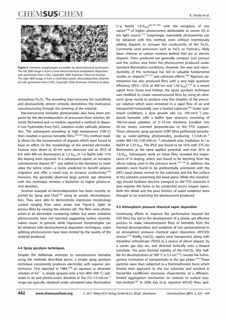
In subsequent work by the same group, a sono-electro-chemical anodization method was employed to obtain eithernanoporous or nanotubular Fe2O3, depending on the anodiza-tion conditions.[102] The optimization of conditions gave nano-tubes with walls an impressive 5–6 nm thick and micrometersin length (see Figure 6, left). Annealing these films resulted inpure hematite which gave similar photocurrents (ca.1 mA cm�2 at AM 1.5 and 1.23 VRHE) and similar carrier densitiesto the previous work. While the initial tube size presented inthis work is remarkable and an important step for obtaininghematite with the ideal morphology, the tubes were initially
Figure 5. Examples of hematite nanowire morphologies: SEM images ofhematite prepared by the thermal oxidation method (left image, reprintedwith permission from [92], copyright 2005 American Institute of Physics) andaqueous method (right image, reprinted with permission from [89], copy-right 2001 American Chemical Society).
ChemSusChem 2011, 4, 432 – 449 � 2011 Wiley-VCH Verlag GmbH & Co. KGaA, Weinheim www.chemsuschem.org 441
Solar Water Splitting: Progress Using a-Fe2O3 Photoelectrodes
amorphous Fe2O3. The annealing step necessary for crystallinityand photoactivity almost certainly demolishes the meticulousnanostructuring through the sintering of the material.
Nanostructured hematite photoanodes also have been pre-pared by the electrodeposition of precursors from solution. Re-cently McFarland and co-workers reported a method to depos-it iron hydroxides from FeCl3 solutions under cathodic polariza-tion. The subsequent annealing at high temperature (700 8C)then resulted in porous hematite films.[28, 104] This method readi-ly allows for the incorporation of dopants which were found tohave an effect on the morphology of the sintered electrodes.Feature sizes down to 40 nm were observed and an IPCE of8 % with 400 nm illumination at 1.2 VRHE in 1 m NaOH with 15 %Mo doping were reported. In a subsequent report, an isovalentsubstitutional dopant Al3+ was added to the hematite to mod-ulate the lattice strain—a factor predicted to benefit polaronmigration and offer a novel way to increase conductivity.[105]
However, the generally observed large particle size obtainedwith this technique remains a limitation to higher photocur-rent densities.
Another example of electrodeposition has been recently re-ported by Spray and Choi[103] using an anodic electrodeposi-tion. They were able to demonstrate impressive morphologycontrol ranging from wires arrays (see Figure 6, right) toporous films by varying the solution pH. The films were photo-active in an electrolyte containing iodide, but water oxidationphotocurrents were not reported suggesting surface recombi-nation issues. In general, while impressive morphologies canbe obtained with electrochemical deposition techniques, watersplitting photocurrents have been limited by the quality of thematerial produced.
4.4 Spray pyrolysis techniques
Despite the deliberate attempts to nanostructure hematiteusing the methods described above, a simple spray pyrolysistechnique consistently produces electrodes with superior per-formance. First reported in 1984,[106] an aqueous or ethanolicsolution of Fe3+ is simply sprayed onto a hot (400–500 8C) sub-strate in air and photocurrent densities in the 0.5–1.0 mA cm�2
range are typically obtained under simulated solar illumination
(1 m NaOH, 1.6 VRHE)[66, 107–109] with the exception of onereport[110] of higher photocurrent attributable to excess UV inthe light source.[111] Surprisingly, reasonable photoactivity canbe obtained with this method, even without intentionallyadding dopants to increase the conductivity of the Fe2O3.Commonly used precursors such as FeCl3 or Fe(AcAc)3 likelyleave chlorine or carbon residues behind that act as electricdopants. Films produced are generally compact (not porous)and the surface area limits the photocurrent produced understandard illumination conditions. However, the ease and repro-ducibility of this technique has led to valuable fundamentalstudies on dopants[107, 112] and substrate effects.[108] Rigorous op-timization has also produced films with a very high quantumefficiency (IPCE = 25 % at 400 nm and 1.42 VRHE).[112] In a recentreport from Duret and Gr�tzel, the spray pyrolysis techniquewas modified to create nanostructured films by using an ultra-sonic spray nozzle to produce very fine droplets of the precur-sor solution which were entrained in a rapid flow of air andtransported horizontally over a heated substrate.[66] Under opti-mized conditions, a slow growth rate (ca. 100 nm h�1) pro-duced hematite with a leaflet type structure consisting of100 nm-sized platelets of 5–10 nm thickness bundled into50 nm sheets oriented perpendicular to the FTO support.These ultrasonic spray pyrolysis (USP) films performed remarka-bly as water-splitting photoanodes, producing 1.3 mA cm�2
under AM 1.5G (100 mW cm�2) simulated solar irradiation in 1 m
NaOH at 1.23 VRHE. The IPCE was found to be 16 % with 375 nmillumination at the same applied potential, and over 30 % at1.6 VRHE. Subsequent work on these films revealed the impor-tance of Si doping, which was found to be leeching from thesilicon tubing used in the previous work.[113–114] In addition, theplatelets were found to be preferentially orientated with the(001) basal planes normal to the substrate and the flat surfaceof the platelets presenting the basal plane. While this morphol-ogy should facilitate electron transport to the FTO substrate italso requires the holes to be conducted across oxygen layers.Both this detail and the poor kinetics of water oxidation werethought to be restricting the photocurrent produced.
4.5 Atmospheric pressure chemical vapor deposition
Continuing efforts to improve the performance beyond theUSP films has led to the development of a simple, yet effectiveprocess to make nanostructured films of hematite from thethermal decomposition and oxidation of iron pentacarbonyl inan atmospheric pressure chemical vapor deposition (APCVD)reactor.[113] Briefly, Fe(CO)5 vapors were transported, along withtetraethyl orthosilicate (TEOS) as a source of silicon dopant, bya carrier gas (dry air), and directed vertically onto a heatedsubstrate. The poor thermal stability of the Fe(CO)5 (the half-life for decomposition at 300 8C is 5.3 ms[115]) caused the homo-genous nucleation of nanoparticles in the gas phase.[116] Theseparticles were then subjected to a thermophoretic force whichlimited their approach to the hot substrate and resulted infractal-like cauliflower structures characteristic of a diffusion-limited aggregation mechanism (in contrast to surface reac-tion-limited).[65] In 2006 Kay et al. reported APCVD films opti-
Figure 6. Hematite morphologies accessible by electrochemical techniques:The left SEM image is from a sono-electrochemical anodization (Reprintedwith permission from [102], Copyright 2009 American Chemical Society).The right SEM image is from a controlled anodic electrodeposition (Reprint-ed with permission from [103] , Copyright 2009 American Chemical Society).
442 www.chemsuschem.org � 2011 Wiley-VCH Verlag GmbH & Co. KGaA, Weinheim ChemSusChem 2011, 4, 432 – 449
K. Sivula et al.

mized with a substrate temperature of 420 8C and using a carri-er gas flow rate of 2 L min�1. Cauliflower-type structures with aminimum feature size of 5–10 nm grew on FTO substrates atrate of about 100 nm min�1. The best film produced a photo-current density of 1.8 mA cm�2 at 1.23 VRHE under standard illu-mination in 1 m NaOH and was further increased to2.2 mA cm�2 by treating the surface with Co2+ ions. Similar tothe films prepared by the USP method, the silicon dopant wasfound to affect the nanostructure, producing a smaller featuresize in both cases and an alignment of the basal crystal planenormal to the substrate.[69, 113]
In continuing work with this deposition technique ferroceneand tetramethyl orthosilicate (TMOS) were found to be viablesources of iron and silicon, respectively.[117–118] The use of ferro-cene is notable for replacing the toxic iron pentacarbonyl,however the photocurrent density obtained remained lessthan 1 mA cm�2. With the standard Fe(CO)5/TEOS system Cesaret al. showed a large temperature effect on the nanostructurewhich corresponded to the performance of the electrodes.[65]
Higher temperatures were found to decrease the depositionrate, lead to a larger particle size, and reduced the photocur-rent density. A Mott–Schottky analysis gave the calculateddonor density, Nd, of the Si doped Fe2O3 films as 1.7 �1020 cm�3—close to the predicted 6 � 1020 cm�3 if the knownincorporation of silicon (1.6 at % Si)[69] was substitutionally in-corporated into the lattice as Si4+. Based on classic depletionlayer theory,[61] this led the authors to suggested that a space-charge layer of ca. 5 nm could still be present and aiding holetransport the SCLJ even in the small features on the top of theAPCVD film. In addition, changing the deposition time definedan optimum thickness (500 nm) for photocurrent productionfrom front side illumination (i.e. , upon the hematite/electrolyteinterface). A slow decrease in photocurrent was observed forthicker films resulting in less than 1 mA cm�2 for 1 mm thickfilms. This implied an electron transport limitation, which wassubsequently addressed by tuning the particle to precursorratio.
An important parameter governing the structure and qualityof nanostructured prepared by particle-assisted CVD systems,like the APCVD of Fe(CO)5, is the particle to precursor ratio.[119]
By changing the carrier gas flow rate, keeping the same con-centration of iron precursor, and re-optimizing the other exper-imental parameters, the amount of time the precursors residedin the critical region of particle nucleation and growth abovethe deposition substrate was effectively tuned. It was foundthat using a carrier gas flow rate three times higher than theprevious result (6 L min�1) enhanced the preferential orienta-tion of the basal planes normal to the substrate (enhancingmajority carrier transport), but did not change the primary par-ticle size.[120] This resulted in an optimized thickness of 800 nm,and photocurrents above 3 mA cm�2 (see Figure 7). To improveupon the overpotential reduction found with the Co2+ treat-ment, the IrO2 nanoparticle OER catalyst was then depositedonto the Fe2O3 cauliflowers by an eletrophoretic process. Thisproduced a 200 mV shift in the photocurrent onset potentialand photocurrent of 3.3 mA cm�2 at 1.23 VRHE under standardtesting conditions.[77]
The photocurrent produced was further verified by measur-ing the photoanode IPCE at 1.23 VRHE. Over 50 % of the pho-tons with l = 300 nm, 39 % at 400 nm, and a remarkable 20 %at 500 nm were effectively harvested using this nanostructure.Moreover, the integration of the product of the IPCE and thestandard AM 1.5G solar photon flux over the entire wavelengthrange gave a photocurrent of 3.01 mA cm�2, verifying the lightsource used for the J–V measurements. The photocurrent wasfound to be stable for many scans, however under extendedmeasurement the IrO2 nanoparticles detached from the surfaceand the photocurrent onset potential shifted back to the origi-nal value. Despite this limitation, which could possibly over-come using an appropriate linking strategy, this result clearlydemonstrated that water oxidizing photocurrents over3 mA cm�2 at relatively low bias potentials are possible withhematite using the combined strategy of morphology controland surface modification. This demonstration also thrusts theperformance of hematite past the other oxides studied for PECwater oxidation to be the most efficient at converting solarlight into energy stored in a tandem cell. If the bias requiredwas applied by two PV cells in tandem each delivering 0.6 V
Figure 7. Characterization of Si-doped Fe2O3 electrodes prepared by theAPCVD technique. a, b) Cross-sectional morphologies of optimized electro-des prepared with carrier gas flow rates of 2 and 6 L min�1, respectively. c) J–V curves of an unmodified hematite photoanode prepared at 6 L min�1
(solid trace) and the same anode after functionalization with IrO2 nanoparti-cles (dashed–dotted trace) in 1 m NaOH solution (pH 13.6). The dashed traceis the photocurrent for an electrode prepared at 2 L min�1. Photocurrentscorrespond to AM 1.5 G 100 mW cm�2 simulated sunlight. d) The incidentphoton conversion efficiency (IPCE) at an applied potential of +1.23 VRHE (cir-cles) and the AM 1.5 G 100 mW cm�2 solar spectrum (black trace) are multi-plied together to give the number of photons stored in the form of hydro-gen (shaded area). The dashed trace is the integrated photocurrent andreaches 3.01 mA cm�2. Reprinted from [77]. Copyright 2010 John Wiley andSons.
ChemSusChem 2011, 4, 432 – 449 � 2011 Wiley-VCH Verlag GmbH & Co. KGaA, Weinheim www.chemsuschem.org 443
Solar Water Splitting: Progress Using a-Fe2O3 Photoelectrodes

and 6.6 mA cm�2, a total solar to hydrogen efficiency of 4.8 %would be obtained.
While this is a considerable step towards high performancehematite, the photocurrent density remains far from the12.6 mA cm�2 possible. This is because, despite absorbingalmost all of the light (with hn>Eg) the quantum conversionefficiencies are still relatively low for wavelengths near theband edge (500<l<600) where, half of hematite’s possiblesolar photocurrent is available. This can be primarily attributedto the cauliflower-type morphology, which has an appropriatefeature size of 10 nm at the SCLJ, but the individual cauliflowerstructures consist of thick stems which increase the number ofphotons absorbed far from the SCLJ.
4.6 Extremely thin absorber approach
The techniques discussed until now attempt to increase thephotocurrent by nanostructuring the hematite itself. However,another strategy that can place all of the hematite in proximityto the SCLJ and include sufficient material for light absorptionis to coat an extremely thin layer on a high-surface area, nano-structured scaffold in analogy to the DSC[121] and extremelythin absorber (ETA) PVs.[122]
This concept was recently demonstrated using a nanostruc-tured WO3 as the host scaffold.[123] In this work the scaffoldwas coated with a thin layer (ca. 60 nm) of Fe2O3 by theAPCVD method and a 20 % increase in the photocurrent wasobserved over control samples prepared on flat FTO sub-strates. This enhancement was attributed to an increase in theabsorbed photon to current efficiency (APCE), especially in thewavelength range from 500 to 600 nm. However, the thick-ness-optimized 60 nm layer of hematite was too thick basedon the known hole transport limitations. Attempts to use thin-ner films of iron oxide resulted in poor performance, similar toother reports of thin films Fe2O3,[58] and pointed to a high re-combination of photogenerated holes at the hematite/scaffoldinterface.
This limitation has recentlybeen addressed by including aSnO2
[108] or a SiOx[124] buffer layer
the problematic interface. Forthe latter report, a simple spaydeposition was used to makehighly uniform compact films ofFe2O3 on FTO substrates to firstexamine the effect of the thick-ness on the interfacial recombi-nation. A minimum thickness of22 nm was required to observeappreciable photoanode behav-ior. However when a SiOx bufferlayer was deposited on the FTO,reasonable photocurrents wereobtained with only a 12.5 nmthickness of Fe2O3. In addition,comparing films of similar thick-ness with and without the
buffer layer showed less recombination upon examining pho-tocurrent transient behavior. Moreover, it was found that thebuffer layer significantly altered the film nucleation andgrowth characteristics, and consequently the crystallinity. Un-fortunately, the best ultrathin hematite films with employedbuffer layer showed slightly lower values for the APCE com-pared to the state-of-the-art APCVD films. This is possibly dueto the high reflectivity of the compact and flat films. In gener-al, the ETA/buffer layer/scaffold approach provides a clear pathto overcoming all of hematite’s limitations by decoupling thelight absorption and the charge transport. Research usinghematite with this approach is relatively new and further inves-tigations into buffer layers and appropriately structured scaf-folds should ultimately produce photocurrents higher thanFe2O3 prepared by the APCVD technique.
4.7 Nanostructuring method comparison
Several different approaches have been taken to nanostructureFe2O3 for use in photoelectrochemical water splitting, and atleast as many methods of characterizing the electrodes havealso appeared. As such it can be difficult to compare the re-sults in the literature, especially when variations in light sour-ces give large overestimations of photocurrents due to super-fluous UV light. A recent review addresses these issues andoutlines standardized techniques for assessing photoelectro-des.[125] While not all of the reports discussed in this sectionhave followed these suggestions it can still be helpful to com-pare the major accomplishments from the different structuringtechniques and the resulting performance. This is done inTable 1.
Overall, it is clear there is a strong dependence of the perfor-mance of synthetic hematite on the deposition technique. In-terestingly, while methods such as spray pyrolysis and CVDconsistently produce electrodes photoactive for water oxida-tion at low temperatures (400–500 8C), solution-based methods
Table 1. Comparison of hematite photoanode structuring methods
Technique Feature size Do-pant
Performance
Single crystal[57] micrometer Nb IPCE 37 % at 370 nm and 1.23 VRHE
Sintered polycrystalline disk[47] micrometer Si IPCE 34 % at 400 nm and 1.23 VRHE
Colloidal deposition ofporous films[88]
25 nm Ti 2.34 mA cm�2 at 1.63 VRHE and AM 1.5 (100 mW cm�2)andIPCE 40 % at 400 nm and 1.6 VRHE
Solution-based nanowires[27] 50 nm � 500 nm none IPCE 7 % at 400 nm and 0.9 VRHE (in KI)Potentiostatic anodization(nanotubes)[102]
6 nm � 1 mm none Before annealing: None reportedAfter annealing:[a] 1.0 mA cm�2 at 1.23 VRHE andAM 1.5 (87 mW cm�2)
Electro-deposition[28] 20–50 nm Mo IPCE 8 % at 400 nm and 1.2 VRHE
Ultrasonic spray pyrolysis[66, 114] 10 nm � 300 nm Si 1.5 mA cm�2 at 1.23 VRHE and AM 1.5 (100 mW cm�2)and IPCE 14 % at 400 nm and 1.23 VRHE
Atmospheric pressure CVD[77] 5 nm � 800 nm Si 3.3 mA cm�2 at 1.23 VRHE and AM 1.5 (100 mW cm�2)and IPCE 39 % at 400 nm (50 % at 325 nmand 16 % at 550 nm) and 1.23 VRHE
Extremely thin absorber[123] 50 nm film Si 1.3 mA cm�2 at 1.23 VRHE and AM 1.5 (100 mW cm�2)and IPCE 26 % at 400 nm and 1.43 VRHE
[a] Feature size not reported after annealing.
444 www.chemsuschem.org � 2011 Wiley-VCH Verlag GmbH & Co. KGaA, Weinheim ChemSusChem 2011, 4, 432 – 449
K. Sivula et al.

such as the colloidal and electrodeposition approaches requiremuch higher temperatures (700–800 8C) to produce photoac-tive hematite. This is certainly related to the quality of the pre-pared material in terms of crystallinity, impurity concentrations,and dopant incorporation, and a further understanding of thisaspect is important to pursue.
Also worth noting is that the IPCE values at ca. 400 nmrarely exceed that of the single crystal or sintered polycrystal-line electrodes prepared during the first decade of work. Thechampion electrodes made by APCVD show only a modest in-crease in the conversion efficiency with 400 nm photons. Theexplanation for the significant increase in photocurrent ob-served with the APCVD and the colloidal solution-depositedelectrodes has, of course, been the nanostructuring, that hasallowed increases conversion of the longer wavelengths oflight. Further work on the nanostructuring will, no doubt, seesolar photocurrents rise, but the increase in IPCE beyond 40 %at 400 nm and 1.23 VRHE will require further research directedat increasing the understanding of hematite photoanodes.
5. Advanced Understanding by using Electro-chemical Impedance Spectroscopy
Many electrochemical techniques have been used to character-ize hematite photoanodes with the goal of understanding itsperformance and limitations. The most often employed— elec-trochemical impedance spectroscopy (EIS)—has proven to bevaluable for ideal systems like single crystals. However, themany different preparation techniques and the advent ofnanostructured electrodes have complicated efforts to under-stand and compare results obtained from EIS. Fortunately,recent efforts have provided significant advances in applyingthis classic technique to increase the understanding of hema-tite photoelectrodes. In this section the latest developmentscharacterizing hematite photoanodes with EIS are discussed.
As a modulation technique, EIS consists of applying a time-dependant signal to the electrode, usually a sinusoidal pertur-bation of bias potential, and measuring the complex responseof the electrode. By varying the excitation frequency, processeswith different time constants can be resolved. The further anal-ysis of the frequency-dependant response using an electronicmodel can separate the different aspects of charge transport,charge trapping, and charge transfer at the interface with elec-trolyte. During an EIS experiment the electrode dark- or photo-current density is typically recorded while applying an alternat-ing current (AC) signal with frequency, f (0.1 Hz< f<106 Hz),superimposed on the bias potential. A major advantage of EISover other spectroscopic techniques is that it allows samplecharacterization under working conditions (in electrolyte underbias potential). The application of the well-known Mott–Schott-ky (MS) relation allows the extraction of Vfb and Nd by plottingthe inverse square of the capacitance versus the applied bias.Typically, the capacitance is determined by fitting the frequen-cy responses with a simple resistor–capacitor (RC) circuitmodel (see Figure 8 a). A single frequency,[30, 50, 56] multiple fre-quencies,[105] extrapolating to an infinite frequency,[54, 57, 126] oran entire range of high frequencies[65, 127–128] have been used to
fit the circuit model. Consistent values of Vfb from 0.4–0.6 VRHE
and Nd on the order of 1017 cm�3 (for undoped) to 1021 cm�3
(for heavily doped samples) have been reported for bothplanar and structured electrodes.[24, 127–128]
However since the classic MS relation relies on a simple par-allel-plate capacitor model the application of EIS data from realsystems has often been problematic. For example, frequencydispersion in MS plots is often observed low frequencies. Thishas been attributed to non-idealities such as roughness of thesamples, relaxation of the dielectric constant in the spacecharge region, and surface trapping states,[129] and explains thepreferential use of high frequency to determine the sample ca-pacitance. In addition, MS plots of hematite photoanodes haveexhibited large deviations from linearity when Vb @ Vfb. Thisphenomenon has been attributed to deep energetic levels par-tially ionized in the space charge region (Goodman model).[130]
To account for this, the observed EIS response was fitted witha more sophisticated circuit model taking in to account theseintrabandgap states (Figure 8 b). Using this model, these stateswere found to lie 0.5–0.6 eV below the conductionband[30, 54, 131] and associated with a trapping time constantabout 0.4 ms. Some studies also established the presence ofshallow donors, or trap states located at 0.1–0.2 eV under theconduction band using this model at low bias potential. Never-theless McAlpine and Fredlein[132] observed severe limitationsto this model and more recent studies using nanostructuredhematite have not reported similar behavior, possibly due tosmall features exhibiting low bulk-to-surface ratio. For nano-structures, a superlinear trend of the MS plot has also been ob-served. This has recently been explained in a terms of decreasein the surface area contributing to the capacitance.[65] As thehematite photoanode is biased in the anodic direction, the
Figure 8. a–c) Common electronic models describing iron oxide behavior inEIS spectroscopy: model (a) represents a simple RC circuit (Helmholtz capaci-tance, CH, constant) used to calculate the flat band potential and the donordensity from Mott-Schottky equation, applicable at high frequency. Model(b) represents the electronic circuit that takes in account trap states (i.e. sur-face states at low bias potential, bulk states far from the flat band). Model(c) accounts for a non-negligible Helmholtz capacitance due to the presenceof a high surface area (nanostructure) or surface states. d) Typical responseof a hematite electrode (prepared by APCVD[69]) to electrochemical impe-dance spectroscopy (presented by a Nyquist plot) scanning the frequencyfrom 1 MHz to 0.05 Hz at different applied bias potentials. At high frequen-cy (small impedance), only one semicircle is distinguishable whereas at lowfrequency (large impedance) a second semicircle appears. Often the two aredifficult to distinguish (e.g. , at 0.8 VRHE).
ChemSusChem 2011, 4, 432 – 449 � 2011 Wiley-VCH Verlag GmbH & Co. KGaA, Weinheim www.chemsuschem.org 445
Solar Water Splitting: Progress Using a-Fe2O3 Photoelectrodes
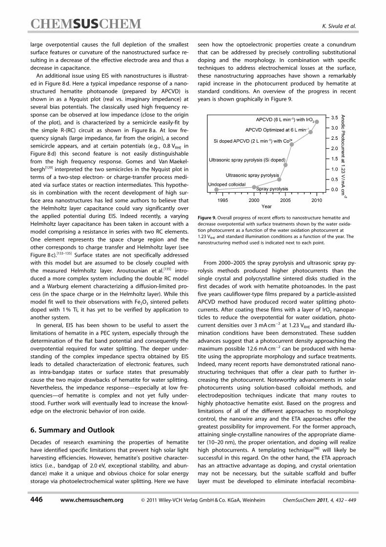
large overpotential causes the full depletion of the smallestsurface features or curvature of the nanostructured surface re-sulting in a decrease of the effective electrode area and thus adecrease in capacitance.
An additional issue using EIS with nanostructures is illustrat-ed in Figure 8 d. Here a typical impedance response of a nano-structured hematite photoanode (prepared by APCVD) isshown in as a Nyquist plot (real vs. imaginary impedance) atseveral bias potentials. The classically used high frequency re-sponse can be observed at low impedance (close to the originof the plot), and is characterized by a semicircle easily-fit bythe simple R-(RC) circuit as shown in Figure 8 a. At low fre-quency signals (large impedance, far from the origin), a secondsemicircle appears, and at certain potentials (e.g. , 0.8 VRHE inFigure 8 d) this second feature is not easily distinguishablefrom the high frequency response. Gomes and Van Maekel-bergh[129] interpreted the two semicircles in the Nyquist plot interms of a two-step electron- or charge-transfer process medi-ated via surface states or reaction intermediates. This hypothe-sis in combination with the recent development of high sur-face area nanostructures has led some authors to believe thatthe Helmholtz layer capacitance could vary significantly overthe applied potential during EIS. Indeed recently, a varyingHelmholtz layer capacitance has been taken in account with amodel comprising a resistance in series with two RC elements.One element represents the space charge region and theother corresponds to charge transfer and Helmholtz layer (seeFigure 8 c).[133–135] Surface states are not specifically addressedwith this model but are assumed to be closely coupled withthe measured Helmholtz layer. Aroutounian et al.[135] intro-duced a more complex system including the double RC modeland a Warburg element characterizing a diffusion-limited pro-cess (in the space charge or in the Helmholtz layer). While thismodel fit well to their observations with Fe2O3 sintered pelletsdoped with 1 % Ti, it has yet to be verified by application toanother system.
In general, EIS has been shown to be useful to assert thelimitations of hematite in a PEC system, especially through thedetermination of the flat band potential and consequently theoverpotential required for water splitting. The deeper under-standing of the complex impedance spectra obtained by EISleads to detailed characterization of electronic features, suchas intra-bandgap states or surface states that presumablycause the two major drawbacks of hematite for water splitting.Nevertheless, the impedance response—especially at low fre-quencies—of hematite is complex and not yet fully under-stood. Further work will eventually lead to increase the knowl-edge on the electronic behavior of iron oxide.
6. Summary and Outlook
Decades of research examining the properties of hematitehave identified specific limitations that prevent high solar lightharvesting efficiencies. However, hematite’s positive character-istics (i.e. , bandgap of 2.0 eV, exceptional stability, and abun-dance) make it a unique and obvious choice for solar energystorage via photoelectrochemical water splitting. Here we have
seen how the optoelectronic properties create a conundrumthat can be addressed by precisely controlling substitutionaldoping and the morphology. In combination with specifictechniques to address electrochemical losses at the surface,these nanostructuring approaches have shown a remarkablyrapid increase in the photocurrent produced by hematite atstandard conditions. An overview of the progress in recentyears is shown graphically in Figure 9.
From 2000–2005 the spray pyrolysis and ultrasonic spray py-rolysis methods produced higher photocurrents than thesingle crystal and polycrystalline sintered disks studied in thefirst decades of work with hematite photoanodes. In the pastfive years cauliflower-type films prepared by a particle-assistedAPCVD method have produced record water splitting photo-currents. After coating these films with a layer of IrO2 nanopar-ticles to reduce the overpotential for water oxidation, photo-current densities over 3 mA cm�2 at 1.23 VRHE and standard illu-mination conditions have been demonstrated. These suddenadvances suggest that a photocurrent density approaching themaximum possible 12.6 mA cm�2 can be produced with hema-tite using the appropriate morphology and surface treatments.Indeed, many recent reports have demonstrated rational nano-structuring techniques that offer a clear path to further in-creasing the photocurrent. Noteworthy advancements in solarphotocurrents using solution-based colloidal methods, andelectrodeposition techniques indicate that many routes tohighly photoactive hematite exist. Based on the progress andlimitations of all of the different approaches to morphologycontrol, the nanowire array and the ETA approaches offer thegreatest possibility for improvement. For the former approach,attaining single-crystalline nanowires of the appropriate diame-ter (10–20 nm), the proper orientation, and doping will realizehigh photocurrents. A templating technique[98] will likely besuccessful in this regard. On the other hand, the ETA approachhas an attractive advantage as doping, and crystal orientationmay not be necessary, but the suitable scaffold and bufferlayer must be developed to eliminate interfacial recombina-
Figure 9. Overall progress of recent efforts to nanostructure hematite anddecrease overpotential with surface treatments shown by the water oxida-tion photocurrent as a function of the water oxidation photocurrent at1.23 VRHE and standard illumination conditions as a function of the year. Thenanostructuring method used is indicated next to each point.
446 www.chemsuschem.org � 2011 Wiley-VCH Verlag GmbH & Co. KGaA, Weinheim ChemSusChem 2011, 4, 432 – 449
K. Sivula et al.
tion. Parallel with developing these approaches to morphologycontrol, more work needs to be done to further understandhematite’s intrinsic limitations. For example, the sub-50 %quantum efficiencies (even at short wavelengths in optimizedsingle crystal photoanodes), the ultrafast carrier recombination,and the interband-gap states found in hematite suggest pho-tocurrents approaching 12.6 mA cm�2 will be difficult, if not im-possible, to achieve given our lack of understanding. However,recent combinatorial efforts to optimize both the alloy compo-sition[10, 136] and doping in hematite[137] may indicate new ave-nues for investigation. In addition, a significant reduction ofthe overpotential for water oxidation is urgently required. Incomparison to the extensive work done on TiO2,[138] relativelylittle is known about the surface chemistry of hematite. Onlyrecently have some important and interesting reactivity differ-ences on hematite surfaces have been observed,[139–140] and fur-ther work on this topic is necessary.
Finally, in many ways the development of Fe2O3 reportedhere can be considered analogous to the development of sili-con photovoltaics. At the time of the beginning of the terres-trial photovoltaic industry in the 1970s, the conventionalwisdom was that crystalline silicon solar cells were hopelesslyexpensive and too inefficient to be a viable energy source.[141]
However the fact that silicon possessed ideal properties for aphotovoltaic device could not be ignored, and today siliconsolar cells are the dominate form of photovoltaic energy con-version thanks to the extensive technological effort put into itsdevelopment. Hematite similarly possesses many ideal charac-teristics for solar water splitting. The recent developments pre-sented here give strong prospect that continued efforts willbring photoanodes with performances sufficient for commer-cial application.
7. Symbols and Abbreviations
a Absorption coefficientAC Alternating currentALD Atomic layer depositionAPCVD Atmospheric pressure CVDCVD Chemical vapor depositionDSC Dye-sensitized solar cellEg Bandgap energyEIS Electrochemical impedance spectroscopyFTO Fluorine-doped tin oxideJ Current densityLD Diffusion length
MS Mott–SchottkyNd Donor densityOER Oxygen evolution reactionPC PhotocatalyticPEC PhotoelectrochemicalPV PhotovoltaicRC Resistor-capacitorRHE Reversible hydrogen electrodeSCE Saturated calomel electrodeSCLJ Semiconductor/liquid junctionSTH Solar-to-hydrogen conversion efficiency
Vb Applied bias potentialVfb Flat-band potentialVRHE Volts vs. RHEVSCE Volts vs. SCEW Depletion layer width
Acknowledgements
The frontispiece photograph of the Valley of Fire State Park(Nevada, USA) was graciously provided by Frank Kovalchek.
Keywords: catalysis · energy conversion · metal oxides ·nanostructures · water splitting
[1] M. Gr�tzel, Nature 2001, 414, 338 – 344.[2] D. Pimentel, A. Marklein, M. A. Toth, M. Karpoff, G. S. Paul, R. McCor-
mack, J. Kyriazis, T. Krueger, Energies (Basel, Switz.) 2008, 1, 41 – 78.[3] J. Turner, G. Sverdrup, M. K. Mann, P. C. Maness, B. Kroposki, M. Ghirar-
di, R. J. Evans, D. Blake, Int. J. Energy Res. 2008, 32, 379 – 407.[4] M. D. Hern�ndez-Alonso, F. Fresno, S. Suarez, J. M. Coronado, Energy
Environ. Sci. 2009, 2, 1231 – 1257.[5] K. Maeda, K. Domen, J. Phys. Chem. Lett. 2010, 1, 2655 – 2661.[6] A. J. Esswein, D. G. Nocera, Chem. Rev. 2007, 107, 4022 – 4047.[7] P. J. Boddy, J. Electrochem. Soc. 1968, 115, 199.[8] A. Fujishima, K. Honda, Nature 1972, 238, 37.[9] M. Szklarczyk, J. O. Bockris, J. Phys. Chem. 1984, 88, 5241 – 5245.
[10] M. Woodhouse, B. A. Parkinson, Chem. Soc. , Rev. 2009, 38, 197 – 210.[11] A. Walsh, S. H. Wei, Y. Yan, M. M. Al-Jassim, J. A. Turner, Phys. Rev. B
2007, 76, 165119.[12] J. Greeley, T. F. Jaramillo, J. Bonde, I. B. Chorkendorff, J. K. Norskov, Nat.
Mater. 2006, 5, 909 – 913.[13] L. J. Minggu, W. R. W. Daud, M. B. Kassim, Int. J. Hydrogen Energy 2010,
35, 5233 – 5244.[14] O. Khaselev, J. A. Turner, Science 1998, 280, 425 – 427.[15] M. Ni, M. K. H. Leung, D. Y. C. Leung, K. Sumathy, Renewable Sustainable
Energy Rev. 2007, 11, 401 – 425.[16] C. Santato, M. Ulmann, J. Augustynski, J. Phys. Chem. B 2001, 105,
936 – 940.[17] A. B. Murphy, P. R. F. Barnes, L. K. Randeniya, I. C. Plumb, I. E. Grey, M. D.
Horne, J. A. Glasscock, Int. J. Hydrogen Energy 2006, 31, 1999 – 2017.[18] R. M. Cornell, U. Schwertmann, The Iron Oxides : Structure, Properties,
Reactions, Occurrences, and Uses, 2nd Ed., Wiley-VCH, Weinheim, 2003.[19] K. Sivula, R. Zboril, F. Le Formal, R. Robert, A. Weidenkaff, J. Tucek, J.
Frydrych, M. Gratzel, J. Am. Chem. Soc. 2010, 132, 7436 – 7444.[20] R. Zboril, M. Mashlan, D. Petridis, Chem. Mater. 2002, 14, 969 – 982.[21] N. Iordanova, M. Dupuis, K. M. Rosso, J. Chem. Phys. 2005, 122, 144305.[22] A. I. Galuza, A. B. Beznosov, V. V. Eremenko, Low Temp. Phys. 1998, 24,
726 – 729.[23] L. A. Marusak, R. Messier, W. B. White, J. Phys. Chem. Solids 1980, 41,
981 – 984.[24] T. Lindgren, L. Vayssieres, H. Wang, S. E. Lindquist, Chem. Phys. Nano-
struct. Semicond. 2003, 83 – 110.[25] R. F. G. Gardner, D. W. Tanner, F. Sweett, J. Phys. Chem. Solids 1963, 24,
1183.[26] J. H. Kennedy, K. W. Frese, J. Electrochem. Soc. 1978, 125, 709 – 714.[27] N. Beermann, L. Vayssieres, S. E. Lindquist, A. Hagfeldt, J. Electrochem.
Soc. 2000, 147, 2456 – 2461.[28] A. Kleiman-Shwarsctein, Y. S. Hu, A. J. Forman, G. D. Stucky, E. W.
McFarland, J. Phys. Chem. C 2008, 112, 15900 – 15907.[29] N. C. Debnath, A. B. Anderson, J. Electrochem. Soc. 1982, 129, 2169 –
2174.[30] J. H. Kennedy, K. W. Frese, J. Electrochem. Soc. 1978, 125, 723 – 726.[31] M. P. Dareedwards, J. B. Goodenough, A. Hamnett, P. R. Trevellick, J.
Chem. Soc. Faraday Trans. 1983, 79, 2027 – 2041.[32] M. Catti, G. Valerio, R. Dovesi, Phys. Rev. B 1995, 51, 7441 – 7450.
ChemSusChem 2011, 4, 432 – 449 � 2011 Wiley-VCH Verlag GmbH & Co. KGaA, Weinheim www.chemsuschem.org 447
Solar Water Splitting: Progress Using a-Fe2O3 Photoelectrodes

[33] W. H. Butler, A. Bandyopadhyay, R. Srinivasan, J. Appl. Phys. 2003, 93,7882 – 7884.
[34] J. Velev, A. Bandyopadhyay, W. H. Butler, S. Sarker, Phys. Rev. B 2005,71, 205208.
[35] Y. Ma, P. D. Johnson, N. Wassdahl, J. Guo, P. Skytt, J. Nordgren, S. D.Kevan, J. E. Rubensson, T. Bçske, W. Eberhardt, Phys. Rev. B 1993, 48,2109.
[36] F. J. Morin, Phys. Rev. 1951, 83, 1005 – 1010.[37] F. J. Morin, Phys. Rev. 1954, 93, 1195 – 1199.[38] J. C. Launay, G. Horowitz, J. Cryst. Growth 1982, 57, 118 – 124.[39] A. J. Bosman, H. J. Vandaal, Adv. Phys. 1970, 19, 1.[40] R. H. Chang, J. B. Wagner, J. Am. Ceram. Soc. 1972, 55, 211.[41] J. B. Goodenough, Prog. Solid State Chem. 1971, 5, 145 – 399.[42] N. M. Dimitrijevic, D. Savic, O. I. Micic, A. J. Nozik, J. Phys. Chem. 1984,
88, 4278 – 4283.[43] N. J. Cherepy, D. B. Liston, J. A. Lovejoy, H. M. Deng, J. Z. Zhang, J.
Phys. Chem. B 1998, 102, 770 – 776.[44] T. Nakau, J. Phys. Soc. Jpn. 1960, 15, 727.[45] D. Benjelloun, J. P. Bonnet, J. P. Doumerc, J. C. Launay, M. Onillon, P. Ha-
genmuller, Mater. Chem. Phys. 1984, 10, 503 – 518.[46] K. M. Rosso, D. M. A. Smith, M. Dupuis, J. Chem. Phys. 2003, 118, 6455 –
6466.[47] R. Shinar, J. H. Kennedy, Sol. Energy Mater. 1982, 6, 323 – 335.[48] J. H. Kennedy, M. Anderman, R. Shinar, J. Electrochem. Soc. 1981, 128,
2371 – 2373.[49] K. G. McGregor, M. Calvin, J. W. Otvos, J. Appl. Phys. 1979, 50, 369 –
373.[50] J. E. Turner, M. Hendewerk, J. Parmeter, D. Neiman, G. A. Somorjai, J.
Electrochem. Soc. 1984, 131, 1777 – 1783.[51] A. G. Joly, J. R. Williams, S. A. Chambers, G. Xiong, W. P. Hess, D. M.
Laman, J. Appl. Phys. 2006, 99, 053521.[52] S. R. Pendlebury, M. Barroso, A. J. Cowan, K. Sivula, J. Tang, M. Gratzel,
D. Klug, J. R. Durrant, Chem. Commun. 2011, 47, 716.[53] S. M. Ahmed, J. Leduc, S. F. Haller, J. Phys. Chem. 1988, 92, 6655 – 6660.[54] G. Horowitz, J. Electroanal. Chem. 1983, 159, 421 – 436.[55] K. L. Hardee, A. J. Bard, J. Electrochem. Soc. 1976, 123, 1024 – 1026.[56] R. K. Quinn, R. D. Nasby, R. J. Baughman, Mater. Res. Bull. 1976, 11,
1011 – 1017.[57] C. Sanchez, K. D. Sieber, G. A. Somorjai, J. Electroanal. Chem. 1988, 252,
269 – 290.[58] K. Itoh, J. O. Bockris, J. Appl. Phys. 1984, 56, 874 – 876.[59] K. Itoh, J. O. Bockris, J. Electrochem. Soc. 1984, 131, 1266 – 1271.[60] J. Brillet, M. Cornuz, F. Le Formal, J. H. Yum, M. Graetzel, K. Sivula, J.
Mater. Res. 2010, 25, 17 – 24.[61] W. W. G�rtner, Phys. Rev. 1959, 116, 84 – 87.[62] H. P. Maruska, A. K. Ghosh, Sol. Energy Mater. 1979, 1, 237 – 247.[63] M. A. Butler, J. Appl. Phys. 1977, 48, 1914 – 1920.[64] C. Leygraf, M. Hendewerk, G. Somorjai, J. Solid State Chem. 1983, 48,
357 – 367.[65] I. Cesar, K. Sivula, A. Kay, R. Zboril, M. Graetzel, J. Phys. Chem. C 2009,
113, 772 – 782.[66] A. Duret, M. Gratzel, J. Phys. Chem. B 2005, 109, 17184 – 17191.[67] T. Lindgren, H. L. Wang, N. Beermann, L. Vayssieres, A. Hagfeldt, S. E.
Lindquist, Sol. Energy Mater. Sol. Cells 2002, 71, 231 – 243.[68] B. S. Brunschwig, M. H. Chou, C. Creutz, P. Ghosh, N. Sutin, J. Am.
Chem. Soc. 1983, 105, 4832 – 4833.[69] A. Kay, I. Cesar, M. Gratzel, J. Am. Chem. Soc. 2006, 128, 15714 – 15721.[70] M. W. Kanan, D. G. Nocera, Science 2008, 321, 1072 – 1075.[71] D. K. Zhong, J. W. Sun, H. Inumaru, D. R. Gamelin, J. Am. Chem. Soc.
2009, 131, 6086.[72] D. K. Zhong, D. R. Gamelin, J. Am. Chem. Soc. 2010, 132, 4202 – 4207.[73] J. Kiwi, M. Gr�tzel, Angew. Chem. 1978, 90, 900 – 911; Angew. Chem. Int.
Ed. Engl. 1978, 17, 860 – 861.[74] J. Kiwi, M. Gr�tzel, Angew. Chem. 1979, 91, 659 – 660; Angew. Chem. Int.
Ed. Eng. 1979, 18, 624 – 626.[75] T. Nakagawa, C. A. Beasley, R. W. Murray, J. Phys. Chem. C 2009, 113,
12958 – 12961.[76] T. Nakagawa, N. S. Bjorge, R. W. Murray, J. Am. Chem. Soc. 2009, 131,
15578.[77] S. Tilley, M. Cornuz, K. Sivula, M. Gr�tzel, Angew. Chem. 2010, 122,
6549 – 6552; Angew. Chem. Int. Ed. 2010, 49, 6405 – 6408.
[78] F. Le Formal, N. T�treault, M. Cournuz, T. Moehl, M. Gratzel, K. Sivula,Chem. Sci. 2011, 2, 737 – 743.
[79] Y. S. Hu, A. Kleiman-Shwarsctein, G. D. Stucky, E. W. McFarland, Chem.Commun. 2009, 2652 – 2654.
[80] B. D. Alexander, P. J. Kulesza, L. Rutkowska, R. Solarska, J. Augustynski,J. Mater. Chem. 2008, 18, 2298 – 2303.
[81] R. van de Krol, Y. Q. Liang, J. Schoonman, J. Mater. Chem. 2008, 18,2311 – 2320.
[82] U. Bjoerksten, J. Moser, M. Gratzel, Chem. Mater. 1994, 6, 858 – 863.[83] J. Moser, M. Gratzel, Helv. Chim. Acta 1982, 65, 1436 – 1444.[84] X. Qian, X. Zhang, Y. Bai, T. Li, X. Tang, E. Wang, S. Dong, J. Nanopart.
Res. 2000, 2, 191 – 198.[85] K. Sivula, J. Brillet, M. Gratzel, Proc. SPIE 2010, 7770, 77700G .[86] A. Atkinson, R. I. Taylor, J. Phys. Chem. Solids 1985, 46, 469 – 475.[87] N. Pailhe, A. Wattiaux, M. Gaudon, A. Demourgues, J. Solid State Chem.
2008, 181, 2697 – 2704.[88] J. Brillet, M. Gratzel, K. Sivula, Nano Lett. 2010, 10, 4155 – 4160.[89] L. Vayssieres, N. Beermann, S. E. Lindquist, A. Hagfeldt, Chem. Mater.
2001, 13, 233 – 235.[90] L. L. Peng, T. F. Xie, Z. Y. Fan, Q. D. Zhao, D. J. Wang, D. Zheng, Chem.
Phys. Lett. 2008, 459, 159 – 163.[91] A. F. Gualtieri, P. Venturelli, Am. Mineral. 1999, 84, 895 – 904.[92] Z. Y. Fan, X. G. Wen, S. H. Yang, J. G. Lu, Appl. Phys. Lett. 2005, 87,
013113.[93] Y. Y. Fu, J. Chen, H. Zhang, Chem. Phys. Lett. 2001, 350, 491 – 494.[94] R. M. Wang, Y. F. Chen, Y. Y. Fu, H. Zhang, C. Kisielowski, J. Phys. Chem.
B 2005, 109, 12245 – 12249.[95] X. G. Wen, S. H. Wang, Y. Ding, Z. L. Wang, S. H. Yang, J. Phys. Chem. B
2005, 109, 215 – 220.[96] T. Yu, Y. W. Zhu, X. J. Xu, K. S. Yeong, Z. X. Shen, P. Chen, C. T. Lim,
J. T. L. Thong, C. H. Sow, Small 2006, 2, 80 – 84.[97] Q. Han, Y. Y. Xu, Y. Y. Fu, H. Zhang, R. M. Wang, T. M. Wang, Z. Y. Chen,
Chem. Phys. Lett. 2006, 431, 100 – 103.[98] A. Mao, G. Y. Han, J. H. Park, J. Mater. Chem. 2010, 20, 2247 – 2250.[99] H. E. Prakasam, O. K. Varghese, M. Paulose, G. K. Mor, C. A. Grimes,
Nanotechnology 2006, 17, 4285 – 4291.[100] G. K. Mor, H. E. Prakasam, O. K. Varghese, K. Shankar, C. A. Grimes,
Nano Lett. 2007, 7, 2356 – 2364.[101] R. R. Rangaraju, A. Panday, K. S. Raja, M. Misra, J. Phys. D 2009, 42,
135303.[102] S. K. Mohapatra, S. E. John, S. Banerjee, M. Misra, Chem. Mater. 2009,
21, 3048 – 3055.[103] R. L. Spray, K.-S. Choi, Chem. Mater. 2009, 21, 3701 – 3709.[104] Y. S. Hu, A. Kleiman-Shwarsctein, A. J. Forman, D. Hazen, J. N. Park,
E. W. McFarland, Chem. Mater. 2008, 20, 3803 – 3805.[105] A. Kleiman-Shwarsctein, M. N. Huda, A. Walsh, Y. F. Yan, G. D. Stucky,
Y. S. Hu, M. M. Al-Jassim, E. W. McFarland, Chem. Mater. 2010, 22, 510 –517.
[106] A. S. N. Murthy, K. S. Reddy, Mater. Res. Bull. 1984, 19, 241 – 246.[107] S. Kumari, C. Tripathi, A. P. Singh, D. Chauhan, R. Shrivastav, S. Dass,
V. R. Satsangi, Curr. Sci. 2006, 91, 1062 – 1064.[108] Y. Q. Liang, C. S. Enache, R. van de Krol, Int. J. Photoenergy 2008,
739864.[109] V. R. Satsangi, S. Kumari, A. P. Singh, R. Shrivastav, S. Dass, International
Workshop on Hydrogen Energy-Production Storage and Application,Jaipur, INDIA, 2006, pp. 312 – 318.
[110] S. U. M. Khan, J. Akikusa, J. Phys. Chem. B 1999, 103, 7184 – 7189.[111] C. Hagglund, M. Gratzel, B. Kasemo, Science 2003, 301, 1673b.[112] C. Jorand Sartoretti, B. D. Alexander, R. Solarska, W. A. Rutkowska, J.
Augustynski, R. Cerny, J. Phys. Chem. B 2005, 109, 13685 – 13692.[113] I. Cesar, A. Kay, J. A. G. Martinez, M. Gratzel, J. Am. Chem. Soc. 2006,
128, 4582 – 4583.[114] I. Cesar, PhD Thesis, Ecole Polytechnique F�d�rale de Lausanne (Lau-
sanne), 2007.[115] H. R. Orthner, P. Roth, Mater. Chem. Phys. 2003, 78, 453 – 458.[116] J. Z. Wen, C. F. Goldsmith, R. W. Ashcraft, W. H. Green, J. Phys. Chem. C
2007, 111, 5677 – 5688.[117] S. Saremi-Yarahmadi, K. G. U. Wijayantha, A. A. Tahir, B. Vaidhyanathan,
J. Phys. Chem. C 2009, 113, 4768 – 4778.[118] S. Saremi-Yarahmadi, A. A. Tahir, B. Vaidhyanathan, K. G. U. Wijayantha,
Mater. Lett. 2009, 63, 523 – 526.
448 www.chemsuschem.org � 2011 Wiley-VCH Verlag GmbH & Co. KGaA, Weinheim ChemSusChem 2011, 4, 432 – 449
K. Sivula et al.

[119] W.-J. An, E. Thimsen, P. Biswas, J. Phys. Chem. Lett. 2010, 1, 249 – 253.[120] M. Cornuz, M. Gr�tzel, K. Sivula, Chem. Vap. Deposition 2010, 16, 291.[121] M. Gr�tzel, Chem. Lett. 2005, 34, 8 – 13.[122] K. Ernst, A. Belaidi, R. Konenkamp, Semicond. Sci. Technol. 2003, 18,
475 – 479.[123] K. Sivula, F. Le Formal, M. Gratzel, Chem. Mater. 2009, 21, 2862 – 2867.[124] F. Le Formal, M. Gr�tzel, K. Sivula, Adv. Funct. Mater. 2010, 20, 1099 –
1107.[125] Z. B. Chen, T. F. Jaramillo, T. G. Deutsch, A. Kleiman-Shwarsctein, A. J.
Forman, N. Gaillard, R. Garland, K. Takanabe, C. Heske, M. Sunkara,E. W. McFarland, K. Domen, E. L. Miller, J. A. Turner, H. N. Dinh, J. Mater.Res. 2010, 25, 3 – 16.
[126] J. McCann, S. Badwal, J. Electrochem. Soc. 1982, 129, 551 – 559.[127] A. A. Tahir, K. G. U. Wijayantha, S. Saremi-Yarahmadi, M. Mazhar, V.
McKee, Chem. Mater. 2009, 21, 3763 – 3772.[128] J. A. Glasscock, P. R. F. Barnes, I. C. Plumb, N. Savvides, J. Phys. Chem. C
2007, 111, 16477 – 16488.[129] W. Gomes, D. Vanmaekelbergh, Electrochim. Acta 1996, 41, 967 – 973.[130] A. Goodman, J Appl. Phys. 1963, 34, 329.[131] J. Leduc, S. M. Ahmed, J. Phys. Chem. 1988, 92, 6661 – 6665.
[132] N. Mcalpine, R. Fredlein, J. Electroanal. Chem. 1988, 252, 61 – 69.[133] J. Wielant, V. Goossens, R. Hausbrand, H. Terryn, Electrochim. Acta
2007, 52, 7617 – 7625.[134] V. Aroutiounian, V. Arakelyan, G. Shahnazaryan, G. Stepanyan, E. Kha-
chaturyan, J. Turner, C. R. Chim. 2006, 9, 325 – 331.[135] V. Aroutiounian, V. Arakelyan, G. Shahnazaryan, G. Stepanyan, J. Turner,
S. Kocha, Electrochim. Acta 2000, 45, 1999 – 2005.[136] M. Woodhouse, B. A. Parkinson, Chem. Mater. 2008, 20, 2495 – 2502.[137] J. S. Jang, J. Lee, H. Ye, F. R. F. Fan, A. J. Bard, J. Phys. Chem. C 2009,
113, 6719 – 6724.[138] A. Fujishima, X. T. Zhang, D. A. Tryk, Surf. Sci. Rep. 2008, 63, 515 – 582.[139] S. V. Yanina, K. M. Rosso, Science 2008, 320, 218 – 222.[140] C. M. Eggleston, A. J. A. Shankle, A. J. Moyer, I. Cesar, M. Gratzel, Aquat.
Sci. 2009, 71, 151 – 159.[141] R. M. Swanson, Prog. Photovoltaics Res. Appl. 2006, 14, 443 – 453.
Received: December 1, 2010
Published online on March 17, 2011
ChemSusChem 2011, 4, 432 – 449 � 2011 Wiley-VCH Verlag GmbH & Co. KGaA, Weinheim www.chemsuschem.org 449
Solar Water Splitting: Progress Using a-Fe2O3 Photoelectrodes