doctoral thesis induction heating converter’s design ... · suelen ser procesos industriales de...
TRANSCRIPT

ii
“PhD” — 2012/5/21 — 8:58 — page 1 — #1 ii
ii
ii
Universitat Politecnica de Catalunya
Departament d’Enginyeria Electrica
Doctoral Thesis
Induction heating converter’sdesign, control and modeling
applied to continuous wireheating
Autor: Guillermo Martın Segura
Director: Daniel Montesinos i Miracle
Barcelona, June 2012

Universitat Politecnica de CatalunyaDepartament d’Enginyeria ElectricaCentre d’Innovacio Tecnologica en Convertidors Estatics i AccionamentAv. Diagonal, 647. Pl. 208028 Barcelona
Copyright c© Guillermo Martın Segura, 2012
Impres a BarcelonaPrimera impressio, Juny 2012
ISBN:-

ii
“PhD” — 2012/5/21 — 8:58 — page 3 — #2 ii
ii
ii
Acta de qualificació de tesi doctoral Curs acadèmic: Nom i cognoms
DNI / NIE / Passaport
Programa de doctorat
Unitat estructural responsable del programa
Resolució del Tribunal Reunit el Tribunal designat a l'efecte, el doctorand / la doctoranda exposa el tema de la seva tesi doctoral titulada
__________________________________________________________________________________________
_________________________________________________________________________________________.
Acabada la lectura i després de donar resposta a les qüestions formulades pels membres titulars del tribunal,
aquest atorga la qualificació:
APTA/E NO APTA/E
(Nom, cognoms i signatura)
President/a
(Nom, cognoms i signatura)
Secretari/ària
(Nom, cognoms i signatura)
Vocal
(Nom, cognoms i signatura)
Vocal
(Nom, cognoms i signatura)
Vocal
______________________, _______ d'/de __________________ de _______________
El resultat de l’escrutini dels vots emesos pels membres titulars del tribunal, efectuat per l’Oficina de Doctorat, a
instància de la Comissió de Doctorat de la UPC, atorga la MENCIÓ CUM LAUDE:
SI NO
(Nom, cognoms i signatura)
Vicerectora de Recerca Presidenta de la Comissió de Doctorat
(Nom, cognoms i signatura)
Cap de l'Oficina de Doctorat Secretària de la Comissió de Doctorat
(Nom, cognoms i signatura)
Secretari/ària del tribunal (o membre del tribunal de la UPC)
Barcelona, _______ d'/de __________________ de _______________ Diligència "Internacional del títol de doctor o doctora"
Com a secretari/ària del tribunal faig constar que la tesi s'ha defensat en part, i com a mínim pel que fa al resum i
les conclusions, en una de les llengües habituals per a la comunicació científica en el seu camp de coneixement i
diferent de les que són oficials a Espanya. Aquesta norma no s’aplica si l’estada, els informes i els experts
externs provenen d’un país de parla hispana.
(Nom, cognoms i signatura)
Secretari/ària del tribunal


ii
“PhD” — 2012/5/21 — 8:58 — page i — #3 ii
ii
ii
Esta tesis no se podrıa haber realizado sin la colaboracion desinteresadade muchas personas que me han brindado su ayuda, sus conocimientos ysu apoyo a lo largo de estos anos. Aunque me sea imposible nombrarles atodos, quisiera agradecerles todo cuanto han hecho por mı.
En primer lugar quisiera agradecerle el apoyo prestado a mi director DanielMontesinos y a Toni Sudria. Por supuesto tambien a todos mis companerosde trabajo, mas bien amigos, de los que he aprendido muchas de las cosasque hay aquı plasmadas y con los que aun sigo aprendiendo y divirtiendomecada dıa.
Tambien querrıa agradecer muy especialmente a aquellos ex companerosde trabajo con los que pase interminables horas delante de estos armariosde calentamiento por induccion, intentando que aquello funcionara. Al finalparece ser que funciono. Es imposible nombrarlos a todos, pero en especialquiero agradecer a Coia por su grata companıa durante estos anos, aunquesiempre me tocase cargar con las cosas y destornillar en los sitios mas inac-cesibles. A Quim, que no deja de sorprenderme y del que aun no dejo deaprender cosas. Y a Miquel, por su humor y por todas las cosas que me haensenado durante estos anos.
Agradecer a mis amigos de toda la vida por ayudarme a airearme y a reırcuando lo necesitaba, sin eso, difıcilmente hubiese continuado.
No puedo dejarme a mi familia. A mi abuelo, del que aprendı la impor-tancia de educar a los hijos y lo poco que se de arreglar bicicletas, quizasde sus inventillos venga mi vena ingenieril. A mi abuela, de la que aprendıla bondad y la generosidad de aquellos que menos tienen, ademas de al-gunos guisos memorables. A mi abuelito, del que aprendı la importancia deleer todo cuanto pueda, y sin el que probablemente no hubiese llegado aquı.Aun recuerdo aquel maldito examen de castellano con el que me martirizodurante un semestre a base de dictados y a partir del cual empece a sacarbuenas notas. Aunque no haya podido demostrarlo a lo largo de esta tesis,aprendı que albahaca efectivamente se escribıa con H. A mi abuelita, de laque supongo he heredado la cabezonerıa y perseverancia que tanto me hanayudado estos ultimos anos, y de la que aun no dejo de aprender las artesculinarias mas selectas. A mi madre, de la que herede la inquietud por laciencia y el saber, y sin la que probablemente jamas hubiese llegado hastaaquı. A mi padre, por ensenarme muchısimas cosas, entre ellas a tener cu-riosidad por las cosas, no solo por los convertidores. Tambien por ensenarme
i

lo que es la etica y los principios a los que uno no debe nunca renunciar. Ami hermano, por ensenarme que existen muchas cosas mas alla de la inge-nierıa y que muchas veces son menospreciadas. En definitiva a todos, poreducarme, ensenarme y apoyarme en todos los sentidos desde que empececon esto.
Y ya por ultimo, a la persona sin la que indiscutiblemente esto no hubiesepodido ser y que merecerıa el tıtulo honorıfico de coautora. A mi noviaOlatz, no solo por su apoyo incondicional y por aguantarme, por lo que yamerecerıa un premio, sino tambien por los millones de folios que se ha tenidoque leer a medida que iba haciendo y por todo lo que me ha ayudado en laredaccion de la memoria. Realmente esto no hubiese quedado ası de no serpor ella.
En fin, a todos ellos: muchas gracias! Esta tesis es para vosotros.
ii

ii
“PhD” — 2012/5/21 — 8:58 — page iii — #4 ii
ii
ii
Acknowledgements
I would like to thank all the people from the scientific community who sharedwith me their expertise and research insight generously and unselfishly. Itis surprisingly gratifying to find that, still, one can find people who sharetheir knowledge and spend their time with beginners. I have to admit thatthey helped to revive my faith in human beings.
I would like to thank specially Dr. Andras Kelemen and Dr. ValentinNemkov for their interest and for their thoughtful advises and experiencethat served me during this thesis. To Dr. Mircea Chindris, Dr. Ioan Vadanand the Department of Electrical Machines from the Technical Universityof Cluj-Napoca for their interest and support of this work. I would like tothank all the researchers that helped me during my PhD, spending their timeanswering simple questions from an unknown PhD student from another partof the world. It is impossible to write all the names, but some of them wereSzelitzky Tibor, Dr. Nimrod Kutasi, Dr. Virgiliu Fireteanu, Dr. ValeryRudnev or Dr. Xavier Bohigas.
The author would also like to thank AUTOMAT Industrial S.L for theirsupport to this work during all this years.
This work has been supported by the University and Research Commis-sioner of the Innovation, Universities and Enterprises Department of theCatalan Government and the European Social Fund.
iii

iv

ii
“PhD” — 2012/5/21 — 8:58 — page v — #5 ii
ii
ii
Resumen
El calentamiento por induccion es un metodo de calentamiento para ma-teriales conductores que aprovecha el calor generado por las corrientes deFoucault, generadas a su vez a partir de un campo magnetico variable. Des-de que en 1831 Michael Faraday descubrio la induccion electromagnetica,este fenomeno ha sido ampliamente estudiado en diversas aplicaciones comopor ejemplo transformadores, motores o generadores. A principios del sigloXX la induccion empezo a investigarse como un metodo de calentamiento,hecho que condujo en 1927 a la construccion por parte de la Electric Furna-ce Company del primer equipo industrial de fusion por induccion. Ası mis-mo, Midvale Steel y Ohio Crankshaft Company crearon el primer equipode endurecimiento de acero con calentamiento por induccion en la mismaepoca [1,2]. Aun y ası, no fue hasta la II Guerra Mundial, cuando el calenta-miento por induccion experimento un gran aumento, debido a su utilizacionen la produccion de proyectiles y piezas para vehıculos.
Al principio, los campos magneticos necesarios para generar el calor se ob-tenıan con generadores de chispas, generadores de valvulas o grupos motor-generador. Con la aparicion de semiconductores comerciales en los anos se-senta, estos sistemas fueron poco a poco remplazados por generadores queempleaban este tipo de dispositivos. Actualmente, la mayorıa de convertido-res de calentamiento por induccion emplean dispositivos semiconductores,utilizando la mayorıa IGBTs y MOSFETs en aplicaciones de alta frecuenciay media-alta potencia.
En lo que se refiere a la caracterizacion del sistema pieza-inductor, los pri-meros modelos utilizados para entender su comportamiento se basaban enmetodos analıticos. Estos modelos resultaban utiles para analizar la tenden-cia general del sistema, pero no eran suficientemente precisos para analisismas rigurosos y ademas se limitaban a geometrıas simples. Con la aparicionde los ordenadores, los metodos numericos experimentaron un gran creci-miento en los anos noventa y se empezaron a utilizar en el campo del calen-tamiento por induccion. Actualmente, el desarrollo de softwares comercialesque permiten este tipo de analisis ha propiciado su uso por parte de cen-tros de investigacion y empresas. Este tipo de softwares permiten una granvariedad de analisis de gran complejidad con gran precision, reduciendo deesta manera la necesidad de largos procesos de prueba y error.

Los adelantos realizados en las ultimas decadas, la utilizacion de metodosnumericos y la aparicion y mejora de los dispositivos semiconductores, consu correspondiente reduccion de costes, han producido un aumento notabledel uso del calentamiento por induccion en numerosos campos. Ası, el calen-tamiento por induccion puede encontrarse en multitud de aplicaciones comopor ejemplo en cocinas domesticas, hornos de fundicion o equipos de selladoempleados en el sector de la automocion. Esta proliferacion se debe en granparte a las ventajas que presenta frente a otros metodos convencionales decalentamiento, como son su facilidad de control, su rapidez y el ahorro deenergıa que se deriva de su uso.
La presente tesis se centra en la aplicacion del calentamiento por induccionen el calentamiento de alambre. El calentamiento de alambre por inducciones un proceso industrial en el que el alambre circula de forma continua por elinductor, consiguiendo elevadas tasas de produccion con sistemas de reduci-das dimensiones. Suelen ser procesos industriales de mediana-gran potenciaque trabajan 24 horas al dıa.
Los primeros capıtulos de esta tesis introducen las bases del calentamien-to por induccion, su modelizacion y los convertidores y tanques empleados.Posteriormente, se realiza el diseno y la implementacion de un convertidormulticanal para aplicaciones de gran potencia y elevada frecuencia. El objeti-vo de este tipo de estructura es aprovechar su modularidad para la reducciondel tiempo de diseno, del coste de produccion y del coste de mantenimiento.Ademas, este convertidor aumenta la fiabilidad del sistema dado que su mo-dularidad permite tiempos de reparacion reducidos, hecho de especial interesen procesos de trabajo continuos.
Adicionalmente, se ha disenado e implementado un lazo de seguimiento defase programado. Este sistema es de gran versatilidad, puesto que permite elcontrol de diferentes aplicaciones con el mismo hardware, caracterıstica queresulta de gran interes para aplicaciones industriales. Posteriormente, estesistema se ha utilizado para disenar e implementar un sistema de controlque varıa sus consignas en funcion de la carga, de manera que permite laconmutacion suave en un rango mayor, mejorando ası las prestaciones delconvertidor.
Finalmente, se ha realizado la modelizacion de un sistema de endureci-miento continuo con calentamiento por induccion. En estos sistemas, la in-terdependencia entre parametros magneticos, termicos y electricos dificultael analisis de los mismos. En esta tesis, se ha realizado un analisis mediantemetodos numericos incorporando el comportamiento del convertidor y su
vi

ii
“PhD” — 2012/5/21 — 8:58 — page vii — #6 ii
ii
ii
influencia en el proceso termico y electromagnetico. Este sistema se ha si-mulado y tambien se han realizado pruebas experimentales para verificar losresultados obtenidos.
vii

viii

ii
“PhD” — 2012/5/21 — 8:58 — page ix — #7 ii
ii
ii
Abstract
Induction heating is a heating method for electrically conductive materialsthat takes advantage of the heat generated by the eddy currents originatedby means of a varying magnetic field. Since Michael Faraday discoveredelectromagnetic induction in 1831, this phenomenon has been widely studiedin many applications like transformers, motors or generators’ design. Itwas not until the turn of the 20th century that induction started to bedeeply studied as a heating method. The investigations on this field ledto the construction of the first industrial induction melting equipment bythe Electric Furnace Company in 1927 and the first induction hardeningequipment by Midvale Steel and Ohio Crankshaft Company some years later[1,2]. In the II World War the use of induction heating experienced a greatincrease due to its utilization in the manufacturing of projectiles and vehicleparts.
At first, the varying magnetic fields were obtained with spark-gap genera-tors, vacuum-tube generators and low frequency motor-generator sets. Withthe emergence of reliable semiconductors in the late 1960’s, motor-generatorswere replaced by solid-state converters for low frequency applications. Nowa-days, most of the converters for induction heating applications are based onsemiconductors technology, most of them using IGBT and MOSFET devicesin medium-power and high-frequency applications.
With regard to the characterization of the inductor-workpiece system, thefirst models used to understand the load’s behavior were based on analyti-cal methods. These methods were useful to analyze the overall behavior ofthe load, but they were not accurate enough for a precise analysis and werelimited to simple geometries. With the emergence of computers, numericalmethods experienced a tremendous growth in the 1990’s and started to beapplied in the induction heating field. Nowadays, the development of com-mercial softwares that allow this type of analysis have started to make theuse of numerical methods popular among research centers and enterprises.This type of softwares allow a great variety of complex analysis with highprecision, consequently diminishing the trial and error process.
The research realized in last decades, the increase in the utilization ofnumerical modeling and the appearance and improvement of semiconductordevices, with their corresponding cost reduction, have caused the spreadof induction heating in many fields. Induction heating equipments can be

found in many applications, since domestic cookers to high-power aluminummelting furnaces or automotive sealing equipments, and are becoming moreand more popular thanks to their easy control, quick heating and the energysavings obtained.
The present thesis focuses on the application of induction heating to wireheating. The wire heating is a continuous heating method in which the wireis continuously feeding the heating inductor. This heating method allowshigh production rates with reduced space requirements and is usually foundin medium to high power industrial processes working 24 hours per day.
The first chapters of this study introduce the induction heating phe-nomenon, its modeling and the converters and tanks used. Afterwards,a multichannel converter for high-power and high-frequency applications isdesigned and implemented with the aim of providing modularity to the con-verter and reduce the designing time, the production cost and its mainte-nance. Moreover, this type of structure provides reliability to the systemand enables low repairing times, which is an extremely interesting featurefor 24 hours processes.
Additionally, a software phase-locked loop for induction heating applica-tions is designed and implemented to prove its flexibility and reliability. Thistype of control allows the use of the same hardware for different applications,which is attractive for the case of industrial applications. This phase-lockedloop is afterwards used to design and implement a load-adaptive control thatvaries the references to have soft-switching according to load’s variation, im-proving converter’s performance.
Finally, the modeling of a continuous induction wire hardening systemis realized, solving the difficulty of considering the mutual influence be-tween the thermal, electromagnetic and electric parameters. In this thesis,a continuous process is modeled and tested using numerical methods andconsidering converter’s operation and influence in the process.
x
ii
“PhD” — 2012/5/21 — 8:58 — page xi — #8 ii
ii
ii
Thesis outline
The present thesis focuses on the application of induction heating to contin-uous round wire heating . It has been structured as follows: Chapters 1, 2and 3 are the introduction to induction heating phenomenon, its modelingand the converters used for this heating method; and Chapters 4, 5, 6 and7 study the definition of a multichannel structure, the control systems usedin IH applications and the modeling considering converter’s operation. Al-though this thesis focuses in round wire heating, most of the concepts andconclusions presented can be extrapolated to other application areas.
In Chapter 1, the basic mechanisms of heat generation and the basicconcepts with regards to induction heating are explained. A first and simpleanalytical model of the inductor-workpiece system is presented, introducingthe concepts of penetration depth, critical frequency and efficiency used ininduction heating applications.
In Chapter 2, a more extensive introduction on the inductor-workpiecesystem modeling is realized. The inductor-workpiece modeling is performedusing analytical and numerical methods. In this chapter, a brief introductionon analytical methods is exposed, explaining its limitations and benefits.Afterwards, a short overview on numerical methods is done, providing afirst bibliography and explaining the main characteristics of these methodsin induction heating.
In Chapter 3, an extensive explanation of the different converter topologiesused in induction heating field are shown. Firstly, the series and parallelresonant tanks and their associated topologies are broadly presented and,afterwards, other topologies like three element tanks, the converters withoutintermediate power control stage, converters using matching transformersand those based on parallel and series connection of inverters are introduced.
In Chapter 4, a multichannel converter structure is studied for high-powerand high-frequency applications. The aim of this chapter is to study the dif-ferent converter structures and connections that can be used to realize aconverter based on basic structures. The underlying concept with regardsto this design procedure is to profit this modularity to reduce the designing
xi

time, the production cost and the maintenance. In Chapter 5, the con-
cepts presented in the previous chapters are used for designing a softwarephase-locked loop for induction heating applications. This software PLL al-lows a control with less analog components, avoiding variations due to partspread or temperature drift, and benefiting from the flexibility of a softwareprogrammed control.
In Chapter 6, the software phase-locked loop designed in Chapter 5 is usedto implement a load-adaptive phase-locked loop. The aim of this controlsystem is to provide an optimum commutation sequence that allows soft-switching even when the load varies.
In Chapter 7, based on the introduction of Chapter 2 for modeling in-duction heating systems and the concepts regarding converters’ operationexplained in Chapter 3, the modeling of a continuous induction wire hard-ening system is realized. The system is modeled using numerical methodsand considering the frequency variation and the power control loop typicalfrom converters’ operation.
Finally, in Chapter 8, the conclusions are summarized, presenting thecontributions and explaining the challenging research fields that this thesishas not dealt with.
xii

ii
“PhD” — 2012/5/21 — 8:58 — page xiii — #9 ii
ii
ii
Contents
List of Figures xvii
List of Tables xxiii
Nomenclature xxxi
1 Induction heating basics 11.1 Introduction . . . . . . . . . . . . . . . . . . . . . . . . . . . . 11.2 Induction heating: Joule and hysteresis losses . . . . . . . . . 21.3 Inductor-workpiece electrical model . . . . . . . . . . . . . . . 3
1.3.1 Series and parallel model . . . . . . . . . . . . . . . . 31.3.2 Equivalent resistance and inductance . . . . . . . . . . 5
1.4 Efficiency . . . . . . . . . . . . . . . . . . . . . . . . . . . . . 71.4.1 Penetration depth and critical frequency . . . . . . . . 81.4.2 Inductor-workpiece coupling . . . . . . . . . . . . . . . 10
1.5 Estimation of the inductor and power supply requirements . . 101.5.1 Frequency selection . . . . . . . . . . . . . . . . . . . . 111.5.2 Power requirements . . . . . . . . . . . . . . . . . . . 111.5.3 Coil length . . . . . . . . . . . . . . . . . . . . . . . . 13
1.6 Summary . . . . . . . . . . . . . . . . . . . . . . . . . . . . . 14
2 Modeling of induction heating systems 172.1 Introduction . . . . . . . . . . . . . . . . . . . . . . . . . . . . 172.2 Analytical methods . . . . . . . . . . . . . . . . . . . . . . . . 182.3 Numerical methods . . . . . . . . . . . . . . . . . . . . . . . . 22
2.3.1 Magnetoquasistatic and time-harmonic formulation . . 232.3.2 Numerical resolution methods . . . . . . . . . . . . . . 252.3.3 Coupling of electromagnetic and thermal problems . . 26
2.4 Summary . . . . . . . . . . . . . . . . . . . . . . . . . . . . . 27
3 Induction heating converters 293.1 Introduction . . . . . . . . . . . . . . . . . . . . . . . . . . . . 293.2 Voltage-fed series resonant inverters . . . . . . . . . . . . . . 30
xiii

Contents
3.2.1 Resonant frequency . . . . . . . . . . . . . . . . . . . 31
3.2.2 Quality factor . . . . . . . . . . . . . . . . . . . . . . . 34
3.2.3 Power in the workpiece . . . . . . . . . . . . . . . . . 40
3.2.4 Commutation analysis . . . . . . . . . . . . . . . . . . 41
3.2.5 Additional considerations . . . . . . . . . . . . . . . . 45
3.3 Current-fed parallel-resonant inverters . . . . . . . . . . . . . 52
3.3.1 Resonant frequency . . . . . . . . . . . . . . . . . . . 54
3.3.2 Quality factor . . . . . . . . . . . . . . . . . . . . . . . 59
3.3.3 Power in the workpiece . . . . . . . . . . . . . . . . . 64
3.3.4 Commutation analysis . . . . . . . . . . . . . . . . . . 64
3.3.5 Additional considerations . . . . . . . . . . . . . . . . 70
3.4 Other configurations . . . . . . . . . . . . . . . . . . . . . . . 75
3.4.1 Inverters with three element tanks . . . . . . . . . . . 75
3.4.2 Converters with matching transformers . . . . . . . . 78
3.4.3 Converters without intermediate power control stage . 81
3.4.4 Converters based on series and parallel connection ofinverters . . . . . . . . . . . . . . . . . . . . . . . . . . 85
3.4.5 Special applications . . . . . . . . . . . . . . . . . . . 86
3.5 Summary . . . . . . . . . . . . . . . . . . . . . . . . . . . . . 89
4 Study of a multichannel converter 934.1 Introduction . . . . . . . . . . . . . . . . . . . . . . . . . . . . 93
4.2 Design of a multichannel converter for induction heating . . . 94
4.2.1 Preliminary considerations . . . . . . . . . . . . . . . 94
4.2.2 Revision of inverters based on series and parallel con-nection of H-bridges . . . . . . . . . . . . . . . . . . . 96
4.2.3 Analysis of H-bridge inverters connection for the mul-tichannel converter . . . . . . . . . . . . . . . . . . . . 104
4.2.4 Multichannel converter for induction heating . . . . . 112
4.3 Implementation of the multichannel converter . . . . . . . . . 114
4.3.1 Experimental setup . . . . . . . . . . . . . . . . . . . . 114
4.3.2 Experimental results . . . . . . . . . . . . . . . . . . . 117
4.4 Summary . . . . . . . . . . . . . . . . . . . . . . . . . . . . . 120
5 Design of a software phase-locked loop 1235.1 Introduction . . . . . . . . . . . . . . . . . . . . . . . . . . . . 123
5.2 Software phase-locked loop principles and description . . . . . 124
5.2.1 Phase-locked loop description and operation principles 124
5.2.2 Software phase-locked loop for induction heating . . . 128
5.2.3 Simulations . . . . . . . . . . . . . . . . . . . . . . . . 129
xiv

ii
“PhD” — 2012/5/21 — 8:58 — page xv — #10 ii
ii
ii
Contents
5.3 Implementation and experimental results . . . . . . . . . . . 134
5.4 Summary . . . . . . . . . . . . . . . . . . . . . . . . . . . . . 140
6 Design of a load-adaptive phase-locked loop 1416.1 Introduction . . . . . . . . . . . . . . . . . . . . . . . . . . . . 141
6.2 Commutation process and load-adaptive phase-locked loopdescription . . . . . . . . . . . . . . . . . . . . . . . . . . . . 141
6.2.1 Commutation process . . . . . . . . . . . . . . . . . . 141
6.2.2 Load-adaptive phase-locked loop . . . . . . . . . . . . 143
6.2.3 Simulations . . . . . . . . . . . . . . . . . . . . . . . . 144
6.3 Implementation and experimental results . . . . . . . . . . . 150
6.3.1 Experimental setup and control implementation . . . . 150
6.3.2 Experimental results . . . . . . . . . . . . . . . . . . . 152
6.4 Summary . . . . . . . . . . . . . . . . . . . . . . . . . . . . . 157
7 Modeling of a continuous induction wire hardening system 1597.1 Introduction . . . . . . . . . . . . . . . . . . . . . . . . . . . . 159
7.2 Continuous hardening and tempering of steel wires . . . . . . 160
7.3 The electrical and the electromagnetic-thermal approach . . . 161
7.4 Numerical analysis considering the converter’s performance . 163
7.4.1 Converter description and operation . . . . . . . . . . 163
7.4.2 Load modeling . . . . . . . . . . . . . . . . . . . . . . 165
7.4.3 Solving procedure combining converter and load mod-elling . . . . . . . . . . . . . . . . . . . . . . . . . . . 167
7.5 Simulations . . . . . . . . . . . . . . . . . . . . . . . . . . . . 169
7.5.1 Simulated model . . . . . . . . . . . . . . . . . . . . . 169
7.5.2 Simulation results . . . . . . . . . . . . . . . . . . . . 172
7.6 Experimental results . . . . . . . . . . . . . . . . . . . . . . . 176
7.7 Summary . . . . . . . . . . . . . . . . . . . . . . . . . . . . . 181
8 Conclusions 1858.1 Contributions . . . . . . . . . . . . . . . . . . . . . . . . . . . 185
8.2 Future work . . . . . . . . . . . . . . . . . . . . . . . . . . . . 187
Bibliography 191
A Electrical model of a long solenoid heating a solid cylinder 205A.1 Equivalent magnetic circuit of the inductor-workpiece . . . . 205
A.1.1 Magnetic flux in the inductor . . . . . . . . . . . . . . 206
A.1.2 Magnetic flux in the workpiece . . . . . . . . . . . . . 209
xv

Contents
A.1.3 Magnetic flux in the air-gap . . . . . . . . . . . . . . . 213A.2 Equivalent electrical circuit of the inductor-workpiece . . . . 213
B ZVS and ZCS conditions for VFSRI at inductive switching 215B.1 Sequence of events considering dead-time and parasitic com-
ponents . . . . . . . . . . . . . . . . . . . . . . . . . . . . . . 215B.2 Zero voltage and zero current switching conditions . . . . . . 217
B.2.1 beta condition . . . . . . . . . . . . . . . . . . . . . . 217B.2.2 phi condition . . . . . . . . . . . . . . . . . . . . . . . 219
C ZCS and ZVS conditions for CFPRI at capacitive switching 221C.1 Sequence of events considering overlap-time and parasitic com-
ponents . . . . . . . . . . . . . . . . . . . . . . . . . . . . . . 221C.2 Zero current and zero voltage switching conditions . . . . . . 223
C.2.1 beta condition . . . . . . . . . . . . . . . . . . . . . . 224C.2.2 phi condition . . . . . . . . . . . . . . . . . . . . . . . 225
xvi

ii
“PhD” — 2012/5/21 — 8:58 — page xvii — #11 ii
ii
ii
List of Figures
1.1 Electrical model of the inductor-workpiece. . . . . . . . . . . 4
1.2 Qualitative representation of the induced currents throughthe cross-sectional area of the workpiece. . . . . . . . . . . . . 8
2.1 Series electrical model of the inductor-workpiece system. . . . 18
2.2 p and q factors as a function of dw/δw. . . . . . . . . . . . . . 21
2.3 Rw, Rc and ηelectrical as a function of dw/δw. . . . . . . . . . 21
2.4 Indirect coupling solving procedure. . . . . . . . . . . . . . . 26
2.5 Direct coupling solving procedure. . . . . . . . . . . . . . . . 26
3.1 Series and parallel tank. . . . . . . . . . . . . . . . . . . . . . 30
3.2 Series tank and a VFSRI. . . . . . . . . . . . . . . . . . . . . 31
3.3 Bode analysis of the transfer function Hs(ω) with Req = 1558mΩ, L = 9.78 µH, C = 0.26 µF and fr = 99.8 kHz. . . . . . 34
3.4 Bode analysis of the transfer function Hs(ω) for three systemswith different Q values. . . . . . . . . . . . . . . . . . . . . . 36
3.5 Voltage and current in the tank with a ζ of 1.25 and a Q of0.39 (Ue = 560 V , Req = 15.58 Ω, L = 9.78 µH, C = 0.26µF , fsw = fr = 100 kHz). . . . . . . . . . . . . . . . . . . . . 36
3.6 Voltage and current in the tank with a ζ of 0.29 and a Q of1.71 (Ue = 560 V , Req = 3.58 Ω, L = 9.78 µH, C = 0.26 µF ,fsw = fr = 100 kHz). . . . . . . . . . . . . . . . . . . . . . . 37
3.7 Voltage and current in the tank with a ζ of 0.13 and a Q of3.88 (Ue = 560 V , Req = 1.58 Ω, L = 9.78 µH, C = 0.26 µF ,fsw = fr = 100 kHz). . . . . . . . . . . . . . . . . . . . . . . 37
3.8 Voltage and current in the tank and in the RLC circuit (Ue= 560 V , Req = 1.58 Ω, L = 9.78 µH, C = 0.26 µF , fsw =fr= 100 kHz, Q = 3.88). . . . . . . . . . . . . . . . . . . . . . 40
3.9 VFSRI circuit and variables studied. . . . . . . . . . . . . . . 42
3.10 Output waveforms and sequence of events commutating atresonant frequency (Ue = 560 V , Req = 1.58 Ω, L = 9.78 µH,C = 0.26 µF , fsw = fr = 100 kHz). . . . . . . . . . . . . . . 42
xvii

List of Figures
3.11 Output waveforms and sequence of events commutating belowresonant frequency (Ue = 560 V , Req = 1.58 Ω, L = 9.78 µH,C = 0.26 µF , fsw = 92 kHz, fr = 100 kHz). . . . . . . . . . 44
3.12 Output waveforms and sequence of events commutating aboveresonant frequency (Ue = 560 V , Req = 1.58 Ω, L = 9.78 µH,C = 0.26 µF , fsw = 108 kHz, fr = 100 kHz). . . . . . . . . 46
3.13 VFSRI considering parasitic capacitances Cp. . . . . . . . . . 483.14 Output waveforms and sequence to have ZVS and ZCS com-
mutating above resonance. . . . . . . . . . . . . . . . . . . . . 483.15 MOSFET model . . . . . . . . . . . . . . . . . . . . . . . . . 503.16 Annulling MOSFET’s body diode . . . . . . . . . . . . . . . . 513.17 Parallel tank and a CFPRI. . . . . . . . . . . . . . . . . . . . 533.18 Bode analysis of the transfer function Hp(ω) for three systems
with different Q values and fn = 100 kHz. . . . . . . . . . . 563.19 Parallel tank with series and parallel models of inductor-
workpiece. . . . . . . . . . . . . . . . . . . . . . . . . . . . . . 573.20 Bode analysis of the transfer function for the series Hp(ω) and
parallel Hp(ω)′ models for a system with a Q of 1.71. . . . . . 583.21 Bode analysis of the transfer function for the series Hp(ω) and
parallel Hp(ω)′ models for a system with a Q of 3.88. . . . . . 583.22 Voltage and current in the tank with a Q of 1.71 (Ie = 25 A,
Req = 3.58 Ω, L = 9.78 µH, C = 0.26 µF , fsw = fphase0 =81.28 kHz fr = 97.79 kHz and fn = 100 kHz). . . . . . . . . 60
3.23 Voltage and current in the tank with a Q of 3.88 (Ie = 25 A,Req = 1.58 Ω, L = 9.78 µH, C = 0.26 µF , fsw = fphase0 =96.63 kHz fr = 99.89 kHz and fn = 100 kHz). . . . . . . . . 60
3.24 Voltage and current in the tank and in the RLC circuit witha Q of 3,88 (Ie = 25 A, Req = 1.58 Ω, L = 9.78 µH, C = 0.26µF , fsw = fphase0 = 96.63 kHz). . . . . . . . . . . . . . . . . 63
3.25 CFPRI circuit and variables studied. . . . . . . . . . . . . . . 663.26 Output waveforms and sequence of events commutating at
zero phase-shift switching (Ie = 25 A, Req = 1.58 Ω, L = 9.78µH, C = 0.26 µF , fsw = fphase0 = 96.63 kHz). . . . . . . . . 66
3.27 Output waveforms and sequence of events commutating abovezero phase-shift frequency (Ie = 25 A, Req = 1.58 Ω, L = 9.78µH, C = 0.26 µF , fsw = 104.63 kHz, fphase0 = 96.63 kHz). 68
3.28 Output waveforms and sequence of events commutating belowzero phase-shift switching (Ie = 25 A, Req = 1.58 Ω, L = 9.78µH, C = 0.26 µF , fsw = 104.63 kHz, fphase0 = 96.63 kHz). 69
3.29 CFPRI considering parasitic inductances Lp. . . . . . . . . . 72
xviii

ii
“PhD” — 2012/5/21 — 8:58 — page xix — #12 ii
ii
ii
List of Figures
3.30 Output waveforms and sequence to have ZCS and ZVS com-mutating at capacitive switching. . . . . . . . . . . . . . . . . 72
3.31 Voltage-fed inverter with an LCL tank. . . . . . . . . . . . . . 76
3.32 Bode analysis of the transfer function Zlcl(ω) with Req = 0.1mΩ, L = 9.78 µH, Ls = 95.37 µH, C = 6 µF and Q = 10.75. 77
3.33 Series tank with matching transformers. . . . . . . . . . . . . 79
3.34 Series tank with active transformer referred to the primary. . 80
3.35 Series tank with reactive transformer referred to the primary. 80
3.36 Converter topologies depending on the power control technique. 82
3.37 VFSRI with PDM power control technique. . . . . . . . . . . 84
3.38 Parallel and series connection of H-bridges . . . . . . . . . . . 85
3.39 Parallel operation of two H-bridges with two highly coupledinductors heating a workpiece. . . . . . . . . . . . . . . . . . 87
3.40 Dynamic variable frequency converter. . . . . . . . . . . . . . 89
4.1 Multichannel converter basic scheme. . . . . . . . . . . . . . . 94
4.2 Multichannel converter basic configuration. . . . . . . . . . . 96
4.3 Two H-bridge structures connected in series. . . . . . . . . . 97
4.4 Five-level cascade half-bridge multilevel converter. . . . . . . 99
4.5 Series connection of two H-bridges with transformer doublingthe output frequency. . . . . . . . . . . . . . . . . . . . . . . . 100
4.6 Two H-bridge structures connected in parallel. . . . . . . . . 101
4.7 Parallel connection of two VFSRI. . . . . . . . . . . . . . . . 102
4.8 Parallel connection of two H-bridges with LCL tank to in-crease output power. . . . . . . . . . . . . . . . . . . . . . . . 103
4.9 H-bridge structure. . . . . . . . . . . . . . . . . . . . . . . . . 104
4.10 Commutation techniques for an H-bridge structure. . . . . . . 105
4.11 Commutation techniques for two H-bridge structures con-nected in series, Case 1. . . . . . . . . . . . . . . . . . . . . . 108
4.12 Commutation techniques for two H-bridge structures con-nected in series, Cases 2 and 3. . . . . . . . . . . . . . . . . . 109
4.13 Commutation techniques for two H-bridge structures con-nected in series, Cases 4 and 5. . . . . . . . . . . . . . . . . . 110
4.14 Commutation technique for two H-bridge structures connectedin parallel. . . . . . . . . . . . . . . . . . . . . . . . . . . . . . 113
4.15 Electrical scheme of the multichannel converter. . . . . . . . . 113
4.16 Experimental setup used for the multichannel converter. . . . 115
4.17 Experimental setup used for the multichannel converter, zoom.115
4.18 Electrical scheme of the experimental setup. . . . . . . . . . . 116
4.19 Variables measured during the experimentation. . . . . . . . . 118
xix

List of Figures
4.20 Current at the output of the H-bridges, utank and itank, for aresonant tank of 96 kHz. . . . . . . . . . . . . . . . . . . . . . 118
4.21 Current at the output of the H-bridges, utank and itank, for aresonant tank of 154 kHz. . . . . . . . . . . . . . . . . . . . . 119
4.22 Current at the input of the H-bridges, utank and itank, for aresonant tank of 96 kHz. . . . . . . . . . . . . . . . . . . . . . 119
4.23 Current at the input of the H-bridges, utank and itank, for aresonant tank of 154 kHz. . . . . . . . . . . . . . . . . . . . . 120
5.1 Basic scheme of a PLL circuit. . . . . . . . . . . . . . . . . . 124
5.2 Classification of PLL systems. . . . . . . . . . . . . . . . . . . 125
5.3 Block diagram of the PLL systems used in IH. . . . . . . . . 127
5.4 Software-PLL based on a DSP microcontroller. . . . . . . . . 128
5.5 Scheme of the modeled system. . . . . . . . . . . . . . . . . . 130
5.6 Simulation results for Case 1 (dead-time of 0.290 µs and timedelay of 0.117 µs), 3 ms. . . . . . . . . . . . . . . . . . . . . . 131
5.7 Simulation results for Case 2 (dead-time of 0.550 µs and timedelay of 0.294 µs), 3 ms. . . . . . . . . . . . . . . . . . . . . . 131
5.8 Simulation results for Case 1 (dead-time of 0.290 µs and timedelay of 0.117 µs), steady-state from 1.5 to 3 ms. . . . . . . . 132
5.9 Simulation results for Case 2 (dead-time of 0.550 µs and timedelay of 0.294 µs), steady-state from 1.5 to 3 ms. . . . . . . . 132
5.10 Simulation results for Case 1 (dead-time of 0.290 µs and timedelay of 0.117 µs), zoom. . . . . . . . . . . . . . . . . . . . . . 133
5.11 Simulation results for Case 2 (dead-time of 0.550 µs and timedelay of 0.294 µs), zoom. . . . . . . . . . . . . . . . . . . . . . 133
5.12 Equipment tested in an industrial application of continuouswire heating. . . . . . . . . . . . . . . . . . . . . . . . . . . . 135
5.13 Control scheme implemented in the microcontroller. . . . . . 136
5.14 itank and utank for a dead-time of 0.45 µs and the time delayof 0.2 µs. . . . . . . . . . . . . . . . . . . . . . . . . . . . . . 137
5.15 itank and utank for a dead-time of 0.51 µs and the time delayof 0.2 µs. . . . . . . . . . . . . . . . . . . . . . . . . . . . . . 138
5.16 itank and utank for a dead-time of 0.75 µs and the time delayof 0.3 µs. . . . . . . . . . . . . . . . . . . . . . . . . . . . . . 138
6.1 Output waveforms and sequence to have ZVS and ZCS com-mutating above resonance considering dead-time and phase-shift. . . . . . . . . . . . . . . . . . . . . . . . . . . . . . . . . 142
6.2 Proposed load-adaptive PLL. . . . . . . . . . . . . . . . . . . 144
xx

ii
“PhD” — 2012/5/21 — 8:58 — page xxi — #13 ii
ii
ii
List of Figures
6.3 Simulation of the load-adaptive PLL. . . . . . . . . . . . . . . 145
6.4 Simulation results for Ue 100 V and Cp 15 nF, 7 ms. . . . . . 147
6.5 Simulation results for Ue 100 V and Cp 15 nF, steady-statefrom 6.8065 to 6.81 ms. . . . . . . . . . . . . . . . . . . . . . 147
6.6 Simulation results for Ue 30 V and Cp 15 nF, 7 ms. . . . . . . 148
6.7 Simulation results for Ue 200 V and Cp 15 nF, 7 ms. . . . . . 148
6.8 Simulation results for Ue 100 V and Cp 25 nF, 7 ms. . . . . . 149
6.9 Simulation results for Ue 100 V and Cp 35 nF, 7 ms. . . . . . 149
6.10 Experimental setup used for the load-adaptive control. . . . . 150
6.11 Peak current measurement and zero-crossing detectors. . . . . 151
6.12 Simulation results for a 80 kHz tank, Ue 100 V and Cp 15 nF. 154
6.13 Simulation results for a 80 kHz tank, Ue 200 V and Cp 15 nF. 154
6.14 Simulation results for a 80 kHz tank, Ue 100 V and Cp 25 nF. 155
6.15 Simulation results for a 80 kHz tank, Ue 100 V and Cp 32 nF. 155
6.16 Simulation results for a 150 kHz tank, Ue 100 V and Cp 25 nF.156
6.17 Simulation results for a 150 kHz tank, Ue 100 V and Cp 32 nF.156
7.1 Schematic of a typical installation for continuous inductionhardening of steel wire. . . . . . . . . . . . . . . . . . . . . . 160
7.2 Equivalent electrical and simulated model. . . . . . . . . . . . 164
7.3 Converter control loops and simulated model. . . . . . . . . . 165
7.4 Block diagram of the solving procedure combining converterand load modelling. . . . . . . . . . . . . . . . . . . . . . . . . 168
7.5 Electrical circuit simulated. . . . . . . . . . . . . . . . . . . . 171
7.6 A coil and the wire modeled. . . . . . . . . . . . . . . . . . . 171
7.7 Meshing of the system. . . . . . . . . . . . . . . . . . . . . . . 171
7.8 Active and reactive power of the converter in Cases 1, 2 and 3.173
7.9 DC voltage, RMS current and switching frequency of the con-verter in Cases 1, 2 and 3. . . . . . . . . . . . . . . . . . . . . 173
7.10 Equivalent impedance of inductor-workpiece and resonant fre-quency for Cases 1, 2 and 3. . . . . . . . . . . . . . . . . . . . 174
7.11 Temperature profile for wire’s central points in Cases 1, 2 and3. . . . . . . . . . . . . . . . . . . . . . . . . . . . . . . . . . . 174
7.12 Experimental setup used to test the proposed control method. 176
7.13 Voltage at the output of the converter and current in theprimary and secondary when passing from below Curie toCurie temperature. . . . . . . . . . . . . . . . . . . . . . . . . 178
7.14 Voltage at the output of the converter and current in theprimary and secondary below Curie temperature. . . . . . . . 178
xxi

List of Figures
7.15 Voltage at the output of the converter and current in theprimary and secondary at Curie temperature. . . . . . . . . . 179
7.16 Voltage at the output of the converter and current in theprimary and secondary when passing from below Curie toCurie temperature for a lower power. . . . . . . . . . . . . . . 179
A.1 Magnetic field intensity and flux paths in the inductor-workpiecesystem and its equivalent magnetic circuit. . . . . . . . . . . . 206
A.2 Qualitative representation of the induced currents throughthe cross-sectional area of the inductor. . . . . . . . . . . . . 206
A.3 Qualitative representation of the induced currents throughthe cross-sectional area of the workpiece. . . . . . . . . . . . . 210
A.4 Inductor-workpiece equivalent magnetic and electical circuit. 214
B.1 Output waveforms and sequence to obtain ZVS and ZCS atinductive switching. . . . . . . . . . . . . . . . . . . . . . . . 216
C.1 Output waveforms and sequence to obtain ZCS and ZVS atcapacitive switching. . . . . . . . . . . . . . . . . . . . . . . . 222
xxii

ii
“PhD” — 2012/5/21 — 8:58 — page xxiii — #14 ii
ii
ii
List of Tables
3.1 Comparison between VFSRI and CFPRI. . . . . . . . . . . . 90
4.1 Commutation states for an H-bridge . . . . . . . . . . . . . . 1064.2 Commutation states of two H-bridge structures in series. . . . 1074.3 Commutation states of two H-bridge structures in parallel. . . 112
5.1 Parameters of the simulated system. . . . . . . . . . . . . . . 129
6.1 Parameters of the simulated system. . . . . . . . . . . . . . . 145
7.1 Parameters of the tank. . . . . . . . . . . . . . . . . . . . . . 1707.2 AISI 1080 characteristics. . . . . . . . . . . . . . . . . . . . . 170
xxiii

xxiv

ii
“PhD” — 2012/5/21 — 8:58 — page xxv — #15 ii
ii
ii
Nomenclature
Roman Items
itank Amplitude of itank.
utank Amplitude of utank.
A Magnetic vector potential.
Aa Cross-section of the gap.
Aw Cross-section of the workpiece.
B Magnetic field density.
C Capacitance.
c Average value of the specific heat of a material.
Cp Parasitic capacitance.
CCE Collector-emitter capacitance.
Coes Output capacitance.
Cres Miller capacitance.
D Electric displacement field.
dc Inner coil diameter.
dw Workpiece diameter.
E Electric field intensity.
f Frequency.
fc Critical frequency.
fn Undamped natural frequency.
xxv

Nomenclature
fr Resonant frequency.
frp Parallel resonant frequency of the LCL tank.
frs Series resonant frequency of the LCL tank.
fsw Commutation frequency.
fphase0 Frequency at which the phase-shift is zero.
H Magnetic field intensity.
Hs Common magnetic field intensity.
HC Heat content.
I Current.
i transformer’s turns ratio.
Ie Current of the DC source.
iC Current at the resonant capacitor.
iL Current at the resonant inductor.
iReq Current at the equivalent resistor.
itank Current at the output of the inverter.
J Current density.
Js Source current density.
K Constant used for the calculation of the inductor-workpiece equiva-lent circuit.
k Thermal conductivity.
kr Correction factor considering the space between turns.
kϕ∗ Constant used for the calculation of tϕ∗.
kd∗ Constant used for the calculation of td∗.
Kr Workpiece resistance factor.
L Inductance.
xxvi

ii
“PhD” — 2012/5/21 — 8:58 — page xxvii — #16 ii
ii
ii
Nomenclature
lc Coil length.
Lp Parasitic inductance.
lw Workpiece length.
La Gap inductance.
Lc Coil inductance.
Lw Workpiece inductance.
m Mass.
Nc Turns of the inductor.
P Power in the workpiece.
p Adimensional factor used for the calculation of the inductor-workpieceequivalent circuit.
pr Production.
pv Induced power density.
Pact Active power.
Prect Reactive power.
PThermallosses Thermal losses through the surface of the workpiece.
Pw Power to heat the workpiece.
Q Quality factor.
q Adimensional factor used for the calculation of the inductor-workpieceequivalent circuit.
Qparallel Quality factor of the workpiece-coil parallel model.
Qserie Quality factor of the workpiece-coil series model.
Rb Resistance used in the MOSFET’s model.
rc Inner coil radius.
rw Workpiece radius.
xxvii

Nomenclature
Rc Coil resistance.
Reqparallel Resistance of the workpiece-coil parallel model.
Reqserie Resistance of the workpiece-coil series model.
Req Equivalent resistance of a workpiece-coil.
Rs Superficial resistance.
Rw Workpiece resistance.
S Apparent power.
Sheated Surface heated.
t Required heating time.
tϕ Time delay between utank and itank, in seconds.
tϕ∗ Time delay reference between utank and itank, in seconds.
tclock Period of the clock.
td Dead-time.
td∗ Dead-time reference.
Tfinal Average value of the final temperature.
Tinitial Average value of the initial temperature.
U Voltage.
Ue Voltage of the DC source.
uC Voltage at the resonant capacitor.
uL Voltage at the resonant inductor.
uReq Voltage at the equivalent resistor.
utank Voltage at the output of the inverter.
Zeqparallel Impedance of the workpiece-coil parallel model.
Zeqserie Impedance of the workpiece-coil series model.
xxviii

ii
“PhD” — 2012/5/21 — 8:58 — page xxix — #17 ii
ii
ii
Nomenclature
Ztank Impedance of the resonant tank.
Z ′tank Impedance of the resonant tank referred to the primary.
Greek Items
β Phase-shift between the instant at which the gate signal of the switchbecomes low and the moment at which itank changes polarity.
β′ Phase-shift between the instant at which the gate signal of the switchbecomes high and the moment at which utank changes polarity.
δ Penetration depth.
δc Penetration depth of the coil.
δw Penetration depth of the workpiece.
ηT Total efficiency.
ηelectrical Electrical efficiency.
ηThermal Thermal efficiency.
µ Magnetic permeability.
µ0 Magnetic permeability of the vacuum.
µr Relative magnetic permeability.
ω Angular frequency.
ωn Resonant frequency (angular).
ωn Undamped natural frequency (angular).
ωphase0 Frequency at which the phase-shift is zero(angular).
ωri Frequency at which the current in the inductor is maximum (angu-lar).
ρ Electrical resistivity.
ρm Mass density.
ρc Electrical resistivity of the coil.
ρw Electrical resistivity of the workpiece.
xxix

Nomenclature
ϕ Phase-shift between utank and itank.
ϕ′ Phase-shift between itank and utank.
ϕ∗ Phase-shift reference between utank and itank.
ζ Damping ratio.
Acronyms
AC Alternating Current.
ADC Analog to Digital Converter.
BEM Boundary Element Method.
BJT Bipolar Junction Transistor.
CFPRI Current-Fed Parallel-Resonant Inverter.
CITCEA-UPC Centre d’Innovacio Tecnologica en Convertidors Estatics iAccionaments.
DC Direct Current.
DSP Digital Signal Processors.
FDM Finite Differential Method.
FEM Finite Element Method.
FPGA Field-Programmable Gate Arrays.
FREDFET Fast Recovery Epitaxial Diode Field-Effect Transistors.
IGBT Insulated Gate Bipolar Transistor.
IH Induction Heating.
MOSFET Metal Oxide Semiconductor Field Effect Transistor.
PDM Pulse Density Modulation.
PLC Programmable Logic Controller.
PLL Phase-Locked Loop.
PWM Pulse Width Modulation.
xxx

ii
“PhD” — 2012/5/21 — 8:58 — page xxxi — #18 ii
ii
ii
Nomenclature
RMS Root Mean Square.
UPC Universitat Politecnica de Catalunya.
VCO Voltage-Controlled Oscillator.
VFSRI Voltage-Fed Series-Resonant Inverter.
ZCS Zero Current Switching.
ZVS Zero Voltage Switching.
xxxi

xxxii

ii
“PhD” — 2012/5/21 — 8:58 — page 1 — #19 ii
ii
ii
Chapter 1
Induction heating basics
1.1 Introduction
Induction heating (IH) is a method of heating electrically conductive mate-rials taking advantage of the heat produced by the eddy currents generatedin the material. It has many advantages compared to other heating systems(e.g. gas- and oil-fired furnaces), such as quicker heating, faster start-up,more energy saving and higher production rates [1, p. 7]. The research donethese last years in specific power supplies for this application, the numericaland computational methods developed, as well as the decrease of the cost ofthese systems, has lead to a widespread of IH in many processes and appli-cations, such as cooking, automotive sealing, motor heating, paper making,tube and bar heating or aluminum melting.
Since Michael Faraday discovered electromagnetic induction in 1831 [3],this phenomenon has been widely studied in many applications, as for ex-ample transformers and other magnetic designs. The basic electromagneticphenomena in which IH relies has been described and discussed extensivelyin many texts, including several college textbooks and some handbookslike [1, 2, 4–7].
This chapter pretends to introduce the basis of IH and enhance the com-prehensibility to the reader for next chapters. A short overview of IH prin-ciples needed for this study is provided, avoiding long and extensive demon-strations and formulas, that can be found in the bibliography provided alongthis chapter. It has to be noted that most of the general concepts explainedduring this thesis can be applied to any IH application. However, the studyis particularized for continuous wire heating and, thus, the formulas exposedare simplified for this specific case.
First, in Section 1.2, the mechanisms of energy dissipation on which IHis based are explained. Afterwards, in Section 1.3, the inductor-workpiece
1
Chapter 1 Induction heating basics
electrical model is presented, where simplified formulas for estimating equiv-alent resistor and inductor values are given for wire heating. Then, in Section1.4, the efficiency of a IH process is shown and the concept of penetrationdepth and critical frequency is introduced. The importance of the inductor-workpiece geometry in the efficiency is also briefly commented. Next, inSection 1.5, a practical but simple procedure to calculate the inductor andpower requirements in an IH process is explained. The aim of this sectionis to help the reader have a wider view of the process and explain generalconsiderations used by the engineers when designing an IH system. Finally,in Section 1.6, the main points of this chapter are summarized.
It has to be noted that the aim of this chapter is to give a first introductionto IH, especially for those researchers involved in power electronics that arenot used to deal with this phenomenon and its principles. Therefore, theformulas presented in here are oversimplifications based on old classic booksthat serve the reader to understand the tendency and the overall system’sbehavior, but not to realize an accurate design of the IH system.
1.2 Induction heating: Joule and hysteresis losses
The most basic elements composing an IH system are the piece to be heated,also known as a workpiece, and the inductor or coil that produces the mag-netic field needed to generate the heat. The inductor and the workpiececan have any shape and the piece is usually placed inside the coil to have abetter coupling. Considering that this study focuses on the heating of roundwires, the inductor used is a solenoid and the workpiece a round wire.
IH phenomenon is based on two mechanisms of energy dissipation:
1. Energy losses due to Joule effect : When applying an alternating volt-age to an induction coil, an alternating current is generated in the coil.This current produces an alternating magnetic field (Ampere’s law)that induces voltage in the workpiece, which opposes to the variationof this magnetic field (Lenz’s law). These voltage creates currents inthe workpiece, called eddy or Foucault currents, which have the samefrequency but opposite direction than the original current. These eddycurrents produce heat in the piece by Joule effect.
2. Energy losses due to hysteresis: These losses are caused by frictionbetween dipoles when ferromagnetic materials are magnetized in onedirection and another. They appear in ferromagnetic materials below
2

ii
“PhD” — 2012/5/21 — 8:58 — page 3 — #20 ii
ii
ii
1.3 Inductor-workpiece electrical model
their Curie temperature (temperature at which the material becomesnon-magnetic).
In most of IH applications, hysteresis losses represent less than the 7 % ofthe eddy current losses [2, p. 153] . Therefore, eddy currents are the mainmechanism of energy dissipation and, so, the most important in IH.
1.3 Inductor-workpiece electrical model
In most of engineering fields studying a physical phenomenon is necessaryto create a model with a similar behavior to the real case. The purpose ofthis model is to simplify the real problem to a formulation that allows theauthors to study the behavior of the phenomenon without the need of a trialand error process. In case of IH, this need has lead to many different modelsbased on different simplifications and assumptions. In case of the modelsdesigned for electrical engineers, the inductor-workpiece system is usuallymodeled by inductors and resistors.
In Section 1.3.1 an equivalent electrical model is presented. This model isbased on the simplification of the inductor-workpiece system to an equivalentresistor and inductor, which are more extensively explained and formulatedin Section 1.3.2. It has to be noted that the model presented is one of themost basic simplifications, but it helps to understand the overall behaviorof an IH system in a very simple manner.
1.3.1 Series and parallel model
Generally, the induction-coil and the workpiece are electrically modeled byan inductor, L, and an equivalent resistor, Req. The equivalent resistor rep-resents the resistor of the workpiece as reflected in the coil and the resistanceof the inductor itself. Its value depends on the coil and workpiece geometriesand materials, the frequency of the process and other parameters.
There are two main models representing the induction-coil and the work-piece: the series model and the parallel model (see Figure 1.1).
Series model
In any IH application, one of the parameters that characterizes the inductor-workpiece system is the quality factor (Q). This factor is defined as the ratiobetween the reactive and the active power of the system
3

Chapter 1 Induction heating basics
PARALLEL MODEL
SERIES MODEL
Req_series
L
Req_parallelL
Zeq_series
Zeq_parallel
U
I
U
I
Workpiece
inductor
Figure 1.1: Electrical model of the inductor-workpiece.
Q =|Prect|Pact
(1.1)
In case of the series model, the inductor and the equivalent resistor are inseries. Thus, the power is equal to
S = I2Zeqserie = I2 (Reqserie + jωL) (1.2)
Then, the quality factor can be expressed as
Qserie =|Prect|Pact
=ωL
Reqserie(1.3)
Parallel model
In the parallel model, the inductor and the equivalent resistor are in parallel,see Figure 1.1. In this case, the power is equal to
S =U2
Zeqparallel= U2
(1
Reqparallel+
1
jωL
)(1.4)
and the quality factor becomes
Qparallel =1/ωL
1/Reqparallel=Reqparallel
ωL(1.5)
4

ii
“PhD” — 2012/5/21 — 8:58 — page 5 — #21 ii
ii
ii
1.3 Inductor-workpiece electrical model
Even if this model differs from the series model, it is demonstrated that forhigh quality factors the behavior at resonant frequency is analogous [8, p. 28–38]. Considering this, the energetic behavior is the same in both cases andthe following equation is accomplished
Q = Qparallel = Qserie (1.6)
then, it is possible to pass from one model to another by using the followingcondition
Reqparallel = ReqserieQ2 (1.7)
Most authors tend to use the series model (e.g. [1, 2, 8]) as it is moreintuitive and sometimes the calculations are easier, due to use of the samecurrent in L and Req. In the present study, the model used is the seriesmodel.
1.3.2 Equivalent resistance and inductance
Equivalent resistance
The equivalent resistor is the resistor that dissipates as much heat as allthe eddy currents in the workpiece [1, p. 16]. Thus, it represents the powerdissipated in the workpiece. Taking this into consideration and followingMaxwell laws, it can be demonstrated that in case of using a long solenoidand a conductive workpiece, the equivalent resistor is [9, pp. 2–16]
Req = RsKRSheatedN2c
l2w(1.8)
where
• RS is the superficial resistor of the piece, obtained from
Rs =ρwδw
(1.9)
being ρw the electrical resistivity of the workpiece and δw its penetra-tion depth, explained afterwards in Section 1.4.1.
• KR is an adimensional factor that takes into account the variation ofthe electrical path between the equivalent diameter of the piece andthe penetration depth. This factor is equal to
5

Chapter 1 Induction heating basics
KR = 1− e−2rwδw (1.10)
with rw being the radius of the workpiece.
• Sheated, represents the surface heated. It is usually simplified by theperimeter of the piece multiplied by its own length.
• lw is the workpiece length.
• Nc are the turns of the induction-coil.
Therefore, for a solid round bar of radius rw, the equivalent resistor isequal to
Req = KRN2c ρw
2πrwδwlw
(1.11)
It has to be noted that this equation is an approximation and that thereare formulas with additional factors to be considered when having shortsolenoids, short loads or solenoids made with high diameters tubes, foundin [1, pp. 22–23] and [4].
Inductance
There are not many references in IH literature concerning a simple analyti-cal method for calculating the inductor of the inductance-workpiece model.In case of a solenoid, a rough but useful approximation is to suppose thesolenoid long and without core.
In case of air-core inductors, there are many equations, approximationtechniques and methods to calculate them depending on the geometry, someof them are shown in [10]. In IH applications, Wheeler’s formulas ( [11,p. 421]) can be used to calculate the inductance value for a thin-wall finite-length solenoid, an example is found in [12]. In this approach, the inductancevalue becomes
L ≈ 10πµ0N2c r
2c
9rc + 10lc= 3, 9410−5 d2
cN2c
18dc + 40lc(1.12)
where
• L is the inductance value.
• lc is the coil length.
6

ii
“PhD” — 2012/5/21 — 8:58 — page 7 — #22 ii
ii
ii
1.4 Efficiency
• rc is the radius and dc the diameter.
• µ0 is the magnetic permeability of the vacuum, which is equal to 4π ·10−7H/m.
This is a simple method to have a first approximation for a particularcase. However, it has to be noted that the inductance value varies dependingon the inductor-workpiece geometry and depending on the material of theworkpiece, which in turn depends on the temperature. For example, whenintroducing a workpiece in the coil, the inductor has a value. But whenthe workpiece reaches its Curie temperature, the magnetic permeability µ(µ = µrµ0, being µr the relative magnetic permeability of the material)decreases until it reaches the vacuum permeability and the inductor comesback to its initial value without workpiece [9, p. 10]. Thus, the inductorvalue, as well as the equivalent resistor, depend on many parameters and itsdetermination is extremely complex.
It has to be noted that there are more sophisticated analytical methodsto obtain the inductance value. However, the use of numerical modelingand computing is becoming an efficient tool to have more precise models. InChapter 2 some more explanations are done regarding more complex modelsand numerical simulation. However, the approximations done in this sectionprovide an easy and practical approximation of the reality.
1.4 Efficiency
The efficiency of the energy transfer from the coil to the workpiece is animportant matter during the design of an IH system. The efficiency of thistransmission can be extremely low if the design is not well accomplished. Incase of IH, the frequency of the process and the inductor-workpiece geome-tries are two of the main parameters affecting the efficiency. The electionof the proper frequency and coil geometry can determine the success of thedesign.
In Section 1.4.1, a parameter called penetration depth and critical fre-quency are introduced. These parameters help the designers decide whichis the optimum frequency of the process. Afterwards, in Section 1.4.2, someconsiderations regarding the inductor-workpiece geometries are briefly com-mented.
7

Chapter 1 Induction heating basics
1.4.1 Penetration depth and critical frequency
When an alternating current flows through a conductor, the current distri-bution within its cross-sectional area is not uniform. In IH, the currents thatcreate heat in the workpiece are not continuous and its distribution is notuniform. The frequency of these currents, which is the same as the magneticfields and the currents in the coil, define the area where these currents flowand where the heat is generated.
In case of a solenoid heating a wire, the currents induced in the workpiececreate a magnetic field that opposes to the original magnetic field. Thesemagnetic fields cancel each other and the resultant magnetic field in thecenter is weak. Therefore, the induced currents in the center are smallerand tend to flow near the surface of the workpiece. This phenomenon isknown as skin effect and causes the concentration of eddy currents in thesurface layer of the workpiece, see Figure 1.2.
Induced current density(A/m2)
Figure 1.2: Qualitative representation of the induced currents through thecross-sectional area of the workpiece.
In case of flat thick bodies with constant electromagnetic properties, thiscurrent decrease is exponential and only the 63 % of current and the 86 % ofpower are located in the surface layer of depth δ, as explained in [7, p. 436].The parameter δ is called penetration depth and is defined as
δ =
√2ρ
µω= 503
√ρ
µrf(1.13)
8

ii
“PhD” — 2012/5/21 — 8:58 — page 9 — #23 ii
ii
ii
1.4 Efficiency
where
• δ is the penetration depth.
• f is the frequency of the current, that is the same as the original one,and ω is the angular frequency with ω = 2πf .
• ρ is the resistivity of the material.
• µr is the relative magnetic permeability of the material, which is adi-mensional (µ = µrµ0, where µ0 = 4π · 10−7H/m for vacuum).
Observing Figure 1.2, in an extreme case, when having a high penetrationdepth (i.e at low frequencies), eddy currents of opposite sign can cancel eachother. In this case, the heat in the workpiece decreases and so does theefficiency of the heating process. In this context, it becomes necessary todefine a minimum frequency that guarantees that there is no cancelation ofeddy currents and, thus, the efficiency is high enough.
With regards to the definition of Req in Section 1.3.2, this loss of efficiencyis represented in Equation 1.11 by the KR factor. In case of increasing thefrequency, the penetration depth decreases and the KR factor increases,increasing Req and the power generated in the workpiece for a given current.In the limit case, the frequency is infinite and the penetration depth tendsto 0, thus, the factor KR becomes 1. The contrary happens if the frequencyof the process is lower.
Considering this, the critical frequency fc is defined as the frequency belowwhich the efficiency starts to decrease rapidly due to eddy current cancel-lation [1, p. 19]. Above this critical frequency, the efficiency gained is veryslight and transmission losses grow, resulting in a decrease of the globalefficiency.
Observing the representation of KR as a function of workpiece’s diameterand penetration depth in [1, p. 18] and [9, p. 13], for penetration depthssmaller than 1
4 of the diameter, the gain in efficiency is not substantial.Therefore, as a rule of thumb for round workpieces, in [1, p. 86] and [2,p. 467] fc is chosen so that the piece’s diameter is 4 times the penetrationdepth. The use of higher frequencies tend to decrease the total efficiencydue to higher transmission losses and, in case of much higher frequencies,can cause a non-uniform heating of the piece.
It has to be noted that penetration depth varies during a heating treat-ment due to the changes of the material’s properties with temperature. In
9

Chapter 1 Induction heating basics
case of magnetic steels, it rises with temperature because there is an in-crease in resistivity and a decrease in magnetic permeability. This is verynoticeable when these materials pass their Curie Temperature and becomenon-magnetic. Due to these changes in magnetic permeability during theheating, the penetration depth of a non-magnetic material can vary to 2 or3 times its initial value, whereas in magnetic steels could suffer variationsup to 20 times its initial value [1, p. 16].
Considering this, for magnetic workpieces the power supply frequencymust be calculated for the maximum temperature of the workpiece. In non-magnetic materials, the difference is not so noticeable for different tempera-tures. And, in case of having different wire diameters to be heated with thesame resonant tank, the frequency must be chosen in order to accomplishthat the lower wire diameter is 4 times the reference depth.
1.4.2 Inductor-workpiece coupling
Concerning the efficiency of transmission due to the coupling between theinductor and the workpiece, the tighter are the diameters the better. Thelower the distance between the internal diameter of the coil and the work-piece, the more magnetic field lines crossing the workpiece and the moreefficient is the energy transfer. However, a space between both diameters isneeded to avoid a short-circuit in the inductor. In some cases, a refractorymaterial between coil and workpiece is introduced. This material avoidsshort-circuits, but also diminishes thermal losses by radiation or convection.The diameter of the inductor and the thickness of this refractory material isa compromise between the losses due to a worst coupling and those due tosurface heat losses [2, p. 145].
1.5 Estimation of the inductor and power supplyrequirements
Once the workpiece (shape and material) and the heat treatment (temper-ature and productivity) are defined, it is necessary to define the frequencyof the process, the length of the coil and the power requirements of the con-verter feeding the resonant tank. Bearing in mind the considerations done inthe previous sections, the aim of this section is to provide a short overviewof the procedure followed by designers to determine the inductor and powerconverter requirements.
10

ii
“PhD” — 2012/5/21 — 8:58 — page 11 — #24 ii
ii
ii
1.5 Estimation of the inductor and power supply requirements
First, the procedure of choosing the frequency of the process is explainedin Section 1.5.1. Then, a simple method of estimating the power needed ispresented in Section 1.5.2. And finally, some considerations regarding thecoil length are specified in Section 1.5.3.
1.5.1 Frequency selection
Regarding the explanations done in Section 1.4.1, the power converter hasto be able to commutate at a frequency that generates a penetration depth(Equation 1.13) lower than 1
4 of wire’s diameter.
1.5.2 Power requirements
The power needed to heat a workpiece to a given temperature is [2, p. 141]
Pw =mc(Tfinal − Tinitial)
t(1.14)
where
• Pw is the workpiece power.
• m is mass of the workpiece.
• Tfinal and Tinitial are the average values of initial and final tempera-tures.
• c is the average value of the specific heat of the material.
• t is the required heating time.
There are some manufacturers dealing with continuous processes that pre-fer using the heat content concept to determine the required power becauseit includes the amount of energy corresponding to the phase transformation.The heat content, HC in kWh/kg, is defined by the following equation
Pw = prHC (1.15)
being pr the production in kg/h. Some values of heat content are providedin [2, p. 142] and [1, pp. 99–101].
Considering that Pw represents the power needed to heat the piece, thepower the converter has to provide is bigger due to the losses. Thus, theeffective power of the converter is [2, p. 143]
11

Chapter 1 Induction heating basics
Pc =PwηT
(1.16)
where
ηT = ηThermalηelectrical (1.17)
which considers the thermal and electrical efficiency.
Thermal efficiency
Thermal efficiency includes surface losses due to radiation and convection,as well as those due to conduction at the end of the coil. These losses can bediminished thanks to the insulation provided by a refractory, but it has tobe carefully designed to avoid the deterioration of electromagnetic couplingthat may cause the increase of electrical losses.
For cylindrical coils with concrete as a refractory, the following formulascan be used [2, p. 144]
ηThermal =Pw
Pw + PThermallosses(1.18)
and
PThermallosses = 3, 74 · 10−4 lc
log10( dcdw )(1.19)
where
• PThermallosses are thermal losses through the surface.
• dc and dw are the inside coil diameter and workpiece diameter, respec-tively.
• lc is the coil length.
Regarding thermal efficiency and heat exchange, more detailed explana-tions can be found in [2, p. 136–141]. Although these formulas are a first ap-proximation, using numerical computation methods is highly recommendedfor having better results.
12

ii
“PhD” — 2012/5/21 — 8:58 — page 13 — #25 ii
ii
ii
1.5 Estimation of the inductor and power supply requirements
Electrical efficiency
Electrical efficiency represents the losses in coil turns and surroundings. Asa first approximation, when heating a solid cylinder in a long solenoid coil,the following formula can be used [2, p. 143]
ηelectrical =1
1 + dc+δcdw−δw
√ρc
µrρw
(1.20)
where,
• δc and δw are coil and workpiece’s penetration depth, respectively.
• ρc and ρw are coil and workpiece’s electrical resistivity, respectively.
• µr is the relative magnetic permeability of the workpiece.
It can be observed that the highest coil efficiency is reached when heatingmagnetic materials with a high resistivity and with small air gap betweeninductor and workpiece.
Similarly to the thermal efficiency, it is difficult to calculate this value ina precise manner with approximate formulas and numerical computing hasbecome an essential tool for doing these analysis.
1.5.3 Coil length
In case of continuous wire heating, it is necessary to know which is thecoil length needed for the heating treatment. Considering a wire at a givenvelocity, the length of the inductor determines the time that the wire spendsinside. The shorter the inductor, the less number of turns and, thus, thelower Req, as shown in Equation 1.11. Consequently, for giving an amountof power, more current is needed and more losses occur in the inductor.Therefore, the power needed and the length of the inductor establish thecurrent and voltage across its terminals, determining the specifications ofthe converter and vice versa. In this case, the coil length is selected takinginto account the converter’s limits and the maximum current allowed in thecoil.
Usually, in industrial applications the heating inductor tend to be refriger-ated with water. Thus, if the current is very high, the cooling system needsto be oversized. In case of thick pieces, other aspects have to be consideredbecause the length of the coil (in continuous processes) or the time that the
13
Chapter 1 Induction heating basics
piece is heated (in static processes) are determined by the heat propaga-tion time to the center of the piece. If the power is high and the time thatthe piece is inside the coil is low, the surface increases its temperature, butthe center does not heat as fast. Under these circumstances, the heating isnon-homogeneous and mechanical stress can appear in the workpiece.
To avoid these situations, during the calculations a maximum power persurface area and a maximum temperature difference between surface andcenter of the workpiece are imposed. For simple workpiece shapes, the an-alytical method can be found in [6]. And some tables are provided in [13]regarding the power density (kW per surface area of the material) needed toavoid this heterogeneity. In any case, having an accurate result is not simpleand, again, numerical computation is necessary for a precise analysis.
1.6 Summary
IH is a heating method for electrically conductive materials that takes profitof the heat losses due to eddy currents. Although there are also hysteresislosses that generate heat during the process, for the case presented they donot represent a major contribution.
In case of IH systems, the inductor-workpiece system is electrically mo-deled by an inductor and a resistor that can be connected in series or inparallel. The concept of quality factor Q, as the ratio between the reactiveand active power, is used to compare the parallel and series models. Thoughboth models are valid, the model used during this study is the series model.
Some formulas regarding the resistor and inductor values are presented.These formulas are simplified formulas for the case of wire heating. In caseof the equivalent resistor, the value depends on many parameters like theresistivity, radius, frequency, magnetic permeability of the workpiece andthe number of turns of the inductor. In case of the inductor, the valueis simplified by using the equation for a long and empty solenoid basedon Wheeler’s formulas. Though both formulas are rough simplifications,they represent a practical approximation from an engineer’s point of viewand help to understand qualitatively the influence of the parameters on theload’s behavior.
Regarding the efficiency of the power transmission from the inductor tothe workpiece, the frequency and the inductor-workpiece geometry play animportant role. In case of choosing a low frequency value, the eddy currents
14

ii
“PhD” — 2012/5/21 — 8:58 — page 15 — #26 ii
ii
ii
1.6 Summary
in the workpiece cancel each other and the efficiency of the power transmis-sion decreases remarkably.
To overcome this situation, two parameters are presented: the penetrationdepth and the critical frequency. The penetration depth is a parameter thathelps the designer to chose the correct frequency of the process and havehigh efficiency. And the critical frequency, fc, is the frequency below whichthe efficiency decreases rapidly due to eddy current cancellation. As a ruleof thumb for round workpieces, fc is chosen such that the piece’s diameter is4 times the reference depth. Using higher frequencies tends to decrease thetotal efficiency due to higher transmission losses and can additionally causenon-uniform heating.
The efficiency of the process is also affected by the coupling between in-ductor and workpiece. If the distance between the internal diameter of thecoil and the workpiece is low, most of the magnetic field lines cross theworkpiece and the efficiency increases.
Finally, a simple but rough procedure to calculate the inductor and powersupply requirements in an IH process is presented. The power needed toheat the workpiece depends on the production rate and the temperatureof the process. But, the total power needed, depends on the thermal andelectrical efficiency, that depend on the frequency, diameters and materialsused. Some simplified formulas are presented for wire heating, but the useof numerical computation is highly recommended to obtain accurate results.Finally, some considerations are given to decide the length of the coil. Inthis case, the coil length is selected taking into account the converter’s limitsand the maximum current allowed in the coil.
15

16

ii
“PhD” — 2012/5/21 — 8:58 — page 17 — #27 ii
ii
ii
Chapter 2
Modeling of induction heatingsystems
2.1 Introduction
In order to study the electrical, electromagnetic or thermal behavior of theinductor-workpiece system in IH, a model and a method of solving the equa-tions governing these systems are needed. There are different solving me-thods applied to IH, but they can be classified in two big groups: analyticaland numerical methods.
In the previous chapter, an analytical method based on an equivalent cir-cuit composed of an inductor and a f was presented. The value of Req was ob-tained from a simplified formula for round wires and the inductor value wascalculated according to the formula for a long and empty solenoid. Thoughit is a good starting point, there are more rigorous analytical methods forsolving this problem. In this chapter, in Section 2.2, a basic bibliographyand a more complex analytical method are presented.
In order to study complex workpiece shapes heating or to analyze ac-curately a heating process, numerical methods are needed. In the secondsection of this chapter, Section 2.3, an overview of the numerical methodsin IH and their basis is presented. Finally, in Section 2.4, the whole chapteris summarized.
Authors would like to note that the aim of this chapter, like in Chapter1, is to give to the reader an introduction to IH phenomena and its simula-tion, specially focusing on readers involved in power electronics. However,to have a rigorous view on IH and simulate the correct behavior of their sys-tems, it is necessary to utilize numerical simulation and consult specializedbooks dealing with this topic. Taking this into account, some of the basicbibliography can be found in this chapter.
17

Chapter 2 Modeling of induction heating systems
2.2 Analytical methods
There are many simple analytical methods for calculating the equivalentcircuit of the inductor-workpiece. The one presented in the previous chapteris one of them, but another excellent starting point can be found in [4]. Thisbook makes a practical and simple introduction to IH and, regarding thecalculation of Req, considers a correction factor due to the finite length ofthe coil. It also introduces other parameters in the model like Rc, which isthe coil resistance, that affects to the efficiency of the process. However, mostof values are obtained through tables, which is impractical when calculating.
A good review of analytical methods for IH can be found in [14], but,bearing in mind the need of an accurate but simple model of the load, themost useful approximation is the one made in [6, pp. 230–234] and [5, pp. 43–46]. This approximation considers the analogy between an induction heatingsystem and a transformer, assuming Baker’s series circuit [6, p. 233]. Thismodel is represented in Figure 2.1, where the parameter Rw represents theworkpiece resistance, Rc is the coil resistance, La is the gap inductance, Lwis the workpiece inductance and Lc the coil inductance. The mathematicaldevelopment and the equations for a solenoid heating a solid cylinder areexplained in [6] and compiled in Appendix A.
COIL-WORKPIECE SERIES MODEL
Rc Rw
Lc La Lw
Figure 2.1: Series electrical model of the inductor-workpiece system.
The values of the parameters in Figure 2.1 for a long solenoid heating asolid cylinder are
Rw = K (µwpAw) (2.1)
Rc = K (krπrcδc) (2.2)
18

ii
“PhD” — 2012/5/21 — 8:58 — page 19 — #28 ii
ii
ii
2.2 Analytical methods
La = K
(Aa2πf
)(2.3)
Lw = K
(µwqAw
2πf
)(2.4)
Lc =Rc
2πf(2.5)
where
• K is a constant, which value is obtained from
K =2πfµ0N
2c
lc(2.6)
being Nc the coil’s number of turns and lc its length.
• Aw is the cross-section of the workpiece, equal to
Aw = πr2w (2.7)
being rw the workpiece radius.
• Aa is the cross-section of the gap in m2, equal to
Aa = π(r2c − r2
w
)(2.8)
with rc being the coil inner radius.
• µw is the relative magnetic permeability of the workpiece, which isadimensional (µ = µwµ0, where µ0 = 4π10−7H/m for vacuum).
• p and q are adimensional factors defined in Appendix A (EquationsA.44 and A.45).
• δc is the penetration depth in the coil, following the Equation 1.13 forthe material of the coil (copper).
• f is the frequency.
• kr is a correction factor considering the space between turns, whichvalue is between 1 and 1.5 (usually 1.15).
19

Chapter 2 Modeling of induction heating systems
Considering this, the electrical efficiency (introduced in Section 1.5.2) isdenoted by the following formula
ηelectrical =RwI
2c
(Rc +Rw) I2c
=Rw
Rc +Rw(2.9)
The resistance of the workpiece, Rw, depends on the p factor, which isplotted together with q in Figure 2.2 as a function of dw/δw, being δw thepenetration depth and dw the diameter of the workpiece. Assuming thatthe diameter of the workpiece and all the variables are constant except thefrequency, the penetration depth decreases as the frequency increases (seeEquation 1.13). Thus, increasing the frequency decreases the penetrationdepth and p varies, having a peak when the diameter is 3,5 times the pene-tration depth. After this, the value of p diminishes.
Figure 2.3 shows the values of Rw, Rc and efficiency in an example of a1 cm diameter iron workpiece heated by a 2 cm inner diameter inductor.It is observed how the value of Rw increases with frequency. The reasonis that the decrease of p after the peak is compensated by the increase infrequency in Equation 2.6. The same happens with Rc, due to the decreaseof δc. However, the increase in Rw is higher than the increase in Rc, causingan increase of the electrical efficiency. As can be observed in Figure 2.3,there is a noticeable increase in the efficiency until the ratio dw/δw equals 3.
This results coincide with the design criteria exposed in Section 1.4.1,which explained that IH designers usually choose a frequency that allows apenetration depth at least 4 times smaller than the diameter of the work-piece.
Regarding the thermal efficiency, presented in Section 1.5.2, it has to benoted that in case of continuous IH of wires, the wire is inside a refrac-tory material that decreases thermal losses due to convection and radiation.Then, the thermal efficiency is high below 850 C and the thermal losses canbe neglected for this case, as explained in [6, p. 211].
The model presented in this section, based in an analytical method, ismore complex than the one presented in the previous chapter. It includesmore parameters like the effect of the air-gap, the resistance of the coil andthe inductance due to the workpiece. Even though some of these parametersdepend on Kelvin functions, nowadays, the solution of these equations donot present great difficulties.
These type of analytical solutions, as well as many others, represent a firstapproximation to the study of IH problems. From a power converter’s point
20

ii
“PhD” — 2012/5/21 — 8:58 — page 21 — #29 ii
ii
ii
2.2 Analytical methods
0 1 2 3 4 5 6 7 80
0.1
0.2
0.3
0.4
0.5
0.6
0.7
0.8
0.9
1
p an
d q
fact
ors
d / w
p and q factors as a function of d / w
pq
Figure 2.2: p and q factors as a function of dw/δw.
0 1 2 3 4 5 6 7 80
2
4
6
8
10
12
Rw a
nd R
c ( m
)
Rw
and Rc as a function of d
w /
w
R
w
Rc
0 1 2 3 4 5 6 7 80
0.2
0.4
0.6
0.8
1
elec
tric
al
Electrical efficiency as a function of dw
/ w
dw /
w
Figure 2.3: Rw, Rc and ηelectrical as a function of dw/δw.
21

Chapter 2 Modeling of induction heating systems
of view, this simplifications allow a flexible manner to understand load’sbehavior and set the limits that the converter has to withstand. Moreover,they allow modeling the converter’s performance in specialized power con-verter design softwares like Pspice c©, Matlab−Simulink c© or Powersim c©.Even though they cannot substitute the use of numerical simulation for aproper design, they can be a valuable tool that permit a first approach forrapid prototyping. These methods can be useful in case of studies whosemain point is not the IH phenomena itself and in case of not having accessto appropriate numerical simulation softwares.
However, these type of solutions have limitations depending on the analy-sis to be carried out. For example, in case of continuous steel wire heating,where the material properties (magnetic permeability, electrical resistivity,heat capacity, etcetera) depend on the temperature, one of the problemsthat arises is which value should be chosen during the analysis. It has to beconsidered that at the entrance of the coils the wire is at ambient tempera-ture, but at the end it reaches 700 C or even more. In case of resistivity,it varies more or less linearly with temperature and one option is using theintegrated resistivity [6, p. 208]. But the case of magnetic permeability ismore complex, since it is nonlinear and, additionally, it depends on the mag-netic field intensity. The heat capacity has also a nonlinear behavior with apeak near the Curie temperature, increasing the complexity of the analysis.
Considering the complexity of the problem and the limitations of the an-alytical analysis, their use is very limited and old-fashioned, thus, numericalmethods are preferred. In fact, in case of researchers involved in thermal ormagnetic analysis, numerical simulations are nowadays an essential tool toface up their studies.
2.3 Numerical methods
Analytical methods have been applied since the beginnings of IH for simplegeometries (e.g. planes, cylinders or tubes) and linear materials. But, asthe complexity of the processes and geometries increased, the analyticalmethods became limited for these analysis. Although some attempts weredone before, it was not until the 90’s that the numerical computation startedto be widely used, thanks to the expansion of computers. It has been du-ring these last two decades that the importance of numerical methods in IHapplications has been discovered [15].
The emergence of high performance computers and the decrease in their
22

ii
“PhD” — 2012/5/21 — 8:58 — page 23 — #30 ii
ii
ii
2.3 Numerical methods
cost have facilitated the application of numerical methods and the growthof commercial computer simulation programs. Though most of commercialsoftwares are thought for wider market applications (e.g. motor design oractuators), some of them have been developed considering IH needs andnowadays have improved their performance [16]. For example, some spe-cialized softwares used in industry are Elta c©, which is a 1D program, andInducto c© from Integrated Engineering Software, which is a 2D program.Some general softwares also used in IH applications are Flux2D/3D c©,ANSY SMaxwell c©, Opera c©, Comsol c© or Jmag c©.
Nowadays, numerical computing is becoming widely used in IH and itspresence in industry is expected to increase even more. Proof of this arethe recommendations done by the ASM Heat Treating Society’s Research &Development Committee, which suggest more investment in next years in R& D for computer simulation models and its transfer to American industriesof IH [17, 18]. However, at the moment, the complexity of these methodsand softwares is still high and require highly skilled staff dedicated to theresolution of these problems. The investment in human capital and the costof these softwares, become important barriers for their incorporation intosmall and medium research groups and industries.
An exhaustive explanation of the methods employed in numerical simu-lation is beyond the scope of this work and a more complete information,but a great bibliography can be found in [2, pp. 172–183], [7, pp. 427–498]and [19]. Nevertheless, a brief and just introductory explanation of numeri-cal methods in IH is presented below.
In Section 2.3.1, the general electromagnetic formulation used in IH prob-lems is briefly presented. In Section 2.3.2, the different resolution methodsused in numerical analysis for IH problems are introduced. And finally, inSection 2.3.3, the different ways of coupling the electromagnetic and thermalproblems are concisely explained.
2.3.1 Magnetoquasistatic and time-harmonic formulation
The electromagnetic behaviour is defined by Maxwell equations, whose for-mulation in differential form is
∇×E = −∂B∂t
(2.10)
∇×H = −∂D∂t
+ J (2.11)
23

Chapter 2 Modeling of induction heating systems
∇ ·D = ρ (2.12)
∇ ·B = 0 (2.13)
with B being the magnetic field density, H the magnetic field intensity, E theelectric field intensity, J the current density and D the electric displacementfield.
Usually, authors define three general electromagnetic problems [20]:
• Static fields: the time dependency is neglected.
• Fields in the frequency domain: the time dependency is considered bymeans of sinusoidal functions of a single angular frequency. Maxwellequations are usually reduced to the electro and magnetoquasistaticformulation.
• Fields in the time domain: the time dependency is not specified.Maxwell equations are usually reduced to the electro and magneto-quasistatic formulation.
Considering this, in IH most of numerical simulations are done in thefrequency domain and using the magnetoquasistatic approximation. Underthese circumstances, it is assumed that the displacement currents, originatedby D, are small compared to the conduction currents (J) and Equation 2.11becomes
∇×H = J (2.14)
Moreover, the computed physical quantities are sinusoidal time-varyingand are expressed using their complex images, obtaining a solution of theproblem which is not time dependent. Therefore, Equation 2.10 becomes
∇×E = −jωB (2.15)
Therefore, most of numerical analysis in IH applications use the magne-toquasitatic approximation and Maxwell’s equations in the time-harmonicform.
24

ii
“PhD” — 2012/5/21 — 8:58 — page 25 — #31 ii
ii
ii
2.3 Numerical methods
2.3.2 Numerical resolution methods
There are many numerical methods employed in the resolution of IH prob-lems. The most commonly used are the Finite Differential Method (FDM),the Finite Element Method (FEM) and the Boundary Element Method(BEM). There are two main types of methods for solving electromagneticnumerical modeling: differential and integral methods.
Differential methods solve the problem using a differential approach ofelectromagnetic governing equations. Within them, the most commonlyused are the FDM and the FEM. The FDM consists in an approximatemethod of solving differential equations by means of replacing derivativesby equivalent finite difference approximations. First of all, the object to bestudied is discretized constructing a grid with points which we are inter-ested in solving. Afterwards, the differential equations of the process areapproximated by a finite difference equivalence that relates the solutions togrid points. And finally, the problem is solved considering the prescribedboundary conditions and/or initial conditions.
Similar to FDM, FEM is another group of numerical techniques based onthe discretization of the solution region into elements and the resolution ofa trial function in their nodes. Some of them are based on the Galerkinmethod, Ritz Method, pseudo-variant methods, etcetera. The benefits ofFEM compared to FDM are that FEM can overcome analysis with compli-cated geometries and boundary conditions. However, FDM can be easier toimplement.
Integral methods start the problem from an integral formulation in whichelectromagnetic parameters are connected with their sources. These sourcescan be primary, which means that they are originated by a known circuitor external source, or secondary, which are those describing variations orig-inated by the components of the system. In Integral methods, we can findnumerical methods like the BEM and the mutual impedance method. BEMis employed for long systems where FDM and FEM would need a great meshand its combination with differential methods gives goods results.
There is not an unique method for the IH problem and, depending on thesituation, one or another numerical method is used. A proof of this is thatcommercial softwares use different solving methods. For example, Elta c©
uses FDM in combination with analytical methods, Inducto c© uses FEM orBEM and Flux2D/3D c© and ANSY SMaxwell c© use FEM. A brief reviewof the advantages and considerations for these resolution methods can befound in [7, p. 482] and [2, p. 180].
25
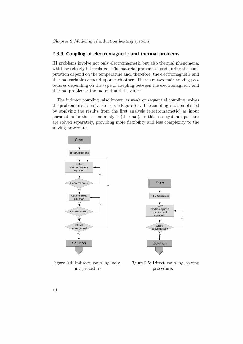
Chapter 2 Modeling of induction heating systems
2.3.3 Coupling of electromagnetic and thermal problems
IH problems involve not only electromagnetic but also thermal phenomena,which are closely interrelated. The material properties used during the com-putation depend on the temperature and, therefore, the electromagnetic andthermal variables depend upon each other. There are two main solving pro-cedures depending on the type of coupling between the electromagnetic andthermal problems: the indirect and the direct.
The indirect coupling, also known as weak or sequential coupling, solvesthe problem in successive steps, see Figure 2.4. The coupling is accomplishedby applying the results from the first analysis (electromagnetic) as inputparameters for the second analysis (thermal). In this case system equationsare solved separately, providing more flexibility and less complexity to thesolving procedure.
Initial Conditions
Start
Solve thermal equation
No
Solve electromagnetic
equation
Convergence ?
No
Convergence ?
Global convergence?
No
Solution
Yes
Yes
Yes
Yes
Figure 2.4: Indirect coupling solv-ing procedure.
Initial Conditions
Solve electromagnetic
and thermalequations
Global convergence?
No
Yes
Figure 2.5: Direct coupling solvingprocedure.
26

ii
“PhD” — 2012/5/21 — 8:58 — page 27 — #32 ii
ii
ii
2.4 Summary
The direct or strong coupling solves simultaneously both system equationsconsidering all the variables, see Figure 2.5. In this case, the electromagneticand thermal unknown parameters are part of the global matrix used to solvethe problem. It is much more complex and is just used when there is ahigh interaction between both problems and the processes have similar timeconstants.
Considering that usually time constants of the electromagnetic and ther-mal processes are different, for most IH applications the indirect coupling isvalid.
2.4 Summary
In this chapter, different methods of modeling IH systems are presented.First of all, the analytical methods are introduced, presenting a more com-plex analytical method with an equivalent circuit based on 5 parameters.These parameters are the workpiece resistance(Rw), the coil resistance (Rc),the gap inductance (La), the workpiece inductance (Lw) and the coil induc-tance (Lc). Regarding the electrical efficiency, this model presents a similarbehavior to the model presented in Section 1.3.
Analytical methods are simple and rough methods of calculation used be-fore, that allow dealing with simple geometries using materials with constantproperties. Even they use and results are very limited, they can serve for afirst approach for power converter designers in case of not having appropri-ate numerical simulation softwares. However, in case of needing an accurateand precise analysis it is mandatory to use numerical methods.
The emergence of high performance computers and the decrease of theircost have facilitated the incorporation of numerical methods in IH industry.Nowadays, the development of commercial softwares is favoring the adoptionof numerical methods by IH designers.
In IH applications, numerical methods are usually based on the resolu-tion of Maxwell equations assuming the magnetoquasistatic approximationand using their harmonic form. There are many methods of solving theseequations classified in two main groups: differential and integral methods.In the differential methods are included the FDM and the FEM, and in theintegral methods the BEM. There is not an unique resolution method for allthe cases. Depending on the application, one method, another or their com-bination may be preferable. It has to be noted that in IH the combinationof thermal and electromagnetic problems pose a difficulty. Concerning this,
27

Chapter 2 Modeling of induction heating systems
the coupling of both problems can be direct or indirect, although in mostapplications the indirect coupling is suitable.
Although numerical methods are becoming more and more popular andplay an important role in IH, there are still some barriers for their incorpo-ration in small and medium research groups and enterprises. The usabilityof commercial softwares has improved clearly in last years, becoming muchmore intuitive and user friendly. However, their complexity still require ofhighly skilled staff completely devoted to the resolution of these problems.Anyway, it has to be stressed that 1D softwares for not so highly skilledstaff exist, an example of that is Elta c©, with which is possible to realize ananalysis in few minutes and starting from zero. Another barrier for the useof these softwares in small and medium laboratories and enterprises startingin this field is their cost.
28

ii
“PhD” — 2012/5/21 — 8:58 — page 29 — #33 ii
ii
ii
Chapter 3
Induction heating converters
3.1 Introduction
In IH, the heat is generated by eddy currents which are originated by a vary-ing magnetic field that is obtained by means of a varying current circulatingin an inductor, as shown in Chapter 1. To have a high varying current inthe inductor, most authors tend to use an oscillatory circuit formed by theinductor and a capacitor in series or in parallel. This oscillatory circuit, alsoknown as resonant tank, is usually fed by a converter, whose characteristicsdepend on the frequency, the power and the type of resonant tank.
IH converters belong to the so-called load-resonant converters family, [21,p. 249]. Commutating at resonant frequency allows having more efficientequipments, which may be essential in some high frequency applications,although the main reason is that permits having higher currents in the in-ductor.
There are many criteria to make a classification of IH converters, forexample the one presented in [2, p. 637]. One common criteria is classifyingthe converters according to the type of resonant tank, where the most basictopologies are those based on series and parallel tanks, as shown in Figu-re 3.1. The converters associated to these tanks are the voltage-fed seriesresonant inverters (VFSRI) and the current-fed parallel resonant inverters(CFPRI) respectively. In most IH applications, the converters used derivefrom them.
In this chapter, the basic concepts and main topologies regarding IH con-verters are introduced. Firstly, VFSRI and the CFPRI structures and theirtanks are extensively presented in Sections 3.2 and 3.3, as they representthe base for understanding other structures and the main concepts used inIH field. First of all with the ideal circuit and afterwards some additionalconsiderations are given. Next, an overview of other structures, as well astheir basic bibliography, is provided in Section 3.4. Finally, the main ideas
29

Chapter 3 Induction heating converters
Req
L
C
Req
L
Inductor-workpiece
C
u(t) i(t)
Inductor-workpiece
Figure 3.1: Series and parallel tank.
of this chapter are summarized in Section 3.5, summing up in a table thedifferences between VFSRI and CFPRI.
For the sake of simplicity, the inductor-workpiece system is modeled dur-ing the whole chapter by a constant resistance and inductance in series. Thisassumption is based on the model described in Chapter 1.
3.2 Voltage-fed series resonant inverters
In series resonant tanks, the inductor is connected in series with the capaci-tor. In this case, the tank behaves as a current source and the inverter usedis a voltage-fed inverter, which means that the inverter is fed with a constantvoltage source. This implies that the inverter is fed by a capacitor with ahigh capacitance value that maintains the voltage constant. In Figure 3.2,a series tank and an ideal VFSRI are shown.
In most applications above 5 kW, the inverter used is the H-bridge [22], asshown in Figure 3.2. This topology is used because allows transmitting thesame power with less current for a given voltage Ue [21, p. 319]. Consideringthat the application of this study is the industrial heating of round wires,where the converters have a power of more than tens of kilowatts, the H-bridge structure is the most commonly found. This is the reason why theH-bridge is the inverter used during the whole study.
In voltage-fed inverters, two switches of the same inverter leg cannot beturned-on at the same time, otherwise short-circuit occurs. The time be-tween the turning-off of one of these switches and the turning-on of the
30

ii
“PhD” — 2012/5/21 — 8:58 — page 31 — #34 ii
ii
ii
3.2 Voltage-fed series resonant inverters
Voltage-fed series resonant inverterSeries tank
Req
L
C
uC
+ -+
+-
-
utank
itank
utank
itank
UeReq
L
Series resonant tank
C
+ -+
+-
-
Voltage-fed inverter
uR
uL
uC
uReq
uL
SW3 SW4
SW2D1
D3
D2
D4
SW1
Inductor-workpiece
Figure 3.2: Series tank and a VFSRI.
other is called dead-time. In this topology, antiparallel diodes are neces-sary to allow inductor’s current conduction when the opposite switches areturned-off.
The most representative methods of controlling the power in VFSRI areexposed in Section 3.4.3. However, during this section, it is assumed thatswitches SW1 & SW4 and SW2 & SW3 commutate alternatively with aduty-cycle of 50 % and the power is controlled by varying the voltage of thesource Ue shown in Figure 3.2.
In the following sections, some concepts regarding the converter’s oper-ation and control are introduced. Firstly, in Sections 3.2.1 and 3.2.2, thedefinition of resonant frequency and the influence of the quality factor inVFSRI are presented. After this, in Section 3.2.3, the basic equations forcalculating the power transmitted to the workpiece are shown. Afterwards,in Section 3.2.4, the sequence of events and implications when commutatingat resonant frequency and out of resonance are explained. Finally, in Sec-tion 3.2.5, some additional considerations are given regarding the inductiveswitching, the semiconductors and the matching transformer needed in mostof VFSRI.
3.2.1 Resonant frequency
The resonant frequency ωr is defined as the frequency at which the maximummodule of a transfer function occurs [23, p. 544].
Observing the RLC circuit of a VFSRI in Figure 3.2, the following equa-
31

Chapter 3 Induction heating converters
tion is accomplished
utank = uReq + uL + uC = Reqitank + Lditankdt
+1
C
∫itankdt (3.1)
Using Laplace transformation with initial conditions equal to zero, Equa-tion 3.1 becomes
Utank(s) = ReqItank(s) + sLItank(s) +1
sCItank(s) (3.2)
obtaining the following second order system with a zero
Hs(s) =Itank(s)
Utank(s)=
sC
s2LC + sCReq + 1= sC
w2n
s2 + 2ζωns+ ω2n
(3.3)
The roots of this second order system are
s1, s2 = −ζωn ± jωn√
1− ζ2 (3.4)
where [23, p. 390]
• ωn is the undamped natural frequency of the system, which is theradial distance of the roots to the origin of the s-plane and is equal to
ωn =1√LC
(3.5)
• ζ is the damping ratio, which is the cosine of the roots to the negativereal axis of the s-plan and is equal to
ζ =Req2
√C
L=
Req2ωnL
(3.6)
Transferring Equation 3.3 to the frequency domain, the transfer functionHs(s) becomes
Hs(s)|s=jω =jωC
1− ω2LC + jωCReq(3.7)
that has the following module
|Hs(ω)| = C√(CReq)2 + (ωLC − 1
ω )2(3.8)
32

ii
“PhD” — 2012/5/21 — 8:58 — page 33 — #35 ii
ii
ii
3.2 Voltage-fed series resonant inverters
Calculating the derivative of Equation 3.8, the next equation is obtained
d |Hs(ω)|dw
= C
[−1
2
[(CReq)
2 + (ωLC − 1
ω)2
]−32[2ωL2C2 − 2
1
ω3
]](3.9)
that has a zero at
ωr =1√LC
(3.10)
being this zero the maximum of Equation 3.3 and, thus, the resonant fre-quency of the circuit.
In this case, the resonant frequency ωr is equal to the undamped naturalfrequency ωn and the transfer function at this frequency is equal to
Hs(ωr) =Itank(ωr)
Utank(ωr)=
1
Req(3.11)
It has to be noted that the frequency in rad/s (denoted by ω) and in Hz(denoted by f) is used indistinctly. The relation between these frequenciesis ω = 2πf and their subindex is used to distinguish the referred frequency(e.g ωr and fr correspond to the resonant frequency).
In Figure 3.3, the Bode analysis of the transfer function Hs(ω) is shown.In this case, the tank is composed of an Req of 1558 mΩ, an L of 9.78 µHand a C of 0.26 µF . Observing this figure, there is an unique maximum atapproximately 100 kHz, corresponding to the resonant frequency. Bearingin mind that Hs(ω) is the inverse of the impedance (see Equation 3.3), theimpedance at resonant frequency is minimum. Therefore, if a voltage with afrequency equal to the resonant frequency feeds the RLC circuit, the currentis maximum and so it is the heat generated in the workpiece. One of thereasons of using these oscillatory circuits in IH applications is that they allowhigh currents using relatively low voltages.
Another thing observed in Figure 3.3 is that, at resonance frequency, theimpedance equals Req. Under these circumstances, the inductive and thecapacitive part cancel each other and the voltage and current are in phase.Thus, the switching losses are theoretically zero because the current is closeto zero during the commutation. This is the reason why IH converters cancommutate at higher frequencies.
This commutation process without losses is generically known as soft-switching, contrarily to the conventional hard-switching, where losses do
33

Chapter 3 Induction heating converters
0
0.2
0.4
0.6
0.8
Mag
nitu
de (
abs)
104
105
106
-90
-45
0
45
90
Pha
se (
deg)
Bode Diagram
Frequency (Hz)
Figure 3.3: Bode analysis of the transfer function Hs(ω) with Req = 1558mΩ, L = 9.78 µH, C = 0.26 µF and fr = 99.8 kHz.
occur. There are two basic switching mechanisms with regards to soft-switching: zero voltage switching (ZVS) and zero current switching (ZCS).ZVS is associated to the turn-on of the switch, that is realized with zero volt-age, while ZCS is associated to the turn-off of the semiconductor, that occurswithout current. These concepts are frequently used during this section andthe following ones to explain the commutation mechanisms occurring in IHconverters.
3.2.2 Quality factor
The quality factor is presented in Section 1.3.1 as the ratio between thereactive and the active power of the inductor-workpiece system. In thissection the relation between this Q factor and the electrical parameters isdiscussed. Firstly, explaining the relation between the quality factor and thecurrent waveform and, secondly, explaining the relation between this factorand the voltage on the tank components.
34

ii
“PhD” — 2012/5/21 — 8:58 — page 35 — #36 ii
ii
ii
3.2 Voltage-fed series resonant inverters
Quality factor and current
Considering that the converter is commutating at resonant frequency, thequality factor, as defined in Section 1.3.1, is equal to
Q =|Prect|Pact
=ωrL
Req=
1
ωrCReq(3.12)
Combining this equation with the definition of damping ratio in Equation3.6 and knowing that the resonant and the natural frequency are equal forthe series tanks, the following equation is accomplished
Q =1
2ζ(3.13)
As the RLC circuit of the tank is a second order system, it becomes moreundamped and oscillatory as the imaginary part of the roots increases andthe real part decreases [23, p. 393]. Therefore, bearing in mind Equation 3.4,ζ has to be smaller than one to have an oscillatory circuit, since in case ofζ < 1 the system is an underdamped system and in case of ζ = 0 the systemis undamped. Taking this into consideration and observing Equation 3.13,the quality factor gives an idea of how damped is a system. The higher theQ value is, the closer to zero is ζ and the more undamped is the system.
In Figure 3.4, a Bode analysis of Hs(ω) (Equation 3.3) for three differentresonant tanks is shown. These circuits have the same inductance (9.78µH) and capacitance (0.26 µF ), but vary in the Req value, that takes thefollowing values: 15.58 Ω, 3.58 Ω and 1.58 Ω. The corresponding values ofQ for these three cases are 0.39, 1.71 and 3.88. In Figures 3.5, 3.6 and 3.7the time response of utank and itank are shown for these three different casescommutating at resonant frequency, where the commutation frequency fswis equal to resonant frequency fr.
In Figure 3.4, it can also be observed how the peak value increases as theQ value increases. This is logical because the peak value is equal to theinverse of Req (see Equation 3.11), whose value decreases.
Observing the time response for these cases in Figures 3.5, 3.6 and 3.7,it can be seen how the current increases with Q and how, in case of Figure3.5, the current is not sinusoidal. Examining these figures and thinking inthe RLC circuit as a tuned filter, the quality factor can also be understoodas a value of how good the filtering at resonant frequency is. Consideringthat the voltage is a square waveform at resonant frequency, if the systemis overdamped (ζ > 1 and Q < 0.5) like in Figure 3.5, the harmonic compo-nents of the current are significant and the current is not sinusoidal. On the
35
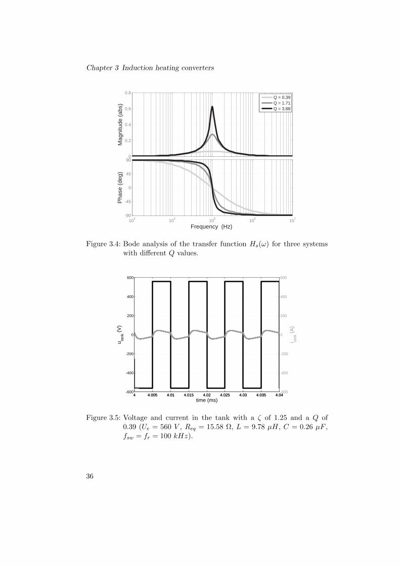
Chapter 3 Induction heating converters
0
0.2
0.4
0.6
0.8
Mag
nitu
de (
abs)
103
104
105
106
107
-90
-45
0
45
90
Pha
se (
deg)
Bode Diagram
Frequency (Hz)
Q = 0.39Q = 1.71Q = 3.88
Figure 3.4: Bode analysis of the transfer function Hs(ω) for three systemswith different Q values.
4 4.005 4.01 4.015 4.02 4.025 4.03 4.035 4.04-600
-400
-200
0
200
400
600
u tank
(V
)
4 4.005 4.01 4.015 4.02 4.025 4.03 4.035 4.04-600
-400
-200
0
200
400
600
i tank
(A
)
time (ms)
Figure 3.5: Voltage and current in the tank with a ζ of 1.25 and a Q of0.39 (Ue = 560 V , Req = 15.58 Ω, L = 9.78 µH, C = 0.26 µF ,fsw = fr = 100 kHz).
36

ii
“PhD” — 2012/5/21 — 8:58 — page 37 — #37 ii
ii
ii
3.2 Voltage-fed series resonant inverters
4 4.005 4.01 4.015 4.02 4.025 4.03 4.035 4.04-600
-400
-200
0
200
400
600
u tank
(V
)
4 4.005 4.01 4.015 4.02 4.025 4.03 4.035 4.04-600
-400
-200
0
200
400
600
i tank
(A
)
time (ms)
Figure 3.6: Voltage and current in the tank with a ζ of 0.29 and a Q of1.71 (Ue = 560 V , Req = 3.58 Ω, L = 9.78 µH, C = 0.26 µF ,fsw = fr = 100 kHz).
4 4.005 4.01 4.015 4.02 4.025 4.03 4.035 4.04-600
-400
-200
0
200
400
600
u tank
(V
)
4 4.005 4.01 4.015 4.02 4.025 4.03 4.035 4.04-600
-400
-200
0
200
400
600i ta
nk (
A)
time (ms)
Figure 3.7: Voltage and current in the tank with a ζ of 0.13 and a Q of3.88 (Ue = 560 V , Req = 1.58 Ω, L = 9.78 µH, C = 0.26 µF ,fsw = fr = 100 kHz).
37

Chapter 3 Induction heating converters
other hand, if the system is underdamped (ζ < 1 and Q > 0.5) the harmoniccomponents are lower and the current is quite sinusoidal, as in Figures 3.6and 3.7.
Therefore, in IH systems is interesting to have a high Q value becausethe current is higher and so it is the heat in the workpiece. Additionally,allows soft-switching during the commutation. For example, in Figure 3.6the system is underdamped (ζ is 0.29 and Q is 1.7), but the Q value is nothigh enough to permit soft-switching at the resonant frequency.
Taking this fact into consideration, it is always interesting to have a highQ value. However, depending on the application, this is not always possiblebecause the value ofQ depends on the equivalent circuit, which is at the sametime determined by the geometries and materials of the inductor-workpiece,as shown in Chapters 1 and 2.
Quality factor and voltage gain
The voltage on the capacitor at resonant frequency accomplishes the nextequation
Uc(ωr) =1
jωrCItank(ωr) (3.14)
As the load is equal to the equivalent resistance (Equation 3.11), com-bining Equation 3.14 with the definition of Q factor (Equation 3.12) andassuming that Utank(ωr) represents the fundamental component of the in-verter output voltage, then
Uc(ωr) =1
jωrC
Utank(ωr)
Req= −jQUtank(ωr) (3.15)
Thus, at resonant frequency, the voltage at the capacitor is Q times thevoltage at the output of the inverter and 90 degrees delayed.
Similarly happens with the inductor voltage, which is equal to
UL(wr) = jωrLItank(ωr) = jωrLUtank(ωr)
Req= jQUtank(ωr) (3.16)
In this case the voltage is Q times the voltage at the output of the inverterbut 90 degrees advanced.
In case of the equivalent resistance, the voltage is equal to the voltage atthe output of the converter
38

ii
“PhD” — 2012/5/21 — 8:58 — page 39 — #38 ii
ii
ii
3.2 Voltage-fed series resonant inverters
UReq(ωr) = ReqItank(ωr) = ReqUtank(ωr)
Req= Utank(ωr) (3.17)
In the previous section, the need of having high Q values has been in-troduced. Nevertheless, considering that the voltage at the capacitor is Qtimes higher, this value has to be limited. For example, having Q valuesover 10, entails having more than 1000 V at the capacitors for 100 V in theoutput of the converter. This implies having more capacitors in series towithstand these voltages, but also paying attention to problems of isolationand security due to the high voltages and frequencies involved. It is very dif-ficult to define a limit for the Q value because it depends on the application.However, IH designers tend to use Q values between 3 and 15.
In the previous section, it was explained that the RLC circuit acts asa filter tuned at the resonant frequency, thus, in most cases, just the firstharmonic is considered. For example, in case of having a Q factor of 3 anda square wave at the output of the inverter, the first harmonic is 24 timeshigher than the next one [24]. Therefore, even though utank is a square wave,it can be simplified to its first harmonic with the following equation
Utank ≈4Ue√
2π(3.18)
being Utank the root mean square (RMS) value of the first harmonic. It hasto be noted that this assumption can be used in Equations 3.15, 3.16 and3.17.
This approximation can be observed in Figure 3.8, where the voltage andcurrent waveforms are shown for a certain tank commutating at resonantfrequency. In this case, the RMS voltage at the resistance UReq is equal to504 V , which coincides with the first harmonic of utank using Equation 7.1with Ue equal to 560 V . The same occurs with the voltage at the capacitorUC , that is 1965 V in RMS and is practically equal to Q times Utank. Addi-tionally, the resistor voltage is in phase with tank voltage and the capacitorvoltage is 90 degrees delayed.
Observing the inductor voltage, uL advances 90 degrees the tank voltage(utank), but the waveform is not sinusoidal. In fact, uL is the sum of asinus (Q times the first harmonic of utank) plus the difference between uReq(sinusoidal) and utank (square wave). In any case, from a practical point ofview, Equation 3.16 can be used as a good approximation.
39

Chapter 3 Induction heating converters
4 4.005 4.01 4.015 4.02 4.025 4.03 4.035 4.04-600
-400
-200
0
200
400
600
u tank
(V
)
4 4.005 4.01 4.015 4.02 4.025 4.03 4.035 4.04-600
-400
-200
0
200
400
600
i tank
(A
)
4 4.005 4.01 4.015 4.02 4.025 4.03 4.035 4.04-4000-3000-2000-1000
01000200030004000
u Re
q
, u C
, u L (
V)
time (ms)
uR
eq
uC
uL
504 V 1965 V
Figure 3.8: Voltage and current in the tank and in the RLC circuit (Ue =560 V , Req = 1.58 Ω, L = 9.78 µH, C = 0.26 µF , fsw =fr =100 kHz, Q = 3.88).
3.2.3 Power in the workpiece
With regard to the power transmitted to the workpiece, it can be easilycalculated considering that Req represents the workpiece resistance (Section1.3.2). Assuming this definition, the power is equal to
P = I2tankReq =
U2Req
Req(3.19)
Bearing in mind that the power is maximum when the current is maxi-mum, the power is maximum at resonant frequency ( Section 3.2.1). Con-sidering that the voltage across the resistance is equal to the first harmonicof utank (Equations 3.17 and 7.1), then
P (ωr) =
(UReq(ωr)
)2Req
=( 4Ue√
2π)2
Req=
8U2e
π2Req(3.20)
It is observed from Equation 3.20, that the power delivered to the work-piece can be controlled by the voltage of the voltage-source Ue. This is themost intuitive power control method, but in Section 3.4.3 other methods arebriefly presented.
In this case, the model of inductor-workpiece explained in Section 1.3 hasbeen used to introduce the manner of calculating the power. However, the
40

ii
“PhD” — 2012/5/21 — 8:58 — page 41 — #39 ii
ii
ii
3.2 Voltage-fed series resonant inverters
analytical model explained in Section 2.2 can also be applied. In that case,the inductance and resistances used for doing the calculations are the sumof them and the power delivered to the workpiece is calculated using Rw.
3.2.4 Commutation analysis
That resonant frequency is the point where the maximum power is givento the workpiece, was explained in previous sections. It was also explainedthat, at this frequency, the commutation occurs when the current is closeto zero, diminishing the commutation losses. However, in real systems isalmost impossible be at perfect resonance, due to small changes in the loador just because there are small inaccuracies in the control system. Therefore,during normal operation the converter is most of time slightly above orunder resonance. These different commutation circumstances are studiedin this section. The aim of this study is to understand the sequence ofevents occurring during the commutation process and disclose the preferablebehavior of the converter.
In Figure 3.9, a simple scheme of a VFSRI that illustrates the variablesused during the explanations is presented. In Figures 3.10, 3.11 and 3.12,the current and the voltage on the tank are shown. The current in SW1and D1, as well as the gate signals of switches, are also plotted to make thesequence of events described below the graph more comprehensible. It hasto be noted that, in case of VFSRI, to avoid short-circuit two switches of thesame inverter leg cannot be conducting at the same time. In this section, thedead-time is neglected and the turn-on and off are supposed ideal, withoutany delay.
Authors would like also to note that the explanations realized in thissection are based on unreal simplifications that serve to introduce the com-mutation states and principles to the reader. However, the explanation ofZVS and ZCS is only reasonable when considering the parasitic components,as it is done in Section 3.2.5.
Commutating at resonant frequency (fsw = fr)
Figure 3.10 shows the corresponding sequence for an inverter commutatingat resonant frequency. In this case, the commutation, illustrated by the gatesignals, occurs when the current is crossing zero. Observing SW1 and itsantiparallel diode, the current is flowing through SW1 half of the cycle andthe diode is never conducting.
41

Chapter 3 Induction heating converters
Ue
Ie
SW3 SW4
SW2
D1
D3
D2
D4
utank
itank
SW1iSW1 iD1
Figure 3.9: VFSRI circuit and variables studied.
0.934 0.936 0.938 0.94 0.942 0.944 0.946 0.948 0.95 0.952-600-400-200
0200400600
u tank
(V
)
0.934 0.936 0.938 0.94 0.942 0.944 0.946 0.948 0.95 0.952-600-400-2000200400600
i tank
(A
)
0.934 0.936 0.938 0.94 0.942 0.944 0.946 0.948 0.95 0.952-600-400-200
0200400600
i SW
1 (A
)
0.934 0.936 0.938 0.94 0.942 0.944 0.946 0.948 0.95 0.952-600-400-2000200400600
i D1 (
A)
0.934 0.936 0.938 0.94 0.942 0.944 0.946 0.948 0.95 0.9520
0.20.40.60.8
1
Gat
e si
gnal
sS
W1
& S
W4
0.934 0.936 0.938 0.94 0.942 0.944 0.946 0.948 0.95 0.95200.20.40.60.81
Gat
e si
gnal
sS
W2
& S
W3
time (ms)
Ue
Ie
SW3 SW4
SW2
D3
D2
D4
State I State II
Soft turn-off of SW2 and SW3 Soft turn-on of SW1 and SW4
SW1
State I
Soft turn-off of SW1 and SW4 Soft turn-on of SW2 and SW3
Ue
SW1
SW3 SW4
SW2D1
D3
D2
D4
itank
State II
State I
State II
State I
Ie
D1
Sequence of events
itank
Figure 3.10: Output waveforms and sequence of events commutating at res-onant frequency (Ue = 560 V , Req = 1.58 Ω, L = 9.78 µH, C= 0.26 µF , fsw = fr = 100 kHz).
42

ii
“PhD” — 2012/5/21 — 8:58 — page 43 — #40 ii
ii
ii
3.2 Voltage-fed series resonant inverters
Under these circumstances there are just two possible states. The firstone, when SW1 and SW4 are conducting and, the second one, when SW2and SW3 conduct. Considering losses, there are no commutation lossesbecause switches commutate when the current is zero.
This is the ideal situation with regards to switching losses, but the prob-ability of being at perfect resonance is low. Thus, the other situations needto be studied.
Capacitive switching (fsw < fr)
In Figure 3.11, the waveforms and the corresponding sequence of eventswhen switching below resonance are shown. Observing this figure, it isnoticed that the commutation and the voltage’s zero crossing, occur afterthe current’s zero crossing. In this case, the current advances the voltage, sothat this type of commutation is called capacitive switching. The relationbetween frequency and current and voltage phase-shift can be observed inthe Bode diagram of Figure 3.3 in Section 3.2.1.
Compared to the previous case, SW1 does not conduct half of the periodand its antiparallel diode is conducting for a short period of time. In fact,D1 is forward-biased after the current’s zero crossing and before the turn-offof SW1. In this case, itank is slightly lower than in the previous case, but thedifference is not noticeable. This difference can also be observed in the Bodediagram of Figure 3.3 where, depending on the Q factor and the frequency,there is a higher or lower decrease on the gain.
Observing the sequence of events in Figure 3.11, in State I the current isflowing through SW1 and SW4. Afterwards, itank changes polarity, whileSW1 and SW4 are turned-on, and diodes D1 and D4 are forward-biasedwith ZVS (State II). Then, SW1 and SW4 are turned-off with ZCS becausetheir antiparallel diodes are conducting (State III). Finally, SW2 and SW3are turned-on hardly, causing the hard turn-off of diodes D1 and D4 (StateIV). In regard to States V and VI, they are similar to States II and III, butwith the opposite switches and diodes.
In this case, diodes’ turn-off and switches’ turn-on are hard, but the turn-on of diodes and the turn-off of switches is soft. One of the problems derivedfrom diodes’ hard turn-off is that large recovery currents can create volt-age spikes. This causes an increase of electromagnetic interferences, lossesand, in the worst case, the destruction of semiconductors. Thus, capacitiveswitching has to be avoided if possible.
43
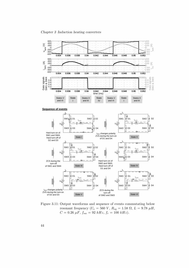
Chapter 3 Induction heating converters
0.934 0.936 0.938 0.94 0.942 0.944 0.946 0.948 0.95 0.952-600-400-200
0200400600
u tank
(V
)
0.934 0.936 0.938 0.94 0.942 0.944 0.946 0.948 0.95 0.952-600-400-2000200400600
i tank
(A
)
0.934 0.936 0.938 0.94 0.942 0.944 0.946 0.948 0.95 0.952-600-400-200
0200400600
i SW
1 (A
)
0.934 0.936 0.938 0.94 0.942 0.944 0.946 0.948 0.95 0.952-600-400-2000200400600
i D1 (
A)
0.934 0.936 0.938 0.94 0.942 0.944 0.946 0.948 0.95 0.9520
0.20.40.60.8
1
Gat
e si
gn
als
SW
1 &
SW
4
0.934 0.936 0.938 0.94 0.942 0.944 0.946 0.948 0.95 0.95200.20.40.60.81
Gat
e si
gn
als
SW
2 &
SW
3
time (ms)
States IIand III
Ue
Ie
SW3 SW4
SW2
D3
D2
D4
State I State II
SW1
State I
Ue
SW1
SW3 SW4
SW2D1
D3
D2
D4
State IV
Ie
D1
Sequence of events
itank changes polarityZVS during the turn-on
of D1 and D4
Ue
Ie
SW3 SW4
SW2
D3
D2
D4
State III State IV
SW1
Ue
SW1
SW3 SW4
SW2D1
D3
D2
D4
itank
Ie
D1
ZCS during theturn-off
of SW1 and SW4
Hard turn-on of SW2 and SW3,Hard turn-off of
D1 and D4
itank itank
itank
States Vand VI
Ue
Ie
SW3 SW4
SW2
D3
D2
D4
State V State VI
SW1
Ue
SW1
SW3 SW4
SW2D1
D3
D2
D4
itank
Ie
D1
Hard turn-on of SW1 and SW4,Hard turn-off of
D2 and D3
itank
itank changes polarityZVS during the turn-on
of D2 and D3
ZCS during theturn-off
of SW2 and SW3
States IIand III
State I
States Vand VI
Figure 3.11: Output waveforms and sequence of events commutating belowresonant frequency (Ue = 560 V , Req = 1.58 Ω, L = 9.78 µH,C = 0.26 µF , fsw = 92 kHz, fr = 100 kHz).
44
ii
“PhD” — 2012/5/21 — 8:58 — page 45 — #41 ii
ii
ii
3.2 Voltage-fed series resonant inverters
Inductive switching (fsw > fr)
Figure 3.12 shows the corresponding waveforms and sequence of events whenthe inverter is commutating above resonant frequency. In this case, thecommutation and the voltage’s zero crossing occur before the current’s zerocrossing. Under these circumstances, the current delays the voltage and thistype of commutation is known as inductive switching.
Similarly to capacitive switching, D1 is forward-biased. But, in this case,D1 conducts after the commutation and before the change of polarity ofitank. The value of itank is also slightly lower than in case of switching atresonant frequency, but the difference is not noticeable.
Observing the sequence of events in Figure 3.12, the current is flowingthrough SW1 and SW4 in State I. Then, switches SW1 and SW4 areturned-off hardly, causing the hard turn-on of D2 and D3 (State II). Im-mediately afterwards, SW2 and SW3 are turned-on with ZVS because thecurrent is flowing through their antiparallel diodes (State III). And finally,itank changes polarity and diodes D2 and D3 are blocked with ZCS becausethe current starts conducting through SW2 and SW3 (State IV). States Vand VI are similar to States II and III, but with the opposite switches anddiodes.
Contrarily to the previous case, diodes’ turn-on and switches’ turn-off ishard, but the turn-off of diodes and the turn-on of switches is soft. Con-sidering the low probability of being at perfect resonance and the problemsderived from the hard turn-off of antiparallel diodes, authors like [25] and [26]suggest working above resonant frequency. Under these circumstances, it hasto be noted that it is mandatory to use switches with unidirectional volt-age capability but bidirectional current capability, thus, using antiparalleldiodes becomes necessary.
3.2.5 Additional considerations
Until the moment, an ideal circuit with ideal sources has been supposed. Thedead-time has been neglected and the parasitic components have been omit-ted. The switches are supposed ideal and no references are given about thecurrent in the converter. However, these parameters need to be consideredduring the design because they determine the converter’s performance.
In this section, the effect of the parasitic capacitors and dead-time on thecommutation and on the switching frequency are considered. Afterwards,some considerations concerning power semiconductors in VFSRI are given.
45
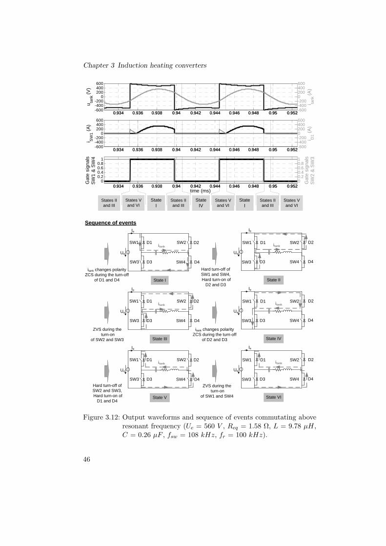
Chapter 3 Induction heating converters
0.934 0.936 0.938 0.94 0.942 0.944 0.946 0.948 0.95 0.952-600-400-200
0200400600
u tan
k (V
)
0.934 0.936 0.938 0.94 0.942 0.944 0.946 0.948 0.95 0.952-600-400-2000200400600
i tank
(A
)
0.934 0.936 0.938 0.94 0.942 0.944 0.946 0.948 0.95 0.952-600-400-200
0200400600
i SW
1 (A
)
0.934 0.936 0.938 0.94 0.942 0.944 0.946 0.948 0.95 0.952-600-400-2000200400600
i D1 (
A)
0.934 0.936 0.938 0.94 0.942 0.944 0.946 0.948 0.95 0.9520
0.20.40.60.8
1
Gat
e si
gnal
sS
W1
& S
W4
0.934 0.936 0.938 0.94 0.942 0.944 0.946 0.948 0.95 0.95200.20.40.60.81
Gat
e si
gnal
sS
W2
& S
W3
time (ms)
States Vand VI
States IIand III
Ue
Ie
SW3 SW4
SW2
D3
D2
D4
State I State II
SW1
State I
Ue
SW1
SW3 SW4
SW2D1
D3
D2
D4
State IV
Ie
D1
Sequence of events
Hard turn-off of SW1 and SW4,Hard turn-on of
D2 and D3
Ue
Ie
SW3 SW4
SW2
D3
D2
D4
State III State IV
SW1
Ue
SW1
SW3 SW4
SW2D1
D3
D2
D4
itank
Ie
D1
ZVS during theturn-on
of SW2 and SW3
itank changes polarityZCS during the turn-off
of D2 and D3
itank itank
itank
States Vand VI
Ue
Ie
SW3 SW4
SW2
D3
D2
D4
State V State VI
SW1
Ue
SW1
SW3 SW4
SW2D1
D3
D2
D4
itank
Ie
D1itank
Hard turn-off of SW2 and SW3,Hard turn-on of
D1 and D4
ZVS during theturn-on
of SW1 and SW4
States IIand III
State I
itank changes polarityZCS during the turn-off
of D1 and D4
States Vand VI
States IIand III
Figure 3.12: Output waveforms and sequence of events commutating aboveresonant frequency (Ue = 560 V , Req = 1.58 Ω, L = 9.78 µH,C = 0.26 µF , fsw = 108 kHz, fr = 100 kHz).
46

ii
“PhD” — 2012/5/21 — 8:58 — page 47 — #42 ii
ii
ii
3.2 Voltage-fed series resonant inverters
Finally, the need of a transformer between the load and the converter dueto the high currents through semiconductors is exposed.
Commutation sequence considering parasitic capacitances anddead-time
In Section 3.2.4, the different sequences of events when switching at resonantfrequency, below and above are explained. Due to the problems derived fromthe reverse recovery currents in diodes, most authors commutate above res-onant frequency. Nevertheless, during these analyses, parasitic capacitancesof semiconductors and dead-times between switches have not been consid-ered. In this section, the influence of these parameters is explained.
In Figure 3.13, the electrical scheme for a VFSRI considering parasiticcapacitances (Cp) is shown. It has to be noted that this capacitance includesthe parasitic capacitance, but also the snubber in case of having it. Assumingthe inverter is switching above resonance, Figure 3.14 shows the outputwaveform and the events considering these capacitances and the dead-timebetween switches. The states shown in this figure are related to those definedin Figure 3.12 .
Observing Figure 3.12, the sequence that accomplishes soft-switching incase of inductive switching is shown. The sequence of events occurring inthis figure is the following:
1. Switches SW2 and SW3 turn-off hardly.
2. The parasitic capacitance Cp of SW2 and SW3 charge, while Cp ofswitches SW1 and SW4 discharge, increasing the voltage of utank upto Ue.
3. The antiparallel diodes D1 and D4 are forward-biased when utankexceeds Ue.
4. Switches SW1 and SW4 are turned-on with ZVS (their antiparalleldiodes are conducting).
5. The current itanc changes polarity, conducting through SW1 and SW4and turning-off with ZCS the antiparallel diodes D1 and D4.
So far, it was supposed that ZVS during switches’ turn-on and ZCS duringdiodes’ turn-off always occurred when switching above resonance. However,observing Figure 3.14, it is noticed that ZVS and ZCS do not always occur.
47

Chapter 3 Induction heating converters
e
e
utank
itank
p
Figure 3.13: VFSRI considering parasitic capacitances Cp.
utank equals Ue
Diodes D1 and D4 start conducting
Ue
itank
utank
t
State IV State V State VI State I
itank reacheszero and D1 andD4 turn-off softly
Hard turn-off of SW2 and SW3
SW1 and SW4 areturned-on in ZVS
0
t
Gate signals SW1 and SW4
Gate signals SW2 and SW3
β
utank reacheszero
φ
t0 t1
Figure 3.14: Output waveforms and sequence to have ZVS and ZCS commu-tating above resonance.
48

ii
“PhD” — 2012/5/21 — 8:58 — page 49 — #43 ii
ii
ii
3.2 Voltage-fed series resonant inverters
For example, in case of low dead-times, SW1 and SW4 turn-on before utankreaches Ue and there is not ZVS. This situation can occur if the capacitanceCp is high and lasts more than the dead-time to be charged. Another ex-ample is the case in which the phase-shift between voltage and current islow and the current changes polarity before SW1 and SW4 turn-on. In thiscase, there is neither ZVS nor ZCS.
Under real circumstances, the combination of Cp, current, phase-shift anddead-time determine the type of commutation. Different combinations ofthese parameters and the resulting output waveforms are shown in [27] andmore in detail in [28]. A brief resume and the basic equations, includingthose shown in this section, are found in Appendix B. Considering this, theconditions to obtain the correct sequence described above are
β ≥ arccos[1− 2UeCpω
itank
](3.21)
and
ϕ ≥ arccos[1− UeCpω
itank
](3.22)
where (see Figure 3.14)
• β, is the phase-shift between the instant at which the gate signal of theswitch becomes low and the moment at which itank changes polarity.
• ϕ is the phase-shift between utank and itank.
• itank is the amplitude of itank.
• Ue is the voltage of the DC source, as shown in Figure 3.13.
• Cp is the sum of the parasitic capacitance and the snubbers of theswitches.
Observing Equations 3.21 and 3.22, it is observed that the control neededto accomplish a correct commutation process is complex. Furthermore, incase of low currents or high capacitances, β and ϕ are high. Under thesecircumstances, the switching frequency and the reactive power supplied bythe inverter increase and, for providing the same active power, the voltageUe needs to be higher.
49
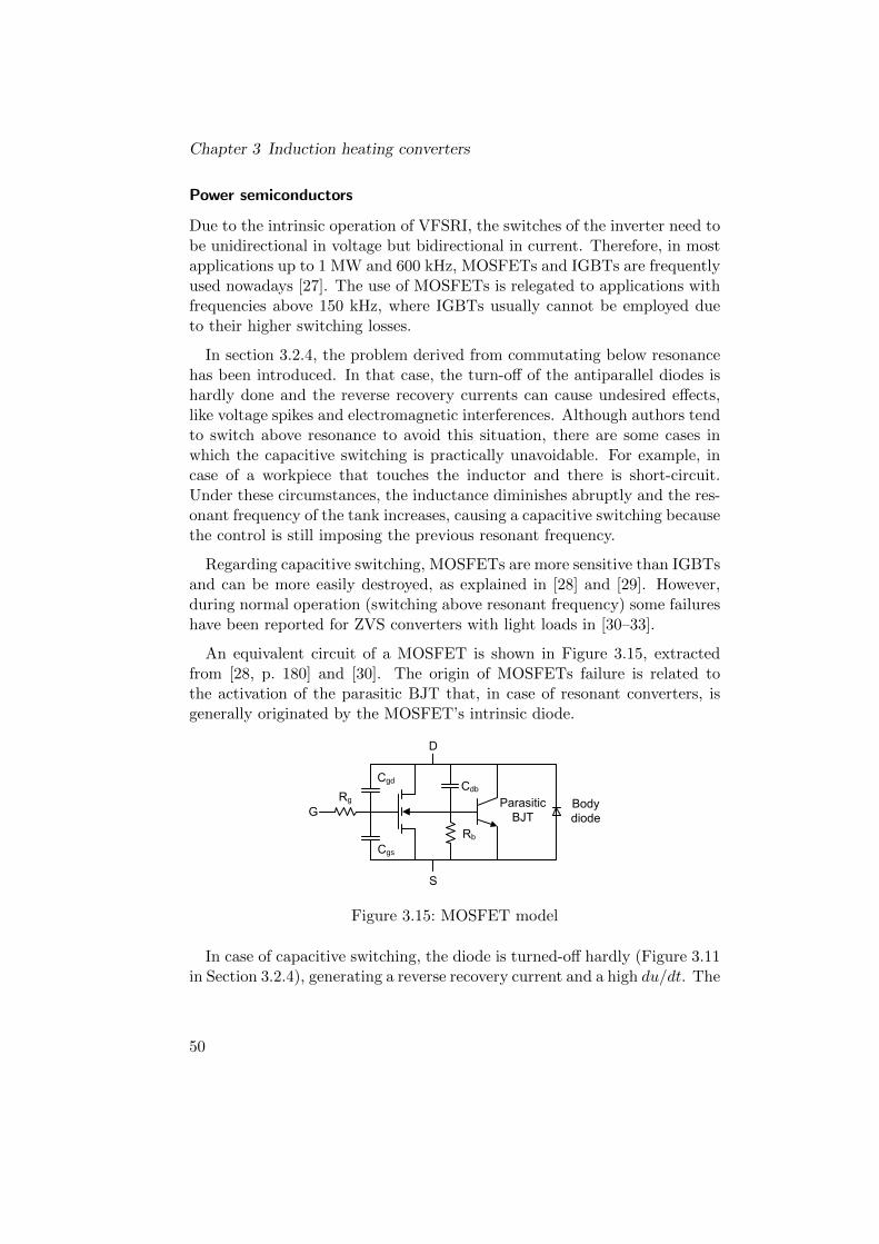
Chapter 3 Induction heating converters
Power semiconductors
Due to the intrinsic operation of VFSRI, the switches of the inverter need tobe unidirectional in voltage but bidirectional in current. Therefore, in mostapplications up to 1 MW and 600 kHz, MOSFETs and IGBTs are frequentlyused nowadays [27]. The use of MOSFETs is relegated to applications withfrequencies above 150 kHz, where IGBTs usually cannot be employed dueto their higher switching losses.
In section 3.2.4, the problem derived from commutating below resonancehas been introduced. In that case, the turn-off of the antiparallel diodes ishardly done and the reverse recovery currents can cause undesired effects,like voltage spikes and electromagnetic interferences. Although authors tendto switch above resonance to avoid this situation, there are some cases inwhich the capacitive switching is practically unavoidable. For example, incase of a workpiece that touches the inductor and there is short-circuit.Under these circumstances, the inductance diminishes abruptly and the res-onant frequency of the tank increases, causing a capacitive switching becausethe control is still imposing the previous resonant frequency.
Regarding capacitive switching, MOSFETs are more sensitive than IGBTsand can be more easily destroyed, as explained in [28] and [29]. However,during normal operation (switching above resonant frequency) some failureshave been reported for ZVS converters with light loads in [30–33].
An equivalent circuit of a MOSFET is shown in Figure 3.15, extractedfrom [28, p. 180] and [30]. The origin of MOSFETs failure is related tothe activation of the parasitic BJT that, in case of resonant converters, isgenerally originated by the MOSFET’s intrinsic diode.
db
b
gd
gs
g
Figure 3.15: MOSFET model
In case of capacitive switching, the diode is turned-off hardly (Figure 3.11in Section 3.2.4), generating a reverse recovery current and a high du/dt. The
50
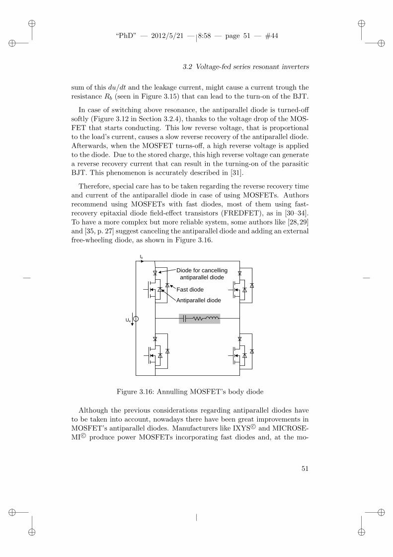
ii
“PhD” — 2012/5/21 — 8:58 — page 51 — #44 ii
ii
ii
3.2 Voltage-fed series resonant inverters
sum of this du/dt and the leakage current, might cause a current trough theresistance Rb (seen in Figure 3.15) that can lead to the turn-on of the BJT.
In case of switching above resonance, the antiparallel diode is turned-offsoftly (Figure 3.12 in Section 3.2.4), thanks to the voltage drop of the MOS-FET that starts conducting. This low reverse voltage, that is proportionalto the load’s current, causes a slow reverse recovery of the antiparallel diode.Afterwards, when the MOSFET turns-off, a high reverse voltage is appliedto the diode. Due to the stored charge, this high reverse voltage can generatea reverse recovery current that can result in the turning-on of the parasiticBJT. This phenomenon is accurately described in [31].
Therefore, special care has to be taken regarding the reverse recovery timeand current of the antiparallel diode in case of using MOSFETs. Authorsrecommend using MOSFETs with fast diodes, most of them using fast-recovery epitaxial diode field-effect transistors (FREDFET), as in [30–34].To have a more complex but more reliable system, some authors like [28,29]and [35, p. 27] suggest canceling the antiparallel diode and adding an externalfree-wheeling diode, as shown in Figure 3.16.
Ue
Ie
Fast diode
Diode for cancelling antiparallel diode
Antiparallel diode
Figure 3.16: Annulling MOSFET’s body diode
Although the previous considerations regarding antiparallel diodes haveto be taken into account, nowadays there have been great improvements inMOSFET’s antiparallel diodes. Manufacturers like IXYS c© and MICROSE-MI c© produce power MOSFETs incorporating fast diodes and, at the mo-
51

Chapter 3 Induction heating converters
ment, silicon carbide technologies are starting to emerge with the promise ofdiodes without reverse recovery currents. In fact, this new silicon technol-ogy has been used already to improve diodes’ turn-on characteristics in [29].However, although there have been great improvements, one of the main dif-ficulties is still the selection of the appropriate MOSFET with its antiparalleldiode just from datasheets information, as stated in [36].
For high frequencies, another important fact considering VFSRI and thesemiconductor’s selection criteria, are the switching losses. Taking into ac-count that VFSRI at inductive switching has minimum turn-on losses buthigher turn-off losses, one of the main parameters affecting the selectionof the device are precisely the turn-off losses. In this case, it is also diffi-cult to make a comparison between devices just considering their datasheetsand experimental tests need to be realized to have an accurate analysis, asexplained in [26].
Matching transformers and VFSRI
In IH, having high current values in the inductance is interesting becausemore heat is produced in the workpiece. However, in case of VFSRI, thecurrent in the tank itank is the same than in the inverter. Considering thatthe value of the equivalent resistance is usually lower than one ohm, thevoltages in the inverter are low and the currents high. From the inverter’spoint of view, the use of low voltages and high currents produce much morelosses and voltage drops.
At the beginning, this was the main limiting problem of VFSRI topologyfor IH converters with semiconductors and one of the reasons of CFPRI pro-liferation. However, nowadays, the developments in materials science andmanufacturing have permitted the appearance of high performance trans-formers. These matching transformers allow the use of VFSRI topology inmany applications, although making the final product more expensive andlowering the efficiency of the system. Nevertheless, it is worth pointing outthat transformers efficiency is usually higher than 95 %. In Section 3.4.2,more details are given considering topologies with matching transformers.
3.3 Current-fed parallel-resonant inverters
In case of parallel tanks, the inductor is connected in parallel with the ca-pacitor. Contrarily to a series connection, the tank behaves like a voltagesource and the inverters used are current-fed. This implies that the inverter
52

ii
“PhD” — 2012/5/21 — 8:58 — page 53 — #45 ii
ii
ii
3.3 Current-fed parallel-resonant inverters
is fed with a high inductance that maintains the current and behaves as aconstant current source. A parallel tank and an ideal CFPRI are shown inFigure 3.17. For the same reasons than for VFSRI, explained in Section 3.2,the inverter used all-along this section is the H-bridge.
In case of current-fed inverters, the current path cannot be opened andswitches from the same inverter leg have to overlap. Switches have to beunidirectional in current but bidirectional in voltage. If diodes are not added,the capacitor would discharge, so Figure 3.17 shows a diode in series with aswitch.
Similarly to VFSRI, CFPRI has different ways of controlling the power.During this section, it is assumed that the power is controlled by varyingthe current of the source (Ie in Figure 3.17) and, thus, that switches SW1& SW4 and SW2 & SW3 commutate alternatively with a duty-cycle of 50%. The inductor-workpiece is also modeled by a constant resistance andinductance in series.
utank
itank
Req
L
Parallel resonant tank
+
+-
-
Current-fed inverter
uReq
uL
SW1
Citank utank
Req
L
+
+-
-
uR
uL
Inductor-workpiece
IeC
iC
iL
iC
iL
D1
SW2
D2
SW3
D3
SW4
D4
Figure 3.17: Parallel tank and a CFPRI.
In the following sections, some concepts regarding CFPRI performanceare introduced. In order to facilitate the comprehension, the distribution ofsections and symbols are similar to the ones used during VFSRI explana-tions. First, in Section 3.3.1, the resonant frequency is found for the caseof para-llel tanks, expressing the resemblances with series tanks for highquality factors. Next, in Section 3.3.2, the quality factor and its influencein voltage waveforms is presented. The relation between currents in thetank and in their components, determined by the quality factor, is also ex-plained. Afterwards, in Section 3.3.3, the basic equations for calculating the
53

Chapter 3 Induction heating converters
power transmitted to the workpiece are shown. After, in Section 3.3.4, theimplications of commutating at zero phase-shift, above and below are ex-plained. Finally, in Section 3.3.5, some considerations regarding the optimalcommutation procedure and overvoltage protections are presented.
3.3.1 Resonant frequency
Proceeding like in VFSRI but for CFPRI, the RLC circuit in Figure 3.17accomplishes the following equations
itank = iC + iL (3.23)
iC = Cdutankdt
(3.24)
iL =1
L
∫uLdt (3.25)
utank = uL + uReq (3.26)
Using Laplace transformation with initial conditions equal to zero, thefollwing equation is obtained
Itank(s) = IC(s) + IL(s) = sCUtank +Utank
sL+Req(3.27)
obtaining the next second order system with a zero
Hp(s) =Utank(s)
Itank(s)=
sL+Reqs2LC + sCReq + 1
= (sL+Req)w2n
s2 + 2ζωns+ ω2n
(3.28)
The roots of this second order system are the same than those found forVFSRI in Equation 3.4. In this case, the same definitions of undampednatural frequency ωn and damping ratio ζ shown in Equations 3.5 and 3.6are used. It has to be noted that in CFPRI the transfer function Hp(s) isequivalent to the impedance, whereas in VFSRI the transfer function Hs(s)is equivalent to the conductance.
Transforming Equation 3.28 into the frequency domain, the followingequation is obtained
54

ii
“PhD” — 2012/5/21 — 8:58 — page 55 — #46 ii
ii
ii
3.3 Current-fed parallel-resonant inverters
Hp(s)|s=ωj =Req
(1− ω2LC)2 + (ωCReq)2
+jω(L− CR2
eq − ω2L2C)
(1− ω2LC)2 + (ωCReq)2
(3.29)
Assuming the definition of resonant frequency as the maximum of a trans-fer function, shown in Section 3.2.1, the mathematical expression is morecomplex for CFPRI than for VFSRI. Proceeding similarly and calculatingthe maximum with the help of mathematical softwares, the maximum ofHp(s) is
ωr =
√C√
2LCR2eq + L2 − C2R2
eq
LC(3.30)
considering the definition of quality factor for the series model of the inductance-workpiece system (Section 1.3.1), Equation 3.30 turns into
ωr = ωn
√√2
Q2+ 1− 1
Q2(3.31)
which is simplified to ωn for high Q values, like in the case of VFSRI.
Considering ωphase0 as the frequency at which the phase-shift betweencurrent and voltage is zero, the imaginary part of Equation 3.29 has to bezero at this frequency. Therefore, ωphase0 is equal to
ωphase0 =
√L− CR2
eq
L2C= ωn
√1− 1
Q2(3.32)
Although Equations 3.31 and 3.32 are different, this difference can beneglected for high Q values, because their values are approximately equal tothe undamped natural frequency ωn.
In Figure 3.18, a Bode analysis of Hp(ω) (Equation 3.28) for different RLCcircuits is shown. The three different circuits have the same inductances(9.78 µH) and capacitances (0.26 µF ), having therefore the same undampednatural frequency ωn . The only difference is the Req value, that takes thefollowing values: 5.58 Ω, 3.58 Ω and 1.58 Ω. The corresponding values of Qfor these three cases are 1.10, 1.71 and 3.88.
55

Chapter 3 Induction heating converters
It can be observed in this figure that the three frequencies ωr, ωphase0 andωn (represented in kHz by fr, fphase0 and fn) are different. But, the higherthe Q value, the more similar they are. In fact, in case of Q equal to 3.88,their values are practically the same with a difference lower than 4 %.
0
5
10
15
20
25
Mag
nitu
de (
abs)
103
104
105
106
-90
-45
0
45
90
Pha
se (
deg)
Frequency (Hz)
Q = 1.10Q = 1.71Q = 3.88
fr = 99.89 kHz
fphase0 = 96.63 kHz
fr = 97.79 kHz
fphase0 = 81.28 kHz
fr = 89.61 kHz
fphase0 = 41.89 kHz
Figure 3.18: Bode analysis of the transfer function Hp(ω) for three systemswith different Q values and fn = 100 kHz.
Assuming that the Q factor is high enough so that these three frequenciesare equal, the impedance Zp(ω) at the resonant frequency ωr is obtained bysubstituting ωn in the module of Equation 3.29. In this case, the followingequation is obtained
Zp(ωr) ≈ |Hp(ωn)| =
√LL+ CR2
eq
C2R2eq
= ReqQ√Q2 + 1 (3.33)
Therefore, the complexity of the equations for CFPRI can be solved byassuming high Q values and simplifying these formulas.
Another simplification, assuming also high Q values, can be done by usingthe parallel model of the inductor-workpiece system explained in Section1.3.1. In this case, the equivalent resistance of the system is supposed to bein parallel with the inductor, as shown in Figure 3.19.
Considering this, the transfer function of the impedance becomes
Hp(s)′ =
Utank(s)
Itank(s)=
sLR′eqs2LCR′eq + sL+R′eq
(3.34)
56

ii
“PhD” — 2012/5/21 — 8:58 — page 57 — #47 ii
ii
ii
3.3 Current-fed parallel-resonant inverters
Citank utank
Req
L
+
+-
-
uR
uL
Inductor-workpiece
iC
iL
Citank utank Req’
++
uR
Inductor-workpiece
iC iL
L
--
uL
iReq’
Figure 3.19: Parallel tank with series and parallel models of inductor-workpiece.
Assuming that the equivalent resistance represents the losses originated bythe eddy currents in the workpiece, the equivalent resistance in the parallelmodel R′eq has to accomplish Equation 1.7.
In Figures 3.20 and 3.21, the Bode analysis for Hp(s) (series model) andHp(s)
′ (parallel model) are shown for two different RLC circuits. The in-ductance (L = 9.78 µH) and the capacitance (C = 0.26 µF ) are the samein both cases, but the resistance varies . The Q value is 1.71 in Figure 3.20(Req = 3.58 Ω and R′eq = 10.46 Ω) and 3,88 in Figure 3.21(Req = 1.58 Ωand R′eq = 23.79 Ω).
Observing these figures, it is noticed that the behavior of both modelsis similar when approaching to the undamped natural frequency fn at 100kHz. It can also be observed how, the higher Q is, the more resemble bothmodels at fn. Therefore, this model can be used as far as the Q value ishigh enough and the analysis is realized in frequencies close to fn.
The benefit of using this parallel model of inductor-workpiece system isthat the resonant frequency ωr, the frequency at which the phase-shift iszero ωphase0 and the undamped natural frequency ωn are equal (Equation3.35).
ωr = ωphase0 = ωn =1√LC
(3.35)
Taking this into consideration, the impedance at resonant frequency isequal to
Zp(ωr)′ =
∣∣Hp(ωr)′∣∣ = R′eq (3.36)
57

Chapter 3 Induction heating converters
0
5
10
15
Mag
nitu
de (
abs)
102
103
104
105
-90
-45
0
45
90
Pha
se (
deg)
Bode Diagram
Frequency (Hz)
Hp()
Hp()'
Figure 3.20: Bode analysis of the transfer function for the series Hp(ω) andparallel Hp(ω)′ models for a system with a Q of 1.71.
0
5
10
15
20
25
Mag
nitu
de (
abs)
102
103
104
105
-90
-45
0
45
90
Pha
se (
deg)
Bode Diagram
Frequency (Hz)
Hp()
Hp()'
Figure 3.21: Bode analysis of the transfer function for the series Hp(ω) andparallel Hp(ω)′ models for a system with a Q of 3.88.
58

ii
“PhD” — 2012/5/21 — 8:58 — page 59 — #48 ii
ii
ii
3.3 Current-fed parallel-resonant inverters
with R′eq = ReqQ2 (Equation 1.7). It has to be noted that this equation is
similar to Equation 3.33 for high Q values.
3.3.2 Quality factor
As in the case of the series resonant tank, the quality factor allows to defineand understand the behavior of the parallel tank. In this section, the rela-tion between the quality factor and voltage is presented and, afterwards, itsrelation within the gain between currents is explained.
Quality factor and voltage
In case of CFPRI, the parallel tank also acts as a tuned filter at resonantfrequency. This can be observed in the Bode diagram of Figure 3.18 inSection 3.3.1. Thus, the only component of the tank voltage utank is due tothe first harmonic of the current square wave itank. In this case, the currentitank is a square waveform and the voltage utank is sinusoidal.
Similarly to VFSRI, the Q factor gives an idea of how good is the filtering.In case of having low Q values, the voltage is not sinusoidal because thereare more harmonic components than the first one and commutating withsoft-switching is not possible. Moreover, in CFPRI, the lower Q is, the moredifferent are ωphase0 and ωr, as shown in Equations 3.31 and 3.32 in theprevious section.
Using the same RLC circuits than in Figure 3.18, the voltage utank andcurrent itank are plotted for Q equal to 1.71 and Q equal to 3.88 in Figures3.22 and 3.23 respectively. In both figures, the switching frequency fsw isequal to fphase0.
In Figure 3.22, the voltage is not sinusoidal and there is a phase-shift be-tween current and voltage. Considering the Bode analysis in Figure 3.18, thepeak of the impedance transfer function Hp is low. Moreover, the resonantfrequency fr and the frequency at which the phase-shift is zero fphase0 aredifferent. Thus, the filtering of the harmonic content is not very good itselfand, as the switching frequency is not the resonant frequency, it becomeseven worse. That is why the phase-shift is not zero and the voltage utank isnot sinusoidal.
Considering the case with a higher Q value, in Figure 3.23, fphase0 andfr are similar and the peak of Hp is higher. Therefore, the filtering is goodenough at the resonant frequency, which is almost the same than fphase0,
59

Chapter 3 Induction heating converters
4 4.005 4.01 4.015 4.02 4.025 4.03 4.035 4.04-1000
-800
-600
-400
-200
0
200
400
600
800
1000
u tank
(V
)
4 4.005 4.01 4.015 4.02 4.025 4.03 4.035 4.04-100
-80
-60
-40
-20
0
20
40
60
80
100
i tank
(A
)
time (ms)
Figure 3.22: Voltage and current in the tank with a Q of 1.71 (Ie = 25 A,Req = 3.58 Ω, L = 9.78 µH, C = 0.26 µF , fsw = fphase0 =81.28 kHz fr = 97.79 kHz and fn = 100 kHz).
4 4.005 4.01 4.015 4.02 4.025 4.03 4.035 4.04-1000
-800
-600
-400
-200
0
200
400
600
800
1000
u tank
(V
)
4 4.005 4.01 4.015 4.02 4.025 4.03 4.035 4.04-100
-80
-60
-40
-20
0
20
40
60
80
100
i tank
(A
)
time (ms)
Figure 3.23: Voltage and current in the tank with a Q of 3.88 (Ie = 25 A,Req = 1.58 Ω, L = 9.78 µH, C = 0.26 µF , fsw = fphase0 =96.63 kHz fr = 99.89 kHz and fn = 100 kHz).
60
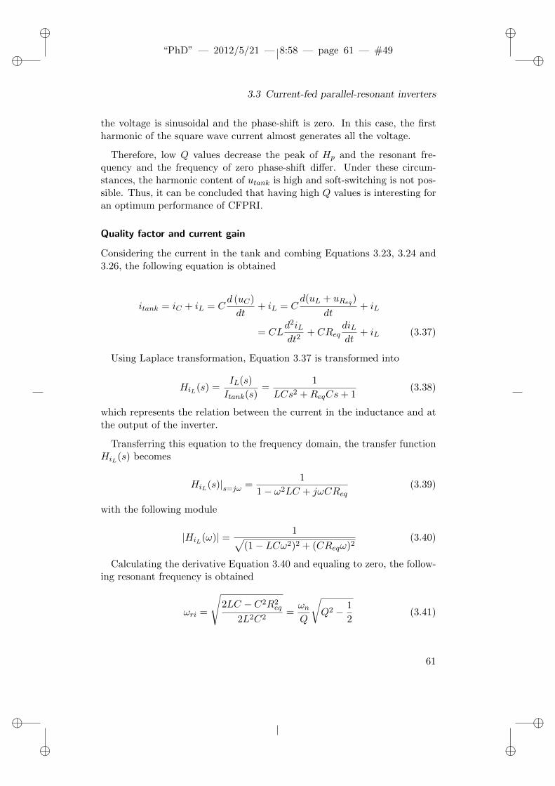
ii
“PhD” — 2012/5/21 — 8:58 — page 61 — #49 ii
ii
ii
3.3 Current-fed parallel-resonant inverters
the voltage is sinusoidal and the phase-shift is zero. In this case, the firstharmonic of the square wave current almost generates all the voltage.
Therefore, low Q values decrease the peak of Hp and the resonant fre-quency and the frequency of zero phase-shift differ. Under these circum-stances, the harmonic content of utank is high and soft-switching is not pos-sible. Thus, it can be concluded that having high Q values is interesting foran optimum performance of CFPRI.
Quality factor and current gain
Considering the current in the tank and combing Equations 3.23, 3.24 and3.26, the following equation is obtained
itank = iC + iL = Cd (uC)
dt+ iL = C
d(uL + uReq)
dt+ iL
= CLd2iLdt2
+ CReqdiLdt
+ iL (3.37)
Using Laplace transformation, Equation 3.37 is transformed into
HiL(s) =IL(s)
Itank(s)=
1
LCs2 +ReqCs+ 1(3.38)
which represents the relation between the current in the inductance and atthe output of the inverter.
Transferring this equation to the frequency domain, the transfer functionHiL(s) becomes
HiL(s)|s=jω =1
1− ω2LC + jωCReq(3.39)
with the following module
|HiL(ω)| = 1√(1− LCω2)2 + (CReqω)2
(3.40)
Calculating the derivative Equation 3.40 and equaling to zero, the follow-ing resonant frequency is obtained
ωri =
√2LC − C2R2
eq
2L2C2=ωnQ
√Q2 − 1
2(3.41)
61

Chapter 3 Induction heating converters
being ωri the frequency at which HiL(ω) is maximum. Thus, ωri is thefrequency that maximizes the current in the inductor for a given itank. Ithas to be noted that ωri is approximately equal to the undamped naturalfrequency ωn for high Q values, like ωr and ωphase0.
Assuming a highQ value, substituting ωn into Equation 3.39 and assumingthat Itank(ωn) represents the fundamental component of the inverter outputcurrent, the gain in current at ωri is approximately
IL(ωri) ≈ IL(ωn) = −jQItank(ωn) (3.42)
Therefore, the current at resonant frequency is Q times the current at theoutput of the inverter and 90 degrees delayed.
Proceeding similarly for the current in the capacitor and combining Equa-tions 3.24 and 3.26 with the transfer function HiL in Equation 3.38, thetransfer function for the current in the capacitor and the current in the tankis
HiC (s) =IC(s)
Itank(s)=
LCs2 + CReqs
LCs2 + CReqs+ 1(3.43)
Transferring this equation to the frequency domain and assuming a highQ value, then
IC(ωri) ≈ IC(ωn) = (1 + jQ)Itank(ωn) (3.44)
Therefore, the current in the capacitor is approximately Q times the cur-rent at the output and 90 degrees advanced.
It can be observed from Equation 3.42 that high Q values are interestingbecause the current in the inductor (and so in the workpiece) is high, whilethe current in the converter is low.
However, the the tank voltage and the capacitors voltage should be studiedcarefully. In Figure 3.17, it can be observed that the voltage utank is thesame than at the capacitors and switches. Considering Equation 3.33, theimpedance is dependent on the square of Q. For a given itank, if the Qis high, the current in the inductance and in the resistance is high too.Thus, the impedance is also high and the voltage utank increases. Therefore,the value of Q has to be high but limited to avoid the destruction of thesemiconductors or an oversized system design.
Taking this fact into consideration, the case of heating steels up to theirCurie temperature deserves special attention. Under these circumstances, µ
62

ii
“PhD” — 2012/5/21 — 8:58 — page 63 — #50 ii
ii
ii
3.3 Current-fed parallel-resonant inverters
decreases and the penetration depth increases, decreasing the Req (Section1.8) and suddenly increasing the Q value and the voltage.
Similarly to VFSRI, but with current, itank can be simplified for high Qvalues to its first harmonic. Thus, itank can be supposed to be equal to
Itank ≈4Ie√2π
(3.45)
being Itank the RMS value of the first harmonic. This simplification can beused in Equations 3.33, 3.42 and 3.44.
In order to see if these assumptions made are correct, Figure 3.24 showsthe voltage and current for the same case shown in Figure 3.18 in Section3.3.1 with Q equal to 3.88. In this case, the current source Ie is set to 25 Aand the system is commutating at fphase0 to avoid switching losses.
4 4.005 4.01 4.015 4.02 4.025 4.03 4.035 4.04-800-600-400-200
0200400600800
u tank
(V
)
4 4.005 4.01 4.015 4.02 4.025 4.03 4.035 4.04-80-60-40-20020406080
i tank
(A
)
4 4.005 4.01 4.015 4.02 4.025 4.03 4.035 4.04-160-120
-80-40
04080
120160
i C,
i L (A
)
time (ms)
iC
iL
538 V
86 A
Figure 3.24: Voltage and current in the tank and in the RLC circuit with aQ of 3,88 (Ie = 25 A, Req = 1.58 Ω, L = 9.78 µH, C = 0.26µF , fsw = fphase0 = 96.63 kHz).
Observing this figure, the current in the capacitor iC is advanced approxi-mately 90 degrees and the current in the inductance iL is delayed 90 degrees,as shown in Equations 3.42 and 3.44. Moreover, using Equation 3.42 andassuming the first harmonic approximation of Equation 3.45, the current inthe inductor is 87 A, which is quite similar to the value obtained during thesimulations in Figure 3.24. It is analogous when using Equation 3.33 for thevoltage, as in this case the voltage obtained is 555 V, whereas in the simu-lations is 538 V. Thus, the assumptions made by considering high Q values
63

Chapter 3 Induction heating converters
show good correspondence with the simulations, with an error smaller than3 % for a Q value of 3.88.
It can be observed that the current in the capacitor iC is not sinusoidal.This is similar to the inductance voltage for VFSRI. In this case, ic is thesum of a sinus (approximately Q times the first harmonic of itank) plus thedifference between iReq (sinusoidal) and itank (square wave). Nevertheless,Equation 3.44 can be used as a good approximation .
3.3.3 Power in the workpiece
Considering that the current in the inductance is the same as in the equiv-alent resistance, the power transmitted to the workpiece is equal to
P = I2LReq (3.46)
Assuming that for high Q values the resonant frequencies ωri and ωr areequal, the current in the equivalent resistance is maximum at the resonantfrequency and so it is the power delivered to the workpiece.
Assuming a high Q value and combining Equation 3.47 with 3.45 and 3.42,the power at resonant frequency is
P (ωr) = IL(ωr)2Req ≈ (QItank(ωn))2Req
≈ (Q4Ie√2π
)2Req =8I2eQ
2Reqπ2
(3.47)
In this case, the power delivered to the wokpiece can be controlled withthe current source Ie.
The model of inductor-workpiece used is the model explained in Section1.3, but the analytical model explained in Section 2.2 can also be applied.In that case, the inductance and resistance are substituted by the sum ofinductances and resistances and the power in the workpiece is calculatedjust with Rw.
3.3.4 Commutation analysis
In previous sections it was explained that, at resonant frequency, the powersupplied to the workpiece is maximum and that the commutation is real-ized with low losses when having high Q values. However, this situation israrely accomplished due to the inaccuracies of the control and the changes
64
ii
“PhD” — 2012/5/21 — 8:58 — page 65 — #51 ii
ii
ii
3.3 Current-fed parallel-resonant inverters
of the parameters during the heating process. Consequently, all the possibleoperation manners have to be studied.
In this section, the cases in which the converter is commutating out ofresonance are studied more in detail. The objective of this study is tocomprehend the sequence of events occurring during the switching processand define the preferable operation for the converter. The explanationsrealized in this section are based on unreal simplifications that serve as anintroduction for the reader. However, the explanation of ZVS and ZCS isonly reasonable when considering the parasitic components, as it is done inSection 3.3.5.
In Figure 3.25, a simple scheme of a CFPRI that illustrates the variablesused during the explanations is presented. In Figures 3.10, 3.11 and 3.12,the current and the across the tank are shown. The voltage across SW1,D1 and the switches’ gate signals are plotted, with the sequence of eventsdescribed below the graph. It has to be noted that, in case of CFPRI, twoswitches of the same inverter leg cannot be opened at the same time as,otherwise, the current circuit is opened and there is an overvoltage. In thiscase, the overlap is the time at which both switches from the same inverterleg are turned-on. In this section, the overlap-time is neglected and theswitching turn-on and off are supposed ideal without any delay.
In the analysis realized in Section 3.2.4 for VFSRI, the resonant frequencyfr is utilized as a reference for that study. In case of CFPRI, the resonantfrequency differs from the frequency at which the phase-shift between cu-rrent and voltage is zero. This is why the frequency chosen as a referencefor this section is fphase0. However, both frequencies, fr and fphase0, arepractically equal for high Q values.
Commutating at zero phase-shift (fsw = fphase0)
Figure 3.26 shows the corresponding sequence considering that the inverteris commutating at zero phase-shift between current and voltage, that is atfphase0. The commutation, illustrated by the gate signals, occurs when thevoltage is crossing zero. Observing the voltage across SW1 and D1, thevoltage is supported by switches half of the cycle while they are turned-off,whereas diodes are always forward-biased.
Under these circumstances, there are just two possible states. The firstis when SW1 and SW4 are conducting and the second when SW2 andSW3 do. Considering the overlapping of switches in current-fed converters,
65

Chapter 3 Induction heating converters
Figure 3.25: CFPRI circuit and variables studied.
0.934 0.936 0.938 0.94 0.942 0.944 0.946 0.948 0.95 0.952-800-600-400-200
0200400600800
u tank
(V
)
0.934 0.936 0.938 0.94 0.942 0.944 0.946 0.948 0.95 0.952-80-60-40-20020406080
i tank
(A
)
0.934 0.936 0.938 0.94 0.942 0.944 0.946 0.948 0.95 0.952-800-600-400-200
0200400600800
uS
W1 (
A)
0.934 0.936 0.938 0.94 0.942 0.944 0.946 0.948 0.95 0.952-800-600-400-2000200400600800
u D1 (
A)
0.934 0.936 0.938 0.94 0.942 0.944 0.946 0.948 0.95 0.9520
0.20.40.60.8
1
Gat
e si
gnal
sS
W1
& S
W4
0.934 0.936 0.938 0.94 0.942 0.944 0.946 0.948 0.95 0.95200.20.40.60.81
Gat
e si
gnal
sS
W2
& S
W3
time (ms)
State I State II
Soft turn-on of SW2 and SW3 Soft turn-off of SW1 and SW4
State I
Soft turn-on of SW1 and SW4 Soft turn-off of SW2 and SW3
State II
State I
State II
Sequence of events
D1 (on)
SW1
D2 (on)
SW2
D3 (on)
SW3
D4 (on)
SW4
Ie
itank
D1 (on)
SW1
D2 (on)
SW2
D3 (on)
SW3
D4 (on)
SW4
Ie
itank
utank+ -
utank
- +utank
Figure 3.26: Output waveforms and sequence of events commutating at zerophase-shift switching (Ie = 25 A, Req = 1.58 Ω, L = 9.78 µH,C = 0.26 µF , fsw = fphase0 = 96.63 kHz).
66
ii
“PhD” — 2012/5/21 — 8:58 — page 67 — #52 ii
ii
ii
3.3 Current-fed parallel-resonant inverters
SW1 and SW4 turn-off is preceded by SW2 and SW3 turn-on, contrarilyto VFSRI.
Regarding losses, this case has very few losses because the commutation isrealized when the current and voltage are zero. Nevertheless, the probabilityof being at this frequency during a long period is low and other cases haveto be studied.
Capacitive switching (fsw > fphase0)
In Figure 3.27, the waveforms and the corresponding sequence of events areshown for the case of switching above fphase0. Observing this figure, thecurrent advances the voltage and so that this type of commutation is alsoknown as capacitive switching. This relation between frequency and currentand voltage phase-shift can also be observed in the Bode diagram, shownin Figure 3.18 in Section 3.3.1. It is worth noticing that contrarily to thiscase, in case of VFSRI, capacitive switching occurs when commutating belowresonance.
Under these circumstances, diodes are blocking between the commutationand the change of polarity of utank. During this period of the time, thevoltage is shared between switches and diodes. This can be observed inFigure 3.27, where the sum of voltages in SW1 and D1 is equal to utank.
Analyzing the sequence of events of Figure 3.27, in State I the currentitank is first conducting through SW1 and SW4. Then, SW2 and SW3 areturned-on while the voltage utank is still positive. Diodes D1 and D4 areforced to block (off state), due to utank, and itank conducts through SW2and SW3 (State II). Afterwards, SW1 and SW4 are turned-off with ZCSbecause their series diodes are blocked (State III). Finally, utank changespolarity and diodes D1 and D4 are forward biased (on state) with ZVS(State IV). States V and VI are similar to States II and III, but with theopposite switches and diodes.
In this case, diodes’ turn-off and switches’ turn-on are hard, but the turn-on of diodes and the turn-off of switches are soft. Similarly to the capacitiveswitching in VFRSI, this situation has to be avoided, otherwise antiparalleldiode’s recovery currents can create large peak voltage spikes.
Inductive switching (fsw < fphase0)
Figure 3.28 shows the waveforms and the corresponding sequence of eventsfor the case of switching below fphase0. In this case, this switching is called
67

Chapter 3 Induction heating converters
0.934 0.936 0.938 0.94 0.942 0.944 0.946 0.948 0.95 0.952-800-600-400-200
0200400600800
uta
nk (
V)
0.934 0.936 0.938 0.94 0.942 0.944 0.946 0.948 0.95 0.952-80-60-40-20020406080
i tank
(A
)
0.934 0.936 0.938 0.94 0.942 0.944 0.946 0.948 0.95 0.952-800-600-400-200
0200400600800
u SW
1 (A
)
0.934 0.936 0.938 0.94 0.942 0.944 0.946 0.948 0.95 0.952-800-600-400-2000200400600800
u D1 (
A)
0.934 0.936 0.938 0.94 0.942 0.944 0.946 0.948 0.95 0.9520
0.20.40.60.8
1
Gat
e si
gnal
sS
W1
& S
W4
0.934 0.936 0.938 0.94 0.942 0.944 0.946 0.948 0.95 0.95200.20.40.60.81
Gat
e si
gnal
sS
W2
& S
W3
time (ms)
States IIand III
State I State II
State I
State IV
Sequence of events
Hard turn-on of SW2 and SW3,Hard turn-off of
D1 and D4
State III State IV
ZCS during theturn-off
of SW1 and SW4
utank changes polarityZVS during the turn-on
of D1 and D4
States Vand VI
State V State VI
utank changes polarityZVS during the turn-on
of D2 and D3
Hard turn-on of SW1 and SW4,Hard turn-off of
D2 and D3
ZCS during theturn-off
of SW2 and SW3
States IIand III
State I
States Vand VI
D1(on)
SW1
D2 (on)
SW2
D3 (on)
SW3
D4 (on)
SW4
Ie
itank
D1(off)
SW1
D2 (on)
SW2
D3 (on)
SW3
D4 (off)
SW4
Ie
itank
utank+ - utank
+ -
-
-+
+-
+-
+
D1 (off)
SW1
D2 (on)
SW2
D3 (on)
SW3
D4 (off)
SW4
Ie
itank
utank+ -
-
-+
+ D1 (on)
SW1
D2 (on)
SW2
D3 (on)
SW3
D4 (on)
SW4
Ie
itank
utank
- +
-
-+
+
D1 (on)
SW1
D2 (off)
SW2
D3 (off)
SW3
D4 (on)
SW4
Ie
itank
utank- +
+
+-
-
D1 (on)
SW1
D2 (off)
SW2
D3 (off)
SW3
D4 (on)
SW4
Ie
itank
utank- +
+
+-
-
State IV
-+
-+
+-
+-
Figure 3.27: Output waveforms and sequence of events commutating abovezero phase-shift frequency (Ie = 25 A, Req = 1.58 Ω, L = 9.78µH, C = 0.26 µF , fsw = 104.63 kHz, fphase0 = 96.63 kHz).
68

ii
“PhD” — 2012/5/21 — 8:58 — page 69 — #53 ii
ii
ii
3.3 Current-fed parallel-resonant inverters
0.934 0.936 0.938 0.94 0.942 0.944 0.946 0.948 0.95 0.952-800-600-400-200
0200400600800
uta
nk (
V)
0.934 0.936 0.938 0.94 0.942 0.944 0.946 0.948 0.95 0.952-80-60-40-20020406080
i tank
(A
)
0.934 0.936 0.938 0.94 0.942 0.944 0.946 0.948 0.95 0.952-800-600-400-200
0200400600800
u SW
1 (A
)
0.934 0.936 0.938 0.94 0.942 0.944 0.946 0.948 0.95 0.952-800-600-400-2000200400600800
u D1 (
A)
0.934 0.936 0.938 0.94 0.942 0.944 0.946 0.948 0.95 0.9520
0.20.40.60.8
1
Gat
e si
gnal
sS
W1
& S
W4
0.934 0.936 0.938 0.94 0.942 0.944 0.946 0.948 0.95 0.95200.20.40.60.81
Gat
e si
gnal
sS
W2
& S
W3
time (ms)
States IIand III
State I State II
State I
State IV
Sequence of events
utank changes polarityZCS during the turn-off
of D2 and D3
State III State IV
ZVS during theturn-on
of SW2 and SW3
Hard turn-off of SW1 and SW4,Hard turn-on of
D2 and D3
States Vand VI
State V State VI
Hard turn-off of SW2 and SW3,Hard turn-on of
D1 and D4
utank changes polarityZCS during the turn-off
of D1 and D4
ZVS during theturn-on
of SW1 and SW4
State I
States Vand VI
D1(on)
SW1
D2 (on)
SW2
D3 (on)
SW3
D4 (on)
SW4
Ie
itank
D1(on)
SW1
D2 (off)
SW2
D3 (off)
SW3
D4 (on)
SW4
Ie
itank
utank+ - utank
- +
+-
+-
D1 (on)
SW1
D2 (off)
SW2
D3 (off)
SW3
D4 (on)
SW4
Ie
itank
utank- +-
+
D1 (on)
SW1
D2 (on)
SW2
D3 (on)
SW3
D4 (on)
SW4
Ie
itank
utank- +
-
-+
+
D1 (off)
SW1
D2 (on)
SW2
D3 (on)
SW3
D4 (off)
SW4
Ie
itank
utank+ -
-
State IV
+
+-
+-+-
+-
-
+
D1 (off)
SW1
D2 (on)
SW2
D3 (on)
SW3
D4 (off)
SW4
Ie
itank
utank+ -
+
+-
-+-
+- -
+
Figure 3.28: Output waveforms and sequence of events commutating belowzero phase-shift switching (Ie = 25 A, Req = 1.58 Ω, L = 9.78µH, C = 0.26 µF , fsw = 104.63 kHz, fphase0 = 96.63 kHz).
69

Chapter 3 Induction heating converters
inductive because the voltage advances the current. It has to be noted that,in case of VFSRI, the inductive switching takes place when commutatingabove resonance.
Similarly to capacitive switching, diodes are blocking during a part of theperiod although, in this case, the blocking occurs between the change ofpolarity of utank and the commutation.
Observing the sequence of events in Figure 3.28, the current itank is con-ducting through SW1 and SW4 in State I. Then, utank changes polarity,blocking D2 and D3 with ZCS because their switches in series are not con-ducting (State II). After this, SW2 and SW3 are turned-on with ZVS be-cause their series diodes are blocking (State III). Finally, SW1 and SW4 areturned-off, causing the forward-biasing of D2 and D3 (State IV). States Vand VI are similar to States II and III, but with the opposite switches anddiodes.
Contrarily to the previous case, diodes’ turn-on and switches’ turn-off arehard, but the turn-off of diodes and the turn-on of switches are soft. Thus,in case of not considering the parasitic components, inductive switching isbetter than capacitive because problems derived from the hard turn-off ofantiparallel diodes are avoided.
It has to be noted that the conclusions extracted during this section arevalid for the ideal assumptions realized. However, under real circumstances,there are more considerations that have to be taken into account. With re-gards to this considerations, Section 3.3.5 considers a more realistic situationwith parasitic inductances and overlapping-time.
3.3.5 Additional considerations
For the time being, an ideal circuit without any parasitic components andneglecting the overlapping-time has been assumed and it has been proventhat inductive switching improves converter’s performance. However, in caseof considering parasitic inductances and overlapping-time, this conclusion isnot correct.
During previous sections, it was assumed that the path for current sourceIe was always closed. However, in real installations, some fail in switches canlead to their opening, causing an overvoltage that can damage the converterseverely.
Among the many considerations that can be realized regarding CFPRI, inthis section just two remarkable considerations are done. The first, regard-
70

ii
“PhD” — 2012/5/21 — 8:58 — page 71 — #54 ii
ii
ii
3.3 Current-fed parallel-resonant inverters
ing the influence of the parasitic inductances and overlapping-times duringcommutation and, the second, regarding the overvoltage protections of CF-PRI.
Commutation sequence considering parasitic inductances andoverlapping-time
In Section 3.3.4, the different sequences of events for an ideal CFPRI werepresented. The conclusion was that inductive switching (switching belowfphase0) improves the operation of the inverter because avoids the reverserecovery currents of diodes, but this fact changes when the parasitic induc-tances and the overlapping-time are taken into consideration.
The electrical scheme for a CFPRI considering the parasitic inductance Lpis shown in Figure 3.29. This inductance represents the sum of the parasiticinductances of the switches, diodes and connections.
Bearing in mind the transition between State III and IV for inductiveswitching, in Figure 3.28, the current changes polarity due to the hard turn-off SW1 and SW4. In case of having a parasitic inductance Lp, this currentvariation generates a voltage between its terminals. The problem is that thisvoltage is added to utank and increases the voltage at switches, situation thatcan lead to the destruction of the semiconductors.
In case of capacitive switching, the parasitic inductances also affect theswitching process. Observing the transition between States I and II in Figure3.27, but considering Lp, the voltage at the inductance’s terminals opposesto the voltage utank. Thus, commutating at capacitive switching provides amore reliable operation of the inverter if considering Lp. Although diodes’reverse recovery currents are still a problem, capacitive switching is preferredin CFPRI.
To have soft-switching in diodes’ turn on and switches’ turn-off in capaci-tive switching when considering parasitic inductances and overlapping-time,the following sequence is needed (Figure 3.30):
1. Switches SW1 and SW4 turn-on. This commutation can be realizedwith ZVS depending on the value of Lp, whose voltage can block theseries diodes.
2. The current itank diminishes and the parasitic inductance Lp changesthe voltage polarity to maintain the current.
71

Chapter 3 Induction heating converters
tank
tank
ep
Figure 3.29: CFPRI considering parasitic inductances Lp.
itank equals Ie, changing of slope Diodes D2 and D3 turn-off
Ieitank
utank
t
State IV State V State VI State I
utank reacheszero and D2 and
D3 turn-on with ZVS
Turn-on of SW1 and SW4
SW2 and SW3 areturned-off with ZCS
0
t
Gate signals SW1 and SW4
Gate signals SW2 and SW3
β´
itank reacheszero
t0' t1'
φ'
Figure 3.30: Output waveforms and sequence to have ZCS and ZVS commu-tating at capacitive switching.
72

ii
“PhD” — 2012/5/21 — 8:58 — page 73 — #55 ii
ii
ii
3.3 Current-fed parallel-resonant inverters
3. The current itank equals Ie, the voltage across the inductance Lp isalmost zero and diodes D2 and D3 are blocked due to utank.
4. Switches SW2 and SW3 turn-off with ZCS because their series diodesare blocked.
5. The voltage utank changes polarity, forward-biasing D2 and D3 withZVS.
Observing Figure 3.30, it is seen that ZVS and ZCS conditions do notalways occur. For example, if the overlapping-time is low, SW2 and SW3are turned-off before itank has reached Ie and there is not ZCS. Anotherexample is the case where the phase-shift between current and voltage islow and the voltage changes polarity before SW2 and SW3 have turned-off.In this case, there is neither ZVS nor ZCS.
The combination of Lp, voltage, phase-shift and dead-time determine ifsoft-switching can be reached or not. Different combinations of these pa-rameters and the resulting output waveforms are shown in [37] and more indetail in [8]. A brief resume and the basic equations, including those shownin this section, are found in Appendix C. Considering this, the conditions toobtain the correct sequence described above are:
β′ ≥ arccos[1− 2IeLpω
utank
](3.48)
and
ϕ′ ≥ arccos[1− IeLpω
utank
](3.49)
where (see Figure 3.30)
• β′ is the phase-shift between the instant at which the gate signal of theswitch becomes high and the moment at which utank changes polarity.
• ϕ′ is the phase-shift between itank and utank.
• utank is the amplitude of utank.
• Ie is the current of the DC source, as shown in Figure 3.29.
• Lp is the sum of the parasitic inductances.
73

Chapter 3 Induction heating converters
Although diodes’ reverse recovery currents are still a problem at capac-itive switching, they are minimized when commutating with the optimumprocess described above, as the current in the diode and the blocking voltageutank are almost zero when is blocked. In fact, [37] suggests commutatingwhen itank reaches 90 % of Ie to avoid diodes’ reverse recovery currents.Under these circumstances, [38] shows that the series diodes can be avoidedbecause the parasitic inductance blocks the capacitor’s voltage. However,the problems derived from any imprecision in the control can destroy thesemiconductors.
Similarly to VFSRI, a control based on the optimum switching presentedabove for CFPRI is limited because of its complexity. Moreover, in caseof high β′ and ϕ′ values, a more reactive power and frequency are needed,increasing inverter losses [39]. Nevertheless, understanding the commutationprocedure allows authors to improve the design and control of IH systems.
Overvoltage protection
In case of CFPRI, overvoltage can occur if the current circuit feeding theinverter is opened, for example if a semiconductor fails and opens. Thisopening can cause an overvoltage and originate a chain reaction destroyingpart of the converter. To avoid it, active crowbar systems appear in figuresof some articles concerning IH applications, like in [40] and [41].
Due to the speed required for these protection systems, some authorssuggest adding capacitors to withstand and retard the first voltage peak,like in [42] and [8, p. 184]. These capacitors permit more time for theactivation of a second and more powerful active protection system. Thissecond protection system is usually a switch connected to a resistor thatburns the energy stored in the inductance feeding the CFPRI. There arevery few authors that have written about this topic, although it is importantbecause of the speed of this failure and the destruction than can cause.
Bearing in mind the importance of reliability in industrial applications,another important fact when considering overvoltage protection in CFPRI,is the need of special drivers for semiconductors. Since most commercial con-verters in medium power applications are nowadays voltage-fed, most driversincorporate their protections systems. Thus, most medium power commer-cial drivers incorporate protection systems in which the driver turns-off theswitch in case of short-circuit. Using these drivers in CFPRI can cause theundesired opening of the current path and the destruction of semiconductors.
74

ii
“PhD” — 2012/5/21 — 8:58 — page 75 — #56 ii
ii
ii
3.4 Other configurations
Therefore, CFPRI tends to use customized drivers, increasing the designingtime of the converter.
3.4 Other configurations
Although VFSRI and CFPRI are the basic configurations used in IH appli-cations, there are plenty of variations based on them. This chapter providesa brief and introductory overview of different configurations existing in thisarea and a primary bibliography on them.
First, in Section 3.4.1, systems based on three element tanks are intro-duced. Next, in Section 3.4.2, converters using transformers to match theload with the inverter are explained. Afterwards, in Section 3.4.3, converterswithout a DC/DC intermediate stage to control the power and the differentpower control techniques are presented. Then, in Section 3.4.4, convertersbased on parallel and series connections of basic inverters are introduced. Fi-nally, in Section 3.4.5, some special applications like dual frequency invertersor multiload inverters are presented.
3.4.1 Inverters with three element tanks
Series and parallel tanks and their associated inverters have some drawbacksthat have led to the investigation of other topologies. In case of VFSRI,the current in semiconductors is the same than in the load, which impliesthe need of a matching transformer between inverter and load, increasingthe cost of the system and decreasing the efficiency. In case of CFPRI, thecurrent in the inverter is Q times lower than in the inductor, but the inverteris current-fed. This makes difficult the use of commercial equipments dueto the overvoltage protection systems needed. Moreover, the cable betweenconverter and tank is critical due to the parasitic inductance that limits thedistance between them. In order to overcome these limitations, IH systemswith three element tanks have been developed.
There are several possibilities concerning tanks with three elements, butthe most popular is the LCL (also called LLC), because it has some advan-tages compared to VFSRI and CFPRI. It is not the aim of this section toprovide a deep view on this structure, but some of the main characteristicsand advantages are described below. The information exposed during thissection is extracted from [39,43–46] and specially from [9] and [47].
An LCL tank is a parallel tank with an inductance Ls in series, as shown inFigure 3.31. LCL systems are the natural evolution of the parallel and series
75

Chapter 3 Induction heating converters
tanks. They use voltage-fed inverters, providing the benefits of commercialdevices and protection systems, and the current in semiconductors is lowerthan in the inductor, like in CFPRI. Other topologies with three elementshave also been studied, but they do not provide any remarkable advantagecompared to classical systems, as explained in [28, pp. 70–77].
utank
itank
UeReq
L
LCL resonant tank
-
+
+-
-
Voltage-fed inverter
uReq
uL
SW3 SW4
SW2D1
D3
D2
D4
SW1
C
+
uC
Ls
iC
iL
Figure 3.31: Voltage-fed inverter with an LCL tank.
The impedance of an LCL tank can be calculated using Laplace transfor-mation, obtaining the following equation
Zlcl(s) =Utank(s)
Itank(s)=s3LsLC + s2LsReqC + s(Ls + L) +Req
s2LC + sCReq + 1(3.50)
The Bode analysis of Equation 3.50 is shown in Figure 3.32. It can beobserved that there are two resonant frequencies, frp and frs . The frequencyfrp is equal to the resonant frequency of the parallel circuit and frs is theresonant frequency of the union with Ls. Usually, converters with an LCLtank commutate slightly above frs.
Regarding the phase-shift between voltage and current, it has to be notedthat, depending on the values of resistance, capacitance and inductance, thesystem can be capacitive between frp and frs. In the case shown in Figure3.32, it is observed that the impedance is always inductive.
LCL tanks have several advantages, basically that the converter is voltage-fed and the current in the heating inductor iL is approximately Ls/L timesthe current itank. However, these tanks have also some disadvantages.
As can be observed in Figure 3.32, the phase-shift between voltage andcurrent at the resonant frequency frs is not zero. Thus, there are more
76

ii
“PhD” — 2012/5/21 — 8:58 — page 77 — #57 ii
ii
ii
3.4 Other configurations
0
5
10
15
20
25
30M
agni
tude
(ab
s)
102
103
104
0
30
60
90
Pha
se (
deg)
Frequency (Hz)
frp = 20.30 kHz
frs = 22.25 kHz
Figure 3.32: Bode analysis of the transfer function Zlcl(ω) with Req = 0.1mΩ, L = 9.78 µH, Ls = 95.37 µH, C = 6 µF and Q = 10.75.
commutation losses and the converter provides reactive power during normaloperation, increasing the current in semiconductors. Another importantdrawback is that this phase-shift is nor constant neither monotonous andthis makes the control of the system more complicated.
To avoid a high reactive power during normal operation, the phase-shiftbetween voltage and current at resonant frequency frs needs to be mini-mized. From [47], the phase-shift at resonant frequency is equal to
ϕlcl (ωrs) = arctan
(Ls/L+ 1
Q
)(3.51)
To minimize the phase-shift ϕlcl, the ratio Ls/L has to be decreased, butthe decrease of Ls/L results in a decrease in the current gain between iLand itank. To overcome this problem, the quality factor Q needs to be high,in [47] is supposed higher than 6. Under these circumstances, Ls/L can behigh and maintain the current gain, while ϕlcl is low. Moreover, for high Qvalues, the system can be controlled by the phase-shift between utank anduc, which is monotonous and approximately 90o at frs.
Another important advantage of LCL tanks is the short-circuit immu-nity thanks to the inductive behavior of the load [47]. Short-circuits causedby the workpiece and the inductor are common in IH applications. In ashort-circuit, the equivalent inductance and resistance diminish and the res-
77

Chapter 3 Induction heating converters
onant frequency increases suddenly, while the commutation frequency re-mains constant. Under these circumstances, the first commutations canbe capacitive or inductive, depending on the conditions. CFPRI requiresovervoltage protection systems to avoid semiconductor’s destruction, as ex-plained in [8, pp. 171–186]. For the case of VFSRI, the problem is withinthe capacitive switching and the reverse recovery currents of diodes. In [28],this problem is deeply investigated for MOSFET inverters, proposing a con-figuration that annuls the antiparallel diode like in Figure 3.16 in Section3.2.5. For LCL, a special control that ensures commutations without ca-pacitive switching is used in [47]. This control technique does not allow theswitches commutate while current is flowing through their opposite switches’antiparallel diodes. These authors explain that LCL improves VFSRI’s per-formance against short-circuits because, using this control technique, LCLsystem can continue without disconnecting the converter. In case of a VF-SRI and using a similar technique, in [28, pp. 271–276] the converter has tobe stopped because, even though the first capacitive commutations can beavoided, at low frequencies the commutations are capacitive.
This advantage has special interest in applications like tube welding, whereshort-circuits occur often during normal operation for short periods of time.However, it has to be noted that VFSRI have proven to be robust to short-circuits by adding fast diodes to MOSFETs. Moreover, IH companies likeEFD Induction R© have converters using IGBTs for tube welding with tech-nical specifications explaining their operation under short-circuits.
In [28, p. 76] the main drawbacks of LCL tanks are exposed, explainingthat the inclusion of Ls adds more losses to the system due the parasiticresistances and that a transformer is usually required. However, this topol-ogy can be useful for certain applications with high Q values. For example,it can be suitable in case of high frequencies, where Ls can be a small airinductor. An interesting discussion about this topology and the design fordifferent applications is found in [47]. During these designs, a minimumand a maximum Q value is considered. This is because the system changesduring a heat treatment and all the possible cases have to be considered.Therefore, finding a global solution using LCL tanks can be difficult in caseof needing to work with different workpieces.
3.4.2 Converters with matching transformers
In Section 3.2.5, the need of a matching transformer between the VFSRIand the resonant tank was introduced. In case of VFSRIs, the transformer is
78

ii
“PhD” — 2012/5/21 — 8:58 — page 79 — #58 ii
ii
ii
3.4 Other configurations
generally necessary to avoid high currents in semiconductors. However, thesetransformers are also used in other topologies to match the load requirementswith the converter’s specifications.
There are two main groups of matching transformers, the active powertransformers and the reactive power transformers. In Figure 3.33 both typesof transformers and their combinations are shown. The figures shown referto a series resonant tank, but both types of transformers are used in parallel,LCL or other resonant tanks.
Series resonant tank with active transformer
Series resonant tank with reactive transformer
Series resonant tank with active and reactive transformers
Figure 3.33: Series tank with matching transformers.
In case of active power transformers, the power transferred from the pri-mary to the secondary is just active power. The aim of this transformer is toincrease the total impedance seen by the inverter and decrease the current insemiconductors. Supposing an ideal transformer with a transfer ratio equalto i and referring the resonant tank to the primary as shown in Figure 3.34,the impedance is equal to
Z ′tank = i2Ztank (3.52)
Thus, the impedance is i2 higher, decreasing the current and the losses inthe primary. For example, in case of VFSRI, the load seen by the converteris equal to i2Req and the power transferred for the transformer at resonantfrequency is just active power.
In case of reactive power transformers, the power transferred from theprimary to the secondary is reactive. Supposing an ideal transformer witha transfer ratio equal to i and referring the resonant tank to the primary asshown in Figure 3.35, the resonant frequency is equal to
79

Chapter 3 Induction heating converters
f ′r =1
2π√L′C ′
=1
2π√Li2C
=fri
(3.53)
and the quality factor
Q′ =2πf ′rL
′
R′eq=
2π fri Li2
Reqi2=Q
i(3.54)
In this case, the frequency and the quality factor are i times lower. Thesetype of transformers are used in low impedance inductors, as in the case ofcoils with few turns, and low frequencies.
Series resonant tank with active transformer
Req
L
Ci:1
Series resonant tank with active transformer refered to the primary
Req i2
L i2
C i2
Figure 3.34: Series tank with active transformer referred to the primary.
Series resonant tank with reactive transformer
Req
L
Ci:1
Series resonant tank with reactive transformer refered to the primary
Req i2
L i2
C
Figure 3.35: Series tank with reactive transformer referred to the primary.
By adding a reactive power transformer, the capacitance and the currentconducted by the capacitors is decreased. For example, in case of a VFSRI,the impedance at resonant frequency is also equal to i2Req, so that thecurrent in the inverter is also decreased. One of the drawbacks of thesetransformers is the high reactive power conducted through them, as beingQ times the active power of the application. Thus, for a 10 kW applicationwith a quality factor of 5, the transformer has to be at least of 50 kVA.
Another important drawback of using active or reactive power transform-ers is the decrease in efficiency. It is also very important to take into account
80
ii
“PhD” — 2012/5/21 — 8:58 — page 81 — #59 ii
ii
ii
3.4 Other configurations
their parasitic inductances, resistances and capacitances depending on theapplication and the frequency. However, it has to be noted that these trans-formers have been improving during the last decades and, at the moment,they parasitic inductances and resistances are low and their efficiencies areover 95 %.
In any case, the best proof of transformers’ usefulness is that nowadaysmatching transformers are widely used in IH applications. For example, aseries resonant tank and active transformers can be found in [28, 35, 40, 48–56]. Some examples with reactive transformers and series tanks are [57–59]and with parallel tanks and reactive transformers are [60–62]. In [47] an LCLtank with active transformer, reactive transformer and with a combinationof them is explained.
There are various specific companies developing matching transformersfor IH applications, being two of the most well-known CELEM and JacksonTransformers, and some not so specific, like STS. Most of them providedifferent taps to vary the transformer ratio. For a better knowledge in thedesign of these transformers, [2, pp. 656–673] provides a short overview onthe materials and core shapes used.
3.4.3 Converters without intermediate power control stage
In previous sections it was assumed that the inverter was commutating nearresonant frequency with a 50 % of duty-cycle. Under these circumstances,the power supplied to the workpiece is controlled by means of a variableDC source. Traditionally, a conventional thyristor bridge rectifier has beenused to obtain these variable DC source, as shown in Figure 3.36 in Case1. However, this implies an increase in cost and size of the converter dueto the six controlled thyristors and the low frequency inductance needed.At this moment, this topology is only employed for high power convertersabove hundreds of kVA.
Other solutions with reduced cost and complexity have been developed tohave a variable DC source, as for example a diode rectifier with a DC/DCconverter, shown in Figure 3.36 in Case 2. In this case, a DC/DC struc-ture with just one switch like a buck converter can be used. However, theinclusion of this DC/DC intermediate stage decreases the efficiency of theoverall system until values typically between 70 to 90 %. It has to be notedthat, in case of CFPRI with a structure like in Case 1 in Figure 3.36 usingthyristors, the choke feeding the inverter has to be high to maintain thecurrent constant, increasing the size and cost of the equipment. In case of
81
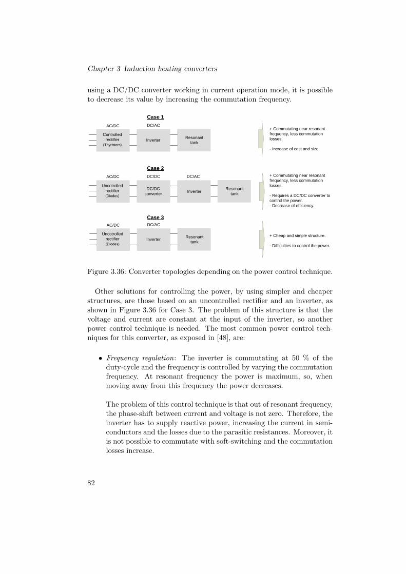
Chapter 3 Induction heating converters
using a DC/DC converter working in current operation mode, it is possibleto decrease its value by increasing the commutation frequency.
Controlled rectifier
(Thyristors)Inverter
Resonant tank
AC/DC DC/AC
Uncotrolled rectifier(Diodes)
DC/DC converter
Resonant tank
AC/DC DC/DC
Inverter
DC/AC
Uncotrolled rectifier(Diodes)
InverterResonant
tank
AC/DC DC/AC
+ Commutating near resonant frequency, less commutation losses.
- Increase of cost and size.
+ Commutating near resonant frequency, less commutation losses.
- Requires a DC/DC converter to control the power.- Decrease of efficiency.
+ Cheap and simple structure.
- Difficulties to control the power.
Case 1
Case 2
Case 3
Figure 3.36: Converter topologies depending on the power control technique.
Other solutions for controlling the power, by using simpler and cheaperstructures, are those based on an uncontrolled rectifier and an inverter, asshown in Figure 3.36 for Case 3. The problem of this structure is that thevoltage and current are constant at the input of the inverter, so anotherpower control technique is needed. The most common power control tech-niques for this converter, as exposed in [48], are:
• Frequency regulation: The inverter is commutating at 50 % of theduty-cycle and the frequency is controlled by varying the commutationfrequency. At resonant frequency the power is maximum, so, whenmoving away from this frequency the power decreases.
The problem of this control technique is that out of resonant frequency,the phase-shift between current and voltage is not zero. Therefore, theinverter has to supply reactive power, increasing the current in semi-conductors and the losses due to the parasitic resistances. Moreover, itis not possible to commutate with soft-switching and the commutationlosses increase.
82
ii
“PhD” — 2012/5/21 — 8:58 — page 83 — #60 ii
ii
ii
3.4 Other configurations
• Pulse width regulation: Another technique for controlling the poweris by maintaining the frequency near to the resonant frequency, butvarying the width of the pulses. Under these circumstances, the max-imum power is obtained when the inverter is commutating with 50 %of duty-cycle for an H-bridge inverter.
In this case, the power factor is higher than in the previous one, butthere are still high commutation losses due to hard-switching, as thecurrent and voltage are not zero when the commutation occurs. Anexample of this type of control is found in [63].
• Pulse width and frequency regulation: This power control techniqueis similar to the previous solution, but varying the frequency to allowa wider range of ZVS during the turn-on. The main drawback ofthis technique is the reactive power supplied by the converter duringnormal operation. An example of this strategy can be found in [64].
The main drawbacks derived from these control techniques for the caseof an uncontrolled rectifier with an, inverter are the commutation lossesand the reactive power. In order to overcome these problems, a series ofpower control techniques based on pulse density modulation (PDM) havebeen presented in [48,56,65].
PDM is a power control technique that consists in controlling the powerby suppressing some of the pulses of the inverter. An example of this com-mutation strategy for a VFSRI is shown in Figure 3.37. In this figure threepower levels are represented, P1, P2 and P3. In P3, the power supplied to theload is maximum and in the other cases there are some pulses suppressedand, thus, the power supplied is lower. The advantages of this power controltechnique, as compared with the others, is that the inverter is commutatingproximal to the resonant frequency and the reactive power and commutationlosses are minimum.
In [48] is demonstrated that the power supplied to the load is approxi-mately equal to
limτ→∞
P = Pmax
(TONTPDM
)2
(3.55)
and
limτ→0
P = PmaxTONTPDM
(3.56)
83

Chapter 3 Induction heating converters
t
utank
Ue
-Ue
t
Ue
-Ue
t
Ue
-Ue
TON3
TPDM
1/fsw
TON2
TON1
PULSE DENSITY MODULATION
utank
itank
UeReq
L
Series resonant tank
C
+ -+
+-
-
Voltage-fed inverter
uC
uReq
uL
SW3 SW4
SW2D1
D3
D2
D4
SW1
P1
P2
P3
P1<P2<P3
utank
utank
Figure 3.37: VFSRI with PDM power control technique.
with
τ =2Q
2πfr(3.57)
being Pmax the maximum power, obtained when TON is equal to TPDM (seeFigure 3.37). Regarding this control technique, in [66] an asymmetrical pulsewidth modulation is presented. The difference with PDM is that there aremore intermediate power stages because the voltage utank can be asymmetricwith just half of the period suppressed. In this case, it is necessary to payattention the saturation of the matching transformer.
Although PDM is advantageous compared to classical methods in terms ofefficiency, as shown in [65], it has some drawbacks that limit their widespreadin industrial equipments, resumed in [28, p. 110] for the same authors. Oneof these limitations is that the power levels are not continuous, fact thatcan lead to a non-homogeneous heating of the workpiece. In addition, thedefinition of the power levels supplied by the converter is not an easy taskand, in case of low Q values and low power densities, the power calculation asa function of the pulse density is not obvious. Furthermore, special attentionhas to be taken in the DC-link design and the input inductors, to avoid
84
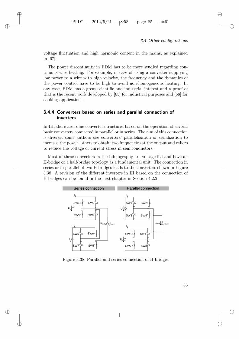
ii
“PhD” — 2012/5/21 — 8:58 — page 85 — #61 ii
ii
ii
3.4 Other configurations
voltage fluctuation and high harmonic content in the mains, as explainedin [67].
The power discontinuity in PDM has to be more studied regarding con-tinuous wire heating. For example, in case of using a converter supplyinglow power to a wire with high velocity, the frequency and the dynamics ofthe power control have to be high to avoid non-homogeneous heating. Inany case, PDM has a great scientific and industrial interest and a proof ofthat is the recent work developed by [65] for industrial purposes and [68] forcooking applications.
3.4.4 Converters based on series and parallel connection ofinverters
In IH, there are some converter structures based on the operation of severalbasic converters connected in parallel or in series. The aim of this connectionis diverse, some authors use converters’ parallelization or serialization toincrease the power, others to obtain two frequencies at the output and othersto reduce the voltage or current stress in semiconductors.
Most of these converters in the bibliography are voltage-fed and have anH-bridge or a half-bridge topology as a fundamental unit. The connection inseries or in parallel of two H-bridges leads to the converters shown in Figure3.38. A revision of the different inverters in IH based on the connection ofH-bridges can be found in the next chapter in Section 4.2.2.
Ue
Ie
Ue
Ieutank itank
Series connection Parallel connection
SW1
SW3
SW2
SW4
SW5 SW6
SW7 SW8
Ue
Ie
Ue
Ieutank itank
SW1
SW3
SW2
SW4
SW5 SW6
SW7 SW8
Figure 3.38: Parallel and series connection of H-bridges
85

Chapter 3 Induction heating converters
3.4.5 Special applications
IH is used in many different fields and a huge variety of solutions havebeen developed depending on the application. The quantity of convertertopologies and tanks found for these different applications, makes difficultto realize a complete review on them. In this study, just the most commonstructures used in continuous wire heating have been presented. However,there are many different topologies, tanks and control techniques that areused in other applications and that have not been explained. In this section,a selection of some interesting converters are introduced with the aim ofproviding a wider overview on IH field.
First, a case requiring multiple inverters with multiple inductors and asingle workpiece is presented. Afterwards, dual frequency converters usedfor heating non-uniform shape workpieces are introduced. Then, inverterswith multiple inductors used in cooking applications are briefly explained.Finally, a converter that allows the dynamic variation of frequency withoutdecreasing the current is shown.
Multiple inverters with multiple highly coupled inductors
In most IH applications the converter is usually connected to a unique tankheating a workpiece. However, there are some applications where there is aunique workpiece and there are several inductors fed by different converters.
An interesting application regarding these converter-inductor systems he-ating semiconductors wafers is found in [69] and [70]. In this application,the control of the temperature is critical to maintain an uniform heating andavoid mechanical stress in the wafers. The reason of using different coils isthat it allows passing different currents through them, permitting a bettercontrol of the temperature in the workpiece. In Figure 3.39, a simple schemeof the connections of these type of systems is shown.
In the case presented, the inductors are concentric and have high mutualcoupling. Under these circumstances, there is power recirculation betweencoils due to the coupling and it becomes difficult to control the currentindependently. To avoid a circulating power between coils and improve thecontrol of the currents, a control method based on current phase angle isused. This control method consists in synchronizing the currents insteadof voltage waveforms, as shown in Figure 3.39. By controlling the phase-shift of currents, their value can be increased or decreased properly, so thatthe control of temperature is improved compared to a control with voltagesynchronization.
86

ii
“PhD” — 2012/5/21 — 8:58 — page 87 — #62 ii
ii
ii
3.4 Other configurations
Ue1
Ie
SW1
SW3 SW4
SW2
Ue2
Ie
SW5
SW7 SW8
SW6
Workpiece
t
u1
u2
u1
u2
t
i1
i2
θvoltage
i1
i2
Inductor 1
Inductor 2
Inductor 1 Inductor 2
Workpiece
Figure 3.39: Parallel operation of two H-bridges with two highly coupledinductors heating a workpiece.
In case of wire heating, where inductors are not concentric and the tem-perature homogeneity during the processes is not so critical, this kind ofconsiderations are not usually taken into account.
Dual frequency converters
In case of non uniform shape pieces, as for example gears, the use of twofrequencies allows a more uniform and efficient heat treatment. Usually,this heat treatment is done with completely separate systems or with twoconverters and one coil. Another method presented in [71] is to use oneconverter and one coil but connecting capacitors and changing the resonantfrequency of the tank.
In [72] a unique converter using a unique coil with two resonant frequen-cies is presented. The tank has 4-elements and two resonant frequencies,which are the heating frequencies. The converter feeding this tank is anH-bridge using a traditional pulse-width modulation technique. In this case,the frequency of the modulating signal is the lower tank’s resonant frequencyand the frequency of the carrier is the higher resonant frequency. The bene-
87

Chapter 3 Induction heating converters
fits of this system, compared to the traditional ones, is that allows the useof one inductor and one converter, decreasing the cost and allowing bothfrequencies at the same time.
Inverters with multiple inductors
These converters are considered in this section because they are widely usedin IH. Contrarily to the parallel connection of converters for feeding highpower loads, these converters are suitable for light loads.
They consist on a unique converter, usually a half-bridge, feeding differentinductors. Induction cookers are the most representative application wherethese converters are used. In these cookers there can be a unique convertersupplying power to different burners. Some experiences regarding this kindof converters are explained in [73–76].
In the present study, as the application considered is related to industrialwire heating treatments, where loads usually require much power, these typeof structures are not applicable.
Dynamic variable frequency converter
In case of a converter used for different heat treatments requiring differentfrequencies, it is necessary to vary the resonant frequency of the tank andadapt it to the new frequency. Otherwise, if the resonant frequency of thetank is not changed and the commutating frequency is the new one, thecurrent in the inductor is low and heat would not be generated. Usually,this change of resonant frequency is done manually by means of a change inthe capacitance of the resonant tank.
In [77] and [78] a converter that allows a dynamic variation of the fre-quency while maintaining the current in the inductor is presented. Themain advantage of this converter, compared to the traditional ones, is thatallows the variation of frequency while the current in the inductor is stillhigh and with no changes in hardware. A scheme of this type of converter isshown in Figure 3.40. It can be observed that it is a current-fed converter,but it has the resonant capacitor connected to the DC-bus. It has to benoted that one of the main drawbacks of this structure is that the currentin the load is also conducting in semiconductors. However, this converteris interesting because provides the opportunity of realizing heat treatmentswith a dynamic variation of the frequency.
88
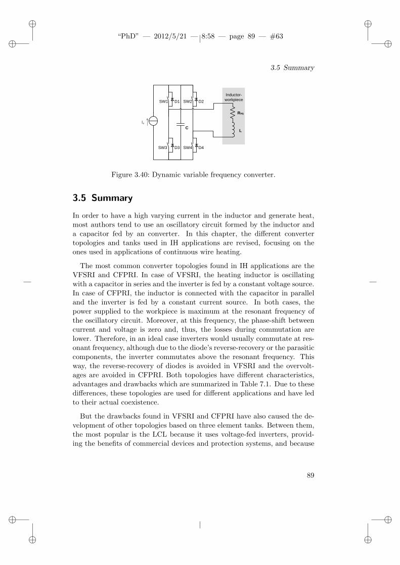
ii
“PhD” — 2012/5/21 — 8:58 — page 89 — #63 ii
ii
ii
3.5 Summary
Req
L
Inductor-workpiece
SW3 SW4
SW2D1
D3
D2
D4
SW1
IeC
Figure 3.40: Dynamic variable frequency converter.
3.5 Summary
In order to have a high varying current in the inductor and generate heat,most authors tend to use an oscillatory circuit formed by the inductor anda capacitor fed by an converter. In this chapter, the different convertertopologies and tanks used in IH applications are revised, focusing on theones used in applications of continuous wire heating.
The most common converter topologies found in IH applications are theVFSRI and CFPRI. In case of VFSRI, the heating inductor is oscillatingwith a capacitor in series and the inverter is fed by a constant voltage source.In case of CFPRI, the inductor is connected with the capacitor in paralleland the inverter is fed by a constant current source. In both cases, thepower supplied to the workpiece is maximum at the resonant frequency ofthe oscillatory circuit. Moreover, at this frequency, the phase-shift betweencurrent and voltage is zero and, thus, the losses during commutation arelower. Therefore, in an ideal case inverters would usually commutate at res-onant frequency, although due to the diode’s reverse-recovery or the parasiticcomponents, the inverter commutates above the resonant frequency. Thisway, the reverse-recovery of diodes is avoided in VFSRI and the overvolt-ages are avoided in CFPRI. Both topologies have different characteristics,advantages and drawbacks which are summarized in Table 7.1. Due to thesedifferences, these topologies are used for different applications and have ledto their actual coexistence.
But the drawbacks found in VFSRI and CFPRI have also caused the de-velopment of other topologies based on three element tanks. Between them,the most popular is the LCL because it uses voltage-fed inverters, provid-ing the benefits of commercial devices and protection systems, and because
89

Chapter 3 Induction heating converters
the current in semiconductors is lower than in the inductor. However, thisstructure also have some drawbacks, like the need of high Q values to avoidhigh reactive power or the need of an additional inductance. These draw-backs have limited their application to certain cases with high Q values, likehigh-frequency heating treatments.
Table 3.1: Comparison between VFSRI and CFPRI.
VFSRI CFPRI
The inverter is fed by a capacitor thatmaintains the voltage.
The inverter is fed by an inductancethat maintains the current.
Dead-time between switches is re-quired to avoid short-circuit.
Ovelap time is required to avoid over-voltage.
Needs short circuit protection. Has inherent short-circuit capability.
In case of failure all the switches haveto be turned-off.
In case of failure all the switches haveto be turned-on.
Voltage-fed converters are easily foundin medium power applications. Com-mercial protection circuits can be usedin case of short-circuit.
Current-fed converters are usuallyfound for high power applications (>1 MW). Special protection circuits anddrivers are needed in case of overvolt-age.
The voltage feeding the tank is asquare wave and the current is sinu-soidal.
The current feeding the tank is asquare wave and the voltage is sinu-soidal.
The voltage on the inductor is Q timeshigher than at the output of the con-verter, but the current in the tank isthe same than in the inductor. Usu-ally a matching transformer is neededbetween the inverter and the tank.
The current in the inductor is approx-imately Q times the current at theoutput of the converter. A matchingtransformer is not usually required.
High voltage capacitors are sometimesneeded for the tank.
High voltage capacitors are not re-quired but more capacitors in parallelare needed.
Switches of the inverter have to be uni-directional in voltage but bidirectionalin current. The antiparallel-diode isnecessary.
Switches have to be unidirectional incurrent but bidirectional in voltage. Aseries diode is needed.
The converter is switching at inductiveswitching ( fsw > fr).
The converter is switching at capaci-tive switching ( fsw > fphase0).
Another important element that has solved some of the drawbacks ofVFSRI and CFPRI is the matching transformer. These transformers haveallowed the widespread of VFSRI by reducing the current in semiconductors,
90

ii
“PhD” — 2012/5/21 — 8:58 — page 91 — #64 ii
ii
ii
3.5 Summary
but they are also used in many applications with different topologies. Theycan be classified as active power transformers and reactive power transform-ers.
Regarding the manner of controlling the power supplied to the workpiece,there are different control techniques. One is by commutating the inverterwith a 50 % of duty-cycle and controlling the input DC source. In this case,the commutation losses of the inverter are low. However, this DC sourceis obtained from a thyristor bridge rectifier, increasing the cost and size, orwith a DC/DC converter like a buck, which decreases the efficiency of theoverall system.
There are other power control techniques that use uncontrolled rectifier,which reduces the cost and complexity of the converter. These techniques arebased on controlling the power by varying the inverter’s frequency or varyingthe pulse width. The problems found when using these techniques are theincrease of the reactive power supplied by the inverter and the increase ofcommutation losses. In order to solve these problems but maintain thestructure based on an uncontrolled rectifier, PDM techniques have aroused.These techniques are based on the control of the power through the numberof pulses supplied to the load, while the inverter is commutating at 50 % ofduty-cycle and close to the resonant frequency, thus, decreasing the losses.It has also some drawbacks, like the discontinuity of the power levels or thedifficulty to calculate this power at low power levels.
Another important type of converters explained in this chapter are thosebased on the serialization and parallelization of basic inverters like H-bridges.The aim of serializing basic inverters is to reduce voltage stress in semicon-ductors and, for example, use MOSFETs in high voltage applications. Thereare also authors that use this connection for obtaining more frequency atthe output. In case of parallelization, the aim is to obtain higher power atthe output, but also increasing the frequency at the output which allows,for example, the use of IGBTs in high frequency applications.
In this chapter, the most common topologies, tanks and considerationsregarding converters used in wire heating are described. At the end, somespecial applications are described to provide a wider overview on IH convert-ers. This chapter introduces the concepts used during the work developedin next chapters. Moreover, allows to understand converters’ performance,limitations and considerations depending on the structure and the controlchosen, that leads to the conclusion that there is not a unique and perfectconverter. Every structure has its advantages and limitations, being use-
91

Chapter 3 Induction heating converters
ful depending on the application or circumstances and requiring a specificanalysis for each application.
92

ii
“PhD” — 2012/5/21 — 8:58 — page 93 — #65 ii
ii
ii
Chapter 4
Study of a multichannel converter forhigh-power high-frequencyapplications
4.1 Introduction
There are many converter topologies and resonant tanks used in IH appli-cations. With regard to this variety, there are converters based on paralleland series connection of basic topologies. The aim of these connections isdiverse, being one of them the creation of a basic structure that allows toreach any power at any frequency when implemented repeatedly.
The idea of a converter based on paralleling and serializing basic converterstructures is extremely interesting for IH industry. This modularity canproduce benefits in terms of maintenance and rapid repairing, which resultsin increasing the reliability of system. Moreover, in case of failure and witha critical industrial process, these types of structures can allow maintainingthe process at half of the power while waiting for a spare part to solve thefailure.
In this chapter, this modularity idea is studied for high-power and high-frequency IH converters, in particular for converters in the range of 50 to 500kVA and 50 to 300 kHz. First, in Section 4.2, the multichannel converter isstudied for defining its basic structure. Afterwards, in Section 4.3, a multi-channel converter is implemented and finally, in Section 4.4, this chapter issummarized.
93

Chapter 4 Study of a multichannel converter
4.2 Design of a multichannel converter for inductionheating
The underlying idea of the multichannel converter applied to IH field, is thecreation of basic hardware structures that are connected in series or parallelto fulfill the converter’s specifications. A basic scheme of this concept, whichis somehow related to the power electronic building block concept explainedin [79], is shown in Figure 4.1. The benefits of this design procedure arethe reduction in cost due to a higher volume production, the reduction ofengineering effort and time, the reduction of design testing and the reductionof installation and maintenance work.
The principal analysis of the study realized in this chapter is based on theinverter stage and the connection of inverters to form a multichannel con-verter. First, in Section 4.2.1, some considerations regarding the topologyand the semiconductors are given to define the basic structures composingthe multichannel converter. Afterwards, in Section 4.2.2, the different in-verter topologies based on series and parallel connection of H-bridges arerevised. The different connections of H-bridges are studied for the case ofthe multichannel converter in Section 4.2.3 and, finally, the multichannelconverter structure is presented in Section 4.2.4.
AC/DC AC/DC
Resonanttank
AC/DC AC/DCAC/DC AC/DC
AC/DC AC/DCAC/DC DC/AC
Converter
Mains
Figure 4.1: Multichannel converter basic scheme.
4.2.1 Preliminary considerations
When considering a converter based on the connection of basic structures,the first step is to define these basic structures. In order to reduce thenumber of components, it is interesting to eliminate the power control stagebetween the mains and the inverter, using one of the techniques presentedin Section 3.4.3. Taking this into consideration, the AC/DC conversion canbe realized with an uncontrolled diode bridge rectifier. With regard to the
94

ii
“PhD” — 2012/5/21 — 8:58 — page 95 — #66 ii
ii
ii
4.2 Design of a multichannel converter for induction heating
DC/AC stage, the basic inverter topology used in applications above fewkVA is the H-bridge, as shown in Chapter 3.
Concerning the feeding of the H-bridge, there are two possibilities: cur-rent and voltage-feeding. In case of a CFPRI, it is possible to increase thepower by parallelization. In case of needing an increase of frequency, it ispossible to interleave two CFPRI with the output in series. In this case,when one converter is conducting, the other has to be short-circuited. It hasto be noted that the use of CFPRI leads to the need of specific drivers andovervoltage protection systems, explained in Section 3.3.5.
In case of VFSRI, commercial devices like drives or power modules withdrivers incorporated can be used, benefitting from all the advantages ofreliability, flexibility and price reduction. The use of commercial devices isin consonance with the aim of profiting higher volume productions.
With regard to the type of semiconductors used in the H-bridge, IGBTsand MOSFETs are the most commonly used devices in this range of fre-quency and power. Considering MOSFETs, the main limitation is the max-imum power provided by these devices. If a structure without intermediatepower control stage is used, the semiconductors have to support at least 800V because the voltage at the DC bus is 560 V (400 V rectified from themains).
In case of commercial MOSFETs, as their voltage breakdown increases,the current they can support decreases rapidly. Usually, MOSFETs withbreakdown voltages above 600 V cannot conduct more than 60 A at 85 oC.Moreover, these devices tend to use TO-220, SOT-227 or similar packages,that are more fragile and problematic to manipulate than modules. In addi-tion to these limitations, there are problems derived from using MOSFETsin VFSRIs due to the unwanted turn-on of their parasitic BJTs, as explainedin Section 3.2.5. Nevertheless, it has to be noted that new advances in MOS-FETs and the addition of antiparallel FREDFET diodes have substantiallyreduced this problem.
The problem derived from the use of low power devices can be solvedemploying high-voltage MOSFETs in parallel or low-voltage MOSFETs inseries, but a lot of devices are needed and the cost increases considerably.
The improvement during last years in IGBTs’ technology, by reducingthe turn-off losses as well as their conduction losses, shown in [80] and [81],make them nowadays a good alternative for IH applications. They allowa higher power density of the converter and, with the appearance of the
95

Chapter 4 Study of a multichannel converter
Non Punch-Through IGBTs, its parallelization permits increasing the finalpower up to very high values. This allows a basic structure with fewercomponents than in case of using MOSFETs. Moreover, power IGBTs areusually encapsulated with modules like D61 or D56, which are better tomanipulate, increasing the robustness of the converter.
In any case, it has to be noted that IGBT devices are not exempt ofproblems and, at the moment, there are some MOSFET manufacturers withcommercial 1000 V, 100 A devices with SiC antiparallel diodes and SP6packages. However, these types of devices are not so common and are moreexpensive. Therefore, the best choice for the moment is an IGBT-basedH-bridge that improves IH converters’ performance, volume and cost in thisrange of power and frequencies.
Considering the comments realized during this section, the converter isformed by two basic structures: a three phases diode rectifier and a voltage-fed H-bridge, as shown in Figure 4.2. With regard to the diode bridgerectifier, this part does not pose much design difficulties, therefore, the fol-lowing sections are focused mainly in the connection of H-bridge inverters.It has to be noted that in case of high power converters, the diodes canbe paralleled and, in case of power values above hundreds of kVA, 12 pulsebridge rectifiers can be used.
Figure 4.2: Multichannel converter basic configuration.
4.2.2 Revision of inverters based on series and parallelconnection of H-bridges
In IH literature, there are several authors using inverter structures basedon the parallel or series connection of H-bridges. Some authors use thisconnection to increase the power, to obtain two frequencies at the output orto reduce the voltage or current stress in semiconductors.
96

ii
“PhD” — 2012/5/21 — 8:58 — page 97 — #67 ii
ii
ii
4.2 Design of a multichannel converter for induction heating
In this section, the inverters based on H-bridges series connection areexplained first and, afterwards, the inverters based on parallel connection.
Inverters based on series connection of H-bridges
The series connection of H-bridges shown in Figure 4.3 is identical to thetopology used in multilevel inverters, specifically known as cascade half-bridge multilevel inverter [82, p. 51]. These types of inverters have beendesigned to lower the voltage stress in semiconductors for the case of high-voltage applications. The benefits are the use of low-voltage semiconductorswith better characteristics and the decrease in the output’s harmonic contentby using more than two voltage-levels. At this moment, multilevel convertersare widely used in high power applications like mining, navy or railways, butthey are gaining importance in renewable energies and other fields. In fact,semiconductor manufacturers have packs including these topologies for awide power range.
Ue
Ie
SW1
SW3 SW4
SW2
Ue
Ie
SW5
SW7 SW8
SW6
utankitank
Figure 4.3: Two H-bridge structures connected in series.
In case of IH, some authors like [83] use this topology to reduce the voltagestress in semiconductors. This reduction in voltage stress allows the use ofMOSFETs in higher voltage applications and, thus, the construction of highvoltage and high frequency converters.
97
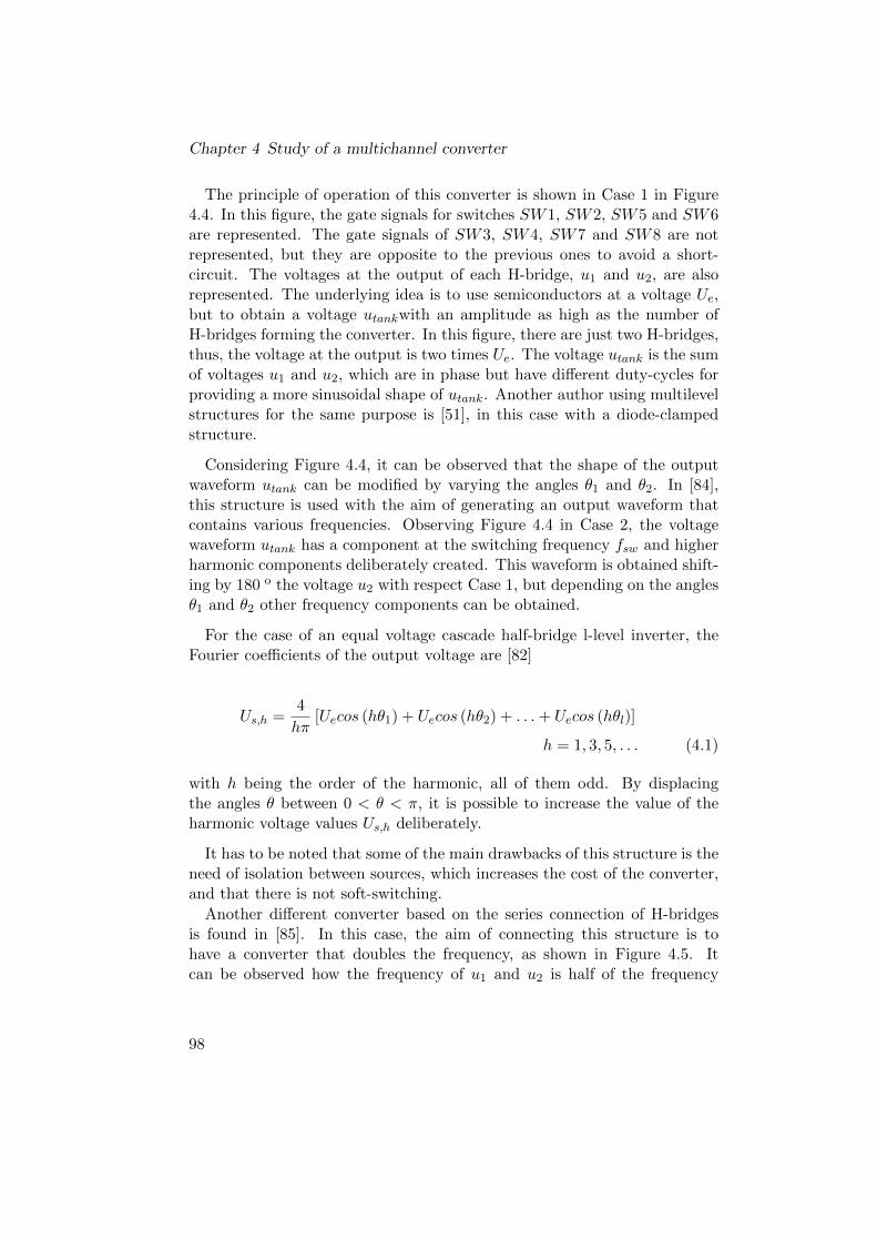
Chapter 4 Study of a multichannel converter
The principle of operation of this converter is shown in Case 1 in Figure4.4. In this figure, the gate signals for switches SW1, SW2, SW5 and SW6are represented. The gate signals of SW3, SW4, SW7 and SW8 are notrepresented, but they are opposite to the previous ones to avoid a short-circuit. The voltages at the output of each H-bridge, u1 and u2, are alsorepresented. The underlying idea is to use semiconductors at a voltage Ue,but to obtain a voltage utankwith an amplitude as high as the number ofH-bridges forming the converter. In this figure, there are just two H-bridges,thus, the voltage at the output is two times Ue. The voltage utank is the sumof voltages u1 and u2, which are in phase but have different duty-cycles forproviding a more sinusoidal shape of utank. Another author using multilevelstructures for the same purpose is [51], in this case with a diode-clampedstructure.
Considering Figure 4.4, it can be observed that the shape of the outputwaveform utank can be modified by varying the angles θ1 and θ2. In [84],this structure is used with the aim of generating an output waveform thatcontains various frequencies. Observing Figure 4.4 in Case 2, the voltagewaveform utank has a component at the switching frequency fsw and higherharmonic components deliberately created. This waveform is obtained shift-ing by 180 o the voltage u2 with respect Case 1, but depending on the anglesθ1 and θ2 other frequency components can be obtained.
For the case of an equal voltage cascade half-bridge l-level inverter, theFourier coefficients of the output voltage are [82]
Us,h =4
hπ[Uecos (hθ1) + Uecos (hθ2) + . . .+ Uecos (hθl)]
h = 1, 3, 5, . . . (4.1)
with h being the order of the harmonic, all of them odd. By displacingthe angles θ between 0 < θ < π, it is possible to increase the value of theharmonic voltage values Us,h deliberately.
It has to be noted that some of the main drawbacks of this structure is theneed of isolation between sources, which increases the cost of the converter,and that there is not soft-switching.
Another different converter based on the series connection of H-bridgesis found in [85]. In this case, the aim of connecting this structure is tohave a converter that doubles the frequency, as shown in Figure 4.5. Itcan be observed how the frequency of u1 and u2 is half of the frequency
98
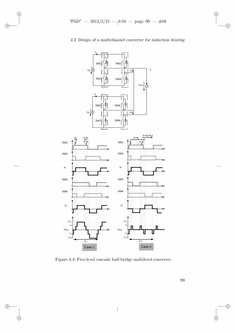
ii
“PhD” — 2012/5/21 — 8:58 — page 99 — #68 ii
ii
ii
4.2 Design of a multichannel converter for induction heating
Ue
Ie
t
t
t
SW6
SW1
SW3 SW4
SW2
2·Ue
Ue
t
SW1
Ue
Ie
SW5
SW7 SW8
SW6
is
SW2
t
SW5
-2·Ue
-Ue
1/fsw
θ1
θ2
Case 1
u1
u2
u1
t
t
u2
t
t
t
SW6
2·Ue
Ue
t
SW1
SW2
t
SW5
-2·Ue
-Ue
1/fsw
π+θ2
Case 2
u1
t
t
u2
π-θ1
π+(π-θ2)
utank
utank
π-θ1
π-θ2
θ1
utank
Figure 4.4: Five-level cascade half-bridge multilevel converter.
99
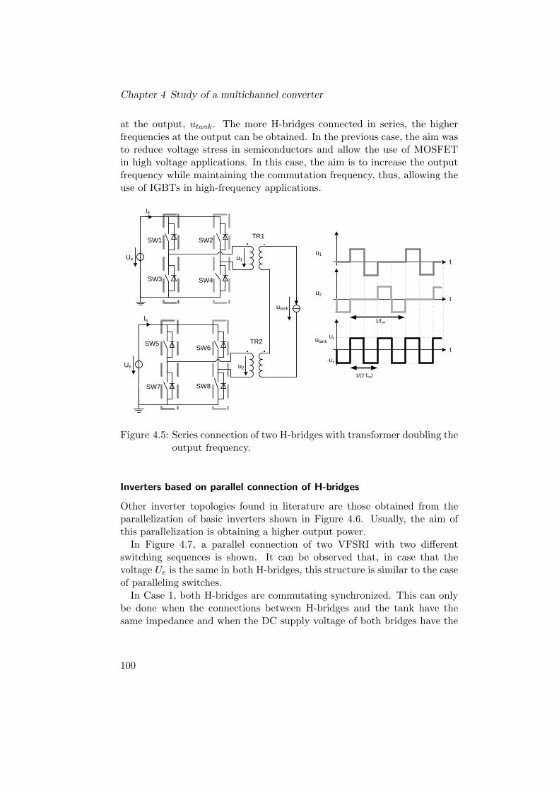
Chapter 4 Study of a multichannel converter
at the output, utank. The more H-bridges connected in series, the higherfrequencies at the output can be obtained. In the previous case, the aim wasto reduce voltage stress in semiconductors and allow the use of MOSFETin high voltage applications. In this case, the aim is to increase the outputfrequency while maintaining the commutation frequency, thus, allowing theuse of IGBTs in high-frequency applications.
Ue
Ie
SW1
SW3 SW4
SW2
Ue
Ie
SW7 SW8
SW6
TR1
TR2
u1
u2
t
Ue
-Ue
t
u1
1/(2·fsw)
1/fsw
tu2
SW5
utank
utank
Figure 4.5: Series connection of two H-bridges with transformer doubling theoutput frequency.
Inverters based on parallel connection of H-bridges
Other inverter topologies found in literature are those obtained from theparallelization of basic inverters shown in Figure 4.6. Usually, the aim ofthis parallelization is obtaining a higher output power.
In Figure 4.7, a parallel connection of two VFSRI with two differentswitching sequences is shown. It can be observed that, in case that thevoltage Ue is the same in both H-bridges, this structure is similar to the caseof paralleling switches.
In Case 1, both H-bridges are commutating synchronized. This can onlybe done when the connections between H-bridges and the tank have thesame impedance and when the DC supply voltage of both bridges have the
100

ii
“PhD” — 2012/5/21 — 8:58 — page 101 — #69 ii
ii
ii
4.2 Design of a multichannel converter for induction heating
Ue
Ie
SW1
SW3 SW4
SW2
Ue
Ie
SW5
SW7 SW8
SW6
utankitank
Figure 4.6: Two H-bridge structures connected in parallel.
same value. This operation is similar to paralleling semiconductors, whichis a connection used in many applications to increase the power.
Other possibility is to commutate the H-bridges alternatively at half of thefrequency, as shown in Figure 4.7 in Case 2. In this case, the frequency ofthe output waveform utank is twice the commutation frequency, which allowsthe use of IGBTs in high frequency applications. This case is similar to thecase shown in Figure 4.5 for the series connection. The difference is that allswitches of one H-bridge have to be blocked while the other is commutating,whereas in the previous case, two switches need to be conducting while theother H-bridge is commutating.
In [53, 86, 87], this parallelization is used commutating as in Case 2 inFigure 4.7. In [53] and [86], the benefits of this commutation techniqueare compared to the benefits of commutating as in Case 1 in Figure 4.7 toreach higher frequencies. The underlying idea is the proportional decreaseof IGBT losses at high currents. In Case 1, switches’ current has an ampli-tude half of the output current’s amplitude. Thus, switches are destressedbecause the current level is lower and the commutation frequency can behigher. In case 2, the current is also half of the output current becauseswitches conduct half of the period, but the peak current is the same thanthe output’s current. Considering that VFSRI commutate with inductive
101
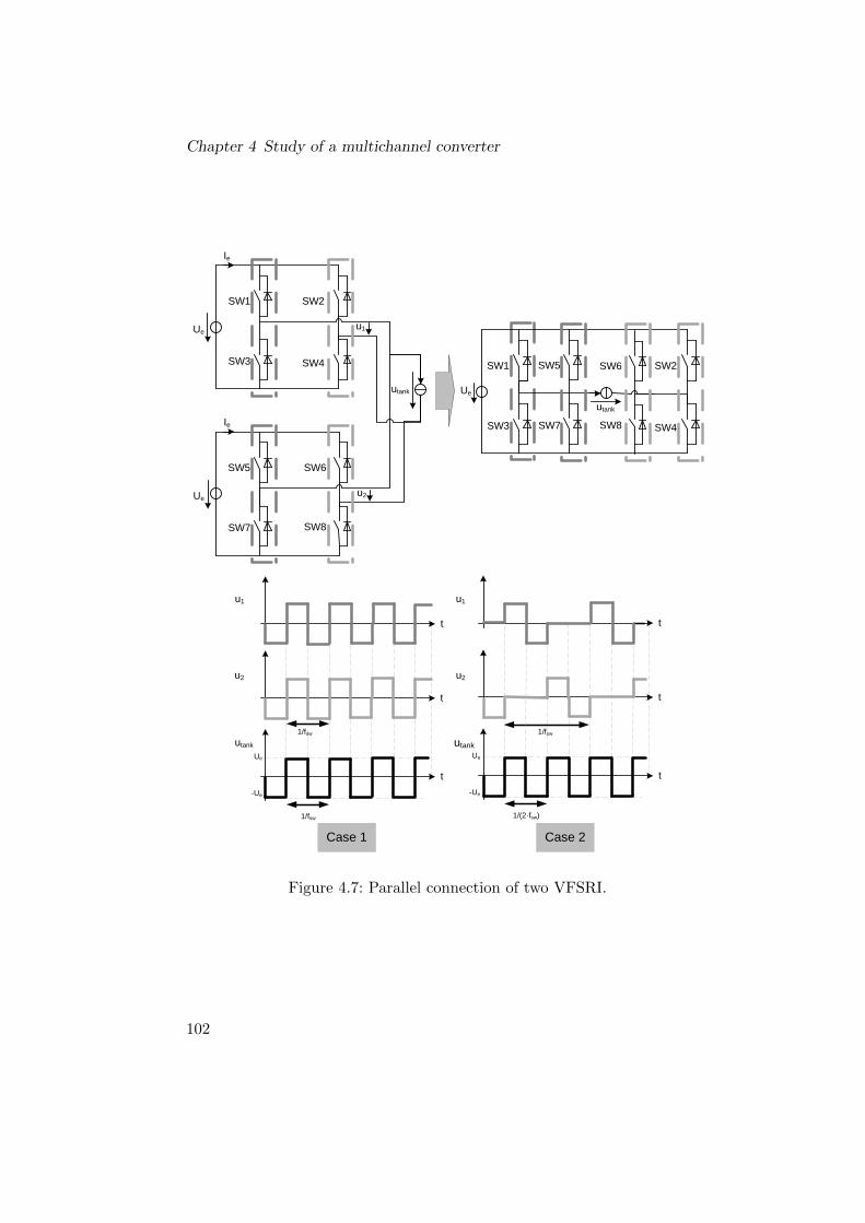
Chapter 4 Study of a multichannel converter
Ue
Ie
SW1
SW3 SW4
SW2
Ue
Ie
SW5
SW7 SW8
SW6
Ue
SW1
SW3 SW4
SW2
utank
SW5
SW7 SW8
SW6
u1
u2
t
utankUe
-Ue
t
u1
1/(2·fsw)
1/fsw
t
u2
t
Ue
-Ue
t
u1
1/fsw
t
u2
utank
Case 1 Case 2
1/fsw
utank
Figure 4.7: Parallel connection of two VFSRI.
102

ii
“PhD” — 2012/5/21 — 8:58 — page 103 — #70 ii
ii
ii
4.2 Design of a multichannel converter for induction heating
switching, commutation losses occur during the transistors’ turn-off. In caseof IGBTs, this energy-loss is proportionally lower in case of high currentsthan in low currents. Although the conduction losses increase because thereare higher currents during less time, the overall losses per semiconductorare lower. Therefore, commutating as in Case 2 improves converter’s perfor-mance. In any case, it has to be noted that obtaining a realistic value frommanufacturers’ datasheets for comparing both strategies is difficult and hasto be particularized.
Other authors using parallelization of converters with LCL tanks can befound in [45] and [46]. In this case, authors take advantage of the inductanceat the output of the inverters, which allows an easy connection betweeninverters and avoids any recirculation. The aim of this parallelization is toincrease the total output power. In Figure 4.8 this connection is shown andit can be observed that the commutation process is equal to Case 1 in Figure4.7.
t
utank
Ue
-Ue
t
u1
1/fsw
t
u2
Ue
Ie
SW1
SW3 SW4
SW2
Ue
Ie
SW5
SW7 SW8
SW6
u1
u2
utank
1/fsw
Figure 4.8: Parallel connection of two H-bridges with LCL tank to increaseoutput power.
103

Chapter 4 Study of a multichannel converter
4.2.3 Analysis of H-bridge inverters connection for themultichannel converter
In the previous section, the different topologies of IH converters based onserialization and parallelization of H-bridge inverters are overviewed. Inthis section, the same structures with different types of commutations areexposed and the advantages and drawbacks of each one for its use in amultichannel converter are explained.
First, the H-bridge converter with its commutation states and commuta-tion techniques is explained with the aim of providing a better understandingof the following analysis. Afterwards, the series and the parallel connectionof H-bridges is discussed for the case of a multichannel converter.
H-bridge structure analysis
In Figure 4.9, a voltage-fed H-bridge structure is shown. Considering thattwo switches of the same inverter leg cannot commutate at the same time,it can be assumed that the state of the switches (ON and OFF) of the sameinverter leg are contrary. Thus, there are four possible states in an H-bridge,as shown in Table 4.1.
Ue
Ie
SW1
SW3 SW4
SW2
utank
itank
Figure 4.9: H-bridge structure.
In Figure 4.10, three possible commutation methods to obtain an AC volt-age at the output of the H-bridge are shown. In Case 1, SW1 and SW2 havea duty-cycle d of 50 % and commutate shifted 180 o. The resulting wave-form is a square wave of ±Ue and frequency fsw, being fsw the commutationfrequency.
104

ii
“PhD” — 2012/5/21 — 8:58 — page 105 — #71 ii
ii
ii
4.2 Design of a multichannel converter for induction heating
Ue
Ie t
SW1
t
t
utank
SW2
SW1
SW3 SW4
SW2
Ue
-Ue
1/fsw
d = 0.5 d
SW1SW4
SW3SW2
Commutation State
II III
SW1SW4
SW3SW2
II III
1/fsw
On switches
ᶲ = 180º ᶲ =180º
utank
itank
Case 1
t
SW2
t
utank
Ue
-Ue
t
SW1
1/fsw
SW1SW4
SW3SW2
Commutation State
II III
SW3SW4
IV
SW1SW2
I
SW1SW4
SW3SW2
II III
SW3SW4
IV
SW1SW2
I
Ue
Ie
SW1
SW3 SW4
SW2
d = 0.5 dᶲ
utank
itank
ᶲ
On switches
1/fsw
Case 2
Ue
Ie
SW1
SW3 SW4
SW2
d = 0.75 (1-d)ᶲ = 90º
utank
itank
Case 3
t
t
t
utank
Ue
-Ue
SW1SW4
II
SW1SW2
I
SW1SW4
II
SW3SW4
IV
SW1SW4
II
SW1SW2
I
SW1SW4
II
SW3SW4
IV
SW2
SW1
1/fsw
1/2fsw
Commutation State
On switchesSW1SW4
I
ᶲ = 90º
Figure 4.10: Commutation techniques for an H-bridge structure.
105

Chapter 4 Study of a multichannel converter
Table 4.1: Commutation states for an H-bridge
State SW1 SW2 utank
I ON ON 0II ON OFF UeIII OFF ON −UeIV OFF OFF 0
In Case 2, the duty-cycle is maintained for the two inverter legs, but thephase-shift φ is not 180 o. Under these circumstances, the commutationstates are States IV-II-I-III and the output waveform is the same than inCase 1, but with zero voltage at States I and IV. In this case, the com-mutation occurs when the current is not zero and the commutation lossesincrease.
In the last case, Case 3, the duty-cycles are 75 % and 25 % and theirphase-shift is 90o. Under these circumstances, the resulting output waveformdoubles the frequency of commutation. However, the voltage is just positiveand the first harmonic voltage value in RMS is [88]
Utank =2Ue√
2π(4.2)
which is half of the value obtained with a ±Ue waveform, as shown in Equa-tion 7.1 in Section 3.2.2. Thus, the frequency is increased, but the powersupplied to the workpiece is a quarter of the power supplied when commu-tating as in Case 1 (Equation 3.20 in Section 3.2.3). Moreover, this commu-tation method cannot be used in case of having a matching transformer dueto its saturation.
Two H-bridge structures connected in series
In Figure 4.3, the series connection of two H-bridges is shown. In this case, ithas to be assumed that both voltage sources are isolated. As in the previouscase, it is considered that the switches from the same inverter leg commutatecontrarily. The commutation states for this connection are defined in Table4.2.
In the series connection of H-bridges, there are also several commutationtechniques that lead to different output waveforms. In Figure 4.11, 4.12 and4.13 five different cases are presented.
106

ii
“PhD” — 2012/5/21 — 8:58 — page 107 — #72 ii
ii
ii
4.2 Design of a multichannel converter for induction heating
Table 4.2: Commutation states of two H-bridge structures in series.
State SW1 SW2 SW5 SW6 utank
I ON ON ON ON 0II ON ON ON OFF UeIII ON ON OFF ON −UeIV ON ON OFF OFF 0V ON OFF ON ON UeVI ON OFF ON OFF 2UeVII ON OFF OFF ON 0VIII ON OFF OFF OFF UeIX OFF ON ON ON −UeX OFF ON ON OFF 0XI OFF ON OFF ON −2UeXII OFF ON OFF OFF −UeXIII OFF OFF ON ON 0XIV OFF OFF ON OFF UeXV OFF OFF OFF ON −UeXVI OFF OFF OFF OFF 0
In Case 1 in Figure 4.11 , both H-bridges commutate synchronized, theduty-cycle of SW1 and SW5 is 50 % and the phase-shift φ1 and φ2 are 180o.The resulting waveform has a ±2Ue voltage amplitude at a fsw frequency.This case is similar to Case 1 in Figure 4.10 for one H-bridge.
In Case 2, all switches have a 75 % of duty-cycle, SW5 is delayed 180o
from SW1 (φ12 = 180o) and SW2 and SW6 are delayed 90o regarding theiropposite switches, SW1 and SW5 respectively. In this case, the resultingoutput waveform has doubled the frequency of commutation, but has half ofthe voltage than in the previous case. Case 3 is similar, but the dead-timesare different, as shown in Figure 4.12.
Case 4 in Figure 4.13 can be used in case of needing a higher output voltagewith higher frequency. In this case, SW1 and SW5 are synchronous and havea duty-cycle of 75 %. SW2 and SW6 have a 25 % of duty-cycle and theyare delayed 90o regarding their opposite switches SW1 and SW5. Underthese circumstances, the resulting waveform has doubled the frequency andhas an amplitude of 2Ue V. The problem of this commutation technique isthat a matching transformer cannot be used. The same happens in Case 5in Figure 4.13, where the output waveform has quadrupled the frequency,
107
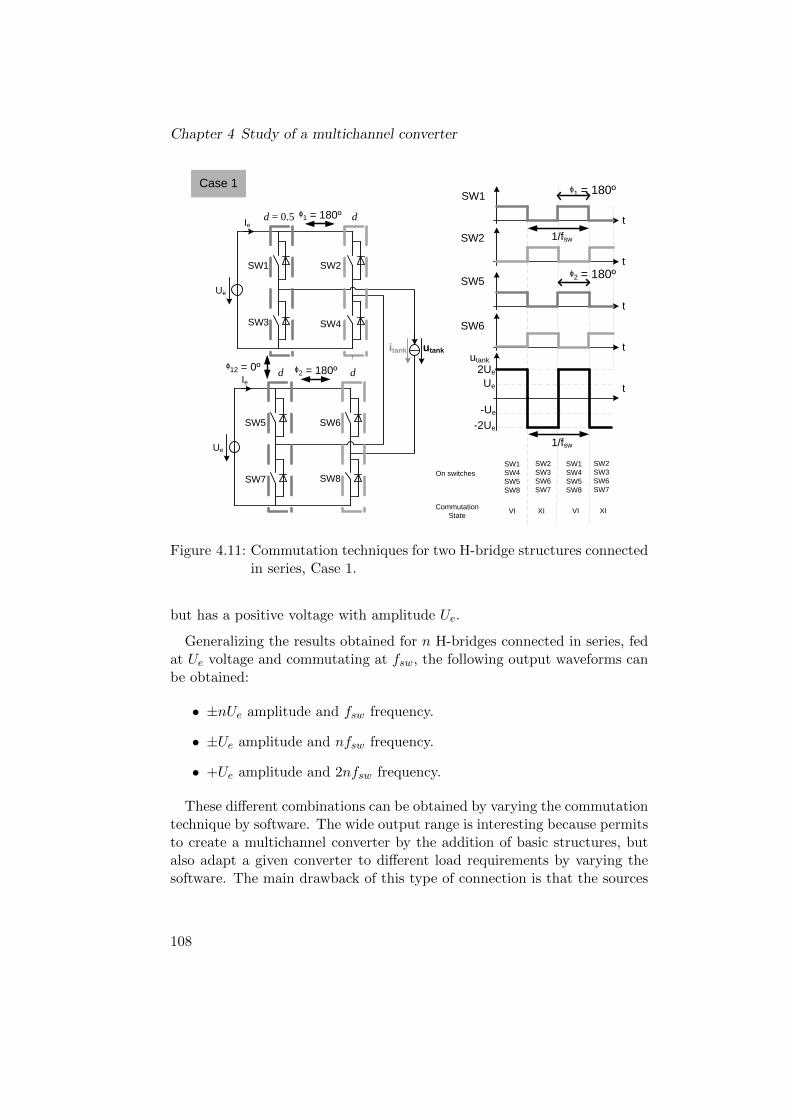
Chapter 4 Study of a multichannel converter
Ue
Ie
t
t
t
utank
SW6
SW1
SW3 SW4
SW2
Ue
-Ue
t
SW1
1/fsw
1/fsw
Ue
Ie
SW5
SW7 SW8
SW6
SW2
t
SW5
SW1SW4SW5SW8
SW2SW3SW6SW7
VI XI
2Ue
SW1SW4SW5SW8
SW2SW3SW6SW7
VI XI
Case 1
d = 0.5 d
d d
utankitank
Commutation State
On switches
ᶲ1 = 180º
ᶲ1 = 180º
ᶲ2 = 180º
ᶲ2 = 180ºᶲ12 = 0º
-2Ue
Figure 4.11: Commutation techniques for two H-bridge structures connectedin series, Case 1.
but has a positive voltage with amplitude Ue.
Generalizing the results obtained for n H-bridges connected in series, fedat Ue voltage and commutating at fsw, the following output waveforms canbe obtained:
• ±nUe amplitude and fsw frequency.
• ±Ue amplitude and nfsw frequency.
• +Ue amplitude and 2nfsw frequency.
These different combinations can be obtained by varying the commutationtechnique by software. The wide output range is interesting because permitsto create a multichannel converter by the addition of basic structures, butalso adapt a given converter to different load requirements by varying thesoftware. The main drawback of this type of connection is that the sources
108

ii
“PhD” — 2012/5/21 — 8:58 — page 109 — #73 ii
ii
ii
4.2 Design of a multichannel converter for induction heating
t
t
t
utank
SW6
Ue
-Ue
t
SW1
SW1SW2SW7SW6
SW2
t
SW5
SW1SW4SW5SW6
SW3SW4SW7SW6
SW1SW4SW7SW8
III V XV VIII
SW1SW2SW7SW6
SW1SW4SW5SW6
SW3SW4SW7SW6
SW1SW4SW7SW8
III V XV VIII
Ue
Ie
SW1
SW3 SW4
SW2
Ue
Ie
SW5
SW7 SW8
SW6
Case 3
d = 0.75 (1-d)
(1-d) d
utankitank
ᶲ1 = 90º
ᶲ2 = 90º
Commutation State
On switches
ᶲ1 = 90º
1/fsw
ᶲ12 = 180º
ᶲ2 = 90º
ᶲ12 = 180º
1/2fsw
Ue
Ie
SW1
SW3 SW4
SW2
Ue
Ie
SW5
SW7 SW8
SW6
Case 2
d = 0.75 d
d d
utankitank
Commutation State
On switches
ᶲ1 = 90º
ᶲ2 = 90º
t
t
t
utank
SW6
Ue
-Ue
t
SW1
SW1SW2SW7SW6
SW2
t
SW5
SW1SW2SW5SW8
SW3SW2SW5SW6
III II IX
SW1SW4SW5SW6
V
SW1SW2SW7SW6
SW1SW2SW5SW8
SW3SW2SW5SW6
III II IX
SW1SW4SW5SW6
V
1/fsw
ᶲ1 = 90º
ᶲ12 = 180º
ᶲ2 = 90º
ᶲ12 =180º
1/2fsw
Figure 4.12: Commutation techniques for two H-bridge structures connectedin series, Cases 2 and 3.
109
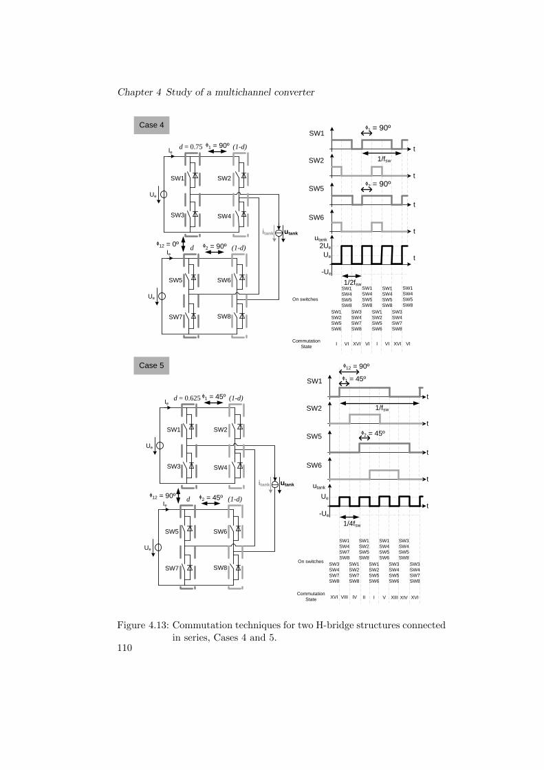
Chapter 4 Study of a multichannel converter
Ue
Ie
SW1
SW3 SW4
SW2
Ue
Ie
SW5
SW7 SW8
SW6
Case 5
d = 0.625 (1-d)
d (1-d)
utankitank
ᶲ1 = 45º
ᶲ2 = 45º
Commutation State
On switches
ᶲ12 = 90º
ᶲ1 = 45º
ᶲ12 = 90º
utank
SW6
Ue
-Ue
SW1
SW3SW4SW7SW8
SW2
SW5
SW1SW4SW7SW8
SW1SW2SW7SW8
XVI VIII IV
SW1SW2SW5SW8
II
SW1SW2SW5SW6
SW1SW4SW5SW6
SW3SW4SW5SW6
I V XIII
SW3SW4SW5SW8
XIV
SW3SW4SW7SW8
XVI
1/fsw
t
t
t
t
t
ᶲ2 = 45º
1/4fsw
Ue
Ie
t
t
t
utank
SW6
SW1
SW3 SW4
SW2
Ue
-Ue
t
SW1
1/2fsw
SW1SW2SW5SW6
1/fsw
Ue
Ie
SW5
SW7 SW8
SW6
SW2
t
SW5
SW1SW4SW5SW8
SW3SW4SW7SW8
SW1SW4SW5SW8
I VI XVI VI
2Ue
SW1SW2SW5SW6
SW1SW4SW5SW8
SW3SW4SW7SW8
SW1SW4SW5SW8
I VI XVI VI
Case 4
d = 0.75 (1-d)
d (1-d)
utankitank
Commutation State
On switches
ᶲ1 = 90º
ᶲ1 = 90º
ᶲ2 = 90º
ᶲ2 = 90ºᶲ12 = 0º
Figure 4.13: Commutation techniques for two H-bridge structures connectedin series, Cases 4 and 5.
110

ii
“PhD” — 2012/5/21 — 8:58 — page 111 — #74 ii
ii
ii
4.2 Design of a multichannel converter for induction heating
need to be isolated, otherwise short-circuit occurs in most of the commu-tation states. For example, if both voltage sources have a common groundand SW2 and SW7 are ON, then short-circuit occurs.
Considering the structure based on a uncontrolled rectifier plus and H-bridge shown in Figure 4.2, one option to solve this limitation is using alow frequency transformer between the mains and the rectifiers. This wouldresult in a considerable increase of converter’s cost and size. Other option isto use a matching transformer at the output of each H-bridge, like [85] andas shown in Figure 4.5 in Section 4.2.2. In this case, the volume is lower, butthe cost is still high and it is not possible to use a commutation technique inwhich the voltage is just positive or negative (Cases 4 and 5 in Figure 4.13).
Therefore, to use this type of connection a matching transformer is re-quired for each inverter, increasing the cost of the system, and the outputwaveform obtained is ±nUe at fsw and ±Ue at nfsw.
Two Full-bridge structures in parallel
In Figure 4.6, the parallel connection of two H-bridge structures can beobserved. The respective commutation states are shown in Table 4.3.
Although both voltage sources are isolated, it can be observed that mostof states create a short-circuit. Moreover, in States VI and XI, two voltagesources are connected in parallel, fact that can generate high currents whenhaving a voltage difference between sources. Thus, in order to obtain anoutput voltage of ±Ue amplitude and fsw frequency, the voltage sourcesneed to be the same. This case is equal to the case of paralleling switchesto increase the power used in many applications.
It has to be noticed that this connection of H-bridges has, a priori, morelimitations than the series connection. However, these limitations can besolved by using the state in which all switches are OFF. Considering this,it is possible to use a commutation technique where both H-bridges arecommutating alternatively while the other is switched-off, like in Figure4.14 and in [86]. Under these circumstances, the output voltage has a ±Ueamplitude at a 2fsw frequency.
Generalizing the results obtained for n H-bridges connected in parallel,fed at voltage Ue and commutating at fsw, the following output waveformscan be obtained:
• ±Ue amplitude and fsw frequency, multiplying by n the current capa-bility.
111

Chapter 4 Study of a multichannel converter
• ±Ue amplitude and nfsw frequency.
The great advantage of this connection, compared to the series connec-tion, is that the DC-bus has to be shared and there is no need of isolation.Moreover, the output frequency can be increased by commutating like inFigure 4.14, fact that is interesting in case of using IGBT technology.
Table 4.3: Commutation states of two H-bridge structures in parallel.
State SW1 SW2 SW5 SW6 utank
I ON ON ON ON 0II ON ON ON OFF short-circuitIII ON ON OFF ON short-circuitIV ON ON OFF OFF 0V ON OFF ON ON short-circuitVI ON OFF ON OFF UeVII ON OFF OFF ON short-circuitVIII ON OFF OFF OFF short-circuitIX OFF ON ON ON short-circuitX OFF ON ON OFF short-circuitXI OFF ON OFF ON −UeXII OFF ON OFF OFF short-circuitXIII OFF OFF ON ON 0XIV OFF OFF ON OFF short-circuitXV OFF OFF OFF ON short-circuitXVI OFF OFF OFF OFF 0
4.2.4 Multichannel converter for induction heating
With regard to the previous considerations, the multichannel converter isformed by three-phase diode bridge rectifiers and H-bridge structures. Dueto the advantages provided by voltage-fed converters in terms of the pos-sibility to use commercial components, the inverter is a VFSRI. Thus, theresonant tank is a series or an LCL tank. Although high voltage and highpower MOSFET devices are available, IGBTs are more common in this rangeof voltage and power and their use decreases the number of devices neededand the overall cost of the system. In order to increase the output powerand frequency, the best option is sharing the DC-bus and the connection
112

ii
“PhD” — 2012/5/21 — 8:58 — page 113 — #75 ii
ii
ii
4.2 Design of a multichannel converter for induction heating
utank
SW6SW7
Ue
-Ue
SW1SW4
SW2SW3
SW5SW8
Ue
Ie
SW1
SW3 SW4
SW2
Ue
Ie
SW5
SW7 SW8
SW6
utankitank
1/fsw
1/2fsw
t
t
t
t
t
Figure 4.14: Commutation technique for two H-bridge structures connectedin parallel.
Multichannel converter
MainsAC/DC
AC/DC
AC/DC Series resonant
tank
Bridge rectifier 1
Bridge rectifier 2
Bridge rectifier 3
H-bridge 1
H-bridge 2
H-bridge 3
AC/DC
Bridge rectifier n H-bridge n
Figure 4.15: Electrical scheme of the multichannel converter.
113
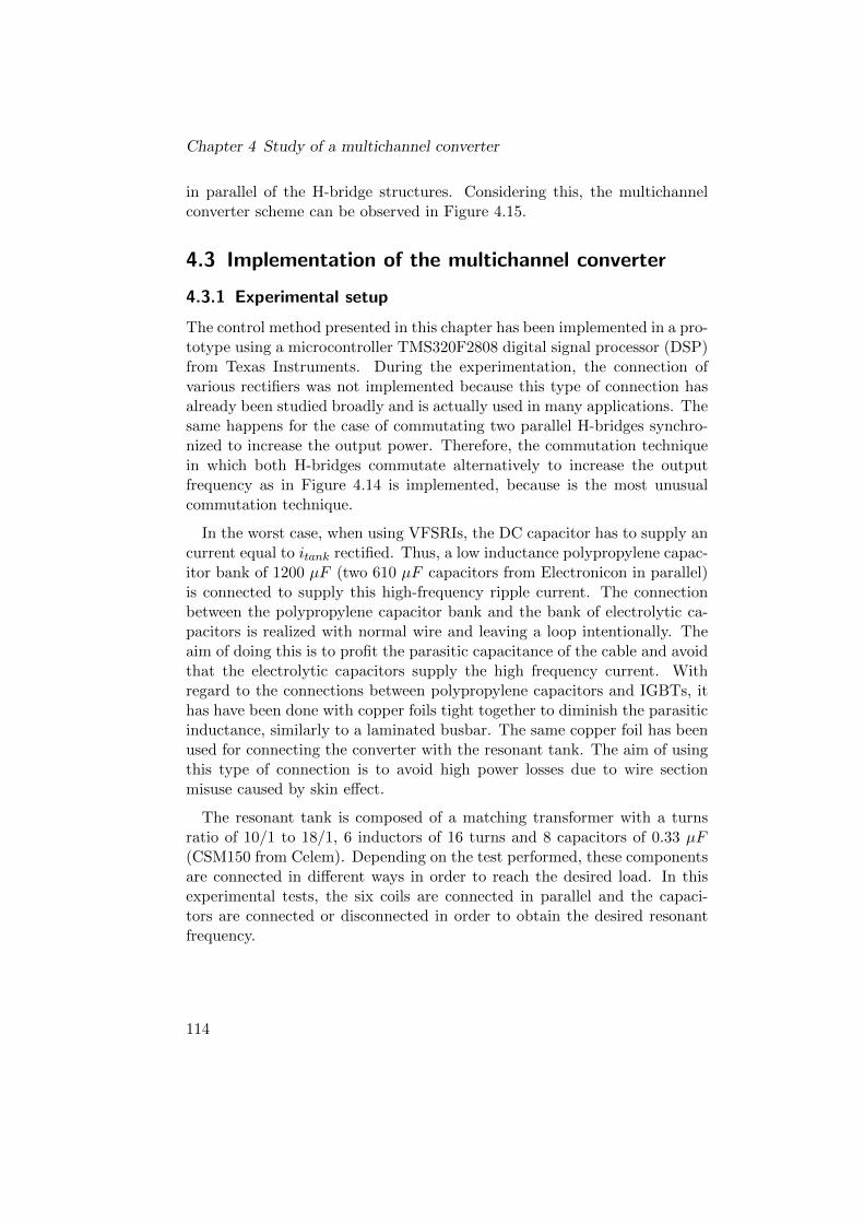
Chapter 4 Study of a multichannel converter
in parallel of the H-bridge structures. Considering this, the multichannelconverter scheme can be observed in Figure 4.15.
4.3 Implementation of the multichannel converter
4.3.1 Experimental setup
The control method presented in this chapter has been implemented in a pro-totype using a microcontroller TMS320F2808 digital signal processor (DSP)from Texas Instruments. During the experimentation, the connection ofvarious rectifiers was not implemented because this type of connection hasalready been studied broadly and is actually used in many applications. Thesame happens for the case of commutating two parallel H-bridges synchro-nized to increase the output power. Therefore, the commutation techniquein which both H-bridges commutate alternatively to increase the outputfrequency as in Figure 4.14 is implemented, because is the most unusualcommutation technique.
In the worst case, when using VFSRIs, the DC capacitor has to supply ancurrent equal to itank rectified. Thus, a low inductance polypropylene capac-itor bank of 1200 µF (two 610 µF capacitors from Electronicon in parallel)is connected to supply this high-frequency ripple current. The connectionbetween the polypropylene capacitor bank and the bank of electrolytic ca-pacitors is realized with normal wire and leaving a loop intentionally. Theaim of doing this is to profit the parasitic capacitance of the cable and avoidthat the electrolytic capacitors supply the high frequency current. Withregard to the connections between polypropylene capacitors and IGBTs, ithas have been done with copper foils tight together to diminish the parasiticinductance, similarly to a laminated busbar. The same copper foil has beenused for connecting the converter with the resonant tank. The aim of usingthis type of connection is to avoid high power losses due to wire sectionmisuse caused by skin effect.
The resonant tank is composed of a matching transformer with a turnsratio of 10/1 to 18/1, 6 inductors of 16 turns and 8 capacitors of 0.33 µF(CSM150 from Celem). Depending on the test performed, these componentsare connected in different ways in order to reach the desired load. In thisexperimental tests, the six coils are connected in parallel and the capaci-tors are connected or disconnected in order to obtain the desired resonantfrequency.
114

ii
“PhD” — 2012/5/21 — 8:58 — page 115 — #76 ii
ii
ii
4.3 Implementation of the multichannel converter
Bridge rectifier
Bridge rectifierDrivers Electrolytic
capacitorsControl board
Polypropylene capacitors
H-bridges
Inductance
Figure 4.16: Experimental setup used for the multichannel converter.
IGBT1 and 3
IGBT2 and 4
IGBT5 and 7
IGBT6 and 8
Figure 4.17: Experimental setup used for the multichannel converter, zoom.
115

Chapter 4 Study of a multichannel converter
Pow
er
supp
ly
23
0 Va
c /
±
15
Vdc
VVVV
L1 L2 L3 N E
VVVV
Re
d lig
ht
SKD
30/
12
3-ph
indu
ctor
6,
4 m
H
Elec
trol
itic
capa
cito
rs
2
x 47
00 u
F
450
VPoly
prop
ylen
e ca
paci
tors
2 x
610
uF
9
00 V
Hal
l-eff
ect
tran
sduc
er
LV-2
5
SKM
100G
B128
DSK
M10
0GB1
28D
Dis
char
ging
re
sist
ors
Hig
h‐fr
eque
ncy
tran
sfor
mer
14:
1
Zero‐c
ross
ing
dete
ctor
Cu
rre
nt
me
asu
rem
ent
Re
son
ant
capa
cito
r
He
atin
g
ind
ucto
r
2 x
Driv
ers
2SC
043
5T2
Pow
er
supp
ly
23
0 Va
c /
24
Vdc
+15
0-1
5
24
0
SW
1SW
2 SW
3SW
4 Ala
rm1 Ue
Opt
ical
fibe
r
Îtank
ADC
Cont
rol b
oard
with
T
MS
320
F28
08
DS
P
u sq
uarei sq
uare
Conv
erte
r un
der
test
Auto
tran
sfor
mer
SKM
100G
B128
DSK
M10
0GB1
28D
Snub
ber
capa
cito
rs
2 x
Driv
ers
2SC
043
5T2
SW
5SW
6 SW
7SW
8A
larm
2
24 0
x7
x5
x2
x2
.pd
f
Fig
ure
4.18
:E
lect
rica
lsc
hem
eof
the
exp
erim
enta
lse
tup
.
116

ii
“PhD” — 2012/5/21 — 8:58 — page 117 — #77 ii
ii
ii
4.3 Implementation of the multichannel converter
The experimental setup is shown in Figures 4.16 and 4.17 and its electricalscheme in Figure 4.18. A three-phase autotransformer is used to set thevoltage Ue to the desired value. In order to ensure a constant voltage value, athree-phase inductor and a 2350 µF capacitor bank (two 4700 µF capacitorsin series) act as a low-pass filter.
4.3.2 Experimental results
The variables measured are shown schematically in Figure 4.19. The outputcurrent of both H-bridges, iHB1 and iHB2, the voltage utank and the cur-rent itank are shown in Figures 4.20 and 4.21. In the first case the resultscorrespond to a 96 kHz resonant tank and in the second case to a 154 kHztank.
In Figures 4.20 and 4.21, it can be observed that the current is flowing onefull period in H-bridge 1 and another full period in H-bridge 2. It can be alsoobserved that during the dead-times the current conducts in both H-bridges.This is caused by the turning-off of all the IGBT during this interval. Underthese circumstances, the current charges the parasitic capacitances of allIGBTs until the antiparallel diodes conduct or the IGBTs’ turn-on.
In Figures 4.22 and 4.23, the input current of both H-bridges, ie1 and ie2,the voltage utank and the current itank are shown for 96 kHz and 154 kHzresonant tanks. It can be observed how the current input of each inverter ishalf of the total itank rectified.
It has to be noted that in the figures presented in this section a super-imposed high frequency ripple is observed in the waveforms. This ripple iscaused by the voltage ringing due to the parasitic components and influencesthe current measurements (realized with Rogowski coils) when measuring thevoltage and the currents at the same time with the same oscilloscope.In thiscase the voltage was measured with a non isolated voltage probe.
During the hardware implementation, the differences between inverter’sconnections have been minimized to avoid voltage drops that can lead to therecirculation of currents between inverters. Although the experimental setupis handmade, it has proven to be reliable and allows the increase of the out-put’s frequency without any recirculation. Several tests have been realizedwith different loads and resonant frequencies obtaining similar results.
The results obtained show that the proper design of the DC-bus andthe connections can permit the industrialization of these basic structures,implementing a multichannel converter formed by diode rectifiers and H-bridges. In this case, SKM100GB128D IGBTs from Semikron were used,
117

Chapter 4 Study of a multichannel converter
Ue
ie1
SW1
SW3 SW4
SW2
SW5
SW7 SW8
SW6
utank
itank
ie2
iHB1
iHB2
Figure 4.19: Variables measured during the experimentation.
utank
(50 V/div)
HB2 conducts
itank
(5 A/div)iHB2
(5 A/div)iHB1
(5 A/div)
HB1 conducts
Figure 4.20: Current at the output of the H-bridges, utank and itank, for aresonant tank of 96 kHz.
118
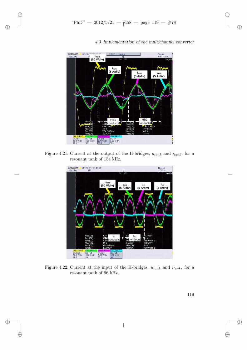
ii
“PhD” — 2012/5/21 — 8:58 — page 119 — #78 ii
ii
ii
4.3 Implementation of the multichannel converter
utank
(50 V/div)
HB2 conducts
itank
(5 A/div) iHB2
(5 A/div)iHB1
(5 A/div)
HB1 conducts
Figure 4.21: Current at the output of the H-bridges, utank and itank, for aresonant tank of 154 kHz.
utank
(50 V/div)
Ie2
conducts
itank
(5 A/div)ie2
(5 A/div)ie1
(5 A/div)
Ie1
conducts
Figure 4.22: Current at the input of the H-bridges, utank and itank, for aresonant tank of 96 kHz.
119
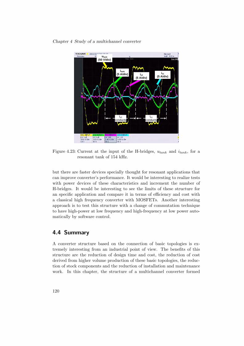
Chapter 4 Study of a multichannel converter
utank
(50 V/div)
Ie2
conducts
itank
(5 A/div) ie2
(5 A/div)
ie1
(5 A/div)
Ie1
conducts
Figure 4.23: Current at the input of the H-bridges, utank and itank, for aresonant tank of 154 kHz.
but there are faster devices specially thought for resonant applications thatcan improve converter’s performance. It would be interesting to realize testswith power devices of these characteristics and increment the number ofH-bridges. It would be interesting to see the limits of these structure foran specific application and compare it in terms of efficiency and cost witha classical high frequency converter with MOSFETs. Another interestingapproach is to test this structure with a change of commutation techniqueto have high-power at low frequency and high-frequency at low power auto-matically by software control.
4.4 Summary
A converter structure based on the connection of basic topologies is ex-tremely interesting from an industrial point of view. The benefits of thisstructure are the reduction of design time and cost, the reduction of costderived from higher volume production of these basic topologies, the reduc-tion of stock components and the reduction of installation and maintenancework. In this chapter, the structure of a multichannel converter formed
120

ii
“PhD” — 2012/5/21 — 8:58 — page 121 — #79 ii
ii
ii
4.4 Summary
by basic topologies is studied, paying special attention to the connectionand commutation techniques of the inverters in order to increase the outputpower and frequency.
The most simple structure to construct an IH converter for a high-powerapplication is by using an uncontrolled bridge rectifier plus an H-bridge. Inthis study, the multichannel converter is formed by one or various uncon-trolled rectifiers and various H-bridges. With regard to the semiconductorsused in the inverters, actually high voltage and high power MOSFET de-vices are already available. However, IGBTs are more common and their usedecreases the number of devices needed and the overall cost of the system.With regard to the type of inverter, the use of VFSRI is advantageous interms of availability of commercial components.
The H-bridge inverters that compose the multichannel converter can beconnected in series or in parallel. The series connection of H-bridges requiresa matching transformer at the output of each inverter, increasing the cost ofthe system. In this case, the output waveform obtained is ±nUe at fsw and±Ue at nfsw. In case of connecting the inverters in parallel, the inverters cancommutate synchronized to increase the power or alternatively to increasethe output frequency. The benefits of the parallel connection are that amatching transformer for every inverter is not required and that allows theincrease of the output frequency, thus, allowing the use of IGBTs in highfrequency applications.
A multichannel converter has been constructed with two H-bridge inver-ters in parallel and has been tested commutating both inverters alternativelyto increase the output’s frequency. The system has shown good reliabilityunder different conditions in which has been tested, proving that this com-mutation technique allows the increase of the output’s frequency withoutany recirculation between inverters. The use of fast IGBTs and the properdesign of the inverters’ connections can allow the implementation of thistype of structure in industrial equipments, allowing the increase of power orfrequency depending on the requirements.
121

122
ii
“PhD” — 2012/5/21 — 8:58 — page 123 — #80 ii
ii
ii
Chapter 5
Design of a software phase-lockedloop
5.1 Introduction
IH converters commutate close to resonant frequency to supply maximumpower to the workpiece. In case of VFSRI and CFPRI, the converter com-mutates slightly above resonance and, in case of converters with LCL tanks,it commutates above the higher of the two resonant frequencies of the tank.Even those IH systems using power control strategies based on shifting outof resonance need to detect which is the resonant frequency. Therefore, thecorrect identification of the tanks’ resonant frequency is a matter of vitalimportance in most IH converters.
A manner of detecting the resonant frequency is by calculating the phase-shift between two electric variables. In case of VFSRI and CFPRI, thephase-shift between voltage and current is zero at resonant frequency, soone method of finding the resonant frequency is varying the frequency untilthe phase-shift is zero. In case of converters with LCL tanks, the base ideais the same, but with a 90 o phase-shift between the voltage at the output ofthe inverter and the voltage at the capacitor. For controlling this phase-shiftbetween two electric variables, most of IH converters use a phase-locked loop(PLL) system.
In this chapter, a software PLL for IH applications is presented, simulatedand implemented in a VFSRI. First, the control principles of PLL systemsapplied to IH are introduced, presenting the proposed software PLL systemand simulating it, in Section 5.2. Then, in Section 5.3, the PLL is imple-mented in a real industrial application and the chapter is summarized inSection 5.4.
123

Chapter 5 Design of a software phase-locked loop
5.2 Software phase-locked loop principles anddescription
5.2.1 Phase-locked loop description and operation principles
A PLL is a circuit that synchronizes a periodic input signal with a periodicoutput signal [89, p. 1]. It is composed of three elements: a phase detector,a low-pass filter and a voltage-controlled oscillator (VCO). The scheme of abasic PLL is shown in Figure 5.1. It is not the aim of this study to explaindeeply the different parts and techniques of implementing a PLL, but somebasic concepts are introduced. Further information can be found in [89].
PhaseDetector
Low-passfilter VCO
Input signal
Signal proportional to the phase-shift
DC voltage proportional to the phase-shift
Ouput signal
Figure 5.1: Basic scheme of a PLL circuit.
As shown in Figure 5.1, the phase detector produces a signal that is pro-portional to the phase-shift between the two input signals. Then, this signalis filtered through a low-pass filter, obtaining a DC voltage that is propor-tional to the phase-shift. Afterwards, a VCO generates an AC signal whosefrequency is proportional to its DC input voltage. In case of a feedback loop,the output of the VCO is connected with the input of the phase detectorand the VCO adjusts the frequency until the output signal is matched tothe input signal.
There are different types of PLLs, depending on the phase detector, thefilter and the VCO. A general classification of them is shown in Figure5.2 [90, p. 8]. Since the first analog PLL integrated circuits appeared in the60’s, PLLs have incorporated more and more digital components. First thedigital PLL appeared, which included digital phase detectors with exclusiveOR gates or flip-flops, and after the all-digital PLL was made, in which all thecomponents were digital. In the last decades, with the development of highperformance microcontrollers and DSPs, PLLs have become all-digital andsoftware implemented. Although digital and all-digital PLLs are still widelyused, software-PLLs have advantages regarding the integration, flexibilityand control’s complexity that with classical PLL systems can be difficult to
124

ii
“PhD” — 2012/5/21 — 8:58 — page 125 — #81 ii
ii
ii
5.2 Software phase-locked loop principles and description
realize.
Considering PLLs and IH applications, PLL systems are used to controlthe phase-shift between two electric variables and reach the resonant fre-quency. Some examples of authors that make use of similar schemes in IHfield are [24,59,91–98].
ANALOG PLL
Digital Phase
Detector
Analog Low-pass
filterVCO
Input signal
Pulse proportional to the phase-shift
DC voltage proportional to the phase-shift
Ouput signal
Analog multiplier
Analog Low-pass
filterVCO
Input signal
Signal proportional to the phase-shift
DC voltage proportional to the phase-shift
Ouput signal
DIGITAL PLL
Digital Phase
Detector
Digital Control
Digital controlled Oscillator
Input signal
Pulse proportional to the phase-shift
Ouput signal
ALL-DIGITAL PLL
Digital Signal
Processor
Input signal
Ouput signal
SOFTWARE-PLL
Figure 5.2: Classification of PLL systems.
In case of VFSRI, the voltage and current phase-shift is close to zeroat resonant frequency. To control this phase-shift, some authors use PLLsystems that just measure itank and use a feedback loop, as shown in Case
125
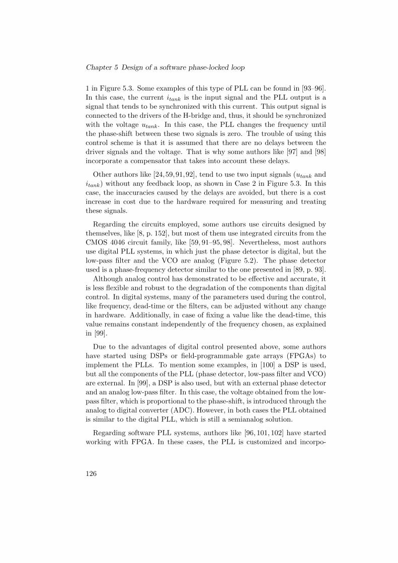
Chapter 5 Design of a software phase-locked loop
1 in Figure 5.3. Some examples of this type of PLL can be found in [93–96].In this case, the current itank is the input signal and the PLL output is asignal that tends to be synchronized with this current. This output signal isconnected to the drivers of the H-bridge and, thus, it should be synchronizedwith the voltage utank. In this case, the PLL changes the frequency untilthe phase-shift between these two signals is zero. The trouble of using thiscontrol scheme is that it is assumed that there are no delays between thedriver signals and the voltage. That is why some authors like [97] and [98]incorporate a compensator that takes into account these delays.
Other authors like [24,59,91,92], tend to use two input signals (utank anditank) without any feedback loop, as shown in Case 2 in Figure 5.3. In thiscase, the inaccuracies caused by the delays are avoided, but there is a costincrease in cost due to the hardware required for measuring and treatingthese signals.
Regarding the circuits employed, some authors use circuits designed bythemselves, like [8, p. 152], but most of them use integrated circuits from theCMOS 4046 circuit family, like [59, 91–95, 98]. Nevertheless, most authorsuse digital PLL systems, in which just the phase detector is digital, but thelow-pass filter and the VCO are analog (Figure 5.2). The phase detectorused is a phase-frequency detector similar to the one presented in [89, p. 93].
Although analog control has demonstrated to be effective and accurate, itis less flexible and robust to the degradation of the components than digitalcontrol. In digital systems, many of the parameters used during the control,like frequency, dead-time or the filters, can be adjusted without any changein hardware. Additionally, in case of fixing a value like the dead-time, thisvalue remains constant independently of the frequency chosen, as explainedin [99].
Due to the advantages of digital control presented above, some authorshave started using DSPs or field-programmable gate arrays (FPGAs) toimplement the PLLs. To mention some examples, in [100] a DSP is used,but all the components of the PLL (phase detector, low-pass filter and VCO)are external. In [99], a DSP is also used, but with an external phase detectorand an analog low-pass filter. In this case, the voltage obtained from the low-pass filter, which is proportional to the phase-shift, is introduced through theanalog to digital converter (ADC). However, in both cases the PLL obtainedis similar to the digital PLL, which is still a semianalog solution.
Regarding software PLL systems, authors like [96, 101, 102] have startedworking with FPGA. In these cases, the PLL is customized and incorpo-
126

ii
“PhD” — 2012/5/21 — 8:58 — page 127 — #82 ii
ii
ii
5.2 Software phase-locked loop principles and description
Phase Comparator
Voltage-controlled oscillator
Low-pass filter
Zero-Crossing Detector
Zero-Crossing Detector
isquare Phase-shift
pulses
Voltage proportional
to phase-delay
Comparator
Comparator
usquare
Case 1
Phase Comparator
Voltage-controlled oscillator
Low-pass filter
Zero-Crossing Detector
Signal to drivers
isquare Phase-shift
pulses
Voltage proportional
to phase-delay
Comparator
Case 2
Compensator
Theoretical utank(from VCO)
Theoretical utankdelayed
Signal to drivers
utankUe Req
L
C+
-
+
+-
-
Voltage-fed inverter
uC
uReq
uL
Resonant tank
RCsnubber
Gate signals to switches
itank
(measured)utank
(measured)
itank
SW1 SW2
SW3 SW4
itank
(measured)
itank
(measured)
utank
(measured)
Figure 5.3: Block diagram of the PLL systems used in IH.
127

Chapter 5 Design of a software phase-locked loop
rates the filter, as-well as the digital oscillator. Although the incorporationof FPGA allows a fast digital signal processing, the difficulty in the pro-gramming is still a barrier and justifies the use of commercial DSP.
5.2.2 Software phase-locked loop for induction heating
Nowadays, there are many microcontroller manufacturers like Microchip, In-fineon, Freescale and Texas Instruments, that provide their microcontrollerswith the capacity to detect falling and rising edges. This detection is realizedthanks to the capture or edge detector module that is incorporated in themicrocontrollers and assigned to some of their pins. The control scheme pro-posed in this section takes advantage of this module, integrating the phasecomparator, the low pass filter, the VCO, the compensator and a PI regu-lator in the same microcontroller. In Figure 5.4, the basic scheme of thissoftware-PLL is shown.
To have a more precise control, both signals utank and itank are acquired.These signals are measured and conditioned to obtain a synchronized square-waveform in the voltage range of the microcontroller (usquare and isquare).Then, the rising edges of these signals are acquired by the microcontroller’sedge detector (CAP1A register for the voltage and CAP2A register for thecurrent). In this case, the time delay tϕ is used instead of the phase-shift ϕand it is obtained by subtracting the values obtained from the edge detectorand multiplying it by the time clock of the counter (tclock). Afterwards, thisvalue is introduced in a PI controller and compared to a reference delay timet∗ϕ. The commutation frequency is obtained at the output of the PI, changingthe register corresponding to this parameter in the microcontroller. In thiscase, the control method takes advantage of the built-in PWM generatorsprovided by the microcontroller, allowing an easy change of the commutationfrequency as well as the dead-time.
tφ =(CAP2A-CAP1A)*tclock
PI Commutationfrequency
tφ* +
Start edge detection
timetclock
Co
unte
r
Edge detector
isquare
usquare
CAP1ACAP2A
Zero-Crossing Detector
itank
(measured)
Comparator
utank
(measured)
Gate signals
to drivers
Dead-time*
Microcontroller
Zero-Crossing Detector
Comparator
Figure 5.4: Software-PLL based on a DSP microcontroller.
128

ii
“PhD” — 2012/5/21 — 8:58 — page 129 — #83 ii
ii
ii
5.2 Software phase-locked loop principles and description
This software PLL permits controlling the converter with less analog com-ponents and thus, with less variations due to part spread or temperaturedrift. However, the major benefit of this system is the easy programming andthe flexibility provided to the equipment, since all the parameters (phase-shift reference, PI constants, frequency limits, starting frequency, dead-time,etcetera) can be changed and adapted to different conditions just by modi-fying the software.
It has to be noted that that the precision of this system relies on the timeclock of the microcontroller, which marks the minimum phase-shift that canbe detected.
5.2.3 Simulations
Simulation model
The model simulated is a VFSRI with an H-bridge composed of 4 MOSFETswith the parameters shown in Table 7.1.
Table 5.1: Parameters of the simu-lated system.
Parameter Value
Capacitance 5.62 nFResonant tank Inductance 154 µH
Resistance 5.75 ΩResonant frequency 170.82 kHz
Mosfet Parasitic capacitance 4.2 nFSnubber Capacitance 30 nF
Resistance 26.6 Ω
The system is modeled with MATLAB-SIMULINK c© using the schemeshown in Figure 5.5. In this case, when utank crosses zero, there is a risingedge and the edge detector memorizes the counter value in the CAP1Aregister. The same occurs with the current itank in the CAP2A register.This value is hold by a sample and hold register and the counter is reseatedevery cycle. This reseat is realized at 0.5/fsw seconds after the start ofevery cycle to avoid its coincidence with a commutation. The frequency ofthe time base counter is set to 100 MHz and, thus, the minimum time delaythat can be computed is 10 ns (tclock).
In Section 3.2.5, it was explained that the inverters usually commutate at ahigher frequency than the resonant frequency to avoid the reverse recovery
129

Chapter 5 Design of a software phase-locked loop
of diodes (inductive switching). Therefore, during these simulations, theinitial switching frequency is set to 175 kHz and the time delay reference ispositive.
Two cases have been simulated to illustrate the influence of the time delayand dead-time in the control’s performance:
• Case 1: The system is simulated with a low dead-time and time delay,0.290 µs and 0.117 µs respectively.
• Case 2: The system is simulated with a high dead-time and time delay,0.550 µs and 0.294 µs respectively.
Zero-Crossing Detector
Zero-Crossing Detector
isquare
itank(measured)
Comparator
Comparator
usquare
CAP1A
Start edge detection
timetclock
Cou
nter
S/H
S/H
+
-
tφPI
+
tφ*
Frequency limits
VCODead time generator
Dead-time*
Gate signals
to drivers
utank(measured)
CAP1A
CAP2A
CAP2A fsw
-
Edge detector
X tclock
Figure 5.5: Scheme of the modeled system.
Simulation results
In Figure 5.6, the capture module output for the rising edges (CAP1A forthe voltage and CAP2A for the current), the measured time delay betweenvoltage and current and the switching frequency are shown for Case 1 (lowdead-time and time delay reference). Figure 5.8 shows the zoom of thesame parameters when the steady-state is reached and Figure 5.10 showsutank and itank, their synchronous square-waveforms and the counter andthe capture modules for the rising edges. Figures 5.7, 5.9 and 5.11 show thesame variables for Case 2 (high dead-time and time delay reference).
Observing the commutation frequency in Figures 5.6 (Case 1) and 5.7(Case 2), the frequency starts at 175 kHz in both cases and the behavior issimilar. However, in Case 2, the register corresponding to the voltage risingedge (CAP1A) and the time delay have abrupt variations. In case of theregister corresponding to the current rising edge (CAP2A), the value is quitestable and with a similar behavior in both cases.
130
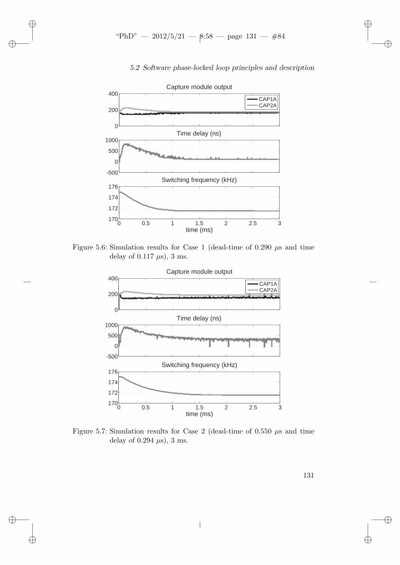
ii
“PhD” — 2012/5/21 — 8:58 — page 131 — #84 ii
ii
ii
5.2 Software phase-locked loop principles and description
0
200
400Capture module output
CAP1ACAP2A
-500
0
500
1000Time delay (ns)
0 0.5 1 1.5 2 2.5 3170
172
174
176
time (ms)
Switching frequency (kHz)
Figure 5.6: Simulation results for Case 1 (dead-time of 0.290 µs and timedelay of 0.117 µs), 3 ms.
0
200
400Capture module output
CAP1ACAP2A
-500
0
500
1000Time delay (ns)
0 0.5 1 1.5 2 2.5 3170
172
174
176
time (ms)
Switching frequency (kHz)
Figure 5.7: Simulation results for Case 2 (dead-time of 0.550 µs and timedelay of 0.294 µs), 3 ms.
131

Chapter 5 Design of a software phase-locked loop
140
160
180
200Capture module output
CAP1ACAP2A
-200
0
200
400Time delay (ns)
1.5 2 2.5 3
171.5
171.55
171.6
time (ms)
Switching frequency (kHz)
Figure 5.8: Simulation results for Case 1 (dead-time of 0.290 µs and timedelay of 0.117 µs), steady-state from 1.5 to 3 ms.
140
160
180
200Capture module output
CAP1ACAP2A
-200
0
200
400Time delay (ns)
1.5 2 2.5 3
171.5
171.55
171.6
time (ms)
Switching frequency (kHz)
Figure 5.9: Simulation results for Case 2 (dead-time of 0.550 µs and timedelay of 0.294 µs), steady-state from 1.5 to 3 ms.
132
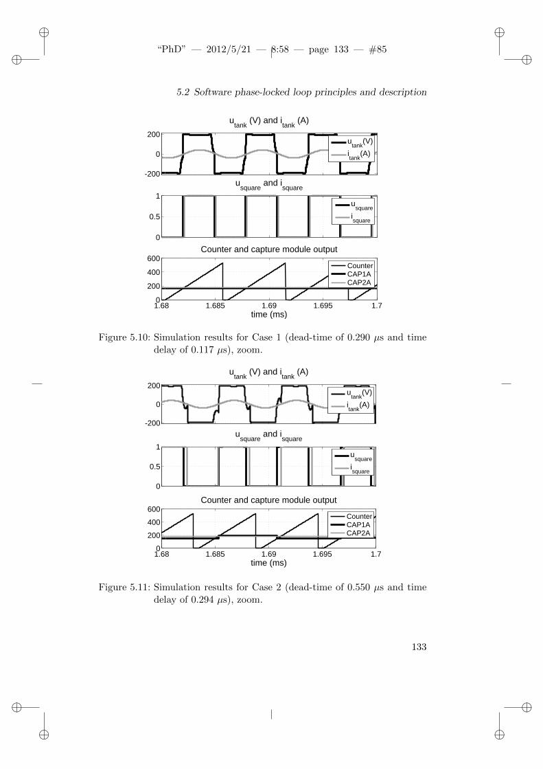
ii
“PhD” — 2012/5/21 — 8:58 — page 133 — #85 ii
ii
ii
5.2 Software phase-locked loop principles and description
-200
0
200
utank
(V) and itank
(A)
utank
(V)
itank
(A)
0
0.5
1
usquare
and isquare
usquare
isquare
1.68 1.685 1.69 1.695 1.70
200
400
600
time (ms)
Counter and capture module output
CounterCAP1ACAP2A
Figure 5.10: Simulation results for Case 1 (dead-time of 0.290 µs and timedelay of 0.117 µs), zoom.
-200
0
200
utank
(V) and itank
(A)
utank
(V)
itank
(A)
0
0.5
1
usquare
and isquare
usquare
isquare
1.68 1.685 1.69 1.695 1.70
200
400
600
time (ms)
Counter and capture module output
CounterCAP1ACAP2A
Figure 5.11: Simulation results for Case 2 (dead-time of 0.550 µs and timedelay of 0.294 µs), zoom.
133
Chapter 5 Design of a software phase-locked loop
These sudden changes in CAP2A and in the time delay can be betterobserved in Figures 5.8 and 5.9, which are a zoom of the same variablesbetween 1,5 and 3 ms. Observing these figures, there is a sudden changein CAP1A value for Case 2. This sudden change causes variations in thetime delay value and in the commutation frequency, fact that is reasonableconsidering the control presented in Figure 5.5.
The abrupt change of CAP1A value in Case 2 is due to the shape of thevoltage waveform utank, which is not monotonous during the commutation.Observing Figure 5.10, in the Case 1, utank has a monotonous rising slopeduring the commutation. That occurs because the dead-time is low and theturn-on of switches SW1 and SW4 occur before the current itank changespolarity. Consequently, CAP1A value is quite constant. Observing Figure5.11 for Case 2, the voltage utank has a non monotonous rising slope duringthe commutation. That is because the dead-time is too high and the currentchanges polarity,discharging the parasitic capacitances before the turn-on ofSW1 and SW4. This change in the slope cause unwanted, though not critical,variations in the phase-shift and, thus, in the commutation frequency.
Case 2 represents a limit situation because this change of slope takes placeclose to zero. Thus, depending if it occurs before or after utank changes po-larity, it creates a great variation on CAP1A register, as shown in Figure5.11.During normal operation, this situation is not common because dead-time references are low. Moreover, the larger the phase-shift (time delay),the larger the switched current and, thus, the chances that the voltage polar-ity is reversed are reduced. Nevertheless, it has to be taken into considerationto avoid potential uncontrolled situations. Thanks to the flexibility of thesoftware PLL, this situation can be prevented with the configuration of analarm that warns that two zero-crossings are too close to each other. Thisalarm would warn the user that the dead-time and phase-shift values shouldbe changed.
5.3 Implementation and experimental results
The microcontroller chosen to implement the software PLL is a TMS320-F2808 DSP from Texas Instruments [103]. This microcontroller integratesall the peripherals needed (PWM, ADC, digital to analog converters andcommunications) and is flexible for reprogramming, fast in treating digitalsignals and sturdy against perturbations. It also incorporates an enhancedcapture module (eCAP module) with a 32-bit time base and 100 MHz sys-tem clock, 4 event time-stamp registers (each of 32 bits) and edge polarity
134

ii
“PhD” — 2012/5/21 — 8:58 — page 135 — #86 ii
ii
ii
5.3 Implementation and experimental results
selection that can be used for implementing the software PLL. Even thoughthis control can be realized easily with this DSP, it has to be noted that itsimplementation can be also realized with other DSPs or with FPGAs withhigher computing performance.
The control has been tested in a real industrial application of continuouswire heating with a converter designed by CITCEA-UPC, shown in Figure5.12. The system is a 25 kVA and 250 kHz converter with a series resonanttank with similar characteristics to the simulated in the previous section inTable 5.1.
Figure 5.12: Equipment tested in an industrial application of continuouswire heating.
A simplified diagram of the implemented control is shown in Figure 5.13.This control scheme is based on the proposed control in Figure 5.4. Thevoltage and current square-waveforms usquare and isquare, obtained fromutank and itank, are connected to the capture unit of the microcontrollerand the instant at which their rising/falling edges occur are memorized inregisters (CAP1A and CAP1B registers for the voltage and CAP2A andCAP2B for the current). In this case, there is an interruption activatedby the time base of the PWM at 0.75/fsw that calculates the time delay(tϕ), calculates the switching frequency, updates the registers and reseatsthe counter. The time delay between voltage and current is calculated withthe average value of the substraction of registers CAP2A minus CAP1A andCAP2B minus CAP1B. Then this value is multiplied by tclock (10 ns). It
135

Chapter 5 Design of a software phase-locked loop
Time delay is correct ?
CAP1A
CAP1B
CAP2A
CAP2B
Start edge detection
isquare
usquare
Correction of delays due to measurements delays
CAP2A = CAP2A+ tdsystem
CAP2B = CAP2B+ tdsystem’
time
time
time
abs(CAP1A – CAP1B)·tclock< 0.5· 1/(fsw)abs(CAP2A – CAP2B)·tclock< 0.5· 1/(fsw)
YES
NO
Error
Calculate time delay
Warning if repeated
Limited PI regulator
Reset counter and capture events counter
Update PWM frequency
tclock
tφ = 0.5·[(CAP2A – CAP1A)+(CAP2B – CAP1B)]·tclock
tφ*
Initial commutation frequencyDead-time*
fsw
CAP1A, CAP1B, CAP2A, CAP2BCAP registers
Interruption at 0.75· 1/(fsw) of the base for PWM (usquare)
Interruption Interruption
Figure 5.13: Control scheme implemented in the microcontroller.
can be observed in this figures how there is a small correction of the timedelays due to the delays of the measurements (amplifiers, fiber optic) whichis computed by adding a delay to CAP2 registers.
To validate that the time delay acquired is correct it has to be verifiedthat the difference between two rising/falling edges is higher than half of thecommutation period (1/fsw). If the difference is minor it means that bothrising/falling edges are too close to each other, the frequency is not variedand an error counter increases. In case that this error counter arrives toa limit defined by the user, the control stops the converter’s operation andwarns the user.
This error can occur when the initial commutation frequency is far awayfrom the resonant frequency and the current is so small that generates falsezero-crossings. In this case, the user just has to change the initial com-mutation frequency register until the system is able to track the resonantfrequency. Another situation that can lead to this error, is the case describedin Case 2 during the simulations, in which the voltage rising slope crosseszero twice.
One of the advantages of this software PLL is that allows the user to
136
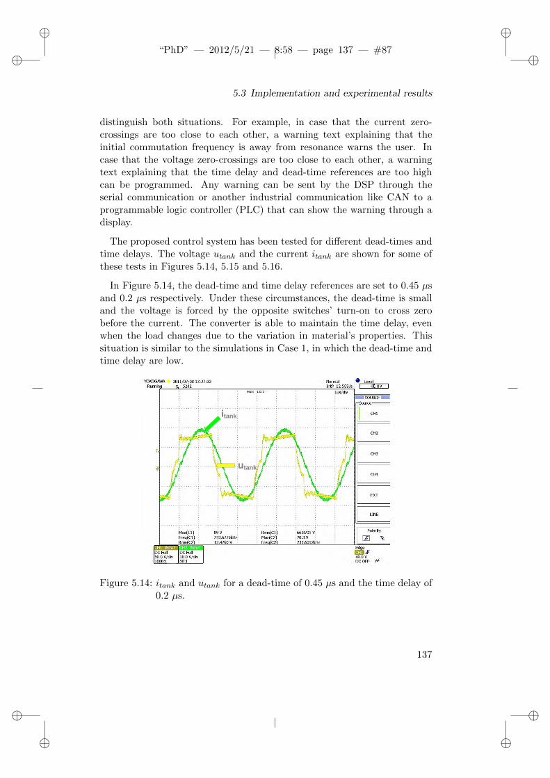
ii
“PhD” — 2012/5/21 — 8:58 — page 137 — #87 ii
ii
ii
5.3 Implementation and experimental results
distinguish both situations. For example, in case that the current zero-crossings are too close to each other, a warning text explaining that theinitial commutation frequency is away from resonance warns the user. Incase that the voltage zero-crossings are too close to each other, a warningtext explaining that the time delay and dead-time references are too highcan be programmed. Any warning can be sent by the DSP through theserial communication or another industrial communication like CAN to aprogrammable logic controller (PLC) that can show the warning through adisplay.
The proposed control system has been tested for different dead-times andtime delays. The voltage utank and the current itank are shown for some ofthese tests in Figures 5.14, 5.15 and 5.16.
In Figure 5.14, the dead-time and time delay references are set to 0.45 µsand 0.2 µs respectively. Under these circumstances, the dead-time is smalland the voltage is forced by the opposite switches’ turn-on to cross zerobefore the current. The converter is able to maintain the time delay, evenwhen the load changes due to the variation in material’s properties. Thissituation is similar to the simulations in Case 1, in which the dead-time andtime delay are low.
tank
tank
Figure 5.14: itank and utank for a dead-time of 0.45 µs and the time delay of0.2 µs.
137

Chapter 5 Design of a software phase-locked loop
tank
tank
Figure 5.15: itank and utank for a dead-time of 0.51 µs and the time delay of0.2 µs.
tank
tank
Figure 5.16: itank and utank for a dead-time of 0.75 µs and the time delay of0.3 µs.
138

ii
“PhD” — 2012/5/21 — 8:58 — page 139 — #88 ii
ii
ii
5.3 Implementation and experimental results
In Figure 5.15, the dead-time is increased to 0.51 µs. In this case, utankreaches Ue, the diodes are forward-biased and the transistors are turned-onwith ZVS. Then the current changes polarity and the diodes are blocked withZCS. This is the optimal commutation sequence for a VFSRI, as explainedin Section 3.2.5.
In Figure 5.16, the dead-time is increased to 0.75 µs. Under these cir-cumstances, the voltage slope is not monotonous and the change of slopeis close to zero, similar to Case 2 during the simulations. In this case, thecontrol detects voltage rising edges too close to each other, the commuta-tion frequency is not varied and the PLL warns the user. Many tests havebeen performed with different references and uncontrolled situations havenot occurred.
During the experimentation, the software PLL has been tested with dif-ferent tanks, voltages, currents and references, showing a good performanceunder different situations. It has been observed that the results obtained aresimilar to those obtained during the simulations, solving the case at whichthe voltage slope is not monotonous. It has also been observed that thesystem is able to reach a time delay reference, even when the initial commu-tation frequency is a 25 % higher than the resonant frequency. Moreover, incase the initial frequency is too far from the resonant frequency and thereare false current’s zero-crossings, the converter warns the user and the ini-tial frequency can changed by software through a preprogrammed humanmachine interface. The control system has been tested with tanks in therange of 50 kHz to 250 kHz without any change in converter’s hardware andobtaining good performance results.
The major benefit of this control system is to allow a great flexibility, asall the parameters can be changed dynamically by software (dead-time, timedelay, starting frequency, etcetera). Therefore, this system provides moreflexibility and adaptability to different situations compared to the classi-cal control methods introduced in Section 5.2. Moreover, the possibility ofchanging dynamically the variables blazes the way to the programming ofmore complex control algorithms, as for example an optimal commutationsequence similar to the explained in Section 3.2.5.
It has to be noted that the control system presented is verified for a VFSRI,but can be also used for CFPRI. The only change that must be realized isthe measuring and adaptation of signals.
139

Chapter 5 Design of a software phase-locked loop
5.4 Summary
In IH, the converter measures and imposes the phase-shift between two sig-nals for commutating at resonant frequency. In case of VFSRI, the convertermeasures the phase-shift between utank and itank and varies the frequencyuntil the phase-shift is approximately zero. This control is realized by theconverter thanks to a PLL system.
Most authors in IH field use semianalog PLL systems to control the con-verter, the majority based on the CMOS 4046 integrated circuit family.These systems are affected by the spread of component parameters, compo-nent degradation or variation with temperature. Moreover, in case of loadchanges, the systems have to be tuned. Considering all-digital or softwarePLL systems, there are very few experiences in IH field, most of them usingFPGA.
In this chapter, a DSP-based software PLL is proposed. This controlsystem measures the phase-shift by acquiring the rising edges of voltageand current with the edge detector provided by the microcontroller. Thissoftware PLL allows a control with less analog components, avoiding theirdrawbacks and offering more flexibility to the system.
The proposed software PLL has been simulated, noticing that in case oflarge time delays and dead-times, utank has a non-monotonous slope duringthe commutation which can cause sudden changes in the control variables.
The software PLL has been tested in a real industrial application of con-tinuous wire heating and the control instability detected in the simulationshas been solved by software. The converter detects when the difference be-tween two rising edges is lower than half of the commutation’s period andthe user is warned.
The system has been tested with different tanks and references, providinga good response for different conditions and evidencing its flexibility in areal industrial application. The converter allows the final user to changethe parameters by software, in this case through a PLC connected to theDSP. The system also permits a better adaptation of the converter to diverserequirements, an easy implementation and the use of debugging systems thatallow faster designing. Moreover, it opens the way to more complex controlalgorithms, since the time delay, dead-time, frequency and other parameterscan be changed dynamically during the heating process.
140

ii
“PhD” — 2012/5/21 — 8:58 — page 141 — #89 ii
ii
ii
Chapter 6
Design of a load-adaptivephase-locked loop
6.1 Introduction
IH converters commutate close to resonant frequency to obtain the maximumpower and reduce switching losses. In case of VFSRI, the commutationprocess is determined by the transistor’s parasitic capacitors, snubbers andlayout capacitance. These capacitances have to be charged before the turn-on of the transistors and the change of polarity of the load’s current to ensuresoft-switching. To ensure this sequence, the phase-shift and the dead-timehave to vary depending on the load.
In this chapter, a load-adaptive PLL based on the software PLL explainedin Chapter 5 is presented. This control system allows the variation of thephase-shift and the dead-time to ensure soft-switching. First, in Section6.2, the commutation process is explained, presenting the proposed controlsystem and simulating it. Afterwards, in Section 6.3, the implementation ofthis system is exposed and the experimental results are presented. Finally,the chapter is summarized in Section 6.4.
6.2 Commutation process and load-adaptivephase-locked loop description
6.2.1 Commutation process
In Section 3.2.5, the influence of the parasitic capacitances (including tran-sistor’s parasitic capacitors, snubbers and layout capacitances) during thecommutation process is exposed. It is shown that, to have transistor’s ZVSand antiparallel diodes’ ZCS, Equations 3.21 and 3.22 have to be accom-plished for β and ϕ. Taking this into consideration, in Figure 6.1, the com-
141

Chapter 6 Design of a load-adaptive phase-locked loop
mutation process considering the parasitic capacitances, the dead-time (td)and phase-shift (tϕ) is shown.
utank equals Ue
Diodes D1 and D4 start conducting
Ue
itank
utank
t
State IV State V State VI State I
itank reacheszero and D1 andD4 turn-off softly
Hard turn-off of SW2 and SW3
SW1 and SW4 areturned-on in ZVS
0
t
Gate signals SW1 and SW4
Gate signals SW2 and SW3
β (tβ)
utank reacheszero
t0 t1
Ie
Ue
SW3 SW4
SW2
D3
D2
D4
utank
itank
SW1 D1Cp
Electrical scheme consideringparasitic capacitances
iD1uSW2
phase-shift φ (tφ)
dead-time (td)
tDon
Figure 6.1: Output waveforms and sequence to have ZVS and ZCS commu-tating above resonance considering dead-time and phase-shift.
The sequence of events to have soft-switching is the following:
• Switches SW2 and SW3 turn-off hardly.
• The parasitic capacitance, Cp, of SW2 and SW3 charge, while Cp ofswitches SW1 and SW4 discharge. The voltage utank reaches Ue.
• Diodes D1 and D4 are forward-biased at tDon.
142

ii
“PhD” — 2012/5/21 — 8:58 — page 143 — #90 ii
ii
ii
6.2 Commutation process and load-adaptive phase-locked loop description
• Switches SW1 and SW4 are turned-on at td with ZVS because theirantiparallel-diodes are conducting.
• The current itanc changes polarity at tϕ, blocking the antiparallel-diodes D1 and D4 with ZCS.
Equations 3.21 and 3.22 are obtained supposing the limit situation atwhich the diodes are forward-biased, the switches’ turned-on and the changeof polarity of itank are immediately consecutive (Appendix B). That is
tDon ≈ td ≈ tβ (6.1)
Therefore, considering td and tϕ instead of β and ϕ, Equations 3.21 and3.22 turn into
td ≥1
ωarccos
(1− 2ωUeCp
itank
)(6.2)
and
tϕ ≥1
ωarccos
(1− ωUeCp
itank
)(6.3)
Observing these equations, it is noticed that the control has to adapt thedead-time and phase-shift to the load conditions to ensure soft-switching.Nevertheless, most authors do not incorporate the effect of this capacitanceduring their control, e.g. [99].
Some authors describe and analyze the influence of this capacitance fordifferent operating conditions, like in [104–106]. In case of [59], this influenceis considered in the control by introducing a constant phase-shift delay for anominal condition. In [65], the minimum dead-time is calculated consideringthe capacitor’s influence, but it is still constant and calculated for a nominalcondition. Finally, some authors suggest a load-adaptive control, in whichthe phase-shift varies linearly depending on the current in [64] or dependingon the charge of an equivalent capacitor in [35, p. 96]. However, in allof them, the control is based on analog circuits and the implementationis complex, nonflexible and subjected to the degradation and part spread,typical of analog components.
6.2.2 Load-adaptive phase-locked loop
In order to overcome the drawbacks derived from an analog load-adaptivecontrol, the software PLL presented in Chapter 5 has been used. This PLL
143

Chapter 6 Design of a load-adaptive phase-locked loop
is all-digital and is implemented by software, allowing an easier and moreflexible implementation.
The basic scheme of the control system proposed is shown in Figure 6.2.In this case, the control variables are the current itank, the voltage utank andthe power supply voltage Ue. The equivalent capacitance of the switches(Cp) is supposed to be constant and the phase-shift (tϕ) and dead-time (td)references are set according to the load conditions imposed by Equations6.2 and 6.3. The phase-shift is measured using the edge detector providedby the microcontroller. Then, it is compared with the reference and a PIcontroller is used for calculating the commutation frequency. Finally, thegate signals to drivers incorporating the dead-time reference are obtained.
tφ =(CAP2A-CAP1A) tclock
PI Commutationfrequency
tφ* +
Start edge detection
timetclock
Coun
ter
Edge detector
isquare
usquare
CAP1ACAP2A
Zero‐Crossing Detector
itank
(measured)
Comparator
utank
(measured)
Gate signals
to drivers
td*
Microcontroller
Zero‐Crossing Detector
Comparator
Peakmeasure
ment
Ue
(measured)
Cp
td* tφ
* f
îtank
Ue
Cp ≥
≥
-
Figure 6.2: Proposed load-adaptive PLL.
6.2.3 Simulations
Simulation model
In Figure 6.3, the scheme used for simulating the load-adaptive PLL isshown. Bearing in mind that the minimum td and tϕ to have soft-switchingare obtained from the equalities contained in Equations 6.2 and 6.3, thevalues of td and tϕ have to be higher. Thus, during the simulation, thedead-time and phase-shift are calculated according to these equalities, butthe result is increased by a gain, kd for the dead-time and kϕ for the phase-shift.
144

ii
“PhD” — 2012/5/21 — 8:58 — page 145 — #91 ii
ii
ii
6.2 Commutation process and load-adaptive phase-locked loop description
It can also be observed in this figure that itank is limited. The aim of thislimitation is to avoid low currents that can compute high dead-times andphase-shift values. As regards to the dead-time reference, it is also limited,but in this case with the aim to avoid a lower value than the minimum dead-time that can cause short-circuit. The phase-shift is also limited to avoidnegative phase-shifts that can cause capacitive switching and the frequencyis limited to the inverters’ frequency range.
Start edge detection
timetclock
Coun
ter
Edge detector
isquare
usquare
CAP1ACAP2A
Zero‐Crossing Detector
itank
(measured)
Comparator
utank
(measured)
Zero‐Crossing Detector
Comparator
Peakmeasure
ment
Ue
(measured)
Cp
td*
tφ
îtank
Ue
Cp
S/H
S/H
+-
φPI
+
flimits
VCODead time
generator
Gate signals
to drivers
CAP1A
CAP2A f-
tφ*
tclock
td*
gain
tφ*
gain
kd
=
=
îtank
limitstφ
*
limits
kφ
td*
limits
Figure 6.3: Simulation of the load-adaptive PLL.
Table 6.1: Parameters of the simu-lated system.
Parameter Value
Capacitance 10.38 nFResonant tank Inductance 34.97 µH
Resistance 9.82 ΩResonant frequency 83.53 kHz
itank Upper limit 42 ALower limit 3 A
tϕ Upper limit 10 µsLower limit 0.2 µs
td Upper limit 2.5 µsLower limit 0.1 µs
Upper limit 100 kHzf Lower limit 70 kHz
Initial 84.5 kHz
The control has been simulated with MATLAB-SIMULINK c© and theparameters of this simulation are shown in Table 6.1. It has to be noted
145

Chapter 6 Design of a load-adaptive phase-locked loop
that the initial frequency is set higher than the resonant frequency to avoidcapacitive switching.
Simulation results
The system has been simulated for different voltages and parasitic capac-itances (Cp) to evaluate the control’s performance. Figure 6.4 shows thecurrent Itank in RMS, the phase-shift reference t∗ϕ and the dead-time refer-ence t∗d for the case with the voltage Ue equal to 100 V and Cp 15 nF. Forthe same case, utank, itank, the current in the antiparallel-diode of SW1, thegate signals of SW1 and the zero-crossing of itank are plotted in Figure 6.5.In Figures 6.6 and 6.7, the same variables as in Figure 6.4 are shown, butvarying the voltage Ue to 30 V and 200 V respectively. Finally, Figures 6.8and 6.9 show the same variables, but at 100 V and with different Cp values,25 nF and 35 nF respectively.
During the simulations, it was observed that, for the case in which kϕand kd are equal to 1, the current itank changes polarity before the switches’turn-on. This change of polarity happens almost at the same time as theturn-on, so, to allow the optimum sequence of events (seen in Section 6.2.1),the phase-shift gain (kϕ) is increased to 1.05.
In Figure 6.4, the current value increases arriving to a steady-state. Thephase-shift and dead-time values do not vary much during this process andneither does the frequency. Observing Figure 6.5, the antiparallel-diode D1is forward-biased, afterwards the transistor SW1 turns-on and, then, thecurrent itank changes polarity, thus, having soft-switching.
In case of decreasing the voltage Ue to 30 V, shown in Figure 6.6, orincreasing it to 200 V, shown in Figure 6.7, the phase-shift and dead-timesare almost equal at the steady-state. The current value is different for thethree cases (Figures 6.4, 6.6 and 6.7), but the voltage-current ratio is almostthe same. That is because the load at the resonant frequency is equal to theresistance of the tank (Section 3.2.1). Thus, the ratio is constant in the threecases and so it is the phase-shift and the dead-time if the other parametersare maintained constant, as shown in Equations 6.2 and 6.3.
In case of increasing the parasitic capacitance Cp to 25 nF and 35 nF,Figures 6.8 and 6.9 respectively, the phase-shift and dead-time increase. Thehigher the value of the capacitance, the higher the values of phase-shift anddead-time. Thus, there is a slight increase of 750 Hz on the commutationfrequency in Figure 6.9 compared to Figure 6.8.
146

ii
“PhD” — 2012/5/21 — 8:58 — page 147 — #92 ii
ii
ii
6.2 Commutation process and load-adaptive phase-locked loop description
0
5
10
Itank
(Arms)
0
100
200
300Phase-shift and dead-time (ns)
phase-shift measuredphase-shift referencedead-time reference
0 1 2 3 4 5 6 784
85
86
time (ms)
Commutation frequency (kHz)
Figure 6.4: Simulation results for Ue 100 V and Cp 15 nF, 7 ms.
-200
-100
0
100
200
utank
(V) and itank
(A)
utank
itank
0
2
4
iD1
(A)
6.8065 6.807 6.8075 6.808 6.8085 6.809 6.8095 6.810
0.5
1
time (ms)
Gate signal of SW1 and isquare
Gate signal SW1isquare
Figure 6.5: Simulation results for Ue 100 V and Cp 15 nF, steady-state from6.8065 to 6.81 ms.
147

Chapter 6 Design of a load-adaptive phase-locked loop
0
10
20
Itank
(Arms)
0
100
200
300Phase-shift and dead-time (ns)
phase-shift measured
phase-shift reference
dead-time reference
0 1 2 3 4 5 6 784
85
86
time (ms)
Commutation frequency (kHz)
Figure 6.6: Simulation results for Ue 30 V and Cp 15 nF, 7 ms.
0
10
20
Itank
(Arms)
0
100
200
300Phase-shift and dead-time (ns)
phase-shift measured
phase-shift reference
dead-time reference
0 1 2 3 4 5 6 784
85
86
time (ms)
Commutation frequency (kHz)
Figure 6.7: Simulation results for Ue 200 V and Cp 15 nF, 7 ms.
148

ii
“PhD” — 2012/5/21 — 8:58 — page 149 — #93 ii
ii
ii
6.2 Commutation process and load-adaptive phase-locked loop description
0
5
10
Itank
(Arms)
0
100
200
300Phase-shift and dead-time (ns)
phase-shift measured
phase-shift reference
dead-time reference
0 1 2 3 4 5 6 784
85
86
time (ms)
Commutation frequency (kHz)
Figure 6.8: Simulation results for Ue 100 V and Cp 25 nF, 7 ms.
0
5
10
Itank
(Arms)
0
100
200
300Phase-shift and dead-time (ns)
phase-shift measured
phase-shift reference
dead-time reference
0 1 2 3 4 5 6 784
85
86
time (ms)
Commutation frequency (kHz)
Figure 6.9: Simulation results for Ue 100 V and Cp 35 nF, 7 ms.
149

Chapter 6 Design of a load-adaptive phase-locked loop
6.3 Implementation and experimental results
6.3.1 Experimental setup and control implementation
Hardware implementation
To test the load-adaptive PLL, the experimental setup used in Section 4.3.1for the multichannel converter and shown in Figure 6.10 has been used.
Figure 6.10: Experimental setup used for the load-adaptive control.
Regarding the variables needed for the control, the voltage Ue is measuredthrough a Hall-effect transducer and acquired by the microcontroller’s ADC.The current peak itank is obtained using a current transformer that generatesa voltage on a resistor, which is rectified as shown in Figure 6.11. Thevoltage obtained is proportional to the current peak and is measured withthe microcontroller’s ADC.
With regards to the phase-shift measurements, usquare and isquare signalsare obtained using a resistor and a comparator, as shown in Figure 6.11, andacquired by the microcontroller using the edge detector module, as explainedin Chapter 5.
150

ii
“PhD” — 2012/5/21 — 8:58 — page 151 — #94 ii
ii
ii
6.3 Implementation and experimental results
Current measurement
itank
Voltage proportional
to îtank
Zero-crossing detector
utank
usquare
isquare
Figure 6.11: Peak current measurement and zero-crossing detectors.
Software implementation
Considering the control program, the arcos function in Equations 6.2 and6.3 have been implemented using its 3rd degree Taylor series expansions.This series expansion is defined for an interval between -1 and +1 and, thecloser to the limits, the worst the approximation is. Considering low anglesin which the cosine is close to 1, the approximation of the Taylor expansionsis not very accurate. Thus, the equations have been implemented using theseries expansion of arcsin
arcsin (x) ≈ x+1
6x3 +O(x5) |x| ≤ 1 (6.4)
and assuming the trigonometric identity
sin(x)2 + cos(x)2 = 1 (6.5)
Therefore, Equation 6.2 turns into
td =1
2πfarcsin
√1−(
1− 2ωUeCp
itank
)2 ≈ 1
2πf
√1−
(1− 2ωUeCp
itank
)2
+1
12πf
√1−(
1− 2ωUeCp
itank
)23
(6.6)
and Equation 6.3 into
151

Chapter 6 Design of a load-adaptive phase-locked loop
tϕ =1
2πfarcsin
√1−(
1− ωUeCp
itank
)2 ≈ 1
2πf
√1−
(1− ωUeCp
itank
)2
+1
12πf
√1−(
1− ωUeCp
itank
)23
(6.7)
One of the main difficulties on this type of control is to obtain Cp value.In this case, the IGBT used are the SKM100GB128D from Semikron andthe value of the parasitic capacitance CCE is obtained from
CCE = Coes − Cres (6.8)
being Coes the output capacitance and Cres the Miller capacitance [107,p. 79], both of them with a complex voltage dependency.
Observing the datasheet of the SKM100GB128D IGBT [108], there is notmuch information about these capacitances. There is just a value for anominal condition giving a maximum value of CCE of 0.4 nF (for VCE 25V, VGE 0 V and at 1 MHz), but, this value has a voltage dependency thatcan lead to an increase of even five times the given value when working atlow voltage values. This is shown in [109] and in the application note ofSemikron [110]. It can also be observed that this capacitance value tendsto stabilize when the voltage increases. In this case, in order to avoid andminimize the effects of this varying capacitance, during the experimentationsome snubbers with capacitances above 15 nF have been connected, thereforeassuming CCE is negligible.
6.3.2 Experimental results
The system has been tested for different voltages, frequencies and snubbercapacitors to evaluate the control system’s performance. First, the systemis tested with a 80 kHz tank and a 15 nF snubber capacitor at a voltage Ueof 100 V and 200 V. The voltage utank, the current itank and the voltage ofSW1 gate during turn-on are shown for these cases in Figures 6.12 and 6.13.After this, with the voltage Ue at 100 V, the snubber capacitance has beenchanged to 25 nF and 32 nF, shown in Figures 6.14 and 6.15. Finally, thesystem is tested with a 150 kHz tank at 100 V and with a 25 nF and 32 nFsnubber capacitance and the results are shown in Figures 6.16 and 6.17. Inall of these tests kd is set to 1 and kϕ is set to 1.3 to ensure soft-switching.
152
ii
“PhD” — 2012/5/21 — 8:58 — page 153 — #95 ii
ii
ii
6.3 Implementation and experimental results
In Figure 6.12, it is observed that the correct sequence of events to haveswitches’ ZVS and diodes’ ZCS is accomplished. In case of increasing thevoltage to 200 V, as is shown in Figure 6.13, the values of phase-shift anddead time are similar and the soft-switching condition is still accomplished.The little influence of the voltage Ue on td and tϕ values was observed duringthe simulations in Section 6.2.3. However, in real cases, there is a slight vari-ation because the load and the equivalent resistance vary with temperature.
In Figures 6.12, 6.14 and 6.15, the system is tested at 100 V with differentsnubber capacitances. In all the cases, the system is able to maintain ZVSand ZCS and the phase-shifts and dead-times increase with the capacitance.
In case of Figures 6.16 and 6.17, the same variables are shown, but in-creasing the resonant frequency of the tank to 150 kHz and using a Cp of 25nF and 32 nF. In Figure 6.16, the soft-switching situation is accomplished,but in case of Figure 6.17 it is not. In this second figure, the dead-timeis too low and the turn-on of SW1 occurs before its antiparallel diode isforward-biased, thus, commutating without ZVS. This situation is causedby the simplification realized with the Taylor series expansions. In this case,the value of frequency and capacitance is high and the angle of arcsin be-comes close to 1 (Equation 6.4). Thus, the approximation realized by usingthe Taylor expansion is imprecise. For the case in Figure 6.17, the value indead-time’s arcsin is 0,99 (Equation 6.6) and the error produced is higherthan 20 %.
It has to be noted that the system has shown a good performance duringthe experimentation for different cases. Moreover, it has proven the flexi-bility and the potential of the software PLL presented in Chapter 5 for thedesign of complex controls. It has to be noted that the last tests, with ahigh frequency and high Cp value, have been realized to evaluate the per-formance of the control system. However, the situation of Figure 6.17 is notusually found in a real IH application. The lower value of capacitance thebetter, because allows a lower phase-shift and, therefore, less consumptionof reactive power. Additionally, the results of this test show that there isnot ZVS, but the losses are still low because the voltage is close to Ue andthere is ZCS of the antiparallel diodes. Nevertheless, in case of needing abetter accuracy for this case, the angle is close to zero and the imprecisioncan be avoided by using the arccos Taylor expansion.
153

Chapter 6 Design of a load-adaptive phase-locked loop
ugate
SW1 (20 V/div)
utank
(100 V/div)
Turn-off SW2
Turn-on SW1
Zero-crossing
utank
1225 ns
850 ns
Itank
(5 A/div)
Zero-crossing
itank
Figure 6.12: Simulation results for a 80 kHz tank, Ue 100 V and Cp 15 nF.
ugate
SW1 (20 V/div)
utank
(100 V/div)
Turn-off SW2
Turn-on SW1
Zero-crossing
utank
1175 ns
800 ns
itank
(10 A/div)
Zero-crossing
itank
Figure 6.13: Simulation results for a 80 kHz tank, Ue 200 V and Cp 15 nF.
154

ii
“PhD” — 2012/5/21 — 8:58 — page 155 — #96 ii
ii
ii
6.3 Implementation and experimental results
ugate
SW1 (20 V/div)
utank
(100 V/div)
Turn-off SW2
Turn-on SW1
Zero-crossing
utank
1475 ns
1300 ns
itank
(5 A/div)
Zero-crossing
itank
Figure 6.14: Simulation results for a 80 kHz tank, Ue 100 V and Cp 25 nF.
ugate
SW1 (20 V/div)utank
(100 V/div)
Turn-off SW2
Turn-on SW1
Zero-crossing
utank
1700 ns
1475 ns
itank
(5 A/div)
Zero-crossing
itank
Figure 6.15: Simulation results for a 80 kHz tank, Ue 100 V and Cp 32 nF.
155

Chapter 6 Design of a load-adaptive phase-locked loop
ugate
SW1 (20 V/div)
utank
(100 V/div)
Turn-off SW2
Turn-on SW1
Zero-crossing
utank
1150 ns
1125 ns
itank
(5 A/div)
Zero-crossing
itank
Figure 6.16: Simulation results for a 150 kHz tank, Ue 100 V and Cp 25 nF.
ugate
SW1 (20 V/div)
utank
(100 V/div)
Turn-off SW2
Turn-on SW1
Zero-crossing
utank
1210 ns
1300 ns
itank
(5 A/div)
Zero-crossing
itank
Figure 6.17: Simulation results for a 150 kHz tank, Ue 100 V and Cp 32 nF.
156

ii
“PhD” — 2012/5/21 — 8:58 — page 157 — #97 ii
ii
ii
6.4 Summary
6.4 Summary
In VFSRI, the commutation process and the soft-switching are determinedby the transistor’s parasitic capacitors, snubbers and layout capacitance. Tohave soft-switching, these capacitances have to be charged before the turn-onof the transistors and the change of polarity of itank. In order to accomplishthis sequence, the control has to adapt the dead-time and phase-shift to theload conditions during the heating process.
There are some authors analyzing the effect of these capacitances on thecommutation process. Some authors propose some control methods basedon analog solutions which are complex to implement and nonflexible.
In this chapter, a load-adaptive control for IH converters is presented.This system uses a software PLL, which provides the benefits of an all-digital and a programmable control system. The dead-time and the phase-shift between voltage and current imposed by the control are dependent onitank, Ue voltage, the commutation frequency and the parasitic capacitanceCp.
The control method has been simulated with different voltages and capac-itances. It is observed that there is no influence on the phase-shift and thedead-time values in case of varying the voltage Ue, if the other variables aremaintained constant. But, in case of varying the capacitance, the phase-shiftand dead-time values increase and so does the final frequency.
The system has been implemented in an experimental setup designed bythe author. One of the principal difficulties found during the control imple-mentation has been the determination of the parasitic capacitance. In case ofIGBTs, as well as in other semiconductors, their parasitic capacitances havea complex dependency on voltage. To solve this problem, snubber capacitorsof higher value have been connected in parallel with the semiconductors.
The control has been tested under different conditions and loads, warran-ting ZVS and ZCS in most of the cases. In case of a high Cp value andhigh frequency, just ZCS is reached due to the simplifications done by themicroprocessor during the calculations. However, these situations can besolved by software and, in any case, they are not usual in IH applicationsbecause imply a high consumption of reactive power.
The load-adaptive control system proposed in this chapter has shown acorrespondence with the simulations, ensuring ZVS and ZCS for differentloads and conditions and showing its reliability and flexibilty. Moreover, it
157

Chapter 6 Design of a load-adaptive phase-locked loop
has proven the flexibility and the potential of the software PLL presented inChapter 5 in the design of complex controls for IH applications.
158

ii
“PhD” — 2012/5/21 — 8:58 — page 159 — #98 ii
ii
ii
Chapter 7
Modeling of a continuous inductionwire hardening system considering theconverter’s performance
7.1 Introduction
The modeling of IH systems is a complex matter due to the number of fieldsinvolved and their interdependence. The properties of the workpiece aredependent on the temperature and the temperature is as well dependent onthe magnetic fields. These magnetic fields, at the same time, depend on thecurrent provided by the converter, which, finally, depend on the materialproperties and the converter control. This mutual influence between thethermal, electromagnetic and electric parameters leads to a difficulty in themodeling of these systems.
This complexity is sometimes solved by simplifying the converter to aconstant source or reducing the inductor-workpiece to a constant load. Thesesimplifications are a useful and practical method to solve the problem, butsometimes do not provide an accurate analysis of the overall system behavior.
In Chapter 2, the difficulty of modeling IH systems was discussed, ex-plaining different methods of solving the electromagnetic-thermal problem.However, the converter-load interdependence during an IH process was notpresented. In this chapter, this interdependence is studied and incorpo-rated into this modeling. This modeling takes profit of classical approachesand commercial softwares, but including special considerations regarding theconverter’s performance.
First, in Section 7.2, a real industrial case is presented. This case is chosenfor the modeling because presents a great change in workpiece properties thatallow a better understanding of the converter-load coupling. Afterwards, inSection 7.3, the problem and the different solving methodologies are re-
159

Chapter 7 Modeling of a continuous induction wire hardening system
viewed. In Section 7.4, another methodology that gives special attentionto the converter’s performance is explained. The model and the simulationresults are presented in Section 7.5 and the experimental results are shownin Section 7.6. Finally, in Section 7.7, the whole chapter is summarized.
7.2 Continuous hardening and tempering of steel wires
One application of IH systems is the continuous hardening and temperingof steel wires, which involves the austenitizing, quenching and tempering ofthe wire. At the austenitizing stage, the wire is heated above the Curie tem-perature [1, p. 109] and its relative permeability decreases to one, becominga non-magnetic material. Moreover, there is a maximum of specific heat atthis temperature [2, p. 146].
As a result of this change in properties and, above all, due to the changein the permeability, the penetration depth increases and the efficiency of theprocess decreases (see Section 1.4.1). To avoid this situation, it is recom-mended to use two converters during the austenitizing process, especially incase of a continuous heating [2, p. 531]. The first of these converters hasa lower frequency and is used for heating the wire below the Curie point,whereas the second, with a higher frequency, is used for heating the wireabove the Curie point. A typical schematic configuration of this industrialprocess can be observed in Figure 7.1.
Pre-Curie (Medium frequency)
T≈ 690-740 ºCT≈ 20-40 ºC T> 800 ºC
Quenching + drying
Tempering
Quenching + drying
T< 600 ºCT≈ 350-450 ºC
Post-Curie (High frequency)
wire
Figure 7.1: Schematic of a typical installation for continuous induction hard-ening of steel wire.
The above mentioned changes in material’s properties affect the controland limits of the Post-Curie converter. In case of steel wires, crossing theCurie temperature causes a sudden decrease in the inductance value thatcan reach a 20%. But the parameter that affects the converter the most isthe drop in the equivalent resistance, arriving up to 70% [111, 112]. Thisdecrease in the equivalent resistance generates an increase in current that
160

ii
“PhD” — 2012/5/21 — 8:58 — page 161 — #99 ii
ii
ii
7.3 The electrical and the electromagnetic-thermal approach
must be considered during the design of the converter. This phenomenontakes place during the startup of the process and is stabilized afterwards.Nevertheless, in order to enter the Post-Curie zone and start working, theconverter has to be able to give enough power with high resistance valueswhen the temperature of the whole wire is below the Curie point.
The system modeled in this study is a Post-Curie system, that has tobe able to pass from Pre-Curie to Post-Curie temperature and has to dealwith the steel’s properties change at the start-up. Studying and modelingthis situation is interesting because there is a great change in the wire’sproperties and the interaction between the electrical and electromagnetic-thermal variables is strong.
7.3 The electrical and the electromagnetic-thermalapproach
The complexity of IH systems modeling was introduced in Chapter 2. Itssimulation involves electric, magnetic and thermal analysis in which theparameters and properties depend upon each other during the whole pro-cess. For instance, the magnetic permeability and the electric resistivityare dependent on the temperature of the heated material. Since the energytransferred to the workpiece is dependent on its electric and magnetic prop-erties, the material’s final temperature is as well dependent on them. Themany fields involved and the difficulty in the analysis have led authors totwo main differentiated approaches: electrical and electromagnetic-thermalanalysis.
In case of the electrical approach, the equivalent circuit of the load ismodeled by a resistor and an inductance whose values depend on manyfactors such as the frequency, temperature, material or geometry of theinductor and workpiece. However, this equivalent circuit is calculated forcertain conditions, normally for the worst conditions for the converter, andare maintained constant during the modeling. This simplification is usuallyused by converter designers, whose aim is to understand the converter and itscontrol behavior (e.g. [22, 46, 67]). In this case, the load is constant but thevoltage and the switching frequency are varied depending on the converter’scontrol performance.
The calculation of the equivalent circuit is usually done with analyti-cal methods, similar to those presented in Section 2.2, or with 1D or 2D
161

Chapter 7 Modeling of a continuous induction wire hardening system
commercial softwares using numerical methods. Once the values of the cir-cuit parameters are obtained, they are used in simulations with special-ized converter designing softwares like Powersym c©, Pspice c© or Matlab−Simulink c©.
This simplification is a useful approximation for converter designers, be-cause it allows fast simulations and rapid prototyping, centering the efforton converter’s performance. Moreover, it is a good approximation thanks tothe different time constants of the electric and the electromagnetic-thermalproblem. However, it does not allow a correct analysis of a transient stageof an induction heating process.
Alternatively, authors whose objective is understanding the efficiency ofthe heat transfer between inductor-workpiece, tend to use an electromagnetic-thermal analysis. Contrarily to the previous case, the load value changesduring the simulation, but the source feeding the circuit is simplified to aconstant voltage or current source at a constant frequency (e.g. [113–115]).In these cases, little attention is paid to the converter’s performance, as thisapproach is focused in the heating process itself. This condition is satisfac-tory in cases with little load parameters variation, but it is not accurate incases where great changes occur.
In order to overcome this problem, some authors have done some efforttrying to link numerical analysis of the electromagnetic-thermal problemwith the electrical problem. Example of this is [116], that introduces theconverter-load interdependence and solves the problem using an author’sprogram that considers the variation of voltage and frequency. Anotherexample is found in [117], where just the first harmonic of the current sourceis considered and the frequency and current is varied during the process.Finally, another author like [118] and [119], use a commercial software linkedwith an authors’ program where converter’s operation is considered. In thiscase, the first harmonic approximation, the limits of the converter and thedead-time between opposite transistors are taken into account during thesimulations.
It has to be noted that although these articles provide a good startingpoint, there are still some aspects that are not considered accurately. For ex-ample, the converter’s performance, control and operation is not completelydescribed and, the most important, none of them provide experimental re-sults that validate the model used.
162

ii
“PhD” — 2012/5/21 — 8:58 — page 163 — #100 ii
ii
ii
7.4 Numerical analysis considering the converter’s performance
7.4 Numerical analysis considering the converter’sperformance
For solving the limitations of electrical and electromagnetic-thermal ap-proaches, the converter and load behavior and their interaction need to beincorporated in the modeling. In this section, this problem is confronted byincluding some aspects of converter’s behavior into the modeling of an IHsystem.
First, in Section 7.4.1, converter’s performance is described to extractsome considerations to be used during the simulations. Afterwards, the re-solution method and basic equations of the electromagnetic-thermal problemare presented in Section 7.4.2. And finally, the solving procedure combiningthe converter and the load’s behavior is exposed in Section 7.4.3.
7.4.1 Converter description and operation
In IH systems the inductor-workpiece is connected with a capacitor in orderto resonate. Regarding the different converter structures and tanks describedin Chapter 3, a VFSRI is considered during this chapter. Although othertopologies can be used to obtain an alternating voltage, in most applicationsusing high power (that is the case of continuous wire heating) the full-bridgetopology is the most commonly used [22].
Considering the different power control strategies explained in Section3.4.3, in this case, the power is controlled through the DC voltage level.Therefore, the inverter is considered to be commutating with a 50% of duty-cycle. Although VFSRI commutate slightly above resonance (Section 3.2.5),during the simulations the frequency is considered to be equal with theresonant frequency. The dead-time is also neglected during this study.
In this chapter, the system to be modeled is a Post-Curie equipment and inthis type of systems the quality-factor is above 20 [112]. Thus, it is supposedthat the converter’s output voltage is sinusoidal and just the first harmonicof the square-wave is considered, as explained in 3.2.2 and simplified inEquation 7.1.
In VFSRI, all the load’s current is supported by the converter. That isthe reason why in most applications it is necessary to connect a matchingtransformer between the tank and the inverter (see Section 3.2.5). In caseof Post-Curie systems, where the equivalent resistance and inductance areusually smaller, a transformer with a big transformation ratio (i) is neces-sary. Moreover, the resonant frequency as well as many other parameters
163
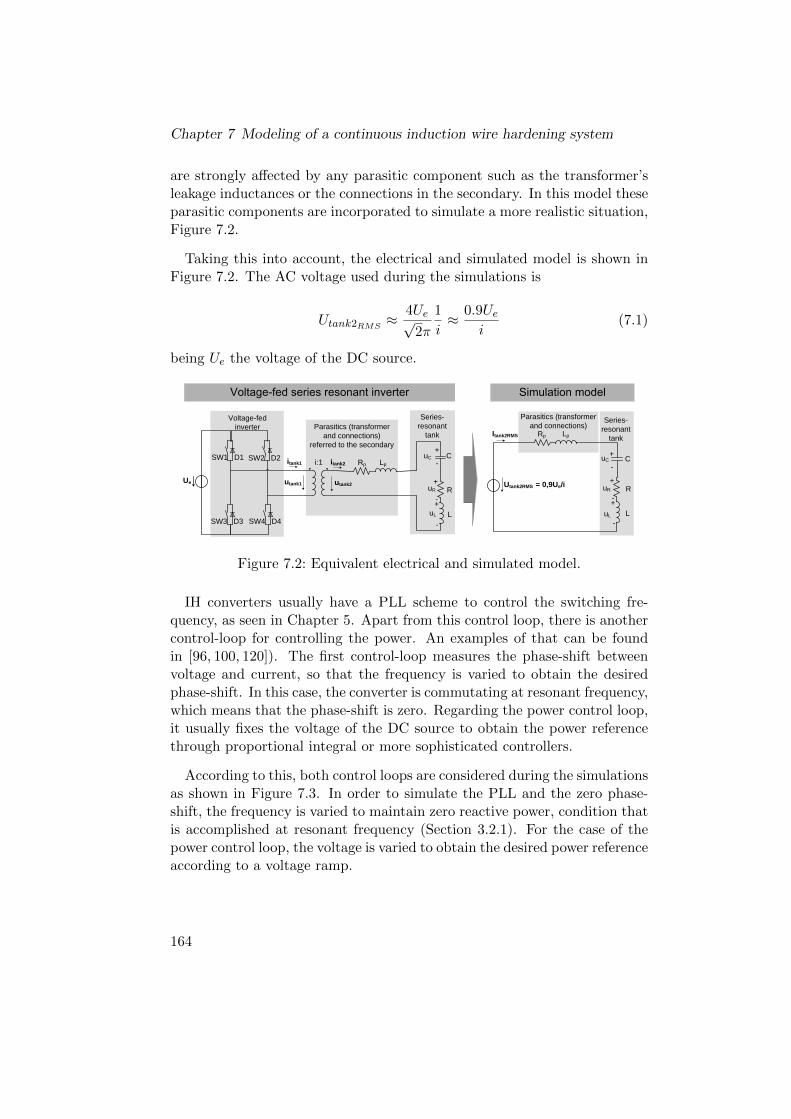
Chapter 7 Modeling of a continuous induction wire hardening system
are strongly affected by any parasitic component such as the transformer’sleakage inductances or the connections in the secondary. In this model theseparasitic components are incorporated to simulate a more realistic situation,Figure 7.2.
Taking this into account, the electrical and simulated model is shown inFigure 7.2. The AC voltage used during the simulations is
Utank2RMS≈ 4Ue√
2π
1
i≈ 0.9Ue
i(7.1)
being Ue the voltage of the DC source.
Parasitics (transformer and connections)
referred to the secondary
utank1
itank1
Ue
R
L
C+
-
+
+-
-
Voltage-fed inverter
uC
uR
uL
SW3 SW4
SW2D1
D3
D2
D4
SW1
R
L
CuC+
-
+
+-
-
uR
uL
i:1
utank2
itank2
Series-resonant
tank
Utank2RMS = 0,9Ue/i
Itank2RMS
Series-resonant
tankRp Lp
Parasitics (transformer and connections)
Rp Lp
Figure 7.2: Equivalent electrical and simulated model.
IH converters usually have a PLL scheme to control the switching fre-quency, as seen in Chapter 5. Apart from this control loop, there is anothercontrol-loop for controlling the power. An examples of that can be foundin [96, 100, 120]). The first control-loop measures the phase-shift betweenvoltage and current, so that the frequency is varied to obtain the desiredphase-shift. In this case, the converter is commutating at resonant frequency,which means that the phase-shift is zero. Regarding the power control loop,it usually fixes the voltage of the DC source to obtain the power referencethrough proportional integral or more sophisticated controllers.
According to this, both control loops are considered during the simulationsas shown in Figure 7.3. In order to simulate the PLL and the zero phase-shift, the frequency is varied to maintain zero reactive power, condition thatis accomplished at resonant frequency (Section 3.2.1). For the case of thepower control loop, the voltage is varied to obtain the desired power referenceaccording to a voltage ramp.
164

ii
“PhD” — 2012/5/21 — 8:58 — page 165 — #101 ii
ii
ii
7.4 Numerical analysis considering the converter’s performance
φshift(measured)
PI Switchingfrequency
φshift* +
P(measured)
PI+ UeP*
(ramp)
Reactive power equal to zero
Voltage varied according to a voltage
ramp to reach the power reference
Figure 7.3: Converter control loops and simulated model.
7.4.2 Load modeling
Due to its length and complexity, the electromagnetic and thermal problemis out of the scope of this study. In this Section, just a brief summary ofthe equations involved is presented. However, a short overview of nume-rical methods applied to IH and a first bibliography of the equations andassumptions done can be found in Section 2.3.
During this study, there was a research of the different methods and soft-wares that could perform this simulation. After analyzing and using differentcommercial softwares, Flux2D c© was chosen because allows the coupling ofthe electromagnetic-thermal and kinematic problems and permits varyingthe voltage and frequency during the process. It has to be noted, that thereare other softwares that could have also been used.
Numerical simulation of IH systems requires a coupled magnetic and ther-mal model due to the temperature dependence of the material’s properties.In case of Flux2D c©, the equations are solved using FEM (see Section 2.3.2)with an indirect coupling (see Section 2.3.3).
Considering the definitions of magnetic vector potential
B = ∇×A (7.2)
and electric scalar potential
Js = −σ∇φ (7.3)
165

Chapter 7 Modeling of a continuous induction wire hardening system
with Js being the source (excitation) current density and σ the electricalconductivity. Integrating in space the Faraday-Lenz law (Equation 2.10),the electric field strength E is equal to
E = −∂A∂t−∇φ (7.4)
Considering that the current desity J is related to the electrical fieldstrength E by the conductivity and using Equation 7.4
J = σE = −σ∂A∂t− σ∇φ = Je + Js (7.5)
where the first of the terms, −σ ∂A∂t , represents the eddy currents (Je) andthe second the source currents, (Js).
Joining Equation 2.14 with 7.5
∇×H = J = −σ∂A∂t− σ∇φ (7.6)
that combined with
B = µH (7.7)
and with the definitions of magnetic vector potential and electric scalarpotential (Equations 7.2 and 7.3), becomes
∇×(
1
µ∇×A
)+ σ
∂A
∂t= Js (7.8)
where A is the magnetic vector potential, Js is the excitation current densitysource, µ is the magnetic permeability of the material and σ its electricalconductivity.
Assuming that
∇× (∇×A) = ∇ (∇ ·A)−∇2A (7.9)
and the mathematical definition of vector potential (from Equations 2.13and 7.2)
∇ ·B = ∇ · (∇×A) = 0 (7.10)
Therefore, considering µ linear, Equation 7.8 becomes
166

ii
“PhD” — 2012/5/21 — 8:58 — page 167 — #102 ii
ii
ii
7.4 Numerical analysis considering the converter’s performance
1
µ∇2A− σ∂A
∂t= −Js (7.11)
Due to the symmetries in the geometry of the system, this equation canbe expressed in cylindrical coordinates with the complex vector A beingindependent of the azimuth angle (A(r,z)). In this case, the problem isaxisymmetric and H has two components in the space, whereas E just one [7,p. 468]. Considering that the variables are sinusoidal time-varying, they areexpressed using their complex images (Section 2.3.1). Thus, Equation 7.11is expressed as
∂
∂r
(1
µr
∂
∂r(Ar)
)+
∂
∂z
(1
µ
∂A
∂z
)− jωσA = −Js (7.12)
where ω is the angular frequency of A. This equation is solved by the pro-gram and the heat produced by the eddy currents is computed with
pv =|j$σA|2
2σ(7.13)
where pv is the induced power density.
Then, this heat increases the temperature following the Fourier equation
ρmcp∂T (r, z, t)
∂t−∇ (k∇T (r, z, t)) = pv(r, z, t) (7.14)
where T is the temperature value, k is the thermal conductivity, cp is thespecific heat and ρm is the mass density.
With regards to the movement of the wire, the displacement is consideredduring the thermal field computation. The method utilized by Flux2D c©
during the simulations is the translating air-gap technique, using the step bystep method explained in [121]. The currents induced by the displacementof the wire are not considered because the velocities are low.
7.4.3 Solving procedure combining converter and load modelling
With reference to the problem of the interdependence between converterand load, the frequency and the voltage of the source are modified in theelectromagnetic and thermal problem. The source’s frequency is set equalto the resonant frequency of the load and the voltage is varied manuallyaccording to the power control-loop presented in Figure 7.3.
167
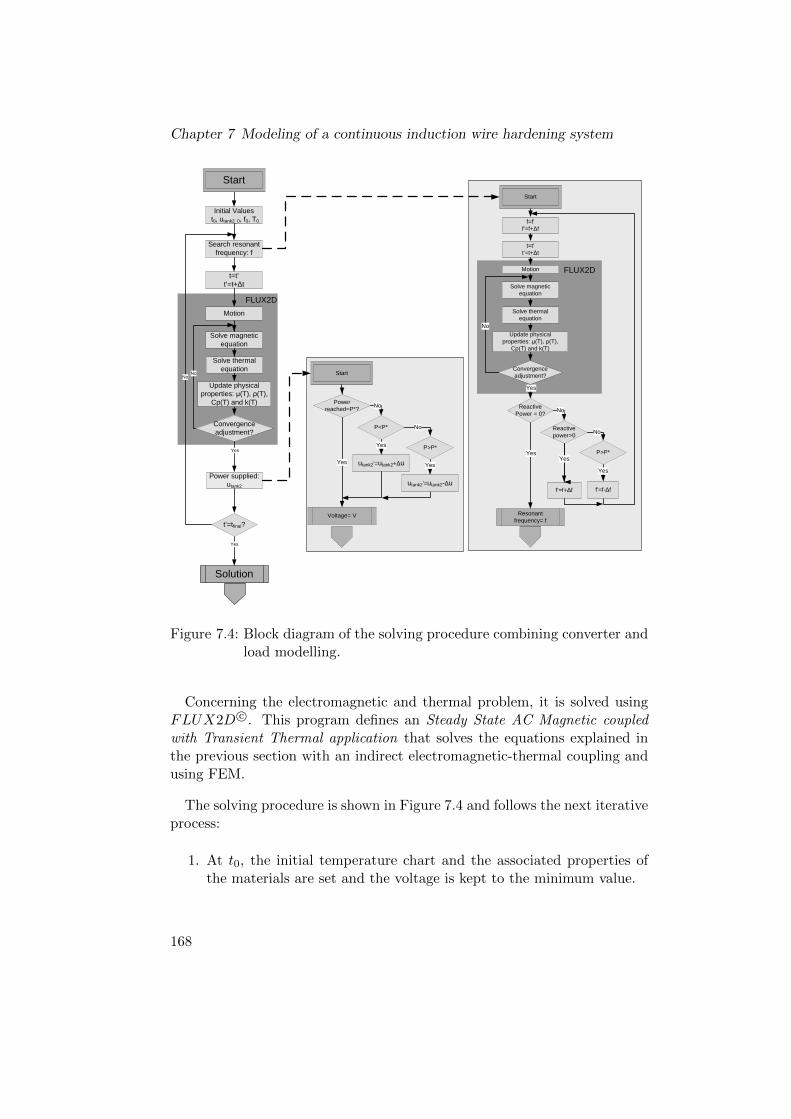
Chapter 7 Modeling of a continuous induction wire hardening system
Initial Valuest0, utank2_0, f0, T0
Solve magnetic equation
Convergence adjustment?
Start
Solve thermal equation
Update physical properties: μ(T), ρ(T),
Cp(T) and k(T)
t=t’t’=t+∆t
No
Search resonant frequency: f
Solve magnetic equation
Convergence adjustment?
Solve thermal equation
Update physical properties: μ(T), ρ(T),
Cp(T) and k(T)
t=t’t’=t+∆t
No
Yes
ReactivePower = 0?
f=f’f’=f+∆f
Resonant frequency= f
Yes
Solution
Yes
Yes
Power supplied: utank2
Start
Start
Power reached=P*?
P<P*
No
utank2’=utank2+∆u
P>P*
No
Yes
Yes
Voltage= V
Yes
t’=tfinal?
No
FLUX2D
Reactive power>0
No
f’=f+∆f
P>P*
f’=f-∆f
No
Yes
utank2’=utank2-∆u
Yes
Yes
Motion
Motion FLUX2D
Figure 7.4: Block diagram of the solving procedure combining converter andload modelling.
Concerning the electromagnetic and thermal problem, it is solved usingFLUX2D c©. This program defines an Steady State AC Magnetic coupledwith Transient Thermal application that solves the equations explained inthe previous section with an indirect electromagnetic-thermal coupling andusing FEM.
The solving procedure is shown in Figure 7.4 and follows the next iterativeprocess:
1. At t0, the initial temperature chart and the associated properties ofthe materials are set and the voltage is kept to the minimum value.
168

ii
“PhD” — 2012/5/21 — 8:58 — page 169 — #103 ii
ii
ii
7.5 Simulations
2. Afterwards, the resonant frequency is searched for the initial tempera-ture by maintaining the reactive power equal to zero. The next timestep t1 is computed.
3. Then, the magnetic and electrical properties are evaluated for the ini-tial temperature and the magnetic problem is solved, obtaining thetransferred power.
4. The temperature chart is calculated for t1 and the new properties ofthe material are found.
5. At this moment, the magnetic and electric properties are evaluatedagain for the new temperature chart with the new material properties.Then, the thermal problem is solved again, obtaining a second tempe-rature chart. If the difference between both temperature distributionsis smaller than a certain error, the solution is validated and the nexttime step computed. Otherwise the iterations continue until the errordiminishes and the solution can be validated for t1.
6. Once the convergence is reached for t1, the voltage is modified accord-ing to the desired power by increasing the voltage with a 100 V/s rampand limited to 245 V.
7. The resonant frequency is searched again and the next time step t2 iscomputed.
8. The process continues until the end of the heating process at tfinal.
7.5 Simulations
Following the considerations of Section 7.4, a Post-Curie equipment in thetransition between 720 C and 800 C is simulated. First, the model isdescribed in Section 7.5.1, explaining the geometrical and physical charac-teristics. And afterwards, three cases are simulated to compare the results ofthe solving procedure with classical approaches. This is explained in Section7.5.2.
7.5.1 Simulated model
The system modeled is a 177 kHz and 4 kW system for continuous steel wirehardening. It is composed of 6 inductors of 10 square-shape turns that areheating a 3 mm diameter wire of AISI 1080 steel, with the characteristics
169

Chapter 7 Modeling of a continuous induction wire hardening system
seen in Tables 7.1 and 7.2. The coils are connected in pairs and series formingthree tanks connected in parallel, and the capacitors, as well as the parasiticcomponents, are connected in series. In Figure 7.5, the connections of theelectrical circuit are shown, with each turn being modeled by a two terminalsolid conductor. In Figure 7.6 a coil and the wire model are shown.
Table 7.1: Parameters of the tank.
Parameter Value
Number of coils 6Number of turns 10Inner diameter 20 mm
Coil Outer diameter 32 mmturn’s width 1 mmSpace between turns 1 mmSpace between coils 36 mm
Capacitor Capacitance 1.6 µFParasitic Resistance 10 mΩComponents Inductance 150 nH
Wire Diameter 3 mm
Table 7.2: AISI 1080 characteristics.
Temperature Resistivity Relative Specific ThermalC mΩmm permeability heat conductivity
kJ/(m3C) W/(mC)
0 0.180 100 3790 47.820 0.180 100 3790 47.8100 0.232 100 3850 48.1200 0.308 100 4140 45.2300 0.410 100 4400 41.3400 0.505 40 4700 38.1600 0.772 40 5470 32.7700 0,932 30 5890 30.1750 1.032 5 15900 30.1800 1.129 1 4690 24.4900 1.164 1 4690 24.4951 1.164 1 4690 24.41100 1.164 1 4690 24.4
In this case, the wire length is chosen 2350 mm because it allows a simula-tion of more than 15 s ensuring that the wire is crossing all the coils duringthe whole simulation. Thus, the model requires a huge dimension comparedto the area of interest, which is just the wire and the area near the coils. Forproviding an accurate mesh and avoid long computation times, the penetra-tion depth has been calculated to increase the mesh in this area (see Figure7.7). During the construction of the mesh, a first set of simulations have
170

ii
“PhD” — 2012/5/21 — 8:58 — page 171 — #104 ii
ii
ii
7.5 Simulations
been done to ensure the convergence of the results.
Series-resonant tankParasitics
utank2
Coil
Turn
Figure 7.5: Electrical circuit simulated.
Coil
Turn
Wire
Compressible area (radius
2.25 mm)
Figure 7.6: A coil and the wiremodeled.
Coil 1Coil 2Coil 3Coil 4Coil 5Coil 6
radius = 2300 mm
radius = 2700 mm
wire of length 2350 mm
wire’s movement
end of compressible area ( ± 2100 mm)
Figure 7.7: Meshing of the system.
Flux2D c© requires of the definition of a compressible area where the trans-lation takes place. In this case, the compressible area is formed by a squareof 4200 mm per 2.25 mm, as shown in Figures 7.6 and 7.7. The infinite boxused by Flux2D c© to model an infinite domain is defined by half semicircleof 2300 mm inner radius and 2700 mm external radius.
In the external radius of the wire, a convection boundary condition with an
171

Chapter 7 Modeling of a continuous induction wire hardening system
emissivity of 0.8 and a heat transfer coefficient of 20 W/(m2C) is imposed.The velocity of the wire is set to 5 m/min, the temperature of the air at 40C and the initial temperature of the wire at 720 C.
7.5.2 Simulation results
In order to illustrate the importance of considering the converter’s behaviorduring the simulations, three cases have been simulated:
• Case 1: The voltage and the frequency are constant during the wholeprocess, and the frequency is set to the initial resonant frequency ofthe process.
• Case 2: Equal to Case 1 but the frequency is set to the final resonantfrequency of the process.
• Case 3: The voltage and frequency is varied according to the controlshown in Figure 7.4 with a power reference set to 3.5 kW and a 100V/s voltage ramp with a limit of 245 V.
The first and the second case represent the modeling following the e-lectromagnetic-thermal approach explained in Section 7.3. In these cases,the voltage and frequency of the source is constant, whereas in the thirdcase, which is the method presented in Section 7.4, both parameters varyconsidering the converter’s performance.
Taking this into consideration, the active power, reactive power, voltage,current and frequency of the converter for Cases 1, 2 and 3 are plottedin Figures 7.8 and 7.9. The voltage value Ue, in Figure 7.9, is calculatedwith Utank2RMS
obtained from Flux2D c© and according to Equation 7.1.The value of current Itank1RMS
represents the current in the primary of thetransformer, as seen in Figure 7.2. This value is the RMS value calcu-lated with Itank2RMS
and using the transformer’s transformation ratio (i).The equivalent impedance (inductance plus resistance) of the inductor-workpiece and the resonant frequency is plotted in Figure 7.10. Afterwards, thetemperature profile for different central points of the wire for the three casesis shown in Figure 7.11.
In Case 1, the reactive power at the beginning is zero because the converteris switching at the resonant frequency. When the temperature of the wireincreases, the inductance value decreases due to the variation in the wire’sproperties and, as a result, the resonant frequency increases, as shown inFigure 7.10. In this case, the switching frequency is constant, thus, when
172

ii
“PhD” — 2012/5/21 — 8:58 — page 173 — #105 ii
ii
ii
7.5 Simulations
0 5 10 150
1000
2000
3000
4000
P (
W)
Active power of the converter
Case 1Case 2Case 3
0 5 10 15-1500
-1000
-500
0
500
1000
Q (
var)
time (s)
Reactive power of the converter
Case 1Case 2Case 3
Figure 7.8: Active and reactive power of the converter in Cases 1, 2 and 3.
0 5 10 150
100
200
300
Ue (
VD
C)
Voltage of the DC source (Ue)
Case 1Case 2Case 3
0 5 10 150
10
20
30
I tank
1 (A
rms)
Current of the converter (Itank1
)
Case 1Case 2Case 3
0 5 10 15176
178
180
182
f (kH
z)
time (s)
Switching frequency
Case 1Case 2Case 3
Figure 7.9: DC voltage, RMS current and switching frequency of the con-verter in Cases 1, 2 and 3.
173

Chapter 7 Modeling of a continuous induction wire hardening system
0 5 10 1510
20
30
40
R (
m
)
Equivalent resistance of the inductor-work piece
Case 1Case 2Case 3
0 5 10 150.33
0.34
0.35
0.36
L (
H)
Equivalent inductance of the inductor-work piece
Case 1Case 2Case 3
0 5 10 15177
178
179
180
181
f reso
nant
(kH
z)
time (s)
Resonant frequency of the whole equivalent circuit
Case 1Case 2Case 3
Figure 7.10: Equivalent impedance of inductor-workpiece and resonant fre-quency for Cases 1, 2 and 3.
0 5 10 15720
740
760
780
800
T (
ºC)
Temperature in the center of the wire: Case 1
z=-300z=-400z=-500z=-600z=-700z=-800z=-900
0 5 10 15720
740
760
780
800
T (
ºC)
Temperature in the center of the wire: Case 2
z=-300z=-400z=-500z=-600z=-700z=-800z=-900
0 5 10 15720
740
760
780
800
T (
ºC)
time (s)
Temperature in the center of the wire: Case 3
z=-300z=-400z=-500z=-600z=-700z=-800z=-900
Figure 7.11: Temperature profile for wire’s central points in Cases 1, 2 and3.
174

ii
“PhD” — 2012/5/21 — 8:58 — page 175 — #106 ii
ii
ii
7.5 Simulations
the resonant frequency varies, the converter provides reactive power thatdoes not generate heat (Figure 7.8). This is specially noticed at the end ofthe process, when switching and resonant frequency are most different.
In Case 2, the reactive power at the beginning is not zero, because theswitching frequency of the converter is set to the final resonant frequency ofthe process. However, the reactive power becomes zero as the wire temper-ature increases and the resonant frequency is reached, as shown in Figures7.8 and 7.10. Contrary to the previous case, at the beginning there is a partof reactive power that does not produce heat.
In Case 3, the voltage is varied according to a voltage ramp of 100 V/sfollowing a power control-loop set to 3,5 kW and the converter is switching atthe resonant frequency (Figures 7.8 and 7.9). In this case, the reactive poweris zero during the whole process and all the available power of the converter isused to heat (Figure 7.8). At the beginning, the voltage is zero and increasesuntil the power reference is reached. In this situation, the wire is colder andits equivalent resistance and inductance are higher. As the temperature ofthe wire increases, its equivalent resistance and inductance values decrease,as can be observed in Figure 7.10. Thus, the current value increases and thecontrol decreases the voltage to maintain the power reference.
Regarding the temperature for different moving central points of the wirein Figure 7.11, the decrease of temperature due to the space between thesix coils that the wire crosses can be observed. It can also be observed thatthe temperature reached in Cases 2 and 3 is slightly higher than in Case 1.The reason is that the active power applied to the wire is higher in Cases2 and 3. It is also shown that in Case 3 the wire starts to increase thetemperature about 2 seconds later. This is due to the voltage value, whichis lower than in the other cases. However, the steady-state is reached earlier,in 6 - 7 seconds approximately. Observing Case 2, the final temperature issimilar to Case 3, but the steady-state is reached 3 seconds afterwards. Thereason is that in Case 2, at the beginning, the source is out of the resonantfrequency and only a part of the power is used to heat the wire. In this case,the dynamics depend on the time that the wire takes to be heated and thishappens when the resonant frequency equals to the switching frequency andprovides the 3.5 kW.
Observing more in detail Figure 7.9 for Case 3, the steady-state is reachedat 6 - 7 seconds. Considering that the sum of the 6 coils length is approxi-mately 0.6 m and the wire is moving at 5 m/min, the steady-state is reachedwhen the wire has crossed the six coils, at approximately 7 seconds. In case
175

Chapter 7 Modeling of a continuous induction wire hardening system
3, the converter dynamics is faster and reaches the power reference beforethe wire has crossed the coils, as seen in Figure 7.8. But, in case of loadsthat moved faster, the process could arrive to be determined by the con-verter’s performance. Moreover, in case 3 the voltage does not reach themaximum value, set to 245 V, it just arrives to a smaller peak and dimin-ishes afterwards. In case of having a greater impedance, for example witha colder wire, these peak could increase, arriving to the maximum value of245 V. Under these circumstances, the dynamics of the process would bealso conditioned by the converter’s performance.
7.6 Experimental results
Experimental tests have been performed with an industrial equipment de-signed and constructed by the authors of this thesis and shown in Figure7.12. The inductors and workpieces have the same geometric and physicalcharacteristics than the simulated model. The wire arrives to the first ofthe 6 coils from a previous heating stage at 720 C and the converter heatesit up to the Curie temperature. The three cases simulated in the previoussection have been implemented, focusing on the case where the voltage andfrequency vary (Case 3).
Figure 7.12: Experimental setup used to test the proposed control method.
During the first experimentation, the voltage and frequency were fixedas in Case 1 (constant voltage and frequency set at the initial resonant
176

ii
“PhD” — 2012/5/21 — 8:58 — page 177 — #107 ii
ii
ii
7.6 Experimental results
frequency). In this case, the converter spent from 5 to 10 seconds more thanin the simulations to reach the steady-state. Moreover, it was observed thatin case of decreasing the temperature at which the wire enters the inductors,the converter could not heat the wire. The reason was that the impedanceof the load was too high and, thus, the current and the power were limited.To give power to the wire, the voltage had to be higher and the convertercould not reach it.
In the second experimentation, the voltage and frequency was set like inCase 2 (constant voltage and frequency set at the final resonant frequency).Under these circumstances, the converter always reached the steady-statespending less time to heat the wire than in Case 1. In this case, the finaltemperature was approximately 10 to 20 C higher than in the previouscase. However, the converter took more than twice longer than within theconverter in normal operation, that is when the voltage and frequency varyduring the whole process.
In the third experimentation, the converter was working in normal opera-tion. The voltage varied according to a power control-loop and following theresonant frequency, similar to Case 3 in the simulations. For this situation,the voltage and the current in the primary and secondary are shown inFigures 7.13, 7.14, 7.15 and 7.16.
To compare these figures with Figure 7.9, some considerations have tobe taken. First, the voltage and currents are plotted as a function of time,whereas in Figure 7.9 the RMS value of the current in the complex formand the value of the voltage DC source are represented. Although theyare graphically different, the comparison of both figures is possible as thetendency of the system can be observed. Secondly, in these figures the highpart of the square-wave corresponds to the DC value of the source. In caseof the current, the maximum is proportional to the RMS value and gives anidea of the value as well as its behavior.
Considering this, in Figure 7.13, the voltage increased reaching the maxi-mum value in approximately 3.5 seconds and afterwards decreased slowly.Comparing with the simulations in Figure 7.9, at the beginning the voltagehas more than one slope. In this case, there is a first and fast increase duringapproximately 0.5 seconds and afterwards a softer increase. The reason forthis difference between simulation and experimental results is that real IHconverters need an initial voltage to start working. This initial voltage helpsthe converter to measure the current’s zero-crossing and detect the resonantfrequency of the tank. Thus, the voltage at the output has to be highenough to have an appropriate current waveform. Otherwise, the current is
177
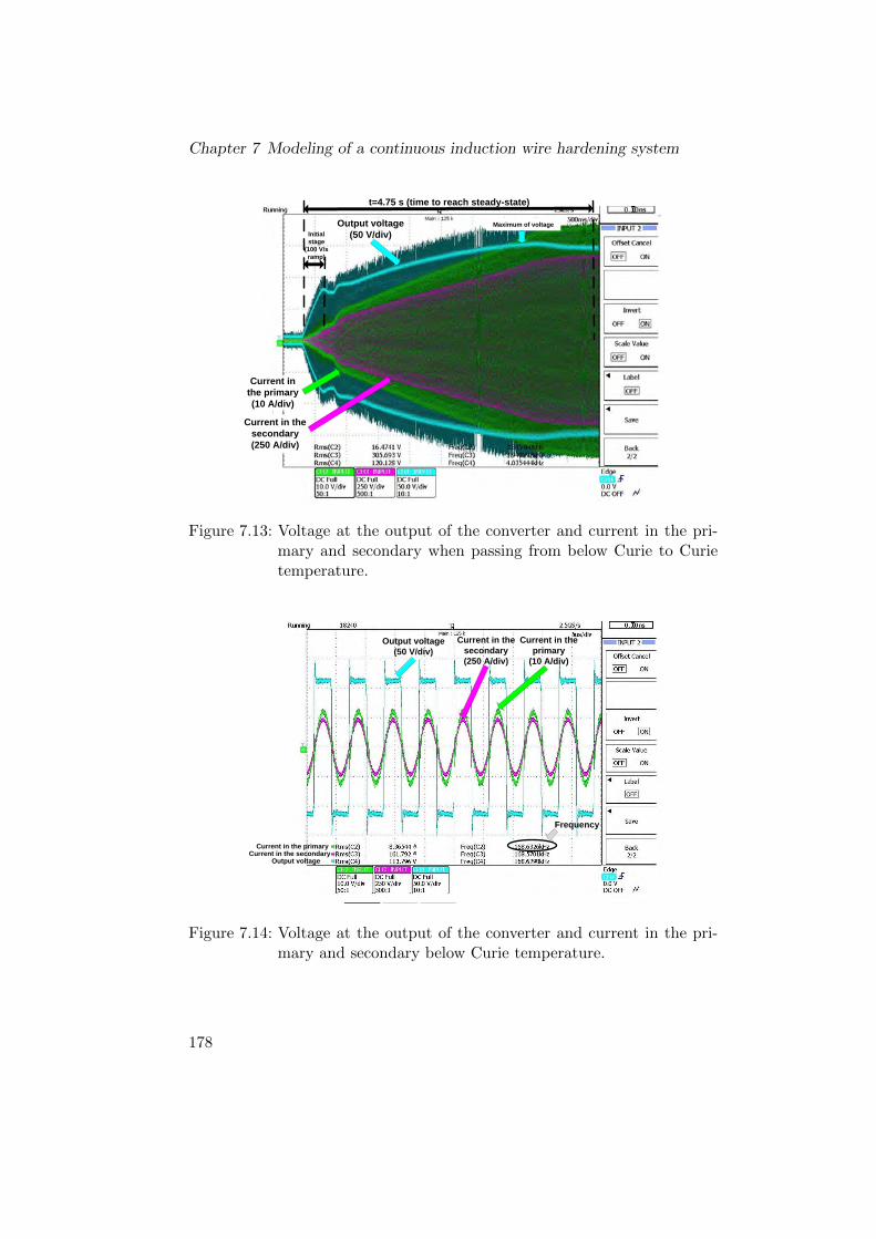
Chapter 7 Modeling of a continuous induction wire hardening system
Output voltage (50 V/div)
Current in the primary(10 A/div)
Current in the secondary (250 A/div)
t=4.75 s (time to reach steady-state)
Initial stage
(100 V/s ramp)
Maximum of voltage
Figure 7.13: Voltage at the output of the converter and current in the pri-mary and secondary when passing from below Curie to Curietemperature.
Current in the secondary(250 A/div)
Current in the primary
(10 A/div)
Frequency
Output voltage(50 V/div)
A
A
Output voltage
Current in the primaryCurrent in the secondary
Figure 7.14: Voltage at the output of the converter and current in the pri-mary and secondary below Curie temperature.
178

ii
“PhD” — 2012/5/21 — 8:58 — page 179 — #108 ii
ii
ii
7.6 Experimental results
Frequency
Output voltage
Current in the primaryAA
Current in the secondary
Current in the secondary(250 A/div)
Current in the primary
(10 A/div)
Output voltage(50 V/div)
Figure 7.15: Voltage at the output of the converter and current in the pri-mary and secondary at Curie temperature.
t=4.5 s (time to reach steady-state)
Output voltage (50 V/div)
Current in the primary(10 A/div)
Current in the secondary (250 A/div)
Initial stage
(100 V/s ramp)
Maximum of voltage
Figure 7.16: Voltage at the output of the converter and current in the pri-mary and secondary when passing from below Curie to Curietemperature for a lower power.
179

Chapter 7 Modeling of a continuous induction wire hardening system
too small and leads to false zero-crossings, disabling the proper control ofthe converter. Therefore, at the beginning the control increases the voltageautomatically with a 100 V/s ramp until the voltage reaches 80 V and thecurrent is high enough. Once the system detects that is switching at theresonant frequency because the phase-shift is zero, the power control-loopstarts working. In this case, the power control-loop was a PI controller witha lower dynamic response than the 100 V/s voltage ramp supposed duringthe simulations. This is the reason why this second slope is lower than theone in the simulations.
Regarding the thermal behavior, the temperature of the wire was 720 Cwhen reaching the inductors and oscillated between 790 C and 810 C atthe end.
Figures 7.14 and 7.15 are a zoom of the voltage and the currents duringthe transition stage. It is observed that the first harmonic approximationdone in Section 7.4.1 is correct because the current is perfectly sinusoidal.It can also be observed that the frequency varied from 168 kHz to 170 kHz,which are similar values to the ones obtained during the simulations. It is asmall variation because the parasitic components do not vary much duringthe heating process, since the transformer and connections are water cooled.In further investigations, the parasitic components should be reduced byshortening and paralleling these transformer secondary connections. Never-theless, in this type of systems the parasitic components should be consid-ered. In Figures 7.14 and 7.15, it is also observed that the assumption ofneglecting the dead-time during the simulations is accurate.
Figure 7.16 shows the same parameter than Figure 7.13 but with a lowerpower reference. The aim of this test was to show that the dynamics ofthe process was dependant on the wire’s velocity. In both cases the voltageincreased until the power was reached. Afterwards, the current increasedand the voltage decreased to maintain the power reference. In Figure 7.13the steady-state was reached in approximately 4.75 seconds and in Figure7.16 at 4.5 seconds, which corresponds to the time spent in crossing the coils.In the real case, the distance between coils was lower than in the simulationsand, thus, the time spent in crossing them was also lower (approximately 5seconds). Therefore, in both cases the dynamics of the process was affectedby the velocity of the wire. Moreover, in the first case the maximum voltagewas reached at 3.5 seconds and in the second case at only 2 seconds. Inboth cases the voltage reference was low enough and the converter dynamicsfast enough for following it. However, in case of the converters with lower
180

ii
“PhD” — 2012/5/21 — 8:58 — page 181 — #109 ii
ii
ii
7.7 Summary
dynamics or processes with higher velocities, the time to reach the steadystate could be conditioned by the converter.
Some of the differences between the simulated and the experimental resultsare obviously conditioned by the intrinsic differences between the geometriesof the pieces, the properties of the heated material and the assumptions madeduring the modeling. Nevertheless, most of the differences are due to thedifficulty of determining the parasitic components and the complexity ofsimulating the control system of a real converter. Taking these differencesinto account, the results provided for Case 3 show a correspondence with thereal system behavior. The results illustrate the importance of considering theoperation and dynamics of the converter during IH simulations, especiallyin cases where there is a great change in load properties.
7.7 Summary
In this Chapter, an industrial process of continuous hardening and temper-ing of steel wires has been explained. During this process, the wire needs tobe heated above its Curie temperature. At this temperature the steel be-comes non-magnetic and there is a great change in the wire’s properties thataffect the design and the control of the converter. Studying and modelingthis situation is interesting because of this change and the high interactionbetween the electrical and electromagnetic-thermal problems.
The difficulty of modeling IH systems and the interdependence betweenconverter and load is introduced, explaining two different approaches: theelectrical and the electromagnetic-thermal approach. The first one is mainlyused by converter designers and is based on the supposition that the inductor-workpiece equivalent impedance does not vary, but the source parametersdoes. Contrarily to this approach, the electromagnetic-thermal approachsupposes that the source parameters remain constant, whereas the loadvaries during the process. Some attempts have been done to combine bothapproaches, but in none of them the control of the converter and its basicoperation are described and experimental results provided.
In order to overcome the mutual influence between the converter and theload, a simple method of simulating IH systems using FEM is presented.The topology of the converter and its operation is explained, assuming somesimplifications like neglecting the dead-time or considering just the first har-monic. The parasitic components of the transformer and inductance aretaken into consideration and the control-loops of the converter are explained.
181

Chapter 7 Modeling of a continuous induction wire hardening system
Afterwards, the basic equations of the electromagnetic-thermal problem arepresented and the solving procedure, considering the converter’s operation,is exposed.
The system is simulated with a commercial FEM software (Flux2D c©),modifying the voltage according to a manual power control-loop and settingthe switching frequency to the resonant frequency. In order to compare themethod presented with the classical electromagnetic-thermal approaches,two additional simulations have been done maintaining constant the voltageand the frequency. The three simulated cases are:
• Case 1: The voltage and the frequency are constant during the wholeprocess, and the frequency is set to the initial resonant frequency ofthe process.
• Case 2: Equal to Case 1 but the frequency is set to the final resonantfrequency of the process.
• Case 3: The frequency is varied manually according to a frequencycontrol loops similar to the PLL presented in Chapter 5, in which theconverter commutates at resonant frequency. The power control loopis controlled by varying the voltage of the DC source, similar to theVFSRI converter explained in Chapter 3. The resonant frequency isset during the simulations by maintaining the reactive power to zeroand the power control loop is modeled with a 100 V/s voltage ramplimited to 245 V.
The simulation of these three cases has confirmed the importance of con-sidering the changes in source’s voltage and frequency when simulating IHsystems. In case of varying these parameters, all the power is used to pro-duce heat during the whole process. The final temperature in Cases 2 and 3was higher compared to Case 1 and in Case 3 the steady-state was reachedearlier. During the simulations, the influence of the converter in the dynam-ics of the heating process and the interdependence between the load and theconverter’s behavior was also observed.
Finally, experimental results using an equipment designed and constructedby the authors were presented. Although there are differences between theexperimental and simulation results, these are mainly due to the complexityof the converter control system and the difficulty of determining the para-sitic components. However, the results obtained have proven to be accurateenough and show a correspondence between experimentation and simulation.
182

ii
“PhD” — 2012/5/21 — 8:58 — page 183 — #110 ii
ii
ii
7.7 Summary
Compared to other simulation methods in literature, the solving proce-dure presented considers the converter’s performance and provides a flexiblemethod of modeling the overall system behavior. Moreover, the simulationprocedure presented takes advantage of the flexibility provided by commer-cial softwares and allows an easy and flexible implementation compared toother simulation procedures. Finally, the experimental setup showed a corre-spondence with the results obtained, validating the simplifications assumedduring the process.
183

184

ii
“PhD” — 2012/5/21 — 8:58 — page 185 — #111 ii
ii
ii
Chapter 8
Conclusions
8.1 Contributions
The present thesis has investigated the different converter topologies andstructures used in IH field, focusing on the application of wire heating andproviding an extensive revision on IH converters in Chapter 3.
Considering the different converter topologies used in IH, a multichannelconverter structure is studied for high-power and high-frequency applica-tions. The basic converter topologies and connections are studied with theaim of constructing a converter based on these topologies that can profitthis modularity to reduce the designing time, the production cost and themaintenance. As a result of this work, a multichannel converter has beenstudied, implemented and tested in a prototype in Chapter 4.
The present thesis has also investigated the design of a flexible controlfor IH applications. As a result of this study, a software PLL has beendesigned, implemented and tested in a real industrial application in Chapter5. The main benefit of this software PLL system is that provides a digitalcontrol that minimizes the analog components and avoids variations due topart spread or temperature drift. Moreover, it is very flexible and can beused in many different applications because the variations required for eachparticular case can be implemented by software. Additionally, clears theway to the programming of more complex control algorithms, thanks to thepossibility of changing the variables dynamically.
A load-adaptive PLL has also been studied. This control system providesan optimum commutation sequence that allows soft-switching even whenthe load varies. As a result of this study, a load-adaptive PLL based on thesoftware PLL presented in Chapter 5 has been designed, implemented andtested in a prototype in Chapter 6.
Finally, the present thesis has investigated the different methods of mode-ling IH systems. In Chapters 1 and 2, the basic concepts regarding analytical
185

Chapter 8 Conclusions
and numerical methods applied to IH field are explained and, in Chapter 7,these methods are used to model a continuous induction wire hardeningsystem considering converter’s operation. Compared to other simulationmethods, the solving procedure considers the converter’s performance andprovides a method of modeling the overall system behavior, taking advantageof the flexibility provided by commercial softwares. The system modeled isa real industrial application that has been tested to prove the accuracy ofthe modeling.
The main contributions of this thesis are summarized below:
• Extensive revision of the main converter topologies and their associa-ted tanks used in IH field (Chapter 3).
• Study of a multichannel converter structure for high-power and high-frequency applications. The study of a multichannel structure basedon the combination and connection of basic structures is realized. Thefinal structure is composed of diodes bridge rectifiers and H-bridgeinverters connected in parallel commutating synchronized to increasethe power or alternatively to increase the frequency. This type ofstructure allows to reduce the designing time, the production costsand the maintenance of industrial equipments. A prototype based ontwo H-bridges in parallel for doubling the frequency has been testedshowing good results.
• Design of a software PLL for IH applications. This software PLLis all-digital and software programmed, so that minimizes the need ofanalog components, provides more adaptability to variations and clearsthe way for the programming of more complex control algorithms.The system has been tested in a real industrial application proving itsreliability and flexibility. The contributions are collected in
– [122] G. Martın-Segura, J. Lopez-Mestre, H. Rivas-Guerrero,M. and Teixido-Casas and D. Montesinos-Miracle, ”A low costDSP-based control method for high frequency parallel resonantcurrent-fed inverters”,in Proc. 13th European Conf. Power Elec-tronics and Applications, 2009.
– [123] G. Martın-Segura, P. Sala-Perez, C. Ferrater-Simon, J.Lopez-Mestre, D. Montesinos-Miracle and J. Bergas-Jane, ”All-digital DSP-based phase-locked loop for induction heating appli-cations”, Accepted in European Transactions on Electrical Power,2012.
186

ii
“PhD” — 2012/5/21 — 8:58 — page 187 — #112 ii
ii
ii
8.2 Future work
• Design of a load-adaptive PLL for IH applications. This PLL adaptsthe phase-shift and dead-time to have soft-switching according to theload requirements. The control system has been tested in a prototypeproviding good results. The contributions are collected in
– [124] G. Martın-Segura, C. Ferrater-Simon, J. Lopez-Mestre,G. Gross and D. Montesinos-Miracle, ”Load-adaptive phase-shiftand dead-time control for induction heating applications”, Sub-mitted to European Transactions on Electrical Power, 2012.
• Numerical modeling of a continuous induction wire hardening systemconsidering converter’s operation. A real industrial process has beenmodeled with numerical methods incorporating converter’s behavior.The results obtained in the simulations and those obtained in a real in-dustrial process are compared, showing its correspondence. The maincontributions are collected in
– [125] G. Martın-Segura, C. Ferrater-Simon, D. Montesinos-Miracle,F. Leach and I. Vadan, ”FEM modeling of a continuous induc-tion heating process of steel wire hardening”, in SimpozionuluiNational de Electrotehnica Teoretica, 2010.
– [126] G. Martın-Segura, C. Ferrater-Simon, J. Lopez-Mestre, D.Montesinos-Miracle and J. Bergas-Jane, ”Simulation of an induc-tion hardening system during Curie temperature transition con-sidering converter’s performance”, accepted in COMPEL, 2012.
– [127] G. Martın-Segura, P. Sala-Perez, C. Ferrater-Simon, J.Lopez-Mestre and D. Montesinos-Miracle, ”Study of the parasiticinductance and resistance in continuous wire induction heatingsystems above Curie temperature”, to be submitted.
8.2 Future work
There are still many interesting and challenging fields related to the presentthesis that can be investigated. Some of the possible studies that can bedeveloped are the following:
• A multichannel converter with two H-bridges has been designed andtested in this thesis. The use of fast IGBTs, specific for IH appli-cations, and the parallelization of more H-bridges can improve theconverter’s performance. Furthermore, the automatic change of com-mutation technique or the automatic disconnection of H-bridges can
187

Chapter 8 Conclusions
provide more adaptability and flexibility to the load requirements.Therefore, an interesting research topic is the design of a multichannelconverter with IGBTs commutating over 300 kHz and with an au-tomatic change of commutation technique to have high-power at lowfrequency (inverters commutating synchronized) and high-frequencyat low power (inverters commutating alternatively). This system hasto be able to disconnect some of the inverters in case that the loadrequires low-power and low-frequency, allowing the operation in caseof an H-bridge’s failure.
• During the revision of the different converter topologies used in IH, thebenefits in terms of efficiency improvement and cost reduction withthe use of PDM techniques has been explained. The multichannelconverter is formed by uncontrolled bridge rectifiers and H-bridges,therefore, the study of the application of PDM power control tech-niques to this converter structure is an interesting matter of research.Even more if considering that the multichannel converter is thoughtfor high-power applications where a 1 % increase in the efficiency canrepresent considerable savings.
• During the implementation of the load-adaptive PLL, it was observedthat the IGBT’s parasitic capacitance value had a complex voltagedependence. In order to analyze the affectation of this dependence inthe control, the modeling of switches including this dependence andthe design of a load-adaptive PLL for VFSRIs incorporating theseconsiderations is interesting.
• In order to ensure soft-switching in VFSRIs, their antiparallel diodeshave to conduct before the switches’ turning-on and the turning-on hasto be realized before the current’s change of polarity. In the presentthesis, the load-adaptive PLL designed uses the phase-shift and thedead-time as a control variables, incorporating a gain in this variablesthat ensure the correct sequence of events. However, the dependenceof the IGBT’s parasitic capacitance on the voltage and the need ofsimplifications in the calculations, increase the inaccuracies of the sys-tem. In this sense, an interesting research topic is the design of aload-adaptive PLL that detects the moment at which the diodes startconducting and imposes that the switches turn-on and the current’schange of polarity are done consecutively.
• In CFPRIs, the optimum phase-shift and over-lapping time depend
188

ii
“PhD” — 2012/5/21 — 8:58 — page 189 — #113 ii
ii
ii
8.2 Future work
on the parasitic inductance, which value is more constant than thesemiconductor’s parasitic capacitance. Therefore, the design and im-plementation of the load-adaptive PLL is an interesting matter of re-search.
• During the numerical modeling of a continuous induction wire harden-ing, the variation of frequency and voltage was manually realized uti-lizing a commercial FEM software. The design of a program linked toa commercial computation program that allows the automatic changeof the resonant frequency and the voltage reference according to theconverter’s control loops is an interesting objective for providing morevelocity and flexibility to the analysis. To have this program linkedwith the simulation programs usually utilized by converter designerswould be interesting to speed up and increase the complexity of thesimulations.
• In the present thesis, the numerical modeling of the system was reali-zed for a process that heats above Curie temperature, temperature atwhich there is a great change in the material’s properties. This greatvariation allows a better evaluation of the interdependence betweenthermal, magnetic and electric variables. However, the modeling of acontinuous wire heating below the Curie temperature with numericalmethods considering converter’s operation is an interesting study. Theaim of this study is to evaluate the effect of considering converter’sperformance during the modeling for this case where the load variationis lower.
• During this thesis, the generation of axial voltage in the wire when itis heated in multi-turn inductor was studied with numerical modeling.However, a deeper study have to be realized to assess the importanceof the frequency and coil distribution on this voltage generation.
189

190

ii
“PhD” — 2012/5/21 — 8:58 — page 191 — #114 ii
ii
ii
Bibliography
[1] S. Zinn and S. L. Semiatin, Elements of Induction Heating - Design,Control, and Applications. ASM International, Electronic Power Re-search Institute, Metals Park, Ohio, USA, 1988. v, ix, 1, 5, 6, 9, 10,11, 160
[2] V. Rudnev, D. Loveless, R. Cook, and M. Black, Handbook of Induc-tion Heating. M. Dekker, New York, USA, 2003. v, ix, 1, 3, 5, 9, 10,11, 12, 13, 23, 25, 29, 81, 160
[3] E. R. Laithwaite, “The influence of michael faraday on power engi-neering,” Power Engineering Journal, vol. 5, no. 5, pp. 209–219, 1991.1
[4] A. Chester and M. Tudbury, Basics of induction heating (Vol. I). JohnF. Rider Publisher, Inc., New York, USA, 1960. 1, 6, 18
[5] E. J. Davies and P. Simpson, Induction Heating Handbook. MCGraw-Hill Book Company, Ltd., London, UK, 1979. 1, 18
[6] E. J. Davies, Conduction and induction Heating. P. Peregrinus, Ltd.,London, U.K., 1990. 1, 14, 18, 20, 22, 205
[7] C. H. Gur and J. Pan, Eds., Handbook of thermal process modeling ofsteels. CRC Press, 2008. 1, 8, 23, 25, 167
[8] V. Esteve, “Influencia de los componentes parasitos en el analisisy diseno inversores resonantes paralelo para aplicaciones de calen-tamiento por induccion,” Ph.D. dissertation, Universitat de Valencia,Spain, 1999. 5, 73, 74, 78, 126, 221
[9] J. Espı, “Inversor resonante de tres elementos L-LC con caracterısticacortocircuitable para aplicaciones de calentamiento por induccion,”Ph.D. dissertation, Universitat de Valencia, Spain, 1998. 5, 7, 9, 75
[10] M. T. Thompson, “Inductance calculation techniques — part ii: Ap-proximations and handbook methods,” Power Control and IntelligentMotion, Dec. 1999. 6
191

Bibliography
[11] H. A. Wheeler, “Formulas for the skin effect,” in Proc. of the I.R.E.,1942, pp. 412–424. 6
[12] J. Lee, S. Lim, K. Nam, and D. Choi, “An optimal selection ofinduction-heater capacitance considering dissipation loss caused byesr,” IEEE Trans. Ind. Appl., vol. 43, pp. 1117–1125, 2007. 6
[13] T. Spencer and alter, “Induction hardening and tempering,” AmericanSociety for Metals, Ohio, USA, 1964. 14
[14] M. Kennedy, S. Akhtar, J. Bakken, and R. Aune, “Review of classicaldesign methods as applied to aluminum billet heating with inductioncoils,” in Proc. EPD Congress, San Diego, USA, 2011, pp. 405–414.18
[15] V. Nemkov, “Role of computer simulation in induction heating tech-nique,” in International Induction Heating Seminar, Padua, Italy,1998. 22
[16] V. S. Nemkov and R.Goldstein, “Computer simulation for fundamentalstudy and practical solutions to induction heating problems,” COM-PEL, vol. 22, pp. 181–191, 2003. 23
[17] R. L. Houghton, “Heat treating technology roadmap update 2006, parti: Process & materials technology,” Heat Treating Progress, vol. 6,2006. 23
[18] G. Pfaffmann, “Heat treating technology roadmap update 2006, partiii: Equipment & hardwards materials technology,” Heat TreatingProgress, vol. 6, 2006. 23
[19] J. Lavers, “State of the art of numerical modeling for induction pro-cesses,” COMPEL, vol. 27, pp. 335–349, 2008. 23
[20] G. Benderskaya, “Numerical methods for transient field-circuit coupledsimulations based on the finite integration technique and a mixed cir-cuit formulation,” Ph.D. dissertation, Technischen Universitat Darm-stadt, 2007. 24
[21] N. Mohan, T. M. Underland, and W. P. Robbins, Power electronics.Converters, Applications and Design, 2nd ed. John Wiley & Sons,Inc., USA, 1995. 29, 30
192

ii
“PhD” — 2012/5/21 — 8:58 — page 193 — #115 ii
ii
ii
Bibliography
[22] O. Lucia, L. Barragan, J. Burdio, O. Jimenez, D. Navarro, and I. Ur-riza, “A versatile power electronics test-bench architecture appliedto domestic induction heating,” IEEE Trans. Ind. Electron., vol. 58,no. 99, p. 998, 2011. 30, 161, 163
[23] B. C. Kuo, Sistemas de control automatico, 7th ed. Prentice-HallHispanoamericana, S.A., Mejico, 1996. 31, 32, 35
[24] Y.-L. Cui, K. He, Z.-W. Fan, and H.-L. Fan, “Study on DSP-basedPLL-controlled superaudio induction heating power supply simula-tion,” in Proc. of Int. Conf. on Machine Learning and Cybernetics,vol. 2, 2005, pp. 1082–1087. 39, 125, 126
[25] E. J. Dede, V. Esteve, J. Garcia, A. E. Navarro, and J. A. Carrasco,“On the design of high frequency series resonant converters for in-duction heating applications,” in Proc. Int. Conf. on Ind. Electronics,Control, and Instrumentation, vol. 2, 1993, pp. 1303–1307. 45
[26] C. Cases, J. Jordan, J. M. Magraner, V. Esteve, E. Dede, E. Sanchis,E. Maset, A. Ferreres, J. B. Ejea, and E. Gumbau, “Characterization ofIGBT devices for use in series resonant inverter for induction heatingapplications,” in Proc. 13th European Conf. Power Electronics andApplications, 2009, pp. 1–8. 45, 52
[27] E. J. Dede, J. Jordan, and V. Esteve, “State-of-the art and futuretrends in transistorised inverters for induction heating applications,”in Proc. 5th IEEE Int. Caracas Conference on Devices, Circuits andSystems, vol. 1, 2004, pp. 204–211. 49, 50
[28] J. Jordan, “Estudio del comportamiento de generadores serie mosfetde alta potencia y frequencia,” Ph.D. dissertation, Universitat de Va-lencia, Spain, 2003. 49, 50, 51, 76, 78, 81, 84, 215
[29] J. Jordan, J. M. Magraner, C. Cases, V. Esteve, E. Dede, E. Sanchis,E. Maset, A. Ferreres, J. B. Ejea, and E. Gumbau, “Turn on switchinglosses analysis for Si and SiC diodes in induction heating inverters,” inProc. 13th European Conf. Power Electronics and Applications, 2009,pp. 1–9. 50, 51, 52
[30] A. Fiel and T. Wu, “MOSFET failure modes in the zero-voltage-switched full-bridge switching mode power supply applications,” inProc. 16th Annual IEEE Applied Power Electronics Conf. and Expo-sition, vol. 2, 2001, pp. 1247–1252. 50, 51
193

Bibliography
[31] L. Saro, K. Dierberger, and R. Redl, “High-voltage mosfet behaviorin soft-switching converters: analysis and reliability improvements,”in Proc. 20th Int. Telecommunications Energy Conf., 1998, pp. 30–40.50, 51
[32] W. Choi and S. Young, “Improving system reliability using FRFET inLLC resonant converters,” in Proc. IEEE Power Electronics SpecialistsConf., 2008, pp. 2346–2351. 50, 51
[33] W.-S. Choi, S. mo Young, and D. wook Kim, “Analysis of MOSFETfailure modes in LLC resonant converter,” in Proc. 31st Int. Telecom-munications Energy Conf., 2009, pp. 1–6. 50, 51
[34] H. Aigner, K. Dierberger, and D. Grafham, “Improving the full-bridgephase-shift ZVT converter for failure-free operation under extremeconditions in welding and similar applications,” in 33rd IEEE IASAnnual Meeting, vol. 2, 1998, pp. 1341–1348. 51
[35] L. Grajales, “Analysis and design of a 500 kHz series resonant inverterfor induction heating aplications,” Ph.D. dissertation, Faculty of theVirginia Polytechnic Institute and State University, Blacksburg, Vir-ginia, USA, November 1995. 51, 81, 143
[36] J. Jordan, V. Esteve, R. Garcia-Gil, E. Sanchis, E. Maset, and E. Dede,“New power MOSFET selection method to avoid failures,” in Proc.19th Annual IEEE Applied Power Electronics Conf. and Exposition,vol. 2, 2004, pp. 1257–1261. 52
[37] J. Jordan, V. Esteve, E. Dede, J. M. Magraner, E. Sanchis, E. Maset,and J. E. Ferreres, “Automated calculation method to determine theoutput power based on the frequency for induction heating IGBT par-allel inverter,” in Proc. IEEE Power Electronics Specialists Conf., 17–21 June 2007, pp. 713–718. 73, 74
[38] J. M. Magraner, J. Jordan, C. Cases, V. Esteve, E. Dede, E. Sanchis,E. Maset, A. Ferreres, J. B. Ejea, and E. Gumbau, “Firing strategyfor bidirectional current switches with unidirectional voltage blockingcapability in induction heating parallel resonant inverters,” in Proc.13th European Conf. Power Electronics and Applications, 2009, pp.1–7. 74
194

ii
“PhD” — 2012/5/21 — 8:58 — page 195 — #116 ii
ii
ii
Bibliography
[39] S. Dieckerhoff, M. J. Ruan, and R. W. De Doncker, “Design of anIGBT-based LCL-resonant inverter for high-frequency induction heat-ing,” in 34th IEEE IAS Annual Meeting, vol. 3, 1999, pp. 2039–2045vol.3. 74, 75
[40] E. J. Dede, J. Jordan, V. Esteve, J. M. Espi, and S. Casan, “Se-ries and parallel resonant inverters for induction heating under short-circuit conditions considering parasitic components,” in Proc. IEEEInt. Conf. on Power Electronics and Drive Systems, vol. 2, 1999, pp.659–662 vol.2. 74, 81
[41] E. J. Dede, J. Jordan, V. Esteve, J. V. Gonzalez, and D. Ramirez,“Design considerations for induction heating current-fed inverters withIGBT’s working at 100 kHz,” in Proc. 8th Annual IEEE Applied PowerElectronics Conf. and Exposition, 1993, pp. 679–685. 74
[42] R. Fuentes, P. Lagos, and J. Estrada, “Self-resonant induction furnacewith IGBT technology,” in Proc. 4th IEEE Conf. Industrial Electronicsand Applications, 2009, pp. 1371–1374. 74
[43] J. M. Espi, E. J. Dede, A. Ferreres, and R. Garcia, “Steady-statefrequency analysis of the LLC resonant inverter for induction heating,”in Proc. 5th IEEE Int. Power Electronics Congress, 1996, pp. 22–28.75
[44] J. M. Espi, A. E. Navarro, J. Maicas, J. Ejea, and S. Casans, “Controlcircuit design of the L-LC resonant inverter for induction heating,” inProc. 31st IEEE Power Electronics Specialists Conf., vol. 3, 2000, pp.1430–1435 vol.3. 75
[45] A. Schonknecht and R. W. De Doncker, “Novel topology for parallelconnection of soft switching, high power, high frequency inverters,” in36th IEEE IAS Annual Meeting, vol. 3, 2001, pp. 1477–1482 vol.3. 75,103
[46] A. Schonknecht and R. W. A. A. De Doncker, “Novel topology for par-allel connection of soft-switching high-power high-frequency inverters,”IEEE Trans. Ind. Appl., vol. 39, no. 2, pp. 550–555, 2003. 75, 103, 161
[47] J. M. Espi Huerta, E. J. Dede Garcia Santamaria, R. Garcia Gil, andJ. Castello Moreno, “Design of the L-LC resonant inverter for induc-tion heating based on its equivalent SRI,” IEEE Trans. Ind. Electron.,vol. 54, no. 6, pp. 3178–3187, 2007. 75, 77, 78, 81
195

Bibliography
[48] H. Fujita and H. Akagi, “Pulse-density-modulated power control of a4 kW, 450 kHz voltage-source inverter for induction melting applica-tions,” IEEE Trans. Ind. Appl., vol. 32, no. 2, pp. 279–286, 1996. 81,82, 83
[49] A. Okuno, H. Kawano, J. Sun, M. Kurokawa, A. Kojina, andM. Nakaoka, “Feasible development of soft-switched sit inverter withload-adaptive frequency-tracking control scheme for induction heat-ing,” IEEE Trans. Ind. Appl., vol. 34, no. 4, pp. 713–718, 1998. 81
[50] E. J. Dede, J. Jordan, V. Esteve, J. M. Espi, and S. Casans, “Be-haviour of series and parallel resonant inverters for induction heatingin short-circuit conditions,” in Proc. 3rd IEEE Int. Power Electronicsand Motion Control Conf., vol. 2, 2000, pp. 645–649 vol.2. 81
[51] A. Jangwanitlert, J. Songboonkaew, W. Thammasiriroj, and J. C.Balda, “Analysis of three-level ZVS PWM inverter for induction heat-ing applications,” in Proc. 5th IEEE Int. Power Electronics and Mo-tion Control Conf., vol. 2, 2006, pp. 1–5. 81, 98
[52] J. M. Ho and M. T. Lee, “A novel PWM inverter control circuitryfor induction heating,” in Proc. 5th IEEE Int. Power ElectronicsCongress, 1996, pp. 113–119. 81
[53] A. R. A. M. Makky, H. Abo-Zied, and F. N. Abdelbar, “Parallel op-eration of IGBTs modular converter system for high power high fre-quency induction heating applications,” in Proc. 12th InternationalMiddle-East Power System Conf., 12–15 March 2008, pp. 577–582.81, 101
[54] N. Yongyuth, P. Viriya, and K. Matsuse, “Analysis of a Full-Bridgeinverter for induction heating using asymmetrical phase-shift controlunder ZVS and NON-ZVS operation,” in Proc. 7th Int. Conf. on PowerElectronics and Drive Systems, 2007, pp. 476–482. 81
[55] C. Chen and J. Zou, “DSP-based high-frequency HVDC source forverifying internal pressure of vacuum chamber,” in Proc. Int. Conf.on Condition Monitoring and Diagnosis, 2008, pp. 850–853. 81
[56] J. Essadaoui, P. Sicard, E. Ngandui, and A. Cheriti, “Power invertercontrol for induction heating by pulse density modulation with im-proved power factor,” in Proc. Canadian Conf. on Electrical and Com-puter Engineering, vol. 1, 2003, pp. 515–520 vol.1. 81, 83
196

ii
“PhD” — 2012/5/21 — 8:58 — page 197 — #117 ii
ii
ii
Bibliography
[57] E. J. Dede, V. Esteve, E. Maset, J. M. Espi, A. E. Navarro, J. A.Carrasco, and E. Sanchis, “Soft switching series resonant converter forinduction heating applications,” in Proc. Int. Conf. on Power Elec-tronics and Drive Systems, 1995, pp. 689–693 vol.2. 81
[58] S. Zerouali, A. Allag, S. M. Mimoune, A. H. Hamida, S. Khanniche,and M. Feliachi, “An adaptive control applied to series resonant in-verter for induction heating,” in Proc. 41st Int. Universities PowerEngineering Conf., vol. 2, 2006, pp. 633–636. 81
[59] M.-P. Chen, J.-K. Chen, K. Murata, M. Nakahara, and K. Harada,“Surge analysis of induction heating power supply with PLL,” IEEETrans. Ind. Appl., vol. 16, no. 5, pp. 702–709, 2001. 81, 125, 126, 143
[60] E. J. Dede, J. Jordan, V. Esteve, and C. Cases, “New investigationson short-circuit behaviour of current-fed inverters for induction tubewelding,” in Proc. 4th IEEE Int. Conf. on Power Electronics and DriveSystems, vol. 2, 2001, pp. 760–763 vol.2. 81
[61] F. P. Dawson and P. Jain, “A comparison of load commutated invertersystems for induction heating and melting applications,” IEEE Trans.Power Electron., vol. 6, no. 3, pp. 430–441, 1991. 81
[62] I. Khan, J. Tapson, and I. de Vries, “An induction furnace employing a100 kHz MOSFET full-bridge current-source load-resonant inverter,”in Proc. IEEE Int. Symposium on Industrial Electronics, vol. 2, 1998,pp. 530–534 vol.2. 81
[63] Z. Zhao, Y. Peng, and Y. Li, “Devices dissipation of series-resonantinverter under pulse-width phase-shift operating mode,” in Proc. Asia-Pacific Power and Energy Engineering Conf., 2010, pp. 1–4. 83
[64] L. Grajales, J. A. Sabate, K. R. Wang, W. A. Tabisz, and F. C. Lee,“Design of a 10 kW, 500 kHz phase-shift controlled series-resonantinverter for induction heating,” in Proc. IEEE Industry ApplicationsSociety, 1993, pp. 843–849. 83, 143
[65] V. Esteve, E. Sanchis-Kilders, J. Jordan, E. J. Dede, C. Cases,E. Maset, J. B. Ejea, and A. Ferreres, “Improving the efficiency ofIGBT series-resonant inverters using pulse density modulation,” IEEETrans. Ind. Electron., vol. 58, no. 3, pp. 979–987, 2011. 83, 84, 85, 143
197

Bibliography
[66] Y. Wenxu, J. Zhicheng, and L. Xianling, “Power control for inductionheating by asymmetrical pulse density modulation,” in Proc. 1st IEEEConf. on Industrial Electronics and Applications, 2006, pp. 1–5. 84
[67] V. Esteve, E. J. Dede, J. Jordan, C. Cases, R. Herrero, J. M. Magraner,E. Sanchis-Kilders, and E. Maset, “Stabilization of the DC-link forinverters with PDM power control,” in Proc. 13th European Conf.Power Electronics and Applications, 2009, pp. 1–9. 85, 161
[68] O. Lucia, J. M. Burdio, L. A. Barragan, J. Acero, and C. Carretero,“High frequency pulse density modulation for cost-effective and ef-ficient multiple induction-heater architectures,” in Proc. 26th IEEEApplied Power Electronics Conf. and Exposition, 2011, pp. 1118–1123.85
[69] H. Fujita, N. Uchida, and K. Ozaki, “A new zone-control inductionheating system using multiple inverter units applicable under mutualmagnetic coupling conditions,” IEEE Trans. Power Electron., vol. 26,no. 7, pp. 2009–2017, 2011. 86
[70] H. P. Ngoc, H. Fujita, K. Ozaki, and N. Uchida, “Phase angle controlof high-frequency resonant currents in a multiple inverter system forzone-control induction heating,” IEEE Trans. Power Electron., vol. 26,no. 11, pp. 3357–3366, 2011. 86
[71] S. Okudaira and K. Matsuse, “Power control of an adjustable fre-quency quasi-resonant inverter for dual frequency induction heating,”in Proc. 3rd Int. Power Electronics and Motion Control Conf., vol. 2,2000, pp. 968–973 vol.2. 87
[72] V. Esteve, J. Jordan, E. J. Dede, E. Sanchis-Kilders, and E. Maset,“Induction heating inverter with simultaneous dual-frequency output,”in Proc. 21st IEEE Applied Power Electronics Conf. and Exposition,2006, pp. 5 pp.–. 87
[73] F. Monterde, P. Hernadez, J. M. Burdio, J. R. Garcia, and A. Mar-tinez, “A new ZVS two-output series-resonant inverter for inductioncookers obtained by a synthesis method,” in Proc. 31st IEEE PowerElectronics Specialists Conf., vol. 3, 2000, pp. 1375–1380 vol.3. 88
[74] F. Forest, E. Laboure, F. Costa, and J. Y. Gaspard, “Principle of amulti-load/single converter system for low power induction heating,”IEEE Trans. Power Electron., vol. 15, no. 2, pp. 223–230, 2000. 88
198

ii
“PhD” — 2012/5/21 — 8:58 — page 199 — #118 ii
ii
ii
Bibliography
[75] J. M. Burdio, F. Monterde, J. R. Garcia, L. A. Barragan, and A. Mar-tinez, “A two-output series-resonant inverter for induction-heatingcooking appliances,” IEEE Trans. Power Electron., vol. 20, no. 4, pp.815–822, 2005. 88
[76] J. Acero, J. M. Burdio, L. A. Barragan, D. Navarro, R. Alonso, J. Ra-mon, F. Monterde, P. Hernandez, S. Llorente, and I. Garde, “Domesticinduction appliances,” IEEE Ind. Appl. Mag., vol. 16, no. 2, pp. 39–47,2010. 88
[77] T. Isobe, K. Usuki, N. Arai, T. Kitahara, K. Fukutani, and R. Shi-mada, “Variable frequency induction heating using magnetic energyrecovery switch (mers),” in Proc. IEEE Power Electronics SpecialistsConference PESC 2008, 2008, pp. 2139–2145. 88
[78] T. Isobe, Y. Miyaji, T. Kitahara, K. Fukutani, and R. Shimada, “Soft-switching inverter for variable frequency induction heating using mag-netic energy recovery switch (MERS),” in Proc. 13th European Conf.Power Electronics and Applications, 2009, pp. 1–10. 88
[79] T. Ericsen, Y. Khersonsky, P. Schugart, and P. Steimer, “PEBB -power electronics building blocks, from concept to reality,” in Proc.3rd IET Int. Conf. Power Electronics, Machines and Drives, 2006,pp. 12–16. 94
[80] P. M. Shenoy, S. Shekhawat, and B. Brockway, “Application specific1200 V planar and trench IGBTs,” in Proc. 21st IEEE Applied PowerElectronics Conf. and Exposition, 2006. 95
[81] R. Francis and M. Soldano, “A new SMPS nonpunch thru IGBTreplace MOSFET in SMPS high frequency applications,” in Proc. 18thIEEE Applied Power Electronics Conf. and Exposition, vol. 2, 2003,pp. 953–957. 95
[82] G. Holmes and T. A. Lipo, Pulse width modulation for power convert-ers: principles and practice. Wiley-IEEE Press, 2003. 97, 98
[83] L. QingFeng, W. HuaMin, and L. ZhaoXia, “Discuss on the applica-tion of multilevel inverter in high frequency induction heating powersupply,” in Proc. IEEE TENCON, 2006, pp. 1–4. 97
[84] B. Diong, S. Basireddy, K. Corzine, and Y. Familiant, “Multilevelinverters with equal or unequal sources for dual-frequency induction
199

Bibliography
heating,” in Proc. 19th IEEE Applied Power Electronics Conf. andExposition, vol. 2, 2004, pp. 825–831. 98
[85] H. A. Zied, P. Mutschler, and G. Bachmann:, “A modular IGBT con-verter system for high frequency induction heating applications,” inPCIM Conference, 2000. 98, 111
[86] F. Kleveland, T. M. Undeland, and J. K. Langelid, “Increase of out-put power from IGBTs in high power high frequency resonant loadinverters,” in Proc. IEEE Industry Applications Conf., vol. 5, 2000,pp. 2909–2914 vol.5. 101, 111
[87] F. Kleveland, J. K. Langelid, and L. Markegard, “New HF converterfor induction heating,” in Proc. of the Electromagnetic Processing ofMaterials Int. Conf., 2003. 101
[88] D. W. Hart, Introduccion a la electronica de Potencia. Prentice Hall,Inc., Madrid, Spain, 2001. 106
[89] R. E. Best, Phase-Locked Loops : Design, Simulation, and Applica-tions, 3rd ed. McGraw-Hill Companies, Inc., 1997. 124, 126
[90] S. Goldman, Phase-Locked Loops Engineering Handbook for IntegratedCircuits. Artech House, Inc., 2007. 124
[91] A. Okuno, M. Hayashi, H. Kawano, H. Yasutsune, E. Hiraki, andM. Nakaoka, “Phase-lock loop operated load-resonance inverter usingstatic induction power transistors and its practical characteristic eval-uations,” in Proc. IEEE-IAS Conf. Emerging Technology, 1995, pp.1–7. 125, 126
[92] A. Okuno, M. Hayashi, H. Kawano, H. Yasutsune, and M. Nakaoka,“Series resonant frequency tracking-based high-frequency inverter us-ing static induction power transistors for electromagnetic industrialinduction metal surface heating and feasible evaluations,” in Proc.Int. Conf. on Power Electronics and Drive Systems, vol. 1, 1995, pp.212–217. 125, 126
[93] I. Khan, J. Tapson, and I. De Vries, “Automatic frequency controlof an induction furnace,” in Proc. IEEE AFRICON, vol. 2, 1999, pp.913–916. 125, 126
200

ii
“PhD” — 2012/5/21 — 8:58 — page 201 — #119 ii
ii
ii
Bibliography
[94] I. Khan, J. Tapson, and I. de Vries, “Frequency control of a current-fed inverter for induction heating,” in Proc. IEEE Int. Symposium onIndustrial Electronics, vol. 1, 2000, pp. 343–346. 125, 126
[95] S. Chudjuarjeen, C. Koompai, and V. Monyakul, “Full-bridge current-fed inverter with automatic frequency control for forging application,”in Proc. IEEE TENCON, vol. 4, 2004, pp. 128–131. 125, 126
[96] J. Tian, J. Petzoldt, T. Reimann, M. Scherf, and G. Berger, “Con-trol system analysis and design of a resonant inverter with the vari-able frequency variable duty cycle scheme,” in Proc. 37th IEEE PowerElectronics Specialists Conf., 2006, pp. 1–5. 125, 126, 164
[97] E. J. Dede, J. V. Gonzalez, J. A. Linares, J. Jordan, D. Ramirez,and P. Rueda, “25-kW/50-kHz generator for induction heating,” IEEETrans. Ind. Electron., vol. 38, no. 3, pp. 203–209, 1991. 125, 126
[98] H. Sheng, Y. Pei, X. Yang, F. Wang, and C. W. Tipton, “Frequencytracking control for a capacitor-charging parallel resonant converterwith phase-locked loop,” in Proc. 22nd IEEE Applied Power Electron-ics Conf., 2007, pp. 1287–1292. 125, 126
[99] N. S. Bayindir, O. Kukrer, and M. Yakup, “DSP-based PLL-controlled50-100 kHz 20 kW high-frequency induction heating system for sur-face hardening and welding applications,” IEE Proc. Electric PowerApplications, vol. 150, no. 3, pp. 365–371, 2003. 126, 143
[100] J. Calpe, E. Sanchis, M. Martinez, V. Esteve, and A. Rosado, “DSP-based control for a series resonant heating generator,” in Proc. 28thIEEE Conf. Industry Applications Society, vol. 3, 2002, pp. 1960–1965.126, 164
[101] C. Zhang, Y. Li, and H. Li, “The implementation and analysis of anew self-sampling P1 control all digital phase-locked loop,” in Proc.IEEE TENCON, 2006, pp. 1–4. 126
[102] H. Li, Y. Li, and Y. Peng, “FPGA-based all digital phase-locked loopcontrolled induction heating power supply operating at optimized ZVSmode,” in Proc. IEEE TENCON, 2006, pp. 1–4. 126
[103] TMS320F2809, TMS320F2808, TMS320F2806, TMS320F2802,TMS320F2801, TMS320C2802, TMS320C2801, TMS320F28016,
201

Bibliography
TMS320F28015, Digital Signal P rocessors, Data Manual., Texas In-struments Incorporated, Texas Instruments, Dallas, Texas, 2003-2009.134
[104] S. Nagai, H. Nagura, M. Nakaoka, and A. Okuno, “High-frequency in-verter with phase-shifted PWM and load-adaptive PFM control strat-egy for industrial induction-heating,” in Proc. IEEE Conf. IndustryApplications Society, 1993, pp. 2165–2172. 143
[105] P. Viriya, N. Yongyuth, and K. Matsuse, “Analysis of transition modefrom phase shift to zero-phase shift under ZVS and NON-ZVS opera-tion for induction heating inverter,” in Proc. Power Conversion Conf.,2007, pp. 1512–1519. 143
[106] L. A. Barragan, J. M. Burdio, J. I. Artigas, D. Navarro, J. Acero, andD. Puyal, “Efficiency optimization in ZVS series resonant inverterswith asymmetrical voltage-cancellation control,” IEEE Trans. PowerElectron., vol. 20, no. 5, pp. 1036–1044, 2005. 143
[107] M. H. Rashid, Power electronics handbook, 2nd ed. Elsevier, Inc.,2007. 152
[108] SKM 100GB128D Datahseet, Semikron, October 2006. 152
[109] S. Tominaga, H. Urushibata, H. Fujita, H. Akagi, T. Horiguchi, S. Ki-nouchi, and T. Oi, “Modeling of igbts with focus on voltage depen-dency of terminal capacitances,” in Proc. 14th European Conf. PowerElectronics and Applications, 2011, pp. 1–9. 152
[110] M. Hermwille, “Application note AN-7004 IGBT driver calculation,”Semikron, Tech. Rep., Oct. 2007. 152
[111] H. W. E. Koertzen, P. C. Theron, J. A. Ferreira, and J. D. Van Wyk,“A new induction heating circuit with clamped capacitor voltage suit-able for heating to above Curie temperature,” in Proc. Int. Conf. onIndustrial Electronics, Control, and Instrumentation, vol. 2, 1993, pp.1308–1313. 160
[112] H. Sewell, D. Stone, and C. Bingham, “Dynamic load impedancematching for induction heater systems,” COMPEL, vol. 22 Iss: 1,pp. 30–38, 2003. 160, 163
202

ii
“PhD” — 2012/5/21 — 8:58 — page 203 — #120 ii
ii
ii
Bibliography
[113] T. Tudorache and V. Fireteanu, “Magneto-thermal-motion couplingin transverse flux heating,” COMPEL, vol. 27, pp. 399 – 407, 2008.162
[114] H. Liu and J. Rao, “Coupled modeling of electromagnetic-thermalproblem in induction heating process considering material properties,”in Proc. Int. Conf. Information Engineering and Computer Science,2009, pp. 1–4. 162
[115] S. Yafei, S. Jing, and N. Dongjie, “Numerical simulation of inductionheating of steel bar with nonlinear material properties,” in Proc. IEEEInt. Conf. Automation and Logistics, 2009, pp. 450–454. 162
[116] Y. Blinov, F. Dughiero, and S. Lupi, “Mutual influence between loadand frequency converter in the induction heating of steel,” in Proc.IEEE Industry Applications Society, vol. 1, 1994, pp. 679–683. 162
[117] X. Yang, Y. Wang, and W. Yan, “Simulation of induction heatingdevice with double inductors for continuously heating up steel bars,”in Proc. World Automation Congress, 2008, pp. 1–5. 162
[118] J. Zgraja and J. Bereza, “Computer simulation of induction heatingsystem with series inverter,” COMPEL, vol. 22, pp. 48–57, 2003. 162
[119] J. Zgraja, “Computer simulation of induction hardening of moving flatcharge,” IEEE Trans. Magn., vol. 39, no. 3, pp. 1523–1526, 2003. 162
[120] P.-C. Lin, Y.-Y. Ku, C.-M. Lai, Y.-H. Liao, and Y.-S. Huang, “Imple-mentation of a PLL-based high frequency resonant ac power supply,”in Proc. SICE Annual Conf., 2008, pp. 1329–1334. 164
[121] V. Fireteanu and T. Tudorache, “Numerical simulations of continuousinduction heating of magnetic billets and sheets,” COMPEL, vol. 22,pp. 68 –78, 2003. 167
[122] G. Martin-Segura, J. Lopez-Mestre, H. Rivas-Guerrero, M. Teixido-Casas, and D. Montesinos-Miracle, “A low cost DSP-based controlmethod for high frequency parallel resonant current-fed inverters,” inProc. 13th European Conf. Power Electronics and Applications, 2009,pp. 1–7. 186
[123] G. Martın-Segura, P. Sala-Perez, C. Ferrater-Simon, J. Lopez-Mestre,D. Montesinos-Miracle, and J. Bergas-Jane, “All-digital DSP-based
203

Bibliography
phase-locked loop for induction heating applications,” Accepted in Eu-ropean Transactions on Electrical Power, 2012. 186
[124] G. Martın-Segura, C. Ferrater-Simon, J. Lopez-Mestre, G. Gross,and D. Montesinos-Miracle, “Load-adaptive phase-shift and dead-timecontrol for induction heating applications,” Submittedto EuropeanTransactions on Electrical Power, 2012. 187
[125] G. Martın-Segura, C. Ferrater-Simon, D. Montesinos-Miracle,F. Leach, and I. Vadan, “FEM modeling of a continuous inductionheating process of steel wire hardening,” in Simpozionului National deElectrotehnica Teoretica, 2010. 187
[126] G. Martın-Segura, C. Ferrater-Simon, J. Lopez-Mestre,D. Montesinos-Miracle, and J. Bergas-Jane, “Simulation of aninduction hardening system during Curie temperature transitionconsidering converter’s performance,” Accepted in COMPEL, 2012.187
[127] G. Martın-Segura, P. Sala-Perez, C. Ferrater-Simon, J. Lopez-Mestre,and D. Montesinos-Miracle, “Study of the parasitic inductance andresistance in continuous wire induction heating systems above curietemperature,” in Submitted to the 3rd Int. Symposium on Power Elec-tronics for Distributed Generation Systems, 2012. 187
204

ii
“PhD” — 2012/5/21 — 8:58 — page 205 — #121 ii
ii
ii
Appendix A
Electrical model of a long solenoidheating a solid cylinder
In Section 2.2 an electrical model of the inductor-workpiece for a longsolenoid heating a cylinder extracted from [6] is presented. In this section,a brief resume of the equations and mathematics involved are explaineddeeply. The aim of this appendix is to compile all the equations and ex-planations found in [6] and show the complexity of the process to obtainthem and the assumptions made. The problem is developed and solved for along solenoid heating a solid cylinder, but it can be found in [6] for anothersimple workpiece shapes like slabs, cylinders and tubes.
First, in Section A.1, the equivalent magnetic circuit is presented. The for-mulation assumes that the inductor, workpiece and air-gap share a commonmagnetic field intensity. Starting from this assumption, the equations of themagnetic fluxes in these areas are encountered. Afterwards, in Section, A.2,the equivalent electrical circuit inductor-workpiece is deduced from thesemagnetic fluxes, obtaining a circuit composed of three inductances (fromair-gap, workpiece and inductor) and two resistances (from workpiece andinductor).
A.1 Equivalent magnetic circuit of theinductor-workpiece
The present model derives from Baker’s series circuit [6, p. 233] and is basedon the assumption that the inductor, the workpiece and the air-gap betweenthem share a common magnetic field intensity, Hs, as seen in Figure A.1.
In Figure A.1, φc, φw and φa represent the magnetic fluxes in the coil,the workpiece and the air-gap respectively. In next sections the equationsof these magnetic fluxes are developed: in Section A.1.1 the inductor flux,in Section A.1.2 the workpiece flux and in Section A.1.3 the air-gap flux.
205

Appendix A Electrical model of a long solenoid heating a solid cylinder
Workpiece
Hs
ϕw
ϕaϕc
Hs
Inductor
ϕw
Hs
ϕa
ϕc
Figure A.1: Magnetic field intensity and flux paths in the inductor-workpiecesystem and its equivalent magnetic circuit.
A.1.1 Magnetic flux in the inductor
To proceed with the equations involved in the process, it is much easier tothink in a coil of infinite radius with a workpiece inside of infinite radius too.In Figure A.2 a coil of infinite length is represented. Assuming the radius isinfinite, it is possible to think in the coil as a semi-infinite slab. The inductorand the workpiece are considered to be so near that the magnetic field atthe surface is the same and equal to Hs. It is assumed that there is justmagnetic field in the x direction and current flowing in the z direction.
xy
z
Workpiece
Inductor
Hs
l
a
Hs
Hxy
Hxy +δ’Hxy
Js
Jzy
Jzy +δ’Jzy
yy+δ’y
A1
A2
Inductor
Figure A.2: Qualitative representation of the induced currents through thecross-sectional area of the inductor.
206

ii
“PhD” — 2012/5/21 — 8:58 — page 207 — #122 ii
ii
ii
A.1 Equivalent magnetic circuit of the inductor-workpiece
Considering the portion of the coil shown in Figure A.2, δ′ representsa very small but finite change of a variable. Hxy represents the magneticfield H in the x direction and Jzy the current density J in the z axis as afunction of y. Taking into account the general formulation of Ampere’s lawfor a curve C ∮
CHdl = I (A.1)
where
I =
∫SJdS (A.2)
Applying these equations in the surface area A1 and the curve defined bythis area, then is accomplished ignoring the second-order differentials
Hxyl −(Hxy + δ′Hxy
)l = Jzy
(lδ′y)
(A.3)
that becomes
dHxy
dy= −Jzy (A.4)
Considering the general formulation of Farady’s law for a curve C∮CEdl = −dφ
dt(A.5)
and
E = ρJ (A.6)
φ =
∫SBdS (A.7)
B = µH (A.8)
Observing Figure A.2, the follwing expression is obtained for the surfacearea A2 and the curve defined by this area
ρJzya− ρ(Jzy + δ′Jzy
)a = −d [µ (−Hxy) aδ
′y]
dt(A.9)
Assuming that the magnetic field is sinusoidal with an angular frequencyof ω
207

Appendix A Electrical model of a long solenoid heating a solid cylinder
Hxy = Hmaxxy cos (ωt) (A.10)
then, Equation A.9 becomes
ρδ′Jzy = −jωµHxyδ′y (A.11)
and thus
ρdJzydy
= −jωµHxy (A.12)
Combining Equations A.4 and A.12 we obtain the following ordinary dif-ferential equation
d2Hxy
dy2− jωµ
ρHxy = 0 (A.13)
Considering
k2 =ωµ
ρ(A.14)
The solution of Equation A.13 has the following form
Hxy = C1e√jky + C2e
−√jky (A.15)
with C1 and C2 being constants. Considering that when y = ∞ themagnetic field is 0 and when y = 0 it is equal to Hs, then C1 is equal to 0and C2 equal to Hs. Therefore, the solution of Equation A.13 is
Hxy = Hse−√jky = Hse
−√jωµρy
(A.16)
Considering the total flux per meter width through the coil, φ′c, and Equa-
tions A.7 and A.8, then
φ′c = µ
∫ ∞0
Hxydy = µ
∫ ∞0
Hse−√jωµρydy = Hs
√µρ
ωe−
π4j (A.17)
Regarding Equation 1.13, the penetration depth in the coil is
δc =
√2ρcµcω
(A.18)
and Equation A.17 becomes
208

ii
“PhD” — 2012/5/21 — 8:58 — page 209 — #123 ii
ii
ii
A.1 Equivalent magnetic circuit of the inductor-workpiece
φ′c = Hs
√µcρcω
e−π4j =
Hsµc√2
√2ρcµcω
(1− j√
2
)=Hsµcδc
2(1− j) (A.19)
Considering a width equal to the perimeter of the coil, the total flux inthe coil is
φc = krHsµcδc
2(1− j) 2πrc (A.20)
being rc the inner radius of the coil and kr a correction factor lying between1 and 1.5 (usually 1.15). It has to be noted that in most of applications theinductor is made of copper and the magnetic permeability is equal to thepermeability of the air (µ0).
A.1.2 Magnetic flux in the workpiece
Proceeding like in the previous section but for the workpiece, it is assumedthat there is just magnetic field in the x direction and current flowing in thez direction, as seen in Figure A.3. Using Ampere’s law (Equation A.1) forthe shaded area of the workpiece, A3, the following equation is obtained(
Hzr + δ′Hzr
)l −Hzrl = Jθr
(lδ′r)
(A.21)
Therefore,
dHzr
dy= Jθr (A.22)
Considering Faraday’s law (Equation A.5) and Equations A.6 to A.8, forthe shaded area A4 the following equation is accomplished
ρ(Jθr + δ′Jθr
) [2π(r + δ′r
)]− ρ (Jθr) 2πr = −d [µ (−Hzr)A4]
dt(A.23)
Assuming that the magnetic field is sinusoidal, as in Equation A.10, andneglecting the square roots of small quantities, A4 equals to
A4 ≈ 2πrδ′r (A.24)
and Equation A.23 turns into
ρ (Jθr)
r+dJθrdr
= µjωHzr (A.25)
209

Appendix A Electrical model of a long solenoid heating a solid cylinder
Workpiece
Inductor
Hs
z
Hs
Js
l
Hzr
Hzr +δ’Hzr
rθ
Jθr
Jθr +δ’Jθr
rr+δ’r
A4
A3
Workpiece
rw
Figure A.3: Qualitative representation of the induced currents through thecross-sectional area of the workpiece.
Combining Equations A.22 and A.25, the following equation is obtained
r2d2Hzr
dr2+ r
Hzr
dr− j r
2µω
ρHzr = 0 (A.26)
which is a second-order ordinary differential equation.
Given that the modified Bessel differential equation has the following form
x2 d2y
dx2+ x
dy
dx−(x2 + n2
)y = 0 (A.27)
where y is the function, x the variable and n the order of the Besselfunction.
Rearranging A.26 considering Equation A.14, we obtain
r2d2Hzr
dr2+ r
Hzr
dr−(√
jkr)2Hzr = 0 (A.28)
which is a modified Bessel differential equation of order 0. Therefore, thesolution of this equation is
210

ii
“PhD” — 2012/5/21 — 8:58 — page 211 — #124 ii
ii
ii
A.1 Equivalent magnetic circuit of the inductor-workpiece
Hzr = AI0
(√jkr)
+BK0
(√jkr)
(A.29)
where A and B are constants, I0(x) and K0(x) are the modified Besselfunctions of order 0 of the first and second kind.
Considering that K0(0) = ∞ and that at r = 0 the magnetic field Hzr
can not be infinity, B is zero and the solution becomes
Hzr = AI0
(√jkr)
= A [ber0 (kr) + bei0 (kr) j] (A.30)
being ber0(x) and bei0(x) the so called Kelvin functions, which are thereal and imaginary part of I0(
√jx). and have the following series form
ber0(x) = 1 +∞∑n=1
(−1)n(
12x)4n
[(2n)!]2= 1− (x/2)4
2!2+
(x/2)8
4!2− · · · (A.31)
bei0(x) =∞∑n=0
(−1)n(
12x)2+4n
[(2n+ 1)!]2=(x
2
)2− (x/2)6
3!2+
(x/2)10
5!2− · · · (A.32)
Being rw the radius of the workpiece, when r = rw the magnetic fieldequals to Hs, thus
Hs = A [ber0 (krw) + bei0 (krw) j] (A.33)
Dividing the magnetic field Hzr by the magnetic field in the surface Hs,we obtain
Hzr
Hs=
A [ber0 (kr) + bei0 (kr) j]
A [ber0 (krw) + bei0 (krw) j](A.34)
and
Hzr = Hs[ber0 (kr) + bei0 (kr) j]
[ber0 (krw) + bei0 (krw) j](A.35)
Considering the total flux through the workpiece, φw, and Equations A.7and A.8, then
φw = µ
∫SHzrdS = µ
∫ rw
0
(Hs
ber0 (kr) + bei0 (kr) j
ber0 (krw) + bei0 (krw) j
)(2πr) dr (A.36)
211

Appendix A Electrical model of a long solenoid heating a solid cylinder
knowing that ∫ x
0xber0
(k′x)dx =
x
k′bei′0
(k′x)
(A.37)
∫ x
0xbei0
(k′x)dx = − x
k′ber′0
(k′x)
(A.38)
with ber′0(x) and bei′0(x) being the derivative Kelvin functions of the firstkind ber0(x) and bei0(x). Equation A.36 becomes
φw =2πµHsrw
k
bei′0 (krw)− ber′0 (krw) j
ber0 (krw) + bei0 (krw) j(A.39)
Isolating the real and imaginary part of φw, we can obtain
φw = µHsAw (q − pj) (A.40)
being Aw the cross-sectional area of the workpiece
Aw = πr2w (A.41)
and p and q two functions defined by
p =2
rwk
ber0 (krw) ber′0 (krw) + bei0 (krw) bei′0 (krw)
ber20 (krw) + bei20 (krw)
(A.42)
q =2
rwk
ber0 (krw) bei′0 (krw)− bei0 (krw) ber′0 (krw)
ber20 (krw) + bei20 (krw)
(A.43)
that can be expressed as a function of the penetration depth ( δw, Equation1.13), and the radius of the wire
p =
√2δwrw
ber0
(√2rw/δw
)ber′0
(√2rw/δw
)+ bei0
(√2rw/δw
)bei′0
(√2rw/δw
)ber2
0
(√2rw/δw
)+ bei20
(√2rw/δw
)(A.44)
q =
√2δwrw
ber0
(√2rw/δw
)bei′0
(√2rw/δw
)− bei0
(√2rw/δw
)ber′0
(√2rw/δw
)ber2
0
(√2rw/δw
)+ bei20
(√2rw/δw
)(A.45)
212

ii
“PhD” — 2012/5/21 — 8:58 — page 213 — #125 ii
ii
ii
A.2 Equivalent electrical circuit of the inductor-workpiece
A.1.3 Magnetic flux in the air-gap
Assuming that the air-gap is the space between inductor and workpiece andkeeping in mind Equations A.7 and A.8, the flux in the air-gap is equal to
φa = µ0HsAa (A.46)
where Aa is the cross-sectonial area, equivalent to
Aa = πr2c − πr2
w (A.47)
A.2 Equivalent electrical circuit of theinductor-workpiece
Taking into consideration Figure A.1 and Equations A.20, A.40 and A.46,the total flux is
φt = φc +φw +φa = µ0Hs [(krπrcδc + µwAwq +Aa)− j (krπrcδc + µwAwp)](A.48)
Assuming that the coil is long and all the magnetomotive force is used tomake the flux φt and using Ampere’s law (Equation A.1), for an inductorwith Nc turns is accomplished
Hs =IcNc
lc(A.49)
where Ic is the current through the coil and lc its length.
Considering Faraday’s law (Equation A.5) in the coil and a sinusoidal fluxwith an angular frequency of ω, the voltage in the coil is equal to
Uc = Ncjωφt (A.50)
Therefore
φt =UcNcjω
(A.51)
Substituting Equations A.49 and A.51 into Equation A.48, the followingexpression is obtained
Uc =µ0ωIcN
2c
lc[(krπrcδc + µwAwp) + j (krπrcδc + µwAwq +Aa)] (A.52)
213

Appendix A Electrical model of a long solenoid heating a solid cylinder
that is analogous to the assume an equivalent circuit similar to the oneshown in Figure A.4 where Rw represents the workpiece resistance, Rc is thecoil resistance, La is the air-gap inductance, Lw is the workpiece inductanceand Lc is the coil inductance.
ϕcHs ϕa ϕw Uc
Rc Lc La Rw LwIc
Figure A.4: Inductor-workpiece equivalent magnetic and electical circuit.
The values of the circuit’s components are
Rw =µ0ωN
2c
lcµwAwp (A.53)
Lw =µ0ωN
2c
lcµwAwq
1
ω=µ0N
2c
lcµwAwq (A.54)
Rc =µ0ωN
2c
lckrπrcδc (A.55)
Lc =Rcω
=µ0N
2c
lckrπrcδc (A.56)
La =µ0ωN
2c
lcAa
1
ω=µ0N
2c
lcAa (A.57)
214

ii
“PhD” — 2012/5/21 — 8:58 — page 215 — #126 ii
ii
ii
Appendix B
Zero voltage and zero currentswitching conditions for VFSRI atinductive switching
The sequence of states and events for an ideal VFSRI commutating at reso-nance, below and above is described in Section 3.2.4. Assuming the inverteris rarely at resonance, it is verified that commutating above resonance (in-ductive switching) improves the performance of the converter. The reasonis that reverse recovery currents of the antiparallel diodes are avoided. Tak-ing this into account, in Section 3.2.5, the conditions for having ZVS andZCS considering parasitic components are introduced, but not completelydescribed.
In this appendix, the conditions to have soft-switching at inductive switch-ing are described and developed. The explanations in this appendix are ex-tracted from the work realized by [28, pp. 157–170]. The main idea and itsbasic equations are briefly presented to enhance the comprehension of thisstudy.
B.1 Sequence of events considering dead-time andparasitic components
In Section 3.2.4, Figure 3.12 shows the different states and events consideringan ideal inverter. In case of real converters, the dead-time between switchesand the parasitic capacitances have to be considered. These two parametersaffect the sequence of events and determine having ZVS during switches’turn-on and ZCS during diodes’ turn-off.
In Figure B.1, the circuit incorporating the parasitic capacitance of switchesCp is shown. The output waveforms and the sequence of events consideringthese capacitances and the dead-time is also presented. The states in this
215
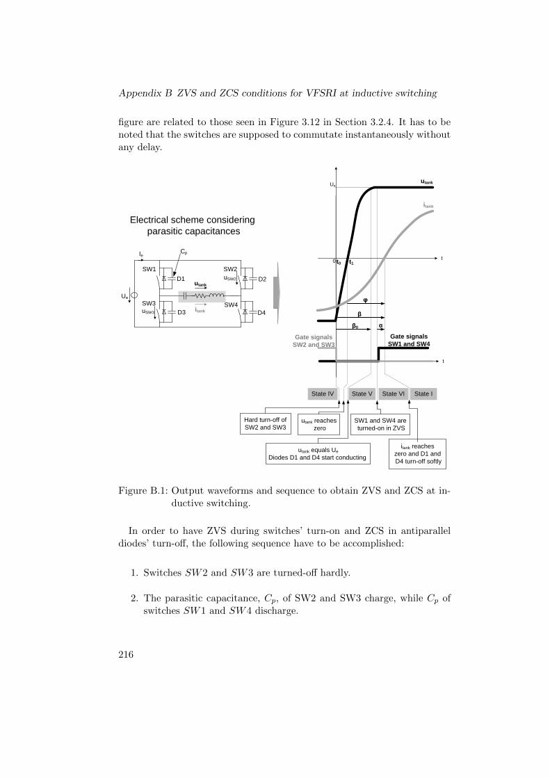
Appendix B ZVS and ZCS conditions for VFSRI at inductive switching
figure are related to those seen in Figure 3.12 in Section 3.2.4. It has to benoted that the switches are supposed to commutate instantaneously withoutany delay.
utank equals Ue
Diodes D1 and D4 start conducting
Ue
itank
utank
tIe
Ue
SW3 SW4
SW2
D3
D2
D4
utank
itank
SW1
D1
Cp
State IV State V State VI State I
itank reacheszero and D1 andD4 turn-off softly
Hard turn-off of SW2 and SW3
SW1 and SW4 areturned-on in ZVS
Electrical scheme consideringparasitic capacitances
0
t
Gate signals SW1 and SW4
Gate signals SW2 and SW3
β
β0 α
utank reacheszero
uSW3
uSW2
φ
t0 t1
Figure B.1: Output waveforms and sequence to obtain ZVS and ZCS at in-ductive switching.
In order to have ZVS during switches’ turn-on and ZCS in antiparalleldiodes’ turn-off, the following sequence have to be accomplished:
1. Switches SW2 and SW3 are turned-off hardly.
2. The parasitic capacitance, Cp, of SW2 and SW3 charge, while Cp ofswitches SW1 and SW4 discharge.
216

ii
“PhD” — 2012/5/21 — 8:58 — page 217 — #127 ii
ii
ii
B.2 Zero voltage and zero current switching conditions
3. The voltage of the charging capacitors exceeds Ue and the antiparalleldiodes D1 and D4 start conducting hardly.
4. Switches SW1 and SW4 are turned-on. The turning-on have no losses(ZVS) because their antiparallel diodes are conducting.
5. The current itanc changes polarity and conducts through SW1 andSW4, turning-off with ZCS the antiparallel diodes D1 and D4.
Considering this, the following parameters are defined (see Figure B.1):
• β is the phase-shift between the instant at which the gate signal of theswitch becomes low and itank reaches zero.
• β0 is the phase-shift between the instant at which the gate signal ofthe switch becomes low and the moment at which the voltage utankreaches Ue.
• ϕ is the phase-shift between utank and itank.
• α is the phase-shift between the instant at which the gate signal of theopposite switch becomes high and the moment at which itank crosseszero.
B.2 Zero voltage and zero current switchingconditions
In order to have the correct sequence described in the previous section forhaving ZVS and ZCS, the following condition needs to be accomplished
(β − β0) ≥ α ≥ 0 (B.1)
Considering this, two conditions for β and ϕ can be derived from thisinequality.
B.2.1 β condition
Taking the moment at which SW2 and SW3 turn-off as a zero reference,the current is expressed as
itank (t) = itanksin (ωt− β) (B.2)
217

Appendix B ZVS and ZCS conditions for VFSRI at inductive switching
Before diodes D1 and D4 starts conducting, the parasitic capacitancesCp of SW2 and SW3 have to be charged and those from SW1 and SW4discharged. Considering that the voltage across SW2 at t0 is 0 because inthe previous moments was conducting, then
uSW2 (t) =itank2ωCp
[cos (ωt− β)]t0 (B.3)
thus
uSW2 (t) =itank2ωCp
[cos (β − ωt)− cos (β)] (B.4)
The voltage utank at t0 is equal to
utank (t) = −Ue + uSW2 (t) + uSW3 (t) (B.5)
Assuming that uSW2 (t) and uSW3 (t) are equal and combining EquationB.6 with B.4, the tank voltage is
utank (t) = −Ue +itankωCp
[cos (β − ωt)− cos (β)] (B.6)
Regarding that the voltage utank is equal to Ue at β0 (Figure B.1), thefollowing equation is accomplished
utank
(β0
ω
)= Ue (B.7)
so
utank
(β0
ω
)= −Ue +
itankωCp
[cos (β − β0)− cos (β)] = Ue (B.8)
and
cos (β − β0) =2UeCpω
itank+ cos (β) (B.9)
Bearing in mind the condition expressed in Equation B.1 for having ZVSand ZCS, it can be transformed into
cos (β − β0) ≤ cos (α) (B.10)
that combined with Equation B.9 becomes
218

ii
“PhD” — 2012/5/21 — 8:58 — page 219 — #128 ii
ii
ii
B.2 Zero voltage and zero current switching conditions
2UeCpω
itank+ cos (β) ≤ cos (α) (B.11)
that leads to the following condition
β ≥ arccos[cos (α)− 2UeCpω
itank
](B.12)
Considering the limit situation where the turning-on of SW1 and SW4occur just before the crossing of zero, α = 0 and Equation B.12 becomes
β ≥ arccos[1− 2UeCpω
itank
](B.13)
B.2.2 ϕ condition
Regarding that t1 is the moment at which utank changes polarity (FigureB.1), from Equation B.6
utank (t1) = −Ue +itankωCp
[cos (β − ωt1)− cos (β)] = 0 (B.14)
Observing Figure B.1, the phase-shift between voltage and current is equalto
ϕ = β − ωt1 (B.15)
Therefore, Equation B.14 turns into
utank (t1) = −Ue +itankωCp
[cos (ϕ)− cos (β)] = 0 (B.16)
and
cos (β) = cos (ϕ)− UeCpω
itank(B.17)
Combining Equation B.13 with B.17, the following inequality emerges
cos (ϕ)− UeCpω
itank≤ 1− 2UeCpω
itank(B.18)
that simplified is equal to
ϕ ≥ arccos[1− UeCpω
itank
](B.19)
219

220

ii
“PhD” — 2012/5/21 — 8:58 — page 221 — #129 ii
ii
ii
Appendix C
Zero current and zero voltageswitching conditions for CFPRI atcapacitive switching
In Section 3.3.4, the sequence of states and events is described for an idealCFPRI commutating at zero phase-shift between voltage and current, aboveand below this frequency. Although inductive switching is presumed to avoidreverse recovery currents of series diodes, capacitive switching improves theoperation when considering the parasitic inductance Lp, as explained inSection 3.3.5. The conditions to have ZCS and ZVS considering parasiticcomponents are introduced in that section, but not completely described.
In this appendix, the conditions to have soft-switching in case of capacitiveswitching are described and developed. The explanations in this appendixare extracted from the work realized by [8, pp. 88–150], presenting just themain ideas and equations in this appendix. For facilitating the understand-ing, the explanation procedure and the notation are similar than in AppendixB.
C.1 Sequence of events considering overlap-time andparasitic components
In Section 3.3.4, Figure 3.27 shows the different states and events consider-ing an ideal inverter. In case of real converters, the overlap-time betweenswitches and the parasitic inductances have to be considered. These twoparameters affect the sequence of events and determine having ZCS duringswitches’ turn-off and ZVS during diodes’ turn-on.
The circuit incorporating the parasitic inductance of connections andswitches Lp is shown in Figure C.1. The output waveforms and the se-quence of events regarding these considerations are also presented. It has
221

Appendix C ZCS and ZVS conditions for CFPRI at capacitive switching
to be noted that in CFPRI, contrary to VFSRI, during overlap-time allswitches are conducting. In this case, switches are supposed to commutateinstantaneously without any delay. The states presented in this figure arerelated to those seen in Figure 3.27 in Section 3.3.4.
SW3 SW4
SW2
D3
D2
D4utank
itank
SW1
D1
Electrical scheme consideringparasitic inductances
itank equals Ie, changing of slope Diodes D2 and D3 turn-off
Ieitank
utank
t
State IV State V State VI State I
utank reacheszero and D2 and
D3 turn-on with ZVS
Turn-on of SW1 and SW4
SW2 and SW3 areturned-off with ZCS
0
t
Gate signals SW1 and SW4
Gate signals SW2 and SW3
β´
itank reacheszero
t0' t1'
β0' α'
φ'
LpIe
uL
iSW1
iSW3 iSW4
iSW2
Figure C.1: Output waveforms and sequence to obtain ZCS and ZVS at ca-pacitive switching.
In order to have ZCS during switches’ turn-off and ZVS in diodes’ turn-on,the following sequence have to be accomplished:
1. Switches SW1 and SW4 are turned-on. This commutation can berealized with ZVS depending on the value of Lp, whose voltage canblock the series diodes.
2. The current in the tank itank starts to decrease.
222

ii
“PhD” — 2012/5/21 — 8:58 — page 223 — #130 ii
ii
ii
C.2 Zero current and zero voltage switching conditions
3. The voltage across the parasitic inductance uL increase, opposing tothe change in current. Its value is equal to utank, annulling voltageacross switches.
4. The current in the tank itank reaches Ie, changing of slope.
5. The voltage across the inductance terminals is almost zero and diodesD2 and D3 are blocked due to voltage utank.
6. Switches SW2 and SW3 are turned-off with ZCS.
7. The voltage across the tank utanc changes polarity and diodes D2 andD3 are forward-biased with ZVS.
Considering this, the following parameters are defined (see Figure C.1):
• β′ is the phase-shift between the instant at which the gate signal ofthe switch becomes high and utank reaches zero.
• β′0 is the phase-shift between the instant at which the gate signal ofthe switch becomes high and the moment at which the current itankreaches Ie.
• ϕ′ is the phase-shift between itank and utank.
• α′ is the phase-shift between the instant at which the switches’ gatesignal becomes low and the moment at which utank crosses zero.
C.2 Zero current and zero voltage switchingconditions
In order to have the correct sequence described in the previous section andcommutate with ZCS and ZVS, the following condition needs to be accom-plished
(β′ − β′0
)≥ α′ ≥ 0 (C.1)
Considering this, two conditions for β′ and ϕ′ can be derived from thisinequality.
223

Appendix C ZCS and ZVS conditions for CFPRI at capacitive switching
C.2.1 β′ condition
Taking the moment at which SW1 and SW4 turn-on as a zero reference,the tank voltage is expressed as
utank (t) = utanksin(ωt− β′
)(C.2)
Before diodes D2 and D3 are blocked, all switches are conducting and theparasitic inductance Lp is connected to the tank. Under these circumstances,the inductance voltage is equal to the tank voltage. Thus, the current in theinductance, which is equal to itank, is as follows
iL (t) = − 1
Lp
∫utankdt =
utankωLp
cos(ωt− β′
)+ C (C.3)
Considering the current in the inductance at t′0 = 0 is −Ie (Figure C.1),Equation C.3 becomes
iL (t) =utankωLp
cos(ωt− β′
)− utank
ωLpcos(β′)− Ie (C.4)
Assuming the current at β′0 is equal to Ie, the following equation is ac-complished
itank
(β′0ω
)= Ie (C.5)
combining with Equation C.4
iL
(β′0ω
)=utankωLp
cos(β′0 − β′
)− utank
ωLpcos(β′)− Ie = Ie (C.6)
and, thus
cos(β′ − β′0
)=
2IeLpω
utank+ cos
(β′)
(C.7)
Considering the condition expressed in Equation C.1 for ZCS and ZVS atcapacitive switching and combining with Equation C.7, then
2IeLpω
utank+ cos
(β′)≤ cos
(α′)
(C.8)
that leads to the following condition
β′ ≥ arccos[cos(α′)− 2IeLpω
utank
](C.9)
224

ii
“PhD” — 2012/5/21 — 8:58 — page 225 — #131 ii
ii
ii
C.2 Zero current and zero voltage switching conditions
Taking into consideration the limit situation where switches’ turn-off oc-cur immediately before utank reaches zero, then, α′ = 0 and Equation C.9becomes
β′ ≥ arccos[1− 2IeLpω
utank
](C.10)
that represents the limit situation for having switches’ ZCS and diodes’ ZVS.
C.2.2 ϕ′ condition
Considering that t′1 is the moment at which itank changes polarity, the fol-lowing equation is obtained from Equation C.4
itank(t′1)
=utankωLp
cos(ωt′1 − β′
)− utank
ωLpcos(β′)− Ie = 0 (C.11)
Observing Figure C.1, the phase-shift between current and voltage is equalto
ϕ′ = β′ − ωt′1 (C.12)
Therefore, Equation C.11 turns into
itank(t′1)
=utankωLp
cos(ϕ′)− utank
ωLpcos(β′)− Ie = 0 (C.13)
and
cos(β′)
= cos(ϕ′)− IeLpω
utank(C.14)
Combining Equation C.10 with C.14, the following inequality emerges
cos(ϕ′)− IeLpω
utank≤ 1− 2IeLpω
utank(C.15)
that simplified equals to
ϕ′ ≥ arccos[1− IeLpω
utank
](C.16)
225

226