disclaimer - seoul national...
TRANSCRIPT

저 시-비 리- 경 지 2.0 한민
는 아래 조건 르는 경 에 한하여 게
l 저 물 복제, 포, 전송, 전시, 공연 송할 수 습니다.
다 과 같 조건 라야 합니다:
l 하는, 저 물 나 포 경 , 저 물에 적 된 허락조건 명확하게 나타내어야 합니다.
l 저 터 허가를 면 러한 조건들 적 되지 않습니다.
저 에 른 리는 내 에 하여 향 지 않습니다.
것 허락규약(Legal Code) 해하 쉽게 약한 것 니다.
Disclaimer
저 시. 하는 원저 를 시하여야 합니다.
비 리. 하는 저 물 리 목적 할 수 없습니다.
경 지. 하는 저 물 개 , 형 또는 가공할 수 없습니다.

`공학박사 학위논문
Enhanced light extraction efficiency of
OLEDs using various light extraction
structures
다양한 광추출 구조를 적용하여 향상된
유기발광다이오드의 광추출효율
2018년 2월
서울대학교 대학원
재료공학부 하이브리드재료 전공
한 경 훈

i
Abstract
Enhanced light extraction efficiency of
organic light emitting diode using
various light extraction structure
Kyung-Hoon Han
Department of Materials Science and Engineering
The Graduate School
Seoul National University
Organic light-emitting diode (OLED) is promised lighting sources as lightings
and display. In order for OLEDs to be utilized in the industry, the light extraction
efficiency of OLEDs needs to be improved further. The light extraction structure
for the display requires high light extraction efficiency improvement, low spectral
change depending on the viewing angle, low pixel blur and high contrast ratio. In
addition, fabrication process that does not damage the thin top electrode layer is
required for top-emitting OLED (TEOLED). The light extraction structure for the
lighting requires high light extraction efficiency improvement, low spectral change
depending on the viewing angle, uniform emission pattern and high color quality.
Bottom-emission OLED (BEOLED) are selected for lighting so, various light

ii
extraction method can be applied. High power efficiency and color quality are
required to compete with other light sources, including LEDs.
To enhance extraction efficiency, various light extraction methods have been
reported such as, microlens array, photonic crystal, scattering film, corrugated
device etc. Among various methods, fabrication of organic micro cone array by
vacuum deposition has potential as light extraction structure for display because of
damage-less fabrication method, high enhancement ratio and spectral stability. But,
size of the organic structure needs to be reduced in order to meet the actual display
manufacturing time. In addition, when the size of structure goes to nano, precise
optical simulation is needed for calculating optimized structure. As light extraction
structure for lighting vacuum nano hole array (VaNHA) has potential with
electrical stability due to flat surface, high extraction efficiency in comibation with
half-spherical lens. Green OLED with hexagonal VaNHA and half spherical lens
was demonstrated to extract air, substrate and waveguide mode but, for uniform
emission pattern, hexagonal pattern can’t be applied in lighting.
This thesis concerns two research topics: (1) extraction efficiency of TEOLED
with organic nano lens array (NLA) for display, and (2) extraction efficiency and
color quality of OLED with VaNHA for lightings. Our analysis shows that each
method could reach the proper light extraction method for display and lightings.
The paper consists of two parts as display and lighting. In Chapter 1,
efficiency of OLED, the optical loss path, the light extraction methods, and finite
difference time domain (FDTD) method are briefly reviewed.
In Chapter 2, we first explain the process of calculating the optical property

iii
distribution of a top-emitting OLED with light extraction structure by FDTD
method. We will discuss the computational complexity of the finite difference
method, and compare it with the calculated value of the classical electromagnetic
dipole model for the verification of the above calculation results. Next, the
calculation results of the light extraction efficiency of the TEOLED with the
hexagonal NLA are described.
In Chapter 3, we discuss the TEOLEDs with organic nano lens array (NLA).
Oragnic NLA can be fabricatied without damage to OLED, by organic vapor phase
deposition (OVPD) method. Acheivable extraction efficiency of NLA was
calculated by FDTD modelling. With simulation result, optimal distribution for
extraction is suggested and with high refractive index material and height of NLA,
higher extraction efficiency can be achieved than efficiency with organic material
(n=1.8). TEOLED with NLA showed enhanced efficiency of 50% with low pixel
blur and low spectral change with viewing angle. Blue emitting TEOLED with
NLA also showed enhancement ratio of 1.5 with low spectral change with viewing
angle.
In Chapter 4, we discuss the white OLED with randomly distributed VaNHA
with unprecedently high efficiency of EQE 78% and power efficiency of 164 lm/W.
Random pattern consists of 3 kinds of pillars with different radius of 120, 150 190
nm. With combination of half-spherical lens, almost air, substrate and waveguide
mode of light can be extracted. By mode analysis calculation, extractable light can
be increased with thick distance from metal electrode and emitting dipole. By
random distribution, white OLED with VaNHA showed uniform emission pattern

iv
and spectral stability with viewing angle. FDTD calculations were performed to
investigate the origin of high light extraction efficiency enhancement of Si3N4 and
air extraction structures. The larger the difference between the refractive index of
the dielectric layer and the nano hole array, the larger the light extraction efficiency.
In Chapter 5, we discuss the theoretically achievable color quality of white
tandem devices with various light extraction structure. First, color quality
according to the proportion of the emitting dyes was calculated which is ideal value
whole photolumeniscent (PL) spectrum is extracted. In consideration of micro
cavity, achievable color quality of device without light extraction layer, device with
half spherical lens, device with high refractive index and lens, device with high
refractive index substrate and lens and elongated distance with dipole and metal
electrode. Simulation result is compared with experiment result and matched well.
By based this model, highly efficient tandem OLED with high color temperature
( > 5,000 K) can be fabricated. The WOLEDs showed maximum EQEs of 45.6 and
79.4% and maximum LE of 48.9 and 94.0 lm/W for WOLED without and with lens,
respectively.
Keywords: Organic light emitting diodes, light extraction, finite difference
time domain, OLED display, top-emitting OLED, OLED lightings, tandem OLED,
color quality
Student Number: 2013 - 30767

v
Contents
Abstract ..................................................................................... i
Contents ....................................................................................vi
List of Tables.............................................................................ix
List of Figures............................................................................x
Chapter 1. Introduction ............................................................1
1.1. Efficiency of OLEDs............................................................................ 1
1.2. Optical loss modes in OLEDs............................................................... 3
1.3. Light extraction method of OLEDs....................................................... 5
1.4. Finite difference time domain method .................................................. 9
Chapter 2. Optical simulation method of light extraction in
top emitting organic light emitting diode using finite
difference time domain method ..............................................13
2.1. Introduction........................................................................................ 13
2.2. Methodology of optical analysis of light extraction ............................ 15
2.3 Result and Discussion ......................................................................... 21
2.4 Conclusion .......................................................................................... 30

vi
Chapter 3. Enhanced light extraction efficiency of top-
emitting OLED by using nano lens array fabricated by
organic vapor phase deposition method.................................31
3.1. Introduction........................................................................................ 31
3.2. Optical simulation .............................................................................. 34
3.3. Experiment......................................................................................... 41
3.4 Result and Discussion ......................................................................... 45
3.5 Conclusion .......................................................................................... 54
Chapter 4. Theoretically achievable light extraction efficiency
of white organic light emitting diode with vacuum nano-hole
array.........................................................................................55
4.1. Introduction........................................................................................ 55
4.2. Experiment......................................................................................... 58
4.3 Result and Discussion ......................................................................... 62
4.4 Optical simulation for extraction of waveguide mode .......................... 76
4.5 Conclusion .......................................................................................... 81

vii
Chapter 5. Theoretically achievable color quality of white
tandem OLED with various light extraction layers...............82
5.1. Introduction........................................................................................ 82
5.2 Optical simulation for high color quality ............................................. 87
5.3 Experiment.......................................................................................... 96
5.4 Result and Discussion ......................................................................... 99
5.4 Conclusion ........................................................................................ 105
Appendix................................................................................106
Bibliography ..........................................................................115
초록 ........................................................................................124
CURRICULUM VITAE........................................................129
List of Publications................................................................131
List of Presentations ..............................................................133

viii
List of Tables
Table 3.1 Summary of the simulation results of the mode fraction using the FDTD
method for different device structures. ................................................................ 36
Table 4.1 Performance of WOLEDs II w/o and w/ VaNHA and half spherical lens
at luminance of 1,000 cd m-2, except maximum PE and EQE............................... 70
Table 4.2 Performances of WOLEDs with light extraction structure reported in
literature ............................................................................................................. 73
Table 5.1 Color coordinate, CCT and CRI of WOLEDs from experiment and
simulation. ...................................................................................................... 102
Table 5.2 Performance of tandem WOLEDs without and with Half-spherical lens
(HS) of 1,000 cd/m2. ......................................................................................... 104

ix
List of Figures
Figure 1.1 Various kinds of light out-coupling losses in normal structure OLEDs.. 4
Figure 1.2 Typical external light extraction methods including (a) micro lens array
(b) luminaire, (c) substrate with scatter and (d) high refractive index. .................... 6
Figure 1.3 Typical internal light extraction methods including (a) photonics crystal
(b) corrugated device, (c) randomly dispersed nano pillar array and (d) moth eye. . 8
Figure 1.4 Classification of computational electromagnetics method................... 11
Figure 1.5 Shematic sturcture of Yee lattice in (a) FDTD simulation and (b) unit
cell...................................................................................................................... 12
Figure 2.1 (a) Simulation structure in FDTD calculation. (b) Spectrum of dipole
and time signal (inset, below). ............................................................................. 17
Figure 2.2 (a) Position of dipoles beneath the organic nanolens. Purcell factor with
each position and orientation is in inset. (b) Calculated EQE with dipoles............ 22
Figure 2.3 Calculated absorption at metal (a) and IZO (b) with dipole orientation
and position. ....................................................................................................... 24
Figure 2.4 Calculated EQEs with relative positions of horizontally (a) and
vertically (b) oriented dipoles with various radius of ONA. ................................. 26
Figure 2.5 Total EQEs and enhancement ratio of TEOLEDs with ONA at various
radius depending on the horizontally oriented dipole ratio. .................................. 27
Figure 2.6 Extraction efficiencies of TEOLED without and with ONA depending
on ETL thickness. Horizontal (a) and vertical (b) dipoles are calculated separately.
........................................................................................................................... 28

x
Figure 3.1 TEOLED with organic NLA in FDTD calculation.............................. 35
Figure 3.2 (a) Enhancement ratios of light extraction efficiency, and (b)
absorptions at Al and IZO without and with NLAs with various refractive indices
of NLA. .............................................................................................................. 38
Figure 3.3 Contour plot of enhancement ratio of light extraction efficiency with
fucntion of height and refractive index of NLA. Dotted line is plotted for
experiment value................................................................................................. 41
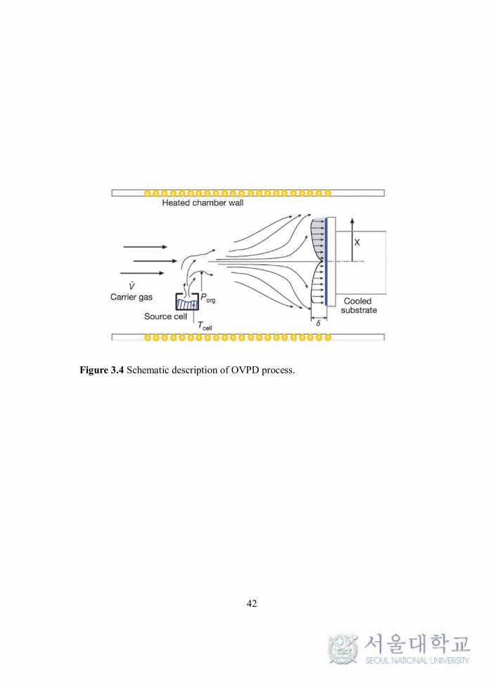
Figure 3.4 Schematic description of OVPD process. ........................................... 42
Figure 3.5 Schematic diagrams of the inverted TOLEDs before and after the NLA
integration........................................................................................................... 44
Figure 3.6 Planar (a, c) and cross sectional (b, d) SEM images of NLA 1 (a, b) and
NLA 2 (c, d), respectively, showing the creation of the nano lenses on the IZO
layer by using the OVPD process. The arrows (a, c) indicate the impingement of
the nano lenses.................................................................................................... 46
Figure 3.7 (a) The J-V-L curves, (b) the current efficiencies of the devices,
showing ~1.5 times enhancement of efficiency by the integration. ....................... 48
Figure 3.8 TEOLED without and with ONA. Less image blurring after integration.
........................................................................................................................... 49
Figure 3.9 (a) The J-V-L, (b) current and power efficiencies of blue TOLEDs
without and with NLAs. ...................................................................................... 51
Figure 3.10 Angular spectrum data of blue TOLEDs (a) without and (b) with
NLAs.................................................................................................................. 52
Figure 4.1 (a) Fabrication scheme of VaNHA substrate by robust reverse transfer

xi
process. (b) Designed pattern image of random distribution in 102 μm2 and 2D-FFT
image of the random pattern (inset). (c) Cross sectional scanning transmission
electron microscopy (STEM) image of WOLED w/ the VaNHA substrate. .......... 59
Figure 4.2 (a) Simulation structure in FDTD calculation and (b) Spectra of red,
green and blue dipole used in FDTD simulation. ................................................. 61
Figure 4.3 (a) Schematic diagram of OLED structure with energy levels. Hollow
boxes represent the LUMO (upper line) and HOMO (under line) levels of the
materials. The orange and blue shaded boxes represent the HOMO and LUMO
levels of the exciplex-forming co-hosts of the orange and blue EMLs, respectively.
The gray shaded box represents the energy level of the buffer layer (BL). The red,
green, blue, and black dashed lines show the energy levels of Ir(mphmq)2(tmd),
Ir(ppy)2(tmd), FIrpic, and B3PYMPM, respectively. The bottom line and numbers
represent the thicknesses of the layers. .............................................................. 64
Figure 4.4 (a) Simulated mode fraction as a function of the thickness of ETL (lines)
without light extraction layers and maximum external quantum efficiencies of
WOLED I and II. (b) Current density-voltage-luminous exitance characteristics of
the WOLEDs II w/ and w/o VaNHA and half-spherical lens. Inset: Relative EL
spectra of device w/o and w/ VaNHA and lens at 3 mA/cm2 in an integrating sphere.
(c) EQEs of the WOLEDs with/without VaNHA and half-spherical lens as a
function of luminous exitance. (d) Luminous efficacies of WOLEDs w/o and w/
VaNHA and half-spherical lens as a function of luminous exitance. ..................... 66
Figure 4.5 Contour plots of extraction efficiency as functions of ETL
(B3PYMPM) and HTL (TAPC) thicknesses. (a) Air mode and (b) extractable mode

xii
(sum of air, substrate and waveguide mode). The recombination zone was assumed
to be located in the middle of the orange and blue emission layers. Device structure
was the same as Figure 4.2 with varying thicknesses of TAPC and doped
B3PYMPM layers. The exciton density ratios of the blue, green, and red emitters
were assumed to be 0.14, 0.26 and 0.60............................................................... 67
Figure 4.6 (a) Current density-voltage-luminous exitance characteristics of the
WOLEDs I w/ and w/o VaNHA and lens. (b) Relative EL intensities of the device
w/o and w/ VaNHA and lens at 3 mA/cm2 measured in an integrating sphere. (c)
EQEs of the WOLEDs with/without VaNHA and lens as a function of luminous
exitance. (d) Luminous efficacies of WOLEDs w/o and w/ VaNHA and lens as a
function of luminous exitance. ............................................................................ 68
Figure 4.7 Comparison of the efficiencies of WOLEDs demonstrated in this work
with the state-of-the-art WOLEDs.31,21,77-80,34,81-83................................................. 72
Figure 4.8 (a) Normalized electroluminescence (EL) spectra of WOLED I and II
without and with VaNHA measured in the normal direction to the glass substrates
at 1,000 cd m-2. The CCT and CRI are given for each spectrum. (b) Angle
dependent EL spectra of WOLED II with VaNHA. Inset: Photographs of the
WOLEDs with (left) and without VaNHA (right). ............................................... 74
Figure 4.9 (a) Electric field of WOLEDs with bare glass substrate. (b-g) Electic
field of WOLEDs with a VaNHA substrate having different refractive index of
dielectric material, ndielectic material=1.3, 1.7, 1.9, 2.1 and 2.3, respectively. .............. 79
Figure 4.10 (a) Contour plot of enhancement ratio with various refractive index of
dielectric layer and nanohole array. White dotted line is area where refractive index

xiii
of dielectric and nanohole is same. Calculated enhancement ratios (b) with
refractive index of dielectric layer (refractive index of hole is fixed as 1.0.) and (c)
with refractive index of hole array (refractive index of dielectric layer is fixed as
2.0). .................................................................................................................... 80
Figure 5.1 Parameters of color quality in lightings. ............................................. 84
Figure 5.2 (a) Reported CIE color coordinate of state-of-the-art WOLEDs and (b)
table of corresponding CRIs, CCTs and PEs........................................................ 85
Figure 5.3 (a) Molecular structure, PLQY, horizontally oriented dipole ratio of
phosphorescent dyes (b) spectra and (c) CIE cordintaes of corresponding
phosphorescent dyes. .......................................................................................... 88
Figure 5.4 (a) Contour plot of acheivable CIE coordinate and CRI with
combination of Ir(mphmq)2tmd, Ir(3’,5’,4-mppy)2tmd and FIrpic. (b) Contour plot
of acheivable CIE coordinate and CRI with combination of Ir(mphmq)2tmd,
Ir(3’,5’,4-mppy)2tmd and FCNIrpic..................................................................... 90
Figure 5.5 Calculated spectrum of red, green, blue dyes in WOLEDs with various
light extraction structure...................................................................................... 91
Figure 5.6 Schematic descriptions of (a) OLED without light extraction structure,
(b) OLED with half-spherical lens, (c) OLED with high refractive index substrate
and lens and (d) OLED with high refractive index substrate and lens with elongated
electron transport layer. ....................................................................................... 93
Figure 5.7 Contour plot of CIE coordinate and coresponding CRI of (a) WOLEDs
without light extraction layer, (b) WOLEDs with half-spherical lens and (c)
WOLED with high refractive index substrate and lens with elongated ETL. ........ 94

xiv
Figure 5.8 Devices structure of tandem white OLED. ....................................... 97
Figure 5.9 (a) EL spectrum of WOLEDs without and with lens and calculated
spectrum of corresponding devices (b) Color coordinates of WOLEDs from
experiment and calculation................................................................................ 101
Figure 5.10 (a) J-V-L of WOLEDs without and with half spherical lens and (b)
EQEs and Power efiiciencies with function of luminance of WOLEDs without and
with half spherical lens...................................................................................... 103

1
Chapter 1. Introduction
1.1 Efficiency of Organic light emitting diodes
There are many ways to show the efficiency of OLEDs such as external
quantum efficiency (EQE), power efficiency (PE, lm/W), current efficiency (CE,
Cd/A) lumen per dollars etc. Among those values, EQE is one of the widely used
assessment matrics in efficiency of light-emitting diodes. The EQE, EQEh , is
defined as the number of photons per injected electron;1i.e.,
i n t / ( , ) ( , )E Q E o u t S T ef f P L o u tqh h h g h f h= ´ = ´ ´ G ´ Q G (1)
Where,IQEh is internal quatum efficiency (IQE),
outh is out-coupling
efficiency, g is the charge balance factor, /S Th is the fraction of radiative
excitons (/S Th =0.25 for fluorescent emitters and
/S Th =1 for phosphorescent
emitters), effq is the effective radiative quantum yield of the emitter in the cavity
structure,PLf is photoluminescent quantum yield of emitting material, G is a factor
related to device structure, Q is farction of horizontally oriented dipoles
respectively.
The IQE of OLEDs can reach 100% by exploiting various materials such as
organic materials harvesting triplet excitons in the emission process,2,3 p- or n-type
dopants in the transport layers,4,5 or charge injection layer6 to improve the charge
injection. However, outh of OLEDs is limited in 20~30% (in consideration of
isotropic orientation) due to waveguide and total internal refraction (TIR) which

2
come from the large difference in the refractive index between the organic layer
and air. Therefore, out-coupling efficiency remains the biggest hurdle to improve
the efficiency of OLEDs.

3
1.2 Optical loss modes in OLEDs
As shown in Figure 1.1, the optical modes are composed of the air mode, the
substrate mode, the waveguide mode, the surface plasmon polaritons (SPPs), and
the electrode absorption.7-11 The OLEDs consist of an organic layer (n = 1.7~1.8)
sandwiched between a transparent conducting oxide (TCO), such as indium tin
oxide or indium zinc oxide (n = 1.9~2.1) on a glass substrate (n = 1.45~1.55), and a
reflective metal electrode. Due to large refractive index difference between air and
organic, significant amount of light is waveguided in the ITO-organic stack
(waveguide mode). And total internal reflection occurs between the glass and the
air interface, and light is transmitted back to the organic stack without being
extracted. Due to the SPPs at the interface of the metal and the organic, generated
light is dissipated in absorptive cathode region. A small portion of light also is
absorbed at the TCO. Thus, light extraction efficiency of the OLEDs which has
emitting dopoles with isotropic orientation and without light extraction layer is
limited in only 20~30%.

4
Figure 1.1 Various kinds of light out-coupling losses in normal structure OLEDs.

5
1.3 Light extraction methods of OLEDs
There has been tremendous light extraction methods reported. Among various
classifications, position of light extraction structure is good parameter to determine.
Generally, external method means light extraction structure is positioned outside
substrate and internal method means light extraction layer is positioned between
substrate and OLED stack.
Figure 1.2 shows typical external light extraction methods including micro
lens array (MLA),12-14 luminaire,15 substrate with scatter,16-20 high refractive
index21-22 and roughned surfaces.23-24 MLA, luminaire and roughened surfaces
extracts light by reducing incident angle below critical angle between air and
structure. Scatter causes multiple scattering and ultimately converts the light above
the critical angle into an angle within the critical angle. The external light
extracting structure has advantages that it is easy to fabricate and apply, but the
extractable light is limited to the substrate mode. In display, external light
extraction structure generates a blurring effect on the display panel because of the
presence of thick substrate.
Figure 1.3 shows typical internal light extraction methods including photonic
crystal (PC),25-28 randomly dispersed nano pillar array,29,30 low refractive index
grid,31,32 moth eye,33,34 nanoparticle35 and corrugated device etc.36-39 Nano pillar
array extracts waveguide mode by giving additional momentum. Generally,
periodic array (PC) extracts specific wavelength and distort the angular spectrum.
For extracting broadband of light randomly dispersed pillar array is used for light

6
Figure 1.2 Typical external light extraction methods including (a) micro lens array
(b) luminaire, (c) substrate with scatter and (d) high refractive index.

7
extraction. Moth eye structure extracts the light by anti-reflection effect which
comes from impedance matching by graded index. The internal light extraction
structure has the advantage of a potentially high extractable light, but only methods
that do not adversely affect the reliability of the OLED can be used. The corrugated
device extracts the SPP mode resulting to high light extraction efficiency, but non-
uniform electric field is formed between the electrodes to change the electrical
characteristics of the device.
Besides, device tuning without structure can be included as light extraction
method. Those parameters are micro cavity effect,40,41 orientation of emitting
dipole,42,43 low refractive index of organic material44 and selection of alternative
electrode45,46 etc.

8
Figure 1.3 Typical internal light extraction methods including (a) photonics crystal
(b) corrugated device, (c) randomly dispersed nano pillar array and (d) moth eye.

9
1.4 Finite difference time domain method
To reduce the burden of repetitive experiments, simulation of the proposed
optical structure before the fabrication is important. Figure 1.4 shows classification
of computational electromagnetics. High frequency method is used for calculation
of OLED with micro structure with combination of electrical dipole model.14,20
Light extraction efficiency of OLED with nano structure is solved only low
frequency method. In computational electromagnetics, a method is rigorous if there
exists resolution parameter that when taken to infinity, finds an exact solution to
Maxwell’s equations. Finite difference time domain (FDTD) method have
advatages when compared to finite elemet method (FEM) such as no pre- of post-
processing (required FEM), inclusion of nonlinearity much easier (than FEM),
time-marched arrays of fields for intuitive movie generation and easy to get
frequency response (FFT) etc.
The FDTD method is a numerical analysis technique used for solving
Maxwell's equations in complex geometries. The time-dependent Maxwell's
equations (in partial differential form) are discretized using central-difference
approximations for the spatial and temporal partial derivatives. Since it is a time-
domain method, FDTD simulations can cover a wide frequency range (by
exploiting Fourier transform properties) with a single simulation run and handle
nonlinear material properties in a natural way. In FDTD, space is discretized into
box-shaped cells, which are small in comparison to the wavelength (Figure 1.5).
The so-called cubic Yee cell uses the following conventions: the electric field is

10
defined at the edge centers of the cube;47 the magnetic field is defined at the face
centers of the cube; the electric permittivity/conductivity is defined at the cube
center and the magnetic permeability/magnetic loss is defined at the cube corners.
From the Noda et al.’s calculation of mode fraction of OLED,48 FDTD method
have been utilized as optical analysis tool for FDTD method for far-field
distribution,49-50 light extraction efficiency51-53 and transmittance of nanostructure.54

11
Figure 1.4 Classification of computational electromagnetics method.

12
Figure 1.5 Shematic sturcture of Yee lattice in (a) FDTD simulation and (b) unit
cell.

13
Chapter 2. Optical simulation method of light extraction in
top emitting organic light emitting diode using finite
difference time domain method
2.1 Introduction
Organic light emitting diodes are promised as next generation display sources
for high color quality, fast response time, applicability to flexible substrate and
potentially low cost. In order to commercialize OLEDs successfully, power
efficiency of OLEDs needs to be improved further. Most of efficiency loss is due to
low light extraction efficiency from high refractive index of emitting material.
Although there have been tremendous researches for increasing light extraction
efficiency,12-39 consideration on how to apply the light extraction layer in
fabrication process is insufficient. In display, top emitting OLEDs are utilized for
high aperture ratio and fabrication sequence of transistor and display. For inhibiting
damage to OLED stacks, only damage-less method can be selected as fabrication
method of light extraction layer. Nowadays, several reports such as vacuum
evaporatio,55,56 and reflective subelectrode grid57 have shown potential for
applicability in industrial level. Especially fabrication of organic nanolens array
have advantages in damage-less method, manufacturing process that does not break
vacuum, large area process and low fabrication cost. As the feasibility of the light
extraction structure on top-emitting device increases, the demand for an accurate

14
calculation of light extraction efficiency also increases.
In this report, we propose calculation method of Purcell factor which
correlates totally generated power of electric dipole and light extraction efficiency
of top-emitting OLED with organic nanolens array using finite difference time
domain (FDTD) method. FDTD method have been utilized as calculation tool for
mode fraction,48 far-field distribution,49,50 light extraction efficiency51-53 and
transmittance of nanostructure.54 Calculation of TEOLEDs with nanostructure has
not been reported well because of difficulty in calculation of Purcell factor. Purcell
factor is affected by reflected light to emitting dipole and reflected light is
complicated when the nanostructure is near dipole.58,59 For precise calculation,
position and size of the power monitors should be carefully set and the Purcell
factors calculated at each position should be averaged. Commercial-grade
simulator (FDTD solutions) was used to perform whole calculation.60
We investigate the calculation factors affecting in Purcell factor. By using
optimized mesh size, Purcell factor and light extraction efficiency is calculated. For
verify the modelling, light extraction efficiency and Purcell factor of TEOLED
with IZO and Al are compared with results using classical electric dipole model.61-
63 TEOLEDs with organic nanolens array with hexagonal distribution and radius of
200, 300 and 400 nm and fill factor of 0.7 are utilized. From position dependent
calculation, exact light extraction efficiency is calculated. Moreover, we also
calculated energy loss in metal electrode and anode. We also calculated extraction
efficiencies with distance from dipole to metal electrode and horizontal dipole ratio.

15

16
2.2 Methodology of optical analysis of ligh extraction
2.2.1 Simulation structure
Simulation structure is in Figure 2.1 (a). Top emitting OLEDs with IZO as top
electrode is designed for calculation. TEOLED consists of Al (100 nm, n= 0.6,
k=0.1), organic (160 nm, n=1.8) and IZO (60 nm, n=2.02, k=0.068). Refractive
indices of organic materials are similar each other and set as 1.8. Organic layers
consist of hole transporting layer (HTL, 70 nm), emitting layer (EML, 30 nm) and
electron transfer layer (ETL, 20, 40, 60 and 80 nm). In order to observe the
tendency according to the micro-cavities, optical calculations were carried out with
different ETL thicknesses. Fill factor of organic nanolens array is 0.7 and radius are
varied from 200 nm to 400 nm.
Simulation structure is 8000 * 8000 * 780 nm3 and calculation time is 500 fs.
Perfect matched layer (PML) is used as boundary condition of simulation. Other
boundary method such as metal, Bloch induces artificial electric fields to dipole
and results in inaccurate Purcell factor. Conductivity of PML is selected with sigma
of 10 and kappa of 0.5 to avoid divergence of calculation.
The spectra used in this calculation and the signals in time domains are shown
in Figure 2.1 (b). To realize green color, we set up a dipole with a wavelength of
510 nm and set the pulselength to 45 fs so that the wave packet is set close to the
continuous monochromatic wave. Z direction PML was set at a distance of one

17
Figure 2.1 (a) Simulation structure in FDTD calculation. (b) Spectrum of dipole
and time signal (inset, below).

18
wavelength from the IZO to prevent coupling with the evanescent field
formed in the IZO-air. The power monitor is set between the PML and the IZO (or
organic lens), the distance corresponding to the half wavelength.
2.2.2 Mesh size
Mesh size in finite difference method is one of the most important parameters
in finite difference method (FDM). To figure out dependency of mesh size on
calculation accuracy, various size of mesh is utilized. The OLED used in this
calculation does not have a light extraction structure. Since the horizontal direction
is symmetrical in OLED without extraction layer, mesh length in the x and y
directions is set to the same size. It can be seen that the horizontal mesh length
does not significantly affect the calculation results, but the calculation results vary
greatly depending on the mesh length in the vertical direction only. The calculated
value decreases gradually from 10 nm and converges from 3 nm. In this report,
mesh size with 10 * 10 * 3 nm3 is used for calculation time. Trade-off between
accuracy and simulation time in FDM is general.
Purcell factor is changed inside cavity or resonator. In FDTD model,
calculation of Purcell factor is one of the most important parameters because total
emitted light in calculation is same with Purcell factor. For calculation of Purcell
factor, power monitors surrounds the emitting dipole with distance. Distance of
power monitors
needs to be carefully selected. When monitor is near the dipole, inaccuracy is
increased. In otherwise total generated power is decreased due to absorption at
metal and IZO and this absorption is not unwanted result in Purcell factor. Distance

19
from 3 meshes is optimized distance for calculating Purcell factor.
3.2.3 Comparison with CPS model
With these parameters, light extraction and Purcell factor of TEOLED with Al
and IZO as top electrode are calculated. For verifying the model, classical electric
dipole model was utilized and compare the both results. Figure 2.3 shows the
extraction efficiency and Purcell factor of both device and simulation structure is in
inset of Figure 2.3. Simulation results from FDTD method is matched well with
result from CPS model. Dependency with orientation of dipole and thickness of
ETL is also matched in FDTD simulation. This result proves the accuracy of FDTD
modelling for precise calculation of Purcell factor and extraction efficiency.

20
Figure 2.2 Calculated Air mode and Purcell factor of TEOLEDs with various ETL
thickness. IZO of 60 nm (a) and Al of 20 nm (b) are used as top electrode of
TEOLEDs. Both result is compared with results from CPS model (line).

21
2.3 Result and Discussion
The Purcell factor and the light extraction efficiency of the top OLED with the
structure shown in Figure 2.1 (a) were calculated. The radius of the lens used is 300
nm and the fill factor is 0.7. Positions of dipoles are shown in Figure 2.3 (a).
Positions are varied with 0, 0.25, 0.5, 0.75 and 1 radiuses, center of 2 lenses with x
direction. Calculated Purcell factors corresponding to each position were collected
together with the inset of Figure 2.3 (a). Purcell factors changed with dipole
position. The Purcell factors of TEOLED with ONA varied greatly depending on
the location. This large fluctuation shows that calculation of the device whose light
extracting structure is close to the light emitting layer is difficult.
The extraction efficiency according to the position and orientation of the
dipole is shown in Figure 2.3 (b). The light extraction efficiency is the highest at
the center of the lens and gradually decreases as the distance from the center of the
lens increases. Some parts are less efficient than devices without light extraction
structures. In the device with the light extraction structure, the light extraction
efficiencies of the dipoles in the x and y directions are different, and the difference
in the end portion and the outer portion of the nano-lens increases. Vertically
oriented dipoles have much lower absolute values but, enhancement ratio is high
due to low light extraction efficiency of device without ONA.
For understanding the other property, absorption at metal and IZO is
calculated in Figure 2.4. In the time domain calculation, we cannot obtain a result

22
Figure 2.3 (a) Position of dipoles beneath the organic nanolens. Purcell factor with
each position and orientation is in inset. (b) Calculated EQE with dipoles.

23
corresponding to the correct mode fraction, but we can calculate the total
absorption value by setting the position of the power monitor around the material
having extinction coefficient. The total amount of energy dissipated in the metal
was calculated by setting the power monitor at the interface between the organic
material and the metal. The energy difference between the transmitted
electromagnetic wave and the reflected electromagnetic wave on the power
monitor is defined as the absorbed energy by the metal. Naturally, the absorbed
value had the opposite tendency to the extracted light. In vertically oriented dipoles,
more than 85% of light is absorbed by the metal. Since the vertically oriented
dipole has high SPP portion, the organic nano-lens array formed on the IZO does
not affect the extraction.
The following equation was used to calculate the total amount of energy
absorbed in IZO.64
����(�⃗, ��) = � × Im[����] × |����(�⃗, ��)|� (2)
To calculate the energy absorbed by the IZO, a 3-d power monitor of the same
size as the entire IZO region was set. The amount of absorption in the horizontally
oriented dipole was more than that in the vertically oriented dipole.
The light extraction efficiencies were calculated when the fill factor of the
nanolens array was fixed at 0.7 and radius of lens was varied with 100, 200, 300,
400 and 500 nm. Interestingly, the tendency of extraction efficiency according to
dipole location varied significantly with the radius of nanolens. The larger the
radius of the nano-lens array, the higher the extraction efficiency at the center of

24
Figure 2.4 Calculated absorption at metal (a) and IZO (b) with dipole orientation
and position.

25
the lens, but the more the extraction efficiency decreases as the distance from
the center of the lens increases. When the radius is 300 nm, the difference
according to the direction of the horizontal orientation dipole is largest. Since the
space of organic lens is a sub-wavelength region, it is not significantly influenced
by the direction of the dipole in radius 100 and 200 nm. Light extraction efficiency
of TEOLED with radius of 100 nm is lower than that of the device without ONA.
In the vertically oriented dipoles, the radii of the nanolens did not make a large
difference.
Enhancement ratio of horizontally oriented dipole ratio is calculated in Figure
2.5. Enhancement ratio is increased with vertical dipole but, overall extraction
efficiency is high with full horizontal layer. The light extraction efficiency of the
device using the 400 nm radius is the highest. Since the calculation results are
obtained when the fill factor is fixed, this calculation value cannot be regarded as
the maximum improvement of the light extraction method using ONA. This result
shows that the size of the nanostructure greatly affects the light extraction
efficiency and the size control is important in the application of the upper light
emitting OLED.
The structure of the nanolens was fixed at a radius of 200 nm and a fill factor
of 0.7, and the light extraction efficiencies are calculated by changing the thickness
of the ETL (Figure 2.6). For comparison, the mode fraction of a device without a
light extraction structure was calculated using the CPS model. Device without and
with

26
Figure 2.5 Calculated EQEs with relative positions of horizontally (a) and
vertically (b) oriented dipoles with various radius of ONA.

27
Figure 2.6 Total EQEs and enhancement ratio of TEOLEDs with ONA at various
radius depending on the horizontally oriented dipole ratio.

28
Figure 2.7 Extraction efficiencies of TEOLED without and with ONA depending
on ETL thickness. Horizontal (a) and vertical (b) dipoles are calculated separately.

29
ONA have the highest extraction efficiency at ETL of 40 nm. The
enhancement ratio of extraction efficiency of devices using thin ETL (30 nm) is
higher. If the ETL is too thick, the ratio of the light traveling in the horizontal
direction of the device increases, which is not very advantageous for light
extraction. The light extraction efficiency of the vertical dipole of the device with
ETL thickness of 60, 80 nm is similar to that before light extraction.

30
2.4 Conclusion
Simulation parameter is carefully selected for calculation of extraction
efficiency and Purcell factor. With those parameters, result from FDTD model is
matched well with result using CPS model. Dipole position is critical parameters in
TEOLED with light extraction structure. Purcell factor is also changed much with
dipole positions. Light extraction efficiency is high at center of nanolens and
decreased with distance from center of dipole. Total enhancement ratio is only 20%
which is calculated with radius of 400 nm. Absorption at bottom metal electrode
and IZO layer is calculated and tendency of both are matched with tendency of
extraction efficiency. From this modelling, TEOLED with extraction layer of
nanosize can be calculated.

31
Chapter 3. Enhanced light extraction efficiency of top-
emitting organic light emitting diode by using nano lens
array fabricated by organic vapor phase deposition method
3.1 Introduction
A lens array containing multiple lenses with a lens diameter of <1 mm has
been used as an optical functional film (a layer having functions of light extraction,
refraction or scattering et al.) working in lights in a particular range of wavelength.
The lenses have curved surface such as a hemisphere to act on the light. Size
control is an essential technology because any kind of light can be selected by
controlling the diameter. To fabricate the lens array, other technology such as a
mask, a surface treatment and a molding has been combined with a deposition
process,55,56 because all deposition apparatuses have been designed to manufacture
films with even surface. This results in the complicated and difficult fabrication of
the lens array. A light extraction layer of organic light emitting diodes (OLEDs) can
be one of the great applications of the lens array, since OLEDs have become
dominant in small sized displays and are increasingly used in the production of
large sized TVs and solid stated lightings. Improving efficiency has always been an
important issue in OLEDs to reduce power consumption in all of these applications.

32
Light extraction is one of the most important technologies for improving the
efficiency of OLEDs, because 60~80% of the generated light is trapped in the
OLEDs as the substrate confined mode, the waveguided mode and the surface
plasmon polariton mode, if there are no extraction films. Large number of methods
integrating either an internal or external light extraction layer or combining both
have been developed to enhance the light extraction efficiency to demonstrate high
external quantum efficiency.12-39 Despite such development, light extraction
technologies are still not used for display applications because of the image
blurring issues for bottom emission OLEDs used for TVs coming from thick
substrate on the one hand, and difficulties of integration of the extraction methods
to the completed OLEDs in top-emitting OLEDs (TOLEDs) used for small size
displays on the other hand. The image blurring issue must also be considered in
TOLEDs even though it is less serious, because thin layers (an encapsulation layer
and a micro lens array) in the order of a few micrometers are applied on the top
electrode in the TOLEDs used for small sized displays.65 Most of the light
extraction layers fabricated by wet processing are not compatible with the current
TOLED manufacturing process. Furthermore, the pixel size of active matrix OLED
(AMOLED) displays for mobile devices is continuously decreasing following the
increase in an image resolution. Thus, the NLA with sufficiently smaller size (<1
um) is necessary to avoid the image quality degradation. The development of a
deposition process for creating the NLA without combining the additional
technique and compatible with the current OLED fabrication technologies is one of
the greatest advances in low cost, short tact time and high resolution display

33
applications. In this work, we report an organic NLA fabricated using an organic
vapor phase deposition (OVPD) without combining that. Formation mechanism of
the NLA is investigated by using a grazing-incidence small-angle Xray scattering
(GI-SAXS) analysis. To elucidate the efficacy of the NLA, optical simulations are
performed. OLEDs without and with the NLAs are fabricated and characterized.

34
3.2 Optical simulation
The Lumerical finite difference time domain (FDTD) solutions package was
utilized as the simulation program.60 The size of the computational domain and the
unit mesh was 10 × 10 × 0.67 μm3 and 10 × 10 × 2 nm3, respectively (Figure 3.1).
A perfectly matched layer (PML) was used as the boundary condition. A single
electric dipole was utilized as the light source which had a peak of 510 nm and a
full width at half maximum of 38 nm, and was positioned at the center of the
simulation structure. The calculations were carried out until 0.1% of the total
power was left in the calculation domain.
The simulation results are summarized in Table 3.1. Use of NLA 1 and NLA 2
increased the light output efficiency by a factor of 1.02 and 1.48, respectively. The
∼1.5-fold change in the NLA 2 based device is believed to be due to the reduction
of the guided modes by scattering at the NLA pattern, which also leads to a
decrease in the absorption loss at the interface between the metal and organic layers.
However, the light output ratio in the NLA 1 simulation is scarcely changed, which
is believed to be due to the small size of the NLA which does not scatter the light
efficiently.
Without the NLA, a strong evanescent field is present at the IZO-Air interface
due to the large difference in refractive indices between IZO (2.05) and air (1.0).
The electric field intensity abruptly decreases from the IZO-Air interface to the air

35
Figure 3.1 TEOLED with organic NLA in FDTD calculation.

36
Table 3.1 Summary of the simulation results of the mode fraction using the FDTD
method for different device structures.
Structure Extracted Wave-guided Absorption by metal
fraction Enhancement ratio
fraction fraction
w/o 0.304 - 0.271 0.425
w/ NLA1 0.311 1.02 0.261 0.428
w/ NLA2 0.451 1.48 0.183 0.366

37
region. However, with the NLA, the electric field intensity is significantly
reduced in the whole device, most greatly reduced at the IZO-NLA interface (ie,
IZO-Air interface without NLA), and shows much slower decrease from the IZO-
NLA interface to the NLA region. This indicates that the NLA extracts light
otherwise trapped in the device66,67 by mainly reducing the waveguide loss. Higher
refractive index of the NLA provides lower electric field intensity at the IZO-NLA
interface. This suggests that the light extraction efficiency can be further increased
by using a higher refractive index material for NLA, corresponding to the results
shown in Figure 3.2 (a). NPB with a refractive index of 1.8 is used for the NLA in
the device fabrication, hence it is predicted that the efficiency is increased
approximately 1.52 times by NLA integration in the experiments.
The total amount of energy absorbed in the Al and the IZO electrodes is
calculated.64 The absorption loss is decreased by introducing the NLA and by
increasing its refractive index (Figure 3.2 (b)). The integration of the NLA with a
refractive index of 1.8 (NPB) provides the larger decrease ratio of absorption at the
IZO compared to that at the Al (0.13 vs 0.09).
Interestingly, even though the differences in refractive indices between NLA
(1.8-2.1) and air are similar to that between IZO (2.05) and air, the electric field
intensities at the NLA-Air interface are half of that at the IZO-Air interface. In
addition, the electric field curves at the NLA-Air interface are very smooth.
Moreover, there is a significantly slower intensity decrease from the NLA-Air
interface to the air region (with NLA), compared from the IZO-Air interface to the
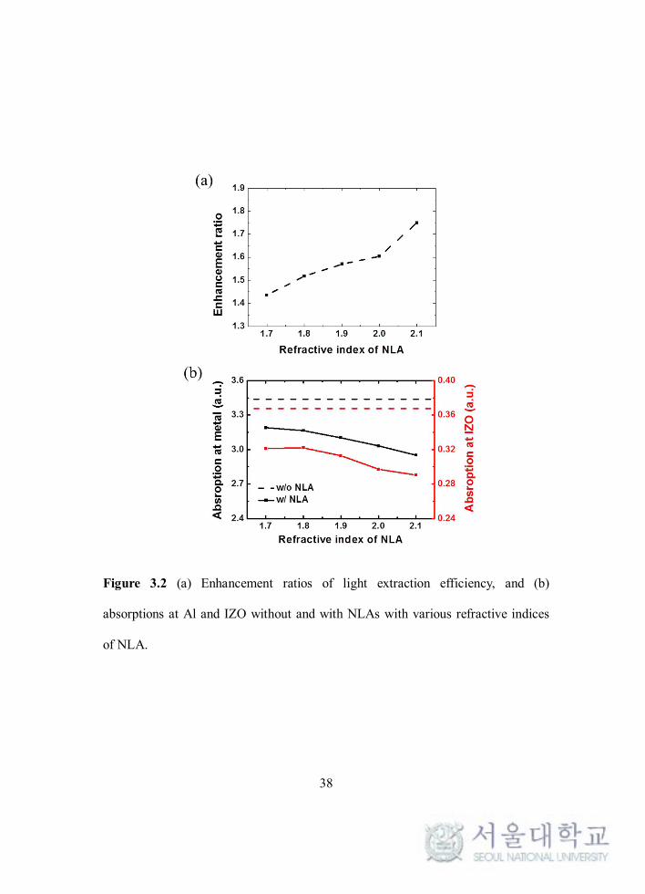
38
Figure 3.2 (a) Enhancement ratios of light extraction efficiency, and (b)
absorptions at Al and IZO without and with NLAs with various refractive indices
of NLA.

39
Figure 3.3 Contour plot of enhancement ratio of light extraction efficiency with
fucntion of height and refractive index of NLA. Dotted line is plotted for
experiment value.

40
air (without NLA). Therefore, we believe that the NLA efficiently sends the
light out to the air, as an optically excellent scattering structure.
It has been reported that scattering layers based on 240 nm size nanoparticles
fabricated by using solution processes enhance the efficiency and improve the color
stability of bottom-emitting white OLEDs.67,68 The nanoparticle process is not
compatible with the processes in the current OLED industry, because it uses a wet
method. The nanoparticles are internal scattering layers, as they are located
between the substrate and the bottom electrode. NLA in this study is an external
scattering layer because it is formed on the top electrode. To experimentally
demonstrate the effectiveness of the NLA on the blue OLEDs, devices are
fabricated and measured.
41
3.3 Experiment
3.3.1 Fabrication of NLA
The NLA was fabricated on indium zinc oxide (IZO) film using the OVPD.
Neither a lithography, a shadow mask, a surface treatment, nor a molding was
combined with the OVPD process. N,N’-Di(1-naphthyl)-N,N’-diphenyl-(1,1’-
biphenyl)-4,4’-diamine (NPB, purity >99.9 %) powders were put into a vaporizer
and then heated to generate organic vapors. The vapors were transferred by means
of a nitrogen gas and deposited on the specimens (Figure 3.4). Prior to the
deposition, the samples were transferred to main chamber with a base pressure of
<10-2 Torr, via a load-lock chamber. The nitrogen gas flow rate was 100 sccm. The
NLA was grown at a growth rate of ~25 nm/min. The substrate temperature was -
10°C.
3.3.2 Fabrication and evaluaition of green TEOLED
The inverted TOLED devices were fabricated on glass-substrates pre-
patterned with a 70 nm thick indium tin oxide. The cathode and the organic layers
were deposited using thermal evaporation processes at a pressure of 3x10⁻⁷ Torr.
The device structure was: aluminium (Al, 70 nm) / 7wt% Rb2CO3 doped
B3PYMPM (40 nm) / B3PYMPM:TCTA:Ir(ppy)2acac (0.46:0.46:0.08 wt%, 30 nm)
42
Figure 3.4 Schematic description of OVPD process.

43
/ TCTA (10 nm) / TAPC (10 nm) / 10wt% ReO3 doped TAPC (40 nm) /HATCN (40
nm), where B3PYMPM, TCTA, Ir(ppy)2acac, TAPC, and HATCN represent bis-
4,6-(3,5-di-3pyridylphenyl)-2-methylpyrimidine, 4,4',4''-tris(carbazol-9-yl)tripheny
lamine, bis(2-phenylpyridyl) iridium(iii) acetylacetonate, 1,1-bis-(4-bis(4-methyl-
phenyl)-aminophenyl)-cyclohexane, and 1,4,5,8,9,11-hexaazatriphenylene hexacar
bonitrile, respectively. The IZO was sputter deposited on the HATCN film by using
facing targets at room temperature. The NLA was fabricated on the IZO by using
the OVPD (Figure 3.5). The J-VL characteristics were measured using a Keithley
2400 programmable source meter. The angular distribution of the
electroluminescence intensity was measured using the Keithley 2400
programmable source meter, a rotation stage and an Ocean Optics S2000 fiber
optic spectrometer.
3.3.3 Fabrication and evaluaition of blue TEOLED
Blue fluorescent OLEDs with an inverted top emitting structure were
fabricated on glass/indium tin oxide (ITO, 70 nm) substrates. Following the
aluminium (Al, 70 nm) cathode deposition, organic layers composed of 1 wt%
Rb2CO3 doped B3PYMPM (40 nm) / B3PYMPM (10 nm) / B3PYMPM:mCP:10
wt% TBPe (30 nm) / mCP (10 nm) / 10 wt% ReO3 doped mCP (10 nm) / HATCN
(50 nm) were formed using thermal evaporation processes without breaking the
vacuum, where mCP is abbreviated forms of N,N’-dicarbazolyl-3,5-benzene.

44
Figure 3.5 Schematic diagrams of the inverted TOLEDs before and after the NLA
integration.

45
3.4 Result and discussion
To fabricate the NLA, the OVPD was introduced, because it enables an
accurate control over the transport rates of the precursors by separately controlling
carrier gas flows and the temperature of each source.69-71 NPB was chosen as the
lens material, since it has a refractive index close to that of IZO, the transparent top
electrode used for this study. The OVPD is a dry process so that it is fully
compatible with current fabrication processes of OLEDs.
Scanning electron microscope (SEM) images of the NLAs fabricated on the
IZO layers using the OVPD are shown in Figure 3.6. When thermal evaporation
process was used to fabricate the NPB film, we did not get the NLA but a planar
thin film. Figs. 1a and 1b show that hemispherical nano lenses with a diameter of
~80 nm (NLA pattern 1) were formed, and some of them were impinged as
indicated by arrows.
By controlling the fabrication process including the vaporizer pressure, nano
lenses with a diameter of 200-700 nm (NLA pattern 2) could be fabricated as
presented in Figure 3.1 (c) and 3.1 (d), indicating that the diameter is controllable
by controlling process parameters. The coverage ratio of nano lens to total surface
is ~70%. These morphologies indicate that islands nucleate at isolated areas and
grow larger to impinge with other islands.72
The NLA 2 with a larger lens size has a greater tendency of the coalescence of
the nano lenses, compared to the NLA 1 with a smaller lens size. Results of Figure
3.5 demonstrate that the size controllable NLA technology is developed using only

46
Figure 3.6 Planar (a, c) and cross sectional (b, d) SEM images of NLA 1 (a, b) and
NLA 2 (c, d), respectively, showing the creation of the nano lenses on the IZO
layer by using the OVPD process. The arrows (a, c) indicate the impingement of
the nano lenses.

47
the OVPD. The size control is an important technique, because any kind of light
can be chosen by adjusting the diameter.
The NLA with the diameter of several hundred nanometers (NLA 2) was
easily integrated in the OLEDs by directly forming the NLA on the IZO top
electrode. Figure 3.7 (a) presents the current density-voltage-luminous (J-V-L)
plots of the devices without and with the NLAs. The J-V curves of the elements are
similar and the turn-on voltages are the same as 2.4 V, indicating that the OVPD
process does not damage the device. The element with the NLA clearly shows a
higher luminance than that without NLA. Figure 3.7 (b) displays that the current
efficiencies of OLEDs without and with the NLAs are 79 and 123 cd/A, at 0.1
mA/cm2, respectively, showing an increment ratio of 1.55 by employing the NLA.
The increased ratio is similar to that in the simulation results, indicating that the
NLA is an optically effective scattering medium for OLEDs. Compared to the
element without NLA, that with the NLA shows less photo image blurring and
higher slope variation with the distance from the OLED center (Figure 3.8),
indicating that the NLA provides less image blurring and increases color stability.
Both devices without and with the NLAs show extremely small variation of color
coordinates (Δu’v’: ~0.002) as the viewing angle changes from 0° to 60°, which is
due to the adoption of the IZO top electrode.55 The simulations using the NLA 1 are
also confirmed by device data showing 1.03 times increase of the current
efficiencies by the NLA 1 integration.

48
Figure 3.7 (a) The J-V-L curves, (b) the current efficiencies of the devices,
showing ~1.5 times enhancement of efficiency by the integration.

49
Figure 3.8 TEOLED without and with ONA. Less image blurring after integration.

50
Figure 3.9 (a) shows the J-V-L characteristics of the blue TOLEDs without
and with the NLAs. The two J-V curves are nearly overlap, and the voltage at a
current density of 10-2 mA/cm2 is equal in both cases (5.5V). This indicates that the
NLA process does not damage the device at all. The L-V curves display that the
device with the NLA has a higher luminance at the same voltage compared to that
of the device without the NLA, hence the NLA is an excellent external extraction
layer that decreases the waveguide loss, as expected by the simulations. Figure 3.9
(b) illustrates that, at 1 mA/cm2, current efficiencies of the TOLEDs without and
with the NLAs are 4.6 and 7.3 cd/A, respectively. Their power efficiencies are 1.7
and 2.6 lm/W, respectively. This indicates that the NLA integration increases the
light extraction efficiency by approximately 1.55 times, which agrees with the
value obtained by simulations.
Figure 3.10 shows the anular spectrum of TEOLEDs without and with NLAs.
The first main EL intensity peaks (at a wavelength of 462 nm) of the TOLEDs do
not change between 0° and 60° regardless of the presence of the NLA. As
predicted by calculations that the NLA is an efficient light scattering layer, the
second main peaks (at a wavelength of 493 nm) of the element with the NLA are
scarcely changed between 0° and 30°, and vary less between 0° and 60°,
compared to those without the NLA. This agrees well with the results from color
coordinate change measurements, ∆u’v’ between viewing angles 0° and 60°
(without NLA: 0.20; with NLA: 0.15). As the relative ratio of the second pick

51
Figure 3.9 (a) The J-V-L, (b) current and power efficiencies of blue TOLEDs
without and with NLAs.

52
Figure 3.10 Angular spectrum data of blue TOLEDs (a) without and (b) with
NLAs.

53
increases at a viewing angle of more than 40°, it can be seen that the NLA (NPB)
does not completely mitigate the micro cavity of the TEOLED.

54
3.5 Conclusion
In conclusion, this work reports the diameter controllable NLA technology
developed using a conventional deposition (OVPD). Formation mechanism of the
NLA is interpreted and the NLA formation is reproducible in experiments in which
the crystallization of organic molecules occurs.
Targeting the light extraction layer of OLEDs, the NLA with the diameter of
several hundred nanometers were fabricated by controlling the process parameters.
The NLA solves the issues of the non-compatibility and the image blurring. The
NLA increases the light extraction efficiency by a factor of ~1.5, corresponding the
number to simulation results. Thus, the NLA is an optically effective scattering
medium for OLEDs. Therefore, the NLA technology opens the potential for low
cost mass production of highly efficient and color stable OLEDs

55
Chapter 4. Theoretically achievable light extraction efficiency
of white organic light emitting diode with vacuum nano-hole
array
4.1 Introduction
Lighting technologies are responsible for 17% of global electricity
consumption, with over 90% consumed by conventional lighting sources such as
incandescent lamps, compact fluorescent lamps, and fluorescent tubes. However,
the efficiencies of these conventional lighting sources are already limited (~17 lm
W-1 for incandescent lamps and ~90 lm W-1 for fluorescent tube) by fundamental
factors. Therefore, the solid-state lighting sources with high efficiency, such as
light-emitting diodes (LEDs) and organic LEDs (OLEDs), are emerging as
alternative lighting sources for the reduction of energy consumption as well as
carbon emission. White OLEDs (WOLEDs) are considered as more attractive
lighting sources than LEDs in terms of the quality of light, mechanical and design
flexibility, free of blue hazard, and so on. However, WOLEDs with high luminous
efficacy (LE) overcoming LEDs at high luminance are believed to be a distant goal
at present even with large advances in light extraction during the last couple of
decades.12-42 Those advances include scatter, low refractive index layer, micro lens

56
array, photonic crystal, low/high refractive index grid, high refractive index
substrate, corrugated structure, graded index, randomly distributed pillar array, bio
mimetic structure, plasmonic nanocavity and so on. Among the proposed methods,
the insertion of extraction medium between the glass and the ITO electrode is
regarded to have potential for further efficiency enhancement by extracting the
waveguide mode in combination with the extraction method at the glass-air
interface. However, despite the efficiency improvement due to the extraction layer,
many of these methods often have limitations such as diffraction pattern and color
distortion to be applied to general illumination systems and high performance
electronic devices. To solve these problems adderessing the angular dependence
and diffraction pattern, a random pattern is introduced, but the currently reported
random patterns are obtained by using spontaneous methods which have difficulty
in quantitative control of randomness and poor reproducibility. It would also be
recommended that the internal extraction stucture does not distort the planar
structure in OLEDs to prevent the potential degradation issue coming from the
rough structure because active layers of OLEDs are very thin.
Here, we report novel WOLEDs approaching the theoretical limit by using the
highly effective extraction layer based on a randomly dispersed vacuum nano-hole
array (VaNHA). The random VaNHA pattern was designed with random number
generation function in the unit cell of 10´10 µm2 to show no specific symmetry in
the reciprocal space. The random VaNHA WOLEDs in combination with a half
spherical lens exhibited comparable performance with LED lighting with

57
unprecedentedly high LE of 164 lm W–1, originating from high maximum EQEs 78
and low efficiency roll-off. In addition, the WOLEDs showed uniform emission of
high quality light with high correlated color temperature (CCT) of 3400 K, high
color rendering index (CRI) around 80, no color variation with viewing angle. The
light extraction structure does not have any addition detrimental effect on the
device stability manifested by no electrical variation compared to device without
light extraction layer.

58
4.2 Experiment
VaNHA fabrication: An 800-nm-thick Si3N4 film was deposited onto a silicon
substrate using plasma-enhanced chemical vapor deposition; then, a random hole
array was patterned near the surface of the silicon nitride layer using conventional
photolithography and dry etching. The patterned Si3N4 on the silicon substrate was
bonded with the glass wafer in a vacuum using the anodic bonding procedure; the
bonded wafers were then dipped in a KOH solution to dissolve the silicon substrate.
The fabrication process is schematically represented in Figure 4.1.
Device fabrication and evaluation: The OLEDs were fabricated on clean glass
substrates or VaNHA embedded glass substrates pre-patterned with 70-nm-thick
ITO under a pressure of 5 × 10⁻⁷ Torr using thermal evaporation without breaking
the vacuum. The device and substrate area is 10´10 and 25´25 mm2, respectively.
Current density-voltage-luminance characteristics and EL spectra were measured
using a Keithley 2400 programmable source meter and a SpectraScan PR650
(Photo Research). The EQEs of the WOLEDs w/o extraction layer were measured
using Keithley 2400 programmable source meter, rotation stage and Ocean Optics
S2000 fiber optic spectrometer. The Enhancement ratios of EQE and LE of
WOLEDs with VaNHA were measured with an integrating sphere and a
monochromator attached photomultiplier tube (PMT) as an optical detector system.
A hemisphere lens with a diameter of 10 mm is attached on the glass surface with

59
Figure 4.1 (a) Fabrication scheme of VaNHA substrate by robust reverse transfer
process. (b) Designed pattern image of random distribution in 102 μm2 and 2D-FFT
image of the random pattern (inset). (c) Cross sectional scanning transmission
electron microscopy (STEM) image of WOLED w/ the VaNHA substrate.

60
index matching oil.
Optical simulation (Mode analysis): The classical dipole model was used to
simulate the fraction of different optical modes. This model is based on the
classical electromagnetic theory with full vectorial scheme, where a molecular
excited state is treated as an oscillating dipole. Mode analysis was performed under
the assumption that the recombination zone is located in the middle of the emitting
layer. The influence of the dopant on the refractive index of the emitting layer was
ignored because of the low doping concentration.
FDTD analysis (propagation of wave): Simulation structure is shown in Figure 4.2
(a). Red, green and blue dipoles are located in the middle of emitting layers and
randomly distributed within a unit cell with the dimension of 10 ×10 um2. Spectra
of dipoles are in Figure 4.2 (b). The number of dipoles were set considering the
orientation of emitting dipoles and the doping concentration as follows; 252 (red,
horizontal), 55 (red, vertical), 104 (green, horizontal), 29 (green, vertical), 54 (blue,
horizontal) and 17 (blue, vertical)). Mesh size is used as 20×20×2 nm3 (final
dimension is for the vertical direction of OLED stack). Field propagation is
captured at the center of simulation structure after 100 fs. Perfect metal (horizontal)
and PML (vertical) boundary conditions were used for the calculation.52 Simulation
code for FDTD solutions is attached in Appendix.

61
Figure 4.2 (a) Simulation structure in FDTD calculation and (b) Spectra of red,
green and blue dipole used in FDTD simulation.

62
4.3 Result and discussion
Design of and fabrication of VaNHA and OLEDs
High quality white light sources require no color variation with viewing angle
and the Lambertain intensity distribution. To obtain isotropic emission profile, a
randomly dispersed VaNHA was designed in this work for the first time.
Figure 4.1 (b) displays the image of the designed random pattern. The
coordinates of the holes were generated using a random number generation
function, and the holes having the three different diameters were placed at the
corresponding positions. By dispersing the position of holes, the randomness of
vacuum nanoholes was controlled not to show any symmetric emission patterns in
the unit cell of 10´10 µm2. The hole diameters were 220, 260 and 320 nm
corresponding to the half of the red, green and blue wavelength, respectively, so
that the average periodicity of the aperiodic array distributes in the range of visible
wavelength for efficient interaction with broadband visible light. The two-
dimensional Fast Fourier Transformation (2D FFT) image of the pattern (inset of
Figure 4.1 (b)) proves that the random array have no specific symmetry in the
reciprocal space, expecting to have little color variation with the change of the
viewing angle and the wavelength.
The designed random pattern in Figure 4.1 (b) was transferred using
conventional photolithography to a Si3N4 layer deposited on Si wafer followed by

63
dry etching to form the random VaNHA in the Si3N4 layer. The unit cells with the
dimension of 10´10 µm2 were repeatedly arranged over 100×100 mm2 in the
photomask. The VaNHA pattern was fabricated on a 8 inch silicon wafer which
promises large area production. The anodic bonding of the patterened Si3N4 layer
with glass substrate at a high temperature (350°C) in vaccuum followed by the
etching of Si substrate in a KOH solution completed the fabrication of the random
VaNHA embedded Si3N4 layer on glass substrate. The cross sectional image of the
structure is shown in Figure 4.1 (c). The surface of the random VaNHA embedded
Si3N4 layer is flat to warrant no detrimental effect originating from the rough
surface usually observed in internal light extraction structures.
Figure 4.3 schematically presents the device structure with the material,
thickness and energy levels of each layer. Ir(mphmq)2(tmd), Ir(ppy)2(tmd), FIrpic
were used as the red, green and blue emitting phosphorescent dyes, where
Ir(mphmq)2(tmd), Ir(ppy)2(tmd) and FIrpic represent Iridium(III)bis(4-methyl-2-
(3,5-dimethylphenyl)quinolinato-N,C2’) tetramethylheptadionate, Iridium(III)
bis(2-phenylquinoline) tetramethyheptadionate and Iridium(III) bis((4,6-di-
fluorophenyl)-pyridinato-N,C’), respectively.73 The red and green dyes have the
high horizontal emitting dipole ratios (Θ) of 82 and 78%, respectively, and FIrpic
also has preferred horizontal emitting dipoles with Θ of 76%.74-76 The PL quantum
yield of FIrpic, Ir(ppy)2tmd and Ir(mphmq)2(tmd) are 97, 96 and 96%, respectively.
The high horizontal emitting dipole ratios combined with the high PL quantum
yields of the dyes will lead to high outcoupling efficiency of the device. In order to

64
Figure 4.3 (a) Schematic diagram of OLED structure with energy levels. Hollow
boxes represent the LUMO (upper line) and HOMO (under line) levels of the
materials. The orange and blue shaded boxes represent the HOMO and LUMO
levels of the exciplex-forming co-hosts of the orange and blue EMLs, respectively.
The gray shaded box represents the energy level of the buffer layer (BL). The red,
green, blue, and black dashed lines show the energy levels of Ir(mphmq)2(tmd),
Ir(ppy)2(tmd), FIrpic, and B3PYMPM, respectively. The bottom line and numbers
represent the thicknesses of the layers.

65
minimize the voltage drop, 1 wt.% of rubidium carbonate (Rb2CO3) was used as
electron dopant in the electron transport layer (ETL, B3PYMPM).
Efficiency of WOLEDs with VaNHA
The result of the mode analysis of the WOLEDs using a classical dipole
model with various ETL thicknesses (0 ~ 150 nm) is shown in Figure 4.4 (a).1 The
concentrations of the red, green and blue dyes were set as 0.6:0.26:014 in the
calculations. The air mode oscillates with increasing the thickness of the ETL.
However, the extractable mode (summation of the air mode, substrate mode and
waveguide mode) is monotonically increased with the ETL thickness. The EQE of
an WOLED with ideal internal and external extraction structures can reach over 80%
if the thickness of the ETL is over 150 nm. This value can be achieved without any
extraction of the SPP mode which requires a rough metal surface possessing
potentially detrimental effect on the device lifetime. Contour plots of EQE and
extractable mode (summation of air, substrate and waveguide mode) as functions
of the ETL and the HTL thickness are displayed in Figure 4.5 (a) and 4.5 (b),
respectively.
Two different WOLEDs with the ETL thicknesses of 50 and 105 nm were
fabricated (WOLED I and II, respectively) and compared with the theoretical
analysis. The current density‒voltage‒luminous exitance (J‒V‒L) characteristics of
WOLED II are shown in Figure 4.4 (b). Device chracteristics of WOLED I are in
Figure 4.6. In lighting, total amount of emitted light is more important than light

66
Figure 4.4 (a) Simulated mode fraction as a function of the thickness of ETL (lines)
without light extraction layers and maximum external quantum efficiencies of
WOLED I and II. (b) Current density-voltage-luminous exitance characteristics of
the WOLEDs II w/ and w/o VaNHA and half-spherical lens. Inset: Relative EL
spectra of device w/o and w/ VaNHA and lens at 3 mA/cm2 in an integrating sphere.
(c) EQEs of the WOLEDs with/without VaNHA and half-spherical lens as a
function of luminous exitance. (d) Luminous efficacies of WOLEDs w/o and w/
VaNHA and half-spherical lens as a function of luminous exitance.

67
Figure 4.5 Contour plots of extraction efficiency as functions of ETL
(B3PYMPM) and HTL (TAPC) thicknesses. (a) Air mode and (b) extractable mode
(sum of air, substrate and waveguide mode). The recombination zone was assumed
to be located in the middle of the orange and blue emission layers. Device structure
was the same as Figure 4.2 with varying thicknesses of TAPC and doped
B3PYMPM layers. The exciton density ratios of the blue, green, and red emitters
were assumed to be 0.14, 0.26 and 0.60.

68
Figure 4.6 (a) Current density-voltage-luminous exitance characteristics of the
WOLEDs I w/ and w/o VaNHA and lens. (b) Relative EL intensities of the device
w/o and w/ VaNHA and lens at 3 mA/cm2 measured in an integrating sphere. (c)
EQEs of the WOLEDs with/without VaNHA and lens as a function of luminous
exitance. (d) Luminous efficacies of WOLEDs w/o and w/ VaNHA and lens as a
function of luminous exitance.

69
emission to a specific direction, thus luminous exitance (lm m-2) was
measured instead of luminance (cd m-2). The J‒V curves of the WOLEDs with and
without the VaNHA are the same because of the smooth Si3N4 surface with little
roughness, clearly indicating that the embedded VaNHA has no descrimental effect
on device lifetime. Inset of Figure 4.4 (b) shows the relative EL intensities of
WOLED II measured in an integrating sphere at 3 mA cm-2 and Figure 4.4 (c) and
(d) represent the EQEs and the LEs of the WOLED with and without the VaNHA
and a hemi-spherical lens on the glass substrate as a function of luminous exitance.
The overall efficiencies of WOLED II are summarized in Table 4.1.The WOLED II
with and without the VaNHA showed the maximum EQEs of 20.5 and 44.3%,
respectively. The EQE of the WOLED II w/o the VaNHA is lower than WOLED I
w/o VaNHA because the device is not optimized for the maximum air mode but
optimized for large extractable mode. In combination with half spherical lens to
reduce the total internal reflection at the glass/air interface, the WOLED II w/o and
w/ the VaNHA showed maximum EQEs of 37.1 and 78.0% respectively. The
enhancement ratios were 2.16 (w/ VaNHA), 1.8 (w/ half spherical lens) and 3.80
(w/ VaNHA and half spherical lens), respectively. The LEs of the WOLED II w/o
and w/ VaNHA at 1,000 cd m-2 are 32.4 and 101 lm W-1 respectively. In
combination with the half spherical lens, the WOLEDs w/o and w/ the VaNHA
showed the LEs of 94.3 and 163 lm W-1. The enhancement ratios were 3.11 (w/
VaNHA), 2.77 (w/ half spherical lens) and 5.03 (w/ VaNHA and half spherical lens),
respectively.

70
Table 4.1. Performance of WOLEDs II w/o and w/ VaNHA and half spherical lens at luminance of 1,000 cd m-2, except maximum PE and EQE.
VaNHAHalf
spherical lens
Voltage[V]
J[mA/cm2]
PE[lm W-1]
CIEEQE[%]x y
w/o w/o 3.96 4.01 32.40.545 0.425
19.3w/o w/ 3.42 1.60 94.3 36.9w/ w/o 3.51 1.80 101.1
0.442 0.47543.9
w/ w/ 3.34 1.18 162.9 75.9

71
The maximum EQEs of the WOLEDs without and with the VaNHA and the
half spherical lens are displayed as data points in Figure 4.4 (a). The EQEs of the
WOLEDs w/o the light extraction structure matched well with the calculation
results (air mode). Interestingly the extracted lights with the VaNHA are almost the
same regardless of the ETL thickness probably because the internal extraction layer
breaks the cavity mode of the WOLEDs. The devices with the half spherical lens
and the VaNHA extracted all the glass and WG modes and achieved almost
theoretical maximum extractable efficiency up to 78% with the ETL thickness of
105 nm (WOLED II). To the best of our knowledge, these are the highest reported
efficiencies in literature (Figure 4.7 and Table 4.2) and are almost comparable with
the LEs of LEDs.84
Color quality of WOLED with VaNHA
Figure 4.8 shows the normalized electroluminescent spectra of the WOLEDs
w/o and w/ the VaNHA at 1,000 cd m-2, respectively. The emission spectra of the
WOLEDs with a bare substrate show large variation with increasing thickness of
the ETL due to the weak microcavity effect. The correlated color temperature (CCT)
was significantly reduced from 2670 K (WOLED I) to 1930 K (WOLED II) as the
thickness of the ETL increases. However, the WOLEDs with VaNHA show
significantly reduced spectral change and a high CCT of 3400 K was realized from
WOLED II. The CRI values of the devices w/ and w/o VaNHA are high with 78
and 81, respectively. This feature that the color quality of an OLED with VaNHA is

72
2008 2010 2012 2014 2016 20180
40
80
120
160
200EQE #Ref.
#1a
#2
#3
#4
#5
#6b
#7
#8b
#9
#10
This work
a: 500 cd/m2
b: tandem
Pow
er
Effic
iency
(lm
/W)
Year
PE
EQE
78%
0
25
50
75
100
125
tandem
PE
164 lm/W 31a
21
77
78
79
80b
34
81b
82
83
This work
a: 500 cd/m2
b: tandem
EQ
E (%
)
Figure 4.7 Comparison of the efficiencies of WOLEDs demonstrated in this work
with the state-of-the-art WOLEDs.31,21,77-80,34,81-83

73
Table 4.2 Performances of WOLEDs with light extraction structure reported in
literature.
Light extraction structures
CRI
PEa)
[lm W-1]EQEa)
[%]Ref.w/o
external extraction
w/ external extraction
w/o external
extraction
w/ external extraction
High refractive index substrate and lens
69 30 124 13.1 46 [21]
Graphene electrode, high refractive index substrate
and lens85 - 90 17 48 [79]
High-n light outcoupling texture and optimized
microstructure84 - 133 - 112b) [80]
Internal and external deterministic aperiodic
nanostructures- 90 123.4 38 54.3 [33]
Internal scattering layer and external extraction
layer81 - 139 - - [81]
Vacuum nano-hole array and lens
78 101.1 162.9 43.9 75.9This work
a) measured at 1,000 cd m-2
b) tandem device

74
Figure 4.8 (a) Normalized electroluminescence (EL) spectra of WOLED I and II
without and with VaNHA measured in the normal direction to the glass substrates
at 1,000 cd m-2. The CCT and CRI are given for each spectrum. (b) Angle
dependent EL spectra of WOLED II with VaNHA. Inset: Photographs of the
WOLEDs with (left) and without VaNHA (right).

75
not sensitive to the thickness of the device can provide a wide process window for
practical application. The emission images of the WOLEDs are shown in the inset
of Figure 4.8 (b) for the devices without and with the random VaNHA. The
WOLEDs with random VaNHA showed the uniform but diffused emission pattern
as predicted by the 2D-FFT in Figure 4.1 (b). The emission spectra of WOLED II
with the randomly distributed VaNHA showed very little spectral change with
viewing angle (Figure 4.8 (b)). All the luminous characteristics (CCT of 3400 K,
CRI ~80, uniform emission pattern, little variation of color with viewing angle)
demonstrate that the WOLEDs satisfy the requirements as a high quality light
source.

76
4.4 Optical simulation for extraction efficiency of waveguide mode
To analyze the extraction mechanism of the OLEDs with VaNHA, we carried
out the FDTD calculation by varying the refractive index of the dielectric material
of the extraction layer from 1.3 to 2.3, and observed the behavior of the waveguide
mode. The FDTD calculation details are described in methods. Figure 4.9 shows
the distribution of the electric field inside the OLEDs after 100 fs from the start of
the dipole emission. VaNHA is inserted between the substrate and the ITO
electrode and mainly influence the waveguide mode, thus the analysis is a good
tool to understand the extraction mechanism. 100 fs is an enough time for the air
and substrate modes to escape to the outside. Therefore the distribution of the
electric field displays the developed waveguide mode inside of the device after the
time. In a device with bare glass wafer, the waveguide mode still exists when the
dielectric layer have the refractive index smaller than 1.7 even if VaNHA is
embedded. This is because the distance between the trapped light and the scattering
medium is so large that the evanescent field cannot penetrate to the VaNHA. As the
refractive index of the dielectric layer increases, the vertical distribution of the
waveguide mode becomes longer (deep penetration of the evanescent field) as
shown in Figure 4(b)-4(g), and finally, when the refractive index of the waveguide
mode is higher than 1.9, the confined wave is not observed in the transparent
conducting oxide (TCO) layer anymore. The waveguide mode confined near the
TCO is extracted through a high-index material, and then interacts with VaNHA

77
during multiple reflections to have an opportunity to extract to the air. However,
too high refractive index of the dielectric layer will reduce the coupling probability
of the scattered light to the substrate to increase the cycling of the scattered light in
the dielectric, TCO and organic layers before escaping to air, resulting in increased
absorption. Therefore, the optimum refractive index of the dielectric layer to
extract light efficiently is the one close to that of TCO layer. The FDTD analysis
confirms that the selected Si3N4 having a refractive index of 2.02 is an optimum
material as VaNHA substrate maximizing the extraction efficiency.
To analyse extraction tendency, enhancement ratios with various refractive
index of dielectric layer and nanohole array are calculated using FDTD. Contour
plot of enhancement is in Figure 4.10. The improvement of the light extraction
efficiency was found to be increased as the refractive index of the nano-hole array
was lower and the refractive index of the dielectric layer was higher. When the
refractive index of the dielectric layer was 1.9 or more, the light extraction
efficiency was the highest. Calculated enhancement ratio is similar to enhancement
ratio calculated by the classical electric dipole model and the enhancement ratio
obtained by the experiment. Interestingly, the larger the refractive index difference
is, the larger the improvement in the light extraction efficiency is obtained even in
the region where the refractive index of the nano hole array is higher than the
refractive index of the dielectric layer. However, there are few materials that can
realize a low refractive index substrate with a refractive index of 1.4 or less and a
high refractive index nano hole array with a refractive index of 2.1 or higher.
Figures 4.10 (b) and (c) show the results obtained by changing the refractive index

78
of the nanohole by fixing the refractive index at 1.0 and changing the refractive
index of the dielectric layer, and by changing the refractive index of the dielectric
layer to 2.0 and changing the refractive index of the nanohole.These simulation
results prove that Si3N4 and vacuum is proper material for realizing large
enhancement of extraction efficiency.

79
Figure 4.9 (a) Electric field of WOLEDs with bare glass substrate. (b-g) Electic
field of WOLEDs with a VaNHA substrate having different refractive index of
dielectric material, ndielectic material=1.3, 1.7, 1.9, 2.1 and 2.3, respectively.

80
Figure 4.10 (a) Contour plot of enhancement ratio with various refractive index of
dielectric layer and nanohole array. White dotted line is area where refractive index
of dielectric and nanohole is same. Enhancement ratio (b) with refractive index of
dielectric layer (refractive index of hole is fixed as 1.0.) and (c) with refractive
index of hole array (refractive index of dielectric layer is fixed as 2.0).

81
4.5 Conclusion
In summary, high performance WOLEDs with the EQE of 76% and the LE of
163 lm W-1 at 1000 cd m-2 are realized using a random VaNHA in combination with
a half spherical lens. To the best of our knowledge, these values (EQEmax of 78%
and LEmax of 164 lm W-1) are the highest reported efficiencies in literature and are
comparable with the LEs of LEDs. The WOLEDs showed low efficiency roll-off,
low operating voltage. The random pattern is designed to have no specific
symmetry in the reciprocal space. Base on the design, we could realize a high
quality light source with uniform emission, high CCT of 3400 K, high CRI of
around 80, and no color varation with viewing angle. The radom VaNHA structure
guarantees no additional electrical degradation compared to the device without
VaNHA. FDTD analysis indicated that combination of vacuum hole and
planarization layer with the refractive index similar to the refractive indices of
organic material and ITO extracted waveguide mode effectively.

82
Chapter 5. Tandem white organic light emitting diode with
high color quality and efficiency
5.1 Introduction
White organic light emitting diode (WOLED) is supposed as alternative
lighting materials for being high power efficiency, free from mercury, glare,
flickering and ultra violet (UV) emission and applicability to flexible substrate.
From Kido et al.’s first report of white OLED,84 efficiency of WOLED progressed
constantly and reached efficiency comparable to LED efficiency.79-81
For achieving highly efficient WOLED, various device structures have been
reported such as single EML device,85,86 stacked EML devices,83,87,88 blue emitting
device with down conversion layer,89 parallel device with single devices90 and
tandem device91-94. Single or multiple EML devices have strength in simplicity of
device structure design but, color stability with operating voltage is poor due to
increased ratio of direct trapping to each dopant. Blue OLED with yellow down
conversion is strength in minimized materials needed and extraction efficiency
with phosphor but has weakness at low efficiency and lifetime of blue emitting
OLED. Parallel device has strength in color quality control by area ratio of each
pixel and operating voltage but, needs fine pixel area for realizing white color to
human eye. Tandem device which consists of multiple devices with charge

83
generation layer (CGL) has weakness at complicated davice structure and voltage
loss at CGL, but has strength at long life time and color stability due to low current
density at each unit. In addition, efficienct CGL has been reported recently.95
Tandem WOLED is promised applicable structure for WOLED.
In order for white OLED to be applied to lighting, not only light extraction
efficiency but also the color quality of white light is important. The color quality
can be divided into two parts: chromacity and redition (Figure 5.1).96 To improve
the color quality, some strategies have been reported such as synthesizing new
molecules,93,97 increased the number of dye.88,98 Figure 5.2 shows the distribution
of CIE coordinates of the white OLED reported and the CRI, CCT and power
efficiency. High CRIs were formed mainly in the range of low color temperature
(~3,000 K). Warm white is applicable to indoor lighting but is limited in usage for
various environments. Also, low color temperature and high CRI are not favored in
terms of color preference.96 In respect of chromacity, Macadam ellipse which is
defined as the indistinguishable area by human eye is important factor for color
quality. There were not many studies with color coordinates in the macadam ellipse.
Therefore, research on color quality is still necessary. Cho et al. have reported the
color quality of WOLED by calculating the CRI through the PL spectral sum of the
dopants used.93 In most cases, the color quality obtained from device are distorted
from spectrum of PL sum due to the micro cavity structure.
In this study, we report an analytical modeling of the color quality of WOLED

84
Figure 5.1 Parameters of color quality in lightings.

85
Figure 5.2 (a) Reported CIE color coordinate of state-of-the-art WOLEDs and (b)
corresponding CRIs, CCTs and PEs.

86
with presence or absence of light extraction structures. The spectra of device
without and with light extracting structures are calculated by classical
electromagnetic dipole modeling.61-63 Each light extracting structure includes a
hemispherical lens, a high refractive index substrate and index lens, a high
refractive index substrate and lens with thick ETL which represent spectra when
substrage mode, waveguide and SPP modes are additionally extracted. Based on
the spectrum obtained from this calculation, the accuracy of the model was
compared with the spectrum of the experimental result, and the tendency when the
light extraction was applied was analysed. With optical analysis, we demonstrated
white tandem OLEDs with high efficiency of 38 lm W-1 and high color quality of
CRI 80 with CCT over 6,000 K.

87
5.2 Optical simulation for achievable color quality
The molecular structure and spectrum of the dye used in this calculation and
the color coordinates of each spectrum are shown in Figure 5.3. Ir(mphmq)2(tmd)
and Ir(3’,5’,4-mppy)2(tmd), FIrpic and FCNIrpic represent Iridium(III)bis(4-
methyl-2-(3,5-dimethylphenyl) quinolinato-N,C2’) tetramethylheptadionate, bis(2-
(3,5-dimethylphenyl)-4-methylpyridine) Ir(III)(2,2,6,6-tetramethylheptane-3,5-
diketonate), (Iridium(III) bis((4,6-di-fluorophenyl)-pyridinato-N,C’)) and
Iridium(III) Bis[(5-cyano-4-fluorophenyl)pyridinato-N,C2']picolinate,
respectively.101,102 Ir(mphmq)2(tmd), Ir(3’,5’,4-mppy)2(tmd) and FCNIrpic are used
as red, green and FIrpic is used for comparison with FCNIrpic. The PL quantum
yield of Ir(mphmq)2(tmd), Ir(3’,5’,4-mppy)2tmd, FCNIrpic and FIrpic are 96, 97,
96 and 97%, respectively. The horizontal emitting dipole ratios of Ir(mphmq)2(tmd),
Ir(3’,5’,4-mppy)2tmd, FCNIr and FIrpic are 82, 80, 76 and 76%, respectively.
WOLED with FCNIrpic is expected to have higher CRI based on a blue shifted
spectrum of FCNIrpic compared to device with FIrpic (Figure 5.3 (b)). When
Firpic is used, the main peak and shoulder peak are close to 500 nm and the CIE y
coordinate is 0.35, and the spectral distribution obtained using this does not cover
the Planckina locus. On the other hand, FCNIrpic is expected to be able to realize
better white color by including the full range of Planckina locus (Figure 5.3 (c)).
First, we analyzed the trend of CRI according to the ratio of photons of the red,
green and blue dopants in the WOLED. Since the devices used in this study are
combined with internal and external light extraction methods, microcavity effect

88
Figure 5.3 (a) Molecular structure, PLQY, horizontally oriented dipole ratio of
phosphorescent dyes (b) corresponding spectrum and (c) CIE cordintaes.

89
which is depending on the thickness of organic layers is minimized. Surface
plasmon polariton (SPP) loss is also minimized by elongating the distance between
emitting dipoles and reflective electrode. The extracted light from white device is
assumed to be similar with PL spectral sum according to photon ratio of red, green
and blue dopants.
Spectrum = PL� × � + PL� × � + PL� × (1 − � − �) (3)
PLG, PLR and PLB mean the spectrum of green, red and blue dopants,
respectively. And x and y means the relative ratio of blue and green photons. After
extracting the CIE x, y, and CRI of the spectrum, we plotted a contour plot for CRI
over the CIE coordinates in Figure 5.4. The maximum CRI of WOLED obtained
using FCNIrpic and FIrpic is 95 and 90 whose corresponding CIE coordinates are
(047, 0.45) and (0.45, 0.42). In WOLED with FIrpic, contour plot shows that the
region where the CRI is highly formed is far away from the Macadam ellipse. On
the other hand, the region of CRI 90 is contained within the macadam ellipse in
WOLED with FCNIrpic.
In order to analyze the tendency of color quality change by micro cavity
structure, we calculated the classical electromagnetic dipole model by applying the
following extraction structures. The light extraction structures implemented in the
calculations are shown in Figure 5.5. The spectra corresponding to the viewing
angles of the device without the light extracting structure were calculated at
intervals of 2° and the total spectrum was obtained considering the solid angle

90
Figure 5.4 (a) Contour plot of acheivable CIE coordinate and CRI with
combination of Ir(mphmq)2tmd, Ir(3’,5’,4-mppy)2tmd and FIrpic. (b) Contour plot
of acheivable CIE coordinate and CRI with combination of Ir(mphmq)2tmd,
Ir(3’,5’,4-mppy)2tmd and FCNIrpic.

91
Figure 5.5 Calculated spectrum of R, G, B dyes in WOLED with various light
extraction structure.

92
which is same with spectrum measured at integrating sphere. Next, the spectra
applied with the hemispherical lens were obtained by setting the thickness of the
glass to semi-infinite in the calculation. This is the same as the extracted spectrum
for all the air and substrate modes. The refractive index of the glass substrate was
changed to high refractive index (1.8 or more) and the spectrum was calculated
using the same medium as the high refractive index substrate. This is the same
spectrum as the combined high refractive index substrate and high refractive index
lens in the experiment and the spectrum when the air, substrate and waveguide
mode are fully extracted. The SPP mode is not easy to extract entirely due to the
high absorption of aluminum. Therefore, a device with a thick ETL is implemented
to minimize SPP loss. Calculated spectrum is light in which air, substrate and
wavueguide mode are extracted and SPP loss is minimized.
The results of dopant-specific spectral calculations obtained in each optical
structure were compared to the PL spectra and included in Figure 5.6. In the case of
green and red, there was a slight change in the pick according to the mode in the
right shoulder pick. In the case of blue, the change of the shoulder pick
dramatically. It can be seen from the calculation that the shoulder pick of the blue
gradually increases in the direction in which the extracted light increases. SPP
suppression did not reach the same as the PL spectrum, as some still remained.
Based on the spectrum obtained for each structure, the spectra were again
calculated for each dopant ratio, and this was implemented as a CRI contour plot in
the CIE space (Figure 5.7). When the air mode is extracted, unlike the dopant PL, it

93
Figure 5.6 Schematic descriptions of (a) OLED without light extraction structure,
(b) OLED with half-spherical lens, (c) OLED with high refractive index substrate
and lens and (d) OLED with high refractive index substrate and lens with elongated
electron transport layer.

94
Figure 5.7 Contour plot of CIE coordinate and coresponding CRI of (a) WOLED
without light extraction layer, (b) WOLED with half-spherical lens and (c)
WOLED with high refractive index substrate and lens with elongated ETL.

95
is possible to see a broader color distribution due to the limited blue pick and an
increase in the overall CRI value. As the light extraction structure is gradually
applied, the cie spatial distribution gradually becomes narrower, and the CRI value
according to the coordinates also approaches the combination of the dopant PL.
This is a predictable part of the results of the spectral calculations.

96
5.3 Experiment
The OLEDs were fabricated on clean glass substrates pre-patterned with 70-
nm-thick ITO under a pressure of 5 × 10⁻⁷ Torr using thermal evaporation without
breaking the vacuum. The device and substrate area is 2´2 and 25´25 mm2,
respectively. OLED stacks are composed of 6 wt% ReO3 doped mCP (20 nm) /
mCP (20 nm)/ mCP:BM-A10:12 wt% FCNIrpic (30 nm) / BM-A10 (20 nm) / 9 wt%
Rb2CO3 doped BM-A10 (25 nm) / 22.8 mol% Rb2CO3 doped Bphen (10 nm) /
HATCN (20 nm) / TAPC (20 nm) / TCTA (10 nm) / TCTA:B3PYMPM:8 wt%
Ir(3’,5’,4-mppy)2tmd: 0.7 wt% Ir(mphmq)2tmd (15 nm) / B3PYMPM (10 nm) / 1
wt% Rb2CO3 doped B3PYMPM (40 nm) / Aluminium (100 nm), where mCP, BM-
A10, BPhen, HATCN, TAPC, TCTA and B3PYMPM are abbreviated forms of
N,N’-dicarbazolyl-3,5-benzene, 2,4-bis(4-(diphenyl-phosphoryl)phenyl)pyridine,
4,7-Diphenyl-1,10-phenanthroline, 1,4,5,8,9,11-hexaazatriphenylene
hexacarbonitrile, 1,1-bis-(4-bis(4-methyl-phenyl)-amino-phenyl)-cyclohexane,
4,4',4''-tris(carbazol-9-yl)triphenylamine and bis-4,6-(3,5-di-3-pyridyphenyl)-2-
methylpyrimidine respectively (Figure 5.8).103
Current density-voltage-luminance characteristics and EL spectra were
measured using a Keithley 2400 programmable source meter and a SpectraScan
PR650 (Photo Research). The EQEs of the WOLEDs w/o half-spherical lens were
measured using Keithley 2400 programmable source meter, rotation stage and
Ocean Optics S2000 fiber optic spectrometer. The Enhancement ratios of EQE and
LE of WOLEDs with Lens were measured with an integrating sphere and a

97
Figure 5.8 Devices structure of tandem white OLED.

98
monochromator attached photomultiplier tube (PMT) as an optical detector system.
A hemisphere lens with a diameter of 10 mm is attached on the glass surface with
index matching oil.

99
5.4 Result and Discussion
Figure 5.9 (a) shows electroluminescent (EL) spectra of OLEDs without and
with at integrating sphere. The calculated spectra were well fitted except for the
relative ratio of the blue spectrum obtained from the experimental results. This
difference is presumably because the blue emission zone set in the calculation is
different from the experiment. The corresponding CIE coordinates, CCTs and CRIs
of the devices were (0.281, 0.307) and 9,057 K, and (0.303, 0.351) and 6,840 K for
device without and with lens, respectively (Figure 5.9 (b)). These colours are
daylight white. The WOLEDs exhibited high CRI values of 80 and 82 for device
without and with lens, respectively, which are sufficient for high quality light
sources. Even though the devices are not within the 7-step MacAdams ellipses,
they are close enough for solid state lighting. The color quaility obtained by
experiments and calculations is shown in Table 5.2. Although the color quality is
not obtained by applying the internal light extraction structure as an experiment, it
can be expected that the CCT increases and the CRI decreases as more light is
extracted through calculation. This tendency is consistent with the tendency to
increase the second peak of FCNIrpic as the light extraction efficiency is enhanced.
The current density-voltage-luminance (J-V-L) characteristics of the
WOLEDs are shown in Figure 5.10. The operating voltages were low at 5.1 and
6.67 V at turn-on and 1,000 cd/m2 for WOLED without lens, respectively. Figure
5.10 (b) shows the EQEs and the PEs of the WOLEDs. The WOLEDs showed
maximum EQEs of 45.6 and 79.4% and maximum LE of 48.9 and 94.0 lm/W for

100
WOLED without and with lens, respectively. These values are higher than that of
fluorescent tubes. Moreover, it is better for the human eye because it does not
contain the UV region (380-420 nm) light. The performances of the devices are
summarized in Table 1. The EQEs achieved here represent the highest yet reported
in the literature with high CCT over 5,000 K and high CRI over 80.

101
Figure 5.9 (a) EL spectrum of WOLED without and with Lens and calculated
spectrum of corresponding devices (b) Color coordinates of WOLEDs without and
with light extraction structure from experiment and calculation.

102
Table 5.1 Color coordinate, CCT and CRI of WOLEDs without and with
light extraction structure from experiment and simulation.
Structure CIE x CIE y CCT CRIExperiment w/o lens 0.281 0.307 9057 82.3Experiment w lens 0.303 0.351 6840 83.1Simulation w/o lens 0.278 0.298 9800 75.9Simulation w lens 0.311 0.367 6360 81.7Simulation w lens (high n) 0.286 0.360 7550 76.3
Simulationw lens (high n) and thick ETL
0.292 0.364 7210 77.9

103
Figure 5.10 (a) J-V-L of WOLEDs without and with half spherical lens and (b)
EQEs and Power efiiciencies with function of luminance of WOLEDs without and
with lens.

104
Table 5.2 Performance of tandem WOLEDs without and with half-spherical lens
(HS) of 1,000 cd/m2.
DevicesVoltage
[V]
J
[mA cm-2
]
PE
[lm W-1
]
CIE EQE[%]
x y
WOLED 6.67 1.27 38.9 0.281 0.307 42
WOLED (HS) 6.38 0.67 81 0.303 0.351 76

105
5.5 Conclusion
We report the theoretically achievable color quality of white tandem devices
with various light extraction structure. First, color quality according to the
proportion of the emitting dyes was calculated which is ideal value whole
photolumeniscent (PL) spectrum is extracted. In consideration of micro cavity,
achievable color quality of device without light extraction layer, device with half
spherical lens, device with high refractive index and lens, device with high
refractive index substrate and lens and elongated distance with dipole and metal
electrode. The stronger the micro cavity structure, the lower the shoulder peak of
FCNIrpic. Simulation result is compared with experiment result and matched well.
By based this model, high efficiency tandem OLED with high color temperature (>
5,000 K) and high CRI (> 80) can be fabricated.
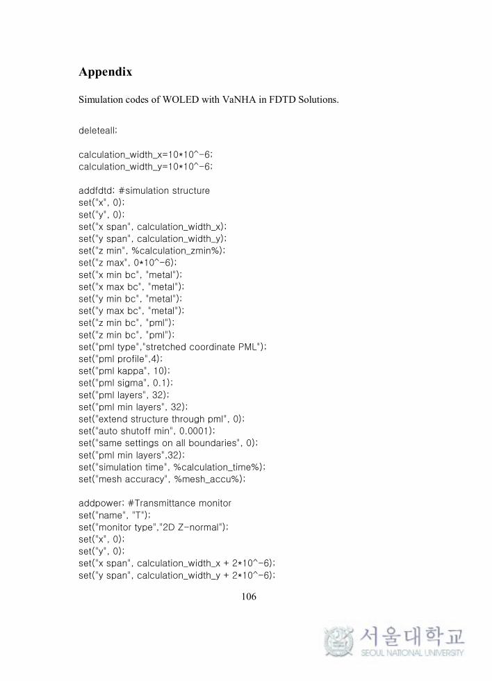
106
Appendix
Simulation codes of WOLED with VaNHA in FDTD Solutions.
deleteall;
calculation_width_x=10*10^-6;
calculation_width_y=10*10^-6;
addfdtd; #simulation structure
set("x", 0);
set("y", 0);
set("x span", calculation_width_x);
set("y span", calculation_width_y);
set("z min", %calculation_zmin%);
set("z max", 0*10^-6);
set("x min bc", "metal");
set("x max bc", "metal");
set("y min bc", "metal");
set("y max bc", "metal");
set("z min bc", "pml");
set("z min bc", "pml");
set("pml type","stretched coordinate PML");
set("pml profile",4);
set("pml kappa", 10);
set("pml sigma", 0.1);
set("pml layers", 32);
set("pml min layers", 32);
set("extend structure through pml", 0);
set("auto shutoff min", 0.0001);
set("same settings on all boundaries", 0);
set("pml min layers",32);
set("simulation time", %calculation_time%);
set("mesh accuracy", %mesh_accu%);
addpower; #Transmittance monitor
set("name", "T");
set("monitor type","2D Z-normal");
set("x", 0);
set("y", 0);
set("x span", calculation_width_x + 2*10^-6);
set("y span", calculation_width_y + 2*10^-6);

107
set("z", -500*10^-9);
set("output Ex", 1);
set("output Ey", 1);
set("output Ez", 1);
set("output Hx", 1);
set("output Hy", 1);
set("output Hz", 1);
set("output Px", 1);
set("output Py", 1);
set("output Pz", 1);
set("output power", 1);
set("override global monitor settings",1);
set("frequency points", 21);
addrect; #substrate
set("name","Substrate");
set("index",%substrate_index%); #refractive index of substrate
set("x", 0);
set("y", 0);
set("x span", calculation_width_x + 7*10^-6);
set("y span", calculation_width_y + 7*10^-6);
set("z min", -%substrate_h%);
set("z max",3*10^-6);
current_h= -%substrate_h%;
if(%include_VaNHa%==1) { #include or not include extraction layer
addrect; #SiNx
set("name","SiNx");
set("index",%SiNx_index%); #refractive index of dielectric layer
set("x", 0);
set("y", 0);
set("x span", calculation_width_x + 7*10^-6);
set("y span", calculation_width_y + 7*10^-6);
set("z max",current_h);
current_h=current_h - %SiN_h%;
set("z min", current_h);
current_h=current_h + %SiN_h% - %pc height%;
for (i=1:85) {
addcircle;
set("radius", 0.120*%scale micro%);

108
set("z min",current_h);
set("z max",current_h+%pc height%);
set("x", rand(-5,5)*%scale micro%);
set("y", rand(-5,5)*%scale micro%);
set("material", %void%);
set("name","post" + "");
set("override mesh order from material database",1);
set("mesh order",1);
addcircle;
set("radius", 0.150*%scale micro%);
set("z min",current_h);
set("z max",current_h+%pc height%);
set("x", rand(-5,5)*%scale micro%);
set("y", rand(-5,5)*%scale micro%);
set("material", %void%);
set("name","post" + "");
set("override mesh order from material database",1);
set("mesh order",1);
addcircle;
set("radius", 0.190*%scale micro%);
set("z min",current_h);
set("z max",current_h+%pc height%);
set("x", rand(-5,5)*%scale micro%);
set("y", rand(-5,5)*%scale micro%);
set("material", %void%);
set("name","post" + "");
set("override mesh order from material database",1);
set("mesh order",1);
current_h=current_h + %pc height% -%SiN_h%; }
addrect;
set("name","ITO");
set("material",%anode_material%);
set("x span",calculation_width_x + 7*10^-6);
set("y span",calculation_width_x + 7*10^-6);
set("z max",current_h);
current_h = current_h - %anode_h%;
set("z min",current_h);
addrect;
set("name","Organic");
set("material","<Object defined dielectric>");
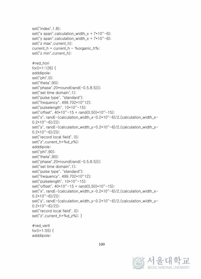
109
set("index",1.8);
set("x span",calculation_width_x + 7*10^-6);
set("y span",calculation_width_x + 7*10^-6);
set("z max",current_h);
current_h = current_h - %organic_h%;
set("z min",current_h);
#red_hori
for(i=1:126) {
adddipole;
set("phi",0);
set("theta",90);
set("phase",20*round(rand(-0.5,8.5)));
set("set time domain",1);
set("pulse type", "standard");
set("frequency", 499.702*10^12);
set("pulselength", 10*10^-15);
set("offset", 40*10^-15 + rand(0,50)*10^-15);
set("x", rand(-(calculation_width_x-0.2*10^-6)/2,(calculation_width_x-
0.2*10^-6)/2));
set("y", rand(-(calculation_width_y-0.2*10^-6)/2,(calculation_width_y-
0.2*10^-6)/2));
set("record local field", 0);
set("z",current_h+%d_z%);
adddipole;
set("phi",90);
set("theta",90);
set("phase",20*round(rand(-0.5,8.5)));
set("set time domain",1);
set("pulse type", "standard");
set("frequency", 499.702*10^12);
set("pulselength", 10*10^-15);
set("offset", 40*10^-15 + rand(0,50)*10^-15);
set("x", rand(-(calculation_width_x-0.2*10^-6)/2,(calculation_width_x-
0.2*10^-6)/2));
set("y", rand(-(calculation_width_y-0.2*10^-6)/2,(calculation_width_y-
0.2*10^-6)/2));
set("record local field", 0);
set("z",current_h+%d_z%); }
#red_verti
for(i=1:55) {
adddipole;

110
set("phi",0);
set("theta",0);
set("phase",20*round(rand(-0.5,8.5)));
set("set time domain",1);
set("pulse type", "standard");
set("frequency", 499.702*10^12);
set("pulselength", 10*10^-15);
set("offset", 40*10^-15 + rand(0,50)*10^-15);
set("x", rand(-(calculation_width_x-0.2*10^-6)/2,(calculation_width_x-
0.2*10^-6)/2));
set("y", rand(-(calculation_width_y-0.2*10^-6)/2,(calculation_width_y-
0.2*10^-6)/2));
set("record local field", 0);
set("z",current_h+%d_z%); }
#green_hori
for(i=1:52) {
adddipole;
set("phi",0);
set("theta",90);
set("phase",20*round(rand(-0.5,8.5)));
set("set time domain",1);
set("pulse type", "standard");
set("frequency", 579.123*10^12);
set("pulselength", 10*10^-15);
set("offset", 40*10^-15 + rand(0,50)*10^-15);
set("x", rand(-(calculation_width_x-0.2*10^-6)/2,(calculation_width_x-
0.2*10^-6)/2));
set("y", rand(-(calculation_width_y-0.2*10^-6)/2,(calculation_width_y-
0.2*10^-6)/2));
set("record local field", 0);
set("z",current_h+%d_z%);
adddipole;
set("phi",90);
set("theta",90);
set("phase",20*round(rand(-0.5,8.5)));
set("set time domain",1);
set("pulse type", "standard");
set("frequency", 579.123*10^12);
set("pulselength", 10*10^-15);
set("offset", 40*10^-15 + rand(0,50)*10^-15);
set("x", rand(-(calculation_width_x-0.2*10^-6)/2,(calculation_width_x-
0.2*10^-6)/2));

111
set("y", rand(-(calculation_width_y-0.2*10^-6)/2,(calculation_width_y-
0.2*10^-6)/2));
set("record local field", 0);
set("z",current_h+%d_z%); }
#green_verti
for(i=1:29) {
adddipole;
set("phi",0);
set("theta",0);
set("phase",20*round(rand(-0.5,8.5)));
set("set time domain",1);
set("pulse type", "standard");
set("frequency", 579.123*10^12);
set("pulselength", 10*10^-15);
set("offset", 40*10^-15 + rand(0,50)*10^-15);
set("x", rand(-(calculation_width_x-0.2*10^-6)/2,(calculation_width_x-
0.2*10^-6)/2));
set("y", rand(-(calculation_width_y-0.2*10^-6)/2,(calculation_width_y-
0.2*10^-6)/2));
set("record local field", 0);
set("z",current_h+%d_z%); }
#blue_hori
for(i=1:27) {
adddipole;
set("phi",0);
set("theta",90);
set("phase",20*round(rand(-0.5,8.5)));
set("set time domain",1);
set("pulse type", "standard");
set("frequency", 637.894*10^12);
set("pulselength", 15*10^-15);
set("offset", 55*10^-15 + rand(0,50)*10^-15);
set("x", rand(-(calculation_width_x-0.2*10^-6)/2,(calculation_width_x-
0.2*10^-6)/2));
set("y", rand(-(calculation_width_y-0.2*10^-6)/2,(calculation_width_y-
0.2*10^-6)/2));
set("record local field", 0);
set("z",current_h+%d_z%);
adddipole;
set("phi",90);
set("theta",90);

112
set("phase",20*round(rand(-0.5,8.5)));
set("set time domain",1);
set("pulse type", "standard");
set("frequency", 637.894*10^12);
set("pulselength", 15*10^-15);
set("offset", 55*10^-15 + rand(0,50)*10^-15);
set("x", rand(-(calculation_width_x-0.2*10^-6)/2,(calculation_width_x-
0.2*10^-6)/2));
set("y", rand(-(calculation_width_y-0.2*10^-6)/2,(calculation_width_y-
0.2*10^-6)/2));
set("record local field", 0);
set("z",current_h+%d_z%); }
#blue_verti
for(i=1:17) {
adddipole;
set("phi",0);
set("theta",0);
set("phase",20*round(rand(-0.5,8.5)));
set("set time domain",1);
set("pulse type", "standard");
set("frequency", 637.894*10^12);
set("pulselength", 15*10^-15);
set("offset", 55*10^-15 + rand(0,50)*10^-15);
set("x", rand(-(calculation_width_x-0.2*10^-6)/2,(calculation_width_x-
0.2*10^-6)/2));
set("y", rand(-(calculation_width_y-0.2*10^-6)/2,(calculation_width_y-
0.2*10^-6)/2));
set("record local field", 0);
set("z",current_h+%d_z%); }
addpower; #Transmittance monitor
set("name", "Abs");
set("monitor type","2D Z-normal");
set("x", 0);
set("y", 0);
set("x span", calculation_width_x + 2*10^-6);
set("y span", calculation_width_y + 2*10^-6);
set("z", current_h);
set("output Ex", 1);
set("output Ey", 1);
set("output Ez", 1);
set("output Hx", 1);

113
set("output Hy", 1);
set("output Hz", 1);
set("output Px", 1);
set("output Py", 1);
set("output Pz", 1);
set("output power", 1);
set("override global monitor settings",1);
set("frequency points", 21);
addrect;
set("name","Al");
set("material",%cathode_material%);
set("x", 0);
set("y", 0);
set("x span", calculation_width_x );
set("y span", calculation_width_y );
set("z max",current_h);
current_h = current_h - %cathode_h%;
set("z min",current_h);
addmesh;
set("name","mesh_OLED");
set("x", 0);
set("y", 0);
set("x span", calculation_width_x);
set("y span", calculation_width_y);
set("z max", (0.02-%substrate_h%*10^6-0.8)*10^-6);
set("dx", %mesh_x%);
set("dy", %mesh_y%);
set("dz", %mesh_OLED_z%);
addmesh;
set("name","mesh_external");
set("x", 0);
set("y", 0);
set("x span", calculation_width_x);
set("y span", calculation_width_y);
set("z min", (0.02-%substrate_h%*10^6-0.8)*10^-6);
set("z max", 1*10^-6);
set("dx", %mesh_x%);
set("dy", %mesh_y%);
set("dz", %mesh_external_z%);

114
select("FDTD");
set("z min", current_h);
current_h = current_h - 380*10^-9;
select("mesh_OLED");
set("z min", current_h);

115
Biblography
[1] S.-Y. Kim, W.-I. Jeong, C. Mayr, Y.-S. Park, K.-H. Kim, J.-H. Lee, C.-K.
Moon, W. Brütting, J.-J. Kim, Adv. Funct. Mater. 2013, 23, 3896.
[2] M. A. Baldo, D. F. O'Brien, Y. You, A. Shoustikov, S. Sibley, M. E.
Thompson, S. R. Forrest, Nature 1998, 395, 151.
[3] H. Uoyama, K. Goushi, K. Shizu, H. Nomura, C. Adachi, Nature 2012, 492,
234.
[4] C. K. Chiang, C. R. Fincher, Jr., Y. W. Park, A. J. Heeger, H. Shirakawa, E.
J. Louis, S. C. Gau, A. G. MacDiarmid, Phys. Rev. Lett. 1977, 39, 1098.
[5] J.-H. Lee, J.-J. Kim, Phys. Status Solidi A 2012, 209, 1399.
[6] I. D. Parker, J. Appl. Phys. 1993, 75, 1656.
[7] P. A. Hobson, S. Wedge, J. A. E. Wasey, I. Sage, W. L. Barnes, Adv. Mater.
2002, 14, 193.
[8] P. T. Worthing. W. L. Barnes, Appl. Phys. Lett. 2001, 29, 3035.
[9] C. F. Madigan, M. H. Lu, J. C. Sturm, Appl. Phys. Lett. 2000, 76, 1650.
[10] T. Tsutsui, M. Yashiro, H. Yokogawa, K. Kawano, M. Yokoyama, Adv.
Mater. 2001, 13, 1149.
[11] L. H. Smith, J. A. Wasey, W. L. Barnes, Appl. Phys. Lett. 2004, 84, 2986.
[12] S. Möller, S. R. Forrest, J. Appl. Phys. 2002, 91, 3324.
[13] Y. Sun, S. R. Forrest, J. Appl. Phys. 2006, 100, 073106.
[14] J.-B. Kim, J.-H. Lee, C.-K. Moon, S.-Y. Kim, J.-J. Kim, Adv. Mater. 2013,
25, 3571.

116
[15] B. W. D’Andrade, J. J. Brown, Appl. Phys. Lett. 2006, 88, 192908.
[16] T. Yamasaki, K. Sumioka, T. Tsutsui, Appl. Phys. Lett. 2000, 76, 1243.
[17] J. J. Shiang, T. J. Faircloth, Anil R. Duggal, J. Appl. Phys. 2004, 95, 2889.
[18] Y. H. Kim, J. Lee, W. M. Kim, C. Fuchs, S. Hofmann, H.-W. Chang, M. C.
Gather, L. Müller-Meskamp, K. Leo, Adv. Funct. Mater. 2014, 24, 2553.
[19] C.-H. Shin, E. Y. Shin, M.-H. Kim, J.-H. Lee, Y. Choi, Opt. Express 2015,
23, A133.
[20] E. Kim, H. Cho, K. Kim, T.-W. Koh, J. Chung, J. Lee, Y. Park, S. Yoo,
Adv. Mater. 2015, 27, 1624.
[21] S. Reineke, F. Lindner, G. Schwartz, N. Seidler, K. Walzer, B. Lu¨ssem, K.
Leo, Nature, 2009, 459, 234.
[22] S. Mladenovski, K. Neyts, D. Pavicic, A. Werner, C. Rothe, Opt. Express
2009, 17, 7562.
[23] Y.-H. Cheng, J.-L. Wu, C.-H. Cheng, K.-C. Syao, M.-C. M. Lee, Appl.
Phys. Lett. 2007, 90, 091102.
[24] S. Chen, H. S. Kwok, Opt. Express 2010, 18, 37.
[25] Y.-J. Lee, S.-H. Kim, J. Huh, G.-H. Kim, Y.-H. Lee, S.-H. Cho, Y.-C. Kim,
Y. R. Do, Appl. Phys. Lett. 2003, 82, 3779.
[26] S. Jeon, J.-W. Kang, H.-D. Park, J.-J. Kim, J. R. Youn, J. Shim, J.-H. Jeong,
D.-G. Choi, K.-D. Kim, A. O. Altun, S.-H. Kim, Y.-H. Lee, Appl. Phys. Lett.
2008, 92, 223307.
[27] S. Jeon, J.-H. Jeong, Y. S. Song, W.-I. Jeong, J.-J. Kim, J. R. Youn,
Nanoscale, 2014, 6, 2642.

117
[28] S. Jeon, J.-H. Lee, J.-H. Jeong, Y. S. Song, C,-K. Moon, J.-J. Kim, J. R.
Youn, Sci. Rep. 2015, 5, 8865.
[29] C. Lee, J.-J. Kim, Small, 2013, 9, 3858.
[30] J.-W. Shin, D.-H. Cho, J. Moon, C. W. Joo, S. K. Park, J. Lee, J.-H. Han,
N. S. Cho, J. Hwang, J. W. Huh, H. Y. Chu, J.-I. Lee, Org. Electronics, 2014,
15, 196.
[31] Y. Sun, S. R. Forrest, Nat. Photonics 2008 2, 483.
[32] J. Choi, T.-W. Koh, S. Lee, S. Yoo, Appl. Phys. Lett. 2012, 100, 233303.
[33] L. Zhou, Q.-D. Ou, Y.-Q. Li, H.-Y. Xiang, L.-H. Xu, J.-D. Chen, C. Li, S.
Shen, S.-T. Lee, J.-X. Tang, Adv. Funct. Mater. 2015, 25, 2660.
[34] Q.-D. Ou, L. Zhou, Y.-Q. Li, S. Shen, J.-D. Chen, C. Li, Q.-K. Wang, S.-T.
Lee, J.-X. Tang, Adv. Funct. Mater. 2014, 24, 7249.
[35] L. Li, J. Liang, S.-Y. Chou, X. Zhu, X. Niu, Z. Yu, Q. Pei, Sci. Rep. 2014,
4, 4307.
[36] A. O. Altun, S. Jeon, J. Shim, J.-H. Jeong, D.-G. Choi, K.-D. Kim, J.-H.
Choi, S.-W. Lee, E.-S. Lee, H.-D. Park, J. R. Youn, J.-J. Kim, Y.-H. Lee, J.-W.
Kang, Org. Electronics, 2010, 11,711.
[37] W. H. Koo, S. M. Jeong, F. Araoka, K. Ishikawa, S. Nishimura, T.
Toyooka, H. Takezoe, Nature Photon. 2010, 4, 222.
[38] Y.-G. Bi, J. Feng, Y.-F. Li, X.-L. Zhang, Y.-F. Liu, Y. Jin, H.-B. Sun, Adv.
Mater. 2013, 25, 6969.
[39] W. Youn, J. Lee, M. Xu, R. Singh, F. So, ACS Appl. Mater. Interfaces,
2015, 7, 8974.

118
[40] C.-L. Lin, H.-W. Lin, C.-C. Wu, Appl. Phys. Lett. 2005, 87 021101.
[41] C.-J. Yang, S.-H. Liu, H.-H. Hsieh, C.-C. Liu, T.-Y. Cho, C.-C. Wu, Appl.
Phys. Lett. 2007, 91 253508.
[42] K.-H. Kim, J.-L. Liao, S. W. Lee, B. Sim, C.-K. Moon, G.-H. Lee, H. J.
Kim, Y. Chi, J.-J. Kim, Adv. Mater. 2016, 28, 2526.
[43] K.-H. Kim, E. S. Ahn, J.-S. Huh, Y.-H. Kim, J.-J. Kim, Chem. Mater. 2016,
28, 7505.
[44] H. Shin, J.-H. Lee, C.-K. Moon, J.-S. Huh, B. Sim, J.-J. Kim, Adv. Mater.
2016, 28, 4920.
[45] J.-H. Lee, S. Lee, J.-B. Kim, J. Jang, J.-J. Kim, J. Mater. Chem. 2012, 22,
15262.
[46] Y.-H. Huang, C.-Y. Lu, S.-T. Tsai, Y.-T. Tsai, C.-Y. Chen, W.-L. Tsai, C.-
Y. Lin, H.-W. Chang, W.-K. Lee, M. Jiao, C.-C. Wu, Appl. Phys. Lett. 2014,
104, 183302.
[47] K. Yee, IEEE Trans. Antenn. Propag. 1966, 14, 302.
[48] A. Chutinan, K. Ishihara, T. Asano, M. Fujita, S. Noda, Org. Electronics
2005, 6, 3.
[49] Y.-J. Lee, S.-H. Kim, G.-H. Kim, Y.-H. Lee, S.-H. Cho, Y.-W. Song, Y.-C.
Kim, Y. R. Do, Opt. Express 2005, 13, 5864.
[50] J. Adam, J. Hauss, S. Gleiss, B. Riedel, U. Geyer, U. Lemmer, M. Gerken,
ICTON-MW 2009. 3rd 2009, 1.
[51] Q. Yue, W. Li, F. Kong, K. Li, Adv. Mater. Sci. Eng. 2012, 2012, 985762.
[52] J.-W. Kim, J.-H. Jang, M.-C. Oh, J.-W. Shin, D.-H. Cho, J.-H. Moon, J.-I.

119
Lee, Opt. Express 2014, 22, 498.
[53] M. K. Callens, H. Marsman, L. Penninck, P. Peeters, H. d. Groot, J. M. t.
Meulen, K. Neyts, Opt. Express 2014, 22, A589.
[54] J.-G. Kim, C.-H. Hsieh, H. J. Choi, J. Gardener, B. Singh, A. Knapitsch, P.
Lecoq, G. Barbastathis, Opt. Express 2015, 23, 22730.
[55] J.-B. Kim, J.-H. Lee, C.-K. Moon, K.-H. Kim, J.-J. Kim, Org. Electronics
2015, 17, 115.
[56] W. Wang, H. Peng, S. Wang, S. Chen, Org. Electronics 2015, 24, 195.
[57] Y. Qu, C. Coburn, D. Fan, S. R. Forrest, ACS Photonics 2017, 4, 363.
[58] D. Englund, D. Fattal, E. Waks, G. Solomon, B. Zhang, T. Nakaoka, Y.
Arakawa, Y. Yamamoto, J. Vucˇkovic´, Phys. Rev. Lett. 2005, 95, 013904.
[59] P. T. Kristensen, C. Van Vlack, S. Hughes, Opt. Letters 2012, 37, 1649.
[60] Lumerical Solutions, Inc. http://www.lumerical.com/tcad-products/fdtd/.
[61] R. R. Chance, A. Prock, R. Silbey, Adv. Chem. Phys. 1987, 37, 1.
[62] S. Kim, J.-J. Kim, Org, Electronics 2010, 11, 1010.
[63] C.-K. Moon, S.-Y. Kim, J,-H. Lee, J.-J. Kim, Opt. Express 2015, 23, A279.
[64] J. D. Jackson, John Wiley & Sons, Inc. 1999, 3rd edition.
[65] C.-C. Ma, Y.-J. Chen, L.-J. Hsiao, Proc. SPIE 9137 Organic Photonics VI
2014, 91370J.
[66] M. C. Gather, S. Reineke, J. Photon. Energ. 2015, 5, 057607.
[67] H. -W. Chang, J. Lee, S. Hofmann, Y. H. Kim, L. Müller-Meskamp, B.
Lüssem, C. -C. Wu, K. Leo, M. C. Gather, J. Appl. Phys. 2013, 113, 204502.
[68] H. -W. Chang, Y. H. Kim, J. Lee, S. Hofmann, B. Lüssem, L. Müller-

120
Meskamp, M. C. Gather, K. Leo, C. -C. Wu, Org. Electron. 2014, 15, 1028.
[69] P. E. Burrows, S. R. Forrest, L. S. Sapochak, J. Schwartz, P. Fenter, T.
Buma, V. S. Ban, J. L. Forrest, J. Cryst. Growth 1995, 156, 91.
[70] M. Baldo, M. Deutsch, P. Burrows, H. Gossenberger, M. Gerstenberg, V.
Ban,S. Forrest, Adv. Mater. 1998, 10, 1505.
[71] M. A. Baldo, V. G. Kozlov, P. E. Burrows, S. R. Forrest, V. S. Ban, B.
Koene, M. E. Thompson, Appl. Phys. Lett. 1997, 71, 3033.
[72] S. C. Seel, C. V. Thompson, J. Appl. Phys. 2003, 93, 9038.
[73] S. Lee, Orange and White Organic light Emitting Diodes using Exciplex-
forming Co-hosts, PhD dissertation, Seoul National University, 2014.
[74] K.-H. Kim, C.-K. Moon, J.-H. Lee, S.-Y. Kim, J.-J. Kim, Adv. Mater. 2014,
26, 3844.
[75] K.-H. Kim, S. Lee, C.-K. Moon, S.-Y. Kim, Y.-S. Park, J.-H. Lee, J. W.
Lee, J. Huh, Y. You, J.-J. Kim, Nat. Commun. 2014, 5, 4769.
[76] H. Shin, S. Lee, K.-H. Kim, C.-K. Moon, S.-J. Yoo, J.-H. Lee, J.-J. Kim,
Adv. Mater. 2014, 26, 4730.
[77] H. Sasabe, J. Takamatsu, T. Motoyama, S. Watanabe, G. Wagenblast, N.
Langer, O. Molt, E. Fuchs, C. Lennartz, J. Kido, Adv.Mater. 2010, 22, 5003.
[78] W. Gaynor, S. Hofmann, M. G. Christoforo, C. Sachse, S. Mehra, A.
Salleo, M. D. McGehee, M. C. Gather, B. Lüssem, L. Müller-Meskamp, P.
Peumans, K. Leo, Adv. Mater. 2013, 23, 4006.
[79] N. Li, S. Oida, G. S. Tulevski, S.-J. Han, J. B. Hannon, D. K. Sadana, T.-C.
Chen, Nature Comm. 2013, 4, 2294.

121
[80 N. Ide, K. Yamae, V. Kittichungchit, H. Tsuji, M. Ota, T. Komoda, J.
Photopolym. Sci. Technol. 2014, 27, 357.
[81] K. Kato, T. Iwasaki, T. Tsujimura, J. Photopolym. Sci. Technol. 2015, 28,
335.
[82] D. Riedel, T. Wehlus, T. C.G. Reusch, C. J.Brabec, Org. Electronics, 2016,
32, 27.
[83] M. Du, Y. Feng, D. Zhu, T. Peng, Y. Liu, Y. Wang, M. R. Bryce, Adv.
Mater. 2016, 28, 5963.
[84] J. Kido, M. Kimura, K. Nagai, Science 1995, 267, 1332.
[85] J. Ye, C.-J. Zheng, X.-M. Ou, X.-H. Zhang, M.-K. Fung, C.-S. Lee, Adv.
Mater. 2012, 24, 3410.
[86] T. Fleetham, J. Ecton, Z. Wang, N. Bakken, J. Li, Adv. Mater. 2013, 25,
2573.
[87] K. Udagawa, H. Sasabe, F. Igarashi, J. Kido, Adv. Mater. 2016, 4, 86.
[88] X. Zhuang, H. Zhang, K. Ye, Y. Liu, Y. Wang, ACS Materials &
Interfaces 2016, 8, 11221.
[89] A. R. Duggal, J. J. Shiang, C. M. Heller, D. F. Foust, Appl. Phys. Lett.
2002, 80, 3470.
[90] S. Krotkus, D. Kasemann, S. Lenk, K. Leo, S. Reineke, Light: Sci. Appl.
2016, 5, e16121.
[91] C.-C. Chang, J.-F. Chen, Appl. Phys. Lett. 2005, 87, 253501.
[92] S. Lee, H. Shin, J.-J. Kim et al., Adv. Mater. 2014, 26, 5864.
[93] H. Cho, C. W. Joo, J. Lee, H. Lee, J. Moon, J.-I. Lee, J. Y. Lee, Y. Kang, N.

122
S. Cho, Opt. Express 2016, 24, 24161.
[94] C. Coburn, C. Jeong, S. R. Forrest, ACS Photonics 2017, 10.1021.
[95] S. Lee, J.-H. Lee, J.-H. Lee, J.-J. Kim, Adv. Funct. Mater. 2012, 22, 855
[96] Y.Ohno, Energy Star Webinar March 2016.
[97] L. Ding, S.-C. Dong, Z.-Q. Jiang, H. Chen, L.-S. Liao, Adv. Funct. Mater.
2015, 25, 645.
[98] Z. T. Zhang, S.-J. He, D.-K. Wang, N. J.iang, Z.-H. Lu, Sci. Rep. 2016, 6,
20517.
[99] X.-L. Li, G. Xie, M. Liu, D. Chen, X. Cai, J. Peng, Y. Cao, S.-J. Su, Adv.
Mater. 2016, 28, 4614.
[100] J. M. Choi, D. R. Lee, J. Y. Lee, Dyes and Pigments 2017, 142, 243.
[101] K.-H. Kim, J.-Y. Ma, C.-K. Moon, J.-H. Lee, J. Y. Baek, Y.-H. Kim, J.-J.
Kim, Adv. Opt. Mater. 2015, 3, 1191.
[102] J. H. Seo, G. Y. Kim, J. H. Kim, J. S. Park, B. M. Seo, K. H. Lee, S. S.
Yoon, Y. K. Kim, J. J. Appl. Phys. 2009, 48, 082103.
[103] H. Lim, H. Shin, K.-H. Kim, S.-J. Yoo, J.-S. Huh, J.-J. Kim, ACS Applied
Materials & Interfaces 2017, 9, 37883.

123
초 록
유기발광소자는 최근 차세대 디스플레이 및 조명용 발광소자로 각광
받고 있다. 유기발광소자가 산업계 전반에 사용되기 위해서,
광추출효율이 더욱 개선될 필요가 있다. 디스플레이용 광추출을 하기
위해서 높은 광추출효율 향상량, 시야각에 따른 낮은 스펙트럼 변화,
낮은 픽셀 빛번짐 및 높은 명암비가 요구된다. 그리고, 전면발광형
유기발광소자의 상부전극에 피해를 주지않는 공정방법이 요구된다.
조명용 광추출을 하기 위해서 높은 광추출효율 향상량, 낮은 시야각에
따른 스펙트럼 변화, 균일한 발광분포 및 높은 색품질이 요구된다.
조명은 보통 배면발광형을 사용하기 때문에 다양한 공정을 적용할 수
있지만 무기발광소자 및 다른 광원들과 경쟁해야하기 때문에 높은
광추출효율 향상량이 요구된다.
광추출효율을 향상시키기 위해서 마이크로렌즈어레이, 광결정,
산란층, 주름구조가 적용된 소자 등등 다양광 방법들이 보고되었다. 그
중, 진공증착법으로 유기물 마이크로렌즈어레이를 제작하는 방법이 제작
중 소자에 피해를 주지 않는 점과, 높은 광추출효율 향상 및 낮은
스펙트럼 변화 등의 이유로 디스플레이용 광추출구조물의 가능성을
가지고 있다. 그러나 실제 디스플레이 공정의 제조시간을 맞추기

124
위해서는 광추출구조물의 크기가 작아질 필요가 있다. 게다가, 구조물의
크기를 줄일 경우에는 이를 최적화하는 정교한 모델링이 필요하다.
조명용 광추출구조로선 진공홀어레이가 평탄한 표면에 의한 전기적
안정성, 반구렌즈와 함께 했을 때 높은 광추출 등의 이유로 가능성을
보인다. 육각분포의 진공나노구멍구조가 에어모드, 기판모드,
웨이브가이드모드를 전부 추출하는 보고가 있었지만, 균일한 발광분포가
필수적인 조명에서는 적용하기 힘들다는 단점이 있다.
이번 학위 논문에서는 위의 두가지 주제 (1) 디스플레이용 유기물
나노렌즈어레이가 적용된 전면발광형 유기발광소자의 광추출효율과 (2)
조명용 진공구멍어레이가 적용된 소자의 광추출효율 및 색 품질을
다룬다. 이번 논문에서 위의 두 방법이 각각 조명과 디스플레이
실용적으로 적용할 수 있는 방법임을 보일 것이다.
학위 논문은 디스플레이와 조명으로 크게 나뉘어지며, 본론에 앞서
1장에서는 유기발광소자의 효율, 광손실경로, 광추출방법 및
유한차분법에 대해 간단한 소개를 담았다.
2장에서 광추출구조가 적용된 상부발광형 유기발광소자의
광추출효율을 유한차분법으로 계산하는 방법을 담았다. 유한차분법을
사용할 때에 있어 계산 변수들의 영향에 대해서 먼저 다룬다. 최적화된
계산 변수들을 검증하기위해 고전전자기모델링으로 계산한 퍼셀인자와
광추출효율을 비교하였고, 계산 결과의 차이가 거의 없음을 확인하였다.

125
이를 바탕으로 유기나노렌즈어레이가 적용된 소자의 광추출효율을
계산한 결과를 정리하였다.
3장에서, 유기나노렌즈어레이로 인한 광추출효율 향상에 대해
다룬다. 임의분포를 가지는 유기나노렌즈어레이는 유기증기물리증착법을
통해 제작할 수 있다. 제작된 유기나노렌즈어레이의 구조들을
유한차분법으로 계산하여 높은 광추출효율을 가지는 분포를 제시하였다.
또한 광추출구조물이 유기물보다 더 높은 물질로 이루어질 경우에
광추출효율 향상량이 더 높아짐을 계산으로 확인하였다.
산화물인듐아연을 상부전극으로 사용한 전면발광형 소자에
유기물리증착법을 사용하여 렌즈어레이를 만들고 녹색, 청색 소자를
제작하였다. 두 소자 모두 50%이상의 광추출효율 향상량을 보였으며,
계산에서 얻은 향상량과 일치했다.
4장에선, 진공나노구멍구조를 임의적으로 분포시킨 후 백색
유기발광소자에 적용한 것에 대해 다룬다. 이때 외부양자효율은 78%,
전력효율은 164 lm/W라는 현재까지 보고된 값 중 가장 높은 값을
가지는 결과이다. 임의분포를 형성하기 위해 반지름이 각각 120, 150,
190 nm인 나노홀을 임의숫자생성함수를 사용하여 분포시켰다. 기판의
바깥쪽에 반구렌즈를 적용하여 공기, 기판, 웨이브가이드 모드를 전부
추출할 수 있었다. 임의분포 덕분에 백색 소자의 시야각에 따른
스펙트럼 변화는 거의 없었고, 균일한 발광 패턴을 가지는 소자가

126
제작되었다. Si3N4와 공기로 이루어진 광추출 구조물의 높은 광추출효율
향상량의 기원을 파악하기 위해 FDTD 계산을 하였다. 유전층과 nano
hole array의 굴절률 차이가 클수록, 광추출 효율이 크며 내부에
waveguide가 거의 추출되는 것을 알 수 있었다.
5장에서 다양한 광추출구조가 적용되었을 때 이론적으로 얻을 수
있는 탠덤 백색소자의 색 품질에 대해 다룬다. 먼저 염료들의 비율에
따른 PL 스펙트럼 합이 가지는 색 품질을 계산하여 색 좌표에 따른
연색성을 계산하였다. 다음으로 마이크로 공진구조를 감안하여,
광추출구조가 없는 소자, 반구렌즈가 적용된 소자, 고굴절 기판과
고굴절 반구렌즈가 적용된 소자 및 고굴절 기판과 고굴절 반구렌즈와
두꺼운 전자수송층이 적용된 소자가 가지는 색 품질을 계산하였다.
마이크로 공진구조가 강할수록 청색 염료의 두번째 픽의 크기가
감소하고, PL로 얻을 수 있는 최종 색 품질과의 차이가 커지는 것을
발견했다. 모델링에 대한 검증을 위해 고효율 탠덤 백색소자를 제작하여
반구렌즈 유무에 따른 스펙트럼을 비교하였고, 스펙트럼 비율을 잘
추적하는 것을 확인하였다. 이때 제작된 소자는 6500 K 이상의 높은
색온도를 가지며 38 lm/W의 전력 효율 및 80 이상의 연색성을 가지는
고품질 소자가 구현되었다.
주요어: 유기발광소자, 광추출, 상부발광형 유기발광소자,

127
유기발광소자 조명, 유한차분법, 몬테-칼로, 주기격자이론
학번: 2013-30767

128
CURRICULUM VITAE
Kyung-Hoon Han
Department of Materials Science and Engineering
Seoul National University, Seoul, 151-744, Korea
+82-2-875-2412 (Office)
E-mail: [email protected]
Education
2013.03 ~ 2018.02 Ph.D. in Materials Science and Engineering
Supervisor: Professor Jang-Joo Kim
Seoul National University, Seoul, Korea
2011.03 ~ 2013.02 M.S. in Materials Science and Engineering
Supervisor: Professor Jang-Joo Kim
Seoul National University, Seoul, Korea
2007.03 ~ 2011.02 B.S. in Materials Science and Engineering
Seoul National University, Seoul, Korea
Research Interests
Organic light-emitting diodes, light extraction efficiency, finite difference time
domain method, display, lighting, color quality, computational electromagnetics
Professional Skills
− Design and fabrication of organic electronic devices: Thermal evaporator,
Glove-box, Spin coater

129
− The optoelectronic analyses on organic semiconductors: UV-vis-NIR
absorption spectroscopy, OLEDs characteristic measurements, Angle
dependent EL analysis
− The structural characterization of organic semiconductors: AFM, α-STEP
− Finite difference time domain calculations
− Rigorous coupled wave analysis calculations
− Ray tracing calculations
Scholarship and Fellowship
− Brain Korea 21 Scholarship (2011.03~)
− World Class University (WCU) project through National Research Foundation
of Korea funded by the Ministry of Education, Science and Technology
(2011.03~)

130
List of Publications
1. Yang Doo Kim(+), Kyung-Hoon Han(+), Sang-Jun Park, Jung-Bum Kim, Ju-
Hyeon Shin, Jang Joo Kim, and Heon Lee, "Enhanced light extraction
efficiency in organic light emitting diodes using a tetragonal photonic crystal
with hydrogen silsesquioxane", Opt. Lett. 2014, 39, 5901.
2. Yang Doo Kim(+), Kyung-Hoon Han(+), Young Hoon Sung, Jung-Bum Kim,
Hak-Jong Choi, Heon Lee, Jang-Joo Kim, "Enhanced light extraction
efficiency in organic light-emitting diode with randomly dispersed
nanopattern", Opt. Lett. 2015, 40, 5838.
3. Cholho Lee, Kyung-Hoon Han, Kwon-Hyeon Kim, Jang-Joo Kim, "Direct
formation of nano-pillar arrays by phase separation of polymer blend for the
enhanced out-coupling of organic light emitting diodes with low pixel
blurring", Opt. Express 2016, 24, A488.
4. Young-Sam Park(+), Kyung-Hoon Han(+), Jehan Kim, Doo-Hee Cho, Jonghee
Lee, Yoonjay Han, Jong Tae Lim, Nam Sung Cho, Byounggon Yu, Jeong-Ik
Lee, Jang-Joo Kim, "Crystallization-assisted nano lens array fabrication for
highly efficient and color stable organic light emitting diodes", Nanoscale
2017, 9, 230.
5. Young Hoon Sung(+), Pil-Hoon Jung(+), Kyung-Hoon Han, Yang Doo Kim,
Jang-Joo Kim, Heon Lee, "Improved out-coupling efficiency of organic light

131
emitting diodes fabricated on a TiO2 planarization layer with embedded Si
oxide nanostructures", Optical Materials 2017, 72, 828.
6. Young Hoon Sung, Kyung-Hoon Han, Yang Doo Kim, Yoonjay Han, Jang-Joo
Kim, Heon Lee, "Air void optical scattering structure for high-brightness
organic light emitting diodes", Ceramics International 2017, 43, S455.

132
List of Presentations
International Conference
1. Kyung-Hoon Han, Yang-Doo Kim, Young-Hoon Sung, Jung-Bum Kim, Hak-
Jong Choi, Heon Lee, Jang-Joo Kim, "Enhanced Light Extraction Efficiency
in Organic Light-emitting Diode with Randomly Dispersed Nanopattern", A-
COE2015, October 29-31 (October 30), 2015, China (Poster)
2. Kyung-Hoon Han, Yang-Doo Kim, Young-Hoon Sung, Jung-Bum Kim, Hak-
Jong Choi, Heon Lee, Jang-Joo Kim, "Enhanced light extraction efficiency in
organic light-emitting diode with randomly dispersed nanopattern", The 7th
International Workshop on Flexible & Printable Electronics 2015 (IWFPE
2015), November 4-6 (November 5), 2015, Korea (Poster)
3. Cholho Lee, Kyung-Hoon Han, Kwon-Hyeon Kim, Jang-Joo Kim, "Direct
formation of nano-pillar arrays by phase separation of polymer blend for the
enhanced out-coupling of organic light emitting diodes with low pixel
blurring", The International Symposium on Recent Advanes and Future Issues
in Organic Electroluminscence (ISOEL2016), February 17-19 (February 18),
2016, Korea (Poster)
4. Young-Sam Park, Kyung-Hoon Han, Doo-Hee Cho, Jonghee Lee, Yoon-Jay
Han, Nam Sung Cho, Byoung-Gon Yu, Jang-Joo Kim, Jeong-Ik Lee,
"Maskless Integration of Nano Lens Arrays (NLAs) on Inverted Top Emitting
Organic Light Emitting Diodes (TEOLEDs) for High Light Extraction

133
Efficiency", OSA Light, Energy & Environment Congress, November 14-17
(November 16), 2016, Germany (Poster)
5. Sohee Jeon, Sunghun Lee, Kyung-Hoon Han, Hyun Shin, Kwon-Hyeon Kim,
Jun-Ho Jeong, Jang-Joo Kim, "High Quality White OLEDs with Comparable
Efficiencies to LEDs using randomly dispersed vacuum nanohole array", The
28th Internaional Conference on Molecular Electronics and Devices 2017 (IC
ME&D 2017), May 18-19 (May 18), 2017, Korea (Poster)
6. Kyung-Hoon Han, Sohee Jeon, Sunghun Lee, Kwon-Hyeon Kim, Hyun Shin,
Jun-Ho Jeong, Jang-Joo Kim, "High quality white OLEDs with LED
efficiencies", SPIE Optics+Photonics 2017, August 6-10 (August 6), 2017,
USA (Poster)
7. Young-Sam Park, Kyung-Hoon Han, Doo-Hee Cho, Jehan Kim, Byouggon
Yu, Nam Sung Cho, Jang-Joo Kim, Jeong-Ik Lee, "A Nano-lens Array
Fabrication Using a Mask-free Deposition for Highly Efficient and Pixel Blur-
free Top-emitting OLEDs", The 17th International Meeting on Information
Display (iMiD 2017), August 28-31 (August 31), 2017, Korea (Oral)
8. Sohee Jeon, Sunghun Lee, Kyung-Hoon Han, Hyun Shin, Kwon-Hyeon Kim,
Jun-Ho Jeong, Jang-Joo Kim, "Optical Analysis of White Organic Light
Emitting Diodes with Randomly Dispersed Nano-pillar Array", The 17th
International Meeting on Information Display (iMiD 2017), August 28-31
(August 31), 2017, Korea (Poster)
134
Domestic Conference
1. 한경훈, 김장주, "Enhanced light extraction efficiency of organic light
emitting diodes using hydrogen silsesquoxane nano-pillar arrays", 2013
한국고분자학회 춘계학술대회, April 11-12, 2013 (Poster)
2. 한경훈, 이철호, 김장주, "The Enhanced Out-Coupling of Organic Light
Emitting Diodes with Low Haze using Nano Pillar Arrays Directly
Formed by Phase Separation of Polymer Blend", 2014 Materials Fair,
September 25, 2014, Korea (Poster)
3. 한경훈, 김장주, "Direct formation of nano-pillar arrays by phase
separation of polymer blend for the enhanced out-coupling of organic light
emitting diodes with low pixel blurring", 2016 한국고분자학회
춘계학술대회, April 6-8 (April 8), 2016, Korea (Poster)