dio_en
DESCRIPTION
descdioTRANSCRIPT

FSBUS
IO

Input / Output
IO
FSBUS
Dirk Anderseck
2 von 30
Impressum The electronic, software and this manual were designed by Dirk Anderseck. All rights reserved. Reproductions of every type require the written approval of the editor. These instructions correspond to the technical stand at printing. Subject to alterations.
© Copyright 2000-2005 Dirk Anderseck
[email protected] The FSBUS wirings and software are freely available for private use. A commercial use of the wirings, software or parts of it, requires a written approval by the owner Dirk Anderseck. Please contact me at [email protected].
History Sep. 2005 Preliminary version
Oct. 2005 Added Pony-Prog description for device setup

Input / Output
IO
FSBUS
Dirk Anderseck
3 von 30
Operating conditions The operation of the assembly is provided for hobby applications in the interior. All consumers attached directly at the FSBUS cable may not exceed a current consumption of altogether 2 amps. The permitted environmental temperature may not exceed 0° degrees Celsius and 40° degrees Celsius. The device is meant for the use in dry and clean rooms. The assemblies may be taken only under supervision of an informed adult or an expert into operation!
Safety Tools only may be used if you guarantee that the equipment is separated from the supply tension and electrical charges which are stored in the components situated in the device were unloaded before. I particularly hereby point out that FSBUS components only should be built by experienced electronics technicians. I dissociate myself from possible damages which can arise. All operation is carried out at your own risk.

Input / Output
IO
FSBUS
Dirk Anderseck
4 von 30
IO Controller This IO controller is a multipurpose microcontroller driven electronic component based on ATMEL 8535 processor. You can attach switches, buttons, rotaries, lamps, analog meters, potentiometers and other equipment. Each event on one of the inputs is sent via an attached COM board to the fsbus router software. You may send commands, configuration and data from fsbus router to a specific output port on this controller.
(This photo is a beta prototype. The final layout will have a few changes.)
Features of ATMEGA 8535 • High-performance, Low-power AVR® 8-bit Microcontroller • 16 MIPS Throughput at 16 MHz • Nonvolatile Program and Data Memories • 8K Bytes of In-System Self-Programmable Flash • In-System Programming by On-chip Boot Program • True Read-While-Write Operation • 512 Bytes EEPROM • Endurance: 100,000 Write/Erase Cycles • 512 Bytes Internal SRAM • 8-channel, 10-bit ADC • Programmable Serial USART • 32 Programmable I/O Lines
Input / Output
IO
FSBUS
Dirk Anderseck
5 von 30
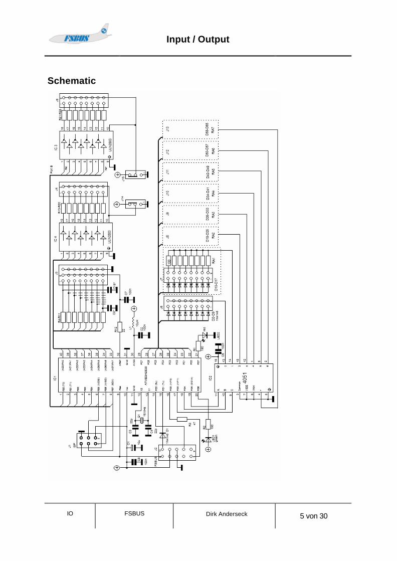
Schematic
Input / Output
IO
FSBUS
Dirk Anderseck
6 von 30
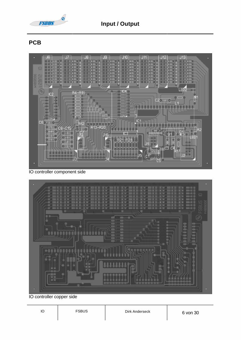
PCB
IO controller component side
IO controller copper side

Input / Output
IO
FSBUS
Dirk Anderseck
7 von 30
Microcontroller section The heart of the IO board is a microcontroller ATMEGA8535 which is driven by a 16Mhz chrystal. Connection blocks for FSBUS (10pin) and a compatible ISP adapter (6pin) as well as a few capacitors builds the core of the controller.
Diagnostic LED A green and a red led mounted on the pcb indicate several states. After power on and reset, the green LED shows the configured CID (Controller ID). Before you set the CID with fsadmin, the default value of 31 is shown. The 3 is displayed as 3 long blips in sequence and the 1 is shown as 1 short blip. Short red blips show a transmission process to the PC. Long red blips shows an error situation, which may appear, if fsbus router sends an illegal command to this controller. Short green blips indicates a receive dataframe from fsbus router. Only commands directed addressed to this controller are shown.
Reset A reset is caused by different events.
• Power On • Low on FSBUS pin 9 • Software command 128 • Configuration commands
In any case, the initialization function rereads the internal EEPROM and resets the internal states. The controller then sends some information to fsbus router:
• Reset occurred, version number of firmware • Current analogue output portbits on port A • Current analogue input portbits on port A • The 8 analogue tolerance values
The first information causes the fsbus router to resend output state. This gets LED’s shining, which shined before the reset. The other informations are used by fsadmin to update the controls of the windows program.
Input / Output
IO
FSBUS
Dirk Anderseck
8 von 30
Key section The keys section consists of a CMOS multiplexer 4051 and 8 16pin terminal blocks to connect up to 64 simple keys. Rotaries, UpDown buttons require 2 inputs which reduces the amount of attachable keys to 32 (you can mix different types of switches). Each key different from a simple on/off button needs to be configured by fsadmin software. The keytypes as well as all other configuration are stored in the internal EEPROM of the microcontroller. The key inputs are decoupled by 1N4148 diodes. You can either use ordinary or SMD parts. RA1-RA7 are resistor arrays. They can be substituted by simple wires, but its easier to use the arrays.
Key types FSBUS IO controller is designed to support the keys, switches and buttons used in a homemade flightdeck. It was a surprising experience for me, how different many of those are. The big challenge are the rotary switches. Each kind requires its own software algorithms to decode the turn direction. The key interface has connection blocks for up to 64 keys with 1 line input (on/off switch). The software numbers these keys from 0 to 64. If a button is pressed down, the software will send a dataframe containing the CID (controller id), key number and 1 or 0 for up or down. When the button is released, a second dataframe with the up-value (0 or 1) will be sent. The rotaries are connected with more than 1 input line. Before using those, you must setup the controller by sending a configuration command with keytype and keynumber. The keytype also defines how many lines are occupied by this key. If you do not define a keytype, the input line will be decoded as a simple button. When a rotary is turned, the value sent by controller is a positive or negative value for right or left turns. The value is in most cases a 1 or -1, but if turning faster than the controller can send, it will be a value greater 1.

Input / Output
IO
FSBUS
Dirk Anderseck
9 von 30
In version 1 the implemented keytypes are: 1 On/off button or switch
2 Ordinary modified 4 stage rotary switch with 4 input lines and 1 common line
3 Up/down rotary switch with 2 input lines and 1 common line. This key closes one switch on right turn step and the other switch on left turn step.
4 Two phase rotary with 2 input lines and 1 common line. At each step, the open or closed state of one pin at the moment of closing edge on the other pin determines the direction.
5 Two phase rotary with 2 input lines and 1 common line. At each step, the open or closed state of one pin at the moment of closing or opening edge on the other pin determines the direction.
If there is a key on the market, which is currently not supported, I will check to see, if I can add the necessary algorithms. Please end me an email ([email protected]).

Input / Output
IO
FSBUS
Dirk Anderseck
10 von 30
PortA PortA supports both, analogue and digital interfaces. The pcb layout allows different configuration. There are two connection blocks for different concerns. Each bit of port A can be set to
- analogue input - analogue output (pulse width signal) - digital output
PortA as Analogue Input PortA (J3) can be configured for up to 8 analogue input sources. A 3 * 8 pin connection block (J3) with reference voltage, ground level and input line can be used for connection of potentiometers (10k). R4-11 are useful to protect the input pins of microcontroller for damage. The values are ~1k. C8 – C15 are optional and build a lowpath filter to remove noise. You can improve the signal quality from analogue potentiometers. The analogue value is converted in an internal resolution of 10 bit. The transmitted value is reduced to 8 bit. The use of PortA as analogue input must be configured by fsadmin with configuration command 124. The 8 configuration commands (72-79) defines the tolerance of each separate input. The configuration values are permanently stored in internal EEPROM.
PortA as Analogue Out PortA can support up to 8 analogue outputs. The analog value is generated by timer driven pulse width modulation. It’s purpose is to drive analog voltmeters or something else. The interval time is 25ms. The output is connection block J3. The low level is 0V and the high value approx. 4.2V. The optional C8-C15 are usefull to filter high frequency from the signal. The analogue output portbits must be configured by configuration command 125. The configuration is done by fsadmin program.
PortA as Digital Out PortA can support up to 8 digital outputs. The outputs are amplified by a ULN2803 driver chip You can connect up to 8 lamps, LED’s or other things to PortA. The current may not exceed 500mA per bit. If all your equipment driven by this chip requires more than 300mA, I recommend an external power source connected to J14.

Input / Output
IO
FSBUS
Dirk Anderseck
11 von 30
PortB PortB can support up to 8 digital outputs. The outputs are amplified by a ULN2803 driver chip You can connect up to 8 lamps, LED’s or other things to PortB. The current may not exceed 500mA per bit. If all your equipment driven by this chip requires more than 300mA, I recommend an external power source connected to J15.

Input / Output
IO
FSBUS
Dirk Anderseck
12 von 30
Partlist Onle a few parts in a FSBUS circuit are critical in type and value. I have marked these in red letters. IC1 ATMEGA8535 16PI
ATMEL microcontroller, 40DIP package, 16MHz
IC2 CD4051
Multiplexer for the key interface.
IC3, IC4 ULN2803 Driver containing 8 darlingtons for a maximum of 500mA per bit.
D1
1N4148
D2-D9 D10-D17 D18-D25 D26-D33 D34-D41 D42-D49 D50-D57 D58-D65
1N4148 SMD
The pcb layout allows to mount 1N4148 instead of the SMD parts. But you can also drill prepared holes and mount ordinary 1N4148 diodes.
LED1
5mm LED green Indicates incoming commands from router
LED2 5mm LED red
Indicates transmitted values from controller
Q1 Chrystal 16MHz
J1
10 pin
J2 6 pin terminal block
RA1-RA7 100Ohm resistor array
Instead of this resistor bridge, you can use wire and shortcut all 9 pins. Using these arrays simplifies the work. The resistance can vary between 0 Ohm and 100 Ohm.
C1 10uF
C2,C5,C6 100n

Input / Output
IO
FSBUS
Dirk Anderseck
13 von 30
C3,C4 22p
L1 100µH
This coil and C2 filters the supply voltage for AD converter. It is recommended by ATMEL. FSBUS IO controller doesn’t use the full resolution of the AD converters, so it is no problem to use a 22Ohm resistor instead of this coil.
R1,R2 150
Current limiting resistors for the indicator LED’s
R3 47
Cables FSBUS modules require some cables and connectors
16 pin ribbon cable is used to connect controller pcb to keys. 10 pin ribbon cable is used to connect controller pcb to FSBUS COM pcb for ordinary use. This is also called FSBUS cable. 6 pin ribbon cable is used to connect controller pcb to FSBUS COM pcb for ISP flash mode. This is also called ISP cable.

Input / Output
IO
FSBUS
Dirk Anderseck
14 von 30
DIY Production of the printed circuit boards The layout of PCB was designed with “sprint layout version 4.0” from ABACOM (Germany). The download area of www.fsbus.de provides you with the original CAD file made with sprint layout. It is viewed and printed only by sprint layout. Fortunatly, ABACOM has a free Viewer available (www.abacom-online.de). Using this, you can produce excellent foils for making the printed circuit boards. My equipment to produce excellent pcb’s
• Canon i865 • transparent foil • Bungard epoxyd base material
The Canon printer is only one recommendation. Todays photo printing devices should all be capable of drawing dense black surfaces, which is very important for fine lines.
Soldering Since soldering is an important process which must be executed cleanly and decides decisively on the functioning of the module, the basic principles are summarized here once again:
• In principle, never use soldering water or soldering grease when soldering electronic wirings. The acid contained in it, destroys the components and track conductors.
• Use electronic tin SN 60 Pb (e.g. 60% tin, 40% lead) as soldering fluxes with Kolophonium.
• Use a small soldering iron with not more than 30 watts. • The soldering process of a soldering point should be speedily but not too briefly
carried out. For soldering the well tin-coated soldering tip is held so on the soldering point that component wire and track conductor are touched at the same time. (Not too much) becomes soldering tin supplied at the same time which is on heated. As soon as the soldering tin starts to flow, you take it of the soldering point away. You then still wait for a moment have gone to the retarded plumb line well and soldering irons from the soldering point then take this one.
• Take care that, approx. 5 sec., the just soldered component isn't moved after you have removed the piston. A silver shiny, faultless soldering point then remains back.
• Prerequisite for a faultless soldering point and soldering well is a soldering tip which is clean and not oxidized. You relieve after everybody solder superfluous soldering tin and dirt with an a damp sponge or a silicone Abstreifer.
• After soldering the connection wires are cut off directly over the soldering point with side cutting pliers.
Input / Output
IO
FSBUS
Dirk Anderseck
15 von 30
Software The software for the microcontroller is available in a compiled, linked and prepared format to flash into the ATMEL8535. It is conform to the FSBUS software protocol specification. It will only work with hardware compatible to the schematic in this manual. The speed of chrystal is also very important and may not differ from 16MHz. The software starts after reset, caused by power, hardware, or by command. It reads setup values from the internal EEPROM. After the init phase is passed, the green Led will show the configured CID. It is shown by short and long blips. A CID of 27 for example will be shown as 2 long blips and 7 small blips. During initialization phase, some information are sent to the connected pc. It contains the CID of the controller, the version of the firmware and configuration information. The software required to drive this IO controller with Microsoft flightsimulator:
• FSBUS IO firmware dio.hex • FSBUS fsadmin.exe package • FSBUS fsbus.exe package
The software is available via internet “www.fsbus.de”
Input / Output
IO
FSBUS
Dirk Anderseck
16 von 30
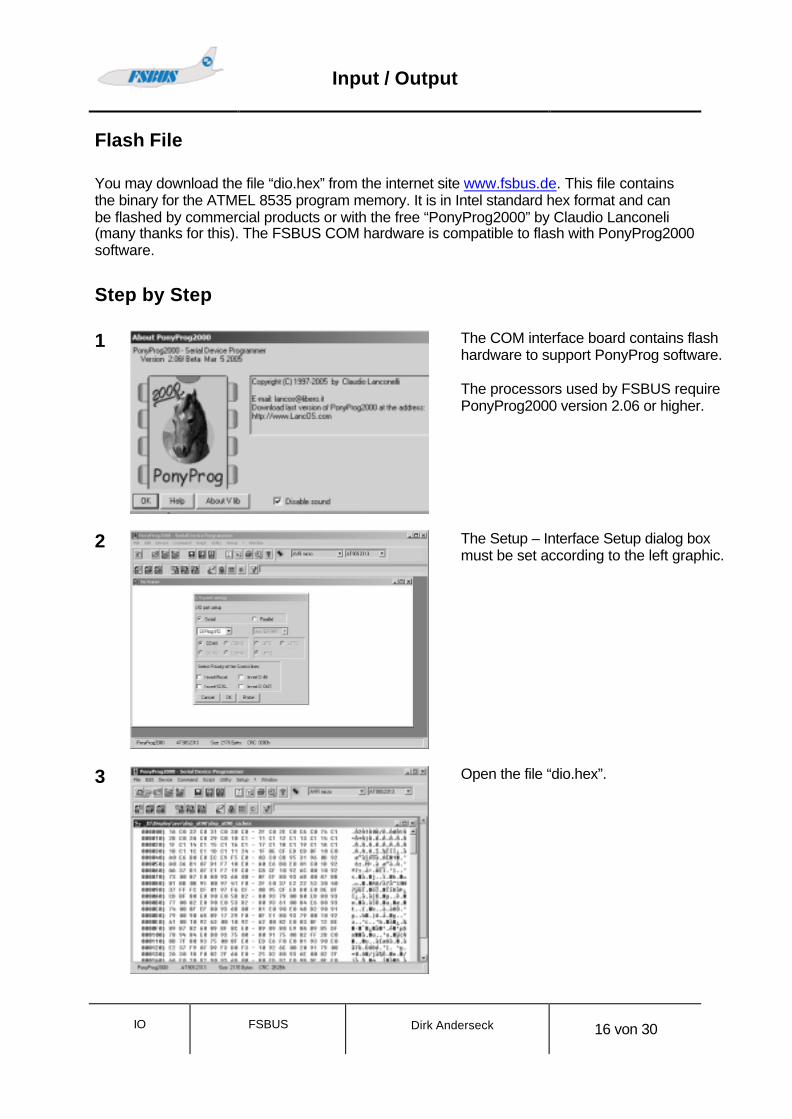
Flash File You may download the file “dio.hex” from the internet site www.fsbus.de. This file contains the binary for the ATMEL 8535 program memory. It is in Intel standard hex format and can be flashed by commercial products or with the free “PonyProg2000” by Claudio Lanconeli (many thanks for this). The FSBUS COM hardware is compatible to flash with PonyProg2000 software.
Step by Step 1
The COM interface board contains flash hardware to support PonyProg software. The processors used by FSBUS require PonyProg2000 version 2.06 or higher.
2
The Setup – Interface Setup dialog box must be set according to the left graphic.
3
Open the file “dio.hex”.

Input / Output
IO
FSBUS
Dirk Anderseck
17 von 30
4
Remove 10-pin FSBUS cable and connect the 6-pin ISP cable from COM board to the IO controller. Take care of correct setting. Pin 1 is marked with the red wire. PonyProg uses the serial COM interface. No other software (FSBUS) should have the serial interface opened!
5
Select the correct processor in PonyProg.
6
Before first flash of the ATMEGA8535, you must setup the security and configuration bits. This is to be done very carefully. Wrong settings may result in a unusable device.
7
You can read the current settings and check it’s correctness.
8
Set the checkboxes according to the left picture and press the “Write” button.

Input / Output
IO
FSBUS
Dirk Anderseck
18 von 30
9
Now it’s time to flash the program into the microcontroller. The Write Program menu point will start it.
10
You will be proud and happy, if the progress window followed by success message appears. Now you can close PonyProg.
11
Remove the 6-pin ISP cable and connect the 10-pin fsbus cable from COM to the new controller.
12
Execute fsadmin.exe which is part of fsbus distribution. Press the com interface button, to open the serial interface. Set the desired controller ID. Select the first panel “Set CID”.
13
Follow the guidelines in textbox. Press the flash button 3 times. With each press, the green LED on IO board should lit for a short period. After this procedure, the new CID is stored in EEPROM.
Input / Output
IO
FSBUS
Dirk Anderseck
19 von 30
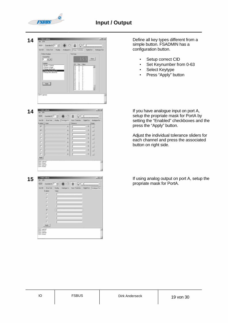
14
Define all key types different from a simple button. FSADMIN has a configuration button.
• Setup correct CID • Set Keynumber from 0-63 • Select Keytype • Press “Apply” button
14
If you have analogue input on port A, setup the propriate mask for PortA by setting the “Enabled” checkboxes and the press the “Apply” button. Adjust the individual tolerance sliders for each channel and press the associated button on right side.
15
If using analog output on port A, setup the propriate mask for PortA.
Input / Output
IO
FSBUS
Dirk Anderseck
20 von 30
Tutorial - Switches
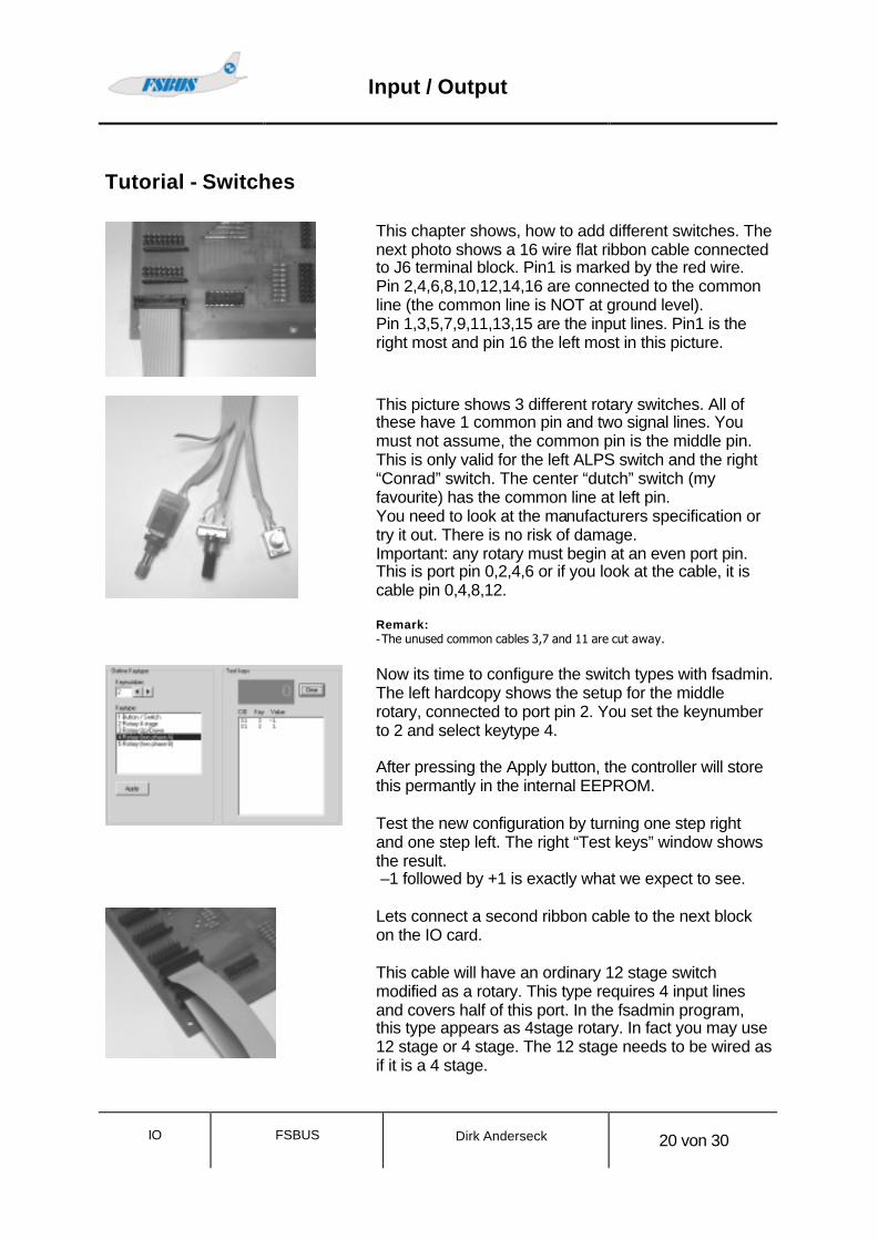
This chapter shows, how to add different switches. The next photo shows a 16 wire flat ribbon cable connected to J6 terminal block. Pin1 is marked by the red wire. Pin 2,4,6,8,10,12,14,16 are connected to the common line (the common line is NOT at ground level). Pin 1,3,5,7,9,11,13,15 are the input lines. Pin1 is the right most and pin 16 the left most in this picture.
This picture shows 3 different rotary switches. All of these have 1 common pin and two signal lines. You must not assume, the common pin is the middle pin. This is only valid for the left ALPS switch and the right “Conrad” switch. The center “dutch” switch (my favourite) has the common line at left pin. You need to look at the manufacturers specification or try it out. There is no risk of damage. Important: any rotary must begin at an even port pin. This is port pin 0,2,4,6 or if you look at the cable, it is cable pin 0,4,8,12. Remark: - The unused common cables 3,7 and 11 are cut away.
Now its time to configure the switch types with fsadmin. The left hardcopy shows the setup for the middle rotary, connected to port pin 2. You set the keynumber to 2 and select keytype 4. After pressing the Apply button, the controller will store this permantly in the internal EEPROM. Test the new configuration by turning one step right and one step left. The right “Test keys” window shows the result. –1 followed by +1 is exactly what we expect to see.
Lets connect a second ribbon cable to the next block on the IO card. This cable will have an ordinary 12 stage switch modified as a rotary. This type requires 4 input lines and covers half of this port. In the fsadmin program, this type appears as 4stage rotary. In fact you may use 12 stage or 4 stage. The 12 stage needs to be wired as if it is a 4 stage.
Input / Output
IO
FSBUS
Dirk Anderseck
21 von 30
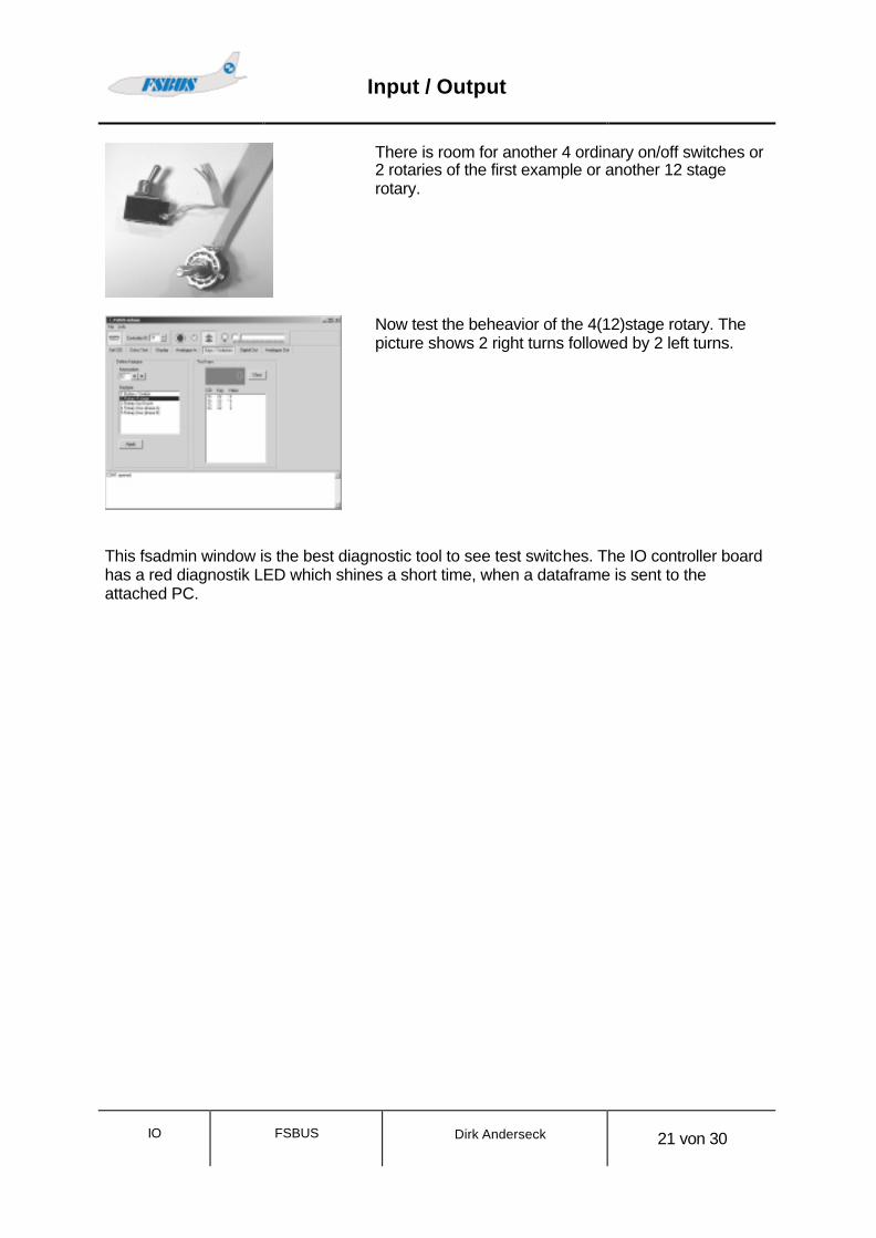
There is room for another 4 ordinary on/off switches or 2 rotaries of the first example or another 12 stage rotary.
Now test the beheavior of the 4(12)stage rotary. The picture shows 2 right turns followed by 2 left turns.
This fsadmin window is the best diagnostic tool to see test switches. The IO controller board has a red diagnostik LED which shines a short time, when a dataframe is sent to the attached PC.
Input / Output
IO
FSBUS
Dirk Anderseck
22 von 30
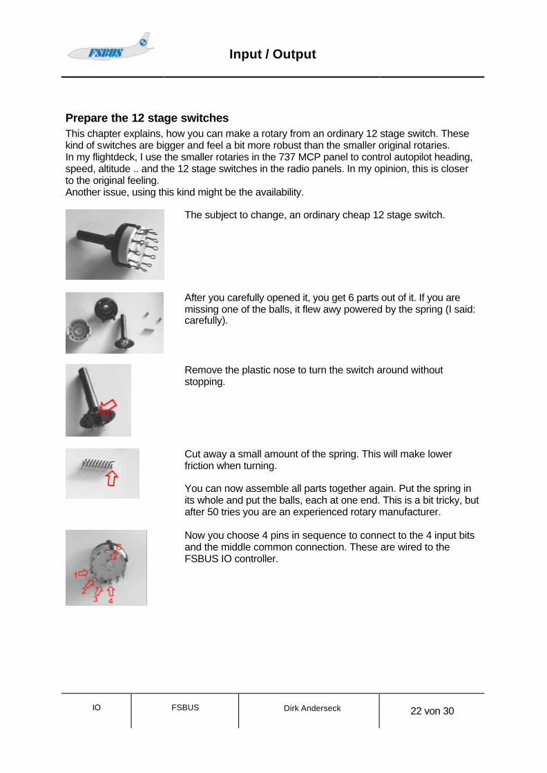
Prepare the 12 stage switches This chapter explains, how you can make a rotary from an ordinary 12 stage switch. These kind of switches are bigger and feel a bit more robust than the smaller original rotaries. In my flightdeck, I use the smaller rotaries in the 737 MCP panel to control autopilot heading, speed, altitude .. and the 12 stage switches in the radio panels. In my opinion, this is closer to the original feeling. Another issue, using this kind might be the availability.
The subject to change, an ordinary cheap 12 stage switch.
After you carefully opened it, you get 6 parts out of it. If you are missing one of the balls, it flew awy powered by the spring (I said: carefully).
Remove the plastic nose to turn the switch around without stopping.
Cut away a small amount of the spring. This will make lower friction when turning. You can now assemble all parts together again. Put the spring in its whole and put the balls, each at one end. This is a bit tricky, but after 50 tries you are an experienced rotary manufacturer.
Now you choose 4 pins in sequence to connect to the 4 input bits and the middle common connection. These are wired to the FSBUS IO controller.
Input / Output
IO
FSBUS
Dirk Anderseck
23 von 30
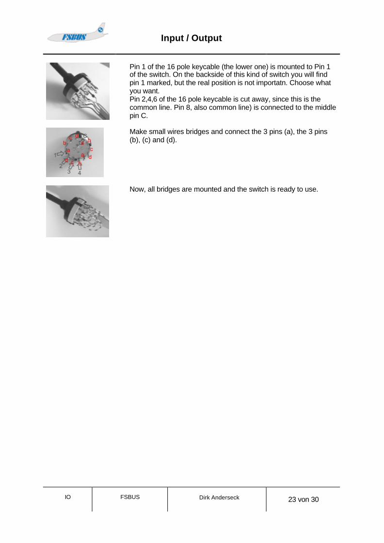
Pin 1 of the 16 pole keycable (the lower one) is mounted to Pin 1 of the switch. On the backside of this kind of switch you will find pin 1 marked, but the real position is not importatn. Choose what you want. Pin 2,4,6 of the 16 pole keycable is cut away, since this is the common line. Pin 8, also common line) is connected to the middle pin C.
Make small wires bridges and connect the 3 pins (a), the 3 pins (b), (c) and (d).
Now, all bridges are mounted and the switch is ready to use.

Input / Output
IO
FSBUS
Dirk Anderseck
24 von 30
Tutorial – AD converter J3 gives the opportunity to connect up to 8 potentiometer. Each value is converted into a binary 8bit value and sent to an attached PC.
A 4k7 linear potentiometer is connected to bit7 of J3. The values of resistors R4-R11 are 1k. IC4 is also mounted to use other ports as output. This affects the linearity a bit but in most cases, this doesn’t matter. C8-C15 are not used in this first example. The 3 pins for each potentiometer are (top to down):
- input - +2.56V - GND
Start fsadmin and set the 7th checkbox to “enabled”. Press “Apply”, the controller will make a reset and after that, you must see the progressbar showing the potentiometer value. That’s all. Remark: If an analogue input is enabled, any attempt to send a digital out signal to that port will fail.
What is the tolerance slider for ? When moving the slider of your potentiometer, you see the red LED burning. That indicates a dataframe sent to PC. Even when slider remains in a position, the LED may continue burning or flickering. This happens, because the resistance of a potentiometer is not as stable as expected. The huge amount of datatraffic is the big disadvantage of this. In most cases there are more than one potentiometers in use and that can drop the FSBUS line performance down. To avoid this, set the tolerance from 0 to 1 or more. Press the right “Apply” button and test again. Soon you will find a position, where the flicker of the red LED stops. You can improve the stability of the AD process also by mounting capacitors(C8-C15) to the ports in use. I suggest a value of 220nF.
Input / Output
IO
FSBUS
Dirk Anderseck
25 von 30
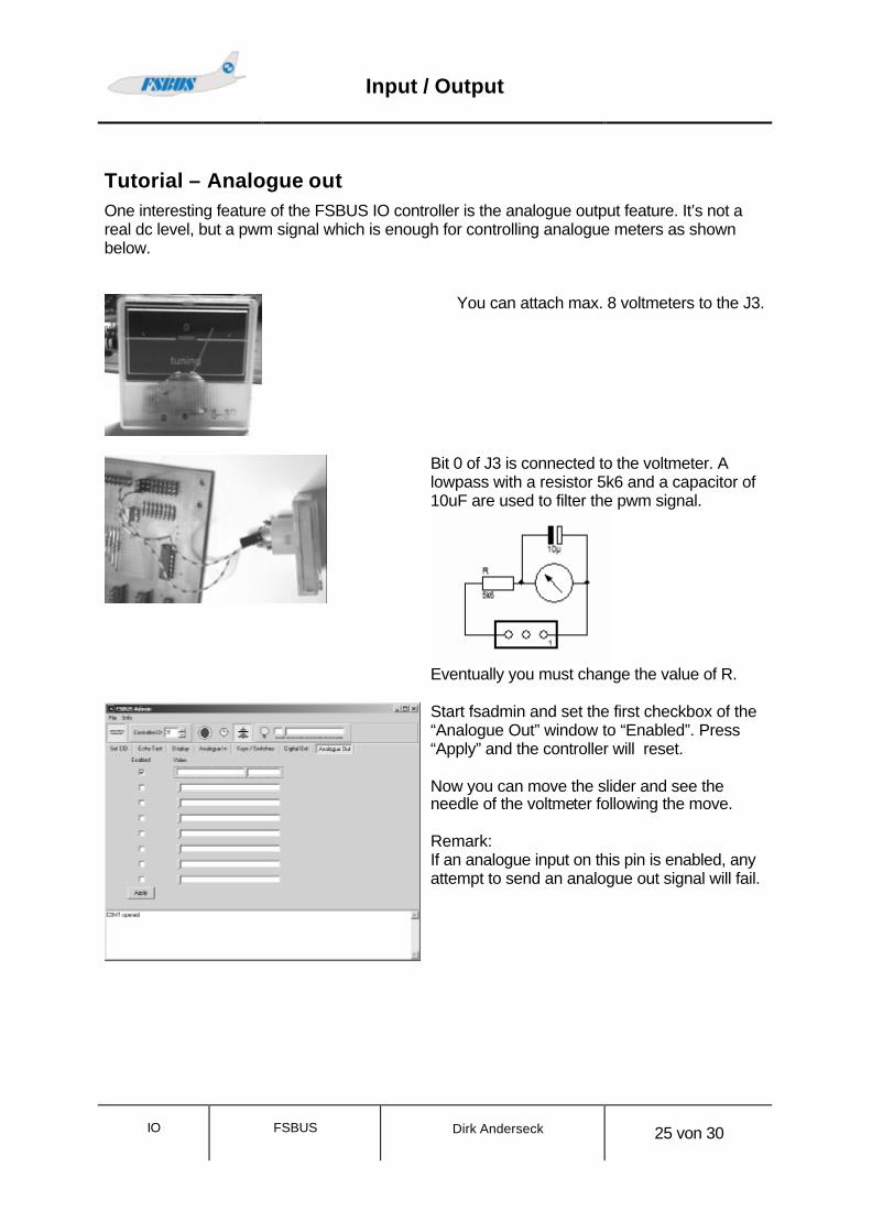
Tutorial – Analogue out One interesting feature of the FSBUS IO controller is the analogue output feature. It’s not a real dc level, but a pwm signal which is enough for controlling analogue meters as shown below.
You can attach max. 8 voltmeters to the J3.
Bit 0 of J3 is connected to the voltmeter. A lowpass with a resistor 5k6 and a capacitor of 10uF are used to filter the pwm signal.
Eventually you must change the value of R.
Start fsadmin and set the first checkbox of the “Analogue Out” window to “Enabled”. Press “Apply” and the controller will reset. Now you can move the slider and see the needle of the voltmeter following the move. Remark: If an analogue input on this pin is enabled, any attempt to send an analogue out signal will fail.

Input / Output
IO
FSBUS
Dirk Anderseck
26 von 30
Tutorial – digital out You can simply mount LED’s and or lamps to J4 and J5. If you don’t use any analogue interface, a total of 16 outputs is possible. IC3 and IC4 are driver chips to decouple the processor from the external environment and to increase the possible current from 20mA to 500mA. Resistors R13-R28 limit the current of each output. This is very important for LED’s. Other devices may not need a resistor. You can insert a wire or a very small resistor (10 Ohm) instead.
This is a small testboard with 8 LED’s mounted on J5. The resistor values R21-R28 are 180 Ohm each.
Again, you can test the LED’s with fsadmin. The LED’s are connected to J5, which is microcontroler port B. If you click on one of the bit cells, it will toggle between 0 and 1. The LED will follow the on/off state.

Input / Output
IO
FSBUS
Dirk Anderseck
27 von 30
Troubleshooting If anything is well done, you can connect the fsbus cable to J2 and the green LED will display the CID. Now some tests to figure out a problem, if this is not the case. The photos are taken with a 30MHz oscilloscope. The black line marks 0V level.
1. Vcc (ATMEGA pin 10) should have 5V stable power supplied from FSBUS COM interface
2. Reset (ATMEGA pin 9) should also have high level near 5V 3. X1 (ATMEGA pin 12) is ~2.5V dc level and a 16MHz sine wave as shown below.
. Hor:0.2us ver:1Vss
4. X2 (ATMEGA pin 13) is ~2V dc level without sine wave. 5. The regular working of firmware can be seen at PD5 (ATMEGA pin 19)
hor:0.5ms ver:1Vss This is the clock for scanning the keyrows (~1.5ms) . Each key is scanned 800 times per second. This is fast enough for the time critical rotaries.
6. If you connect a simple on/off switch to any of the 64 key input lines and close the switch, you may see a 200us negative pulse. The low level must be far below 1V. The high level depends much on the state of other switches in the same row and is not that important. The signal is taken at pin 0 of the key terminal block.
Input / Output
IO
FSBUS
Dirk Anderseck
28 von 30
hor:0.5ms ver:1Vss
7. The transmit signal from IO controller at FSBUS connector pin 10.
hor:1ms ver:1Vss
8. FSBUS connector pin 4 receives data from PC.
hor:0.2ms ver:1Vss
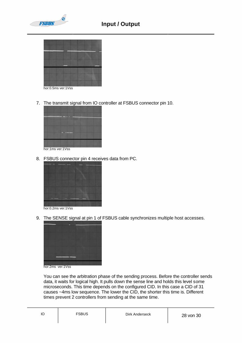
9. The SENSE signal at pin 1 of FSBUS cable synchronizes multiple host accesses.
hor:2ms ver:1Vss
You can see the arbitration phase of the sending process. Before the controller sends data, it waits for logical high. It pulls down the sense line and holds this level some microseconds. This time depends on the configured CID. In this case a CID of 31 causes ~4ms low sequence. The lower the CID, the shorter this time is. Different times prevent 2 controllers from sending at the same time.

Input / Output
IO
FSBUS
Dirk Anderseck
29 von 30
After the low time, the sending controller releases the SENSE line and tests, if no other controller helds it down. Only if SENSE line is high, the transmitting starts. The transmit time is ~1.5ms for 1 FSBUS dataframe. You should keep in mind, that a zero at this line will prevent a FSBUS IO controller from sending anything. If it has a constant low level, something is wrong with cabling or one of the attached controllers.
Information furnished is believed to be accurate and reliable. However, I (Dirk Anderseck) assume no responsibility for the consequences of use of such information nor for any infringement of patents or other rights of third parties which may result from its use. Specification mentioned in this publication are subject to change without notice. This publication supersedes and replaces all information previously supplied. FSBUS Microelectronics are not authorized for use as critical components in life support devices or systems.
Input / Output
IO
FSBUS
Dirk Anderseck
30 von 30
Notes: