diode_ii
TRANSCRIPT

8/8/2019 Diode_II
http://slidepdf.com/reader/full/diodeii 1/24
_______________________________________________________ BASIC
ELECTRONICS
Diode:
When a semiconductor chip contains an N doped region adjacent to a P doped
region, a diode junction (often called a PN junction) is formed. Diode junctions can also be made with either silicon or germanium. However, silicon and germanium are never
mixed when making PN junctions.
A pure silicon crystal or germanium crystal is known as an intrinsic
semiconductor. For most application, there are not enough free electrons and holes in anintrinsic semi-conductor to produce an usable current. The electrical action of these can
be modified by doping means adding impurity atoms to a crystal to increase either the
number of free holes or no of free electrons. When a crystal has been doped, it is called
a extrinsic semi-conductor. They are of two types n-type semiconductor having freeelectrons as majority carriers, p-type semiconductor having free holes as majority
carriers. By themselves, these doped materials are of little use. However, if a junction is
made by joining p-type semiconductor to n-type semiconductor a device is producedwhich is extremely used known as diode. It will allow current to flow through it only in
one direction. The unidirectional properties of a diode allow current flow when forward
biased and disallow current flow when reversed biased. This is called rectification
process and therefore it is called rectifier.
The question now exists how is it possible that by properly joining two semi-
conductors each of which, by itself, will freely conduct the current in any direct refuses
to allow conduction in one direction.
Diodes are useful because electric current will flow through a PN junction in one
direction only. Figure shows the direction in which the current flows.
______________________________________________________________________
_____
SKN Sinhgad College of Engineering, Korti, Pandharpur SKN Sinhgad College of Engineering, Korti, Pandharpur

8/8/2019 Diode_II
http://slidepdf.com/reader/full/diodeii 2/24
_______________________________________________________ BASIC
ELECTRONICS
Consider first the condition of p-type and n-type germanium just prior to joining
fig1 . The majority and minority carriers are in constant motion.
The minority carriers are thermally produced and they exist only for short time
after which they recombine and neutralize each other. In the mean time, other minority
carriers have been produced and this process goes on and on. The number of theseelectron hole pair that exist at any one time depends upon the temperature. The number
of majority carriers is however, fixed depending on the number of impurity atoms
available. While the electrons and holes are in motion but the atoms are fixed in placeand do not move.
______________________________________________________________________
_____
SKN Sinhgad College of Engineering, Korti, Pandharpur SKN Sinhgad College of Engineering, Korti, Pandharpur
8/8/2019 Diode_II
http://slidepdf.com/reader/full/diodeii 3/24
_______________________________________________________ BASIC
ELECTRONICS
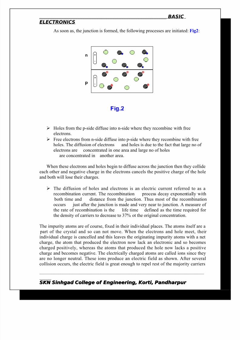
As soon as, the junction is formed, the following processes are initiated: Fig2:
Holes from the p-side diffuse into n-side where they recombine with free
electrons.
Free electrons from n-side diffuse into p-side where they recombine with freeholes. The diffusion of electrons and holes is due to the fact that large no of
electrons are concentrated in one area and large no of holes
are concentrated in another area.
When these electrons and holes begin to diffuse across the junction then they collideeach other and negative charge in the electrons cancels the positive charge of the hole
and both will lose their charges.
The diffusion of holes and electrons is an electric current referred to as arecombination current. The recombination process decay exponentially with
both time and distance from the junction. Thus most of the recombination
occurs just after the junction is made and very near to junction. A measure of the rate of recombination is the life time defined as the time required for
the density of carriers to decrease to 37% ot the original concentration.
The impurity atoms are of course, fixed in their individual places. The atoms itself are a
part of the crystal and so can not move. When the electrons and hole meet, their
individual charge is cancelled and this leaves the originating impurity atoms with a netcharge, the atom that produced the electron now lack an electronic and so becomes
charged positively, whereas the atoms that produced the hole now lacks a positive
charge and becomes negative. The electrically charged atoms are called ions since theyare no longer neutral. These ions produce an electric field as shown. After several
collision occurs, the electric field is great enough to repel rest of the majority carriers
______________________________________________________________________
_____
SKN Sinhgad College of Engineering, Korti, Pandharpur SKN Sinhgad College of Engineering, Korti, Pandharpur

8/8/2019 Diode_II
http://slidepdf.com/reader/full/diodeii 4/24
_______________________________________________________ BASIC
ELECTRONICS
away of the junction. For example, an electron trying to diffuse from n to p side isrepelled by the negative charge of the p-side. Thus diffusion process does not continue
indefinitely but continues as long as the field is developed. The net result of this field is
that it has produced a region, immediately surrounding the junction that has no majoritycarriers. The majority carriers have been repelled away from the junction and junction is
depleted from carriers. The junction is known as the barrier region or depletion regionfig3. The electric field represents a potential difference across the junction also called
space charge potential or barrier potential. This potential is 0.7v for Si at 25 degree
celcious and 0.3v for Ge.
The physical width of the depletion region depends on the doping level. If veryheavy doping is used, the depletion region is physically thin because diffusion charge
need not travel far across the junction before recombination takes place (short life time).
If doping is light, then depletion is more wide (long life time)
Reverse Bias :
When the diode is reverse biased then the depletion region width increases,
majority carriers move away from the junction and there is no flow if current due tomajority carriers but there are thermally produced electron hole pair also. If these
electrons and holes are generated in the vicinity of junction then there is a flow of
current. The negative voltage applied to the diode will tend to attract the holes thus
generated and repel the electrons. At the same time, the positive voltage will attract theelectrons towards the battery and repel the holes. The electron in the p-material and hole
in the n-material are being forced to move forward each other and will probablycombine. This will cause current to flow in entire circuit. This current is usually verysmall (in terms of micro ampher to nano amphere). Since this current is due to minority
carriers and these number of minority carriers are fixed at a given temperature therefore,
the current is almost constant known as reverse saturation current Ico. In actual diode,
______________________________________________________________________
_____
SKN Sinhgad College of Engineering, Korti, Pandharpur SKN Sinhgad College of Engineering, Korti, Pandharpur

8/8/2019 Diode_II
http://slidepdf.com/reader/full/diodeii 5/24
_______________________________________________________ BASIC
ELECTRONICS
the current is not almost constant but increases slightly with voltage. This is due tosurface leakage current. The surface of diode follows ohmic law (V=IR). The resistance
under reverse bias condition is very high 100k to mega ohms. When the reverse voltage
is increased, they and certain value, then breakdown to diode takes place and it conductsheavily. This is due to avalanche or Zener breakdown. Fig4
Forward bias :
When the diode is forward bias, then majority carriers are pushed towards junction, when they collide and recombination takes place. Number of majority carriers
are fixed in semi-conductor. Therefore as each electron is eliminated at the junction, anew electron must be introduced, this comes from battery. At the same time, one holemust be created in p-layer. This is formed by extracting one electron from p-layer.
Therefore, there is a flow of carriers and thus flow of current.
REVIEW:
______________________________________________________________________
_____
SKN Sinhgad College of Engineering, Korti, Pandharpur SKN Sinhgad College of Engineering, Korti, Pandharpur

8/8/2019 Diode_II
http://slidepdf.com/reader/full/diodeii 6/24
_______________________________________________________ BASIC
ELECTRONICS
A diode is an electrical component acting as a one-way valve for current.
When voltage is applied across a diode in such a way that the diode allows
current, the diode is said to be forward-biased.
When voltage is applied across a diode in such a way that the diode prohibits
current, the diode is said to be reverse-biased.
The voltage dropped across a conducting, forward-biased diode is called theforward voltage. Forward voltage for a diode varies only slightly for changes in
forward current and temperature, and is fixed principally by the chemical composition
of the P-N junction.
Silicon diodes have a forward voltage of approximately 0.7 volts.
Germanium diodes have a forward voltage of approximately 0.3 volts.
The maximum reverse-bias voltage that a diode can withstand without "breakingdown" is called the Peak Inverse Voltage, or PIV rating.
______________________________________________________________________
_____
SKN Sinhgad College of Engineering, Korti, Pandharpur SKN Sinhgad College of Engineering, Korti, Pandharpur

8/8/2019 Diode_II
http://slidepdf.com/reader/full/diodeii 7/24
_______________________________________________________ BASIC
ELECTRONICS
METER CHECK OF DOODE
______________________________________________________________________
_____
SKN Sinhgad College of Engineering, Korti, Pandharpur SKN Sinhgad College of Engineering, Korti, Pandharpur

8/8/2019 Diode_II
http://slidepdf.com/reader/full/diodeii 8/24
_______________________________________________________ BASIC
ELECTRONICS
Space Charge Capacitance on Transition Capacitive C T :
Reverse bias causes majority carriers to move away from the junction, thereby
creating more ions. Hence the thickness of depletion region increases. This region behaves as the dielectric material used for making capacitors. The p-type and n-typeconducting on each side of dielectric act as the plate. The incremental capacitance CT is
defined by
Where, dQ is the increase in charge caused by a change dv in voltage.
CT is not constant, it depends upon applied voltage, therefore it is defined asdQ/dV. When p-n junction is forward biased, then also a capacitance is defined called
diffusion capacitance CD (rate of change of injected charge with voltage) to take intoaccount the time delay in moving the charges across the junction by the diffusion process. Therefore, it cannot be identified in terms of a dielectric and plates as space
charge capacitance. It must be considered as a fictitious element that allow us to predict
time delay. If the amount of charge to be moved across the junction is increased, thetime delay is greater, it follows that diffusion capacitance varies directly with the
magnitude of forward current.
Real Diode: Small Signal Operation: (Load Line)
Consider the diode circuit shown in Fig.5
______________________________________________________________________
_____
SKN Sinhgad College of Engineering, Korti, Pandharpur SKN Sinhgad College of Engineering, Korti, Pandharpur

8/8/2019 Diode_II
http://slidepdf.com/reader/full/diodeii 9/24
_______________________________________________________ BASIC
ELECTRONICS
This equation involves two unknown and can not be solved. The other equation
in terms of these two variables is given by the static characteristic. The straight line
represented by this above equation is known as the load line. The load line pass through
two points, I = 0, VD = V and VD = 0, I = V / RL . The slope of this line is equal to 1/RL. The point of inter–section of straight line and diode characteristic gives the
operating point. Fig.6
Say V=1V, RL=10ohm. (Fig7).
______________________________________________________________________
_____
SKN Sinhgad College of Engineering, Korti, Pandharpur SKN Sinhgad College of Engineering, Korti, Pandharpur

8/8/2019 Diode_II
http://slidepdf.com/reader/full/diodeii 10/24
_______________________________________________________ BASIC
ELECTRONICS
Therefore, as the diode voltage varies, diode current also varies, sinusoidally (Fig 8).
______________________________________________________________________
_____
SKN Sinhgad College of Engineering, Korti, Pandharpur SKN Sinhgad College of Engineering, Korti, Pandharpur

8/8/2019 Diode_II
http://slidepdf.com/reader/full/diodeii 11/24
_______________________________________________________ BASIC
ELECTRONICS
In certain applications only a.c. equivalent circuit is required. Since only a.c.response of the circuit is considered D.C. Source is not shown (Fig 9). The resistance rf
represents the dynamic resistance or a.c. resistance of the diode .It is obtained by taking
the ratio of at operating point.
Fig. 9
Dynamic Resistance,
Diode Approximation: (Large signal operations):
1. Ideal Diode :
When forward biased, resistance offered is zero, When reverse biased resistance
offered is infinity. It acts as a perfect switch.Fig10
______________________________________________________________________
_____
SKN Sinhgad College of Engineering, Korti, Pandharpur SKN Sinhgad College of Engineering, Korti, Pandharpur

8/8/2019 Diode_II
http://slidepdf.com/reader/full/diodeii 12/24
_______________________________________________________ BASIC
ELECTRONICS
2. Second Approximation: when forward voltage is more than 0.7 V, for Si then itconducts and offers zero resistance. Fig 11.
3. 3rd Approximation:
When forward voltage is more than 0.7 v, then it conduct and offer bulk resistance
Rf (slope of the current) fig.12
______________________________________________________________________
_____
SKN Sinhgad College of Engineering, Korti, Pandharpur SKN Sinhgad College of Engineering, Korti, Pandharpur

8/8/2019 Diode_II
http://slidepdf.com/reader/full/diodeii 13/24
_______________________________________________________ BASIC
ELECTRONICS
When reverse biased resistance offered is very high. (and not infinity). Then the
diode equivalent circuit is as shown in fig13.
Problem:
Calculate the voltage output for following inputs
(a) V1=V2=0.
(b) V1=V, V2=0.
. (c) V=V2=V knew voltage =Vr
Forward resistance is Rf.
______________________________________________________________________
_____
SKN Sinhgad College of Engineering, Korti, Pandharpur SKN Sinhgad College of Engineering, Korti, Pandharpur

8/8/2019 Diode_II
http://slidepdf.com/reader/full/diodeii 14/24
_______________________________________________________ BASIC
ELECTRONICS
Solution:
(a). Vo = 0.
(b). V1 = V, V2 = V.
(c) V1 = V 2 = V.
______________________________________________________________________
_____
SKN Sinhgad College of Engineering, Korti, Pandharpur SKN Sinhgad College of Engineering, Korti, Pandharpur

8/8/2019 Diode_II
http://slidepdf.com/reader/full/diodeii 15/24
_______________________________________________________ BASIC
ELECTRONICS
Applications
Half wave Rectifier (fig.17)
______________________________________________________________________
_____
SKN Sinhgad College of Engineering, Korti, Pandharpur SKN Sinhgad College of Engineering, Korti, Pandharpur

8/8/2019 Diode_II
http://slidepdf.com/reader/full/diodeii 16/24
_______________________________________________________ BASIC
ELECTRONICS
Fig.17
In positive half cycle, D is forward biased (ideal) and output voltage is same the
input voltage. In the negative half cycle, D is reverse biased, and output voltage is zero.
When the diode is reverse biased, entire transformer voltage appears across the
diode. The maximum voltage across the diode is Vm. The diode must be capable to
withstand this voltage. Therefore PIV rating of diode should be equal to Vm in half
wave rectifiers. The avg-current rating must case of single phase be greater than Iavg.
Full Wave Rectifier: (fig.18)
______________________________________________________________________
_____
SKN Sinhgad College of Engineering, Korti, Pandharpur SKN Sinhgad College of Engineering, Korti, Pandharpur

8/8/2019 Diode_II
http://slidepdf.com/reader/full/diodeii 17/24
_______________________________________________________ BASIC
ELECTRONICS
Fig18
Fig18graph
Center tap transformer. It is more efficient and supplies current in both half cycles.
• In the first half cycle D1is forward biased and conducts. D2 is reverse biased.• In the second half cycle D2 is forward biased, and conducts.
______________________________________________________________________
_____
SKN Sinhgad College of Engineering, Korti, Pandharpur SKN Sinhgad College of Engineering, Korti, Pandharpur

8/8/2019 Diode_II
http://slidepdf.com/reader/full/diodeii 18/24
_______________________________________________________ BASIC
ELECTRONICS
When D1 conducts, then full secondary voltage appears across D2, therefore PIV rating
of the diode should be 2 Vm.
Bridge Rectifier: Fig 19
Figure: 19
Most widely used rectifier. In the positive half cycle, D1and D4 are forward
biased and D2and D3 are reverse biased. In the negative half cycle,D1and D3 areforward biased .The output voltage waveform is same but the advantage is that PIV
rating of diodes are Vm and only single secondary transformer for Vm voltage is
required. The main disadvantage is that it requires four diodes. When now d. c. voltageis required then secondary voltage is low and diode drop (1.4V) becomes significant.
The Xfr, required is of high rating (>1.4 V). For low D.C. output we use centre tap
rectifier because only one diode drop is there. The ripple factor is the measure of the purity of D.C. output of a rectifier and is defined as
______________________________________________________________________
_____
SKN Sinhgad College of Engineering, Korti, Pandharpur SKN Sinhgad College of Engineering, Korti, Pandharpur

8/8/2019 Diode_II
http://slidepdf.com/reader/full/diodeii 19/24
_______________________________________________________ BASIC
ELECTRONICS
Zener Diode :
The diodes designed to work in breakdown region are called zener diode. The
power handling capacity of these diodes is better. The power dissipation of a zener diode equals the product of its voltage and current. PZ =VZ IZ. When zener is forward
biased it works as a diode and drop across it is 0.7V when it works in breakdown region
the voltage across it is constant Vz and the current through it is decided by externalresistance. Zener diode is used for regulating the dc voltage. It maintains the output
voltage constant even through the current through changes.
______________________________________________________________________
_____
SKN Sinhgad College of Engineering, Korti, Pandharpur SKN Sinhgad College of Engineering, Korti, Pandharpur

8/8/2019 Diode_II
http://slidepdf.com/reader/full/diodeii 20/24
_______________________________________________________ BASIC
ELECTRONICS
Fig. 35
To operate the zener in Breakdown region Vs should always be greater then Vz.
Rs is used to limit the current. If the Vs voltage changes operating point also changessimultaneously but voltage across zener is almost constant. Fig. 37 The firstapproximation zener diode is a voltage source of Vz magnitude and second
approximation includes the resistance also.
______________________________________________________________________
_____
SKN Sinhgad College of Engineering, Korti, Pandharpur SKN Sinhgad College of Engineering, Korti, Pandharpur

8/8/2019 Diode_II
http://slidepdf.com/reader/full/diodeii 21/24
_______________________________________________________ BASIC
ELECTRONICS
______________________________________________________________________
_____
SKN Sinhgad College of Engineering, Korti, Pandharpur SKN Sinhgad College of Engineering, Korti, Pandharpur

8/8/2019 Diode_II
http://slidepdf.com/reader/full/diodeii 22/24
_______________________________________________________ BASIC
ELECTRONICS
(Fig.38) The resistance produces more I*R drop as the current increases.
The voltage at Q1 is ,
V1 = Rz +Vz
At Q2 = I2 +R2 +Vz
Change in voltage is,
If zener is used to regulate the voltage across a load resistance. The zener is willwork in the breakdown region only if the thevenin voltage across zener is more than V
Z
If zener is operating in breakdown region, the series current will be given by,
______________________________________________________________________
_____
SKN Sinhgad College of Engineering, Korti, Pandharpur SKN Sinhgad College of Engineering, Korti, Pandharpur

8/8/2019 Diode_II
http://slidepdf.com/reader/full/diodeii 23/24
_______________________________________________________ BASIC
ELECTRONICS
Zener Drop Output point:
For a zener regulator to hold the output voltage constant, zener diode must
remain in the breakdown region under all operating conditions, i.e. there must be zener
current for all source voltage load currents. The worst case occurs for minimum sourcevoltage and maximum load current.
The critical point occurs when maximum load current equals minimum seriescurrent
When the zener diode operates in breakdown region, the voltage Vz across itremains fairly constant even though the current Iz through it vary considerably. If the
load IL should increase, the current Iz should decrease by the same percentage in order to maintain load current constant Is. This keeps the voltage drop across Rs constant andhence the output voltage. If the input voltage should increase, the zener diode passes a
larger current, that extra voltage is dropped across the resistance Rs. If input voltage
falls, the current Iz falls such that Vz is constant.
______________________________________________________________________
_____
SKN Sinhgad College of Engineering, Korti, Pandharpur SKN Sinhgad College of Engineering, Korti, Pandharpur

8/8/2019 Diode_II
http://slidepdf.com/reader/full/diodeii 24/24
_______________________________________________________ BASIC
ELECTRONICS
______________________________________________________________________
_____
SKN Sinhgad College of Engineering, Korti, Pandharpur SKN Sinhgad College of Engineering, Korti, Pandharpur