digital sigma-delta modulator with hi snr...
TRANSCRIPT
FACULDADE DE ENGENHARIA DA UNIVERSIDADE DO PORTO
Digital Sigma-Delta modulator with HiSNR (100dB+)
Ricardo Jorge Moreira Pereira
PROVISIONAL VERSION
Master in Electrical and Computer Engineering
Supervisor: José Carlos dos Santos Alves (PhD)
Co-supervisor: Pedro Faria de Oliveira (Eng)
June, 2011

c© Copyright by Ricardo Pereira, 2011
Some rights reserved
You are free:
to Share — to copy, distribute and transmit the work.
Under the following conditions:
Attribution — You must attribute the work in the manner specified by the author
or licensor (but not in any way that suggests that they endorse you or your use
of the work).
Noncommercial — You may not use this work for commercial purposes.
No Derivative Works — You may not alter, transform, or build upon this work.
With the understanding that:
Waiver — Any of the above conditions can be waived if you get permission from the copy-
right holder.
Other Rights — In no way are any of the following rights affected by the license:
• Your fair dealing or fair use rights;
• The author’s moral rights;
• Rights other persons may have either in the work itself or in how the work is used, such as
publicity or privacy rights.
Notice — For any reuse or distribution, you must make clear to others the license terms of this
work. Please display this page for that purpose.

Resumo
Desde o aparecimento de blocos de processamento digital que a conversão de analógico paradigital e de digital para analógico se revelou bastante importante. A grande maioria do proces-samento hoje em dia é feito num nível digital, o que permite velocidades de processamento maiselevadas. Outras vantagens são a fácil descomposição de elementos digitais em outros mais sim-ples de forma a melhor estruturar e aumentar ainda mais as capacidades de um determinado bloco.Os blocos digitais possuem inerentemente menor consumo que os correspondentes analógicos epermitem facilmente implementar ou acrescentar novas unidades de processamento digitais, igual-mente integradas e de baixo consumo.
Apesar de o processamento ser feito digitalmente, o mundo, mantém-se um lugar analógico,assim como nós mesmos. Isso apresenta o problema de recolher os dados analógicos, transforma-los para um formato digital, e após o processamento devido, torna-los novamente analógicos paraserem percebidos e absorvidos por nós, se caso for. É nesta lógica de transformação que existemos conversores Analógico para Digital (ADC), e Digital para Analógico (DAC). Além desses prob-lemas, com os avanços na construção de circuitos em digitais que se assistiu nas ultimas décadas,a velocidade de processamento aumentou ainda mais. Isto origina que os conversores são muitasvezes limitadores de desempenho dos processadores, na medida em que só se podem processardados que já existam e tenham sido recolhidos para o núcleo.
Para combater o problema da velocidade, e também para aumentar a resolução dos dados aserem processados, recorre-se inúmeras vezes a conversores sobre amostrados. Isto são conver-sores em que uma determinada amostra analógica faz correspondencia com variadas amostrasdigitais e vice-versa. Isto aumenta a velocidade de entrada e de saída dos dados do circuito to-tal. Utilizando sobre amostragem um bloco de processamento não tem de esperar que uma novaamostra fique pronta para começar a processar, e da mesma forma um dado de saída do bloco podesignificar variados dados de saída do circuito.
Uma das formas mais eficazes, apesar de muitas vezes descorada, de utilizar conversores sobreamostrados é a aplicação de conversores Sigma Delta (Σ∆). Estes conversores fazem uso dos con-ceitos de Quantização, Sobre Amostragem e de Noise Shaping, por forma a garantir um acréscimode dados, e de não permitir que os erros associados a cada recolha não se torne um factor muitoimportante no decréscimo do desempenho do núcleo.
Esta dissertação tem como tema a aplicação digital de um Σ∆, em especial na componentede conversão de recolha digital e sobre amostragem da parte digital antes de ser convertida paraanalógico. Os desafios encontram-se ao nível de aumentar o desempenho, assim como de mini-mizar parâmetros de implementação, como a área de circuito a utilizar e o consumo de potência.O objectivo final desta dissertação é de criar um conversor Σ∆ para aplicações em áudio.
i

ii
Abstract
Since the onset of processing cores that the conversion from digital to analog and analog todigital has proved very important. The vast majority of the processing today is done on a digitallevel, which allows higher processing speeds. Other advantages are the easy decomposition ofdigital elements into simpler ones in order to better structure and further enhance the capabilitiesof a particular core. The digital core are capable of less power conssumption compared with theanalogue counterparts, and more importantly, they permit the implemenation or agregation of newprocessing cores, equally integrated and with low power demands.
Although the processing is done digitally, the world remains an analog place, as well as our-selves. This presents the problem of collecting analog data, transforms them into a digital format,and after the due process, transform it back to analog to be perceived and absorbed by us, if ap-plied. It is this transformation logic that there are Analog to Digital Converters (ADC) and Digitalto Analog Converters (DAC). Besides these problems, with advances in the construction of digitalcircuits seen over the last decades, the processing speed increased even further. This causes thatthe converters are often a limiting factor for the processors, in that it can only process data thatalready exist and was driven into the core.
To combat the problem of speed, and also to increase the resolution of the data to the proces-sor, many times is used what is called of over sampled converters. In this converter a given analogsample has correspondence with various digital samples and vice versa. This increases the speedof the input and output data for the total circuit. Now a processing block does not have to wait for agiven sample to be ready to begin processing, and likewise a core output data can mean numerousoutputs of the circuit.
One of the most effective, although often discarded, oversample converter is the Delta Sigmaconverters (Σ∆). These converters make use of the concepts of Quantization, Over Sampling andNoise Shaping in order to ensure greater data sampling, and to remove as far as possible, the errorsassociated with each collection, and thus not become a very important factor in decreasing the coreperformance.
This dissertation has in its theme the digital application of a Σ∆, especially in the digitalsampling of the digital data before being converted to analog. The challenges are to increase thelevel of performance as well as to minimize implementation parameters, such as the use of circuitarea and power consumption. The ultimate goal of this dissertation is to create a converter Σ∆ foraudio performance with pre-defined performance guidelines.
iii

iv

Agradecimentos
Gostaria antes de tudo agradecer ao Professor Doutor José Carlos Alves e ao Engenheiro Pe-dro Faria de Oliveira pela oportunidade que me foi dada em realizar esta dissertação, por tudo oque aprendi e por todo o apoio prestado na duração da mesma.
Agradeço a todos os elementos da sala I221, pelos momentos de camaradagem. Queria tam-bém agradecer aos Engenheiros Eduardo Sousa, Ricardo Sousa e também ao Miguel Caetano, e atodos os que de uma forma ou de outra me acompanharam, e me ajudaram a chegar a bom portoneste desafio, tanto amigos, como professores e colegas.
E finalmente não queria deixar de referir o aspecto mais importante de todos, a minha famíliaque apesar de muitas dificuldades me permitiu chegar a este momento, e sem duvida são o pilarde tudo o que alcancei até então, e por tudo o que a vida ainda me trouxer.
Um sincero muito obrigado a todos os acima referidos.
Ricardo Jorge Moreira Pereira
v

vi

"Now here, you see,it takes all the running you can do, to keep in the same place.
If you want to get somewhere else, you must run at least twice as fast as that!"
Red Queen in Through the Looking-Glass, Lewis Carroll
vii

viii
Contents
1 Introduction 11.1 Motivation . . . . . . . . . . . . . . . . . . . . . . . . . . . . . . . . . . . . . . 11.2 Objectives . . . . . . . . . . . . . . . . . . . . . . . . . . . . . . . . . . . . . . 11.3 Thesis Presentation . . . . . . . . . . . . . . . . . . . . . . . . . . . . . . . . . 21.4 Thesis Structure . . . . . . . . . . . . . . . . . . . . . . . . . . . . . . . . . . . 3
2 State of the Art 52.1 Brief History . . . . . . . . . . . . . . . . . . . . . . . . . . . . . . . . . . . . 52.2 Sigma-Delta Naming . . . . . . . . . . . . . . . . . . . . . . . . . . . . . . . . 6
2.2.1 Internal Workings . . . . . . . . . . . . . . . . . . . . . . . . . . . . . . 62.3 The necessity in Oversampling and Conversion . . . . . . . . . . . . . . . . . . 72.4 Sigma-Delta Modulation . . . . . . . . . . . . . . . . . . . . . . . . . . . . . . 8
2.4.1 Oversampling . . . . . . . . . . . . . . . . . . . . . . . . . . . . . . . . 82.4.2 Quantization Error . . . . . . . . . . . . . . . . . . . . . . . . . . . . . 92.4.3 Noise Shaping . . . . . . . . . . . . . . . . . . . . . . . . . . . . . . . 112.4.4 Σ∆ Performance . . . . . . . . . . . . . . . . . . . . . . . . . . . . . . 11
2.5 Sigma-Delta Architecture . . . . . . . . . . . . . . . . . . . . . . . . . . . . . . 132.6 Circuit Architecture . . . . . . . . . . . . . . . . . . . . . . . . . . . . . . . . . 14
2.6.1 Stability . . . . . . . . . . . . . . . . . . . . . . . . . . . . . . . . . . . 152.7 Circuit Design . . . . . . . . . . . . . . . . . . . . . . . . . . . . . . . . . . . . 15
2.7.1 Power Consumption . . . . . . . . . . . . . . . . . . . . . . . . . . . . 152.8 Conclusions . . . . . . . . . . . . . . . . . . . . . . . . . . . . . . . . . . . . . 16
3 Σ∆ Modulation 173.1 Theoretical Study . . . . . . . . . . . . . . . . . . . . . . . . . . . . . . . . . . 17
3.1.1 ENOB . . . . . . . . . . . . . . . . . . . . . . . . . . . . . . . . . . . . 173.1.2 Modulator Architectures . . . . . . . . . . . . . . . . . . . . . . . . . . 183.1.3 Techniques to increase the SNR . . . . . . . . . . . . . . . . . . . . . . 193.1.4 Noise Power Level . . . . . . . . . . . . . . . . . . . . . . . . . . . . . 20
3.2 Signal Modulation . . . . . . . . . . . . . . . . . . . . . . . . . . . . . . . . . 213.2.1 Wave Modulation . . . . . . . . . . . . . . . . . . . . . . . . . . . . . . 223.2.2 Wave modulation in the data path . . . . . . . . . . . . . . . . . . . . . 23
3.3 Interpolation Filter . . . . . . . . . . . . . . . . . . . . . . . . . . . . . . . . . 253.3.1 The need for interpolation . . . . . . . . . . . . . . . . . . . . . . . . . 253.3.2 Interpolation Filter for Σ∆ DAC . . . . . . . . . . . . . . . . . . . . . . 253.3.3 FIR versus IIR Filters . . . . . . . . . . . . . . . . . . . . . . . . . . . . 253.3.4 Designing a cascade Interpolation Filter . . . . . . . . . . . . . . . . . . 27
3.4 Conclusions . . . . . . . . . . . . . . . . . . . . . . . . . . . . . . . . . . . . . 35
ix

x CONTENTS
4 Digital Σ∆ Modulator 374.1 MATLAB Simulation . . . . . . . . . . . . . . . . . . . . . . . . . . . . . . . . 37
4.1.1 Simulated Modulator . . . . . . . . . . . . . . . . . . . . . . . . . . . . 374.1.2 SNR in the Input . . . . . . . . . . . . . . . . . . . . . . . . . . . . . . 384.1.3 Dynamic Parameters . . . . . . . . . . . . . . . . . . . . . . . . . . . . 394.1.4 Demodulation . . . . . . . . . . . . . . . . . . . . . . . . . . . . . . . . 414.1.5 SNR in the Output . . . . . . . . . . . . . . . . . . . . . . . . . . . . . 45
4.2 HDL Implementation . . . . . . . . . . . . . . . . . . . . . . . . . . . . . . . . 454.2.1 Proposed Σ∆ Modulator . . . . . . . . . . . . . . . . . . . . . . . . . . 454.2.2 Verification Process . . . . . . . . . . . . . . . . . . . . . . . . . . . . . 474.2.3 Data Path . . . . . . . . . . . . . . . . . . . . . . . . . . . . . . . . . . 484.2.4 Wave Reconstruction . . . . . . . . . . . . . . . . . . . . . . . . . . . . 504.2.5 SNR in the Input . . . . . . . . . . . . . . . . . . . . . . . . . . . . . . 514.2.6 SNR in the Output . . . . . . . . . . . . . . . . . . . . . . . . . . . . . 51
5 Conclusions 535.1 Conclusions . . . . . . . . . . . . . . . . . . . . . . . . . . . . . . . . . . . . . 53
5.1.1 Incomplete Work . . . . . . . . . . . . . . . . . . . . . . . . . . . . . . 545.2 Future Work . . . . . . . . . . . . . . . . . . . . . . . . . . . . . . . . . . . . . 555.3 Final Considerations . . . . . . . . . . . . . . . . . . . . . . . . . . . . . . . . 56
References 57

List of Figures
2.1 Digital Sigma Delta block diagram . . . . . . . . . . . . . . . . . . . . . . . . . 62.2 Internal Workings for the First Order Sigma Delta . . . . . . . . . . . . . . . . . 72.3 Simple representation of a DSP core and IO ports [1] . . . . . . . . . . . . . . . 82.4 a) Nyquist rate b) oversample rate[2] . . . . . . . . . . . . . . . . . . . . . . . . 92.5 Quantization error with N=3 [3] . . . . . . . . . . . . . . . . . . . . . . . . . . 102.6 Quantization process. a)Step size. b) Quantization error. c) Probability density of
white quantization noise. d) Linear model. [2] . . . . . . . . . . . . . . . . . . . 102.7 One bitstream, First order Σ∆ Modulator [4] . . . . . . . . . . . . . . . . . . . . 142.8 One bit, Digital to Digital Converter [4] . . . . . . . . . . . . . . . . . . . . . . 142.9 One bitstream, Second order Σ∆ Modulator . . . . . . . . . . . . . . . . . . . . 15
3.1 Building blocks for a full DAC architecture [5] . . . . . . . . . . . . . . . . . . 223.2 Input wave and resulting Bitstream for an OSR = 1 . . . . . . . . . . . . . . . . 223.3 Input wave and resulting Bitstream for an OSR = 2 . . . . . . . . . . . . . . . . 233.4 Input wave and resulting Bitstream for an OSR = 4 . . . . . . . . . . . . . . . . 233.5 A)Input B)Error C)Accumulator D)Output . . . . . . . . . . . . . . . . . . . . . 243.6 A)Input B)Error C)Accumulator D)Output . . . . . . . . . . . . . . . . . . . . . 243.7 Magnitude and Phase response for a FIR Equiripple filter . . . . . . . . . . . . . 263.8 Magnitude and Phase responce for a IIR Elliptical filter . . . . . . . . . . . . . . 273.9 Cascaded Interpolation Filter [6] . . . . . . . . . . . . . . . . . . . . . . . . . . 283.10 Spectrum of the Input on the Interpolation filter . . . . . . . . . . . . . . . . . . 283.11 Spectrum of the output of the first stage . . . . . . . . . . . . . . . . . . . . . . 303.12 Magnitude and Phase response for the second stage Equiripple filter . . . . . . . 313.13 Spectrum of the output of the second stage . . . . . . . . . . . . . . . . . . . . . 313.14 Magnitude and Phase response for the third stage Equiripple filter . . . . . . . . 323.15 Spectrum of the output of the third stage . . . . . . . . . . . . . . . . . . . . . . 333.16 Magnitude and Phase response for the 16 times interpolation S/H . . . . . . . . . 343.17 Output spectrum of the Cascaded Interpolation Filter . . . . . . . . . . . . . . . 34
4.1 Second Order Implementation . . . . . . . . . . . . . . . . . . . . . . . . . . . 384.2 SNR and ENOB . . . . . . . . . . . . . . . . . . . . . . . . . . . . . . . . . . . 394.3 a) RMS signal b) RMS noise . . . . . . . . . . . . . . . . . . . . . . . . . . . . 394.4 Second Order Modulator . . . . . . . . . . . . . . . . . . . . . . . . . . . . . . 404.5 A) Data in B) Error2 . . . . . . . . . . . . . . . . . . . . . . . . . . . . . . . . 414.6 C) Acc2 D) Bitstream . . . . . . . . . . . . . . . . . . . . . . . . . . . . . . . . 424.7 A) Data in B) Error2 . . . . . . . . . . . . . . . . . . . . . . . . . . . . . . . . 434.8 C) Acc2 D) Bitstream . . . . . . . . . . . . . . . . . . . . . . . . . . . . . . . . 434.9 Digital Input Wave . . . . . . . . . . . . . . . . . . . . . . . . . . . . . . . . . 44
xi

xii LIST OF FIGURES
4.10 Analogue Output Wave . . . . . . . . . . . . . . . . . . . . . . . . . . . . . . . 444.11 Spectrum for the MATLAB simulation . . . . . . . . . . . . . . . . . . . . . . . 464.12 Block Diagram for the Code . . . . . . . . . . . . . . . . . . . . . . . . . . . . 464.13 Verification Process . . . . . . . . . . . . . . . . . . . . . . . . . . . . . . . . . 474.14 Generated Sine Wave . . . . . . . . . . . . . . . . . . . . . . . . . . . . . . . . 494.15 A)Input B)Error1 C)Acc1 D)Error2 E)bitstream . . . . . . . . . . . . . . . . . 494.16 Reconstructed Sine Wave . . . . . . . . . . . . . . . . . . . . . . . . . . . . . . 504.17 Spectrum for the Output wave . . . . . . . . . . . . . . . . . . . . . . . . . . . 52

List of Tables
2.1 Σ∆ Power Comparison for Different Technologies . . . . . . . . . . . . . . . . . 16
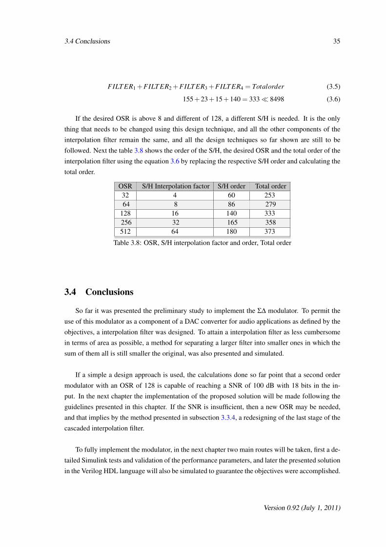
3.1 SNR in dB according to L and OSR [4] . . . . . . . . . . . . . . . . . . . . . . 183.2 Noise Power of 18 bits quantization by Technology I-O input levels . . . . . . . 213.3 Filter Order in Single Stage for FIR and IIR . . . . . . . . . . . . . . . . . . . . 263.4 First Stage Filter Characteristics . . . . . . . . . . . . . . . . . . . . . . . . . . 293.5 Second Stage Filter Characteristics . . . . . . . . . . . . . . . . . . . . . . . . . 303.6 Third Stage Filter Characteristics . . . . . . . . . . . . . . . . . . . . . . . . . . 323.7 Sample and Hold Filter Characteristics . . . . . . . . . . . . . . . . . . . . . . . 333.8 OSR, S/H interpolation factor and order, Total order . . . . . . . . . . . . . . . . 35
4.1 MATLAB function for demodulation . . . . . . . . . . . . . . . . . . . . . . . . 424.2 Input Wave Characteristics . . . . . . . . . . . . . . . . . . . . . . . . . . . . . 49
xiii

xiv LIST OF TABLES

Abbreviations and Symbols
σ2(e) Total Noise Power
∆ DeltaΣ SigmaΣ∆ Sigma DeltaAAF Anti Aliasing FilterADC Analoge-to-digital convertersAMS Austria Micro SystemsCAD Computer Aided DesignCAE Computer Aided EngineeringCMOS Complementary Metal–Oxide–SemiconductorDDC Digital to Digital ConverterDSP Digital Signal ProcessorDUT Device Under TestEDA Electronic design automationFEUP Faculdade de Engenharia da Universidade do PortoFIR Finite Impulse ResponseFn Nyquist FrequencyFOM Figure of MeritFPGA Field-Programable Gate ArrayFs Sampling FrequencyIC Integrated CircuitIEEE Institute of Electrical and Electronics EngineersIIR Infinite Impulse ResponseIF Interpolation FilterIP Intellectual PropertyL OrderMASH Multi-stAge noise SHapingNTF Noise Transfer FunctionNSL Noise Shapping LoopOSR OverSampling RatioPe Power quantization errorPLL Phase-Locked LoopPSD Power Spectral DensityS/H Sample and HoldSNR Signal to Noise RatioSTF Signal Transfer FunctionSQNR Signal to Quantization Noise RatioTSMC Taiwan Semiconductor Manufacturing CompanyUMC United Microelectronics Corporation
xv

xvi Abbreviations and Symbols

Chapter 1
Introduction
The purpose of this dissertation is to present the work elaborated for the final thesis in the sub-
ject of Digital Sigma Delta (Σ∆) modulator with Hi signal to noise ratio (SNR). This report is for
the course for the MSc Dissertation Thesis in the Integrated Master in Electrical and Computers
Engineering for the Faculdade de Engenharia da Universidade do Porto (FEUP).
After a small introduction and presentation on the subject for this thesis the a State of the Art
for the Σ∆ technology, will be presented with. Following the work developed for this thesis will be
presented and after the results and validation, the conclusions will end this document. This thesis
was initiated in the first month of 2010-2011 and is due to the last month of the last semester of
2010-2011.
1.1 Motivation
The study of Σ∆ technology is a very demanding challenge. To fully comprehend the concepts,
the architecture and the physical implementation, many fields must be studied in detail. These
fields can be as varied as Digital signal processing, circuit design and layout, mathematics and of
course micro electronics. This provides an interesting challenge and my main motivation. Personal
interest in the fields above presented is also a great motivation for the realization of this thesis, as
well the many future and present applications provided by the Σ∆ modulation. The fact of this
thesis was proposed by SiliconGate Lda. a Portuguese Integrated Circuit design company, and
therefore a provide a different challenge than a strictly academic thesis.
1.2 Objectives
To achieve a functional Σ∆ digital modulator several aspects can be altered by the developer.
A very important objective is the signal to noise ratio. The objective to be achieved is a SNR of
1

2 Introduction
at least 100 dB. The lower limit of 100 dB for the SNR comes from the common practice that the
codec commercial market as established as a de facto standard for bitstream transfer performance.
A lower SNR is not a guarantee of a bad product, and the human perception on the amount of
noise is not that accurate, but there is a commercial advantage in offering a product with a better
performance.
Another important objective is the study, identification and quantization, of the most influential
and decisive characteristics in implementing a specific Σ∆ architecture. These characteristics will
be used in establishing a simple and fast set of instructions and steps for creating a given digital
modulator.
Because of the recipe focus on a simple solution it may not be the most optimized. Still a
few aspects are of very important and cannot be ignored and they are as follow: The power con-
sumption must be low, the size in area used in the fabrication process must be as low as possible.
The number of bits in the input was established as 18 bits by SiliconGate Lda., but the desired
number of bits in the output, the sample frequency and the order of the modulator are still to be
determined, and they are fundamental characteristics in digital Σ∆ modulation.
Because of the industrial context of this thesis, one of the proposed objectives is also the study
of the physical implementation of the developed modulator. To attain this implementation several
design technologies can be used, and therefor must where studied in great detail. The technologies
can be from Austriamicrosystems (AMS), the AMS 350, or from United Microelectronics Corpo-
ration (UMC), the UMC 130 or from Taiwan Semiconductor (TSMC) 180. The difference between
the technologies, is above all the transistor density it can support. Many other differences exists,
such as the power consumption, the number of layers, the operation speed, etc, but the density is
the most important. The number in the technology correspond to the tech node in nano meters.
A greater density means more transistors per area, and that means smaller transistors. Smaller
transistors can be good in terms of area, but in the same time influence the power consumption
beyond the desired limit permitted by the overall circuit. This does not mean that a smaller tech
consumes more power, but the reduction in tech changes the relation between the dynamic power
versus the static power, and in certain architectures can be an advantage to reduce dynamic power,
and in other reduce the static power.
The design technologies presented in here are not the most smaller or recent in the market but are
widely used in the industry as well in academic institutions throughout the world.
1.3 Thesis Presentation
This thesis was proposed by Pedro Faria de Oliveira (Eng) from SiliconGate Lda., with close
collaboration from José Carlos dos Santos Alves (PhD) Associate Professor at FEUP.
Version 0.92 (July 1, 2011)

1.4 Thesis Structure 3
For the realization of this thesis, the subject proposed was a digital Σ∆ modulator for audio
applications. The modulator will in the future be used in accordance with other components or
components parts, some of them already being developed in parallel by SiliconGate Lda..
1.4 Thesis Structure
For the presentation of this thesis, enumeration of the objectives, the presentation of the prob-
lems and of the proposed solutions, there will be five chapters. The first chapter will give a brief
presentation of the problem, but a good explanation of the objectives and the motivations for the
creation of this thesis. The second chapter will present a State of the Art for the Σ∆, with a his-
torical background, main problems and solutions for this technique. The third chapter will discuss
the main problems for this thesis as well some of the steps in implementing the solutions for them.
The fourth chapter will demonstrate the implementation of the proposed solution and the steps
given in reaching it. The fifth and final chapter will present the conclusions for this thesis and also
the future work down the road.
Version 0.92 (July 1, 2011)

4 Introduction
Version 0.92 (July 1, 2011)
Chapter 2
State of the Art
In this section will be presented the State of the Art in the Σ∆ technology. First a brief histor-
ical background will be presented. Next a detailed exposition on the physical and mathematical
principle. After those, architecture considerations will be made. A focus will be given to the sta-
bility in this section, as well as the performance parameters. Afterward the design will be studied
with emphasis in the power consumption and circuit design. To end this chapter a few conclusions
will be presented.
2.1 Brief History
The first proposed technique of using Σ∆ modulation was presented in the 60’s in Japan [7].
Since the beginning Σ∆ as been used in analogue to digital converters (ADC). From the inception
this modulation technique was presented for data conversion, but the core principle of this modu-
lation has found since then its place in many other applications in the electronic world.
Despite very promising, only in the 80’s with the advances in circuits design and fabrication,
this technique became more widespread. An ADC or DAC circuit which implements this tech-
nique can achieve very high resolutions using low-cost complementary metal–oxide–semiconductor
manufacturing processes used to produce digital integrated circuits. For this reason, the boom in
performance for Σ∆ data converters only became recognized until the great improvements in sili-
con technology in the last three decades. Nowadays, electronic components as different from each
other such as data converters to switched-mode power supplies, frequency synthesizers, phase-
locked loop (PLL), instrumentation, wireless communications, etc, rely on this technique for func-
tioning.
5
6 State of the Art
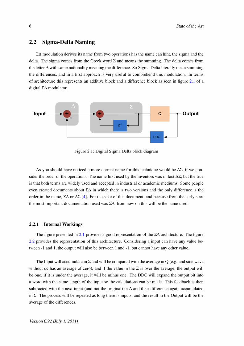
2.2 Sigma-Delta Naming
Σ∆ modulation derives its name from two operations has the name can hint, the sigma and the
delta. The sigma comes from the Greek word Σ and means the summing. The delta comes from
the letter ∆ with same nationality meaning the difference. So Sigma Delta literally mean summing
the differences, and in a first approach is very useful to comprehend this modulation. In terms
of architecture this represents an additive block and a difference block as seen in figure 2.1 of a
digital Σ∆ modulator.
Figure 2.1: Digital Sigma Delta block diagram
As you should have noticed a more correct name for this technique would be ∆Σ, if we con-
sider the order of the operations. The name first used by the inventors was in fact ∆Σ, but the true
is that both terms are widely used and accepted in industrial or academic mediums. Some people
even created documents about Σ∆ in which there is two versions and the only difference is the
order in the name, Σ∆ or ∆Σ [4]. For the sake of this document, and because from the early start
the most important documentation used was Σ∆, from now on this will be the name used.
2.2.1 Internal Workings
The figure presented in 2.1 provides a good representation of the Σ∆ architecture. The figure
2.2 provides the representation of this architecture. Considering a input can have any value be-
tween -1 and 1, the output will also be between 1 and -1, but cannot have any other value.
The Input will accumulate in Σ and will be compared with the average in Q (e.g. and sine wave
without dc has an average of zero), and if the value in the Σ is over the average, the output will
be one, if it is under the average, it will be minus one. The DDC will expand the output bit into
a word with the same length of the input so the calculations can be made. This feedback is then
subtracted with the next input (and not the original) in ∆ and their difference again accumulated
in Σ. The process will be repeated as long there is inputs, and the result in the Output will be the
average of the differences.
Version 0.92 (July 1, 2011)

2.3 The necessity in Oversampling and Conversion 7
Figure 2.2: Internal Workings for the First Order Sigma Delta
2.3 The necessity in Oversampling and Conversion
In modern electronics, computational, signal, sound and video and many others, the process-
ing is done mostly in a digital form. The digital form permits that very complex systems can be
represented by simpler systems that otherwise were very difficult or even impossible to implement
in an analogue version.
Because the exponential growth in the processing speed in the core of computers and systems
alike, the interfaces and the converters with the outside world (That still remains in analogue form)
Version 0.92 (July 1, 2011)
8 State of the Art
must keep up. The core processing speeds raises and so the data acquisition and release must raise
as well.
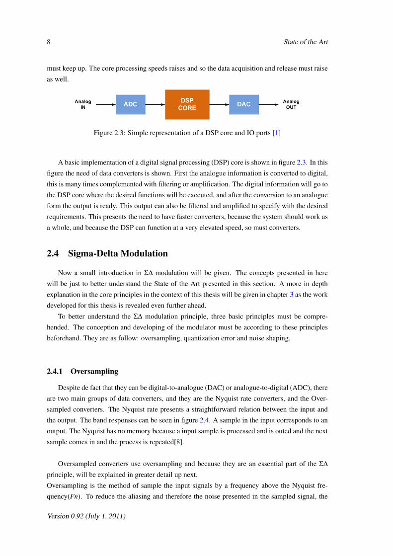
Figure 2.3: Simple representation of a DSP core and IO ports [1]
A basic implementation of a digital signal processing (DSP) core is shown in figure 2.3. In this
figure the need of data converters is shown. First the analogue information is converted to digital,
this is many times complemented with filtering or amplification. The digital information will go to
the DSP core where the desired functions will be executed, and after the conversion to an analogue
form the output is ready. This output can also be filtered and amplified to specify with the desired
requirements. This presents the need to have faster converters, because the system should work as
a whole, and because the DSP can function at a very elevated speed, so must converters.
2.4 Sigma-Delta Modulation
Now a small introduction in Σ∆ modulation will be given. The concepts presented in here
will be just to better understand the State of the Art presented in this section. A more in depth
explanation in the core principles in the context of this thesis will be given in chapter 3 as the work
developed for this thesis is revealed even further ahead.
To better understand the Σ∆ modulation principle, three basic principles must be compre-
hended. The conception and developing of the modulator must be according to these principles
beforehand. They are as follow: oversampling, quantization error and noise shaping.
2.4.1 Oversampling
Despite de fact that they can be digital-to-analogue (DAC) or analogue-to-digital (ADC), there
are two main groups of data converters, and they are the Nyquist rate converters, and the Over-
sampled converters. The Nyquist rate presents a straightforward relation between the input and
the output. The band responses can be seen in figure 2.4. A sample in the input corresponds to an
output. The Nyquist has no memory because a input sample is processed and is outed and the next
sample comes in and the process is repeated[8].
Oversampled converters use oversampling and because they are an essential part of the Σ∆
principle, will be explained in greater detail up next.
Oversampling is the method of sample the input signals by a frequency above the Nyquist fre-
quency(Fn). To reduce the aliasing and therefore the noise presented in the sampled signal, the
Version 0.92 (July 1, 2011)

2.4 Sigma-Delta Modulation 9
sampling frequency (Fs) must be at least two times the input signal. This minimum frequency
required to reduce the aliasing is called the Nyquist frequency. Oversampling is going beyond the
Nyquist frequency for the sampling (equation 2.1). This increase is called the oversampling ratio
(OSR) and it is theoretically unlimited, but the values for OSR are usually factors of two up to
512[3].
OSR =Fsf n
(2.1)
Oversampling has the advantage of reducing the requirements of the prior and the subsequent
stages of the modulation, such as the Anti Aliasing filter (AAF). The aliasing suppression can be
observed in the figure 2.4. In this figure also can be observed that the requirements in the AAF
can be laxed if the oversampling is used, permitting for example that the order of that filter to be
lower.
Figure 2.4: a) Nyquist rate b) oversample rate[2]
A clear and present disadvantage is the increase in power consumption and other parameters
that will be presented later on, specially in section 3.
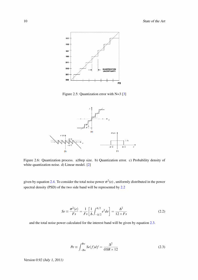
2.4.2 Quantization Error
To a signal to enter a DAC Σ∆ it must be in a digital format. The digital signal presented in the
input is a previous quantized signal. The quantization is simply the act of representing an analogue
signal with its correspondent binary representation, and it is defined by the number of bit used (N).
The number of bits defines the size of the steps used in representing the signal ∆, for example a N
= 3 means 23, which gives a number of 8 steps in representing the signal (see figure 2.5).
Because using a fixed number of steps to represent a infinite number of values, a specific step
may be different that the real value. This uncertainty gives an error in representing the signal
because a digital number cannot represent a full scale analogue one. This quantization uncertainty
(or error, or noise) will be in the worst case equal to half a step and because its uncorrelated
with the input signal level it has a uniform distribution, and can be considered white noise in the
spectrum. Because of this in-correlation the full Power quantization error (Pe) in a spectrum is
Version 0.92 (July 1, 2011)
10 State of the Art
Figure 2.5: Quantization error with N=3 [3]
Figure 2.6: Quantization process. a)Step size. b) Quantization error. c) Probability density ofwhite quantization noise. d) Linear model. [2]
given by equation 2.4. To consider the total noise power σ2(e) , uniformly distributed in the power
spectral density (PSD) of the two side band will be represented by 2.2
Se≡ σ2(e)Fs
=1
Fs
[1∆
∫∆/2
−∆/2e2de
]=
∆2
12×Fs(2.2)
and the total noise power calculated for the interest band will be given by equation 2.3.
Pe≡∫ Bw
−BwSe( f )d f =
∆2
OSR×12(2.3)
Version 0.92 (July 1, 2011)
2.4 Sigma-Delta Modulation 11
And without oversampling (meaning OSR = 1) we have the famous relation given by equation
2.4. Comparing the two, it can be observed that by using oversampling the error (or noise) will be
reduced 3 dB for each octave increase in OSR, by comparison with Nyquist rate converters.
Pe =∆2
12(2.4)
2.4.3 Noise Shaping
Noise shaping is a method of inserting the quantization error in the feedback loop. Because
the negative feedback loop works as a filter, this helps reduce the quantization error that occurs
in every sampling. Because the noise is more spread in the frequency because of the earlier
oversampling, most of the noise created in the process will be filtered in the feedback loop, and
the transfer function of this loop for noise is called the noise transfer function (NTF). This also
means that the higher the number of loops, meaning the order of the modulator (L), the better the
noise reduction will be [9].
For a first order Σ∆ modulator, the NTF in the z-domain will be given by equation 2.5.
NT F(z) = (1− z−1)L (2.5)
Now lets consider that z = e j2π/Fs, OSR greater than one, and Fs = 2OSRBw. Also what was
discussed in 2.4.2 that the ∆ can be taken as white noise. In this case the noise shaped power (Pq)
in the desired band is given by equation 2.6.
Pq≡∫ Bw
−Bw
∆2
12×Fs|NT F( f )|2d f (2.6)
Pq' ∆2
12π2L
(2L+1)OSR2L+1 (2.7)
From the equation 2.7, it can be seen that the noise power Pq, reduces with OSR by 6L dB/oc-
tave more than in equation 2.3. And with this realization an important characteristic Σ∆ is inferred,
with oversampling and noise shaping the reduction in noise is a lot greater that just with oversam-
pling.
2.4.4 Σ∆ Performance
As already presented in the section 1.2, the main objective proposed is to achieve a digital
modulator and SNR of 100 dB. The SNR is the relation between the power of the signal, and the
Version 0.92 (July 1, 2011)
12 State of the Art
power of the noise, hence its representation is favored in dB.
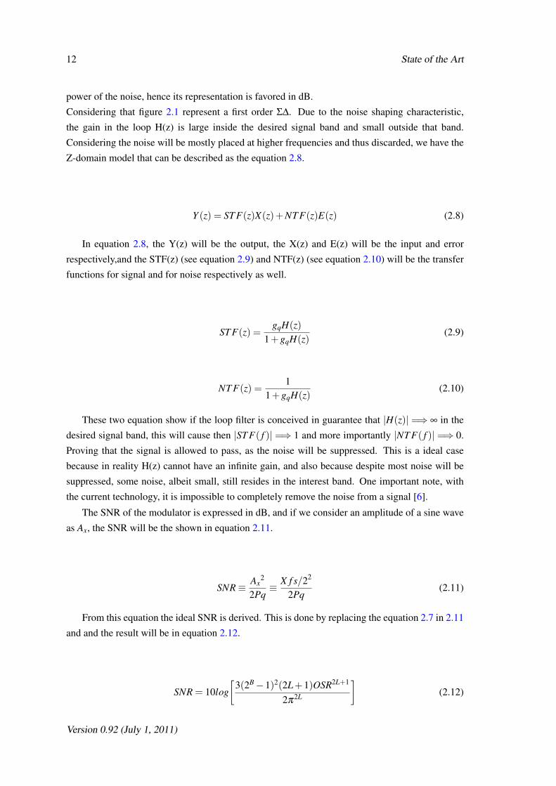
Considering that figure 2.1 represent a first order Σ∆. Due to the noise shaping characteristic,
the gain in the loop H(z) is large inside the desired signal band and small outside that band.
Considering the noise will be mostly placed at higher frequencies and thus discarded, we have the
Z-domain model that can be described as the equation 2.8.
Y (z) = ST F(z)X(z)+NT F(z)E(z) (2.8)
In equation 2.8, the Y(z) will be the output, the X(z) and E(z) will be the input and error
respectively,and the STF(z) (see equation 2.9) and NTF(z) (see equation 2.10) will be the transfer
functions for signal and for noise respectively as well.
ST F(z) =gqH(z)
1+gqH(z)(2.9)
NT F(z) =1
1+gqH(z)(2.10)
These two equation show if the loop filter is conceived in guarantee that |H(z)| =⇒ ∞ in the
desired signal band, this will cause then |ST F( f )| =⇒ 1 and more importantly |NT F( f )| =⇒ 0.
Proving that the signal is allowed to pass, as the noise will be suppressed. This is a ideal case
because in reality H(z) cannot have an infinite gain, and also because despite most noise will be
suppressed, some noise, albeit small, still resides in the interest band. One important note, with
the current technology, it is impossible to completely remove the noise from a signal [6].
The SNR of the modulator is expressed in dB, and if we consider an amplitude of a sine wave
as Ax, the SNR will be the shown in equation 2.11.
SNR≡ Ax2
2Pq≡ X f s/22
2Pq(2.11)
From this equation the ideal SNR is derived. This is done by replacing the equation 2.7 in 2.11
and and the result will be in equation 2.12.
SNR = 10log[
3(2B−1)2(2L+1)OSR2L+1
2π2L
](2.12)
Version 0.92 (July 1, 2011)

2.5 Sigma-Delta Architecture 13
The expression for an ideal N bit Nyquist rate can be achieved by replacing B=N, L=0, and
OSR = 1. This give us the famous expression for the SNR in equation 2.13.
SNR' 6.02N +1.76 (2.13)
Another important parameter is the effective number of bits (ENOB), and this translates as
the number of bits that are needed to achieve the same SNR that an ideal Σ∆. The final ENOB is
expressed in equation 2.15.
ENOB≡ N ' SNR−1.766.02
(2.14)
ENOB≡ log2
[(2B−1)(2L+1)
2π2L
]+ log2(OSR)
[L+
12
](2.15)
The importance of the ENOB will later be explained in the following sections as the work
for this thesis is being shown. Equation 2.14 and 2.15 mean that it can be achieved the same
performance as an ideal Nyquist N bit with an Σ∆ modulator, by combining oversampling and
increase in the loop filter.
2.5 Sigma-Delta Architecture
Now a brief explanation on how a Σ∆ operates in relation to its architecture, will be given.
This explanation will help to understand the concepts already studied and demonstrated, and also
the future work down the road, and thus became vital for this State of The Art.
First we need to comprehend the concept of a Σ∆ modulator. This modulator permits the en-
coding of signals with high resolution into signals with less resolution, all without losing quality
[6] . The internal function of a Σ∆ will be more easily understood, after a detailed breakdown.
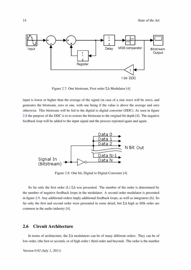
As seen in figure 2.7, a digital Σ∆ is comprised of one input, and one output. The "Digital in",
is the input signal to be modulated. The "Bitstream" is the digital output of the resulting modulated
signal. Please note that the input signal can be one or more in bit depth.
First the input signal, will pass by the register and according to the clock will be stored and
added again in the register, this will act like an integrator. Later the comparator compares if the
Version 0.92 (July 1, 2011)
14 State of the Art
Figure 2.7: One bitstream, First order Σ∆ Modulator [4]
input is lower or higher than the average of the signal (in case of a sine wave will be zero), and
generates the bitstream, zero or one, with one being if the value is above the average and zero
otherwise. This bitstream will be fed to the digital to digital converter (DDC). As seen in figure
2.8 the purpose of the DDC is to to restore the bitstream to the original bit depth [4]. The negative
feedback loop will be added to the input signal and the process repeated again and again.
Figure 2.8: One bit, Digital to Digital Converter [4]
So far only the first order (L) Σ∆ was presented. The number of the order is determined by
the number of negative feedback loops in the modulator. A second order modulator is presented
in figure 2.9. Any additional orders imply additional feedback loops, as well as integrators [6]. So
far only the first and second order were presented in some detail, but Σ∆ high as fifth order are
common in the audio industry [4].
2.6 Circuit Architecture
In terms of architecture, the Σ∆ modulators can be of many different orders. They can be of
low order, (the first or second), or of high order ( third order and beyond). The order is the number
Version 0.92 (July 1, 2011)

2.7 Circuit Design 15
Figure 2.9: One bitstream, Second order Σ∆ Modulator
of closed feedback loops in the architecture. As demonstrated in 2.4.3 the order will also represent
the parameters in the NTF that will reduce the noise in the interest band. In theory, there is no
limit for a high order, and any number could be achieved, but in practice the stability is greatly
reduced, rendering the Σ∆ impractical to design.
2.6.1 Stability
As late as the 80’s many engineers believed that any order above two, was hopeless to stabilize
[10]. Advances in Σ∆ technology, in design and in architecture, proved this wrong. Still the
stability of Σ∆ modulators is still a problem in higher orders. Usually Σ∆ modulators will not be
any higher than the sixth order. This was demonstrated by R. Schreier in a very comprehensive
study done in the late 90’s [11].
2.7 Circuit Design
The recent advances in CMOS circuit design, provide many possibilities in terms of develop-
ment and implementation in electronics. This is one of the possible recognitions of the Moore’s
Law. Still, new problems have arise in the recent years with the drastic increase in the transistors
density on chip. For example the power consumption can increase with more and more density in
the integrated circuit [12]. Cost is also a factor in determining the architecture. A greater order can
be a specific solution, but a greater order will need more components and that occupies essential
and expensive space on chip.
2.7.1 Power Consumption
In the next table 2.1 several solutions by many research teams will be presented. They compare
the SNR, with the OSR and also the CMOS technology used in the fabrication, to determine a given
Version 0.92 (July 1, 2011)

16 State of the Art
power consumption. The power presented is only for the Σ∆ modulator, and excludes additional
components that can be needed in some of the solutions presented in here.
Ref. SNR (db) OSR l (nm) Pw (mw)[13] 84.8 100 180 0.04[14] 71.0 64 180 0.42[15] 75.2 64 180 0.08
80.6 520[16] 61.4 104 130 1.28
50.5 52[17] 83.0 50 130 0.06[18] 88.4 100 90 0.13
Table 2.1: Σ∆ Power Comparison for Different Technologies
As shown in the table 2.1 a reduction in the technology for the fabrication is not a guarantee
of a less consuming circuit. The reverse cannot also be inferred, in fact many other factors are of
great importance as well. The OSR is also of very importance, a greater oversampling ratio, will
mean more operations must be made by the modulator, and thus more power will be consumed.
2.8 Conclusions
As shown in this chapter, Σ∆ modulation, is nowadays more and more used in many applica-
tions. The combination of higher orders, greater OSR permitted a great increase in Σ∆ uses and
performance. The present report also shown some problems with this technology, but also the
solutions for some of them. Advances in circuit design technology and in architecture permitted
in time the overcoming of many of the intrinsic challenges. This advances will surely be used
in the future with the new problems that will arise with the increase in transistor density and the
subsequent reduction in the tech nodes.
Version 0.92 (July 1, 2011)

Chapter 3
Σ∆ Modulation
As will be explained later on in section 2.5, many specific concepts and parameters must be
first understood and worked upon. First of all a comprehensive study is always needed to devise
a good model or solution. Later a validation and verification of the model obtained must occur.
To better reach this result several simulations are needed to define and also refine those parameters.
The first steps in creating a Σ∆ modulator were in the theoretical study of the proposed solu-
tion. After those several simulations were made, and in this case all were made using MATLAB
and specially the Fdatool and Simulink tools. These tools provided a good environment in sim-
ulating and validating the results and architectures needed in reaching the goal of this thesis, the
100 dB in SNR as explained in section 1.2.
3.1 Theoretical Study
Sigma-Delta modulation is a technique first idealized in the 1960’s. Despite its few decades
in existence, only in the 1980’s with the advent of more advanced silicon fabrication processes,
this modulation became more widespread [7]. Still information about Σ∆ is somewhat limited and
many times lacking in depth in the fundamental explanation. A great portion of the initial work
was to define and study essential parameters that now will be shown.
3.1.1 ENOB
One of the objectives for the thesis as indicated earlier is the implementation of the digital Σ∆
modulator with 18 bits in the input while at the same time also achieving the 100 dB. To guarantee
that it is possible the equation described in 2.14 was used. With an SNR = 100 dB we have the
following equation 3.2.
17

18 Σ∆ Modulation
ENOB≡ N ' SNR−1.766.02
' 100−1.766.02
(3.1)
' 16.32 < 18 (3.2)
With 18 bits the objective of 100 dB is in reach, even with Nyquist rate conversion. Later sim-
ulations for calculating the SNR using Simulink and the quantization parameters will be presented
in subsection 4.1.
3.1.2 Modulator Architectures
Of the first considerations to be determined when developing a Sigma-Delta modulator, one of
them is to establish its order. The order of the modulator is simply the number of feedback loops
present. One feedback loop is the simplest, making it a first order modulator, two feedback loops
make a second order modulator and so on.
To reach 100 dB in SNR a great number of combinations between low and high order, and
one or greater OSR are possible. For this thesis and because the commercial background it may
display, only will be considered the common orders for digital Σ∆ modulators already covered
in the State of the Art. This will simplify the possible stability problems already mentioned in
subsection 2.6.1. The same line of thought is used in choosing the OSR as will be concluded in
section 5.
For the most common architectures and OSR values, they range from order one to five, and
range in OSR from eigth up to 512.
L / OSR 8 16 32 64 128 2561 20 30 40 50 60 702 31 48 63 80 100 1123 42 63 84 105 128 1504 50 78 105 130 160 1855 60 94 128 160 190 219
Table 3.1: SNR in dB according to L and OSR [4]
With the table 3.1, some conclusions can be made. For example, the modulators with an order
equal to one are almost discarded. The SNR of 100 dB is not attainable with L = 1 at least with
the expected values of OSR, greater values could be used, but it would be needed at least 2048 for
OSR to reach 100 dB. The value of 2048 while it is possible to achieve in modern DSP cores and
in simulations using MATLAB but in reality this would be impractical. To use 2048 this would
mean that the modulator will be working with an internal clock of 2048 times faster than the Fs
Version 0.92 (July 1, 2011)

3.1 Theoretical Study 19
used. Because this is an modulator for use in audio, Fs will be the standard of 44100 Hz the same
used in Compact Disc technology. With 44100 times 2048, we reach a value of at least 90 MHz
for the internal clock, and while is not impossible, is very demanding in power consumption for
modern circuits [8].
Please note that increasing the order can potentially reach this objective even with a low OSR,
and that may direct a developer to choose a simpler solution. A low order Σ∆ means less parts, a
more simple architecture, a smaller area to be fabricated and therefore less expensive, thus mak-
ing very desirable. In fact this application of Occam’s razor to electronics is however misleading,
because for a low order to reach a certain SNR, a greater oversampling is required, thus increasing
the power consumption [4]. This is one of the many tradeoffs that a developer or engineer will
face when working in Σ∆ technology. Other tradeoffs will be presented in more detail in chapter
3 and in chapter 5.
Another fact observed in table 3.1 is that with a greater order, the increase in SNR is more
accentuated with the increase in OSR, this was already demonstrated in section 2.4.3. That means
that with a greater order a smaller increase in OSR could suffice in reaching the desired SNR.
The observation of table 3.1 also gives us the following clues in determining the desired Ar-
chitecture. They are as follow:
• With L = 2, there would be needed at least an OSR of 128;
• With L = 3, there would be needed at least an OSR of 64;
• With L = 4, there would be needed at least an OSR of 32 and a maximum of 64;
• With L = 5, an OSR of 32 would be more than enough;
As refered in section 2.6.1, a low order (meaning an order smaller than three, third or above is
called high order), is desirable because of stability problems. With the proposed interval of OSR
between 1 and 256, only a second order modulator with an OSR of 128 at the very least would
be sufficient. If in the later studies and simulations the objective in SNR is not reached, then the
order will be increased. This difference between the theoretical values and the practical ones, are
due to most of the calculations rely on ideal models for the theory, and because the second order
with an OSR of 128 is so close to the minimum objective, the values can differ, and a little change
can make the 100 dB out of reach.
3.1.3 Techniques to increase the SNR
With the aspects of the Σ∆ already presented, a few techniques can be easily devised to increase
the SNR. These strategies are not exclusive or complementary, but a choice of one can alter the
importance of another. The two basic strategies are as follow:
Version 0.92 (July 1, 2011)

20 Σ∆ Modulation
• Increase the OSR.
Simpler to implement, but leads to a great increase in the power requirements.
• Increase the Order.
Very effective, more complex to implement and increase the overall area for the circuit.
One aspect that must be taken into account, is the area versus consumption parameter. A
greater area is most of the times discouraged, but a small increase in area may represent a great
decrease in power consumption. Based in the simplicity of the circuit and in the typical range
for OSR, so far a second order is the most promising architecture [3]. It should be noted that the
choice in technology for the fabrication can change the importance that a given factor can have.
For example, in a smaller technology, the increase in the area may not be that relevant, but the
expected increase in oversampling will cause a greater power consumption because the dynamic
power consumption will be a more important characteristic than in a bigger tech node technology.
The implementation of a higher SNR will imply the choosing and compromising between
these trade-offs.
3.1.4 Noise Power Level
Because one of the desired parameters is to reach 100 dB of SNR and that translates to the Sig-
nal Power in dB over the Noise Power in dB, is imperative to reduce the noise the most as possible.
As demonstrated in section 2.4.2, any signal that is quantized will have an error originated in the
conversion from analogue to digital. Because that error depends on ∆ defined by the equation 3.3.
∆ =I−OVoltageLevel
TotalQuantizationIntervals(3.3)
In equation 3.3, the I-O Voltage Level is the voltage reference of the input wave, meaning its
amplitude, and the Total Quantization Intervals are the number of intervals that are defined by the
number of bits (N) in the quantization (2N). Therefor we have in equation 3.4 the voltage that each
interval comprises. This means that for a given input level the ∆ will be different, for an example
of a wave with 5 Volts in amplitude we have the following equation.
∆ =5V218 = 19.07uV (3.4)
This poses another challenge because a choice in a certain technology can infer the level of the
noise. In table 3.2 the most common technologies available by Europractice at FEUP. This table
also presents the voltage I-O voltage levels and the expected noise power in dB of those same
Version 0.92 (July 1, 2011)

3.2 Signal Modulation 21
levels after a quantization of 18 bits.
Tech I-O voltage Level (V) ∆ (uV) Noise Power (dB)AMS 350 [19] 5.5 20.98 -104.35TSMC 180 [20] 3.3 12.59 -108.79UMC 130 [21] 3.3 12.59 -108.79UMC 90 [22] 3.3 12.59 -108.79
Table 3.2: Noise Power of 18 bits quantization by Technology I-O input levels
The table 3.2 and to some extent equation 3.3, shows that in general a low tech is desirable
because of a lower level of noise power. Also shows that with low technologies and 18 bit reso-
lution the most deviation in the input will be very small. For example for UMC 90, this means a
maximum deviation of half the ∆ interval, meaning 6.3 u V which is very difficult to achieve in a
regular modulator without expensive coupling components [6]. In regard to the noise power being
small in lower technologies, this maybe untrue because with a lower Input Level the signal is also
lower and that means a not so significant change in the relation between the two of them (hence
the SNR). The specific relation will be made later on.
One final note about this subsection must be made before moving foward. The secundary
objectives for this dissertation state that the physical implementation must be possible to achieve
in a digital circuit. This may cause some confusion as to the need of this last subsection because if
the implementation is fully digital, then there is no need to consider the quantization of a analogue
input, because the signals in digital form have very defined states. In reality there could be a need
to implement a complete sound processing core in a circuit, with the correspondent analogue input
and even analogue output. In this case the information presented in here is not expendable, and
will be important in choosing the fabrication technology.
3.2 Signal Modulation
Sigma Delta audio modulators share in common some very specific blocks, as can be seen in
figure 3.1. The blocks are as follow: IF is the interpolation filter, NL is the Noise Shaping Loop
(NSL), DAC is the Digital to Analogue Converter and finally the LPF is the Analogue Lowpass
Filter. For the scope of this thesis only the digital part is the objective, the analogue part is to
present the full components of the DAC modulator.
In this figure 3.1 it can also be seen the path the data travels through the DAC. First a bitstream
with a bit depth of N0 (in this thesis will be 18 bits) will pass through the IF. After interpolated and
raised its frequency to the desired OSR, the data will enter the NSL where it will be modulated.
The output of the NSL will be a bitstream of 1 bit in depth with the same frequency of the NSL
input, ready to be converted to an analogue signal by the DAC, and the final LPF will only present
Version 0.92 (July 1, 2011)

22 Σ∆ Modulation
Figure 3.1: Building blocks for a full DAC architecture [5]
the desired band for audio. This band follows the audio perception capabilities for the human ear,
ranging from 20 to 20000 Hz [23].
3.2.1 Wave Modulation
In Sigma Delta, the difference (∆) is added to the input (Σ), hence its name. To better com-
prehend this concept, in figure 3.2 will be shown the input wave and the output bitstream. In this
demonstration the input wave is a sine wave that was quantized to 7 bits just for simplicity reasons.
A wave quantized with 7 bits, means 128 steps making it still possible to observe each step and
resulting output bitstream. The final input wave of the proposed modulator will be quantized by
18 bits to correspond to the objectives specifications. Every result presented now was simulated
using a first order Σ∆ modulator in Verilog language, and was simulated using the Cadence Ncsim
software, and the waveforms were extracted using Cadence Simvision software. The letters A
and B are shown next to the figures 3.2, 3.3 and 3.4, with A representing the Input wave, and B
representing the output bitstream.
Figure 3.2: Input wave and resulting Bitstream for an OSR = 1
In the figure 3.2, can clearly be observed the modulation result in the output. When the wave
is in the maximum of the positive swing the bitstream is mostly one. As it goes down in amplitude
the bitstream will slowly have more zeros until it reaches the average value. In zero of the input
wave, the bitstream is comprised with an equal number of zeros and ones. If the input wave goes
to the negative swing the output, as it goes down, will be more and more zeros until is mostly zero
in the minimum. Afterward, as the wave goes back up but while still in the negative swing the
ones appear but the bitstream is still mostly zeros. When the wave resurfaces to zero the number
Version 0.92 (July 1, 2011)

3.2 Signal Modulation 23
of zeros is again the same as the number of ones, and the process is repeated again.
In figure 3.2, the OSR is one, meaning that to each sample of the input wave there is a output
signal. If the OSR is two, as seen in figure 3.3, each sample is processed two times before a new
one enters, and the output bitstream still displays the same behavior. Despite the same behavior,
the bitstream is now more fast and carries more resolution, this is very useful when in the later
stages of this thesis, the bitstream is again reconstructed to an analogue signal.
Figure 3.3: Input wave and resulting Bitstream for an OSR = 2
For comparison purposes now the same simulation will be presented for an OSR = 4. This
result is presented in the 3.4 figure. At first glance the output wave appears to have more ones than
zeros, specially in the zones where the input wave is zero (meaning an average of zero as well).
In reality the number of zeros is the same as the number of ones, but for this level of zoom the
transitions cannot be correctly displayed. Still the same behavior can be observed outside those
zones, but with an increase of the samples as expected.
Figure 3.4: Input wave and resulting Bitstream for an OSR = 4
3.2.2 Wave modulation in the data path
Now the behavior of the full modulator for a first order is presented to better comprehend the
circuit. Using as reference the circuit in figure 3.5, a first order was simulated using the same
specifications used in 3.2.1, the behavior in the error and in the accumulator is displayed in figure
Version 0.92 (July 1, 2011)
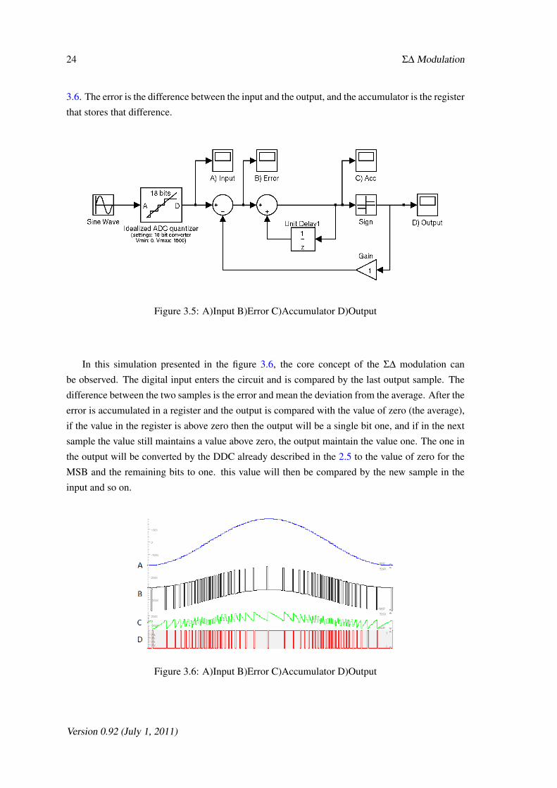
24 Σ∆ Modulation
3.6. The error is the difference between the input and the output, and the accumulator is the register
that stores that difference.
Figure 3.5: A)Input B)Error C)Accumulator D)Output
In this simulation presented in the figure 3.6, the core concept of the Σ∆ modulation can
be observed. The digital input enters the circuit and is compared by the last output sample. The
difference between the two samples is the error and mean the deviation from the average. After the
error is accumulated in a register and the output is compared with the value of zero (the average),
if the value in the register is above zero then the output will be a single bit one, and if in the next
sample the value still maintains a value above zero, the output maintain the value one. The one in
the output will be converted by the DDC already described in the 2.5 to the value of zero for the
MSB and the remaining bits to one. this value will then be compared by the new sample in the
input and so on.
Figure 3.6: A)Input B)Error C)Accumulator D)Output
Version 0.92 (July 1, 2011)

3.3 Interpolation Filter 25
3.3 Interpolation Filter
The first block to be implemented as part of the proposed solution, is the Interpolation Filter,
this is shown in the figure 3.1. The interpolation filter will increase the sampling frequency from
the Nyquist to the OSR, this is a crucial step because the oversampled converter, as explained in
section 2.4.1, works by the increase of the input sampling frequency. Another important action
realized by the interpolation filter is to remove the spectral replicas centered at the Nyquist multi-
ples. This filtering of the replicas is crucial because sampling at a given frequency Fs, will cause
images replicas centered at Fs, 2Fs, 4Fs, until (OSR -1)Fs.
3.3.1 The need for interpolation
One can in theory increase the sampling frequency rapidly to OSR×Fn and then filter every-
thing outside the desired band. The problem with this approach is that a large amount of power
would be lost by the IF functioning at high speed. The core principle of interpolation is that in
an input are inserted more samples in between with the value zero. This operation is called zero-
padding (in some literature the same process is called zero-stuffing) [24]. Next the signal is filtered
to remove the images replicas around the multiples of the new sample frequency. If an ideal filter
were used it would have a very sharp response in cutting the undesired band, or as commonly
called a brick-wall effect. In reality the new steps in filtering will introduce some errors that must
be accounted for in the later stages.
3.3.2 Interpolation Filter for Σ∆ DAC
As seen in the figure 3.1 the interpolation filter could be composed by a single filter inter-
polating the data by the required number of times in OSR. The reality is that a filter with such
characteristics will present a very high order and will be very cumbersome to design and fabricate
in terms of area. The order represents in the filter the number of taps which are related to the mul-
tipliers and the adders needed, and all those components require a great deal of area. To reduce the
space requirements is very useful to separate the filter is several stages which in total will have a
lesser area than one single filter, that separation process will be presented in the subsection 3.3.4.
3.3.3 FIR versus IIR Filters
A single stage Interpolation filter with an interpolation factor of OSR will have very large
requirements in terms of area. For example if an OSR of 128 is chosen the requirements are
presented in the table 3.3. The filter presented in here are the most common used in interpolation
filters [24]. All the simulations used in the next table were made using the Fdatool from MATLAB.
The simulations were for an OSR of 128, meaning a sample frequency of 128× 44100Hz =5644800Hz, and with a transition band of 20000 Hz and a stopband of 22050 Hz. These require-
ments are standard for human audition [25]. At a first glance the order requirements don’t appear
Version 0.92 (July 1, 2011)

26 Σ∆ Modulation
Filter Type OrderFIR Kaiser 17655
FIR Equiripple 8498IIR Butterworth 120IRR Chebyshev 29
IRR Eliptic 14
Table 3.3: Filter Order in Single Stage for FIR and IIR
very demanding, but that is only true if we consider also the IIR filters as reliable. For audio im-
plementations IIR filters are a very bad choice because the phase response. This limits the possible
choices to FIR filters, but these filters are very demanding in area, and deemed impractical.
As an example for the comparison between FIR and IIR, consider the next figures in 3.7 and
3.8. A filter with an Fs of 44100Hz and the same stopband and transition bands as the simulations
presented in table 3.3 were used. The filters response were also simulated using the Fdatool.
Figure 3.7: Magnitude and Phase response for a FIR Equiripple filter
Version 0.92 (July 1, 2011)

3.3 Interpolation Filter 27
In the figure 3.7, the Magnitude and Phase response are presented for a FIR Equiripple. An
Equiripple was simulated because from all the FIR filters it presented the lower order from those
simulated in 3.3. This filter is used as an example and has a order of 155, and as seen and explained
in subsection 3.3.4 it will be very important in the interpolation filter.
In the figure 3.8, the Magnitude and Phase response are presented for a IIR Elliptic. An
Equiripple was simulated because it presented the lower order from the IIR simulated in 3.3. Both
the FIR and the IIR present very good brick wall characteristics, corresponding to a very sharp
magnitude response. Despite the somewhat similar response in gain, the phase response is very
different. The FIR presents a linear phase response and the IIR phase response is not linear, thus
making it very unrecommended for audio applications [26]. This fact brings the conclusion that
despite the very promising gain in area versus the FIR, the IIR is not a good choice for interpola-
tion filters.
Figure 3.8: Magnitude and Phase responce for a IIR Elliptical filter
3.3.4 Designing a cascade Interpolation Filter
As seen in subsection 3.3.2 one stage interpolation filter can be very demanding in area. To
address this problem the interpolation filter can be divided in smaller stages, and the overall area
Version 0.92 (July 1, 2011)

28 Σ∆ Modulation
of all the stages combined is still smaller than the original one. An idea of how the separation
is made is presented in the figure 3.9. The calculations in the specific orders for each stage and
said parameters are very complex, one prime example for that complexity is the Parks-McClellan
Algorithm [27], therefore in this subsection, a simpler process to achieve acceptable results will
be now presented.
Figure 3.9: Cascaded Interpolation Filter [6]
When first starting with any given band, the sampling of that band will create a spectral replica
centered around the sample frequency (Fs). These replicas can create distortion created by the
aliasing if the Nyquist theorem is not respected. To eliminate the undesired replicas, a precise
filter is needed to cut out anything above the desired band.
Using the specifications in this thesis of Fs=44100 Hz, a band transition band of 20000 Hz,
and a stopband of 22050 Hz. The first stages will be Interpolation Filters that interpolate by two
times the input values, meaning if they receive a bitstream of say 10 words in a period of 10 nano
seconds, the output will be 20 words, in the same duration.
Figure 3.10: Spectrum of the Input on the Interpolation filter
For this modulator to be capable of integration with audio applications, it must be capable of
operating with bands ranging in frequency from 20 Hz up to 20000 Hz, and this fact also applies
Version 0.92 (July 1, 2011)

3.3 Interpolation Filter 29
to the interpolation filter. A signal evenly distributed with a band of 20000 Hz, if sampled at a
Fs of 44100 Hz, will display a spectrum as show in figure 3.10. This figure is a theoretical repre-
sentation of the expected spectrum. The band of 20000 Hz will be replicated around the integer
multiples of Fs ( 2FS, 3FS, 4FS, and so on). Because the desired band ends at 20000 Hz, and the
replica starts at 22050 Hz, the interval for the filter to operate is very small. As can be seen the
first filter will have to have a very sharp cutoff characteristic. To cut all the replicas above the Fs/2,
and then later interpolate the data to the new sampling frequency of 2 times the original one. This
represents a FIR filter with the characteristics in table 3.4.
The images presented for the spectrum are emulations of the output spectrum for each filter
and therefore are theoretical models. This method of presenting the spectrum is used because it is
necessary to shown the several replicas up to at least 8Fs (the last spectral replica to be removed,
and the MATLAB models only permit to visualize up to 2 Fs.
Using the aforementioned Fdatool, the frequency response was calculated and the filter pa-
rameters extracted. The result for the first stage filter was already presented in the figure 3.7
because the simulations parameters were the same. In fact the example presented the figure 3.7,
was exactly the same for the first stage, just for simplicity reasons, and to prevent several similar
images.
Type FIR Filter EquirippleFs 44100 Hz
Transition Band 20000 HzStopband 22050 Hz
Attenuation 100 dBOrder 155
Table 3.4: First Stage Filter Characteristics
Applying the frequency response of the first filter to the spectrum of the input sampled band,
the filter will remove every spectral replicas over the band of 20000 Hz. This can only happen
because the filter has a very sharp cutoff characteristic, almost a brick-wall effect. Because the
filter is interpolating the data with a new Fs that is the double of the original sample frequency,
every odd-order image is suppressed. So now the spectral image of the remaining band is with the
original band and the even order bands. This spectral filtering is presented in the figure 3.11.
Now the original digital input was interpolated and is at the double of the original sample fre-
quency. Because an typical OSR can reach values as high as 512 [3], and the objective of 128 is
presented to verify if an SNR of 100 dB can be achieved, another interpolation must be made.
Version 0.92 (July 1, 2011)

30 Σ∆ Modulation
Figure 3.11: Spectrum of the output of the first stage
The second filter must also remove every signal above the original band of 20000 Hz, but
now the transition band and the stopband have more relaxed parameters that in the first filter. The
original interval between the transition and the stopband was only of 2050 Hz (22050 Hz - 20000
Hz). After the first interpolation filter the interval is of the new stopband minus the original band,
meaning 44100 Hz - 20000 Hz = 24100 Hz. It is this increase in interval that permits the second
filter to have a smaller order than the first and it is the key to the entire process of separating and
cascading Interpolation filters. The second filter characteristics are now presented in the table 3.5
and the frequency response is presented in figure 3.12.
Type FIR Filter EquirippleFs 88200 Hz
Transition Band 20000 HzStopband 44100 Hz
Attenuation 100 dBOrder 23
Table 3.5: Second Stage Filter Characteristics
Now the original digital input is interpolated and is four times the original sample frequency.
The output spectrum is now presented in figure 3.13.
The process now is again repeated. The original signal is still interpolated by four, and for
this example 128 are needed. A third stage filter is again needed. The filter must remove the
replicas above the original band of 20000 Hz. The Fs will now be 176400 Hz the transition band
will the already mentioned 20000 Hz, and the stopband will be 88000 Hz. The parameters for the
Version 0.92 (July 1, 2011)

3.3 Interpolation Filter 31
Figure 3.12: Magnitude and Phase response for the second stage Equiripple filter
Figure 3.13: Spectrum of the output of the second stage
Version 0.92 (July 1, 2011)
32 Σ∆ Modulation
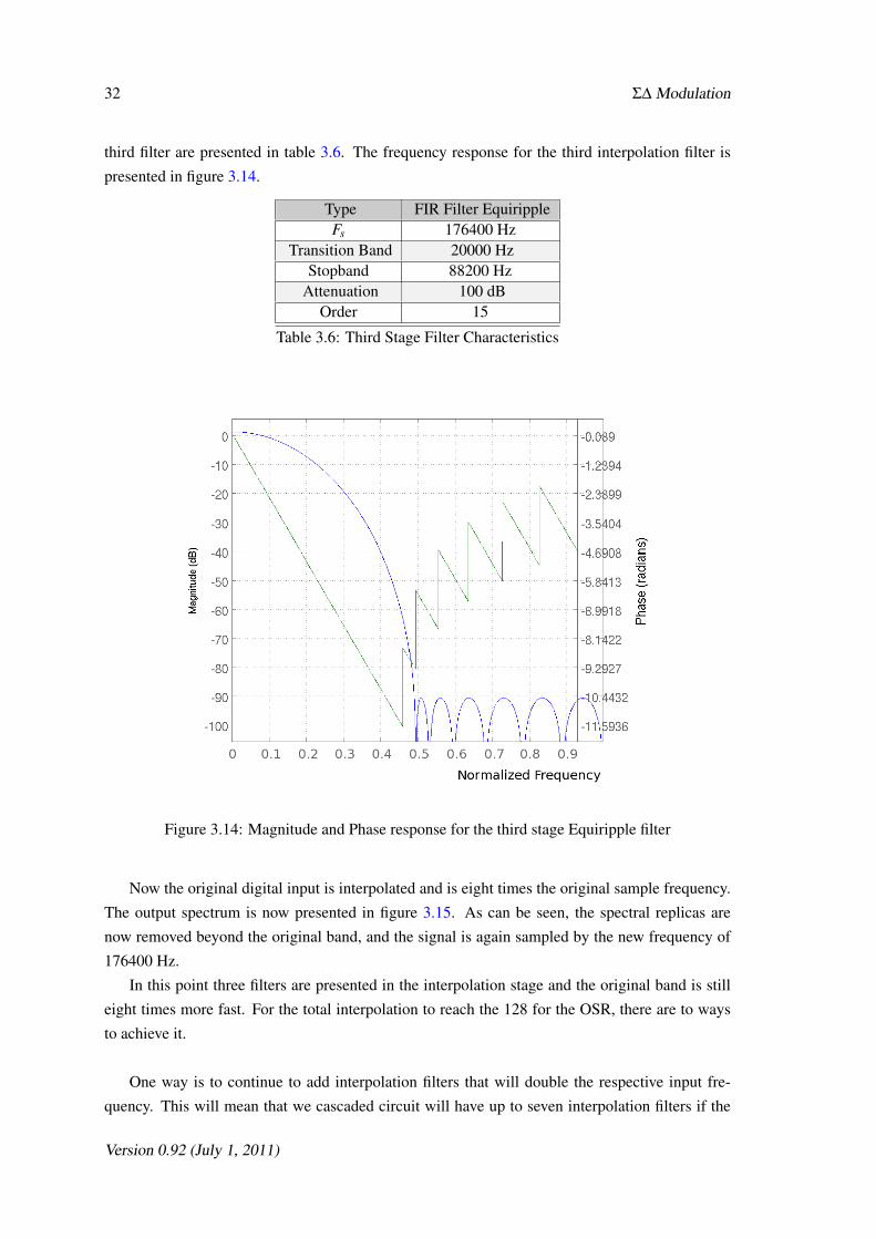
third filter are presented in table 3.6. The frequency response for the third interpolation filter is
presented in figure 3.14.
Type FIR Filter EquirippleFs 176400 Hz
Transition Band 20000 HzStopband 88200 Hz
Attenuation 100 dBOrder 15
Table 3.6: Third Stage Filter Characteristics
Figure 3.14: Magnitude and Phase response for the third stage Equiripple filter
Now the original digital input is interpolated and is eight times the original sample frequency.
The output spectrum is now presented in figure 3.15. As can be seen, the spectral replicas are
now removed beyond the original band, and the signal is again sampled by the new frequency of
176400 Hz.
In this point three filters are presented in the interpolation stage and the original band is still
eight times more fast. For the total interpolation to reach the 128 for the OSR, there are to ways
to achieve it.
One way is to continue to add interpolation filters that will double the respective input fre-
quency. This will mean that we cascaded circuit will have up to seven interpolation filters if the
Version 0.92 (July 1, 2011)

3.3 Interpolation Filter 33
Figure 3.15: Spectrum of the output of the third stage
OSR is 128 (27 = 128). If the desired OSR is 256 interpolation will be made by eight filters and
so on. The remaining filters are still calculated by same method used in calculating the second and
third interpolation filter. This way bring the problems of delays in the circuit and will consume
allot of power in the overall.
Another way is to replace the fourth and the subsequent filters by a single Sample and Holder
(S/H) with the interpolation factor that still remains. The S/H is just like the FIR filters, linear in
phase so this makes them suitable for audio applications. The interpolation made by a S/H has a
response in frequency similar to a sinc(x) function. The characteristics for the S/H are presented
in table 3.7 and the frequency response is presented in the figure 3.16.
Type Sample and HoldFs 2822400 Hz
Transition Band 20000 HzStopband 282240 Hz
Attenuation 100 dBOrder 140
Interpolation 16
Table 3.7: Sample and Hold Filter Characteristics
The presented sample and hold has an order of 140. this means that even with more compo-
nents, the sum of them all will still represent a lower number than a simple one with and very large
interpolation factor. The total in order is now given by equation 3.6, and each FILT ERi represents
Version 0.92 (July 1, 2011)

34 Σ∆ Modulation
Figure 3.16: Magnitude and Phase response for the 16 times interpolation S/H
the order of the filter where i is the index of the filter. The reduction is very significant, and despite
more complex in design, there is great advantages in using this method. The final spectrum on
the output of the S/H is presented in the figure 3.17, and it shows the same input band, but now
interpolated by the OSR of 128.
Figure 3.17: Output spectrum of the Cascaded Interpolation Filter
Version 0.92 (July 1, 2011)
3.4 Conclusions 35
FILT ER1 +FILT ER2 +FILT ER3 +FILT ER4 = Totalorder (3.5)
155+23+15+140 = 333� 8498 (3.6)
If the desired OSR is above 8 and different of 128, a different S/H is needed. It is the only
thing that needs to be changed using this design technique, and all the other components of the
interpolation filter remain the same, and all the design techniques so far shown are still to be
followed. Next the table 3.8 shows the order of the S/H, the desired OSR and the total order of the
interpolation filter using the equation 3.6 by replacing the respective S/H order and calculating the
total order.
OSR S/H Interpolation factor S/H order Total order32 4 60 25364 8 86 279
128 16 140 333256 32 165 358512 64 180 373
Table 3.8: OSR, S/H interpolation factor and order, Total order
3.4 Conclusions
So far it was presented the preliminary study to implement the Σ∆ modulator. To permit the
use of this modulator as a component of a DAC converter for audio applications as defined by the
objectives, a interpolation filter was designed. To attain a interpolation filter as less cumbersome
in terms of area as possible, a method for separating a larger filter into smaller ones in which the
sum of them all is still smaller the original, was also presented and simulated.
If a simple a design approach is used, the calculations done so far point that a second order
modulator with an OSR of 128 is capable of reaching a SNR of 100 dB with 18 bits in the in-
put. In the next chapter the implementation of the proposed solution will be made following the
guidelines presented in this chapter. If the SNR is insufficient, then a new OSR may be needed,
and that implies by the method presented in subsection 3.3.4, a redesigning of the last stage of the
cascaded interpolation filter.
To fully implement the modulator, in the next chapter two main routes will be taken, first a de-
tailed Simulink tests and validation of the performance parameters, and later the presented solution
in the Verilog HDL language will also be simulated to guarantee the objectives were accomplished.
Version 0.92 (July 1, 2011)

36 Σ∆ Modulation
Version 0.92 (July 1, 2011)

Chapter 4
Digital Σ∆ Modulator
In this chapter, the proposed Σ∆ Modulator will be presented. The methods for the design and
simulation for the solution are to demonstrate the modulator performance, in the SNR and in the
18 bits input, which are the main objectives. The architecture presented in this chapter was first re-
alized in the Simulink environment and simulated, and later the modulated was realized in Verilog
language and the expected results verified through a verification process later demonstrated.
4.1 MATLAB Simulation
After the decision for the second order and the subsequent choice for the OSR, the following
architecture was realized in Simulink environment. This architecture was realized to verify if the
SNR could reach the 100 dB, and also the dynamic parameters that will be discussed in more detail
in 4.1.3. For this process and because the main interpolation filter was already studied in depth in
the cascading of the filters (see chapter 3.3), the focus of the simulations were in the modulator in
particular.
4.1.1 Simulated Modulator
In figure 4.1 the second order modulator is presented. The Main parts are the NSL1, the NSL2
and the Signal extractor. The purpose of the NSL1 and the NSL2 are to accumulate the errors
presented in their respective inputs and to compared them with the next input values, thus making
them the feedback loop. The Signal Extractor is simply to compare the value on the output of
the second accumulator. Because the signal is a specific number of bits in a signed form. The
theoretical quantizer, compared if the value is greater than the value of zero, but in the simulations
removing the MSB and pass the complement through the bitstream. The Unit Delay before the
Signal Extractor is simply to prevent the data to be in a single combinatorial path that will deny the
simulation to occur. The difference between this implementation and the second order seen in the
specialized literature is the use of a signal extractor instead of the comparator, and the unit delay
37

38 Digital Σ∆ Modulator
after the NSL2 and not in the feedback loop as often found. Both of these changes were made to
ease the simulations, the extractor is a simpler implementation comparing to a MSB comparator
and the Unit Delay prevents the simulator to have undefined states that undermines the solution.
Figure 4.1: Second Order Implementation
4.1.2 SNR in the Input
To guarantee that a given signal has an SNR of 100 dB in the output, the input signal must
be studied in detail. In chapter 3.1.1 the equation that related the SNR with the number of bits
was presented in 3.2. The calculated value for 18 bits was SNR = 110. Because the SNR is the
Power of the Signal over the Power of the noise a effective way to verify the 18 bits feasibility is
to measure the power of the input wave, modulate the wave and measure the power of the noise.
SNRdB = 20× log10
(SignalPowerNoisePower
)= 20× log10
(RMSSignal
RMSNoise
)(4.1)
The RMS is the root mean square of the wave or signal, and its value is extracted from the
Simulink. The circuit and the extraction is presented in the figure 4.2. The method is that first
a sine wave with an amplitude of 217 is quantized to the ENOB to be measured, in this case 18
bits. Next the output of the quantized is subtracted to the input and this gives the error inserted
by the quantizer and that error is the passed through by the RMS block. The signal without the
error is obtained by subtracting the output of the quantizer with the previously obtained error, and
afterward pass it through a RMS block as well.
The values extracted in the RMS for the signal is 9.27× 10⁴V and of 0.3V to the noise, and
can be observed in figure the figure 4.3 a) and b) respectively. The result is presented in equation
4.2 and is as expected very close of 110 dB as by calculated in the section 3.2.
Version 0.92 (July 1, 2011)

4.1 MATLAB Simulation 39
Figure 4.2: SNR and ENOB
Figure 4.3: a) RMS signal b) RMS noise
SNRdB = 20× log10
(9.27×10⁴
0.3
)= 109.78dB (4.2)
4.1.3 Dynamic Parameters
One of the aspects that is sometimes ignored in the implementation of abstract circuits in soft-
ware is the dynamic range of a given data path. Many times in a feedback path, a digital value
may need more resolution than the original resolution. Add or gain operations can also increase a
value beyond its scope, and cause overflow.
The Σ∆ modulator presented in this thesis is a second order. Because this order there are
present two feedback paths, and at least two adders. This can cause an increase in the internal data
Version 0.92 (July 1, 2011)

40 Digital Σ∆ Modulator
and cause serious overflows that may render the modulator useless or unreliable. To prevent this
occurrence a detailed study of the proposed architecture in in necessary. The circuit is simulated
using the Simulink environment and is presented in the figure 4.4.
Figure 4.4: Second Order Modulator
The figure 4.4, is the proposed architecture for the Σ∆ modulator. It is a second order mod-
ulator with an input of 18 bits and an one bit output. Because this is a simulation circuit a few
components where changed to verify the signal specifications. There are scopes in each important
data path, and are the same used until now in this thesis. If this were a first order, the signals will
be, data in, error1, acc1, bitstream. But because now there is a second order, there will be a extra
feedback loop and the correspondent error2 and acc2. The expected result are the same as in the
first order modulator.
When we have a data input with a dynamic range of −217 until 217. The first register will add
the data in and accumulate the next data in as well, and because of this the first feedback loop
will need at least another bit to prevent overflow ( −218until218). The main problem is that in the
second feedback, will add the already extended data, and will need at least the double of that. In
reality if a number before enter the quantizer is positive, the MSB will be zero because its signed.
In this case the signal will be again added to the new sample and the difference (the error2) will be
added. This generates that the MSB previously being zero, now will be turned into the MSB into
one, and the rest into zeros. If the number is close to zero, the difference will again be significantly
higher and the accumulation of that difference will cause overflow. This result can be observed in
figure 4.5. A significant overflow can be seen in error2 and acc2 in figure 4.5 B) and in figure 4.6
C) respectively.
The values of error2, acc2, are very elevated compared with the expected in the modulation,
and that has repercussions in the bitstream (see figure 4.6 D) ), that now appears in saturation. This
result is not what is demonstrated in the chapter 3.2.2 in the figure 3.5. To prevent this occurrence
the last feedback loop has to be several orders higher than the previously necessary to process
the data. To address this problem in the place of the DDC a gain is used to extend the extracted
Version 0.92 (July 1, 2011)
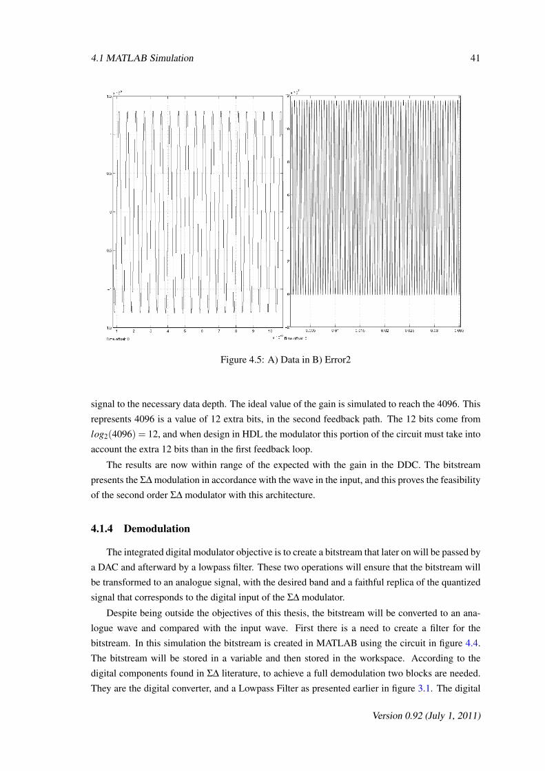
4.1 MATLAB Simulation 41
Figure 4.5: A) Data in B) Error2
signal to the necessary data depth. The ideal value of the gain is simulated to reach the 4096. This
represents 4096 is a value of 12 extra bits, in the second feedback path. The 12 bits come from
log2(4096) = 12, and when design in HDL the modulator this portion of the circuit must take into
account the extra 12 bits than in the first feedback loop.
The results are now within range of the expected with the gain in the DDC. The bitstream
presents the Σ∆ modulation in accordance with the wave in the input, and this proves the feasibility
of the second order Σ∆ modulator with this architecture.
4.1.4 Demodulation
The integrated digital modulator objective is to create a bitstream that later on will be passed by
a DAC and afterward by a lowpass filter. These two operations will ensure that the bitstream will
be transformed to an analogue signal, with the desired band and a faithful replica of the quantized
signal that corresponds to the digital input of the Σ∆ modulator.
Despite being outside the objectives of this thesis, the bitstream will be converted to an ana-
logue wave and compared with the input wave. First there is a need to create a filter for the
bitstream. In this simulation the bitstream is created in MATLAB using the circuit in figure 4.4.
The bitstream will be stored in a variable and then stored in the workspace. According to the
digital components found in Σ∆ literature, to achieve a full demodulation two blocks are needed.
They are the digital converter, and a Lowpass Filter as presented earlier in figure 3.1. The digital
Version 0.92 (July 1, 2011)

42 Digital Σ∆ Modulator
Figure 4.6: C) Acc2 D) Bitstream
converter can be in a simple form to be achieved by filtering the bitstream. So for the demodulation
portion two filters will be used. To create the first filter a function called tukeywin(w,r) was used.
This function creates an array w with he values of the cosine function, and the r is the window
used. To create the second filter the function ones(m,n), where m is the lines of the array and n
is the columns, is sufficient. The bitstream is filtered by being convoluted with the desired filter.
After the result of the convolution is calculated, it was again convoluted by the second filter.
The commands used in the MATLAB function to generate the demodulated wave were the follow-
ing table 4.1.
bitstream;f1= tukeywin(512,1);z1= conv(f1, bitstream);f2= ones(256,1);z2= conv(f2, z1);plot (z2, ’r’);
Table 4.1: MATLAB function for demodulation
Version 0.92 (July 1, 2011)

4.1 MATLAB Simulation 43
Figure 4.7: A) Data in B) Error2
Figure 4.8: C) Acc2 D) Bitstream
Version 0.92 (July 1, 2011)

44 Digital Σ∆ Modulator
The Input quantized wave is presented in the figure 4.9, and the output wave after the convo-
lution is presented in the figure 4.10. Both waves are very identical, but the analogue output wave
has errors generated from the quantization, that can not be removed, despite being very small.
Figure 4.9: Digital Input Wave
Figure 4.10: Analogue Output Wave
Version 0.92 (July 1, 2011)
4.2 HDL Implementation 45
4.1.5 SNR in the Output
One of the main objectives for this modulator is to reach the SNR of 100 dB. Observing the
output wave in the figure 4.10, its clear that is not a perfect sine wave and some error (or noise) is
present. To address this problem it is necessary to accurately measure the SNR. The process used
in subsection 4.2.5, is not feasible in the output for several reasons. The amount of signal is not
known, and the amount of noise is also unknown. From the theoretical studies it was established
that the Σ∆ modulator has a transfer function equal to one for the signal, so one way that could
work is to measure the power of the signal without the quantization noise in the input, measure the
output signal power and theoretically the remaining is the noise. This however is only for ideal
and first order models and not suitable for this case.
Another method of measure the SNR is to actually calculate the output spectrum of the mod-
ulated bitstream after being converted to the analogue wave. The method for measuring the SNR
with the figure 4.11, consists in observing the spectrum. The higher point is the spectrum of the
modulated wave is located in the frequency of the input wave, the rest of the spectrum visible is
the amount of noise. The relation of SNR is given by the level of the signal with the level of the
noise, and because the relation is made in dB, is simply the level of the signal in dB minus the
level of noise in dB. The observation window is for the range until 20000 Hz, any spectrum above
that will be removed by the lowpass filter used in the analogue part of the DAC as shown in figure
3.1.
The figure 4.11, reveals a level of 195.8 dB for the wave at 50 Hz, and the remaining noise
level occurs at 93.4 dB at the maximum and later on is even lower. This means an SNR of over
100 dB ( 195.8−93.4 = 102.4dB), and it is very promising for the HDL implementation.
4.2 HDL Implementation
4.2.1 Proposed Σ∆ Modulator
After all the characteristics were defined for the Σ∆ Modulator, and all the performance were
reached, the next step is the creation and description in HDL of the proposed architecture. The
Σ∆ Modulator circuit was created using Verilog hardware description language. To guarantee that
the implementation complains the previously required and presented functionality, the circuit was
checked through a verification process also developed using Verilog. The verification process con-
sisted in observing the Input, Output, and also the internal working in the data path.
In figure 4.12 is presented the structure for the description created in Verilog. The main blocks
are presented and also the number of bit depth they compute as in calculated in the subsection
4.1.3. The main blocks present the functionality of the each block and the organization and loca-
tion of them represent the data path.
Version 0.92 (July 1, 2011)

46 Digital Σ∆ Modulator
Figure 4.11: Spectrum for the MATLAB simulation
Figure 4.12: Block Diagram for the Code
Version 0.92 (July 1, 2011)

4.2 HDL Implementation 47
Since the Input data has 18 bits, and the calculations are made in 28 bits for the second modu-
lator, the signal must be expanded. After the expansion the signal goes through the first NSL and
then it is expanded to another 28 plus 12 bits as explained in subsection 4.1.3. After expanded
to 40 bits can then enter the second NSL. The reason for using a different bit depth for different
NSL is because in the second NSL there is really a need for 40 bits to prevent overflow but in the
first NSL it is not. Therefore there is no need on increasing the size of the circuit only to make it
equal along the data path. In the previous discussed architectures, to expand the bitstream back to
the original bit depth, there was a DDC to supply both the NSL1 and NSL2. But for this imple-
mentation, the bit depth is different among the NSL 1 and NSL2, therefore two expander are used.
The concept is exactly the same, with the first expander increasing the bit depth to 28 bits, and the
second expander to 40 bits.
4.2.2 Verification Process
Figure 4.13: Verification Process
The figure 4.13, describes how the verification process is organized. This process, performed
by a testbench, can be described into three different steps:
• Stimulation and output data capture;
• Waveform analisys;
• MATLAB calculations;
Version 0.92 (July 1, 2011)

48 Digital Σ∆ Modulator
The verification starts with the stimulation of the Σ∆ Modulator. To stimulate the device under
test (DUT) the testbench reads a file containing data previously created by a waveform generator
(as explained in subsection 4.2.3). This file contains a quantized sine wave, which will alow the
emulation of the interpolation filter output. At the same time the testbench captures the bitstream
output of the implemented second order modulator, and save it to a text file, that will be used for
the MATLAB calculations. One of the characteristics of the developed testbench is that it allows
the user to define the desired OSR by means of interpolating the input data, as many times as
necessary. This interpolation occurs when the testbench send a sample of the data file from the
waveform generator, and the modulator reads it the number of times as the OSR was defined in
the initial parameters of the simulation.
After the simulation ends, the stimulus provided to the DUT and the respective behavior of the
Σ∆ Modulator, as well as its internal activity were observed, using Cadence Simvision software.
This observation provides a initial idea of the DUT functionality, to preliminary confirm the cor-
rect implementation.
Finally, to demonstrate that the second order Σ∆ Modulator, reached the initial objectives de-
fined in chapter 1.2, MATLAB calculations were made. To perform these calculations the text file
generated in the first step will be used. The results from these calculations are presented in the
subsequent sections.
Al these three different steps are needed to guarantee and to prove the correct functioning of
the designed second order Σ∆ Modulator.
4.2.3 Data Path
With the results obtained in the simulations in subsection 3.2.2, and in subsection 4.1.4, there
are some results that can be expected even for a second order modulator. The bitstream in the
output must be also reconstructed to confirm that the bitstream represents the wave in the output.
In this simulation, a input wave is first generated with a small program that creates a sine
wave. This program was supplied by Silicongate and the output is a text file with the 18 bits
representation of each sample. In table 4.2 the parameters of the wave are presented, this is
important to establish the input wave characteristics. The analogue representation of the output
wave is presented in the figure 4.14.
For the first simulations the most important parameters observed were, the Input and the bit-
stream in the Output. Other points in the data path observed were the Error1, the Acc1, the Error2,
and the Acc2. The Error is the difference between the value to be compared, Acc is the accumu-
lation of the Error, and the number 1 or 2 is the location in the first or second NSL respectively.
Version 0.92 (July 1, 2011)

4.2 HDL Implementation 49
Wave sineSignal signed
Number of Samples 128Gain 1
Periods 10Output File txt file
Table 4.2: Input Wave Characteristics
Figure 4.14: Generated Sine Wave
These observations permitted to verify any inconsistency with the predicted results and with the al-
ready observed waves in the figure 3.5, and therefore verify the functionality. The points observed
are presented in the figure 4.15.
Figure 4.15: A)Input B)Error1 C)Acc1 D)Error2 E)bitstream
The results presented in the figure 4.15 are very promising. The both the Errors present the
difference between the output and the input and the Accumulators also accumulate the Errors.
Version 0.92 (July 1, 2011)

50 Digital Σ∆ Modulator
More importantly the bitstream in the output represents the expected behavior for representing a
sine wave. In the positive swing of the signal the bitstream is mostly ones, and as it is decreasing
to the negative swing the number of zeros become more frequent and in the lowest input level the
bitstream is mostly zeros.
4.2.4 Wave Reconstruction
One important aspect that was already addressed in the MATLAB simulations, is that a simple
observation of the bitstream is somewhat indicative of the correct functioning, but is not a guar-
antee that the wave is correctly represented. To verify and observe the bitstream and its correct
representation, the already mentioned verification process created in Verilog, permits to extract to
a file the binary representation of the bitstream. After that a repetition of the process used for the
MATLAB simulations is used to represent the analogue wave. The output reconstructed wave is
presented in the figure 4.16.
Figure 4.16: Reconstructed Sine Wave
The reconstruction of the wave reveals a sine wave just like the input wave for the circuit.
This may be a good indication of the correct modulation, and indeed looks promising, but the
most important aspect of the SNR cannot be attained just by observing the waves. The necessary
calculations for the SNR and the correct functioning of the Σ∆ Modulator will be presented in the
subsection 4.2.6.
Version 0.92 (July 1, 2011)

4.2 HDL Implementation 51
4.2.5 SNR in the Input
To measure the SNR in the Input, The same process used in the subsection 4.2.5, is not cor-
rect. Now the input wave is generated already quantized and therefor is not possible to have the
original wave without the quantization error. To calculate the SNR now, there must be used the
equations defined in the State of the Art in chapter 2. The equations used is the 2.11 that relates
the amplitude of a sine wave with the noise level, and the equation 2.4, that relates the noise level
with the quantization bits.
Generating a wave with and amplitude of 131070, corresponding to the maximum input that
the supplied generator can create, and using 18 bits, which corresponds to a number of quantization
intervals of 218 = 262144 the equation remains as shown in 4.3.
SNR =12×1310702
2×∆2 (4.3)
∆2 =
1310702
2621442 (4.4)
Replacing the values in each equation now remains the equation 4.5
SNR =12×2621442
2= 1.3744×10¹¹ (4.5)
And in dB the final SNR will be given by equation 4.6. And is very close for the expected
value of SNR for the error induced by the quantization with 18 bits of a sine wave.
SNR = 10× log10(1.3744×10¹¹) = 111.38dB (4.6)
4.2.6 SNR in the Output
As the output bitstream is reconstructed and the wave is in analogue form, now the SNR
can be measured. This value is very important to establish the performance of the proposed Σ∆
Modulator. The bitstream is stored in a text file and is then exported to the MATLAB environment
for the calculations. The figure 4.17, presents the spectrum for the reconstructed output wave.
The method for measuring the SNR with the figure 4.17, consists observing the spectrum. The
same method as applied in the subsection 4.1.5 will be used.
Version 0.92 (July 1, 2011)
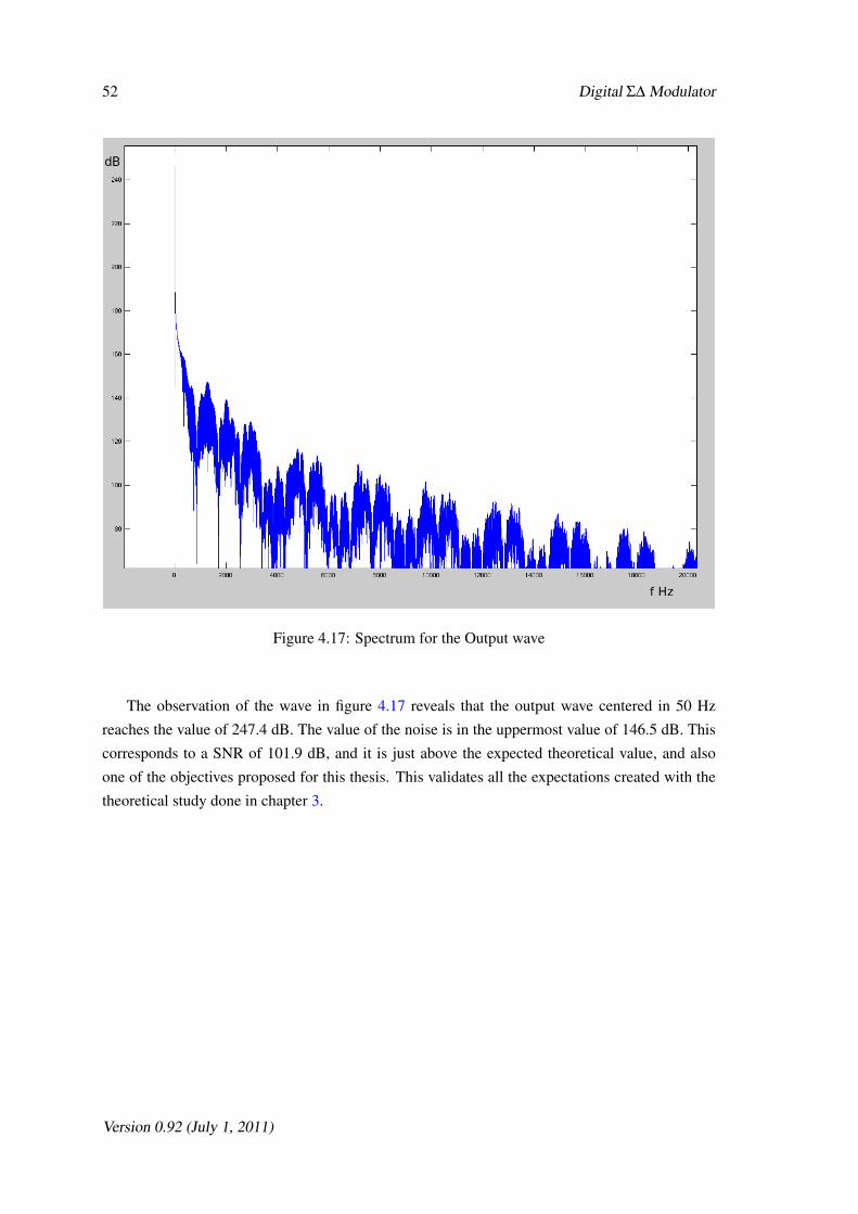
52 Digital Σ∆ Modulator
Figure 4.17: Spectrum for the Output wave
The observation of the wave in figure 4.17 reveals that the output wave centered in 50 Hz
reaches the value of 247.4 dB. The value of the noise is in the uppermost value of 146.5 dB. This
corresponds to a SNR of 101.9 dB, and it is just above the expected theoretical value, and also
one of the objectives proposed for this thesis. This validates all the expectations created with the
theoretical study done in chapter 3.
Version 0.92 (July 1, 2011)

Chapter 5
Conclusions
In this section, the conclusions for the implementation of the Σ∆ Modulator will be presented.
The methods for the design and simulation for the Σ∆ are somewhat complex, and achieving
certain results is dependent of a very wide range of factors. this chapter will present the most
important conclusions in that regard. Next the future work down the road is presented, and finally
a very concise consideration about this thesis and the solution presented.
5.1 Conclusions
The Σ∆ Modulator is a very effective way to create a oversampled converter, in this case a
DAC.
The comprehension of the theoretical aspects are complex and demands a good knowledge of
signal processing and audio implementations. The application of the theoretical models requires
capabilities in software simulations, and more importantly of the HDL implementation of the de-
sired models.
The HDL permited to easily and in a natural way to analyse the response and behavior of each
bulding block of the modulator. The correction of the number of bit depth was also a simple task
with HDL implementation, this permited to change the given number of input bits and with the
method presented a great modularity can be achieved.
During the early stages of this thesis, care was taken not to choose over complex models for
the solution. This proposed solution was made with a potential commercial objective in mind and
that fact steers for a more straightforward solution that sometimes is less relevant in a purely aca-
demic thesis. Despite being a simple architectural solution, it was proven that great performance
can be achieved with little changes in the OSR for example (see 3.1.3).
53

54 Conclusions
The MATLAB simulation were very cumbersome to realize, and many times specific aspects
of the simulations where staled because of the internal working in the MATLAB. Still this proved
to be a very important tool in designing the proposed architecture and in validating the respective
results. The MATLAB allied with the Simulink environment and the Fdatool where irreplaceable
for this study. It was proven that many stages of the design can be detailed and upgraded.
Because the audio prospective of this thesis, filtering was also a very important aspect for this
modulator. The Interpolation Filter developed, and in particular the method realized, permitted in
greatly reducing the size of the IF, and also the power consumption (see subsection 3.6). Once
again the Fdatool was very valuable.
For the HDL implementation, the Verilog description language proved to be an ideal choice
because of the ease in which the small processing blocks can be individually created, simulated,
and verified. The complement of the Ncsim and the Simvision was also very important to the
implementation and concatenation of the smaller blocks into forming the proposed architecture
for the second order Σ∆ Modulator 4.2.
As far as performance goes, the proposed modulator achieved the required objectives, and a
simple methods to increase the performance was also demonstrated. These methods can be simple
in the implementation but have great overall implications.
5.1.1 Incomplete Work
Several objectives were stated in the early pages of this dissertation. Despite the most impor-
tant one was achieved, the implementation of a 100 dB digital Σ∆ Modulator, some other were
not fully completed at the writing of this thesis. The comparative study among two or three dif-
ferent Σ∆ architectures was one of them. The reason is mainly because in terms of architecture
simplicity the second order modulator is the more attractive, the first order should be the best, but
is unreachable to 100 dB in SNR for the commercially used OSR. Despite the second order being
the most simple, with the implementation with a given fabrication technology this paradigm can
change because now a higher order Σ∆ must need a lower OSR, and that reflects in the total area
for the interpolation filter. It can be an advantage to go to higher orders, and without the compar-
ative study is not possible to verify or deny it.
Many times different work paths where choosen that proved to be not the correct one. For
example, the cascading of the interpolation filter in section 3.3.4, greatly reduced the avaiable
time. At first a generic algorith was tried to implement the cascading components with the correct
order. Only after several atempts a simplier and intuitive method was developed to achieve the
same functionality results. Another example of a wrong path was the implementation of the HDL
module. The dynamic parameters calculated in 4.1.3, became an imperative after several failed
simulations. The avaiable Σ∆ literature did not addressed this problem and did not presented hints
Version 0.92 (July 1, 2011)

5.2 Future Work 55
for its solving.
For the completion of the dissertation, many and varied subjects were integrated to achieve a
final solution. This presented a great challenge and was a great motivation for the choice of this
dissertation, but was also a pivotal point in undermine the work developed and presented this far.
This however will not have repercussions in the future work presented in subsection 5.2
5.2 Future Work
For this solution to be a final commercial product many steps are still needed. The most
important and more relevant are as follow:
A implementation and synthesis of the proposed architecture must be done in a specific CMOS
tech. Then several techs must be also synthesized with the proposed solution. Because certain
techs can be more optimized in terms of area or power consumption, a choice for a certain avail-
able tech can render certain previous choices undesirable. For example, lets consider the 350 nm
versus the 90 nm. The proposed architecture works with an OSR of 128, but with an certain area
developed. If the 350 nm can consume an amount of power for the necessary area, the 90 nm can
consume a lot less and require less area. This study of area versus consumption is very important,
specially for a commercially aimed solution.
A comprehensive study with several sources in the input. All the simulation were made with
specifics frequencies at very fixed levels, ranging from the 20 Hz to 20000 Hz. In reality a small
audio track for example may store more than one frequency, at different levels and with the noise
dispersed.
A processing chain in which a small sound is recorded, the recorded sound is played and then
is quantized to 18 bits and driven into the Σ∆ Modulator. Despite being outside the scope of this
thesis, after the bitstream from the modulator is captured, it will be passed through a demodulator
and converted to an analogue form. The objective will be to listen the recorded sound in the end
but without some of the noise that will be recorded and created during the quantization.
The implementation of the architecture can also be made in a FPGA, and the results driven
back to the computer to be demodulated or even use a small demodulator that transforms the sig-
nal back into analogue. The next logical step and probably the most complicated one, would be
a physical implementation of the circuit in the technology decided previously. Then all the sim-
ulations could also be made again but in a real circuit just like it would be in a commercial product.
Version 0.92 (July 1, 2011)

56 Conclusions
5.3 Final Considerations
The proposed solution presented in this thesis is still in a very distant state from becoming
a commercial product. Still the fundamentals and the solutions shown where, demonstrate the
feasibility, in creating a simple and reliable Σ∆ Modulator, for audio applications with very good
performance characteristics.
Version 0.92 (July 1, 2011)

References
[1] RC Cofer and Ben Harding. Fixed point dsp and algorithm implementation. EETIMESwebsite, october 2005.
[2] José M. de la Rosa. Sigma-Delta Modulators: tutorial overview, design guide, and State ofthe Art survey. IEEE Transactions on circuits and systems, 58(1), January 2011.
[3] James M. Bryant. How a Σ∆ ADC Works. June 2006.
[4] Uwe Beis. An introduction to delta sigma converters, june 2008.
[5] Steven Norsworthy, Richard Schreier, and Gabor Temes. Delta Sigma Data Converters,theory, design and simulation. IEEE Press, 1 edition, 1997.
[6] Richard Schreier and Gabor Temes. Understanding Delta-Sigma Data Converters. Wiley-IEEE Press, 1 edition, 2004.
[7] F. Maloberti. A low power sinc3 filter for Σ∆ modulators. In Proceedings ISCAS, May 2007.
[8] John Watkinson. The Art of Digital Audio. Focal Press, 1 edition, 1994.
[9] David Jarman. A Brief Introduction to Sigma Delta Conversion. May 1995.
[10] W. L. Lee and C. G. Sodini. A topology for higher order interpolative coders. IEEE Int.Symp. Circuits Press, 1987.
[11] Richard Schreier. Stability Theory for delta-sigma Data Converters. Wiley-IEEE Press,1997.
[12] Wu-Chun Feng. Making a case for efficient Supercomputing. ACM Queue, October 2003.
[13] Y. Chae & G. Han. Low voltage, low power, inverter-based switched-capacitor Σ∆ modula-tor. IEEE J. Solid-State Circuits, 44:369–373, May 2009.
[14] M. C. Huang & S. I. Lu. A fully differential comparator-based switched-capacitor Σ∆ mod-ulator. IEEE J. Solid-State Circuits, 44:369–373, May 2009.
[15] J. Sauerbrey et al. A 0.7-V MOSFET-only switched-opamp Σ∆ modulator in standard digitalCMOS technology. IEEE J. Solid-State Circuits, 37:1662–1669, December 2002.
[16] F. Chen et al. A 1.5 V 1 mA 80 dB passive Σ∆ ADC in 0.13 µm digital CMOS process. IEEEISSCC Dig. Tech. Papers, 54 - 55:244–245, February 2003.
[17] J. Roh et al. A 0.9-V 60 µW 1-bit fourth order Delta Sigma modulator with 83 dB dynamicrange. IEEE J. Solid-State Circuits, 43:361–370, February 2008.
57

58 REFERENCES
[18] L. Yao et al. A 1-V 140 µW 88 dB audio Sigma Delta modulator in 90 nm CMOS. IEEE J.Solid-State Circuits, 39:1809–1818, November 2004.
[19] Ams cmos technology overview.
[20] Tsmc 0.18 um technology overview (mpw).
[21] Umc 0.13 um technology overview (mpw).
[22] Umc 90nm technology overview (mpw).
[23] Steven W. Smith. The Scientist and Engineers Guide to Digital Signal Processing. CaliforniaTechnical Publishing, 2 edition, 1997.
[24] Noura Ben Ameur. Design of efficeint digital interpolation filters and sigma-delta modulatordor audio dac. In International Conference on Design and Technology of Integrated Systemsin Nanoscale Era. IEEE, 2008.
[25] Glenn Elert. Frequency range of human hearing, 2004.
[26] A. Mukhtar, H. Jamal, and U. Farooq. An area efficient interpolation filter for digital audioapplications. IEEE Transactions on Consumer Electronics, 55, may 2009.
[27] Ivan W. Selesnick and C. Sidney Burrus. Exchange algorithms that complement the parks-mcclellan algorithm for linear-phase fir filter design. IEEE Transactions on Circuits andSystems, 44, february 1997.
Version 0.92 (July 1, 2011)