digital circuits - neff · digital circuits networks and embedded software digital circuits by...
TRANSCRIPT

Digital Circuits
Networks and Embedded Software Digital Circuits by Wolfgang Neff

Introduction (1)
• Topic
– Analysis of digital circuits
– Synthesis of digital circuits
• Bases on Boolean algebra
– Logical operators are represented by symbols
– Logical values are represented voltages
• Positive logic: 0 → Low voltage, 1 → High voltage
• Negative logic: 0 → High voltage, 1 → Low voltage
28.04.2016 Digital Circuits, © W. Neff 2

Introduction (2)
• High and low is produced by switches
28.04.2016 Digital Circuits, © W. Neff 3
Part of interest

Introduction (3)
• Combination of switches realize AND and OR
28.04.2016 Digital Circuits, © W. Neff 4
A B A∧B
0 0 0
0 1 0
1 0 0
1 1 1
A B A∨B
0 0 0
0 1 1
1 0 1
1 1 1

Introduction (4)
• Digital circuits use transistors as switches
28.04.2016 Digital Circuits, © W. Neff 5

Introduction (5)
• There are many types of transistors
NPN / N-Channel PNP / P-Channel
Basis
Collector
Emitter
Gate
Drain
Source
Basis
Collector
Emitter
Gate
Drain
Source
bipolar
MOSFET
28.04.2016 Digital Circuits, © W. Neff 6

Graphical Symbols (1)
• Buffer
• Negation (NOT, ¬)
1 a y
European Style (IEC 60617-12)
American Style (Mil-STD-806)
1 a y
Inversion Circle
a y=a
0 0
1 1
a y=¬a
0 1
1 0
28.04.2016 Digital Circuits, © W. Neff 7

Graphical Symbols (2)
• Disjunction (OR, )
• Conjunction (AND, )
≥1 a
b y
& a
b y
a b y=a∨b
0 0 0
0 1 1
1 0 1
1 1 1
a b y=a∧b
0 0 0
0 1 0
1 0 0
1 1 1
28.04.2016 Digital Circuits, © W. Neff 8

Graphical Symbols (3)
• NOR (⊽)
• NAND (⊼)
a b y=a⊽b
0 0 1
0 1 0
1 0 0
1 1 0
a b y=a⊼b
0 0 1
0 1 1
1 0 1
1 1 0
≥1 a
b y
& a
b y
28.04.2016 Digital Circuits, © W. Neff 9

Graphical Symbols (4)
• Compound AND-Gate
– y = a0 ∧ a1 ∧ a2 … = 𝑎𝑖𝑛𝑖=0
–
• Compound OR-Gate
– y = a0 ∨ a1 ∨ a2 … = 𝑎𝑖𝑛𝑖=0
–
&
a0
a1
y
an
…
≥1
a0
a1
y
an
…
else 0
1each if 1),,( 10
iaaa
else 1
0each if 0),,( 10
iaaa
28.04.2016 Digital Circuits, © W. Neff 10

Logic Gates
• Families of logic gates
Family TTL
MOS
PMOS
NMOS
CMOS
28.04.2016 Digital Circuits, © W. Neff 11

TTL (1)
• Transistor-Transistor-Logic
– TTL circuits operate with a 5 V power supply.
– H and L are defined for voltage regions.
– Input and output ranges differ.
TTL Signal Input Output
L 0 V … 0,8 V 0 V … 0,4 V
H 2 V … 5 V 2,4 V … 5 V
28.04.2016 Digital Circuits, © W. Neff 12

TTL (2)
• Signal levels
0
1
3
5
2
4
Vo
ltag
e U
/ V
< 0,8 V: L
> 2 V: H-Signal
< 0,4 V: L
> 2,4 V: H-Signal
TTL-Gate
Signal distance
28.04.2016 Digital Circuits, © W. Neff 13

TTL (3)
• Fundamental TTL NAND gate
x
y
z
VCC (Voltage of the common collector )
GND
A B A⊼B
0 0 1
0 1 1
1 0 1
1 1 0
28.04.2016 Digital Circuits, © W. Neff 14

TTL (4)
• TTL gates are found in the IC 7400 series.
IC Gate Number Lines IC Gate Number Lines
7408 AND 4 2 7400 NAND 4 2
7411 AND 3 3 7410 NAND 3 3
7421 AND 2 4 7420 NAND 2 4
7432 OR 4 2 7402 NOR 4 2
7404 NOT 6 1 7427 NOR 3 3
28.04.2016 Digital Circuits, © W. Neff 15

TTL (5)
• Device description
– 7411: Triple 3-Input Positive-AND Gates (about 0,30 €)
&
&
&
1A
1B
2A
2B
2C
2Y
5V
1C
1Y
3C
3B
3A
3Y
1A 1B 2A 2B 2C 2Y
GND
74
11
1C 1Y 3C
VCC
3B 3A 3Y
Mark
28.04.2016 Digital Circuits, © W. Neff 16

CMOS (1)
• Signal levels (4000 series CMOS Logic ICs)
0
1
3
5
2
4
Vo
ltag
e U
/ V
< 1,5 V: L
> 3,5 V: H-Signal
< 0,05 V: L
> 4,95 V: H
CMOS-Gate
Signal distance
28.04.2016 Digital Circuits, © W. Neff 17

CMOS (2)
• Switching with MOSFETs
N-Channel P-Channel
L H L H
28.04.2016 Digital Circuits, © W. Neff 18
off on on off

CMOS (3)
• Fundamental CMOS gates
NOT-Gate NAND-Gate
VDD
GND
a
a
b
b y a
a
y
VDD
GND
28.04.2016 Digital Circuits, © W. Neff 19

CMOS (4)
• CMOS gates are found in the IC 4000 series
– There are also CMOS version of the TTL gates
• 74HC00: CMOS compatible voltage levels
• 74HCT00: TTL compatible voltage levels
IC Gate Number Lines IC Gate Number Lines
4081 AND 4 2 4011 NAND 4 2
4073 AND 3 3 4023 NAND 3 3
4082 AND 2 4 4012 NAND 2 4
4071 OR 4 2 4001 NOR 4 2
4049 NOT 6 1 4025 NOR 3 3
28.04.2016 Digital Circuits, © W. Neff 20

Analysis
• Find the switching function of a given circuit
– Solution: ¬(¬((a∧¬b)∨b)∨(¬a∧¬c))
a b c
&
&
≥1
≥1
28.04.2016 Digital Circuits, © W. Neff 21

Design (1)
• Find a digital circuit for a given problem
– Please add two bits. If you add two numbers a carry can occur. You need not only determine the result but also the carry. On the other hand there can already be a carry when you add two numbers. You have to handle this carry, too. This type of circuit is called full adder. • Mathematical description of a full adder
– {0,1}×{0,1}×{0,1} ⟼ {0,1}2 (a,b,ci) ⟶ (co,a+b) ci: carry in; co: carry out
28.04.2016 Digital Circuits, © W. Neff 22

Design (2)
• Example
Bit position 3 2 1 0
1st Number (7) 0 1 1 1
2nd Number (5) 0 1 0 1
Carry 1 1 1 0
Result (12) 1 1 0 0
28.04.2016 Digital Circuits, © W. Neff 23

Design (3)
• Truth table of a one bit full adder
a b ci co y
0 0 0 0 0
0 0 1 0 1
0 1 0 0 1
0 1 1 1 0
1 0 0 0 1
1 0 1 1 0
1 1 0 1 0
1 1 1 1 1
28.04.2016 Digital Circuits, © W. Neff 24
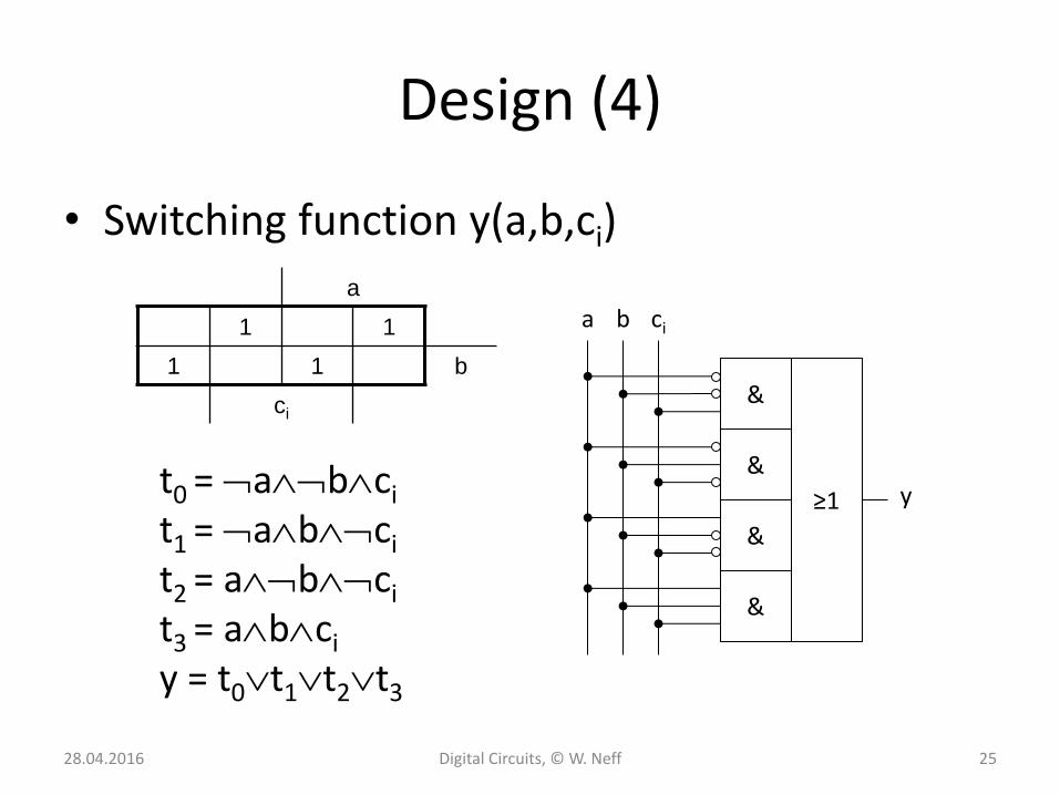
Design (4)
• Switching function y(a,b,ci)
≥1
&
a b ci
&
&
&
y
a
1 1
1 1 b
ci
t0 = abci
t1 = abci t2 = abci t3 = abci y = t0t1t2t3
28.04.2016 Digital Circuits, © W. Neff 25

Design (5)
• Switching function co(a,b,ci)
≥1
&
&
&
a b ci
co
a
1
1 1 1 b
ci
t0 = aci
t1 = bci t2 = ab co = t0t1t2
28.04.2016 Digital Circuits, © W. Neff 26
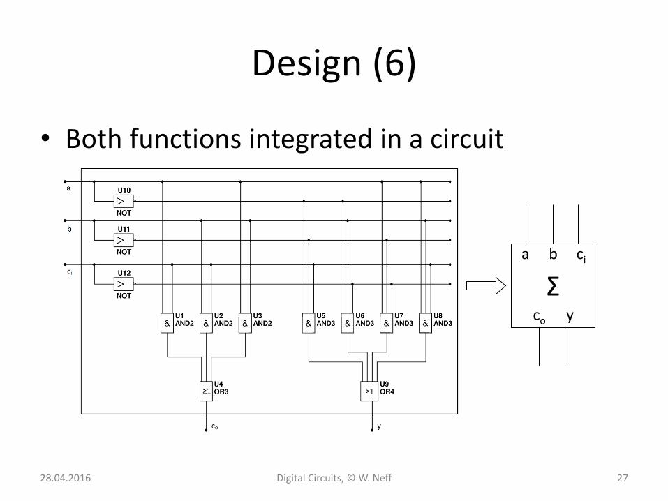
Design (6)
• Both functions integrated in a circuit
Σ a b ci
y co
28.04.2016 Digital Circuits, © W. Neff 27

Design (7)
• Combined one bit full adders
a0 b0 c0
y0
a1 b1 c1
y1
a2 b2 c2
y2
a3 b3 c3
y3 c
first carry in is always 0
ripple carry
Σ a b ci
y co
Σ a b ci
y co
Σ a b ci
y co
Σ a b ci
y co
28.04.2016 Digital Circuits, © W. Neff 28

Design (8)
• Integrated four bit half adder
Σ a1 a0 a3 a2 b3 b2 b1 b0
y2 y3 y0 y1 c
c
Σ
a b
y
4 4
1 4
Σ a b
y co
28.04.2016 Digital Circuits, © W. Neff 29

Latches (1)
• Implementation of a SR latch
– Bases on two NOR gates with feedback
≥1
≥1
a
b y2
+
y1+
y2
y1
28.04.2016 Digital Circuits, © W. Neff 30

Latches (2)
• Truth table of a SR latch
a b y1 y2 y1+ y2
+
0 0 0 0 1 1
0 0 0 1 0 1
0 0 1 0 1 0
0 0 1 1 0 0
0 1 0 0 1 0
0 1 0 1 0 0
0 1 1 0 1 0
0 1 1 1 0 0
continues on the next table
a b y1 y2 y1+ y2
+
1 0 0 0 0 1
1 0 0 1 0 1
1 0 1 0 0 0
1 0 1 1 0 0
1 1 0 0 0 0
1 1 0 1 0 0
1 1 1 0 0 0
1 1 1 1 0 0
insta
ble
28.04.2016 Digital Circuits, © W. Neff 31

Latches (3)
• Characteristics of a stable SR latch
– a=0, b=0 (R=0, S=0, Q+=Q)
stable only if y1 ≠ y2 or y1 = y2 (we call y1 Q from now on)
– a=0, b=1 (R=0, S=1, Q+=1)
always stable and y1 = 1 (we call b Set from now on)
– a=1, b=0 (R=1, S=0 , Q+=0)
always stable and y1 = 0 (we call a Reset from now on)
– a=1, b=1 (R=1, S=1 , Q+=undefined)
invalid since it violates y1 ≠ y2
28.04.2016 Digital Circuits, © W. Neff 32

Latches (4)
• Symbol, state table and state diagram
S
R Q
Q=0 Q=1
R=0; S=X R=X; S=0
R=1; S=0
R=0; S=1
S R Q+ Action
0 0 Q Store
0 1 0 Reset
1 0 1 Set
1 1 X Invalid
28.04.2016 Digital Circuits, © W. Neff 33

Latches (5)
• Synchronous SR latch
– C=0: R und S may change, Q is stable
– C=1: R und S must be stable, Q may change
S
R
Q
Q
&
&
C S
R
28.04.2016 Digital Circuits, © W. Neff 34

Latches (6)
• Symbol and state table of a sync SR latch
C S R Q+ Action
0 X X Q Store
1 0 0 Q Store
1 0 1 0 Reset
1 1 0 1 Set
1 1 1 X Invalid
1R C1 1S
R C S
Q
Q
28.04.2016 Digital Circuits, © W. Neff 35

Latches (7)
• Time diagram of a synchronous SR latch
28.04.2016 Digital Circuits, © W. Neff 36

Triggers (1)
• Active and passive state
– Active state Output depends on input
– Passive state Input has no effect on output
– Example: synchronous SR latch
• C=1: active state
• C=0: passive state
28.04.2016 Digital Circuits, © W. Neff 37

Triggers (2)
• Synchronization
– Level triggers The active state depends on the level of the trigger signal: 0 or 1
– Edge triggers The active state depends on the level change of the trigger signal: 0→1 or 1→0
28.04.2016 Digital Circuits, © W. Neff 38

Triggers (3)
• Graphical symbols of triggers
1R C1 1S
1R C1 1S
1R C1 1S
Active Level is C=1
Active Level is C=0
Active Edge is C=0→1
Active Edge is C=1→0 1R C1 1S
28.04.2016 Digital Circuits, © W. Neff 39

Triggers (4)
• Time diagram of a edge triggered SR latch
28.04.2016 Digital Circuits, © W. Neff 40

Flip-flops
• The JK flip-flop has no invalid state
• The D flip-flop is used to store data
1J C1 1K
J K Q+ Action
0 0 Q Store
0 1 0 Reset
1 0 1 Set
1 1 ¬Q Toggle
1D
C1
D Q+ Action
0 0 Reset
1 1 Set
28.04.2016 Digital Circuits, © W. Neff 41

Combinational Circuits
• Output depends on current input only
– History is of no importance
– The system has no memory
Combinational Circuit
y=f(x)
x y
28.04.2016 Digital Circuits, © W. Neff 42

Sequential Circuits (1)
• Output depends on previous inputs
– History is important
– The system has a memory
Sequential Circuit
y(tn)=f(x(tn),x(tn-1),…)
x(t) y(t)
Clock
28.04.2016 Digital Circuits, © W. Neff 43

Sequential Circuits (2)
• Sequential Circuits are finite state machines (FSM)
• Two types are frequently used
– Mealy Machine (dashed arrow allowed)
– Moore Machine (dashed arrow not allowed)
28.04.2016 Digital Circuits, © W. Neff 44

Sequential Circuits (3)
• They are finite state machines
• Final state machines have
– A set of states S
– An initial state s0
– A set of final states
– Transitions
28.04.2016 Digital Circuits, © W. Neff 45

Sequential Circuits (4)
• Example
– Has a bit sequence an even number of 1?
• States: even, odd
• Initial state: even
• Final state: none
• Transitions: Q a Q+
even 0 even
even 1 odd
odd 0 odd
odd 1 even
28.04.2016 Digital Circuits, © W. Neff 46

Sequential Circuits (5)
• State diagram of the FSM
start state states
transition
input
start state
28.04.2016 Digital Circuits, © W. Neff 47
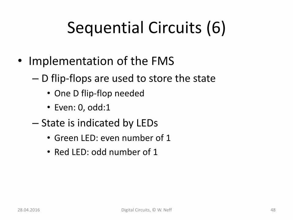
Sequential Circuits (6)
• Implementation of the FMS
– D flip-flops are used to store the state
• One D flip-flop needed
• Even: 0, odd:1
– State is indicated by LEDs
• Green LED: even number of 1
• Red LED: odd number of 1
28.04.2016 Digital Circuits, © W. Neff 48

Sequential Circuits (7)
• Control logic
– Input: external input & internal state
– Output: new state stored by flip-flop
– Information provided by transition table
Q a Q+
0 0 0
0 1 1
1 0 1
1 1 0
𝑄+ = ¬𝑄 ∧ 𝑎 ∨ 𝑄 ∧ ¬𝑎
28.04.2016 Digital Circuits, © W. Neff 49

Sequential Circuits (8)
• Output logic
– Input: state
– Output: signal for green and red LED
– The FSM is a Moore machine
Q g(Q) r(Q)
0 1 0
1 0 1
𝑔 𝑠 = ¬𝑄
𝑟 𝑠 = 𝑄
28.04.2016 Digital Circuits, © W. Neff 50

Sequential Circuits (9)
• Solution
28.04.2016 Digital Circuits, © W. Neff 51

Important Expressions (1)
• digital circuit
• analogue
• digital
• continuous
• discrete
• digital logic
• switch
• switching function
• Digitalschaltung
• analog
• digital
• kontinuierlich
• diskret
• Schaltlogik
• Schalter
• Schaltfunktion
28.04.2016 Digital Circuits, © W. Neff 52

Important Expressions (2)
• pulse train
• square pulse
• pulse diagram
• graphical symbol
• gate
• integrated circuit
• analysis
• design
• Impulsfolge
• Rechteckimpuls
• Impulsdiagramm
• Schaltzeichen
• Gatter
• integrierte Schaltung
• Analyse
• Entwurf
28.04.2016 Digital Circuits, © W. Neff 53

Important Expressions (3)
• adder
• multiplexer
• ALU
• machine code
• flip-flop
• feedback
• state table
• state diagram
• Addierer
• Multiplexer
• ALU
• Maschinencode
• Flipflop
• Rückkopplung
• Zustandsfolgetabelle
• Zustandsdiagramm
28.04.2016 Digital Circuits, © W. Neff 54