devices and chemical sensing applications of metal oxide ...€¦ · devices and chemical sensing...
TRANSCRIPT

APPLICATION www.rsc.org/materials | Journal of Materials Chemistry
Devices and chemical sensing applications of metal oxide nanowires†
Guozhen Shen,* Po-Chiang Chen, Koungmin Ryu and Chongwu Zhou*
Received 22nd September 2008, Accepted 21st October 2008
First published as an Advance Article on the web 20th November 2008
DOI: 10.1039/b816543b
Metal oxide nanowires, with special physical properties, are ideal building blocks for a wide range of
nanoscale electronics, optoelectronics, and chemical sensing devices. This article will describe the state-
of-the-art research activities in metal oxide nanowire applications. This paper consists of three main
sections categorized by metal oxide nanowire synthesis, electronic and optoelectronic devices
applications, and chemical sensing applications. Finally, we will conclude this review with some
perspectives and outlook on the future developments in the metal oxide nanowire research area.
1. Introduction
Due to their special shapes, compositions, chemical and physical
properties, one-dimensional (1-D) metal oxide nanostructures
are the focus of current research efforts in nanotechnology since
they are the commonest minerals in the earth. 1-D metal oxide
nanostructures have now been widely used in many areas, such as
ceramics, catalysis, sensors, transparent conductive films, elec-
tro-optical and electro-chromic devices.1–5 Intensive studies have
been carried out on the synthesis of metal oxide nanowires as well
as the exploration of their novel properties. For example, 1-D
ZnO nanostructures with many different shapes, such as nano-
wires, nanobelts, nanotubes, nanorings, and nanosprings, have
been prepared using many synthesis methods. High-performance
chemical sensors have been fabricated on SnO2, ZnO, and In2O3
nanowires due to their large surface area to volume ratio.
Dr Guozhen Shen
Dr Guozhen Shen received his
Ph.D. degree in Chemistry from
University of Science and Tech-
nology of China in 2003. He
conducted his postdoctoral
research at Hanyang University,
Korea in 2004 and then joined
National Institute for Materials
Science, Japan as a visiting
researcher. Currently, he is
a research scientist in University
of Southern California. He is the
author or co-author of more
than 100 research articles and 5
book chapters. His most recent
research interests include the synthesis and characterization of one-
dimensional nanostructures and their device applications in elec-
tronics and optoelectronics.
Department of Electrical Engineering, University of Southern California,Los Angeles, CA 90089, USA. E-mail: [email protected]; [email protected]; [email protected]; Fax: +1 213 821 4208; Tel: +1 213 821 4208
† This paper is part of a Journal of Materials Chemistry theme issue onNanotubes and Nanowires. Guest editor: Z. L. Wang.
828 | J. Mater. Chem., 2009, 19, 828–839
This article will provide a comprehensive review of the state-
of-the-art research activities focused on devices and chemical
sensing applications of metal oxide nanowires, and can be
divided into three main sections. The first section briefly intro-
duces two synthesis strategies, which include top-down
approaches and bottom-up approaches, with the focus on
bottom-up approaches, for the synthesis of metal oxide nano-
wires. Next, some important electronic and optoelectronic
devices built on metal oxide nanowires are presented, which
include field-effect transistors (FETs), transparent electronics,
lasers and waveguide, nanogenerators, solar cells and photo-
catalysts, and field nanoemitters. In the third part, we will discuss
recent developments in the chemical sensing area of metal oxide
nanowires. The review will then conclude with some perspectives
and outlook on the future developments in the metal oxide
nanowire research area.
2. Synthesis of metal oxide nanowires
Till now, many methods have been developed to synthesize 1-D
metal oxide nanostructures. Basically, they can be described as
two different types: the ‘‘top-down’’ approaches and the
‘‘bottom-up’’ approaches. In this section, we will briefly discuss
Po-Chiang Chen
Po-Chiang Chen holds a B.S.
degree in Physics and a M.S. in
Optoelectronics. He is currently
working toward a Ph.D. degree
in Chemical Engineering and
Materials Science at the
University of Southern Cal-
ifornia. His research focus is on
the device applications based on
1-D nanomaterials, including
chemical sensors, transparent
electronics, and energy conver-
sion and storage devices.
This journal is ª The Royal Society of Chemistry 2009

these two approaches developed to synthesize metal oxide
nanowires.
2.1. Top-down synthesis
‘‘Top-down’’ approaches usually utilize planar, lithographic
techniques to transfer a pre-designed pattern to a substrate which
can form complex high density structures in well-defined posi-
tions on substrates.6,7 For example, Im et al.6 synthesized ZnO
nanowires using a complicated nanoscale spacer lithography
method, which can be used to detect H2 and CO gases. Top-down
approaches have been widely used in the current microelectronic
industry. They can produce nanostructures with very uniform
shapes and electronic properties. However, as the microelec-
tronic industry advances towards ever smaller devices, top-down
approaches will soon reach their physical and economic limits,
which motivates global efforts to search for new strategies to
meet the expected demand for increased computational power as
well as for integrating low-cost and flexible computing in
unconventional environments in the future.
2.2. Bottom-up synthesis
The bottom-up approaches, in which functional electronic struc-
tures are assembled from chemically synthesized nanoscale
building blocks, represent flexible alternatives to conventional
top-down methods. They can go far beyond the limits of top-down
technology in terms of future physical and economic limits.8,9
Table 1 lists a host of 1-D metal oxide nanostructures grown from
bottom-up approaches using different techniques.10–103
To get 1-D metal oxide nanostructures using the bottom-up
approaches, one key concept is to break the growth symmetry of
materials. A straightforward method to break the symmetry for
1-D growth is the use of ‘‘hard’’ or ‘‘soft’’ templates, which may
include the edges of surface steps, carbon nanotubes, porous
membranes, surfactant, or microemulsions. This method is
conceptually very simple and has been widely used to prepare
a variety of metal oxide nanowires. Despite its simplicity, the
Koungmin Ryu
Koungmin Ryu holds a B.S
degree in Metallurgy and a M.S
degree in Materials Science and
Engineering. He is currently
a Ph.D. student at the Univer-
sity of Southern California. His
research interest covers carbon
nanotube synthesis and applica-
tions such as nanotube circuits,
chemical sensing, and OLED
fabricated by carbon nanotube
conductive films. He has pub-
lished 3 journal papers related to
carbon nanotube synthesis and
OLED fabrication.
Dr Chongwu Zhou
Dr Chongwu Zhou received his
Ph.D. in electrical engineering
from Yale University, and then
worked as a postdoctoral
research fellow at Stanford
University. He joined the faculty
at University of Southern Cal-
ifornia in September 2000. His
research group has been working
at the forefront of nanoscience
and nanotechnology, including
synthesis and applications of
carbon nanotubes and nano-
wires, biosensing, and nano-
therapy. He has won a number
of awards, including the NSF CAREER Award, the NASA TGiR
Award, the USC Junior Faculty Research Award, and the IEEE
Nanotechnology Early Career Award. He is currently an Associate
Editor for IEEE Transactions on Nanotechnology.
This journal is ª The Royal Society of Chemistry 2009
template-directed method is limited by the fact that the synthe-
sized nanowires are usually polycrystalline, which limits their
potential applications in many areas.
Another general strategy for the bottom-up synthesis is the use
of a ‘‘catalyst’’ to direct the 1-D growth. According to the phases
involved in the reaction, this approach can be defined as either
vapor-liquid-solid (VLS) growth,104 or solution-liquid-solid
growth (SLS).105 Fig. 1a illustrates the schematic of a typical VLS
process. During this process, a vapor phase reactant is solubi-
lized by a liquid catalyst particle to form solid wire-like struc-
tures. In this process, the catalyst is envisioned as a growth site
that defines the diameter of nanowires. According to the reaction
system, the VLS process can be divided into thermal evapora-
tion, chemical vapor deposition (CVD) method, metal-organic
chemical vapor deposition (MOCVD) method, laser-ablation
method and many others. Fig. 1b and c show SEM and HRTEM
images of In2O3 nanowires synthesized from the VLS process
using a laser-ablation method, which exhibit very good crystal-
linity and are of single crystal nature. The inset is a TEM image
of a typical In2O3 nanowire. The catalyst particle can be clearly
seen attached to the top of the nanowire, indicating the VLS
growth process. Compared with the VLS process, the SLS
process adopts a similar idea except that the reactant comes from
solution instead of the vapor phase.
Though the vapor-solid (VS) process is not as clearly under-
stood as the VLS process, it has already proved to be a very
important method to synthesize 1-D metal oxide nanowires.18,28
During VS growth, no catalyst is used and the nanowires are
directly grown on the solid particles. This simple method has
been widely used to synthesize a host of metal oxide nanowires.
For example, by heating the metal oxides in a tube furnace at
high templerature, Wang et al. synthesized nanobelts of ZnO,
SnO2, CdO, and Ga2O3.2 Fig. 2 shows several typical TEM
images of the VS grown ZnO nanobelts, which have rectangular
cross-sections, different with the nanowires with round cross-
sections. They usually have thickness of 10–30 nm and width-to-
thickness ratios of 5–10 nm, respectively.
J. Mater. Chem., 2009, 19, 828–839 | 829

Table 1 Summary of 1-D metal oxide nanostructures synthesized usingdifferent methods
Materials Morphology Growth method Ref.
ZnO Nanowires Vapor-solid method 1Vapor-liquid-solid method 10AAO template-assisted method 11Microemulsion method 12Template-free solution method 13
Nanobelts Vapor-solid method 2Vapor-liquid-solid method 14Hydrothermal method 15
Nanorods Template-free aqueous method 16Vapor-liquid-solid method 17Vapor-solid method 18Pulsed-laser ablation without catalyst 19
Nanotubes Vapor-solid method 20Vapor-liquid-solid method 21Solution method 22
SnO2 Nanorods Microemulsion method 23Hydrothermal method 24Solution method 25Vapor-liquid-solid method 26
Nnanowires Catalyst-assisted laser ablation method 27Vapor-solid method 28Vapor-liquid-solid method 29Solution method 3
Nanobelts Thermal oxidation 30Vapor-solid method 31Laser-ablation method 32
Nanotubes Templates hydrothermal method 33Aqueous solution method 34Microemulsion method 35
In2O3 Nanowires Catalyst-assisted laser-ablationmethod
4
Vapor-solid method 36Vapor-liquid-solid method 37AAO-templated solution method 38
Nanobelts Vapor-solid method 39Nanotubes Thermal evaporation method 40
Solvothermal method 41Ga2O3 Nanowires Thermal evaporation method 42
Catalyst-assisted arc discharge method 43Laser-ablation method 44Catalyst-assisted vapor method 45
Nanobelts Vapor-solid method 46Vapor-liquid-solid method 47
Nanotubes Vapor-solid method 48WO3 Nanowires SBA-15 templated solution method 49
Thermal evaporation method 50Hydrothermal method 51
Nanobelts Vapor-solid method 52V2O5 Nanowires Hydrothermal method 53
Nanobelts Vapor-solid method 54MgO Nanowires Vapor-solid method 55
Vapor-liquid-solid method 56Catalyst-assisted laser-ablation
method57
nanotubes Vapor-liquid-solid method 58TiO2 Nanotubes AAO-templated solution method 59
Solution method 60Nanowires Hydrothermal method 61
Vapor-solid method 62ZrO2 Nanowires AAO-templated solution method 63
Nanorods Precursor thermal decompositionmethod
64
Nanotubes AAO-templated solution method 65Nb2O5 Nanobelts Precursor thermal decomposition
method66
nanowires Vapor-liquid-solid method 67Nanotubes Precursor thermal decomposition
method5
Ta2O5 Nanotubes Precursor thermal decompositionmethod
5
Table 1 (Contd. )
Materials Morphology Growth method Ref.
MoO3 Nanotubes Hydrothermal method 68Carbon nanotube templated method 69Vapor-solid method 70
Nanowires Thermal evaporation method 71Solution method 72
MnO2 Nanowires Hydrothermal method 73SBA-15 templated synthesis 74
Nanotubes Hydrothermal method 75Fe2O3 Nanowires Thermal oxidation method 76
Hydrothermal method 77Nanobelts Thermal oxidation method 78
Fe3O4 Nanotubes MgO-templated pulsed-laserdeposition
79
Nanowires Magnetic-field-induced hydrothermalmethod
80
Co3O4 Nanowires Thermal oxidation method 81Nanowires Hydrothermal method 82Nanotubes Carbon nanotube templated method 83Nanotubes Solution method 84
IrO2 Nanotubes Metal-organic CVD method 85Nanowires Metal-organic CVD method 86
NiO Nanowires Wet chemical route 87AAO-templated sol-gel method 88
Nanotubes AAO-assisted solution method 89Cu2O Nanowires Solid-state reduction method 90
Surfactant-assisted solution method 91Hydrothermal method 92
CuO Nanowires Thermal oxidation method 93AAO-templated deposition method 94Solution method 95
Nanobelts Solution method 95CdO Nanowires AAO-assisted electrochemical
deposition96
Chemical bath deposition method 97Nanoneedles Vapor-liquid-solid method 98
Al2O3 Nanotubes Pulse anodization method 99Thermal evaporation method 100Surfactant-assisted solution method 101Carbon nanotube-assisted growth 102
Nanowires,nanobelts
Vapor-solid method 103
Fig. 1 (a) Schematic illustrating the growth process of a VLS process.
(b) SEM image and (c) TEM image of In2O3 nanowires grown from VLS
process.
830 | J. Mater. Chem., 2009, 19, 828–839 This journal is ª The Royal Society of Chemistry 2009

Fig. 2 TEM images of ZnO nanobelts grown from the VS process. Reproduced from ref. 2: Science, 2001, 291, 1947. Copyright ª 2001, AAA of
Science.
After growth, the obtained nanowires were characterized using
several techniques, such as X-ray diffraction (XRD), scanning
electron microscopy (SEM), and transmission electron micros-
copy (TEM). Detailed description and analysis of these charac-
terization techniques can be found in some recent review papers
and will not be discussed here.106,107
3. Electronic and optoelectronic devices built onmetal oxide nanowires
Driven by the thrust of fabricating smaller devices to create
integrated circuits with improved performance, 1-D metal oxide
nanostructures have been exploited as potential building blocks
for future nanoelectronics. In this section, we will review some
recent works on the electronic and optoelectronic devices built on
metal oxide nanowires.
3.1. Field effect transistors
The basic field effect transistor (FET) structure fabricated from
a single metal oxide nanowire is illustrated in Fig. 3. Basically,
the FET is supported on an oxidized p-type silicon substrate with
the underlying conducting silicon as the back gate electrode to
vary the electrostatic potential of the nanowire. Two metal
contacts, corresponding to the source and drain electrodes, are
defined by either electron beam lithography or photolithography
followed by evaporation of suitable metal contacts. Usually,
current (I) vs. source–drain voltage (Vds) and current (I) vs. gate
voltage (Vg) are recorded to characterize the nanowire FET.
Metal oxides are n-type semiconducting materials. So for the
typical I–Vds curves recorded from metal oxide nanowire FETs,
an increase in conductance for Vg > 0 and a decrease in
conductance for Vg < 0 are obtained. n-Type FETs have been
Fig. 3 Schematic of an oxide nanowire FET.
This journal is ª The Royal Society of Chemistry 2009
fabricated on various oxide nanowires, including ZnO, In2O3,
SnO2, Cu2O, TiO2, CdO, etc.108–112
By introducing suitable dopants, FETs with p-type behavior
are obtained for several metal oxide nanowires. For example,
Wang fabricated p-type FETs using P-doped ZnO nanowires.113
Lee et al. obtained p-type FETs by using N-doped ZnO nano-
wires as the building blocks.114
3.2. Transparent electronics
Transparent electronics acting as an emerging technology for the
next generation of optoelectronic devices have attracted
numerous research efforts due to thier great potential to make
a significant commercial impact in many areas.115 Metal oxides
are well known transparent conductive semiconductor materials.
Using metal oxide nanowires as the building blocks, Janes et al.
fabricated fully transparent high-performance In2O3 and ZnO
nanowire-based FETs on both glass and flexible plastic
substrates.116 Fig. 4a is the cross-section view of fully transparent
and flexible device structure. All the components used are trans-
parent. Optical image, transmission spectrum, and I–V curves of
the device fabricated on a plastic substrate are shown in Fig. 4b–d,
exhibiting very good transparency, flexibility, and performance.
Transparent devices built on metal oxide nanowires will
greatly enhance the performance of transparent and flexible
display approaches for heads-up displays and printable/light-
weight displays embedded within clothing or equipment. For
example, Ju et al. also demonstrated the first transparent active
matrix organic light emitting diode (AMOLED) displays driven
by transparent devices built on In2O3 nanowire.117
3.3. Lasers and waveguides
ZnO is a good candidate for room temperature UV lasers as its
exciton binding energy is approximately 60 meV, significantly
larger than those of widely used short-wavelength semiconductor
laser materials, ZnSe (22 meV), GaN (25 meV). Fig. 5a and
b show the SEM images of vertically aligned ZnO nanowire
arrays grown on sapphire substrates by using a catalyst-assisted
vapor phase transport process.118 Typical nanowires have
diameters of 20–150 nm and lengths of several micrometers.
According to the emission spectra taken from ZnO nanowire
arrays below and above the lasing threshold, these nanowires are
promising miniaturized laser light sources and may have myriad
J. Mater. Chem., 2009, 19, 828–839 | 831
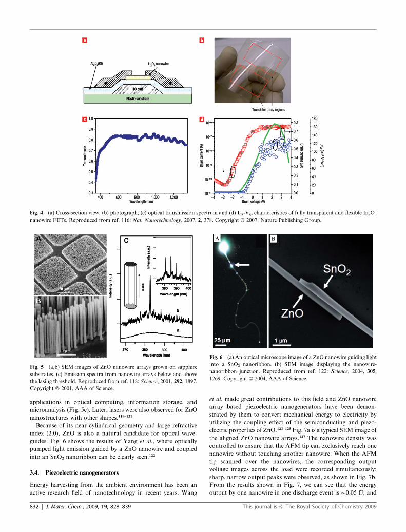
Fig. 4 (a) Cross-section view, (b) photograph, (c) optical transmission spectrum and (d) Ids-Vgs characteristics of fully transparent and flexible In2O3
nanowire FETs. Reproduced from ref. 116: Nat. Nanotechnology, 2007, 2, 378. Copyright ª 2007, Nature Publishing Group.
Fig. 5 (a,b) SEM images of ZnO nanowire arrays grown on sapphire
substrates. (c) Emission spectra from nanowire arrays below and above
the lasing threshold. Reproduced from ref. 118: Science, 2001, 292, 1897.
Copyright ª 2001, AAA of Science.
Fig. 6 (a) An optical microscope image of a ZnO nanowire guiding light
into a SnO2 nanoribbon. (b) SEM image displaying the nanowire-
nanoribbon junction. Reproduced from ref. 122: Science, 2004, 305,
1269. Copyright ª 2004, AAA of Science.
applications in optical computing, information storage, and
microanalysis (Fig. 5c). Later, lasers were also observed for ZnO
nanostructures with other shapes.119–121
Because of its near cylindrical geometry and large refractive
index (2.0), ZnO is also a natural candidate for optical wave-
guides. Fig. 6 shows the results of Yang et al., where optically
pumped light emission guided by a ZnO nanowire and coupled
into an SnO2 nanoribbon can be clearly seen.122
3.4. Piezoelectric nanogenerators
Energy harvesting from the ambient environment has been an
active research field of nanotechnology in recent years. Wang
832 | J. Mater. Chem., 2009, 19, 828–839
et al. made great contributions to this field and ZnO nanowire
array based piezoelectric nanogenerators have been demon-
strated by them to convert mechanical energy to electricity by
utilizing the coupling effect of the semiconducting and piezo-
electric properties of ZnO.123–125 Fig. 7a is a typical SEM image of
the aligned ZnO nanowire arrays.127 The nanowire density was
controlled to ensure that the AFM tip can exclusively reach one
nanowire without touching another nanowire. When the AFM
tip scanned over the nanowires, the corresponding output
voltage images across the load were recorded simultaneously:
sharp, narrow output peaks were observed, as shown in Fig. 7b.
From the results shown in Fig. 7, we can see that the energy
output by one nanowire in one discharge event is �0.05 fJ, and
This journal is ª The Royal Society of Chemistry 2009

Fig. 7 (a) SEM image of aligned ZnO nanowire arrays. (b) Output
voltage image of the nanowire arrays. (c) A series of line profiles of
the voltage output signal. (d) Line profiles from the topography and
output voltage images across a nanowire. (e) Line profile of the voltage
output signal when the AFM tip scans across a vertical nanowire at
12.394 mm/s. (f) The resonance vibration of a nanowire after being
released by the AFM tip. Reproduced from ref. 123: Science, 2006, 312,
242. Copyright ª 2006, AAA of Science.
Fig. 8 (A) Schematic diagram of the ZnO nanowire array DSSC. (B)
Traces of current density against voltage for two different DSSCs. Inset is
a SEM image of aligned ZnO nanowires. Reproduced from ref. 128: Nat.
Mater., 2005, 4, 455. Copyright ª 2005, Nature Publishing Group.
the output voltage on the load is �8 mV. By choosing suitable
nanowire density, the power generated may be high enough to
drive a single nanowire based device. Further exploration of the
piezoelectric nanogenerator concept led to the development of
a wide variety of ZnO nanowire based piezotronic devices,
including piezoelectric field effect transistors, nanoforce sensors,
and gate diodes.126,127
3.5. Solar cells and photocatalysts
In recent years, solar energy conversion devices like solar cells,
which directly converse sunlight into electricity, have attracted
great research interest to solve the continuously increasing
energy problems. Metal oxide nanowires acting as the absorbing
layers can be used to build high performance solar cells. They
also can be used to replace the conventional quantum dot films in
dye-sensitized solar cells (DSSCs). Yang et al. built the first
DSSC using aligned ZnO nanowires as shown in Fig. 8. A direct
conversion efficiency of 1.5% is demonstrated, which is primarily
limited by the surface area of ZnO nanowire arrays.128 Driven by
this work, many DSSCs built on different metal oxide nanowires
This journal is ª The Royal Society of Chemistry 2009
with different conversion efficiencies were demonstrated and the
used metal oxide nanowires include TiO2 nanorods, CuO
nanorods, core/shell ZnO/Al2O3, ZnO/TiO2, ZnO/ZnSe nano-
wires, etc.129–133
Developing semiconductor photocatalysts for water splitting
and degradation of organic pollutants provides another way to
solve the urgent energy and environmental issues.134–137 Metal
oxide nanowires gained much attention in this direction to be
used as high performance photocatalysts due to their extremely
enhanced surface areas.138–145 1-D TiO2 nanostructures, nano-
rods, nanowires and nanotubes, are the mostly investigated oxide
nanostructures that can be used as high performance photo-
catalysts exhibiting better water splitting and organic degradation
properties than bulk materials.138,139 Several other oxide nanowire
photocatalysts include ZnO nanowires, SnO2 nanowires, VO2
nanowire arrays, and many ternary oxide nanowires, such as
SrSnO4 nanowires,142 BiVO4 nanotubes, and AgIn(WO4)2
nanotubes.145 With the development of better synthesis
approaches to 1-D metal oxide nanostructures, photocatalysts
with greatly improved performance are expected to be obtained.
3.6. Field nanoemitters
Field emission, also known as Fowler–Nordheim tunneling, is
a form of quantum tunneling in which electrons pass from an
J. Mater. Chem., 2009, 19, 828–839 | 833

Fig. 9 Field emission properties form vertically aligned ZnO nanowires
grown on a Si substrate. Reproduced from ref. 147: Chem. Phys. Lett.,
2005, 404, 69. Copyright ª 2005, Sciencedirect.
emitting material to the anode through a barrier in the presence
of a high electric field. It is one of the main features of metal
oxide nanowires, and is of great commercial interest in many
areas, such as displays and other electronic devices. Using metal
oxide nanowires as field nanoemitters was first reported by Lee in
2002.146 They studied the field emission properties of vertically-
aligned ZnO nanowires grown via a VS process and found a turn-
on voltage of 6.0 V/mm at a current density of 0.1 mAcm�2
(Fig. 9).147
Inspired by the work using ZnO nanowires as field nano-
emitters, field emission properties of many other kinds of metal
oxide nanowires were also studied, including WO3, IrO2, RuO2,
CuO, TiO2, SnO2, In2O3 nanowires.147–165 Compared with
carbon nanotube based emitteors, metal oxide emitters are more
stable in harsh environments and controllable in electrical
properties.
4. Chemical sensors built on metal oxide nanowires
With large surface-to-volume ratios and a Debye length
comparable to their dimensions, metal oxide nanowires have
showed great potential to be used as chemical sensors.106
Recently, the detection of a wide range of chemicals with
different nanowire sensor configurations has been reported. For
instance, Zhang and coworkers fabricated and tested an In2O3
nanowire mat sensor for which a detection limit of �5 ppb was
achieved.166 Table 2 summarizes a list of typical metal oxide
nanowire based chemical sensors with different device configu-
rations, working temperatures, detection limits and response
times of different targeted chemicals.166–194 As one can see,
chemical sensors built on SnO2, ZnO, and In2O3 nanowires have
been widely reported due to their easy synthesis, good sensitivity
to chemicals, and good stability compared to other metal oxide
nanomaterials. In addition, in spite of their sensitivity, selectivity
of chemical sensors remains one of the challenging issues in this
field.
The sensing mechanism of metal oxide nanowires has been
discussed in recent publications. Briefly, the working principle of
metal oxide nanowire-based chemical sensors relies on changes
834 | J. Mater. Chem., 2009, 19, 828–839
of electrical conductivity due to the interaction of nanowires with
the surrounding environment. The charge transfer process induced
by the redox reactions between nanowire surface and tested
chemicals determines the conductance of nanowire-based chemical
sensors. For example, when a reducing gas (eg. CO) is introduced
to a chemical sensor, the following reaction happens:172
CO + O� / CO2 + e�
Here, CO reacts with adsorbed oxygen ions on the nanowire
surface and thus results in an overall increase of the electrical
conductance of metal oxide nanowires.
On the other hand, if a chemical sensor is exposed to an
oxidation gas (eg. NO2), the following oxidizing reaction may
take place:195
NO2 + e� / NO2�
NO2 serve as charge accepting molecules and withdraw electrons
from the nanowire, resulted in a reduction of electrical conductance.
Based on the above mentioned sensing mechanisms, metal
oxide nanowire-based chemical sensors are usually fabricated in
two configurations, resistors and FET devices with single or
multiple nanowire nanowires. In fact, most reported works in
this field are based on these two configurations due to easy
fabrication, good reliability, low cost, and easy integration with
heat transducers.
Instead of the sensors measuring the change of electrical
conductance, there are several other kinds of sensors, such as
photoluminescence (PL) sensors, and nanostructured ZnO
coated quartz crystal microbalance (QCM) sensors. However,
compared with the electrical chemical sensors, these sensors are
complicated and expensive.
Below we will discuss chemical sensors following different
sensor configurations, i.e. electrical, optical and nanostructure
coated QCM gas sensors and electronic noses, each with one or
two examples.
4.1. Electrical based chemical sensors
A resistor based sensor is one of the easiest methods to carry out
chemical sensing experiments by measuring the change of
conductance of the sensing element in different surrounding
environments. Fig. 10a showed a schematic drawing of a tran-
sistor based chemical sensor. Nanowires are dispersed on a SiO2/
Si substrate followed by patterning source and drain electrodes
above the dispersed nanowires. The Si substrate serves as a back
gate electrode while the chemical sensor works as FET based
sensors. To improve the sensitivity and detect inert gases, several
groups reported to integrate MEMS hotplates with chemical
sensors.178 For instances, Fig. 10b is a SEM image of the active
area of one chemical sensor chip, where the dashed box repre-
sents the SiN membrane and one nanowire is bridged by two
electrodes which can be used as a chemical sensor as shown in
Fig. 10c. The zigzag shaped micromachined hotplates provide
a facile way to control elevated temperatures with low power
consumption. With the aid of elevated temperatures, the detec-
tion limits of this chemical sensor can be enhanced down to 1
ppm for ethanol as shown in Fig. 10d.
This journal is ª The Royal Society of Chemistry 2009

Table
2S
um
ma
ryo
fso
me
typ
ica
lch
emic
al
sen
sors
bu
ilt
on
met
al
ox
ide
na
no
wir
es
Mate
rial
Dev
ice
Dia
met
er(n
m)
An
aly
tes
Det
ect
lim
itR
esp
on
seti
me
(s)
Wo
rkin
gte
mp
era
ture
Sy
nth
esis
met
ho
dR
ef.
In2O
3F
ET
10
NO
2N
H3,
O2
CO
,H
2N
O2
5p
pb
5–
10
RTa
Lase
ra
bla
tio
n1
66
FE
T1
0N
O2,
NH
3N
O2
0.5
pp
mR
TL
ase
ra
bla
tio
n1
67
FE
T1
0N
H3
0.0
02
%N
H3
20
RT
Ch
emic
al
va
po
rd
epo
siti
on
16
8
Sn
O2
Res
isto
ra
nd
ph
oto
lum
ines
cen
cese
nso
r
O2,
CO
,N
O2,
eth
an
ol
CO
10
pp
m;
NH
3
50
pp
m;
NO
21
pp
m3
02
00
� CV
ap
or
ph
ase
dep
osi
tio
n1
69
FE
T6
0O
2,
CO
20
05
50
KE
lect
ro-d
epo
siti
on
17
0F
ET
60
O2,
CO
40
0–5
00
KE
lect
ro-d
epo
siti
on
17
1R
esis
tor
60
O2,
CO
40
50
0K
Ele
ctro
-dep
osi
tio
n1
72
Res
isto
r(A
C)
20
CO
CO
5p
pm
;st
ab
ilit
y4
%1
00
20
–20
0� C
17
3In
-Sn
O2
Res
isto
r7
0–
15
0E
tha
no
l1
0p
pm
24
00
� CT
her
ma
lev
ap
ora
tio
n1
74
Sb
-Sn
O2
Res
isto
r4
0E
tha
no
l1
0p
pm
53
00
� CT
her
ma
lev
ap
ora
tio
n1
75
Ru
-Sn
O2
Res
isto
r1
00
–9
00
NO
2,
liq
uid
pet
role
um
ga
s5
0p
pm
30
–9
02
50
� CT
her
ma
lev
ap
ora
tio
n1
76
Zn
OF
ET
NH
3,
NO
2N
O2
20
0p
pb
,N
H3
0.5
%1
00
17
7F
ET
40
–60
O2
Th
erm
al
evap
ora
tio
n1
78
Res
isto
r3
0E
tha
no
l5
0p
pm
60
RT
-30
0� C
Th
erm
al
evap
ora
tio
n1
79
FE
T6
0O
210
pp
mR
TV
ap
or-
liq
uid
-so
lid
180
Qu
art
zcr
yst
al
mic
ro-b
ala
nce
20
NH
34
0–
10
00
pp
m5
RT
Th
erm
al
evap
ora
tio
n1
81
Res
isto
r3
0–
15
0H
2,
O3
3%
O3
11
2� C
for
H2;
RT
for
O3
MB
E1
82
Pd
,P
t,A
u,
Ni,
Ag
,Ti
do
ped
Zn
OR
esis
tor
30
–15
0H
21
0p
pm
60
0R
TT
her
ma
lev
ap
ora
tio
n1
83
Ga
-Zn
OR
esis
tor
50
–12
5C
O3
20
� CT
her
ma
lev
ap
ora
tio
n1
84
Pd
-Zn
OR
esis
tor
30
–15
0H
21
0p
pm
20
RT
18
5P
t-Z
nO
Res
isto
r3
0–
15
0H
25
00
pp
m6
00
RT
MB
E1
86
Ga
2O
3R
esis
tor
10
–40
NH
3,
NO
2N
H3
20
0p
pm
,N
O2
20
pp
m3
60
24
0G
ao
xid
ized
18
7
Res
isto
r5
0–
90
Eth
an
ol
15
00
pp
m1
00
� CG
ao
xid
ized
18
8W
O3
Res
isto
r1
00
NO
2,
H2S
NO
25
0p
pb
,H
2S
10
pp
mS
ever
al
min
25
0� C
Th
erm
al
evap
ora
tio
n1
89
TeO
2R
esis
tor
30
–20
0N
O2,
NH
3,
H2S
NO
21
0p
pm
,N
H3
10
0p
pm
,H
2S
50
pp
m6
00
RT
Th
erm
al
evap
ora
tio
n1
90
V2O
5R
esis
tor
He
Ele
ctro
-ph
ore
sis
sol-
gel
19
1R
esis
tor
10
1-B
uty
lam
ine,
tolu
ene,
1-p
rop
an
ol
1-B
uty
lam
ine
30
pp
b500
RT
Aq
ueo
us
solu
tio
nm
eth
od
19
2
Zn
Sn
O3
Res
isto
r2
0–
90
Eth
an
ol
1p
pm
13
00
� CT
her
ma
lev
ap
ora
tio
n1
93
Res
isto
r5
0O
2T
her
ma
lev
ap
ora
tio
n1
94
aR
T¼
Ro
om
tem
per
atu
re.
This journal is ª The Royal Society of Chemistry 2009 J. Mater. Chem., 2009, 19, 828–839 | 835

Fig. 10 (a) Schematic diagram of a single nanowire transistor structure.
(b) SEM image of the chemical sensor chip integrated of a single In2O3
nanowire and micromachined hotplates, where the dashed box indicates
the SiN membrane. (c) SEM image of a sensing device with an In2O3
nanowire bridging two electrodes. (d) Sensing response of an In2O3
nanowire sensor operated at 275 �C to four different ethanol concen-
trations (1, 10, 50, and 100 ppm). Reproduced from ref. 196: Appl. Phys.
Lett., 2008, 92, 93111. Copyright ª 2007, AIP.
Fig. 11 Response of a ZnO nanowire FET exposed to 10 ppm NO2 gas.
Reproduced from ref. 180: Appl. Phys. Lett., 2004, 85, 5923. Copyright ª2004, AIP.
In FET based chemical sensors, Fan et al. studied oxygen and
NO2 adsorption on the ZnO nanowire surface by using indi-
vidual ZnO nanowire field-effect transistors.177 The results of
sensing experiments can be observed in Fig. 11. A considerable
variation of conductance was observed when the device was
exposed to oxygen or NO2. In addition, an electrical potential to
the back gate electrode was applied, which could help to adjust
the sensitivity range of the device or initialize the device
completely before exposure to chemicals. This can be attributed
to the fact that the Fermi level within the nanowire band gap was
manipulated by applying an external gate voltage. In addition,
a ZnO chemical sensor was fully refreshed by applying a high
negative gate bias of 60 V as shown in Fig. 11.
Fig. 12 Principal component analysis (PCA) scores and loading plots of
a chemical sensor array composed of four different nanostructure
materials.
4.2. Optical and QCM based chemical sensors
With the novel characterization of contactless devices, recently
several research groups executed chemical sensing experiments
836 | J. Mater. Chem., 2009, 19, 828–839
based on metal oxide nanowire PL chemical sensors, such as
SnO2, and ZnO, etc.197,198 After exposure to chemicals, the
quenching of PL was observed.199 Although the microscopic
mechanisms are still not clear, the quenching is thought to be
related to the change of the oxidation state of the nanowire
surface before and after chemical exposure.197 In addition, the
sensing response time and recovery time are fast (merely a few
seconds), comparable with the response times of most electrical
based chemical sensors. For the QCM based sensor, it is thought
to be a mass-sensitive sensor, which can detect the change of
mass on a sensing layer. The mass of the sensing layer varies due
to the chemical reactions, adsorption, and deposition happening
above the surface of the sensing layer, while the sensor is exposed
to chemicals. QCM based sensors are also contactless devices.200
4.3. Electronic noses
The idea of electronic noses was inspired by the mechanisms of
human olfaction. In general, basic elements of an electronic nose
system include an ‘‘odour’’ sensor array, a data pre-processor,
and a pattern recognition (PARC) engine.201 There are several
methods to approach this goal, one is to make a chemical sensor
array with different nanostructured materials and the other is to
make a sensor chip with different material geometric properties
and temperature gradients (KAMINA technology). Kolmakov
et al. adapted this idea and fabricated a KAMINA sensor chip
composed of SnO2 nanowires with different nanowire densities,
which exhibited good selectivity for several chemicals.202 The
achievement not only successfully solved the ‘‘selectivity’’ issue
but also brought nanotechnology a step closer to practical
application.
Very recently, we developed a new template built with four
different semiconducting nanostructures: In2O3 nanowires, SnO2
nanowires, ZnO nanowires and single-wall C nanotubes (SWNT)
as electronic noses to detect different chemicals (Fig. 12 inset).203
n-Type metal oxide nanowires and p-type C nanotubes provide
one discrimination factor. The integrated micromachined hot
plate enables individual and accurate temperature control of
each sensor, which provides the second discrimination factor.
This journal is ª The Royal Society of Chemistry 2009

When this sensor array was exposed to different chemicals, good
selectivity was obtained to build up an interesting ‘‘smell-print’’
library of the detected chemicals (Fig. 12).
5. Summary
In summary, we provide a comprehensive review of the state-of-
the-art research activities focused on devices and chemical sensing
applications of metal oxide nanowires. The fascinating achieve-
ments, till now, towards the device applications of metal oxide
nanowires should inspire more and more research efforts to address
the remaining challenges in this interesting field. We tried to include
the most important topics in this review article. However, due to the
tremendous research effort and space limitations, this article is
unable to list all the exciting works reported in this field.
Although comprehensive efforts have been made towards the
synthesis of high quality metal oxide nanowires, there is still
plenty of room left unexploited. We believe that future work in
the nanowire synthesis direction should continue to focus on
generating high quality and large quantity metal oxide nanowires
in more controlled, predictable and simple ways. One key issue of
metal oxide nanowires is the growth of p-type metal oxide
nanowires or the formation of intra-nanowire p-n junctions,
which will significantly advance and widen the device application
of metal oxide nanowires.
One interesting area in the metal oxide nanowire based
chemical sensors area is still the development of high quality 1-D
metal oxide nanostructures to be used as chemical sensing
elements. The sensing issues of extremely high sensitivity, selec-
tivity and stability should be resolved. Though some research
groups have successfully detected important chemicals using 1-D
metal oxide nanostructures, the selectivity is still quite low.
Furthermore, other potential and interesting areas which need
further exploration may be the detection of very small amounts
of nerve agents such as sarin and soman, or of explosive chem-
icals for personal health and human security applications.
References
1 P. D. Yang, H. Q. Yan, S. Mao, R. Russo, J. Johnson, R. Saykally,N. Morris, J. Pham, R. R. He and H. J. Cho, Adv. Funct. Mater.,2002, 12, 323.
2 Z. W. Pan, Z. R. Dai and Z. L. Wang, Science, 2001, 291, 1947.3 Y. L. Wang, X. C. Jiang and Y. Xia, J. Am. Chem. Soc., 2003, 125,
16176.4 C. Li, D. Zhang, S. Han, X. Liu, T. Tang and C. Zhou, Adv. Mater.,
2003, 15, 143.5 Y. Kobayashi, H. Hata, M. Salama and T. E. Mallouk, Nano Lett.,
2007, 7, 2142.6 H. W. Ra, K. S. Choi, J. H. Kim, Y. B. Hahn and Y. H. Im, Small,
2008, 4, 1105.7 F. L. Zhang, T. Nyberg and O. Inganas, Nano Lett., 2002, 2, 1373.8 X. Duan and C. M. Lieber, Adv. Mater., 2000, 12, 298.9 C. M. Lieber, MRS Bull., 2003, 28, 486.
10 Y. W. Wang, L. D. Zhang, G. Z. Wang, X. S. Peng, Z. Q. Chu andC. H. Liang, J. Cryst. Growth, 2002, 234, 171.
11 Y. Li, G. W. Meng, L. D. Zhang and F. Phillipp, Appl. Phys. Lett.,2000, 76, 2011.
12 H. Zhang, D. Yang, Y. J. Ji, X. Y. Ma, J. Xu and D. L. Que, J. Phys.Chem. B, 2004, 108, 3955.
13 H. Zhang, D. R. Yang, X. Y. Ma and D. L. Que, J. Phys. Chem. B,2005, 109, 17055.
14 Y. Ding, P. X. Gao and Z. L. Wang, J. Am. Chem. Soc., 2004, 126,2066.
This journal is ª The Royal Society of Chemistry 2009
15 X. Y. Zhang, J. Y. Dai, H. C. Ong, N. Wang, H. L. W. Chan andC. L. Choy, Chem. Phys. Lett., 2004, 393, 17.
16 L. Vayssieres, Adv. Mater., 2003, 15, 464.17 P. X. Gao and Z. L. Wang, J. Phys. Chem. B, 2004, 108, 7534.18 Z. L. Wang, J. Nanosci. Nanotechnl., 2008, 8, 27.19 A. B. Hartanto, X. Ning, Y. Nakata and T. Okada, Appl. Phys. A,
2004, 78, 299.20 Y. J. Xing, Z. H. Xi, Z. Q. Xue, X. D. Zhang, J. H. Song,
R. M. Wang, J. Xu, Y. Song, S. L. Zhang and D. P. Yu, Appl.Phys. Lett., 2003, 83, 1689.
21 X. Kong, X. M. Sun, X. L. Li and Y. D. Li, Mater. Chem. Phys.,2003, 82, 997.
22 Y. Sun, G. M. Fuge, N. A. Fox, D. J. Riley and M. N. R. Ashfold,Adv. Mater., 2005, 17, 2477.
23 Y. K. Liu, C. L. Zheng, W. Z. Wang, C. R. Yin and G. H. Wang,Adv. Mater., 2001, 13, 1883.
24 D. F. Zhang, L. D. Sun, J. L. Yin and C. H. Yan, Adv. Mater., 2003,15, 1022.
25 B. Cheng, J. M. Russell, W. S. Shi, L. Zhang and E. T. Samulski,J. Am. Chem. Soc., 2004, 126, 5972.
26 J. H. He, T. H. Wu, C. L. Hsin, K. M. Li, L. J. Chen, Y. L. Chueh,L. J. Chou and Z. L. Wang, Small, 2006, 2, 116.
27 Z. Liu, D. Zhang, S. Han, C. Li, T. Tang, W. Jin, X. Liu, B. Lei andC. Zhou, Adv. Mater., 2003, 15, 1754.
28 S. Luo, P. K. Chu, W. Liu, M. Zhang and C. L. Lin, Appl. Phys.Lett., 2006, 88, 183112.
29 Y. Chen, X. Cui, K. Zhang, D. Pan, S. Zhang, B. Wang andJ. G. Hou, Chem. Phys. Lett., 2003, 369, 16.
30 S. Sun, G. W. Meng, G. Zhang, T. Gao, B. Geng, L. D. Zhang andJ. Zuo, Chem. Phys. Lett., 2003, 376, 103.
31 J. Duan, S. Yang, H. Liu, J. Gong, H. Huang, X. Zhao, R. Zhangand Y. Du, J. Am. Chem. Soc., 2005, 107, 6180.
32 J. Hu, Y. Bando, Q. Liu and D. Golberg, Adv. Funct. Mater., 2003,13, 493.
33 B. Liu and H. C. Zeng, J. Phys. Chem. B, 2004, 108, 5867.34 N. Du, H. Zhang, B. Chen, X. Ma and D. R. Yang, Chem. Commun.,
2008, 3028.35 N. Wang, X. Cao and L. Guo, J. Phys. Chem. C, 2008, 112, 12616.36 X. S. Peng, G. W. Meng, J. Zhang, X. F. Wang, Y. W. Wang,
C. Z. Wang and L. D. Zhang, J. Mater. Chem., 2002, 12, 1602.37 J. Zhang, X. Qing, F. H. Jiang and Z. H. Dai, Chem. Phys. Lett.,
2003, 371, 311.38 H. Q. Cao, X. Q. Qiu, Y. Liang, Q. Zhu and M. Zhao, Appl. Phys.
Lett., 2003, 83, 761.39 X. Y. Kong and Z. L. Wang, Solid State Commun., 2003, 128, 1.40 Y. Li, Y. Bando and D. Golberg, Adv. Mater., 2003, 15, 581.41 C. Chen, D. Chen, X. Jiao and C. Qang, Chem. Commun., 2006,
4632.42 H. Zhang, Y. Kong, Y. Wang, X. Du, Z. Bai, J. Wang, D. P. Yu,
Y. Ding, Q. Hang and S. Feng, Solid State Commun., 1999, 109, 677.43 Y. C. Choi, W. S. Kim, Y. S. Park, S. M. Lee, D. J. Bae, Y. H. Lee,
G. S. Park, W. B. Choi, N. S. Lee and J. M. Kim, Adv. Mater., 2000,12, 746.
44 J. Hu, Q. Li, X. Meng, C. S. Lee and S. T. Lee, J. Phys. Chem. B,2002, 106, 9536.
45 K. W. Chang and J. J. Wu, Appl. Phys. A, 2003, 76, 629.46 B. Geng, L. D. Zhang, G. W. Meng, T. Xie, X. Peng and Y. Lin,
J. Cryst. Growth, 2003, 259, 291.47 J. Zhagn, F. H. Jiang, Y. Yang and J. Li, J. Phys. Chem. B, 2005,
109, 13143.48 N. Gong, M. Lu, C. Y. Wang, Y. Chen and L. J. Chen, Appl. Phys.
Lett., 2008, 92, 073101.49 K. Zhu, H. He, S. Xie, X. Zhang, W. Zhou, S. Jin and B. Yue, Chem.
Phys. Lett., 2003, 377, 317.50 Y. Baek and K. Yong, J. Phys. Chem. C, 2007, 111, 1213.51 X. Song, Y. Zheng, E. Yang and Y. Wang, Mater. Lett., 2007, 61,
3904.52 Y. Li, Y. Bando, D. Golberg and K. Kurashima, Chem. Phys. Lett.,
2003, 367, 214.53 F. Zhou, X. Zhao, Y. Liu, C. Yuan and L. Li, Eur. J. Inorg. Chem.,
2008, 16, 2506.54 C. K. Chan, H. Peng, R. D. Twesten, K. Jarausch, X. F. Zhang and
Y. Cui, Nano Lett., 2007, 7, 490.55 Y. Yin, G. Zhang and Y. N. Xia, Adv. Funct. Mater., 2002, 12, 293.56 H. W. Kim and S. H. Shim, Chem. Phys. Lett., 2006, 422, 165.
J. Mater. Chem., 2009, 19, 828–839 | 837

57 K. Nagashima, T. Yanagida, H. Tanaka and T. Kawai, J. Appl.Phys., 2007, 101, 124304.
58 J. H. Zhan, Y. Bando, J. Hu and D. Golberg, Inorg. Chem., 2004, 43,2462.
59 H. Imai, Y. Takei, K. Shimizu, M. Matsuda and H. Hirashima,J. Mater. Chem., 1999, 9, 2971.
60 S. Liu, L. Gan, L. Liu, W. Zhang and H. Zeng, Chem. Mater., 2002,14, 1391.
61 Y. Zhang, G. Li, Y. Jin, Y. Zhang, J. Zhang and L. D. Zhang, Chem.Phys. Lett., 2002, 365, 300.
62 J. M. Wu, H. C. Shih and W. T. Wu, Chem. Phys. Lett., 2005, 413,490.
63 H. Cao, X. Qiu, B. Luo, Y. Liang, Y. Zhang, R. Tan, M. Zhao andQ. Zhu, Adv. Funct. Mater., 2004, 14, 243.
64 L. Li and W. Z. Wang, Solid State Commun., 2003, 127, 639.65 C. Dae, S. Kim, B. Ahn, J. Kim, M. Sung and H. Shin, J. Mater.
Chem., 2008, 18, 1362.66 M. Wei, Z. M. Qi, M. Ichihara and H. Zhou, Acta Mater., 2008, 56,
2488.67 B. Varghese, S. C. Haur and C. T. Lim, J. Phys. Chem. C, 2008, 112,
10008.68 S. Hu and X. Wang, J. Am. Chem. Soc., 2008, 130, 8126.69 B. C. Satishkumar, A. Govindaraj, E. M. Vogl, L. Basumallick and
C. N. R. Rao, J. Mater. Res., 1997, 12, 604.70 Y. Li and Y. Bando, Chem. Phys. Lett., 2002, 364, 484.71 J. Zhou, S. Deng, N. S. Xu, J. Chen and J. She, Appl. Phys. Lett.,
2003, 83, 2653.72 B. Qi, X. Ni, D. Li and H. Zheng, Chem. Lett., 2008, 37, 336.73 X. Wang and Y. D. Li, J. Am. Chem. Soc., 2002, 124, 2880.74 M. Imperor-Clerc, D. Bazin, M. D. Appay, P. Beaunier and
A. Davidson, Chem. Mater., 2004, 16, 1813.75 D. Zheng, S. X. Sun, W. Fan, H. Yu, C. Fan, G. Cao, Z. Yin and
X. Song, J. Phys. Chem. B, 2005, 109, 16439.76 Y. Fu, J. Chen and H. Zhang, Chem. Phys. Lett., 2001, 350, 491.77 Y. Xiong, Y. Xie, Z. Li, R. Zhang, J. Yang and C. Wu, New
J. Chem., 2003, 27, 588.78 X. Wen, S. Wang, Y. Ding, Z. L. Wang and S. Yang, J. Phys. Chem.
B, 2005, 109, 215.79 Z. Liu, D. Zhang, S. Han, C. Li, B. Lei, W. Lu, J. Fang and C. Zhou,
J. Am. Chem. Soc., 2005, 127, 6.80 J. Wang, Q. W. Chen, C. Zeng and B. Y. Hou, Adv. Mater., 2004, 16,
137.81 Z. Dong, Y. Y. Fu, Q. Han, Y. Xu and H. Zhang, J. Phys. Chem. C,
2007, 111, 18475.82 H. Zhang, J. Wu, C. Zhai, X. Ma, N. Du, J. Tu and D. R. Yang,
Nanotechnology, 2008, 19, 035711.83 N. Du, H. Zhang, B. Chen, J. Wu, X. Ma, Z. Liu, Y. Zhang,
D. Yang, X. Huang and J. Tu, Adv. Mater., 2007, 19, 4505.84 X. W. Lou, D. Deng, J. Y. Lee, J. Feng and L. A. Archer, Adv.
Mater., 2008, 20, 258.85 R. S. Chen, Y. S. Huang, D. S. Tsai, S. Chattopadhyay, C. T. Wu,
Z. H. Lan and K. H. Chen, Chem. Mater., 2004, 16, 2457.86 Y. L. Chen, C. C. Hsu, Y. H. Song, Y. Chi, A. J. Carty, S. M. Peng
and G. H. Lee, Chem. Vapor. Dep., 2006, 12, 442.87 C. K. Xu, K. Q. Hong, S. Liu, G. H. Wang and X. N. Zhao, J. Cryst.
Growth, 2003, 255, 308.88 Q. Yang, J. Sha, X. Y. Ma and D. R. Yang, Mater. Lett., 2005, 59,
1967.89 C. S. Shi, G. Q. Wang, N. Q. Zhao, X. W. Du and J. J. Li, Chem.
Phys. Lett., 2008, 454, 75.90 W. Z. Wang, G. H. Wang, X. S. Wang, Y. J. Zhan, Y. K. Liu and
C. L. Zheng, Adv. Mater., 2002, 14, 67.91 Y. J. Xiong, Z. Q. Li, R. Zhang, Y. Xie, J. Yang and C. Z. Wu,
J. Phys. Chem. B, 2003, 107, 3697.92 Y. W. Tan, X. Y. Xue, Q. Peng, H. Zhao, T. H. Wang and Y. D. Li,
Nano Lett., 2007, 7, 3723.93 X. C. Jiang, T. Herricks and Y. N. Xia, Nano Lett., 2002, 2,
1333.94 E. Ko, J. Choi, K. Okamoto, Y. Tak and J. Lee, ChemPhysChem.,
2006, 7, 1505.95 G. H. Du and G. Van Tendeloo, Chem. Phys. Lett., 2004, 393, 64.96 X. S. Peng, X. F. Wang, Y. W. Wang, C. Z. Wang, G. W. Meng and
L. D. Zhang, J. Phys. D., 2002, 35, L101.97 D. S. Dhawale, A. M. More, S. S. Latthe, K. Y. Rajpure and
C. D. Lokhande, Appl. Surf. Sci., 2008, 254, 3269.
838 | J. Mater. Chem., 2009, 19, 828–839
98 X. Liu, C. Li, S. Han, J. Han and C. Zhou, Appl. Phys. Lett., 2003,82, 1950.
99 W. Lee, R. Scholz and U. Gosele, Nano Lett., 2008, 8, 2155.100 Y. B. Li, Y. Bando and D. Golberg, Adv. Mater., 2005, 17, 1401.101 D. B. Kuang, Y. P. Fang, H. Q. Liu, C. Frommen and D. Fenske,
J. Mater. Chem., 2003, 13, 660.102 H. Ogihara, M. Sadakane, Y. Nodasaka and W. Ueda, Chem.
Mater., 2006, 18, 4981.103 X. S. Peng, L. D. Zhang, G. W. Meng, X. F. Wang, Y. W. Wang,
C. Z. Wang and G. S. Wu, J. Phys. Chem. B, 2002, 106, 11163.104 R. S. Wagner and W. C. Ellis, Appl. Phys. Lett., 1964, 4, 89.105 T. J. Trentler, K. M. Hickman, S. C. Goel, A. M. Viano,
P. C. Gibbons and W. E. Buhro, Science, 1995, 270, 1791.106 J. G. Lu, P. Chang and Z. Fan, Mater. Sci. Eng. R, 2006, 52, 49.107 Y. Ding and Z. L. Wang, J. Phys. Chem. B, 2004, 108, 12280.108 P. Chang, Z. Fan, D. Wang, W. Tseng, W. Chiou, J. Hong and
J. G. Lu, Chem. Mater., 2004, 16, 5133.109 C. Li, D. Zhang, S. Han, X. Liu, T. Tang and C. Zhou, Adv. Mater.,
2003, 15, 143.110 Z. Liu, D. Zhang, S. Han, C. Li, T. Tang, W. Jin, X. Liu, B. Lei and
C. Zhou, Adv. Mater., 2003, 15, 1754.111 X. Liu, C. Li, S. Han, J. Han and C. Zhou, Appl. Phys. Lett., 2003,
82, 1950.112 Y. Tan, X. Xue, Q. Peng, H. Zhao, T. Wang and Y. Li, Nano Lett.,
2007, 7, 3723.113 B. Xiang, P. Wei, X. Zhang, S. A. Dayeh, D. P. R. Aplin, C. Soci,
D. Yu and D. Wang, Nano Lett., 2007, 7, 323.114 G. D. Yuan, W. J. Zhang, J. Jie, X. Fan, J. A. Zapien, Y. H. Leung,
L. B. Luo, P. F. Wang, C. S. Lee and S. T. Lee, Nano Lett., 2008, 8,2591.
115 K. Nomura, H. Ohta, K. Ueda, T. Kamiya, M. Hirano andH. Hosono, Science, 2003, 300, 1269.
116 S. Ju, A. Facchetti, Y. Xuan, J. Liu, F. Ishikawa, P. Ye, C. Zhou,T. J. Marks and D. B. Janes, Nat. Nanotech., 2007, 2, 378.
117 S. Ju, J. Li, J. Liu, P. Chen, Y. Ha, F. Ishikawa, H. Chang, C. Zhou,A. Facchetti, D. B. Janes and T. J. Marks, Nano Lett., 2008, 8, 997.
118 M. Huang, S. Mao, H. Feick, H. Yan, Y. Wu, H. Kind, E. Weber,R. Russo and P. Yang, Science, 2001, 292, 1897.
119 J. Johnson, H. Yan, R. Schaller, L. Haber, R. Saykally and P. Yang,J. Phys. Chem. B, 2001, 105, 11387.
120 H. Kind, H. Yan, M. Law, B. Messer and P. Yang, Adv. Mater.,2002, 14, 158.
121 H. Yan, R. He, J. Johnson, M. Law, R. J. Saykally and P. Yang,J. Am. Chem. Soc., 2003, 125, 4728.
122 M. Law, D. Sirbuly, J. Johnson, J. Goldberger, R. Saykally andP. Yang, Science, 2004, 305, 1269.
123 Z. L. Wang and J. Song, Science, 2006, 312, 242.124 X. Wang, J. Song, J. Liu and Z. L. Wang, Science, 2007, 316, 102.125 Y. Qin, X. Wang and Z. L. Wang, Nature, 2008, 451, 809.126 X. Wang, J. Zhou, J. Song, J. Liu, N. Xu and Z. L. Wang, Nano
Lett., 2006, 6, 2768.127 J. H. He, C. L. Hsin, J. Liu, L. J. Chen and Z. L. Wang, Adv. Mater.,
2007, 19, 781.128 M. Law, L. E. Greene, J. C. Johnson, R. Saykally and P. Yang,
Nature Mater., 2005, 4, 455.129 J. T. Liu, F. M. Wang, S. Isoda and M. Adachi, Chem. Lett., 2005,
34, 1506.130 L. Greene, M. Law, B. Yuhas and P. Yang, J. Phys. Chem. C, 2007,
111, 18451.131 M. Law, L. Greene, A. Radenovic, T. Kuykendall, J. Liphardt and
P. Yang, J. Phys. Chem. B, 2006, 110, 22652.132 S. Anandan, X. Wen and S. Yang, Mater. Chem. Phys., 2005, 93, 35.133 K. Wang, J. Chen, W. Zhou, Y. Zhang, Y. Yan, J. Pern and
A. Mascarenhas, Adv. Mater., 2008, 20, 3248.134 A. Fujishimam and K. Honda, Nature, 1972, 238, 37.135 M. R. Hoffmann, S. T. Martin, W. Choi and D. W. Bahnemann,
Chem. Rev., 1995, 95, 69.136 H. Choi, A. C. Sofranko and D. D. Dionysiou, Adv. Funct. Mater.,
2006, 16, 1067.137 S. J. Hwang, C. Petucci and D. Raftery, J. Am. Chem. Soc., 1997,
119, 7877.138 C. Wu, L. Lei, X. Zhu, J. Yang and Y. Xie, Small, 2007, 9, 1518.139 Y. Mao and S. S. Wong, J. Am. Chem. Soc., 2006, 128, 8217.140 G. Wang, W. Lu, J. Li, J. Choi, Y. Jeong, S. Y. Choi, J. B. Park,
M. K. Ryu and K. Lee, Small, 2006, 2, 1436.
This journal is ª The Royal Society of Chemistry 2009

141 Y. Wang, Z. Zhang, Y. Zhu, Z. Li, R. Vajtai, L. Ci andP. M. Ajayan, ACS Nano, 2008, 2, 1492.
142 D. Chen and J. Ye, Chem. Mater., 2007, 19, 4585.143 Y. Yu and D. Xu, Appl. Cata. B, 2007, 73, 166.144 T. J. Kuo, C. N. Lin, C. L. Kuo and M. H. Huang, Chem. Mater.,
2007, 19, 5143.145 L. Zhou, W. Wang, L. Zhang, H. Xu and W. Zhu, J. Phys. Chem. C,
2007, 111, 13659.146 C. J. Lee, T. J. Lee, S. C. Lyu, Y. Zhang, H. Ruh and H. J. Lee, Appl.
Phys. Lett., 2002, 81, 3648.147 H. Ham, G. Z. Shen, J. H. Cho, T. J. Lee, S. H. Seo and C. J. Lee,
Chem. Phys. Lett., 2005, 404, 69.148 G. Z. Shen, Y. Bando, B. D. Liu, D. Golberg and C. J. Lee, Adv.
Funct. Mater., 2006, 16, 410.149 Y. K. Tseng, C. J. Huang, H. M. Cheng, I. N. Lin, K. S. Liu and
I. C. Chen, Adv. Funct. Mater., 2003, 13, 811.150 C. X. Xu and X. W. Sun, Appl. Phys. Lett., 2003, 83, 3806.151 Y. B. Li, Y. Bando and D. Golberg, Appl. Phys. Lett., 2004, 84,
3603.152 D. Banerjee, S. H. Jo and Z. F. Ren, Adv. Mater., 2004, 16, 2028.153 Y. H. Baek and K. J. Yong, J. Phys. Chem. C, 2007, 111, 1213.154 Y. B. Li, Y. Bando and D. Golberg, Adv. Mater., 2003, 15, 1294;
J. Zhou, L. Gong, S. Z. Deng, J. Chen, J. C. She, N. S. Xu,R. S. Yang and Z. L. Wang, Appl. Phys. Lett., 2005, 87, 223108.
155 M. T. Chang, L. J. Chou, Y. L. Chueh, Y. C. Lee, C. H. Hsieh,C. D. Chen, Y. W. Lan and L. J. Chen, Small, 2007, 3, 658.
156 J. G. Liu, Z. J. Zhang, Y. Zhao, X. Su, S. Liu and E. G. Wang,Small, 2005, 1, 310.
157 C. S. Hsieh, D. S. Tsai, R. S. Chen and Y. S. Huang, Appl. Phys.Lett., 2004, 85, 3860.
158 C. L. Cheng, Y. F. Chen, R. S. Chen and Y. S. Huang, Appl. Phys.Lett., 2005, 86, 103104.
159 Y. W. Zhu, A. M. Moo, T. Yu, X. J. Xu, X. Y. Gao, Y. J. Liu,C. T. Lim, Z. X. Shen, C. K. Ong, A. T. S. Wee, J. T. L. Thongand C. H. Sow, Chem. Phys. Lett., 2006, 419, 458.
160 J. Chen, S. Z. Deng, N. S. Xu, W. X. Zhang, X. G. Wen andS. H. Yang, Appl. Phys. Lett., 2003, 83, 746.
161 J. M. Wu, H. C. Shih and W. T. Wu, Chem. Phys. Lett., 2005, 413,490.
162 J. H. He, T. H. Wu, C. L. Hsin, K. M. Li, L. J. Chen, Y. L. Chueh,L. J. Chou and Z. L. Wang, Small, 2006, 2, 116.
163 Y. J. Chen, Q. H. Li, Y. X. Liang, T. H. Wang, Q. Zhao andD. P. Yu, Appl. Phys. Lett., 2004, 85, 5682.
164 S. Q. Li, Y. X. Liang and T. H. Wang, Appl. Phys. Lett., 2006, 88,053107.
165 S. Kar, S. Chakrabarti and S. Chaudhuri, Nanotechnology, 2006, 17,3058.
166 D. Zhang, Z. Liu, C. Li, T. Tang, X. Liu, S. Han, B. Lei andC. Zhou, Nano Lett., 2004, 4, 1919.
167 C. Li, D. Zhang, X. Liu, S. Han, T. Tang, J. Han and C. Zhou, Appl.Phys. Lett., 2003, 82, 1613.
168 C. Li, D. Zhang, B. Lei, S. Han, X. Liu and C. Zhou, J. Phys. Chem.B, 2003, 107, 12451.
169 C. Baratto, E. Comini, G. Faglia, G. Sberveglieri, M. Zha andA. Zappettini, Sens. Actuators B, 2005, 109, 2.
170 X. Y. Xue, Y. J. Chen, Y. G. Liu, S. L. Shi, Y. G. Wang andT. H. Wang, Appl. Phys. Lett., 2006, 88, 201907.
171 Y. Zhang, A. Kolmakov, S. Chretien, H. Metiu and M. Moskovits,Nano Lett., 2004, 3, 403.
172 A. Kolmakov, Y. Zhang, G. Cheng and M. Moskovits, Adv. Mater.,2003, 15, 997.
This journal is ª The Royal Society of Chemistry 2009
173 F. Hernandez-Ramirez, A. Tarancon, O. Casals, J. Arbiol,A. Romano-Rodriguez and J. R. Morante, Sens. Actuators B,2007, 121, 3.
174 X. Y. Xue, Y. J. Chen, Y. G. Liu, S. L. Shi, Y. G. Wang andT. H. Wang, Appl. Phys. Lett., 2006, 88, 201907.
175 Q. Wan and T. H. Wang, Chem. Commun., 2005, 3841.176 N. S. Ramgir, I. S. Mulla and K. P. Vijayamohanan, Sens. Actuators
B, 2005, 107, 708.177 Z. Fan and J. G. Lu, Appl. Phys. Lett., 2005, 86, 123510.178 Q. Wan, Q. H. Li, Y. J. Chen, T. H. Wang, X. L. He and J. P. Li,
Appl. Phys. Lett., 2004, 85, 6389.179 T.-J. Hsueh, C.-L. Hsu, S.-J. Chang and I. C. Chen, Sens. Actuators
B, 2007, 126, 473.180 Z. Fan, D. Wang, P. Chang, W.-Y. Tseng and J. G. Lu, Appl. Phys.
Lett., 2004, 85, 5923.181 X. Wang, J. Zhang and Z. Zhu, Appl. Surf. Sci., 2006, 252, 2404.182 B. S. Kang, Y. W. Heo, L. C. Tien, D. P. Norton, R. Ren, B. P. Gila
and S. J. Pearton, Appl. Phys. A, 2005, 80, 1029.183 H. T. Wang, B. S. Kang, F. Ren, P. W. Sadic, D. P. Norton,
S. J. Pearton and J. Lin, Appl. Phys. A, 2005, 81, 1117.184 T.-J. Hsueh, Y.-W. Chen, S.-J. Chang, S.-F. Wang, C.-L. Hus, Y.-
R. Lin, T.-S. Lin and I. C. Chen, Sens. Actuators B, 2007, 125, 498.185 H. T. Wang, B. S. Kang, F. Ren, L. C. Tien, P. W. Sadik,
D. P. Norton and S. J. Pearton, Appl. Phys. Lett., 2005, 86, 243503.186 L. C. Tien, H. T. Wang, B. S. Kang, F. Ren, P. W. Sadik,
D. P. Norton, S. J. Pearton and J. Lin, Electrochem and SolidState Lett., 2005, 9, G230.
187 Y. Huang, S. Yue, Z. Wang, Q. Wang, C. Shi, Z. Xu, X. D. Bai,C. Tang and C. Gu, J. Phys. Chem. B, 2006, 110, 796.
188 M. F. Yu and M. Z. Atashbar, IEEE Sensors, 2005, 5, 20.189 A. Ponzoni, E. Comini, G. Sbergeglieli, J. Zhou, S. Z. Deng,
N. S. Xu, Y. Ding and Z. L. Wang, Appl. Phys. Lett., 2006, 88,203101.
190 Z. Liu, T. Yamazki, Y. Shen and T. Kikuta, Appl. Phys. Lett., 2007,90, 173119.
191 H. Y. Yu, B. H. Kang, U. H. Pi, C. W. Park and S.-Y. Choi, VAppl.Phys. Lett., 2005, 86, 253102.
192 I. Raible, M. Burghard, U. Schlecht, A. Yasuda and T. Vossever,Sens. Actuators B, 2005, 106, 730.
193 X. Y. Xue, Y. J. Chen, Y. G. Wang and T. H. Wang, Appl. Phys.Lett., 2005, 86, 233101.
194 X. Y. Xue, P. Feng, Y. G. Wang and T. H. Wang, Appl. Phys. Lett.,2007, 91, 022111.
195 C. Baratto, E. Comini, G. Faglia, G. Sberveglieri, M. Zha andA. Zappettini, Sens. Actuators B, 2005, 109, 2.
196 K. Ryu, D. Zhang and C. Zhou, Appl. Phys. Lett., 2008, 92, 93111.197 A. Setaro, A. Bismuto, S. Lettieri, P. Maddalena, E. Comini,
S. Bianchi, C. Baratto and Sberveglieri, Sens. Actuators B, 2008,130, 391.
198 E. Comini, C. Baratto, G. Faglia, M. Ferroni and G. Sberveglieri,J. Phys. D. Appl. Phys., 2007, 40, 7255.
199 G. Faglia, C. Baratto, G. Sberveglieri, M. Zha and A. Zappettini,Appl. Phys. Lett., 2005, 86, 011923.
200 X. Zhou, J. Zhang, T. Jiang, X. Wang and Z. Zhu, Sens. ActuatorsA, 2007, 135, 209.
201 M. A. Craven, J. G. Gardner and P. N. Bartlett, Trends in AnalyticalChemistry, 1996, 15, 486.
202 V. V. Sysoev, J. Goschnick, T. Schneider, E. Strelcov andA. Kolmakov, Nano Lett., 2007, 7, 3182.
203 P. C. Chen, F. N. Ishikawa, H. K. Chang, K. Ryu, and C. Zhou,unpublished results.
J. Mater. Chem., 2009, 19, 828–839 | 839