design of microheater for mems based gas ......table 1.1 temperature limit of some selected metal...
TRANSCRIPT

DESIGN OF MICROHEATER FOR MEMS BASED GAS
SENSOR
Dissertation submitted
in partial fulfillment of the requirement for the award of degree
MASTER OF ENGINEERING
in
ELECTRONICS AND COMMUNICATION
Submitted by
Palakkumar Bhatt
Roll No.: 801061019
Under supervision of
Dr. Anil Arora
Assistant Processor, ECE Department
ELECTRONICS AND COMMUNICATION
ENGINEERING DEPARTMENT
THAPAR UNIVERSITY, PATIALA-147004 (PUNJAB), INDIA
(Established under the section 3 of UGC Act, 1956)
June-2014

iii
ACKNOWLEDGEMENT
I would like to give special thanks to my guide Dr. Anil Arora (Assistant Professor) ECED,
Thapar University, Patiala, for his valuable advice and splendid supervision. It has been a
great honour to work under his guidance. It was his valuable discussions and endless
endeavors through which I gained a lot. His constant encouragement and confidence-
imbibing attitude has always been a moral support for me.
I am thankful to Dr. Sanjay Sharma, Professor and Head, Electronics and communication
Engineering Department, for providing us with adequate infrastructure in carrying the work.
I am also thankful to Dr. Kulbir Singh P.G. Coordinator, Electronics and communication
Engineering Department for the motivation and inspiration that triggered me for the report
work.
I am greatly indebted to all of my friends who constantly encouraged me and also I would
like to thank all the faculty members of ECED for the full support of my work. I am also
thankful to the authors whose work have been consulted and quoted in this thesis. I thank all
those who have contributed directly or indirectly to this work.
Lastly, I would like to thank my family for their years of unyielding love and for constant
support and encouragement. They have always wanted the best for me and I admire their
determination and sacrifice.
Palakkumar Bhatt

iv
ABSTRACT
We introduce design of micro heater for MEMS based gas sensor for detection various gases
in the surrounding environment. MEMS based gas sensors are widely used as they have
several advantages like, higher performance, smaller size, ruggedness, low power
consumption and low cost. Also metal oxide based sensing surfaces are used with their
enormous benefits such as very low cost, high sensitivity, fast response/recovery time, simple
electronic interface, ease of use, low maintenance and ability to detect large number of gases.
Metal oxide sensor which uses electron depleted surface, either oxidation or reduction
process occur on depleted sensing surface (oxide surface) while detection of hazardous gases.
In these process electrons are added or extracted depending on metal oxide sensor whether is
n-type or p-type. These processes change electrical properties of sensing surface. For
oxidation and reduction processes, we need to have high temperature and this can be
achieved by placing micro heater below the metal oxide sensing surface.
Micro-Heaters have been the subject of great interest owing to their extensive applications in
gas sensors, humidity sensors and other micro-systems. A micro-heater should have high
temperature to desired level, low power consumption and better temperature uniformity. My
work is to geometric optimization of the micro-heater structure to achieve temperature
uniformity. Also to compare parameters like, current density distribution, resistance, power
consumption and transient temperature response for Poly-Si and Platinum based micro-
heater. Different geometries are simulated using COMSOL Multiphysics 4.3 to find out best
micro-heater geometry i.e. modified spiral geometry which gives better temperature
uniformity. Also effect of voltage variation on temperature and dimensions variation on
temperature are simulated and analyzed for Poly-Si and Platinum based micro-heater. After
simulations and analysis, conclusion is made by parameters comparison to reach best
solution among Poly-Si and Platinum based micro-heaters.

v
TABLE OF CONTENTS
DECLARATION ii
ACKNOWLEDGEMENT iii
ABSTRACT iv
TABLE OF CONTENTS v
LIST OF FIGURES viii
LIST OF TABLES xi
CHAPTER 1
1.1 Introduction 1
1.1.1 MEMS: An Introduction 1
1.1.2 History of MEMS 3
1.1.3 MEMS Materials 3
1.1.4 Advantages of MEMS 5
1.1.5 Applications of MEMS 5
1.2 Concept of Electronic-Nose (E-nose) 6
1.2.1 E-nose sensor response to odorants 7
1.2.2 Applications of E-nose sensor 8
1.3 Metal Oxide Gas Sensor 9

vi
1.4 Need of micro-heater 10
1.5 Structure of metal oxide based gas sensor 10
1.6 Literature Review 13
1.7 Objectives 17
1.8 Thesis Organization 17
CHAPTER-2
2.1 COMSOL Multiphysics: An Introduction 19
2.2 Joule Heating and Thermal Expansion Interface 22
2.3 Electro – Thermal Mathematical Modeling in Joule Heating 24
2.4 Model Inputs 25
2.5 Conclusion 27
CHAPTER-3
3.1 Sensor design parameters 28
3.2 Micro-heater 30
3.3 Design parameters of micro-heater 30
CHAPTER-4
4.1 Selection of micro-heater material 33
4.2 Micro-heater geometries and their simulation results 33
4.3 Conclusion 37
CHAPTER-5
5.1 Parameters consideration under electro – thermal analysis 39
5.2 Electro-Thermal analysis 39
5.3 Effect of width variation in micro-heater geometry 44
5.4 Simulation of Poly-Si based modified spiral geometry 46

vii
5.5 Simulation of Platinum based modified spiral geometry 53
5.6 Conclusion 61
CHAPTER-6
6.1 Fabrication steps of MEMS based gas sensor 62
6.1.1 Wafer Cleaning 62
(A) Piranha Cleaning 62
(B) RCA-1 Cleaning 63
(C) RCA-2 Cleaning 64
6.1.2 Oxidation 65
6.1.3 Lithography 65
6.1.4 Platinum deposition 66
6.1.5 Silicon nitride deposition (sputtering) and annealing 67
6.1.6 Back side membrane patterning and Oxide Etching 67
6.1.7 Silicon etching using KOH + IPA and TMAH solution 68
6.1.8 Silicon Nitride Removal 69
6.1.9 IDT deposition 69
6.1.10 Deposition of Sensing Layer 69
CHAPTER-7
7.1 Conclusion 70
7.2 Future Scope 71
REFERENCES 73
APPENDIX-I 77
LIST OF PUBLICATION 78

viii
LIST OF FIGURES
Figure No. Description Page No
Fig. 1.1 Basic block diagram of MEMS 2
Fig. 1.2(a) Vectorial representation of sensor in energy domain space 2
Fig. 1.2(b) Vectorial representation of actuator in energy domain space 2
Fig. 1.3 Basic structure of metal oxide based gas sensor 11
Fig. 2.1 COMSOL Multiphysics window 19
Fig. 2.2 Setup study type in COMSOL Multiphysics 20
Fig. 2.3 Joule Heating and Thermal Expansion module window 23
in COMSOL Multiphysics
Fig. 2.4 Material Selection in COMSOL Multiphysics 4.3 26
Fig. 3.1 A structure of micro-heater 31
Fig. 4.1 Single Meander geometry 34
Fig. 4.2 Simulated Single Meander geometry 34
Fig. 4.3 Double Meander geometry 35
Fig. 4.4 Simulated Double Meander geometry 35
Fig. 4.5 Fan type geometry 35
Fig. 4.6 Simulated Fan type geometry 35
Fig. 4.7 S-type geometry 36
Fig. 4.8 Simulated S-type geometry 36
Fig. 4.9 Spiral geometry 36
Fig. 4.10 Simulated Spiral geometry 36
Fig. 4.11 Modified Spiral geometry 37
Fig. 4.12 Simulated Modified Spiral geometry 37
Fig. 5.2.1 3D view of Poly-Si based modified spiral geometry 41
Fig. 5.2.2 2D view of modified spiral geometry with dimensions 41
Fig. 5.2.3 Maximum temperature with variations in applied voltages 42
for Poly-Si based micro-heater
Fig. 5.2.4 Change in thickness Vs maximum temperature characteristic 43
Fig. 5.3.1 3D view of double meander geometry 44
Fig. 5.3.2 2D view of double meander geometry with dimensions 44

ix
Fig. 5.3.3 3D view of changed width double meander geometry 45
Fig. 5.3.4 2D view of change width double meander geometry with 45
dimensions
Fig. 5.3.5 Simulated result for double meander geometry 46
Fig. 5.3.6 Simulated result for changed width double meander geometry 46
Fig. 5.4.1 Simulated Poly-Si based modified spiral geometry 46
Fig. 5.4.2 Current density of Poly-Si based modified spiral geometry 47
Fig. 5.4.3 Transient response of resistance of Poly-Si based modified spiral 47
geometry
Fig. 5.4.4 Transient response of power consumption of Poly-Si based 48
modified spiral geometry
Fig. 5.4.5 Transient temperature response of Poly-Si based modified 48
spiral geometry
Fig. 5.4.6 3D view of Poly-Si based changed width modified spiral 49
geometry
Fig. 5.4.7 2D view with dimensions of Poly-Si based changed width 49
modified spiral geometry
Fig. 5.4.8 Simulated Poly-Si based modified spiral changed width 50
geometry
Fig. 5.4.9 Current density of Poly-Si based changed width modified 50
spiral geometry
Fig. 5.4.10 Transient response of resistance of Poly-Si based changed 51
width modified spiral geometry
Fig. 5.4.11 Transient response of power consumption of Poly-Si based 51
changed width modified spiral geometry
Fig. 5.4.12 Transient temperature response of Poly-Si based changed 52
width modified spiral geometry
Fig. 5.5.1 Simulated Platinum based modified Spiral geometry 53
Fig. 5.5.2 Maximum temperature with variations in applied voltages 54
for Platinum based micro-heater
Fig. 5.5.3 Change in thickness Vs maximum temperature characteristic 54

x
Fig. 5.5.4 Current density of Platinum based modified spiral geometry 55
Fig. 5.5.5 Transient response of Platinum based micro-heater resistance 56
Fig. 5.5.6 Transient response of power consumption of Platinum 56
based modified spiral geometry
Fig. 5.5.7 Transient temperature response of Platinum based modified 57
spiral geometry
Fig. 5.5.8 Simulated Platinum based changed width micro-heater geometry 57
Fig. 5.5.9 Current density of Platinum based changed width modified 58
spiral geometry
Fig. 5.5.10 Transient response of Platinum based changed width 58
micro-heater resistance
Fig. 5.5.11 Transient response of power consumption of Platinum based 59
changed width modified spiral geometry
Fig. 5.5.12 Transient temperature response of Platinum based changed 59
width modified spiral geometry
Fig. 6.1 Silicon wafer <100> as substrate 62
Fig. 6.1.2 Structure after wet oxidation 65
Fig. 6.1.3 Top view of mask lay out design of micro-heater with dimension 66
Fig. 6.1.4 Structure after Platinum deposition 66
Fig. 6.1.5 Structure after Silicon Nitride deposition 67
Fig. 6.1.6 Structure after membrane patterning and Oxide Etching 68
Fig. 6.1.7 Structure after Silicon etching using KOH + IPA and TMAH 69
solution
Fig. 6.1.8 Structure after removal of Silicon Nitride 69
Fig. 6.1.9 IDT structure for detection of resistance change of sensing 69
surface

xi
LIST OF TABLES
Table No. Description Page No.
Table 1.1 Temperature limit of some selected metal oxide sensing 12
surfaces used in gas sensors
Table 1.2 Typically used metal oxide sensing surface and their aimed gases 12
Table 5.2.1 Effect of thickness variation of micro-heater on other parameters 43
for Poly-Si
Table 5.4.1 Comparison of parameters of two geometries for Poly-Si 52
Table 5.5.1 Effect of thickness variation of micro-heater on other parameters for 55
Platinum
Table 5.5.2 Comparison of parameters of two geometries for Platinum 60
Table 5.5.3 Parameters comparison of modified spiral geometry for Poly-Si 60
and Platinum
Table 5.5.4 Parameters comparison of modified spiral geometry with 61
changed width for Poly-Si and Platinum

1
CHAPTER-1
1.1 Introduction
In 21st century, there is growing interest to minimize the size and the power
consumption of any electronic device. There are many technologies introduced but the
most optimistic technology is identified as MEMS.
1.1.1 MEMS: An Introduction
MEMS is known as Micro Electro Mechanical System. It is also known as micro
system technology (MST) in Europe and micro system in Japan. It is process technology
used to generate micro level integrated system or devices that have combination of
mechanical and electrical components. Generalized definition of MEMS can be given as
“It is device where micro sensor and mechanical parts (Actuators) along with signal
processing circuitry are combined on very tiny piece of silicon.” MEMS components
generally have micron level dimensioned part, with a moving element which may be solid
mechanics type or may fluid one, integrated with some electronic circuit. MEMS is
produced using lithography and etching techniques. Besides silicon as substrate other
materials like, quartz, glass and polymer are also used as substrate in MEMS devices [1].
Many machines can be built at the same time on the surface of the wafer, without any
assembly that is real power of MEMS technology.
MEMS is combination of three basic blocks named as sensor, processor and
actuator as shown in Fig. 1.1. Sensor or micro sensor is first block which senses the
measurand or input signal. Most of time input is probably non - electrical signal which
converts into electrical signal. Non electrical signals may be different possible signals
like, thermal, radiation, mechanical, magnetic, optical or bio (chemical). All signals must
be converted into electrical signal by sensor using available possible methods of
conversion. The basic work with of sensor is shown with vectorial representation in Fig.
1.2(a). Processor is next to sensor block which gets electrical signal from sensor. It does
some mathematical or logical operations (decision making operations) on signal.
Processor has electrical signal as input and output. The final building block is actuator
which has electrical signal from processor as input and generally non - electrical signal as
output. It does exactly opposite conversion of signal that is discussed in sensor. It
converts electrical signal into non – electrical signals like, thermal, radiation, mechanical,

2
magnetic, optical or bio (chemical). Actuator’s work can be explained with vectorial
representation as shown in Fig. 1.2(b). Actuator actually responds to environment (e.g.
pumping, filtering, positioning, regulating and moving) based on intended designed
instruction [2].
Input (Measurand) Output
Fig. 1.1 Basic block diagram of MEMS
Sensor Actuator
(a) (b)
Fig. 1.2 Vectorial representation of (a) sensor (b) actuator in energy domain space
where E-Electrical, T-Thermal, R-Radiation, Me-Mechanical, M-Magnetic, O-Optical,
C - Chemical (Bio)
For fabrication of MEMS, three processing steps are used: (1) Deposition (2)
Lithography and (3) Etching. In deposition, thin films of material are deposited on
substrate. Two major methods are used for deposition. One is chemical reaction methods
which are like, chemical vapor deposition (CVD), Electro deposition, epitaxy and thermal
oxidation. Other one is physical reaction methods which are like, physical vapor
deposition (PVD) and casting. In lithography, a patterned mask is applied on top of the
film by photolithographic imaging. It can be classified in two groups: (1) Pattern transfer
and (2) Lithographic module. In etching process, it is necessarily requirement to etch the
E
T
R
Me M
O
C
E
T
R
M
O
C
Me
Sensor
Processor or
Decision
making
operator
Actuator

3
films selectively to the mask. Basically, it is subdivided in two methods: dry etching and
wet etching.
1.1.2 History of MEMS
MEMS was first developed in the 1970s and then it was commercialized in the
1990s. Using MEMS, it becomes possible to make any system to be smaller, more
efficient, less expensive and faster. In an ideal MEMS configuration, ICs (Integrated
Circuits) provide the “thinking” part of that system, while MEMS supplement this
intelligence with control functions and perception [3]. Pressure sensors having bulk
etched silicon structure were the first wave of MEMS commercialization started in the
late 1970s and early 1980s. In that first pressure sensor silicon membrane deformed under
pressure and piezoresistive track laid on its surface, was affected and the change is used
to transform the pressure into an electronic signal [4].
A second wave of commercialization arrived in the 1990s, which was mainly
focused on information technology and personal computers (PCs). In this era, video
projection is one of the products that was introduced by Texas Instrument which is
depended on electrostatic actuated tilting micro mirror arrays. There is another product
named thermally operated inkjet print head that remain a high demand application till
date.
A micro-optics as an accompaniment to optical fiber communication - by way of
all optical related devices and optical switches is the third generation of MEMS
commercialization [5]. And the fourth wave of the commercialization could be other
applications that may include biological and neural probes, also called lab-on-chip drug
development and biochemical system and macroscale drug delivery system. E-nose is
also the latest application that comes under fourth generation of MEMS
commercialization.
1.1.3 MEMS Materials
MEMS technology may be implemented using different manufacturing techniques
and different materials that are totally depend on the device which is being created and
the market in which it has to operate [6]. There are different available choices of materials
available, as mentioned below:

4
Silicon
It is the material which is widely used in consumer electronics of the modern
industry to create most of the integrated circuits. The cost advantage which gets bigger
with increase in output of product, ready availability (abundant), cost effective high
quality materials, also capability to incorporate electronic functionality make silicon as
attractive choice for a various MEMS applications. It has very suitable material properties
among other choices like; it can survive in harsh conditions, has uniform mechanical
properties throughout the wafer lots, and also has suitable mechanical, thermal, electrical
and optical integration. In a form of single crystal, silicon is considered as almost perfect
example of Hookean material, that when it is flexed, there is almost no energy dissipation
because it has virtually no hysteresis. Also silicon has very high reliability as this material
suffers very little fatigue and also has service lifetime in the range of billions to trillions.
And the biggest advantage is fabrication and treatment processes for silicon substrate are
documented and well established. Also silicon compounds are also used in MEMS. Some
of the examples are Silicon dioxide (SiO2), Poly-Silicon (Poly-Si), Silicon Carbide (SiC)
and Silicon Nitride (Si3N4)
Quartz
It is basically a compound of Silicon dioxide (SiO2) and its orientation is not
based on Miller indices. It is also counted as an ideal choice of material for MEMS sensor
as it has near absolute thermal dimensional stability. It is advisable material in case of
micro fluidics applications in biomedical analysis. It has certain advantages over silicon
that it is more dimensionally stable, more flexible in geometry and transparent to
ultraviolet light which is better for motive of species detection.
Gallium Arsenide (GaAs)
It is compound semiconductor and is a major candidate for photonics devices as it
has high mobility of electrons. It is higher level thermal insulator having outstanding
dimensional stability at high temperature. Though it has certain disadvantages compared
with silicon like, more difficult to process and more expensive.
Polymers
They are nowadays become popular choice for MEMS and micro system though
having biggest drawback of poor conductivity. They have certain proficient advantages
like, low cost of raw material, light weight, high electrical resistance, high flexible

5
structure, high corrosion resistance, and also high dimensional stability. Basically they are
divided in two groups: thermoplastics which can be easily formed into desired shape and
thermosets which have better temperature resistance up to 350o C and good mechanical
strength.
Metals
Metals are generally used to make MEMS elements. Although metals do not have
a few advantages which are displayed by silicon materials in terms of mechanical
properties, it can exhibit very high degrees of reliability. Metals are deposited by different
processes; some of them are electroplating, sputtering and evaporation. Widely used
metals in MEMS are: gold, aluminum, platinum, silver, tungsten, copper, nickel, titanium
and chromium.
1.1.4 Advantages of MEMS
Lower Power Consumption
Miniaturization Smaller
Ruggedness
IC Compatible Higher Performance
Batch Fabrication Low Cost
1.1.5 Applications of MEMS
There are so many possible applications for MEMS. Currently, MEMS are most
often found as sensors as gas sensors, pressure sensors, optical sensors, position and
speed micro sensors but the appliances are making large inroads into defense, medical,
aviation, and optical communication [2,3].
Biotechnology
For DNA identification and DNA amplification, MEMS is empowering new
discoveries in engineering and science like the Polymerase Chain Reaction (PCR) system.
Also there are micro-systems for throughput drug selection and drug screening, micro-
machined Scanning Tunneling Microscopes (STMs). For detection of hazardous
biological agents and chemical agents, biochips are developed. Bio-MEMS in health and
medical related technologies, one important development of Lab-On-Chip for chemo
sensor and biosensor is made.

6
Integrated Circuits
Micro technology generally has been developed with the help of silicon
semiconductor. The revolution in silicon has allowed to create reliable, small processor in
form of IC (Integrated Circuits). Micro-machined substrates are having significant
importance for low power pressure sensors, temperature sensor, gas sensors etc. MEMS
based temperature sensors are used for analog and digital temperature detection devices.
Communication
It is more benefiting to make high frequency circuits with the help of RF-MEMS
technology. Electrical components like, tunable capacitors and inductors can be enhanced
remarkably using MEMS technology. The total circuit area, cost and power consumption
can be decreased and the performance of communication circuits can be enhanced if the
proper integration of such components are made perfectly. RF-MEMS is widely used in
antennas, oscillators, phase shifter circuits and filters.
Automotive Domain
MEMS devices are widely used in airbag system, active suspension, and
automatic door locks system. They have large applications in vehicle security systems,
headlight leveling systems, and inertial brake lights. MEMS sensors are having
application in air temperature control in car.
1.2 Concept of Electronic-Nose (E-nose)
In many industries, for measurement of quality of perfumes, drinks, foods and
sometimes chemical and cosmetic products, the human nose is used as diagnostic
(analytical) tool [7]. Human sensory panels are highly subjective as human smell
estimation is affected by many factors. These individual variations may occur and also be
affected by mental health and physical health [8]. One of the great achievement and
application of MEMS is E-nose. E-nose is a device which imitates the discrimination of
the mammalian olfactory system which is sensory system for smell [9].
The E-nose has sensor arrays which act as olfactory system of human nose that
have number of sensing sense [10]. The odour samples sense on the array sensing surface
causes a chemical and/or physical change on that surface which changes associated
electrical properties of sensing surface like, conductivity or current.
7
1.2.1 E-nose sensor response to odorants
E-nose sensors’ response to odorants is normally observed as a 1st order time
response. In the very first stage of odour testing, it is necessary to acquire a baseline by
flushing a reference gas by sensor. When it is exposed to that odorant, it causes variations
in output signal till the sensor attains to steady-state value. Finally the odorant is removed
from the sensor by using the help of reference gas and it comes back to its original
baseline value. Here this process gives two important definitions.
Response time: It is the time taken by for the sensor to sense (expose) the odorant.
Recovery time: It is the time taken by sensor to come back to its baseline resistance value.
The succeeding stage in this odour analysis is sensor response manipulation that is
obviously with respect to baseline value and this process reduces drift, noise and also
naturally generated large or small signals [8].
Some common sensors used for E-nose are:
Intrinsically conducting polymers sensor: When vapor / gas is flushed on
surface of conducting polymers, conducting polymers expand and its resistance
will be changed that cause change in conductivity.
Composite Conducting polymers sensor: They have combinations of
conducting polymer and non-conducting particles. Typically conducting polymers
like, carbon black and polypyrrole (PPy) scattered in an insulating polymer matrix
(non - conducting).
Surface acoustic wave (SAW) sensor: In surface acoustic wave sensor, input
transducer, gas sensitive coating and output transducer is deposited on
piezoelectric substrate. As input transducer gets ac input, it generate acoustic
wave. There is change in mass of gas sensing membrane that causes alteration of
acoustic frequency produced by input transducer. This change is observed by
output transducer.
Quartz crystal microbalance sensor: It works on same principle as SAW sensor.
Normally, piezoelectric material oscillates while ac supply voltage is applied and
it produces resonance frequency. But gas is absorbed by this material and it
changes its mass and that makes change in resonance frequency.
Optical sensors: Glass fibre coated with dye saturated polymer is used for
sensing purpose. At one end of fibre, light is entered with original wavelength and

8
due to gas interaction of fibre at the other end, there is shift in wavelength is
observed.
Metal oxide field effect transistor (MOSFET) sensors: The basic concept of
metal oxide field effect transistor (MOSFET) sensor is that there is variation in
oxide conduction while it interacts with a gas. Also this variation is normally
proportional to the amount of gas concentration.
1.2.2 Applications of E-nose sensor
E-nose has countless applications in many areas such as food products, agriculture
field, medical field, military etc. All these applications are explained as below.
1. Agriculture Field: E-nose is used in crop protection, plant production, to find
plant harvest timing, to find crop (fruit) ripeness, to find pre & post harvest
diseases, pest identification [11].
2. Pharmaceutical and Medical: Its applications are in product purity checking,
quality control of drugs, consistency and uniformity of drug formulation, cancer
detection, Urinary Tract Infections (UTI) detection, respiratory diseases
recognition and other clinical discovery [12,13].
3. Manufacturing: E-nose is widely applicable in hazardous gas leak detection, to
inspect flavor and aroma, safety & security, examine manufacturing process [11].
4. Food & beverage: It is utilized in product variety analysis, product evenness
checking, smell reorganization, quality assessment, smell characteristics checking,
milk (dairy) product checking, meat and sea food quality checking etc [11,14].
5. Military: Explosive substance detection, military and civilian safety and security,
also chemical and biological weapons detection etc are applications of E-nose in
military [15].
6. Environment: It is used in hazardous gas identification, pollution detection, water
& air quality checking etc. [16,17]
9
7. Aroma and Cosmetics: Its application may be in comparison natural and
artificial cosmetic products, to major efficiency of deodorants, to find life time of
perfume etc. [15].
There are wide range of application in scientific research area and chemistry
(chemical fluid/ gas detection).
1.3 Metal Oxide Gas Sensor
Although we have already discussed all options for gas sensor used in E-nose in
topic 1.2.1, metal oxide sensor is the best option as it has certain advantages as mentioned
below [16].
Easy electronic interface
Capability to detect no. of gases
Ease of use
Very low maintenance
Good sensitivity
Low cost
Fast response time and recovery time.
There are two available options of MOSFET sensors. One is n-type sensors
(sensing surface) which have majority charge carriers as electrons such as ZnO (Zinc
Oxide), TiO2 (Titanium dioxide), WO3 (Tungsten trioxide), Fe2O3 (Iron (III) oxide) etc.
While another is p-type sensors (sensing surface) having holes as majority charge carriers
such as NiO2 (nickel oxide), CoO (cobalt oxide) and others. MOSFET sensors surface is
highly sensitive with oxidizing gases (such as N2O, CO2, NO2, and NO etc.) which cause
increase in depletion region of sensing surface and reducing gases (such as NH3, CH4,
SO2, H2S and CO etc.) which cause decrease in depletion region of sensing surface [16].
This slight change of depletion region causes electrical properties of material from that
amount (concentration) of certain gas can be measured.
1.4 Need of micro-heater
In metal oxide sensor which uses electron depleted surface, either oxidation or
reduction process occur on depleted sensing surface or oxide surface. In these process
electrons are added or extracted depending on metal oxide sensor whether is n-type or

10
p-type. But all these process generates oxygen species like, 2
,O O and 2
O [16,18]. It
needs very high temperature (around 100o C to 600o C) to occur this phenomena
depending upon the gases and used sensing surfaces.
To achieve this high temperature in metal oxide sensor, there is a need of micro-
heater (sometimes it called as heating element or heater). The main task of micro-heater is
to provide temperature uniformity (with attaining constant high temperature) for sensing
layer. Also micro-heater must operate at less applied voltage so power consumption can
be reduced. If micro-heater is in direct contact with substrate, it may damage substrate. So
generally, micro-heater is placed on platform of SiO2 (Silicon dioxide).
1.5 Structure of metal oxide based gas sensor
In any metal oxide based gas sensor structure has basically five layers (as shown
in Fig. 1.3):
Substrate
Insulating platform
Micro-heater
Interdigitated electrodes
Sensing Film
Substrate:
Silicon is considered as the best choice as substrate in all the integrated circuits,
all the electronic consumer products and MEMS as well. Its advantages are already
discussed in above section.
Insulating platform:
To give electrical insulation, a thin layer of SiO2 (Silicon dioxide) or sometime
Si3N4 (Silicon Nitride) is used. This is helpful to avoid direct damage on substrate due to
micro-heater as micro-heater is heated up to 100o C to 600o C.
Micro-heater:
MEMS based metal oxide structure is very small in terms of surface (around some
hundreds of µm2 surface area). There is a need of micro-heater to proper detection of
desired gases. As micro-heater geometry in the range of micron dimension, it requires
very low applied voltage to achieve very high temperature. The heating of micro-heater is

11
Fig. 1.3 Basic structure of metal oxide based gas sensor
based on joule heating concept. Micro-heaters are extensively used in humidity sensors,
microfuidics, gas sensors and many other micro systems. Micro-heater is very crucial
component of metal oxide gas sensors.
Interdigitated electrodes:
On the SiO2 platform, micro-heater is placed and there is interdigitated electrode
made of aluminum or gold is placed which detect variations in resistance of metal oxide
sensing surface while it responds to gases.
Metal oxide sensing layer:
There are several options available for metal oxide sensing layer. The
concentration of any gases on the sensing surface is measured in terms of ppm (part per
million) or ppb (part per billion). The resistivity / conductivity of sensing surface changes
with amount of gas concentration. The temperature limit of some selected metal oxide
sensing surface are shown in Table 1.1 [19].

12
Table 1.1 Temperature limit of some selected metal oxide sensing surfaces used in
gas sensors [19]
Sr. No. Metal Oxides sensing surface Temperature limit/ range
1 Tin oxide (SnO2) 300° C or above
2 Zinc oxide (ZnO) 300° C
3 Tungsten trioxide (WO3) Up to 500° C
4 Indium tin oxide (ITO) 300° C
5 Titanium oxide (TiO2) 250° C
6 Cerium oxide (CeO2) 400° C
As metal oxides have very good sensitivity to some hazardous gases, there are
utilized for sensing purpose. Some typical metal oxide sensing surface and aimed gases
are shown in table 1.2 [16,20].
Table 1.2 Typically used metal oxide sensing surface and their aimed gases [16,20]
Sr.
No. Metal Oxides sensing surfaces Aimed gas
1 Tungsten trioxide (WO3), Zinc oxide (ZnO) Nitrogen dioxide (NO2)
2 Tungsten trioxide (WO3) Nitric oxide (NO)
3 Tin oxide (SnO2), Zinc oxide (ZnO) Nitrous oxide (N2O)
4 Tungsten trioxide (WO3), Zinc oxide (ZnO) Hydrogen sulfide (H2S)
5 Zinc oxide (ZnO), Titanium oxide (TiO2) Carbon monoxide (CO)
6 Titanium oxide (TiO2), Tin oxide (SnO
2) Ammonia (NH3)
7 Tungsten trioxide (WO3), Tin oxide (SnO
2),
Zinc oxide (ZnO) Methane (CH4)
8 Tungsten trioxide (WO
3), Zinc oxide (ZnO),
Tin oxide (SnO2)
Sulfur dioxide (SO2)
9 Zinc oxide (ZnO), Tin oxide (SnO2) Carbon dioxide (CO2)

13
1.6 Literature Review
Testuro Seiyam et al. in 1962 designed a new detector for sensing gaseous components
using borosilicate glass tube and zinc oxide (ZnO) as sensing film. The resistance change
is observed by electronic recorder without amplification. Results are analyzed for
Toluene, Benzene, Ethyl ether, Propane, Carbon dioxide. Electronic recorder output time
response is observed and results show peaks in output which represents change in thermal
conductivity of ZnO [21].
H. Meixner et al. in 1996 have reviewed some usual metal oxides like, ZnO, SnO2, and
TiO2. They have also explained that other metal oxides are less examined due to lack of
knowledge at that time. They have discussed basic requirements of metal oxides in next
generation. They should have low cross sensitivity, high reducibility, long term stability
and less breaking time [22].
Martin Hausner et al. in 1997 have designed gas sensor having Tin oxide (SnO2) as
sensing layer and have used buried poly-Si (poly Silicon) micro-heater on silicon
substrate with sandwich thermal oxide layer. Two pairs of interdigitated electrodes are
used and they have observed that long term drift (from the baseline) is significantly
reduce and by providing addition gate potential selectivity can also be enhanced [23].
Marius Dumitrescu et al. in 1998 have simulated poly-Si based hotplate structure for
surface area 110 µm x 110 µm with silicon as substrate. 3D finite element method in
“COSMOS” program is used for simulation of two structures named with four “poly”
suspended bridges and a pillar supporting at central with separation of 1 µm air gap to
substrate. They have achieved high temperature of 673 K (400o C) by applying 100mW
power [24].
S. Semancik et al. in 2001 have introduced microhotplate platform made of poly-Si on the
platform of SiO2. They have used four arrow shaped electrodes for measuring heating
temperature and observing change in sensing surface. Microhotplate is CMOS compatible
and easily integrated on heterogeneous types of on chip circuits [25].
Isolde Simon et al. in 2001 have reviewed both closed membrane type metal oxide gas
sensor and suspended membrane type gas sensor. They have discussed sensing layer
deposition techniques like, thick film deposition method and thin film deposition method.

14
Also they come with conclusion that both sensing film differ from their thickness and
micro structure and that leads to different transducer functions [26].
M. Afridi et al. in 2002 have explained monolithic MEMS based gas sensor with poly-Si
micro-heater. Gas sensor virtual components that are analog circuits and sensor itself
should enclose in digital cell so one can make digital interface. They have concluded that
system response time is depended on sensor and its complexity. Heater efficiency,
temperature sensor response and sensing film response with respect to gas concentration
are analyzed [27].
M. Baroncini et al. in 2004 have proposed double spiral micro-heater configuration with
four point probes for MEMS gas sensor. They have used silicon as substrate and SixNy as
membrane of 1 mm2 surface area. They have implemented double spiral geometry with
two probes for voltage tab (VT) and two probes for micro-heater ends. Also sensing layer
has two probes for measuring change in electrical properties. Surface temperature vs
heating power characteristic is analyzed [28].
J. Cerd`a Belmonte et al. in 2006 have described implementation and fabrication process.
They have made structure of Si3N4 layer on both side of silicon substrate. Also have SiO2
insulating layer above Si3N4 layer and it has Ti/Pt micro-heater suspended on the top of
the structure. They have used BaSnO3 as sensing surface. Results are analyzed (resistance
variation) at 600o C and 700o C for O2 and CO gases [29].
Ching-Liang Dai et al. in 2007 have implemented on chip nanowire WO3 (sensing
material) based humidity sensor with a poly-Si micro-heater and an inverting amplifier
using CMOS process. Due to micro-heater sensing film is heated and overall surface
resistance is connected as feedback resistance of inverting amplifier. Humidity vs output
voltage characteristic is observed [30].
J.F. Creemer et al. in 2007 have introduced TiN (Titanium nitride) as material for micro-
heater and microhotplate. They have compared spiral geometry structure for platinum and
TiN micro-heater. Results are compared and analyzed and they have investigated that TiN
have high melting point so it can survive very high temperature than platinum micro-
heater [31].

15
H.-Y. Lee et al. in 2008 have come out with Wheatstone bridge (circular ring) platinum
based micro-heater structure that work as four resistance is equal in normal condition and
change can be measured with analog circuitry. This structure has multi-ringed that help to
spread heat so more uniformity can be achieved. They have used SiO2 – Si3N4 – SiO2
(O/N/O) structure with platinum as micro-heater. Also they have proved that using this
structure high uniform temperature of 400o C is achieved at central area of circular ring
micro-heater [32].
Velmathi G. et al. in 2010 has introduced six different geometries of micro-heater. They
have used finite element method in COMSOL Multiphysics simulation tool. They have
analyzed plane plate with central square hole, double spiral, honey comb, meander, fan
type and s-type of geometries. Their 2D surface temperature is observed to achieve
400o C temperature. Also resistive heating vs applied voltage characteristic is analyzed
[33].
Jae-Cheol Shim et al. in 2010 have fabricated Nitric oxide sensor using 3C-SiC (cubic
unit cell, zinc blende) material based micro-heater with Zinc oxide (ZnO) sensing film.
They have used AlN/SiC as membrane. They have analyzed that platinum added ZnO
have high sensitivity as compare with only ZnO sensing film. Also they have proved that
SiC micro-heater can withstand till power value of 1.1 W that is quite higher than
platinum micro-heater [34].
M. Gayake et al. in 2011 have compared three different geometries of Polyimide based
micro-heater using finite element method of COMSOL Multiphysics simulation tool.
They have changed track width and gap width of all three geometries and come out with
conclusion that circular geometry has better response due to less edge losses. Also for
micro-heater, heating response is observed using 5.2 V and 6.0 V supply voltage and
noticed that 6.0 V supply giving good heating response [35].
Vineet Bansal et al. in 2011 have simulated platinum spiral geometry using finite element
method of COMSOL Multiphysics simulation tool. They have investigated for different
cases (1) simple spiral micro-heater that gives temperature up to 761.73 K (2) Spiral
geometry with Si cavity at central that has temperature response up to 1036.8 K (3) a
suspended spiral micro-heater on four bridges that provides maximum temperature up to
919.1 K and (4) spiral micro-heater with sensing layer of ZnO on top (complete gas

16
sensor) which gives 670.31 K temperature. Also effect of micro-heater thickness is
simulated and relation with temperature and power consumption is plotted [36].
Susmita Sinha et al. in 2011 have simulated various shape of micro-heater named,
meander shape, curved meander shape, double spiral meander shape, curved double spiral
meander shape, s-shape and fan shape. They have used finite element method of
COMSOL Multiphysics 4.0. They have used DilverP1 (which is made of alloy of Ni, Co,
Fe) material for micro-heater. Transient temperature response and relation between
maximum temperature and power consumption is analyzed also have proved that power
consumption of DilverP1 is less compare with poly-Si and platinum [37].
Bijoy Kantha et al. have made 3D analysis of MEMS based Dilver P1 based micro-heater
with Coventorware design and simulator software. Structure has insulating layer as Si3N4,
interdigitated electrodes of Au and sensing material as ZnO. Thickness and power
consumption relation is observed and voltage and power consumption relation for
different thickness of micro-heater is analyzed [38].
L. Sujatha et al. in 2012 have done simulations for poly-Si based micro-heater using finite
element method of COMSOL Multiphysics 4.2 simulation tool. Four different geometries
named, single meander, double meander, fan type and square type are simulated and
2-D simulation response is analyzed. Maximum temperature value and temperature
uniformity are analyzed and they have concluded that square type geometry has better
temperature uniformity among all. Maximum temperature and applied voltage relation is
plotted [39].
Jianhai Sun et al. in 2013 have made flow sensor having silicon as substrate and SiN as
insulating layer. They have used two heating/sensing elements to sense resistive variation
which they are diagonal so works as Wheatstone bridge connection. Variation in
resistance can be observed as amplifier output voltage [40].
Monika et al. have simulated curved spiral micro-heater geometry using Dilver P1 as
micro-heater material using finite element method analysis of COMSOL Multiphysics.
Micro-heater thickness is varied and power consumption is analyzed. Also simple curved
micro-heater and with silicon membrane curved micro-heater are simulated. Power
consumption of same curved spiral micro-heater which made of different material are
17
investigated and have proved that Dilver P1 based micro-heater gives result with
minimum power consumption.
1.7 Objectives
The main objectives of presented work are as follows:
1. To describe and simulate different micro-heater geometries using COMSOL
Multiphysics 4.3 and to analyze which geometry gives better temperature
uniformity.
2. To achieve a geometry optimization in fixed surface area for given structure for
temperature uniformity.
3. To optimize semiconductor material or metal for micro-heater which consume less
power and give better temperature uniformity.
4. To analyze steady state response of different parameters of micro-heater.
1.8 Thesis Organization
Chapter 2 covers the research methodology used in this project. Finite element analysis
(FEA) package of COMSOL Multiphysics 4.3 is used for design and simulation of micro-
heater geometries of metal oxide based gas sensor. Different modules and physics are
describe also study types are explained. Joule heating and thermal expansion physics of
Structural mechanics module is used to generate micro-heater geometries. Computer
simulation has certain advantages because it provides design optimization by changing
materials of the device, its properties, geometries and layer dimensions without actual
fabrication .This approach can be helpful to minimize cost and time of real fabrication.
Chapter 3 describes the design parameters of metal oxide gas sensor. It explain the design
parameters of micro-heater and effect of this parameter on sensing surface of MEMS
based metal oxide gas sensors.
Chapter 4 explains different micro-heater geometries comparison for gas sensor and best
shape is selected among all the choice for improving temperature uniformity in gas sensor
for proper detection of hazardous gases.
Chapter 5 gives shape optimization of selected micro-heater geometry to enhance better
temperature uniformity. It gives relation between maximum surface temperature with

18
applied voltage, also relation between maximum surface temperature with thickness
variation. All steady state analysis is done and parameters are compared for poly-Si and
platinum based micro-heater.
Chapter 6 describes the fabrication steps to design micro-heater for MEMS based gas
sensor. This will helpful to fabricate MEMS based gas sensor with Poly-Si and/Platinum
based micro-heater.
Chapter 7 concludes this project after all results compared in Chapter 5. Also it gives idea
about future work possible in this field.

19
CHAPTER-2
2.1 COMSOL Multiphysics: An Introduction
It is powerful tool which provides Finite Element Analysis (FEA), solver,
simulation. It has packages (modules) for engineering and general physics applications
which are based on advanced numerical method so it is generally called as
“Multiphysics”. In early year, this software is known as “FEMLAB”. The basic idea of
this tool is to mimic as similarly as possible effects that are noticed in real world. This
tool also offers to add coupled system of PDE (Partial Differential Equations). It provides
simulation platform along with their dedicated physics tools for AC/DC module,
electrical, chemical, plasma, general physics etc.
With the help of built in interfaces and modern support for defining material
properties, it is very easy to make models implementing the suitable physical quantities
such as, constraint, supply sources, fluxes (electrical or heat) , its material properties
without specifying the underlying equations [41]. This tool has number of equations that
representing any model which has been chosen for analysis. User can define own
expressions, variables and terminals. COMSOL basic window is shown in Fig. 2.1.
Fig. 2.1 COMSOL Multiphysics window

20
First, user has to add his/her physics with specific sub-physics (Specific area of
simulation or specific operation of that physics). Also user has to define study type for
analysis. Study types options are mentioned below:
Preset Studies
Eigen Frequency
Stationary
Time Dependent
Custom Studies
Empty Study
Eigen Value
Frequency Domain
One can change/add study during simulation process also. There are many
available choices like, parametric sweep response, cluster computing etc. Fig 2.2 shows
setup study tab on simulation window.
Fig. 2.2 Setup study type in COMSOL Multiphysics
COMSOL Multiphysics supports many applications area. It also provides some
live link module such as with MATLAB, CAD and Excel.

21
All the application modules are mentioned in the list:
AC/DC Module
Acoustics Module
Batteries & Fuel Cells Module
CAD Import Module
CFD Module
Chemical Reaction Engineering Module
Corrosion Module
ECAD Import Module
Electrochemistry Module
Electrodeposition Module
Fatigue Module
Geomechanics Module
Heat Transfer Module
LiveLink Products for CAD
LiveLink for MATLAB
LiveLink for Excel
Material Library
MEMS Module
Mixer Module
Microfluidics Module
Molecular Flow Module
Multibody Dynamics Module
Nonlinear Structural Materials Module
Optimization Module
Particle Tracing Module
Pipe Flow Module
Plasma Module
RF Module
Semiconductor Module
Structural Mechanics Module
Subsurface Flow Module
Wave Optics Module

22
2.2 Joule Heating and Thermal Expansion Interface
The Joule heating and thermal expansion interface (Physics) is found under the
Structural Mechanics branch in the model wizard window. It has combination of Heat
transfer interface, electric current interface and also Structural Mechanics interface.
The Joule Heating Interface
The Joule Heating physics is combination of two different modules: electric
current interface which is part of AC/DC module and Heat transfer interface. Joule
heating is also called as resistive heating or ohmic heating.
As mentioned earlier, there is interaction of both modules, which may occur in
both directions:
1. In the Electromagnetic Heat Source node, this resistive heating is visible as a heat
source.
2. To use default setting value for electric conductivity from the material. From the
choice from Conduction current Electrical Conductivity list, and choose the
Linearized resistivity which is basically temperature dependent and describe by
following equation.
0
10
T T
( 2.1)
Where is the temperature coefficient of resistivity, which describes how the resistivity
varies with temperature and 0
is the resistivity at reference temperature0
T .
We can do analysis in 2D, axis symmetric 2D and 3D. The dependent variables
may be temperature T and electric voltage potential V. Joule Heating and Thermal
Expansion physics is selected and parameters are defined for the structure under analysis
which is shown in Fig. 2.3. They are interface parameters; we can add more parameter as
per our requirements of parameter definition by simply right clicking on Joule Heating
and Thermal Expansion physics. Generally we add parameter definition like, Fixed
constraint from Structural Mechanics, Ground and Electric Potential from Electric
Current, Temperature and Heat Flux from Heat Transfer physics defined under main
module.

23
They are defined like [42],
Thermal Linear Elastic Material
Joule Heating Model
Electromagnetic Heat Source
Boundary Electromagnetic Heat Source
Free
Electric Insulation
Thermal Insulation
Initial values
Terminal
Ground
Heat Flux
Temperature
Fixed Constraint
Fig. 2.3 Joule Heating and Thermal Expansion module window in COMSOL Multiphysics

24
2.3 Electro – Thermal Mathematical Modeling in Joule Heating
Joule Heating model contains the following important sections:
Domains
While analyzing any structure, one should select the domain on which he/she
wants to apply Joule Heating and Thermal Expansion model, otherwise it select all
domain by default [43].
Dependent Variables
The Joule Heating Model node in COMSOL uses the following version of the
heat equation as the mathematical model for heat transfer in solids:
( )T
C k T Qpt
(2.2)
With the following material properties:
ρ is the density.
Cp is the heat capacity.
k is the thermal conductivity (a scalar or a tensor if the thermal conductivity is
anisotropic).
Q is the heat source (or sink).
For Joule heating, it comes from the electric current and is added in the
Electromagnetic Heat Source node. For a steady-state condition, obviously temperature
does not vary with time so we can eliminate first term. In addition, an electric current
equation is also added in analysis.
When an electric current flows in a solid or in liquid having finite conductivity, it
converts electric energy into heat through material resistive losses which is widely known
as joule heating. Resistive heat generated Q is proportional to square of current density J .
Electric field E is equal to negative of gradient of voltage potential V. Also there is
proportional relation between current density J and electric field E and there is reciprocal
relation between conductivity which is function of temperature and a resistivity ρ.
From the above discussion,
2Q J
(2.3)

25
T
(2.4)
1
(2.5)
1 22 2 Q J E V
(2.6)
For particular temperature range, the electric conductivity σ is a function of temperature T
according to:
0
10
T T
(2.7)
Where is the temperature coefficient of resistivity, which describes how the resistivity
varies with temperature and 0 is the conductivity at the reference temperature T0. Also
power consumption is describe as,
2
VP
R (2.8)
Where V is electric potential applied and R is resistance of heating electrode. As
explained in (7), power consumption is directly proportional with square of applied
voltage and also inversely proportional with the resistance of used material.
The equations have been solved and simulation is done under Dirichlet,
Neumann, and mixed boundary conditions using the Finite Element Analysis (FEA)
method when the Electro-Thermal module is selected in COMSOL Multiphysics 4.3.
Also for simulation purpose, fixed applied electrical potential and fixed temperature and
the ends of the material terminal is considered.
2.4 Model Inputs
This section contains values and fields, which are considered as inputs to
expressions that define material property. If you have added such user defined property
groups, their model inputs appears here. Initially, it is empty section.
26
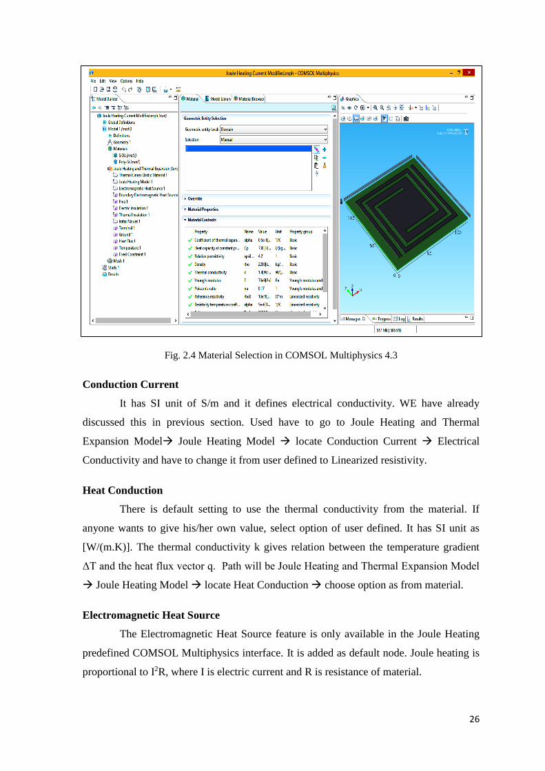
Fig. 2.4 Material Selection in COMSOL Multiphysics 4.3
Conduction Current
It has SI unit of S/m and it defines electrical conductivity. WE have already
discussed this in previous section. Used have to go to Joule Heating and Thermal
Expansion Model Joule Heating Model locate Conduction Current Electrical
Conductivity and have to change it from user defined to Linearized resistivity.
Heat Conduction
There is default setting to use the thermal conductivity from the material. If
anyone wants to give his/her own value, select option of user defined. It has SI unit as
[W/(m.K)]. The thermal conductivity k gives relation between the temperature gradient
ΔT and the heat flux vector q. Path will be Joule Heating and Thermal Expansion Model
Joule Heating Model locate Heat Conduction choose option as from material.
Electromagnetic Heat Source
The Electromagnetic Heat Source feature is only available in the Joule Heating
predefined COMSOL Multiphysics interface. It is added as default node. Joule heating is
proportional to I2R, where I is electric current and R is resistance of material.

27
Initial Values
The initial Values node adds initial values for the temperature T and the electric
potential V that can serve as an initial condition for a transient simulation or as an initial
guess for a non linear solver. If users need to specify more than one set of initial values,
then one can add addition Initial Values features. Generally, temperature is taken as room
temperature (293.15 K) and electric voltage potential is 0V.
Free
Free feature is considered as default boundary condition. That means that there is
no loads and/or no constraint acting on boundary. In micro-heater, this feature is used for
edge.
Ground
This feature is not given directly but we have to choose by right click on Joule
Heating and Thermal Expansion Model and choose electric currents then choose ground
option. In micro-heater, we have to define one end as electric potential and other as
ground.
Fixed Constraint
We have to make fix structure sometimes domain or edges or boundary to
withstand against stress and joule heating. It may change structure. So there is one option
available by right clicking Joule Heating and Thermal Expansion Model Structural
Mechanics Fixed Constraint.
2.5 Conclusion
In this chapter, we have studied and discussed about the COMSOL Multiphysics
4.3 simulation tool with its features and different modules. As we will design and
simulate different micro-heater geometries, this module will helpful to analyzing results
and understand the behavior of micro-heater with respect to its properties.
28
CHAPTER-3
3.1 Sensor design parameters
As already discussed earlier, there is a need of micro-heater for proper detection
of desired gases in any metal oxide gas sensor. Sensing surface heating can be raised by
micro-heater using Joule heating effect, varying thickness of micro-heater geometry or
choosing preferably dielectric for material. In this work, various micro-heater geometries
are analyzed to find optimum solution of micro-heater. Gas sensor made with this
optimized micro-heater should have some basic parameters like, low power consumption,
high sensitivity, low response/recovery time, stability and good lifetime.
Power Consumption
Power consumption is very crucial parameter for any electronic device. It should
have minimum for any device to work that device at low power. For micro-heater, power
consumption can be reduced by decreasing device area and confining heat in particular
geometry. It is necessary to have micro-heater with thermal insulation with rest of
geometry for better heater confinement. The thermal losses in micro-heater are coming
from three sources: heat radiation, transfer of heat from one place to another place
(Convention loss) and conduction from membrane.
Convention loss is dependent on the micro-heater area (it can be reduced) and
radiation loss is not that much (negligible) at 400o C. Micro-heater material should have
low thermal conductivity to reduce heat loss. Parameters like, resistive heating area, total
device area and membrane area should reduce to decrease overall thermal loss.
Lifetime
While voltage potential is applied to micro-heater, there is a thermal stress
induced in the gas sensor (specifically in micro-heater). The stress is generated due to
mismatch in the thermal expansion coefficient in different materials used in gas sensor.
Also when we are achieving high temperature in micro-heater, there is change of crack in
geometry or in sensing film so sensor should have high mechanical stability for better
lifetime.
Response time
This response time can be defined as time required to reaching 67% of the
saturation value. This time is basically corresponding to the response of sensing film. It is

29
necessary to have fast response time (minimum value) where the sensor is placed in
dynamic atmosphere. This time can be decreased by reducing the thinness of membrane
as it reduces thermal mass.
Stability
It is the capability of a gas sensor to provide reproducible results for certain time
duration. This includes retaining to output parameter such as, sensitivity, selectivity and
recovery/response time.
Sensitivity
This is defined as minimum amount of input required to produce specified
output. The sensitivity ‘S’ is expressed below [44,45]:
a g
a
R RS
R
= a
R
R
(3.1)
Where Ra is sensor resistance in air, Rg is resistance in test gas and ΔR is change in the
resistance in presence of reducing gases.
Selectivity
The sensor output may change when it is affected by other environment variables
or parameters. This may appear as noise or unwanted signal. Also the sensor is said to be
non-sensitive. It traditionally defines specificity or selectivity by taking system of n
sensors, each with output value yk
(k= 1, 2…n). The value of partial sensitivity can be
explained as the measured value of output of sensitivity at kth sensor to interfering
quantities or variables Xj as,
ykS
jk Xj
(3.2)

30
3.2 Micro-heater
MEMS Micro-heaters has ability to generate very high temperature at low power
consumption. They also exhibit fast response time. Generally micro-heaters are having a
thin film heater coil or wire which may suspended within silicon for better thermal
isolation. Usually, micro-heaters have platform of Silicon dioxide (SiO2) or Silicon
nitride (SiN). The overall surface temperature can be found by measuring the change in
electrical resistance of micro-heater or they have separate electrodes available to measure
this temperature as shown in Fig.1.3. They are capable to operate at temperature up to
600o C.
The power consumption or heating power (P) can be calculated using formula as
explained below:
2
VP
R (3.3)
Where V is an applied voltage and R is a resistance across two ends of micro-heater.
The value of resistance can be found by mentioned formula for given micro-
heater geometry:
l
Rw h
(3.4)
Where the value of resistivity of material, l is the length, w is the width and h is the
height of micro-heater.
A structure of micro-heater is shown in Fig. 3.1, where 120 x 120 µm2 platform
of Silicon dioxide (SiO2) is used and above it micro-heater is placed.
3.3 Design parameters of micro-heater
The micro-heater design is essential for restrain the temperature distribution
along the active area also to reduce power consumption. To fulfill a desired temperature
distribution, user has to choose proper micro-heater geometry and substrate deliberately.
This is always a key design requirement for many researchers [35,46].

31
Some of the basic requirements must keep in mind those are as follow:
Material used
Uniform temperature distribution over the heater
Mechanical stability
Long life
Micro-heater geometries
Low power consumption
Fig 3.1 A structure of micro-heater
For most effective performance, it is a primary necessity to choose an ideal
material for micro-heater. Mostly, the value of resistivity of material used micro-heater
should be high. Platinum (Pt), Gallium nitride (GaN), Gallium arsenide (GaAs), Titanium
nitride (TiN), DilverP1 (alloy of Ni, Co, Fe), Poly silicon (Poly-Si) and many metal alloys
etc. are widely used materials for micro-heater [47].
It is essential need of micro-heater to have better temperature uniformity for
proper detection of desired gases [26]. So choice of micro-heater geometry which can
distribute temperature equally throughout the sensing surface area without generating any
“hot spot” is desirable.
32
For having long life and mechanical stability of micro-heater, we should
minimize stress and displacement. This is totally dependent on micro-heater material and
its geometry. Also the deformation gradient and thermal expansion of micro-heater must
be lower that will helpful to achieve better results.
Micro-heater geometries plays a vital role for achieve better temperature
uniformity. There are many micro-heater geometries are available and are to investigated
and simulated to attain uniformity.
While choosing micro-heater thickness, one should care about material strength
and heat consumption of the geometry to avoid more heat dissipation loss. Preferred
materials for heat (thermal) isolation are Silicon dioxide (SiO2) and Silicon nitride
(Si3N4). They are used as membrane under the micro-heater though Si3N4 is having more
heat consumption than SiO2 [31].
Low power consumption is most important parameter among all especially for
battery operated sensors. As we have already seen the power consumption equation, by
decreasing width and height of micro-heater geometry, we can increase resistance and
that causes reduction in over all power consumption. So dimensions of micro-heater are
very critical for making power efficient gas sensor.

33
CHAPTER-4
4.1 Selection of micro-heater material
To find micro-heater material, it is necessary to discuss material parameters such
as thermal conductivity, coefficient of thermal expansion and thermal conductivity.
Cooling time or heating time of micro-heater actually dependent on thermal conductivity.
More the value of thermal conductivity of material, higher will be the value of rise time.
Also cooling time is always marginally higher than rise time. This difference is clearly
seen in metals. Variation in object size with temperature change is dependent on
coefficient of thermal expansion. This is measurement of fractional change in size of
structure per degree change in temperature at constant value of pressure. Lastly, electrical
conductivity represents how the temperature increases due to joule heating.
It is always been a challenge to select proper material of micro-heater to achieve
desired temperature requirement for any gas sensor. We have already discussed various
materials available for micro-heater like, Titanium nitride (TiN), Gallium nitride (GaN),
Gallium arsenide (GaAs), DilverP1 (alloy of Ni, Co, Fe), Poly silicon (Poly-Si), Platinum
(Pt), and many metal alloys [47]. Among them Titanium nitride (TiN), Gallium nitride
(GaN), Gallium arsenide (GaAs) are less proffered materials as they have certain major
disadvantages. Dilver P1 is has many advantages such as high yield stress, low thermal
power thermal expansion, low thermal conductivity but it is not that much well-known
material. So for this work, Poly silicon (Poly-Si) and Platinum (Pt) are used as materials
for micro-heater. Poly-Silicon (Poly-Si) has very high resistivity which makes it to more
suitable for micro-heater. Whereas Platinum (Pt) has very high temperature stability
(because melting point is high) so it can easily withstand at very high temperature. So
micro-heater geometries are compared and analyzed using both these materials.
4.2 Micro-heater geometries and their simulation results
Various types of micro-heater geometries are simulated and analyzed using
simulation tool COMSOL Multiphysics 4.3 to achieve basic two requirements namely,
high temperature uniformity and low power consumptions. There are some geometries
like, single meander, double meander, S-shape, fan type, spiral type etc. are chosen by
researchers for making of micro-heater in metal oxide gas sensors [33,37,39].
34
For the simulation purpose, all geometries are made of Poly-Si with micro-heater
geometry height of 2 µm and with 100 x 100 µm2 surface area with platform of SiO2 to
provide thermal insulation to improve temperature profile [48]. And in micro-heater
geometries, one end of micro-heater is having applied voltage of 3.0 V and the other end
is grounded. Comparison has been made for five most desired micro-heater geometries as
mentioned below.
Single meander
Double meander
Fan type
S-shape
Spiral
The purpose of simulation of above geometry is to find the best suitable
geometry which proves better temperature uniformity, so surface temperature will not be
under consideration. Every simulation result represents temperature distribution by
rainbow colors. Where red color area represents maximum temperature and blue area
represents minimum temperature (minimum temperature is defined during boundary
conditions).
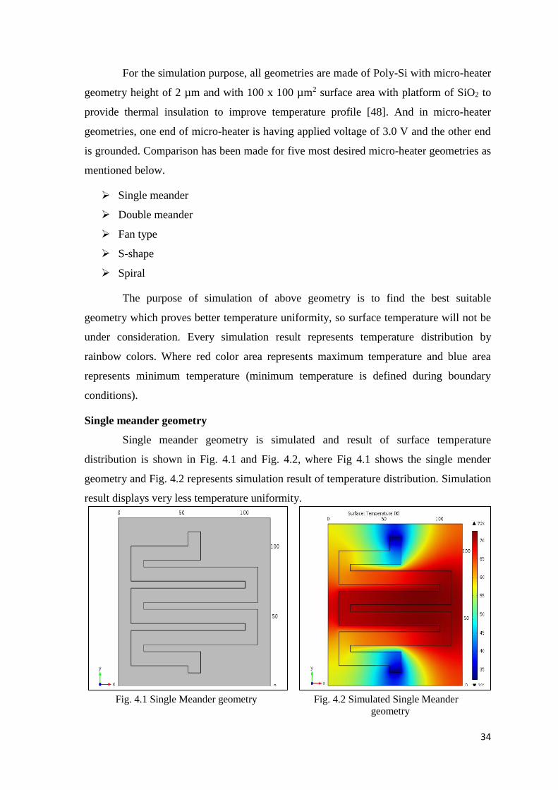
Single meander geometry
Single meander geometry is simulated and result of surface temperature
distribution is shown in Fig. 4.1 and Fig. 4.2, where Fig 4.1 shows the single mender
geometry and Fig. 4.2 represents simulation result of temperature distribution. Simulation
result displays very less temperature uniformity.
Fig. 4.1 Single Meander geometry Fig. 4.2 Simulated Single Meander
geometry

35
Double meander geometry
Single meander and double meander geometry are most studied and researched
geometries among all as they are easy to fabricate and design [39]. Fig 4.3 demonstrates
the single mender geometry and Fig. 4.4 shows simulation result of temperature
distribution. There is a vast improvement in temperature uniformity compare with single
meander geometry.
Fig. 4.3 Double Meander geometry Fig. 4.4 Simulated Double Meander
geometry
Fan type geometry
This type of geometry is very complicated to fabricate though it provides further
improvement in temperature uniformity compare to previous discussed two geometries.
Fig 4.5 is the fan type geometry and Fig. 4.6 represents simulation result.
Fig. 4.5 Fan type geometry Fig. 4.6 Simulated Fan type geometry
36
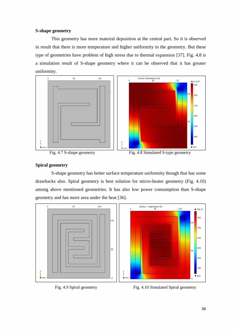
S-shape geometry
This geometry has more material deposition at the central part. So it is observed
in result that there is more temperature and higher uniformity in the geometry. But these
type of geometries have problem of high stress due to thermal expansion [37]. Fig. 4.8 is
a simulation result of S-shape geometry where it can be observed that it has greater
uniformity.
Fig. 4.7 S-shape geometry Fig. 4.8 Simulated S-type geometry
Spiral geometry
S-shape geometry has better surface temperature uniformity though that has some
drawbacks also. Spiral geometry is best solution for micro-heater geometry (Fig. 4.10)
among above mentioned geometries. It has also low power consumption than S-shape
geometry and has more area under the heat [36].
Fig. 4.9 Spiral geometry Fig. 4.10 Simulated Spiral geometry

37
There may be further improvement in result possible by making edges of
geometries curved. This will improve mechanical stability, minimum edge losses and
improvement in maximum surface temperature of micro-heater geometries.
Modified Spiral geometry
There is a further change of temperature uniformity in the same spiral geometry
by merging central area or in other word more deposition in middle portion of geometry.
Geometry will be seen like shown in Fig. 4.11 and micro-heater exhibit more temperature
uniformity then simple spiral geometry (Fig. 4.10).
Fig. 4.11 Modified Spiral geometry Fig. 4.12 Simulated Modified Spiral
geometry
4.3 Conclusion
It is always desirable to have better surface temperature of sensing surface
(which is delivered by micro-heater) for correct detection of certain gases. We have
simulated various micro-heater geometries but S-shape, spiral and modified spiral
geometries provides good surface temperature uniformity. S-shape geometry has high
stress and less stability at high temperature as more deposition in middle portion of
geometry. Also spiral geometry is next available option for micro-heater as it has better
result of temperature uniformity compare to single meander, double meander and fan type
geometries. That can be also improvised by modifying central area of micro-heater. So
we have best available solution of present time micro-heater geometry as modified spiral
geometry.

38
In the next chapter, we will simulate this modified spiral micro-heater geometry
by using Platinum and Poly-Si as micro-heater material. We will see distribution of
current density on the surface, stress on surface, temperature uniformity on surface,
power consumption and micro-heater transient response time for both the cases (Platinum
and Poly-Si). Furthermore, we will discuss effect of height (thickness) variation on power
consumption and temperature of micro-heater. Also there will be discussion on width
variation of micro-heater geometry and its effect on temperature uniformity. All results
will be compared and conclusion will be made based on these.

39
CHAPTER-5
5.1 Parameters consideration under electro – thermal analysis
During the simulation and result analysis, some parameters of micro-heater are
considered as most crucial as they directly affect the performance of gas sensor. They are
mentioned below:
Maximum temperature
Temperature uniformity
Power consumption
Transient temperature response
Transient resistance response of micro-heater
Current density
We have already discussed parameters like, maximum temperature, temperature
uniformity and power consumption so they are not deliberated further in discussion. As
response / recovery time of gas sensor is dependent on sensing surface temperature and
sensing surface temperature is relied on transient temperature response of micro-heater, it
is more crucial to have minimum transient temperature response time of micro-heater.
Due to joule-heating there is variation in resistance of micro-heater. As temperature
increases, value of resistance raises. Also current density represents the distribution of
current on the micro-heater surface (current / area).
5.2 Electro-Thermal analysis
In the previous chapter, various geometries are tried and analyzed for optimum
solution of micro-heater geometry. Then modified spiral geometry is found as optimum
solution which having high resistance value (which is helpful for resistive heating) and
less power consumption. We have already discussed resistive heating (Q) equation in
chapter 2 that is,
2 Q V (5.1)

40
For particular temperature range, the electric conductivity σ is a function of temperature T
according to:
0
10
T T
(5.2)
Where is the temperature coefficient of resistivity, which describes how the resistivity
varies with temperature and 0 is the conductivity at the reference temperature T0. Also
we know that the basic resistance equation including cross sectional area A is,
l
RA
= l
A (5.3)
From above equation, electric conductivity σ and cross sectional area A are inversely
proportional. Also from equation (1), we can conclude that either increases the voltage
gradient of micro-heater two ends (simply increases applied voltage potential of
electrode) or increases the area (thickness or width) of micro-heater. Let us discuss two
cases in which variations in voltage gradient and variations in thickness / area
(thickness * width = area) of micro-heater geometry is analyzed for measure changes in
temperature and power consumption of micro-heater.
Case 1: Change the applied voltage for constant dimensions of micro-heater
geometry.
Case 2: Change the thickness of micro-heater geometry for constant applied voltage.
Modified spiral geometry which is shown in Fig. 5.2.1, is having 2 µm thickness
and it is placed on 120 x 120 µm2 insulating platform of SiO2 having 2 µm thickness. All
dimensions are shown in Fig. 5.2.2. It is analyzed using COMSOL Multiphysics 4.3.
Properties of SiO2 and Poly-Si are defined in Appendix 1. As shown in Fig. 5.2.2, micro-
heater has equal stripe area of 10 µm except the central area of the geometry and central
area is of 40 x 40 µm2.

41
Fig. 5.2.1 3D view of Poly-Si based modified spiral geometry
Fig. 5.2.2 2D view of modified spiral geometry with dimensions
Our aim is to generate surface temperature around 640 - 650K for the analysis of
both the cases.
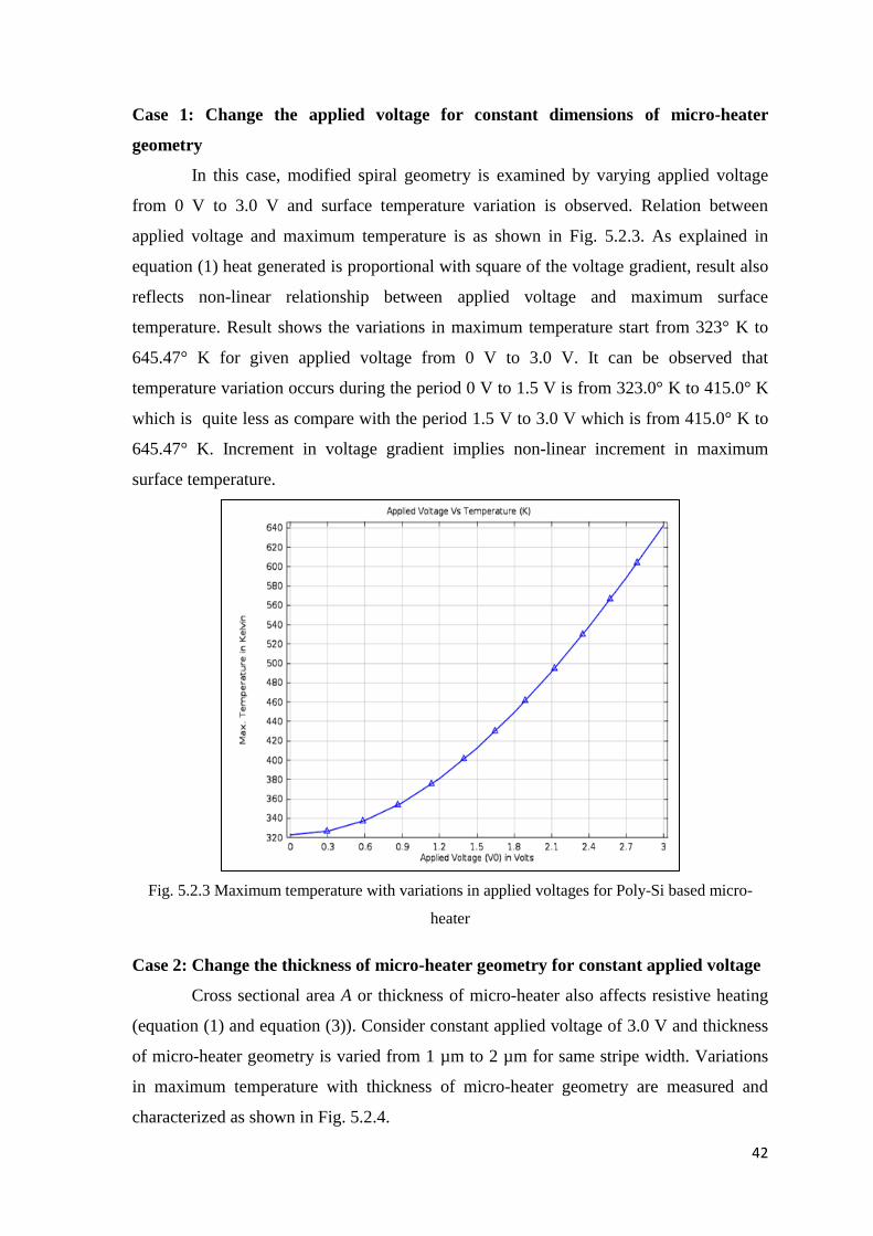
42
Case 1: Change the applied voltage for constant dimensions of micro-heater
geometry
In this case, modified spiral geometry is examined by varying applied voltage
from 0 V to 3.0 V and surface temperature variation is observed. Relation between
applied voltage and maximum temperature is as shown in Fig. 5.2.3. As explained in
equation (1) heat generated is proportional with square of the voltage gradient, result also
reflects non-linear relationship between applied voltage and maximum surface
temperature. Result shows the variations in maximum temperature start from 323° K to
645.47° K for given applied voltage from 0 V to 3.0 V. It can be observed that
temperature variation occurs during the period 0 V to 1.5 V is from 323.0° K to 415.0° K
which is quite less as compare with the period 1.5 V to 3.0 V which is from 415.0° K to
645.47° K. Increment in voltage gradient implies non-linear increment in maximum
surface temperature.
Fig. 5.2.3 Maximum temperature with variations in applied voltages for Poly-Si based micro-
heater
Case 2: Change the thickness of micro-heater geometry for constant applied voltage
Cross sectional area A or thickness of micro-heater also affects resistive heating
(equation (1) and equation (3)). Consider constant applied voltage of 3.0 V and thickness
of micro-heater geometry is varied from 1 µm to 2 µm for same stripe width. Variations
in maximum temperature with thickness of micro-heater geometry are measured and
characterized as shown in Fig. 5.2.4.

43
Fig. 5.2.4 Change in thickness Vs maximum temperature characteristic
It can be analyzed that there is almost linear relation between thickness variation
and maximum temperature of micro-heater. As thickness of micro-heater varies from 1
µm to 2 µm, maximum temperature varies from to 645.47° K with almost equal change
throughout the thickness variation. As thickness increases, resistance of micro-heater
reduces that leads to increase in power consumption. Also transient temperature response
time is also rising with enlargement in thickness of micro-heater. Table 5.2.1
Table 5.2.1 Effect of thickness variation of micro-heater on other parameters for
Poly-Si
Sr.
No.
Thickness of
micro-heater
geometry
Max.
Temp
Power
Consumption
Resistance
value
Transient
temperature
response
µm K mW Ω ms
1. 1.0 570.96 6.55 1375 11.5
2. 1.2 587.56 7.78 1156.8 12.53
3. 1.4 602.9 8.98 998.34 13.56
4. 1.6 618.42 10.21 880.53 14.6
5. 1.8 632.2 11.42 787.41 15.62
6. 2.0 645.47 12.63 713 16.66
From the Table 5.2.1, it is clear that thickness of micro-heater geometry affect
maximum temperature, power consumption, resistance of micro-heater and transient

44
temperature response. Except resistance of micro-heater, all the parameters will increase
with increase in thickness of micro-heater geometry.
5.3 Effect of width variation in micro-heater geometry
We have already understood case 2 where increment in thickness of micro-heater
causes change in parameters. Also we have discussed that heat capacity dependent on
area (i.e. thickness and width). Now consider double meander geometry having 2 µm
thickness of micro-heater geometry and SiO2 based insulating platform of 120 x 120 µm2
and 2 µm thickness.
Fig. 5.3.1 3D view of double meander geometry
Fig. 5.3.2 2D view of double meander geometry with dimensions

45
We are going to change its width and we will analyze the effect on surface
temperature. Fig. 5.3.1 shows double meander geometry and Fig. 5.3.2 shows same
geometry with dimensions.
Now structure widths are varied as shown in Fig. 5.3.3 and Fig. 5.3.4. Simulation
result of double meander geometry and changed width double meander geometry are
compared in Fig. 5.3.5 and Fig. 5.3.6 respectively.
Fig. 5.3.3 3D view of changed width double meander geometry
Fig. 5.3.4 2D view of Poly-Si based changed width double meander geometry with dimensions

46
Fig. 5.3.5 Simulated result for double Fig. 5.3.6 Simulated result for changed
meander geometry width double meander geometry
If we reduce the cross sectional area (width) at which less temperature and
increases area at which we have high temperature better temperature uniformity can be
achieved as shown in Fig. 5.3.5 and Fig. 5.3.6.
5.4 Simulation of Poly-Si based modified spiral geometry
As we have already seen the modified spiral geometry in Fig. 5.2.1, we are going
to applied 3.0 V supply voltage at one electrode of geometry, 2 µm is thickness of
geometry, and SiO2 based insulating platform of 120 x 120 µm2 and 2 µm thickness. We
are trying to find different parameters of this geometry. Fig. 5.4.1 represents surface
temperature response.
Fig. 5.4.1 Simulated Poly-Si based modified spiral geometry
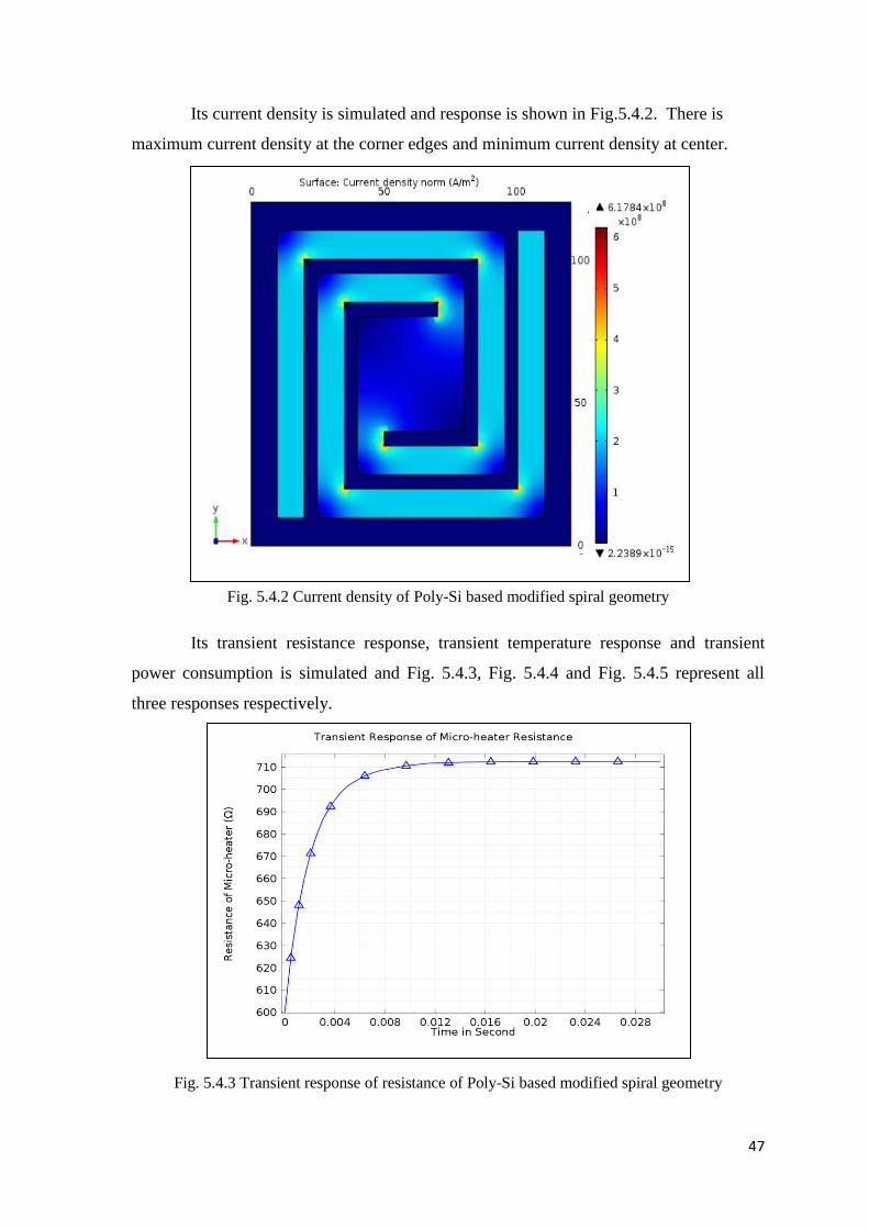
47
Its current density is simulated and response is shown in Fig.5.4.2. There is
maximum current density at the corner edges and minimum current density at center.
Fig. 5.4.2 Current density of Poly-Si based modified spiral geometry
Its transient resistance response, transient temperature response and transient
power consumption is simulated and Fig. 5.4.3, Fig. 5.4.4 and Fig. 5.4.5 represent all
three responses respectively.
Fig. 5.4.3 Transient response of resistance of Poly-Si based modified spiral geometry

48
Fig. 5.4.4 Transient response of power consumption of Poly-Si based modified spiral geometry
Fig. 5.4.5 Transient temperature response of Poly-Si based modified spiral geometry
Now, we will change the geometry and trying to improve results for better
temperature uniformity. So we are changing the width of geometry accordingly.
Fig. 5.4.6 and Fig. 5.4.7 shows changed width geometry for better temperature
uniformity. We will inspect other parameters like, current density, transient resistance
response, transient temperature response and transient power consumption also.

49
Fig. 5.4.6 3D view of Poly-Si based changed width modified spiral geometry
Fig. 5.4.7 2D view with dimensions of Poly-Si based changed width modified spiral geometry

50
After simulation, we have better temperature uniformity on micro-heater
geometry as shown Fig. 5.4.8. After comparison of result Fig. 5.4.1 and Fig. 5.4.8, we can
conclude that after proper width variation, we can improve temperature uniformity.
Fig. 5.4.8 Simulated Poly-Si based changed width modified spiral geometry
Also Fig. 5.4.9, Fig.5.4.10, Fig. 5.4.11 and Fig. 5.4.12 are shown below; they are
responses of current density, transient resistance response, transient temperature response
and transient power consumption respectively.
Fig. 5.4.9 Current density of Poly-Si based changed width modified spiral geometry
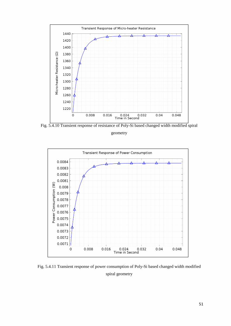
51
Fig. 5.4.10 Transient response of resistance of Poly-Si based changed width modified spiral
geometry
Fig. 5.4.11 Transient response of power consumption of Poly-Si based changed width modified
spiral geometry

52
Fig. 5.4.12 Transient temperature response of Poly-Si based changed width modified spiral
geometry
Results are compared for both the Poly-Si based geometries and shown in Table
5.4.1.
Table 5.4.1 Comparison of parameters of two geometries for Poly-Si
Spiral Geometry with
equal width of 10µm
Spiral Geometry with
unequal width
Max. Surface
Temperature 645.47 °K at 3.0V
572.89 °K at 3.0V
645.47 °K at 3.4662V
Transient Temperature
response time 13 ms 23 ms
Resistance Variation
600.51 Ω to 712.54 Ω (till
temperature reaches 323 °K
to 645.47 °K)
1210.6 Ω to 1433.8 Ω (till
temperature reaches 323 °K to
645.47 °K)
Power Consumption 12.63mW 8.3791mW

53
5.5 Simulation of Platinum based modified spiral geometry
As now, we are known with modified spiral geometry as shown in Fig. 5.2.1. But
in this case, platinum based micro-heater is placed on SiO2 platform of 120 x 120 µm2
surface. Properties of Platinum are defined in Appendix 1. It is observed that around 640-
650o K temperature is achieved at only 0.3V supply. Simulation result is shown in Fig.
5.5.1.
Fig. 5.5.1 Simulated Platinum based modified Spiral geometry
As we have considered two cases in Poly-Si based micro-heater geometry, same
cases are taken for Platinum based geometry.
Case 1: Change the applied voltage for constant dimensions of micro-heater
geometry
In joule heating example, it was discussed that heating is proportional to square
of voltage gradient. Applied voltage is varied from 0 V to 0.3 V for Platinum based
micro-heater and result is analyzed. We can observe that variation from 0 V to 0.15 V,
there is maximum surface temperature variation is from 323o K to 428o K. As voltage
gradient is more from 0.15 V to 0.3 V, we have temperature variation from 428o K to

54
645.47o K. (large temperature variation can be observed). So graph shown in Fig. 5.5.2 is
non-linear.
Fig. 5.5.2 Maximum temperature with variations in applied voltages for Platinum based micro-
heater
Now consider 2nd case where we will observe change in parameter with thickness
variation.
Case 2: Change the thickness of micro-heater geometry for constant applied voltage
Consider modified micro-heater geometry and varied its thickness from 1 µm to
2 µm for constant applied voltage of 0.3V. Fig. 5.5.3 shows response of thickness
variation and maximum surface temperature which is almost linear.

55
Fig. 5.5.3 Change in thickness Vs maximum temperature characteristic
Also Table 5.5.1 represents effect of thickness variation of micro-heater on other
parameters like, maximum temperature of surface, power consumption of micro-heater,
resistance of micro-heater and transient response time. It is observed that with thickness
increases, maximum temperature of surface increases, power consumption increases,
resistance of micro-heater decreases and transient temperature response time increases.
Table 5.5.1 Effect of thickness variation of micro-heater on other parameters for
Platinum
Sr.
No.
Thickness of
micro-heater
geometry
Max.
Temp
Power
Consumption
Resistance
value
Transient
temperature
response
µm K mW Ω ms
1. 1.0 574.71 10 9.02 13.82
2. 1.2 590.76 11.8 7.62 14.31
3. 1.4 606.77 13.52 6.63 14.84
4. 1.6 620.61 15.48 5.88 15.32
5. 1.8 633.1 17.05 5.28 15.8
6. 2.0 645.47 18.83 4.79 16.35
Its current density is simulated and response is shown in Fig.5.5.4. At the corner
edges, we have maximum current density.

56
Fig. 5.5.4 Current density of Platinum based modified spiral geometry
Fig. 5.5.5, Fig. 5.5.6 and Fig. 5.5.7 are represented by transient resistance
response, transient power consumption response and transient temperature response
respectively.
Fig. 5.5.5 Transient response of Platinum based micro-heater resistance

57
Fig. 5.5.6 Transient response of power consumption of Platinum based modified spiral geometry
Fig. 5.5.7 Transient temperature response of Platinum based modified spiral geometry
Now we are changing width of micro-heater for better temperature uniformity as
already seen in Fig. 5.4.6 and Fig. 5.4.7. And simulation result are analyzed for the same
supply voltage of 0.3 V. Fig. 5.5.8 represents surface temperature response of Platinum
based micro-heater.

58
Fig. 5.5.8 Simulated Platinum based changed width micro-heater geometry
It can be observed that maximum surface temperature reduces from 645.47o K to
570.37o K. If we increase applied voltage from 0.3 V to 0.3555 V, we can achieve same
645.47o K. Now consider supply voltage of 0.3555 V then surface density is shown in
Fig. 5.5.9. There is less current density at centre of micro-heater geometry.
Fig. 5.5.9 Current density of Platinum based changed width modified spiral geometry
Also Fig. 5.5.10, Fig. 5.5.11 and Fig. 5.5.12 are represented by transient
resistance response, transient power consumption response and transient temperature
response respectively.
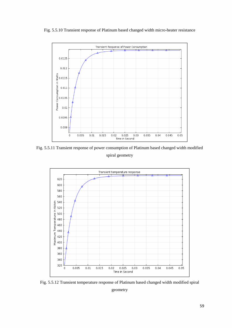
59
Fig. 5.5.10 Transient response of Platinum based changed width micro-heater resistance
Fig. 5.5.11 Transient response of power consumption of Platinum based changed width modified
spiral geometry
Fig. 5.5.12 Transient temperature response of Platinum based changed width modified spiral
geometry

60
Results are compared for both the Platinum based geometries and shown in Table
5.5.2.
Table 5.5.2 Comparison of parameters of two geometries for Platinum
Spiral Geometry with
equal width of 10µm
Spiral Geometry with
unequal width
Max. Surface
Temperature 645.47 °K at 0.3 V
570.37° K at 0.3 V
645.47 °K at 0.3555 V
Transient Temperature
response time 16.4 ms 27 ms
Resistance Variation
3.28 Ω to 4.8 Ω (till
temperature reaches 323 °K
to 645.47 °K)
6.6 Ω to 9.8 Ω (till temperature
reaches 323 °K to 645.47 °K)
Power Consumption 18.83 mW 12.89 mW
Now, parameters comparison of Poly-Si and Platinum based modified spiral
geometry covers in Table 5.5.3 and after changing width of modified spiral geometry are
compared in Table 5.5.4.
Table 5.5.3 Parameters comparison of modified spiral geometry for Poly-Si and
Platinum
Poly-Si based modified
Spiral geometry
Platinum based modified
Spiral geometry
Max. Surface Temperature 645.47° K at 3.0 V 645.47° K at 0.3 V
Transient Temperature
response time 13 ms 16.4 ms
Resistance Variation
600.51 Ω to 712.54 Ω (till
temperature reaches 323 °K
to 645.47 °K)
3.28 Ω to 4.8 Ω (till
temperature reaches 323° K
to 645.47° K)
Power Consumption 12.63mW 18.83 mW

61
Table 5.5.4 Comparison of parameters of modified spiral geometry with changed
width for Poly-Si and Platinum
Poly-Si based modified
Spiral geometry
Platinum based modified
Spiral geometry
Max. Surface
Temperature
572.89 °K at 3.0V
645.47 °K at 3.4662V
570.37° K at 0.3 V
645.47 °K at 0.3555 V
Transient Temperature
response time 23 ms 27 ms
Resistance Variation
1210.6 Ω to 1433.8 Ω (till
temperature reaches 323 °K to
645.47 °K)
6.6 Ω to 9.8 Ω (till
temperature reaches 323 °K to
645.47 °K)
Power Consumption 8.3791mW 12.89 mW
5.6 Conclusion
After simulation of Poly-Si and Platinum based geometry, it is clear that Platinum
consumes more power and has more transient temperature response time to achieve same
temperature which was attained by in Poly-Si based structure. While we need very less
applied voltage in case of Platinum based micro-heater to reach same temperature value
compare with Poly-Si based micro-heater geometry. Though there are some
disadvantages in case of Poly-Si based micro-heater like, less temperature stability and
fabrication difficulty. There are certain drawbacks in case of Platinum based micro-heater
such as, more expensive and less resistivity.

62
CHAPTER-6
6.1 Fabrication steps of MEMS based gas sensor
For design of MEMS based gas sensor, Silicon <100> is used as substrate
material shown in Fig. 6.1.
Fig. 6.1 Silicon wafer <100> as substrate
Its fabrication steps are as followed:
Wafer cleaning
Oxidation
Lithography
Platinum deposition
Silicon nitride deposition (sputtering) and annealing
Back side membrane patterning and Oxide Etching
Silicon etching using TMAH solution
Silicon nitride removal
IDT deposition
Deposition of Sensing layer
6.1.1 Wafer Cleaning
Generally, before using silicon wafer in fabrication process, it should be cleaned
chemically to remove heavy metals, organic films and particulates. There are three
different techniques available for cleaning.
Piranha Cleaning
RCA- 1 Cleaning
RCA-2 Cleaning
For use any one technique, one should switch on the exhaust of chemical hood.
Wear protective gown, goggle, mouth mask, head cap just before starting work on wet
bench.
(A) Piranha Cleaning

63
Piranha solution which is used for cleaning purpose, is made of a mixture
of H2SO4 (sulfuric acid) and H2O2 (hydrogen peroxide). As the mixture is a
strong oxidizing agent, that will clean most of organic matter, also it will
also hydroxylate partially all surfaces (add OH groups) and it is making them
highly hydrophilic (water compatible).
There are many different mixture ratios utilized and all are commonly called
piranha. A typical mixture is 3:1 concentrated H2SO4 (sulfuric acid) to 30%
H2O2 (hydrogen peroxide); other protocols can be used a 4:1 or even 7:1 mixture. A
closely related mixture, sometimes called "base piranha", is a 3:1 mixture of ammonium
hydroxide (NH4OH) with hydrogen peroxide. Piranha solution must be made with great
precautions. It is very corrosive and also an extremely powerful oxidizer. Surfaces must
be carefully cleaned, and totally free of organic solvents before coming into contact with
piranha solution. Piranha solution makes clean by dissolving organic impurities, and a
large amount of impurity will reason violent bubbling also a discharge of gas that can
cause an explosion.
Piranha solution must be prepared by adding H2O2 (hydrogen peroxide) to
H2SO4 (sulfuric acid) very slowly, never vice versa. This process will generate heat. The
resultant heat can increase solution temperatures exceeding 100° C. Before applying any
heat, it must be permissible to cool reasonably. The abrupt raise in temperature can also
lead to violent boiling, or even spraying of the tremendously acidic solution. Explosions
may occur if the peroxide solution concentration is higher than 50% of total solution.
Once the mixture is become stable, it can be further heated to maintain its reactivity. The
hot (often bubbling) solution will clean organic composites off substrates, and oxidize or
hydroxylate most of surfaces. Cleaning usually requires about 10 to 40 minutes, after
which time the substrates can be removed from the solution.
The solution may be mixed before application or directly applied to the material,
applying the sulfuric acid first, followed by the peroxide. Due to the self-decomposition
of hydrogen peroxide, piranha solution should be used freshly prepared. Piranha solution
should not be stored. Immersing the substrate (such as a wafer) into the solution should be
done slowly to prevent thermal shock that may crack the substrate material.
(B) RCA- 1 Cleaning
64
Take 2 quartz beakers, 1 measuring cylinder, wafer holder and wash with DI
(Deionised) water. (DI water plant has been placed just next to the wet bench)
Preparation of RCA-1 solution:
RCA-1 is a solution of Deionised Water (DI H2O): ammonium
hydroxide (NH4OH): H2O2 (hydrogen peroxide) (5:1:1)
(Always add reactive compounds (acid/base) to water)
a.) 200 ml DIH2O
b.) 40 ml NH4OH
c.) 40 ml H2O2
Take 200ml DI water into Cleaned beaker .Add 40ml H2O2 and 40ml NH4OH to
DI water. Once the solution is prepared, keep it on a hot plate. Turn on the hot plate and
set temperature to 150° C. The solution will need to be heated to 80° C. This will take
about 15 minutes. Once solution gets heated up to 80° C, load silicon wafer into wafer
holder and immerse into heated RAC1 solution for 15 minutes. After 15 minutes of
cleaning take out wafers from the solution and rinse with DI water thoroughly for
1minute.
(C) RCA- 2 Cleaning
Preparation of RCA-2 solution:
RCA-2 is a solution of Deionised Water (DI H2O): Hydrochloric acid (HCl):
H2O2 (hydrogen peroxide) (6:1:1)
a) 240 ml DI Water
b) 40 ml H2O2
c) 40 ml HCl
Take 240ml DI water into Cleaned beaker .First Add 40ml H2O2 and then 40ml HCl to DI
water. Once the solution is prepared, keep it on a hot plate. Turn on the hot plate and set
temperature to 150° C. The solution will need to heat to 80° C. This will take about 15
minutes. Once solution gets heated up to 80° C, load silicon wafer into wafer holder and
immerse into heated RAC-2 solution for 15 minutes. After 15 minutes of cleaning take
out wafers from the solution and rinse with DI water thoroughly for 1minute.
The RCA-2 cleaning removes metallic contaminants from the wafer.

65
Preparation of dilute HF (hydrofluoric acid solution):
Measure 200ml of DI water using measuring cylinder and pour into 250 ml
polypropylene beaker and then measure 2ml of HF in a polypropylene measuring cylinder
and add to DI water and mix thoroughly using Teflon rod. Then dip RCA2 cleaned silicon
wafer into dilute HF solution for 15 seconds and finally rinse with DI water for 1min.
Now the wafers are ready for thermal wet oxidation process.
6.1.2 Oxidation
There are four different methods of oxidation as mentioned below:
1. Diffusion oxidation
2. Wet oxidation
3. High pressure oxidation
4. Plasma oxidation
Though all methods are effective but wet oxidation is used for MEMS based gas
sensor fabrication process. Wet oxidation is explained with details as below.
Switch on the mains of thermal wet oxidation furnace to grow 1000 nm oxide
layer. Ramp up furnace temperature to 500° C and pass nitrogen gas (0.5 liter/min) into
the furnace to create inert nitrogen atmosphere. Then load the wafers into furnace and
ramp up furnace temperature from 500° C to 1100° C. Now pass oxygen gas (1 liter/min)
directly into the furnace for 10 minutes for dry oxidation. After 10 minutes stop direct
supply of oxygen gas into the furnace and pass oxygen through the water bubbler
(bubbler temperature should be 97° C) for 3hrs for wet oxidation. After 3hrs stop oxygen
supply and pass nitrogen gas (0.5 liter/min).Ramp down the furnace temperature to 37° C
and unload the wafers. This oxide is used as a hard mask during the Potassium Hydroxide
(KOH) etching process. After this step, we have structure as shown in Fig. 6.2.
Fig. 6.1.2 Structure after wet oxidation
6.1.3 Lithography

66
Top side of oxidized wafer is coated with S1813 Photoresist at 4000rpm for
40secs and prebaked at 125° C temperature for 1minute for top layer pattern transferring
double sided EVG 620 mask aligner was used. The UV bulb is switched on for 10 minute
for stabilization. Mask is loaded according to procedure (guided by software on the
screen)
The parameters set are:
Soft Contact
Constant Dosage - 75mJ/cm2
Wafer is loaded and aligned with the mask
The mask pattern is transferred onto the coated photoresist by UV exposure
The pattern is then developed in a MF26A developer solution for 1min and rinsed with DI
water followed by nitrogen drying.
6.1.3 Top view of mask lay out design of micro-heater with dimension
6.1.4 Platinum deposition
200nm platinum was deposited after lithography process by sputtering method.

67
Fig. 6.1.4 Structure after Platinum deposition
Sputtering parameters:
Plate voltage: 1.5 KV
Incident power: 60w
Reflected power: 25w
Plate current: 60mA
Distance between target and substrate: 5.2cm
Pre sputtering time: 2min
Deposition time: 8min
6.1.5 Silicon nitride deposition (sputtering) and annealing
80nm silicon nitride was deposited as a hard mask for bulk silicon etching.
Sputtering parameters:
Plate voltage: 1.5KV
Incident power: 60W
Reflected power: 20W
Plate current: 60mA
Distance between target and substrate: 6cm
Pre sputtering time: 15min
Deposition time: 15min
Fig. 6.1.5 Structure after Silicon Nitride deposition
After deposition nitride was annealed in a polymer annealing furnace at 700° C
temp for 45 min in nitrogen ambient. Flow rate of nitrogen was 0.5 ltr/min.
6.1.6 Back side membrane patterning and Oxide Etching

68
Back side of oxidized wafer was coated with S1813 Photoresist at 4000rpm for
40secs and prebaked at 125 degree temp for 1min.For membrane pattern was aligned with
respect to top layer pattern by double sided EVG 620 mask aligner.
The UV bulb is switched on for 10 min for stabilization.
Mask is loaded according to procedure (guided by software on the screen)
The parameters set are:
Soft Contact
Constant Dosage - 75mJ/cm2
Wafer is loaded and aligned with the mask
The mask pattern is transferred onto the coated photoresist by UV exposure. The pattern
is then developed in a MF26A developer solution for 1min and rinsed with DI water
followed by nitrogen drying.
Fig. 6.1.6 Structure after membrane patterning and Oxide Etching
6.1.7 Silicon etching using KOH + IPA and TMAH solution
Preparation of 30% KOH solution:
Weigh 105g of 85% pure KOH pellets into 250ml glass beaker and add 195ml of DI
water and stir it thoroughly till KOH pellets dissolves completely. Keep this solution on a
hot plate for heating to 75° C .once after reaching temperature add 50ml of IPA to the
heated KOH solution and immerse wafer into the solution for silicon etching for 2hrs and
30min after 2hrs and 30min etching take out wafer from the solution and wash with DI
water thoroughly and dry with nitrogen.
Etch rate of silicon in KOH+IPA is 50micron/ hour and etch rate of silicon oxide is
150nm / hour.

69
Preparation of 5% TMAH solution:
Take 200ml of DI water in a clean 250ml beaker and then add 40ml of 25%TMAH
solution. Once the solution is prepared, keep it on a hot plate .Turn on the hot plate and
set temperature to 150° C. The solution will need to heat to 75° C. This will take about 15
minutes. Once solution gets heated up to 75° C, add 0.2g of ammonium persulphate salt
to the solution. Load KOH+IPA etched silicon wafer into wafer holder and immerse into
heated TMAH solution for 3 hrs for further silicon etching. Take out sample from the
solution and rinse with DI water followed by methanol.
(Ammonium persulphate should be added at each 15 minutes interval during etching).
Fig. 6.1.7 Structure after Silicon etching using KOH + IPA and TMAH solution
6.1.8 Silicon Nitride Removal
Silicon nitride was etched using 1:3 BHF solution by dipping for 10secs.After etching of
silicon nitride layer wafer was thoroughly rinsed with DI water and dried with nitrogen.
Fig. 6.1.8 Structure after removal of Silicon Nitride
6.1.9 IDT deposition
For deposition of IDT (Interdigitated Electrodes), there is same procedure
followed which is used in micro-heater deposition. Generally, Au or/and Ag materials are
used for IDT. Use of IDT is to detect resistance change of sensing surface.
Fig. 6.1.9 IDT structure for detection of resistance change of sensing surface
6.1.10 Deposition of Sensing Layer

70
On IDT electrodes, sensing surface is deposited. Typically, Tin oxide (SnO2),
Zinc oxide (ZnO), Tungsten trioxide (WO3), Indium tin oxide (ITO), Titanium oxide
(TiO2), Cerium oxide (CeO2) are used for sensing surface.
CHAPTER-7
7.1 Conclusion
In this micro-heater for MEMS based metal oxide gas sensor has been studied in
details. Principle of joule-heating has discussed to understand the working of micro-
heater. Design criteria and design rules have been provided by research methodology and
obtained results for better analysis and better optimization of gas sensor with satisfying
some basic requirements such as, low power consumption, better temperature uniformity
and transient temperature response time with low risk of break and burn through.
Different micro-heater geometries are designed and simulated for finding best suitable
option for gas sensor application. Dimensions of geometry have been varied to achieve
better temperature uniformity. Their characteristics such as power consumption, surface
temperature response, transient resistance response, current density distribution and
transient temperature response time have been studied in details and results are compared.
In Chapter 6, fabrication steps are discussed for implementation of MEMS based metal
oxide gas sensor.
Among the various micro-heater geometries, modified spiral geometry has been
chosen for analysis as it provides better temperature uniformity in all available micro-
heater geometries. Poly-Si and Platinum are the materials used for design and simulation
of micro-heater. Poly-Si and Platinum based micro-heater are analyzed to achieve 640 -
650o K temperature. Poly-Si based micro-heater has achieved this temperature at 3.0 V
applied voltage. Its resistance variation was from 600.51 Ω to 712.54 Ω (till temperature
reaches 323° K to 645.47° K) with transient temperature response time of around 13 ms.
Also power consumption is around 12.63 mW. While in case of Platinum based micro-
heater 640 - 650o K temperature range has been achieved at applied voltage of 0.3 V only.
Variation of resistance is from 3.28 Ω to 4.8 Ω (till temperature reaches 323° K to

71
645.47° K) with transient temperature response time of 16.4 ms. And Power consumption
is of 18.83 mW in case of Platinum based micro-heater.
So After simulation of Poly-Si and Platinum based geometry, it is clear that
Platinum consumes more power and has more transient temperature response time to
achieve same temperature which was attained by in Poly-Si based structure. While we
need very less applied voltage in case of Platinum based micro-heater to reach same
temperature value as of Poly-Si based micro-heater geometry. Though there are some
disadvantages in case of Poly-Si based micro-heater like, less temperature stability and
fabrication difficulty. There are certain drawbacks in case of Platinum based micro-heater
such as, more expensive and less resistivity.
7.2 Future Scope
In future more optimization is possible to make better micro-heater geometry. As
different applications need different micro-heaters, it is more crucial part of micro-heater
design to optimize parameters and to select proper material. Design parameter
optimization can be achieved by varying substrate thickness, dimensions and
modification of micro-heater internal edges. Recently, Dilver P1 (which is composition of
alloy like, Fe, Ni and Co) is considered available option as it consumes less power and
having good resistivity though it generates less temperature compared to Platinum and
Poly-Si.

72
REFERENCE:
[1] M. Mehregany, “Microelectromechanical syatem”, Circuit and Devices Magazine
IEEE, vol. 9, no. 6, pp. 14-22, July 1993.
[2] Stephen D. Senturia, Microsystem Design. London: Kluwer Academic Publishers,
November 2000.
[3] “What is MEMS Technology?,” www.mems-exchange.org [Online]. Available:
https://www.mems-exchange.org/MEMS/what-is.html, [Accessed: 2 June 2014].
[4] An Introduction to MEMS, PRIME Faraday Partnership, Loughborough University,
Loughborough, U.K., 2003.
[5] Zaini Abdul Halim, “Design of Microhotplate Based Gas Sensing System”, Ph.D
Thesis, Electrical & Electronic Engineering Department, Universiti Sains Malaysia, May
2008.
[6] R. Ghodssi and P. Lin, “MEMS Materials and Processes Handbook”, Springer, New
York, London, 2011.
[7] K. Arshak, E. Moore, G.M. Lyons, J. Harris and S. Clifford, “A review of gas sensors
employed in electronic nose applications”. Sensor Review, vol. 24, no. 2, pp.181-198,
November, 2004.
[8] T.C. Pearce, S. S. Schiffman, H.T. Nagle, and J. W. Gardner, Handbook of Machine
Olfaction, Wiley-VCH, Weinheim, 2003.
[9] Frank Ro¨ck, Nicolae Barsan, and Udo Weimar, “Electronic Nose: Current Status and
Future Trends”. Chemical Reviewer, vol. 108, pp. 705-725, August 2008.
[10] Fauzan Khairi Che Harun, Andik Marwintan Jumadi and Nasrul Humaimi
Mahmood, “Carbon black polymer composite gas sensor for electronic nose”,
International Journal of Scientific & Engineering Research, vol. 2, no. 11, November
2011.

73
[11] Alphus D. Wilson 1, and Manuela Baietto, “Applications and Advances in
Electronic-Nose Technologies”, Sensors, vol.9, pp. 5099-5148, June 2009.
[12] Seokheun Choi, Simeng Chen, Yuchao Wang, “ Applications and Technology of
Electronic Nose for Clinical Diagnosis”, Open Journal of Applied Biosensor, vol. 2, pp.
39-50, May 2013.
[13] Paul E. Keller, Lars J. Kangas, Lars H. Liden, Sherif Hashem, Richard T. Kouzes,
“Electronic noses and their applications”, Proceedings of IEEE Northcon/Technical
Applications Conference (TAC’95), Portland, OR, USA, 12 October 1995.
[14] J. W. Gardner, E. L. Hines, and M. Wilkinson, “Application of Artificial Neural
Networks to an Electronic Olfactory System”, Measurement Science and Technology,
vol. 1, pp. 446-451, November 1990.
[15] David Tin Win, “The Electronic Nose – A Big Part of Our Future”, AU J.T., vol. 9,
no. 1, pp. 1-8, July 2005.
[16] K. Wetchakuna, T. Samerjaia, N. Tamaekonga, C. Liewhirana, C. Siriwonga, V.
Kruefua, A. Wisitsoraatb, A. Tuantranontb and S. Phanichphanta, “Semiconducting metal
oxides as sensors for environmentally hazardous gases.”, Sensors and Actuators B,
vol.160, pp. 580– 591, August 2011.
[17] George Preti, Thomas S. Gittelman, Paul B. Staudte, and Preston Luitweiler,
“Letting the nose lead the way: malodorous components in drinking water”, Analytical
Chemistry, vol. 65, no. 15, pp. 699A-702A, August 1993.
[18] T.V. Belysheva, L.P. Bogovtseva, E.A. Kazachkov and N.V. Serebryakova, “Gas-
sensing properties of doped In2O3 films as sensors for NO2 in air”, Journal of Analytical
Chemestry, vol. 58, no. 6, pp. 583–587, 2003.
[19] Kane Jonathan Miller, “Simulation and fabrication of microhotplates for metal oxide gas
sensors”, M.Tech Dissertation, Chemical Department, B.S. University of Louisville, August
2010.
[20] Kraig D. Mitzner, Jason Sternhage and David W. Galipeau, “Development of a
micromachined hazardous gas sensor array”, Sensors and Actuators B, vol. 93, pp.92-99,
2003.

74
[21] Tetsuro Seiyama, Akio Keto, Kiyoshi Jiishi and Masonori Nagatani, “A New
Detector for Gaseous Components Using Semiconductive Thin Films”, Analytical
Chemistry, vol. 34, no.11, pp.1502-1503, October 1962.
[22] H. Meixner and U. Lampe, “Metal oxide sensors”, Sensors and Actuators B, vol. 33,
pp. 198-202, February 1996.
[23] Martin Hausner, Johannes Zacheja and Josef Binder, “Multi-electrode substrate for
selectivity enhancement in air monitoring”, Sensors and Actuators B, vol. 43, pp. 11–17,
April 1997.
[24] Marius Dumitrescu, Cornel Cobianu, Dan Lungu, Dan Dascalu, Adrian Pascu, Spas
Kolev and Albert van den Berg, “Thermal simulation of surface Micromachined
polysilicon hotplates of low power consumption”, IEEE, pp. 83-86, 1998.
[25] S. Semancik, R.E. Cavicchi, M.C. Wheeler, J.E. Tiffani, G.E. Poierier, R.M. Walton,
J.S. Suehle, B. Panchapakesan and D.L. De Voe, “Microhotplate platforms for chemical
sensor research”, Sensors and Actuators B, vol. 77, pp. 579–591, 2001.
[26] Isolde Simon, Nicolae BaÃrsan, Michael Bauer and Udo Weimar, “Micromachined
metal oxide gas sensors: opportunities to improve sensor performance”, Sensors and
Actuators B, vol. 73, pp. 1-26, 2001.
[27] M. Afridi, A. Hefner, D. Berning, C. Ellenwood, A. Varma, B. Jacob and S.
Semancik, “MEMS-based embedded sensor virtual components for system-on-a-chip
(SoC)”, Solid-State Electronics, vol. 48, pp. 1777–1781, 2004.
[28] M. Baroncini, P. Placidi, G.C. Cardinali and A. Scorzoni, “Thermal characterization
of a microheater for micromachined gas sensors”, Sensors and Actuators A, vol. 115, pp.
8–14, 2004.
[29] J. Cerdà Belmonte, J. Puigcorbe, J. Arbiol , A.Vila, J. R. Morante, N. Sabate, I.
Gracia and C. Cane,“ High-temperature low-power performing micro machined
suspended micro-hotplate for gas sensing applications”. Sensors and Actuators B,
vol. 114, pp. 826–835, 2006.
[30] Ching-Liang Dai, Mao-Chen Liu, Fu-Song Chen, Chyan-Chyi Wu and Ming-Wei
Chang, “A nanowire WO3 humidity sensor integrated with micro-heater and inverting
amplifier circuit on chip manufactured using CMOS-MEMS technique”, Sensors and
Actuators B, vol. 123, pp. 896–901, 2007.

75
[31] J. F. Creemer, D. Briand, H. W. Zandbergen, W. van der Vlist, C. R. de Boer, N. F.
de Rooij and P. M. Sarro,“Microhotplates with TiN heaters”, Sensors and Actuators A,
vol. 148, pp. 416–421, 2008.
[32] H. Y. Lee, S. Moon, S. J. Park, J. Lee, K.-H. Park and J. Kim, “Micro- Machined
resistive micro-heaters for high temperature gas sensing applications”, Electronics
Letters, vol. 44, no. 25, 2008.
[33] G. Velmathi, N. Ramshanker and S. Mohan, “2D Simulations and Electro-Thermal
Analysis of Micro-Heater Designs Using COMSOLTM for Gas Sensor Applications”, in
Proceedings of the COMSOL Conference, India, 2010.
[34] Jae-Cheol Shim and Gwiy-Sang Chung, “Fabrication and Characteristics of Pt/ZnO
NO Sensor Integrated SiC Micro Heater”, in Proceedings of IEEE SENSORS Conference,
pp. 350-353, 2010.
[35] M. Gayake, D. Bokdas and S. Gangal, “Simulations of Polymer based Microheater
Operated at Low Voltage”, in Proceedings of the COMSOL Conference, Bangalore,
India, 2011.
[36] Vineet Bansal , Anil Gurjar, Dinesh Kumar and B. Prasad, “3-D Design, Electro-
Thermal Simulation and Geometrical Optimization of spiral Platinum Micro-heaters for
Low Power Gas sensing applications using COMSOLTM”, in Proceedings of the
COMSOL Conference, India, 2011.
[37] Susmita Sinha, Sunipa Roy and C. K. Sarkar, “Design & Electro-Thermal Analysis
of Microheater for Low Temperature MEMS based Gas Sensor”, in Proceedings of
Chennai and Dr.MGR University Second International Conference on Sustainable
Energy and Intelligent System (SEISCON 2011) , Dr. M.G.R. University, Maduravoyal,
Chennai, Tamil Nadu, India, pp. 20-22, July 2011.
[38] Bijoy kantha, Pallavi kar, Saral saha and Subir Kumar sarkar, “Design and Electro-
Thermal Analysis of MEMS based Micro-hotplate for Gas Sensor”, Chennai and Dr.
MGR University Second International Conference on Sustainable Energy and Intelligent
System, 2011.
[39] L. Sujatha, V. S. Selvakumar, S. Aravind, R. Padamapriya and B. Preethi, “Design
and Analysis of Micro-Heaters using COMSOL Multiphysics for MEMS Based Gas
Sensor”, Proceedings COMSOL Conference, India, 2012.

76
[40] Jianhai Sun, Dafu Cui, Lulu Zhang, Xing Chen, Haoyuan Cai and Hui Li,
“Fabrication and characterization of a double-heater based MEMS thermal flow sensor”,
Sensors and Actuators A, vol. 193, pp. 25– 29, 2013.
[41] Introduction to COMSOL Multiphysics users manual, Oct. 2012
[42] Chris Long & Naser Sayma, “Heat Transfer Module”, Venture Publishing AsP,
2009.
[43] Introduction to Structural Mechanics Module users manuals, May 2012.
[44] S. M. Lee, D.C. Dyer and J. W. Gardner, “Design and optimization of a high-
temperature silicon micro-hotplate for nanoporous palladium pellistors”, Microelectronics
Journal, vol. 34, pp.115–126, 2003.
[45] Lie-yi Sheng, Zhenan Tang, Jian Wu, Philip C.H. Chan and Johnny K.O. Sin, “A
low-power CMOS compatible integrated gas sensor using maskless tin oxide sputtering”,
Sensors and Actuators B, vol. 49, pp. 81–87, 1998
[46] Indrajit Singh and S. Mohan, “3D simulation and elecro-thermal analysis of micro-
hotplate design using CoventorWare for MEMS based gas sensor application”,
International conference on smart material structures and systems, pp. 28-30, 2005.
[47] J. Jakovenkoa, T. Lalinsky, M. Drzik, M. Ivanova, G. Vankob and M. Husak, “GaN,
GaAs and Silicon based Micromechanical Free Standing Hot Plates for Gas Sensors”,
Chemistry 1, pp. 804–807, 2009.
[48] V. K. Khanna, Mahanth Prasad, V. K. Dwivedi, Chandra Sekhar, A. C. Pankaj and J.
Basu, “Design and Electro-Thermal Simulation of a Polysilicon micro-heater on
suspended membrane for use in gas sensing”, Indian Journal of Pure and Applied
Physics, vol. 45, pp. 332-335, April 2007.

77
APPENDIX-I
Material properties used in simulation
Sr.
No. Properties SiO2 Poly-Si Platinum
1. Co efficient of thermal
expansion in 1/K 0.5e-6 2.6e6 8.80e6
2. Heat capacity at constant
pressure in J/kg-K 730 678 133
3. Relative permittivity 4.2 4.5 7.0
4. Density in kg/m3 2200 2320 21450
5. Thermal Conductivity in
W/m-K 1.4 34 71.6
6. Young’s modulus in Pa 70e9 160e9 168e9
7. Poisson’s ratio 0.17 0.22 0.38
8. Electrical Resistivity in
Ω-m 10e18 0.00002 10.6e-8

78
LIST OF PUBLICATION
Published:
[1] Palak Bhatt and Anil Arora, “Area effect analysis on surface temperature gradient in
MEMS micro heater for gas sensor applications”, in Proceeding International Conference
on Emerging Technologies in Electronics & Communication (ICETEC-13), pp. 117-119,
Dec. 20-22, 2013.
[2] Palak Bhatt, Manish Deshwal, H. Monga and Anil Arora, “Uniform Temperature
Distribution of MEMS Micro-heater for Efficient MEMS based Gas Sensors”, in
Proceeding 3rd National Conference on Advances in Metrology (AdMet – 2014), Feb.
19-21, 2014.
Communicated:
[1] Palak Bhatt, Himanshu Monga and Anil Arora, “Design and performance analysis of
MEMS micro-heater for uniform temperature platform”, International Journal of
Electronics, June, 2014.