development of metallic microstructure control method · pdf filedevelopment of metallic...
TRANSCRIPT

Development of Metallic Microstructure Control Method by using Nano Plastic Forming
Kohei IBUKI1, Akinori YAMANAKA2 and Masahiko YOSHINO3
1 Department of Mechanical and Control Engineering, Tokyo Institute of Technology, Japan, [email protected] 2 Department of Mechanical and Control Engineering, Tokyo Institute of Technology, Japan,
[email protected], 3 Department of Mechanical and Control Engineering, Tokyo Institute of Technology, Japan, [email protected]
Abstract: In order to control microstructures in metallic materials precisely, we develop a new approach to control the metallic microstructures by using the nano plastic forming which can apply precise strain into the material and exact heat treatment. In this study, we investigate the statically recyrstallized microstructure in a single crystal copper formed by the nano plastic forming. The results show that dislocation cell and subgrain structure are generated by the forming. Furthermore, we can find that the nucleation and growth of the recrystallized grains are occurred from the deformed microstructures. Keywords: Nano Plastic Forming, Microstructure Control, Recrystallization, EBSD, HVEM
1. Introduction
Nano/micro forming technologies have been used to develop various structures, surface patterns and micro mechanical parts of micro/nano devices such as MEMS. The authors have developed the nano plastic forming (NPF) method, which is direct indentation of a wedged-shaped diamond tool, and applied for fabrication of various nano- and micro-surface patterns. By fabricating these surface patterns, we can successfully develop electrical and optical surface functions [1-2].
In this study, we propose a new approach to control metallic microstructures by utilizing the NPF which can apply strain into the material precisely and exact heat treatment. In previous studies, the thermo-mechanical processing which is a combination of macroscopic plastic forming and heat treatment has attracted attention as a way of controlling the microstructures during a manufacturing process. However, since many researchers have focused on the recrystallization in polycrystalline alloy after macroscopic plastic forming such as rolling, thus, it was difficult to reveal the nucleation and growth behaviors of individual recrystallized grain essentially [3-4].
In order to control the recrystallization process precisely, it is well-known that nucleation and growth behaviors of the recrystallized grain must be revealed. For the nucleation mechanism of static recrystallization, although several theories have been proposed, the mechanism based on the abnormal growth of subgrains during annealing is considered as a convincing theory [5-6]; dislocation cell structures formed by severe plastic deformation change to subgrains by recovery during annealing and the subgrains grow large enough to the nuclei of the recrystallized grain due to further annealing. However, the nucleation and growth behaviors of individual recrystallized grain have not been clarified yet.
Therefore, this paper intends to reveal the nucleation
and growth behaviors of an individual recrystallized grain in a single crystal metallic material by the proposed approach with the NPF [7]. Through the experiments, we investigate the plastic deformation behavior and the static rerystallization in a single crystal copper (Cu) as follows. First, change of the crystal orientation by the NPF is analyzed by the electron backscattered diffraction (EBSD) analysis. Also, to clarify the formation of dislocation cell and subgrain structures, which is origin of the nuclei of the recrystallized grain, the high voltage transmission electron microscopy (HVEM) observation of the formed Cu specimen is conducted. Then, the thermal annealing of the formed Cu specimen is carried out to induce the static recrystallization. Furthermore, the nucleation and growth of the individual recrystallized grain are analyzed by using the EBSD. Based on the obtained results, controllability of the recrystallized microstructure is discussed.
2. Experimental method 2.1 Nano plastic forming
Figure 1 illustrates the overall view of NPF equipment used in this study [8]. It has computer-controlled X-Y-Z stages. Feed resolution of those stages is 10nm, and the strokes of X-Y stages and Z stage are 20mm and 40mm, respectively. A diamond tool and a load cell are mounted on the Z stage. The X-Y stages are mounted on the tilt stage whose resolution is 0.015 degrees. The complete process of the forming involving the movement of stages and load measurement are controlled by a computer.
Figure 2 shows a knife edge tool used in this study. It is made of a single crystal diamond. The edge angle is 120 degrees and the width is 1mm. The edge radius is less than 50nm. The sharp knife edge tool was used in this experiment so that large and steep strain distribution can be introduced in the specimen.

Figure 2: Knife edge diamond tool.
In this study, a single crystal copper is used as a work material. Specimens of 11mm × 6mm × 2mm is cut out from an ingot. The upper surface of the specimen is polished to mirror-like finish. The distorted layer is removed by chemical polishing.
Figure 3 shows configuration of the specimen and the tool. The indented surface corresponds to the {111} crystal plane. The longitudinal direction of the tool is set to be parallel to [110] direction of the specimen. The NPF is conducted with indentation loads of 3, 7, 10 and 15N.
Figure 3: Configuration of a single crystal Cu specimen and a knife edge diamond tool. 2.2 Thermal annealing
After the NPF, the formed Cu specimen is annealed in an electric furnace with Argon atmosphere for 2 minutes and 5 minutes. The annealing temperature is set to be 973K which is measured by the thermocouple sheath inserted into the furnace. The temperature of the specimen during the annealing is measured by another thermocouple
sheath which is contacted with a dummy Cu specimen. Immediately after the annealing, the specimen is cooled down by blowing Argon gas. Figure 4 shows the temperature histories of the specimen during the annealing for different annealing temperature and time.
X-Y stages
Z stage Load cell
Diamond tool
Tilt stage
Specimen
Figure 1: NPF equipment.
Figure 4: Temperature histories of the specimen
2.3 HVEM observation To investigate the formation of dislocation cell
structure and the subgrain in the Cu specimen by the NPF, the HVEM observation is conducted. Samples for the HVEM observation are prepared by using focused ion beam (FIB) machining. Before the FIB machining, a protection carbon layer is deposited on the indented groove. Subsequently, to make a 0.5μm thick foil sample containing the groove, two trenches on both side of groove are made with acceleration voltage of 40kV. The foil sample is lifted out and fixed to a mesh by means of a micromanipulator. For the HVEM observation, a Hitachi High-Technologies H1250 operating at 1000kV is used. 2.4 EBSD analysis
To investigate the crystal rotation due to the NPF and the nucleation and growth of the recrystallized grain, distribution of the crystal orientation in the deformed and the annealed Cu specimens is measured by EBSD. The specimens are implanted into the conductive resin and are ground so that cross section of the grooves appears. The cross section of specimens is polished by SiC abrasive paper (#800, #1000, #1200 and #2400) and alumina suspensions whose particle size are 5μm, 1μm and 0.1μm. Finally, it is finished by Chemo-Mechanical-Polishing with colloidal silica with particle size of 0.05μm. Figure 5 shows the finished cross section around the groove.
Figure 5: Picture and SEM image of the cross section of the specimen.
Conductive resin
Copper
ND
RD
TD
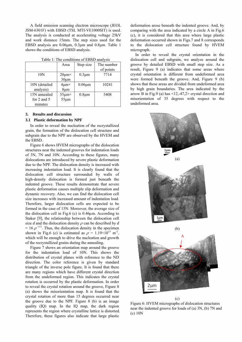
A field emission scanning electron microscope (JEOL JSM-6301F) with EBSD (TSL MTI-VE1000SIT) is used. The analysis is conducted at accelerating voltage 25kV and work distance 15mm. The step sizes used for the EBSD analysis are 0.06μm, 0.3μm and 0.8μm. Table 1 shows the conditions of EBSD analysis.
Table 1: The conditions of EBSD analysis Area Step size The number
of points 10N 20μm×
30μm 0.3μm 7714
10N (detailed analysis)
4μm× 8μm
0.06μm 10241
15N annealed for 2 and 5
minutes
55μm×55μm
0.8μm 5408
3. Results and discussion 3.1 Plastic deformation by NPF
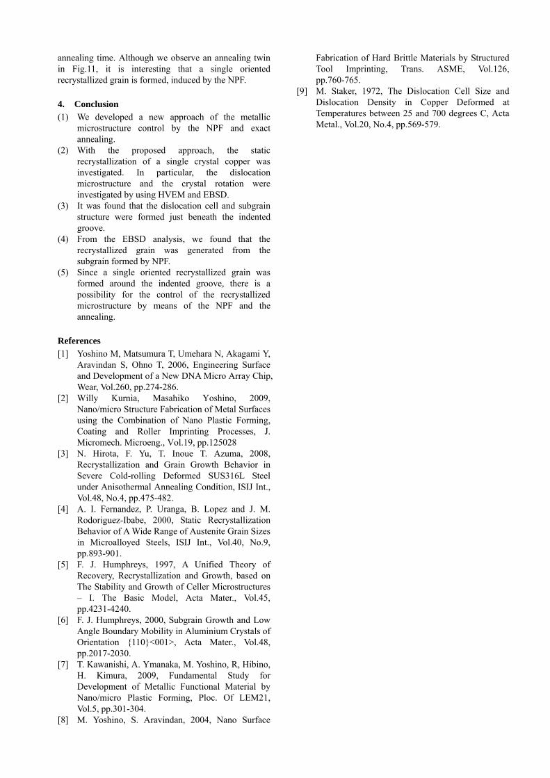
In order to reveal the nucleation of the recrystallized grain, the formation of the dislocation cell structure and subgrain due to the NPF are observed by the HVEM and the EBSD.
Figure 6 shows HVEM micrographs of the dislocation structures near the indented grooves for indentation loads of 3N, 7N and 10N. According to these figures, many dislocations are introduced by severe plastic deformation due to the NPF. The dislocation density is increased with increasing indentation load. It is clearly found that the dislocation cell structure surrounded by walls of high-density dislocation is formed just beneath the indented groove. These results demonstrate that severe plastic deformation causes multiple slip deformation and dynamic recovery. Also, we can find the dislocation cell size increases with increased amount of indentation load. Therefore, larger dislocation cells are expected to be formed in the case of 15N. Moreover, the average size of the dislocation cell in Fig.6 (c) is 0.46μm. According to Staker [9], the relationship between the dislocation cell size d and the dislocation density ρ can be described by d = 16 ρ -1/2. Thus, the dislocation density in the specimen shown in Fig.6 (c) is estimated as ρ = 1.19×10¹⁵ m-2, which will be enough to drive the nucleation and growth of the recrystallized grains during the annealing.
Figure 7 shows an orientation map around the groove for the indentation load of 10N. This shows the distribution of crystal planes with reference to the ND direction. The color reference is given by standard triangle of the inverse pole figure. It is found that there are many regions which have different crystal direction from the undeformed region. This indicates the crystal rotation is occurred by the plastic deformation. In order to reveal the crystal rotation around the groove, Figure 8 (a) shows the misorientation map. It is found that the crystal rotation of more than 15 degrees occurred near the groove due to the NPF. Figure 8 (b) is an image quality (IQ) map. In the IQ map, the dark region represents the region where crystalline lattice is distorted. Therefore, these figures also indicate that large plastic
deformation arose beneath the indented groove. And, by comparing with the area indicated by a circle A in Fig.6 (c), it is considered that this area where large plastic deformation occurred shown in Figs.7 and 8 corresponds to the dislocation cell structure found by HVEM micrograph.
In order to reveal the crystal orientation in the dislocation cell and subgrain, we analyze around the groove by detailed EBSD with small step size. As a result, Figure 9 (a) indicates that some areas where crystal orientation is different from undeformed area were formed beneath the groove. And, Figure 9 (b) shows that these areas are divided from undeformed area by high grain boundaries. The area indicated by the arrow B in Fig.9 (a) has <12,-47,2> crystal direction and misorientation of 35 degrees with respect to the undeformed area.
(a)
(b)
(c)
Figure 6: HVEM micrographs of dislocation structures near the indented groove for loads of (a) 3N, (b) 7N and (c) 10N
A

Figure 7: Crystal orientation map for indantation load of 10N.
(a) (b) Figure 8: (a) Misorientation map and (b) IQ map for
indantation load of 10N.
(a) (b) Figure 9: (a) Crystal orientation map and (b) IQ map with misorientation between subgrains beneath the indented groove.
In addition, since the diameter of the area B is 0.780μm, it is considered that the area B can contain some dislocation cells and this area corresponds to the subgrain which consists of the multiple dislocation cells.
In the recrystallization process by the annealing, it is
known that the dislocation cells in the subgrain unite each other and become a nucleus of recrystallized grain. The size of the subgrain which was observed in this study is close to the size of nucleus observed in general. Therefore we can predict that the subgrain like the area A becomes the nucleus of the recrystallized grain and it grows up.
[111]
[100] [101]
(a) (b) Figure 10: (a) Crystal orientation and (b) IQ maps in the specimen indented with the load of 15N and annealed for 2 minutes.
(a) (b) Figure 11: (a) Crystal orientation and (b) IQ maps in the specimen indented with the load of 15N and annealed for 5 minutes. 3.2 Static recrystallization
In order to investigate the nucleation and subsequent growth of the recystallized grain, EBSD analysis of the annealed specimens is conducted. Figure 10 shows the crystal orientation map in the specimen indented with the forming load of 15N and annealed for 2 minutes. It can be clearly shown that a recrystallized grain is formed near the indented groove. This recrystallized grain will nucleate and grow from the subgrain structure during the annealing. As shown in Fig.10 (b), since the value of IQ in the recrystallized grain is higher than that in the undeformed area, therefore, the recrystallized grain does not contain dislocations. From these results, it can be confirmed that the growth of the recrystallized grain is driven by the stored energy of the dislocation cell.
Figure 11 shows the distribution of crystal orientation in the specimen indented with the load of 15N and annealed for 5 minutes. Comparing the size of the recrystallized grain shown in Fig.10 with that in Fig.11, the recrystallized grain grows up with increasing
B
annealing time. Although we observe an annealing twin in Fig.11, it is interesting that a single oriented recrystallized grain is formed, induced by the NPF. 4. Conclusion (1) We developed a new approach of the metallic
microstructure control by the NPF and exact annealing.
(2) With the proposed approach, the static recrystallization of a single crystal copper was investigated. In particular, the dislocation microstructure and the crystal rotation were investigated by using HVEM and EBSD.
(3) It was found that the dislocation cell and subgrain structure were formed just beneath the indented groove.
(4) From the EBSD analysis, we found that the recrystallized grain was generated from the subgrain formed by NPF.
(5) Since a single oriented recrystallized grain was formed around the indented groove, there is a possibility for the control of the recrystallized microstructure by means of the NPF and the annealing.
References [1] Yoshino M, Matsumura T, Umehara N, Akagami Y,
Aravindan S, Ohno T, 2006, Engineering Surface and Development of a New DNA Micro Array Chip, Wear, Vol.260, pp.274-286.
[2] Willy Kurnia, Masahiko Yoshino, 2009, Nano/micro Structure Fabrication of Metal Surfaces using the Combination of Nano Plastic Forming, Coating and Roller Imprinting Processes, J. Micromech. Microeng., Vol.19, pp.125028
[3] N. Hirota, F. Yu, T. Inoue T. Azuma, 2008, Recrystallization and Grain Growth Behavior in Severe Cold-rolling Deformed SUS316L Steel under Anisothermal Annealing Condition, ISIJ Int., Vol.48, No.4, pp.475-482.
[4] A. I. Fernandez, P. Uranga, B. Lopez and J. M. Rodoriguez-Ibabe, 2000, Static Recrystallization Behavior of A Wide Range of Austenite Grain Sizes in Microalloyed Steels, ISIJ Int., Vol.40, No.9, pp.893-901.
[5] F. J. Humphreys, 1997, A Unified Theory of Recovery, Recrystallization and Growth, based on The Stability and Growth of Celler Microstructures – I. The Basic Model, Acta Mater., Vol.45, pp.4231-4240.
[6] F. J. Humphreys, 2000, Subgrain Growth and Low Angle Boundary Mobility in Aluminium Crystals of Orientation {110}<001>, Acta Mater., Vol.48, pp.2017-2030.
[7] T. Kawanishi, A. Ymanaka, M. Yoshino, R, Hibino, H. Kimura, 2009, Fundamental Study for Development of Metallic Functional Material by Nano/micro Plastic Forming, Ploc. Of LEM21, Vol.5, pp.301-304.
[8] M. Yoshino, S. Aravindan, 2004, Nano Surface
Fabrication of Hard Brittle Materials by Structured Tool Imprinting, Trans. ASME, Vol.126, pp.760-765.
[9] M. Staker, 1972, The Dislocation Cell Size and Dislocation Density in Copper Deformed at Temperatures between 25 and 700 degrees C, Acta Metal., Vol.20, No.4, pp.569-579.