detailed analysis of a multi-pulse statcom · simulations using the emtdc/pscad. ... statcom employ...
TRANSCRIPT

Detailed analysis of a multi-pulse STATCOM
Ricardo Dávalos Marín

2
AbstractThe rapid development of power electronics technology provides opportunities
to develop new power equipment to improve the performance of the actual powersystems. During the last decade, a number of control devices called ”FlexibleAC Transmission Systems” (FACTS) technology have been proposed and imple-mented. FACTS devices can be used for power flow control, loop-flow control,voltage regulation, enhancement of transient stability and damping of power os-cillations. FACTS devices can be used as a series controller, shunt controllers orby a combination of both.
Since the early 1970s high power, line-commutated thyristors in conjunctionwith capacitors and reactors have been employed in various circuit configurationsto produce variable output such as the shunt connected static VAR compensators(SVC) and the series connected thyristor controlled series capacitor (TCSC), basedon the traditional thyristor-switched capacitors (TSC) and thyristor-controlled re-actors (TCR), which have been widely used for the AC voltage regulation in powersystems by controlling the injection of reactive power. With the advent of highpower gate turn-off thyristor (GTO) and other power semiconductors with an in-ternal turn-off capability as the insulated gate bipolar transistor (IGBT), a newgeneration of power electronic equipment has been implemented in switching con-verter circuits, the voltage source inverters (VSI), to generate and absorb reactivepower without the use of AC capacitor or reactor banks.
The new generation and most dominant converters needed in FACTS con-trollers such as the static synchronous compensator (STATCOM), the static syn-chronous series compensator (SSSC) and by the combination of both the UnifiedPower Flow Controller (UPFC) are based on the voltage-source inverters (VSI).
This work presents the detailed analysis to deduce the expressions for the AC(phase currents and output voltage) and DC signals (capacitor current and voltage)of 6-, 12-, 24-, and 48-pulse VSI-STATCOM. The expressions obtained allowto estimate an appropriate DC capacitor value. Based on a switching model, astate-space representation in the dq-reference frame is deduced. The accuracy ofthe results are validated by comparison the analytical results along with digitalsimulations using the EMTDC/PSCAD.
The relevance of such studies is to exhibit the detailed STATCOM operation,not found commonly in the literature, emphasising assumptions and limitationswhen the dq0 model is used to carry out dynamic studies in large power systems.

ContentsContents . . . . . . . . . . . . . . . . . . . . . . . . . . . . . . . . . . . . . . . . . . . . . . . . . . . . I
List of figures . . . . . . . . . . . . . . . . . . . . . . . . . . . . . . . . . . . . . . . . . . . . . . III
1 Introduction . . . . . . . . . . . . . . . . . . . . . . . . . . . . . . . . . . . . . . . . . . . . . 11.1 Multi-pulse converter configuration . . . . . . . . . . . . . . . . . . . . . . . 41.2 Multi-level converter configuration . . . . . . . . . . . . . . . . . . . . . . . . 51.3 Pulse Width Modulation (PWM) . . . . . . . . . . . . . . . . . . . . . . . . . 71.4 Objetives . . . . . . . . . . . . . . . . . . . . . . . . . . . . . . . . . . . . . . . . . . . 7
References . . . . . . . . . . . . . . . . . . . . . . . . . . . . . . . . . . . . . . . . . . . . . . . . . . . . . . . . . . . 9
2 Analysis of a STATCOM based on 6- and 12-pulses VSI . . . . . . . . . . . 112.1 Introduction . . . . . . . . . . . . . . . . . . . . . . . . . . . . . . . . . . . . . . . . . 112.2 Voltage source-inverter (VSI) . . . . . . . . . . . . . . . . . . . . . . . . . . . . 12
2.2.1 Harmonic analysis . . . . . . . . . . . . . . . . . . . . . . . . . . . . . . . . . . . . . 152.3 Static synchronous compensator (STATCOM) based on
six-pulse VSI . . . . . . . . . . . . . . . . . . . . . . . . . . . . . . . . . . . . . . 202.3.1 Reactive power exchange . . . . . . . . . . . . . . . . . . . . . . . . . . . . . . . 22
Analysis of the AC current signals . . . . . . . . . . . . . . . . . . . 23Conduction period transistors and diodes . . . . . . . . . . . . . 27Capacitor current . . . . . . . . . . . . . . . . . . . . . . . . . . . . . . . . . . 28DC capacitor voltage. . . . . . . . . . . . . . . . . . . . . . . . . . . . . . . 30
2.3.2 Reactive and active power exchange . . . . . . . . . . . . . . . . . . . . . . 32Capacitor current . . . . . . . . . . . . . . . . . . . . . . . . . . . . . . . . . . 36
2.4 12-pulse converter . . . . . . . . . . . . . . . . . . . . . . . . . . . . . . . . . . . . 382.4.1 AC current signals . . . . . . . . . . . . . . . . . . . . . . . . . . . . . . . . . . . . . 44
Six-pulse AC current . . . . . . . . . . . . . . . . . . . . . . . . . . . . . . . 482.4.2 Capacitor current . . . . . . . . . . . . . . . . . . . . . . . . . . . . . . . . . . . . . . 522.4.3 DC capacitor voltage . . . . . . . . . . . . . . . . . . . . . . . . . . . . . . . . . . . 542.4.4 PSCAD/EMTDC Simulations . . . . . . . . . . . . . . . . . . . . . . . . . . . 55
2.5 Conclusions . . . . . . . . . . . . . . . . . . . . . . . . . . . . . . . . . . . . . . . . . 57
References . . . . . . . . . . . . . . . . . . . . . . . . . . . . . . . . . . . . . . . . . . . . . . . . . . . . . . . . . . 58
3 24- and 48-pulse STATCOM operation . . . . . . . . . . . . . . . . . . . . . . . . 59
I

3.1 24-pulse operation . . . . . . . . . . . . . . . . . . . . . . . . . . . . . . . . . . . . 593.1.1 24-pulse voltage . . . . . . . . . . . . . . . . . . . . . . . . . . . . . . . . . . . . . . . 593.1.2 Magnetic interface . . . . . . . . . . . . . . . . . . . . . . . . . . . . . . . . . . . . . 633.1.3 AC current signals . . . . . . . . . . . . . . . . . . . . . . . . . . . . . . . . . . . . . 633.1.4 Capacitor current . . . . . . . . . . . . . . . . . . . . . . . . . . . . . . . . . . . . . . 663.1.5 DC capacitor voltage . . . . . . . . . . . . . . . . . . . . . . . . . . . . . . . . . . . 68
3.2 48-pulse operation . . . . . . . . . . . . . . . . . . . . . . . . . . . . . . . . . . . . 703.2.1 48-pulse voltage . . . . . . . . . . . . . . . . . . . . . . . . . . . . . . . . . . . . . . . 713.2.2 AC current signals . . . . . . . . . . . . . . . . . . . . . . . . . . . . . . . . . . . . . 753.2.3 Capacitor current . . . . . . . . . . . . . . . . . . . . . . . . . . . . . . . . . . . . . . 763.2.4 DC capacitor voltage . . . . . . . . . . . . . . . . . . . . . . . . . . . . . . . . . . . 77
3.3 Digital simulations . . . . . . . . . . . . . . . . . . . . . . . . . . . . . . . . . . . . 793.4 Conclusions . . . . . . . . . . . . . . . . . . . . . . . . . . . . . . . . . . . . . . . . . 80
References . . . . . . . . . . . . . . . . . . . . . . . . . . . . . . . . . . . . . . . . . . . . . . . . . . . . . . . . . . 85
4 STATCOM Modelling . . . . . . . . . . . . . . . . . . . . . . . . . . . . . . . . . . . . . 864.1 Switching functions model . . . . . . . . . . . . . . . . . . . . . . . . . . . . . . 86
4.1.1 12-pulse converter . . . . . . . . . . . . . . . . . . . . . . . . . . . . . . . . . . . . . 904.2 STATCOM model at fundamental frequency . . . . . . . . . . . . . . . . 92
4.2.1 12-pulse converter . . . . . . . . . . . . . . . . . . . . . . . . . . . . . . . . . . . . . 984.2.2 24-pulse converter . . . . . . . . . . . . . . . . . . . . . . . . . . . . . . . . . . . . . 994.2.3 48-pulse converter . . . . . . . . . . . . . . . . . . . . . . . . . . . . . . . . . . . . 100
4.3 dq0 Reference frame model . . . . . . . . . . . . . . . . . . . . . . . . . . . . 1014.4 Conclusions . . . . . . . . . . . . . . . . . . . . . . . . . . . . . . . . . . . . . . . . 103
References . . . . . . . . . . . . . . . . . . . . . . . . . . . . . . . . . . . . . . . . . . . . . . . . . . . . . . . . . 108Conclusions . . . . . . . . . . . . . . . . . . . . . . . . . . . . . . . . . . . . . . . . . . . . . . . 109Future work . . . . . . . . . . . . . . . . . . . . . . . . . . . . . . . . . . . . . . . . . . . . . . . 111
II

List of figures1.1 One-line diagram of a STATCOM . . . . . . . . . . . . . . . . . . . . . . . . 2
1.2 Three phase converter . . . . . . . . . . . . . . . . . . . . . . . . . . . . . . . . . 4
1.3 Multi-pulse staircase voltage waveform . . . . . . . . . . . . . . . . . . . . 5
1.4 Five-level voltage source inverter . . . . . . . . . . . . . . . . . . . . . . . . . 6
1.5 Single-phase three level Chain circuit . . . . . . . . . . . . . . . . . . . . . 6
2.1 Simple voltage sourced-inverter (two level-pole) . . . . . . . . . . . . . 11
2.2 Six-pulse VSI with a resistive load . . . . . . . . . . . . . . . . . . . . . . . . 12
2.3 Firing control signals . . . . . . . . . . . . . . . . . . . . . . . . . . . . . . . . . . 13
2.4 Line-to-line voltage waveform . . . . . . . . . . . . . . . . . . . . . . . . . . . 14
2.5 Equivalent circuit for the sequence 1-5-6 . . . . . . . . . . . . . . . . . . . 14
2.6 Equivalent circuit for the sequence 1-2-6 . . . . . . . . . . . . . . . . . . . 15
2.7 Equivalent circuit for the sequence 1-2-3 . . . . . . . . . . . . . . . . . . . 16
2.8 Line-to-neutral voltage waveform . . . . . . . . . . . . . . . . . . . . . . . . 16
2.9 vab(t) voltage Fourier spectrum . . . . . . . . . . . . . . . . . . . . . . . . . . 19
2.10 0.5 inductive power factor load conduction period . . . . . . . . . . . 20
2.11 0.8660 inductive power factor load conduction period . . . . . . . . . 21
2.12 Inductive load conduction period . . . . . . . . . . . . . . . . . . . . . . . . 21
2.13 Six-pulse VSI-STATCOM . . . . . . . . . . . . . . . . . . . . . . . . . . . . . . 22
2.14 Phase relationship between the inductor voltage VL and thefundamental curren Ia1 . . . . . . . . . . . . . . . . . . . . . . . . . . . . . . . . 24
2.15 Relationship between DC voltage, fundamental andharmonics current . . . . . . . . . . . . . . . . . . . . . . . . . . . . . . . . . . . . 24
2.16 AC system voltage and voltage compensator van(t) . . . . . . . . . . . 25
III
2.17 AC current waveform . . . . . . . . . . . . . . . . . . . . . . . . . . . . . . . . . 27
2.18 Q1 andD1 conduction period . . . . . . . . . . . . . . . . . . . . . . . . . . . 29
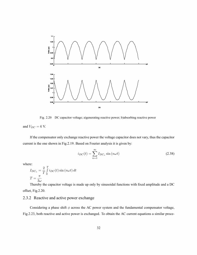
2.19 Capacitor current; a)generating reactive power; b)absorbingreactive power . . . . . . . . . . . . . . . . . . . . . . . . . . . . . . . . . . . . . . . 31
2.20 DC capacitor voltage; a)generating reactive power;b)absorbing reactive power . . . . . . . . . . . . . . . . . . . . . . . . . . . . . 32
2.21 Voltage waveforms with a finite DC capacitor . . . . . . . . . . . . . . . 33
2.22 Capacitor current and DC capacitor voltage waveform . . . . . . . . 33
2.23 AC system voltage and compensator voltage; van(t) . . . . . . . . . . 34
2.24 AC current waveform with φ = 15o . . . . . . . . . . . . . . . . . . . . . . . 36
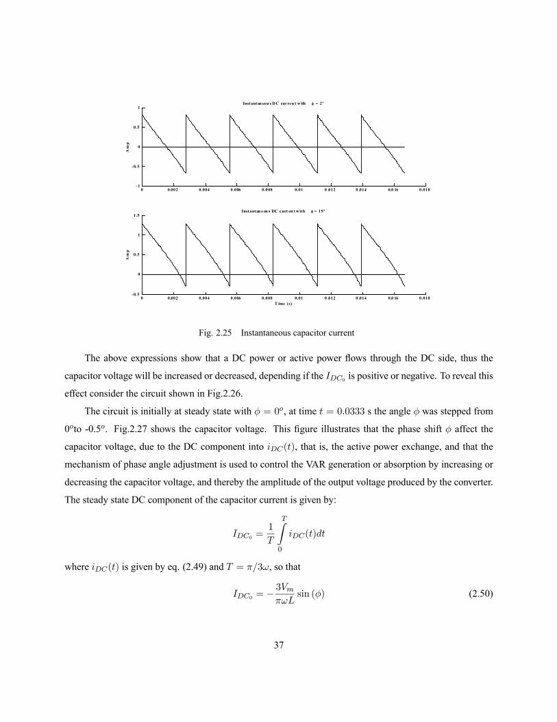
2.25 Instantaneous capacitor current . . . . . . . . . . . . . . . . . . . . . . . . . 37
2.26 Test circuit . . . . . . . . . . . . . . . . . . . . . . . . . . . . . . . . . . . . . . . . . . 38
2.27 Instantaneous capacitor voltage . . . . . . . . . . . . . . . . . . . . . . . . . . 39
2.28 AC instantaneous current with: a)φ = 0o;b)φ = −0.5o . . . . . . . . 39
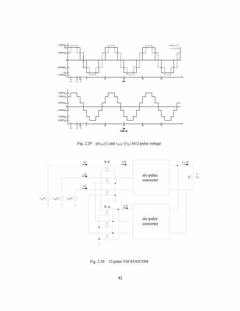
2.29 a)vab(t) and vabY (t)2; b)12-pulse voltage . . . . . . . . . . . . . . . . . . . 42
2.30 12-pulse VSI-STATCOM . . . . . . . . . . . . . . . . . . . . . . . . . . . . . . . 42
2.31 12-pulse STATCOM line-to-neutral voltages . . . . . . . . . . . . . . . . 43
2.32 vab(t)12 voltage Fourier spectrum . . . . . . . . . . . . . . . . . . . . . . . . 45
2.33 Phasorial diagram . . . . . . . . . . . . . . . . . . . . . . . . . . . . . . . . . . . . 45
2.34 Relationship between the DC voltage and the fundamentaland harmonics current . . . . . . . . . . . . . . . . . . . . . . . . . . . . . . . . . 46
2.35 AC system voltage and fundamental voltage compensatorvan(t) . . . . . . . . . . . . . . . . . . . . . . . . . . . . . . . . . . . . . . . . . . . . . . 46
2.36 AC current waveform, ia(t) . . . . . . . . . . . . . . . . . . . . . . . . . . . . . 50
2.37 AC current of each six-pulse VSI . . . . . . . . . . . . . . . . . . . . . . . . . 51
2.38 Q1 andD1 currents . . . . . . . . . . . . . . . . . . . . . . . . . . . . . . . . . . . 51
IV

2.39 First converter capacitor current; a)generating reactivepower; b)absorbing reactive power . . . . . . . . . . . . . . . . . . . . . . . 53
2.40 Second converter capacitor current; a)generating reactivepower; b)absorbing reactive power . . . . . . . . . . . . . . . . . . . . . . . 53
2.41 Capacitor current; a)generating; b)absorbing reactivepower . . . . . . . . . . . . . . . . . . . . . . . . . . . . . . . . . . . . . . . . . . . . . . 54
2.42 DC capacitor voltage; a)generating; b)absorbing reactivepower . . . . . . . . . . . . . . . . . . . . . . . . . . . . . . . . . . . . . . . . . . . . . . 55
2.43 a)12-pulse AC current ia(t); b)12-pulse line-to-line voltagevab(t) . . . . . . . . . . . . . . . . . . . . . . . . . . . . . . . . . . . . . . . . . . . . . . 56
2.44 Capacitor current and DC capacitor voltage waveform . . . . . . . . 56
3.1 24-pulse voltage . . . . . . . . . . . . . . . . . . . . . . . . . . . . . . . . . . . . . . 62
3.2 24-pulse voltage Fourier spectrum . . . . . . . . . . . . . . . . . . . . . . . . 62
3.3 24-pulse STATCOM . . . . . . . . . . . . . . . . . . . . . . . . . . . . . . . . . . 64
3.4 12-pulse grounded transformer with PST on leading andlagging configuration . . . . . . . . . . . . . . . . . . . . . . . . . . . . . . . . . . 65
3.5 Phasor diagram of the phase-shifting mechanism . . . . . . . . . . . . 65
3.6 AC current waveform, ia(t) . . . . . . . . . . . . . . . . . . . . . . . . . . . . . 67
3.7 Phasorial diagram . . . . . . . . . . . . . . . . . . . . . . . . . . . . . . . . . . . . 67
3.8 Capacitor current; a)generating reactive power; b)absorbingreactive power . . . . . . . . . . . . . . . . . . . . . . . . . . . . . . . . . . . . . . . 69
3.9 DC capacitor voltage; a)generating reactive power;b)absorbing reactive power . . . . . . . . . . . . . . . . . . . . . . . . . . . . . 70
3.10 48-pulse STATCOM . . . . . . . . . . . . . . . . . . . . . . . . . . . . . . . . . . 72
3.11 48-pulse voltage . . . . . . . . . . . . . . . . . . . . . . . . . . . . . . . . . . . . . . 75
3.12 48-pulse voltage Fourier spectrum . . . . . . . . . . . . . . . . . . . . . . . . 76
3.13 AC current waveform, ia(t) . . . . . . . . . . . . . . . . . . . . . . . . . . . . . 77
3.14 Capacitor current; a)generating reactive power; b)absorbing
V

reactive power . . . . . . . . . . . . . . . . . . . . . . . . . . . . . . . . . . . . . . . 78
3.15 Capacitor voltage; a)generating reactive power; b)absorbingreactive power . . . . . . . . . . . . . . . . . . . . . . . . . . . . . . . . . . . . . . . 79
3.16 24-pulse behaviour with a fixed VDC value . . . . . . . . . . . . . . . . . 81
3.17 24-pulse behaviour with a finite DC capacitor . . . . . . . . . . . . . . . 82
3.18 48-pulse behaviour with fixed VDC value . . . . . . . . . . . . . . . . . . . 83
3.19 48-pulse behaviour with a finite DC capacitor . . . . . . . . . . . . . . . 84
4.1 Six-pulse VSI-STATCOM . . . . . . . . . . . . . . . . . . . . . . . . . . . . . . 87
4.2 phase ’a’ arm . . . . . . . . . . . . . . . . . . . . . . . . . . . . . . . . . . . . . . . . 88
4.3 Six-pulse behaviour . . . . . . . . . . . . . . . . . . . . . . . . . . . . . . . . . . . 93
4.4 12-pulse behaviour . . . . . . . . . . . . . . . . . . . . . . . . . . . . . . . . . . . . 94
4.5 24-pulse behaviour . . . . . . . . . . . . . . . . . . . . . . . . . . . . . . . . . . . . 95
4.6 48-pulse behaviour . . . . . . . . . . . . . . . . . . . . . . . . . . . . . . . . . . . . 96
4.7 Phase current; a)Switching model; b)model at fundamentalfrequency. . . . . . . . . . . . . . . . . . . . . . . . . . . . . . . . . . . . . . . . . . . 104
4.8 id and iq current . . . . . . . . . . . . . . . . . . . . . . . . . . . . . . . . . . . . . 105
4.9 Capacitor voltage . . . . . . . . . . . . . . . . . . . . . . . . . . . . . . . . . . . . 106
VI

Chapter 1Introduction
In recent years, voltage stability and control are increasingly becoming a limiting factor in the planning
and operation of some power systems, mainly in longitudinal ones. However, a variety of considerations
constrains the construction of new transmission lines. This has been reflected in the necessity to maximise
the use of existing transmission facilities. On steady state, bus voltages must be controlled on a specified
range. A suitable voltage and reactive power control allows to obtain important benefits in the power systems
operation such as the reduction of voltage gradients, the efficient transmission capacities utilisation and the
increase of stability margins. By different control means and operating techniques, the voltage control task
in transmission levels can be got; some solution technologies can involve a series voltage injection, or a
shunt reactive current injection in strategic sites of the power system. When a disturbance occurs, changes
in the voltage system are presented and the restoration to the reference values depends on the dynamic
response of the excitation systems and the control devices employed.
In the last decade commercial availability of Gate Turn-Off thyristor (GTO) devices with high power
handling capability, and the advancement of other types of power-semiconductor devices such as IGBT’s
have led to the development of controllable reactive power sources utilising electronic switching converter
technology [1]. These technologies additionally offer considerable advantages over the existing ones in
terms of space reductions and performance. The GTO thyristors enable the design of solid-state shunt
reactive compensation equipment based upon switching converter technology. This concept was used to
create a flexible shunt reactive compensation device named Static Synchronous Compensator (STATCOM)
due to similar operating characteristics to that of a synchronous compensator but without the mechanical
inertia.
The advent of Flexible AC Transmission Systems (FACTS) is giving rise to a new family of power
electronic equipment emerging for controlling and optimising the performance of power system, e.g. STAT-
COM, SSSC and UPFC. The use of voltage-source inverter (VSI) has been widely accepted as the next
generation of reactive power controllers of power system to replace the conventional VAR compensation,
such as the thyristor-switched capacitor (TSC) and thyristor controlled reactors (TCR).
1
DC-ACSwitchingconverter
System bus VAC
CouplingTransformer
Transformer leakageinductor
Vs
VDC
C
I
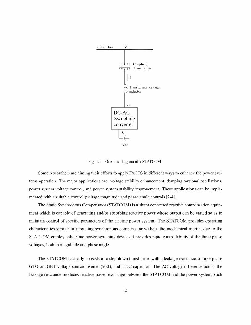
Fig. 1.1 One-line diagram of a STATCOM
Some researchers are aiming their efforts to apply FACTS in different ways to enhance the power sys-
tems operation. The major applications are: voltage stability enhancement, damping torsional oscillations,
power system voltage control, and power system stability improvement. These applications can be imple-
mented with a suitable control (voltage magnitude and phase angle control) [2-4].
The Static Synchronous Compensator (STATCOM) is a shunt connected reactive compensation equip-
ment which is capable of generating and/or absorbing reactive power whose output can be varied so as to
maintain control of specific parameters of the electric power system. The STATCOM provides operating
characteristics similar to a rotating synchronous compensator without the mechanical inertia, due to the
STATCOM employ solid state power switching devices it provides rapid controllability of the three phase
voltages, both in magnitude and phase angle.
The STATCOM basically consists of a step-down transformer with a leakage reactance, a three-phase
GTO or IGBT voltage source inverter (VSI), and a DC capacitor. The AC voltage difference across the
leakage reactance produces reactive power exchange between the STATCOM and the power system, such
2

that the AC voltage at the bus bar can be regulated to improve the voltage profile of the power system, which
is the primary duty of the STATCOM. However, for instance, a secondary damping function can be added
into the STATCOM for enhancing power system oscillation stability [4]. The basic voltage-source inverter
representation for reactive power generation is shown schematically in Fig.1.1.
The principle of STATCOM operation is as follows. The VSI generates a controllable AC voltage
source behind the leakage reactance. This voltage is compared with the AC bus voltage system; when the
AC bus voltage magnitude is above that of the VSI voltage magnitude, the AC system sees the STATCOM
as an inductance connected to its terminals. Otherwise, if the VSI voltage magnitude is above that of the
AC bus voltage magnitude, the AC system sees the STATCOM as a capacitance connected to its terminals.
If the voltage magnitudes are equal, the reactive power exchange is zero. If the STATCOM has a DC source
or energy storage device on its DC side, it can supply real power to the power system. This can be achieved
adjusting the phase angle of the STATCOM terminals and the phase angle of the AC power system. When
the phase angle of the AC power system leads the VSI phase angle, the STATCOM absorbs real power from
the AC system; if the phase angle of the AC power system lags the VSI phase angle, the STATCOM supplies
real power to AC system [5-7].
Typical applications of STATCOM are:
• effective voltage regulation and control.
• reduction of temporary overvoltages.
• improvement of steady-state power transfer capacity.
• improvement of transient stability margin.
• damping of power system oscillations.
• damping of subsynchronous power system oscillations.
• flicker control.
• Power quality improvement.
• distribution system applications.
The voltage source-converter or inverter (VSC or VSI) is the building block of a STATCOM and other
FACTS devices. A very simple inverter produces a square voltage waveform as it switches the direct voltage
source on and off. The basic objective of a VSI is to produce a sinusoidal AC voltage with minimal harmonic
distortion from a DC voltage. Three basic techniques are used for reducing harmonics in the converter output
3

Q1
Q4
Q3 Q5
Q6 Q2
D1 D3 D5
D1 D6 D2
a b c
g1 g3 g5
g4 g6 g2
Fig. 1.2 Three phase converter
voltage. Harmonic neutralisation using magnetic coupling (multi-pulse converter configurations), harmonic
reduction using multi-level converter configurations and the pulse-width modulation (PWM).
1.1 Multi-pulse converter configuration
Multi-pulse operation is achieved, by connecting identical three-phase bridges, Fig. 1.2, to transformers
which have outputs that are phase-displaced with respect to one another. Star and delta-connected windings
have a relative 30ophase shift and a 6-pulse converter bridge connected to each transformer will give an
overall 12-pulse operation eliminating 5th and 7th harmonics. This principle can be extended to 24- and
48-pulse operation summing at the primary windings the transformed outputs of several 6-pulse converters
(4 for 24-pulse and 8 for 48-pulse operation). The harmonic cancellation is carried out into the transformer
secondary windings.
The basic issue in structuring a high-power, multi-pulse converter is the complexity of the magnetic
structure that is needed.
The converter operation is carried out applying low frequency (usually line frequency) firing pulse to
the power switches. Due to the low switching frequency, only about one third of the converter losses are due
to the switching losses, the remaining two thirds are due to the magnetic interface (conduction losses) [1].
A typical multi-pulse waveform is depicted in Fig.1.3.
4

0 0 . 0 0 5 0 . 0 1 0 .0 1 5 0 . 0 2 0 . 0 2 5 0 . 0 3 0 .0 3 5- 4
- 3
- 2
- 1
0
1
2
3
4
Ti m e ( s )
Vo
lts
Fig. 1.3 Multi-pulse staircase voltage waveform
1.2 Multi-level converter configuration
The multi-level inverters synthesize a staircase voltage wave, Fig.1.3, from several levels of DC voltage
sources, obtained from capacitor voltage source. As the number of levels increases, the synthesized staircase
wave approaches the sinusoidal wave resulting in reduced harmonic distortion. Fig.1.4 shows a single-phase
five level voltage source-inverter, this converter is more complex and requires the DC voltage source to be
split or centre-tapped in order to provide a zero voltage reference [8,9].
The fundamental magnitude and the harmonic spectrum are controlled varying the switching angles, α.
The fundamental voltage component can also be changed by keeping α constant and changing VDC .
Alternative forms of multi-level converters is the chain circuit [ 10,11], in which several converter
bridges, each with its own source capacitor, are connected in series as illustrated in Fig.1.5. This topology
is simpler than that presented in Fig.1.4 due to it does not include diodes-clamp and flying capacitors.
The main advantage of the multi-level inverter circuits is their ability to produce quasi-harmonic neu-
tralised output voltage waveforms without magnetic waveform summation circuits. This advantage is offset
by the complexity and size of the DC capacitor, and/or the need for additional power circuit components,
e.g. power diodes, and control functions, e.g. DC voltage equalisation.
5

2VDC
2VDC
2VDC
2VDC
2VDC
2VDC
2VDC
2VDC
Neutral
Vout
2VDC
2VDC
DCVDCV
α1α2
Fig. 1.4 Five-level voltage source inverter
Vout
Neutral
Fig. 1.5 Single-phase three level Chain circuit
6

1.3 Pulse Width Modulation (PWM)
In multi-pulse and multi-level converters, there is only one turn-on, turn-off per device per cycle. An-
other approach is to have multiple pulses per half-cycle, and then vary the width of the pulses to vary the
amplitude of the AC voltage. The pulse width modulation (PWM) technique is commonly employed to
generate high quality output waveforms by relatively low power converter used in variable frequency AC
motor drives and distribution applications [12-14]. With this technique, the output of each converter pole is
switched several times during a fundamental cycle between the positive and negative terminals of the DC
source.
PWM requires a considerable increase in the number switch operations (high switching frequency);
thereby it generally increases the switching losses of the converter [1,5,6]. However, the always increasing
switching frequency of modern solid-state power switches could made possible the use of PWM in high
power applications [15, 16].
Among the various VSI topologies the multi-pulse configurations and the multi-level configuration have
become popular for advanced Static VAR compensation applications. In these configurations the switching
frequency can be kept low in order to minimise device stresses switching losses and electromagnetic inter-
ference [8]. Some commercials STATCOM installed are: The STATCOM installed in Japan in 1991 uses
eight six-pulse VSI, each of 10 MVA rating, connected to a main transformer resulting in 48-pulse STAT-
COM. A 100 MVA 48-pulse STATCOM was installed in 1995 for the Tennessee Valley Authority (TVA) at
the Sullivan Substation in North-Eastern Tennessee [17]. Another application in high power system of the
multi-pulse VSI is in the 160 MVA UPFC installed at the Inez substation of the American Electric Power
(AEP) in Kentucky USA, this is based on two identical 48-pulse VSI.
1.4 Objetives
The STATCOM and other FACTS devices have been widely studied by analytical models but the phys-
ical functionality is unknown for a lot of power researches. The objective of this doctoral work is to present,
analyse and experimentally verify the operation of a multi-pulse-base on three-phase STATCOM.
To accomplish the objective, the following research tasks are performed:
• Present the detailed analysis of 6-, 12-, 24- and 48-pulse-VSI STATCOMThis part presents the relevant details of the voltage source-inverter (VSI), the building block of a STAT-
7

COM and other FACTS devices. A detailed analysis is carried out to deduce the expressions for the AC(phase currents and output voltage) and DC signals (capacitor current and voltage). The analysis allowsto understand how the power exchanged is achieved using a DC capacitor as a DC source, the operatingmodes, and the control voltage.
• STATCOM modelling.Based on a switching model, a state-space representation in the dq-reference frame is deduced. Themodel is used to calculate the control parameters.
• STATCOM designA 12-pulse-VSI STATCOM is designed and simulated using the EMTDC/PSCAD.
• STATCOM laboratory prototype.Using the theoretical analysis and simulations an IGBT-12-pulse-VSI STATCOM will be developed toexperimentally verify the operation of a three-phase STATCOM.
8

References[1] CIGRE, ”Static Synchronous Compensator”, working group 14.19, September 1998.
[2] Z. Yang, C. Shen, L. Zhang, M. L. Crow, ”Integration of a STATCOM and Battery Energy Storage”,
IEEE Trans. on Power System, Vol. 16, no. 2, May 2001, pp. 254-260.
[3] L. Chun, J. Qirong, X. Jianxin, ”Investigation of Voltage Regulation Stability of Static Synchronous
Compensator in power system”, IEEE Power Engineering Society, Proceedings of the Winter Meet-
ing 2000, IEEE Vol. 4, pp. 2642-2647.
[4] H. F. Wang, ”Applications of damping torque analysis to StatCom control”, Electrical Power and
Energy Systems, Vol. 22, 2000, pp. 197-204.
[5] Narain G. Hingorani, Laszlo Gyugyi, ”Understanding FACTS”, IEEE Press 2000.
[6] Yong Hua Song, Allan T. Johns, ”Flexible AC transmission systems FACTS”, IEE Power and Energy
Series 30, 1999.
[7] Zhiping Yang, ”Integration of battery energy storage with flexible AC transmission system devices”,
Ph. D. Thesis, University fo Missouri-Rolla, 2000.
[8] Ekanayake, J. B., Jenkins, N., ”A three-level advanced Static VAR Compensator”, IEEE Trans. on
Power Delivery, Vol. 11, no. 1, pp. 540-545.
[9] C. J. Hatziadoniu, F. E: Chalkiadakis, ”A 12-pulse Static Synchronous Compensator for the distribu-
tion system employing the 3-Level GTO-Inverter”, IEEE Trans. on Power Delivery, Vol. 12, no. 4,
October 1997, pp. 1830-1835.
[10] Krshnat V. Patil, ”Dynamic Compensation of Electrical Power Systems Using a New BVSI-STATCOM”,
Ph. D. Thesis, University of Wester Ontario, London Ontario, Canada, March 1999.
[11] B. Han, S. Back, H. Kim, G. Karady, ”Dynamic Characteristic Analysis of SSSC bases on multibrige
inverter”, IEEE Trans. on Power Delivery, Vol. 17, no. 2, April 2002, pp. 623-629.
[12] J. G. Kassakian, M. F. Schlecht, G. C. Verghese, ”Principles of power electronics”, Addison-Wesley,
1992.
[13] N. Mohan, T. M. Undeland, W. P. Robbins, ”Power Electronics: Converters, Applications, and
Desing”, John Wiley and Sons, 1995.
9

[14] Olimpo Anaya-Lara, E. Acha, ”Modeling and Analysis of Custom Power Systems by PSCAD/EMTDC”,
IEEE Trans. on Power Delivery, Vol. 17, no.1, January 2002, pp. 266-272.
[15] Pablo García Gonzalez, Aurerio García Cerrada, ”Control System for a PWM-Based STATCOM”,
IEEE Trans. on Power Delivery, Vol. 15, no. 4, October 2002, pp. 1252-1257.
[16] G. Venkataramanan, B. K. Johnson, ”Pulse Width Modulated series compensator”, IEE Proc.- Gener.
Transm. Distrib., Vol 149, no. 1, January 2002, pp. 71-75.
[17] C. Schuder, M. Gernhardt, E. Stacey, T. Lemark, L. Gyugyi, T. W. Cese, A. Edris, ”Operation of
±100MVAR TVA-STATCON”, IEEE Trans. on Power Delivery, Vol. 12, no. 4, October 1997.
10
Chapter 2Analysis of a STATCOM based on 6- and 12-pulsesVSI
2.1 Introduction
This chapter presents the detailed analysis of a six and twelve-pulse VSI-STATCOM. The analysis
allows to understand how the power exchanged is achieved using a capacitor as a DC source, the operating
modes, the control voltage, and to give us an important insight into the comprehension of higher pulse
arrangements. To validate the accuracy of the equations encountered digital simulations will be presented.
The VSI is analysed as a linear network with a topology that changes depending on the state of the six
(ideal) switching devices. The analysis exploits the fact that the system is piecewise linear; consequently,
over each interval during which the switches do not change their state, the circuit equations may be solved
using standard linear techniques.
Fig. 2.1 Simple voltage sourced-inverter (two level-pole)
The voltage-sourced converter or inverter (VSC or VSI) is presently considered the best candidate for
the implementation of a high power STATCOM and other FACTS devices based on VSI such as the UPFC
and the SSSC, and all existing and planned new installations known are based on this approach [1]. A two-
11
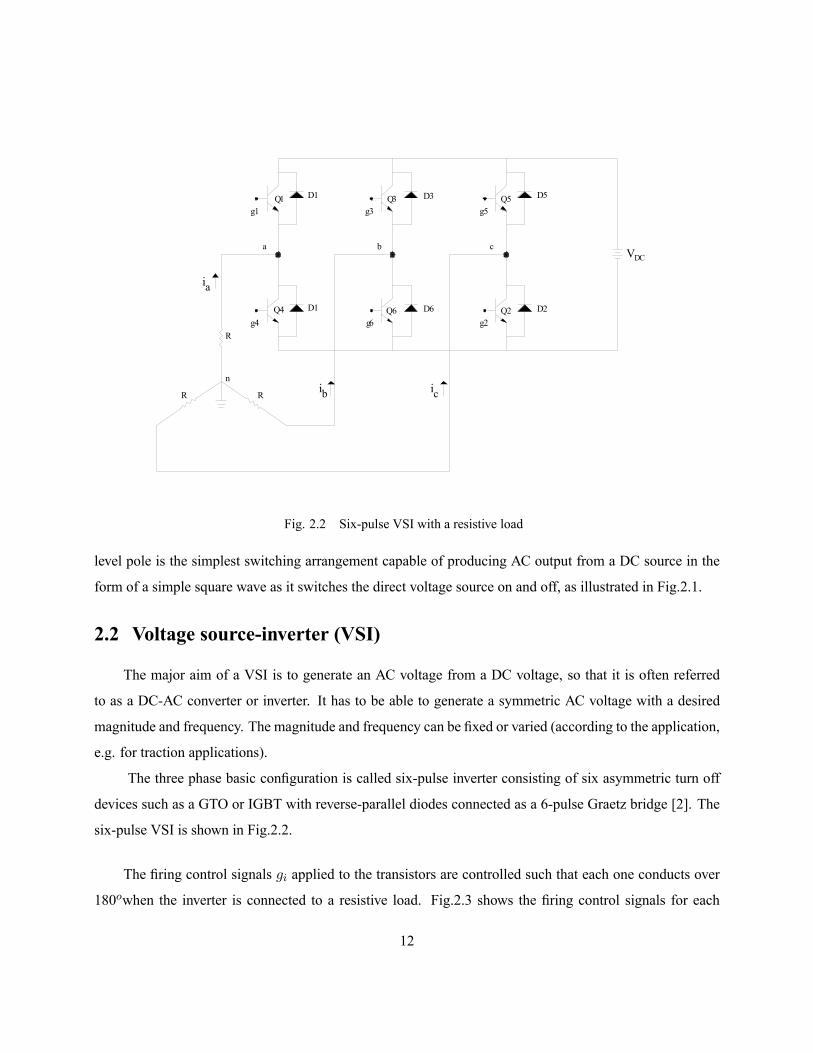
Q1
Q4
Q3 Q5
Q6 Q2
D1 D3 D5
D1 D6 D2
R
RR
n
a b c
g1 g3 g5
g4 g6 g2
ia
ib ic
VDC
Fig. 2.2 Six-pulse VSI with a resistive load
level pole is the simplest switching arrangement capable of producing AC output from a DC source in the
form of a simple square wave as it switches the direct voltage source on and off, as illustrated in Fig.2.1.
2.2 Voltage source-inverter (VSI)
The major aim of a VSI is to generate an AC voltage from a DC voltage, so that it is often referred
to as a DC-AC converter or inverter. It has to be able to generate a symmetric AC voltage with a desired
magnitude and frequency. The magnitude and frequency can be fixed or varied (according to the application,
e.g. for traction applications).
The three phase basic configuration is called six-pulse inverter consisting of six asymmetric turn off
devices such as a GTO or IGBT with reverse-parallel diodes connected as a 6-pulse Graetz bridge [2]. The
six-pulse VSI is shown in Fig.2.2.
The firing control signals gi applied to the transistors are controlled such that each one conducts over
180owhen the inverter is connected to a resistive load. Fig.2.3 shows the firing control signals for each
12
0
0
g1
0
0
g2
0
0
g3
0
0
g4
0
0
g5
0
0
g6
ωt
ωt
ωt
ωt
ωt
ωt
3π
32π π π2 π3 π4 π5
Fig. 2.3 Firing control signals
transistor. The inverter can be seen as the combination of three single-phase inverters where each phase
leg produces an output phase shifted by ±120owith respect to the outputs of the other two legs. The firing
control signals are shifted by 60ofrom each other.
The switching sequence shown in Fig.2.3 generates the line-to-line voltages vab(t), vbc(t) and vca(t)
illustrated in Fig.2.4. In this figure it is noticed that these line-to-line voltages have 120opulse width with
peak voltage magnitude of VDC . For each 60ointerval three different operating modes exists [3]; in the first
half cycle the operating sequence is 1-5-6 (Fig.2.5), 1-2-6 (Fig.2.6) and 1-2-3 (Fig.2.7). In order to obtain
the line-to-neutral voltages the corresponding different operating modes will be analysed.
Sequence 1-5-6; 0 ≤ ωt ≤ π/3
van = vcn =1
3VDC
vbn = −23VDC
Sequence 1-2-6; π/3 ≤ ωt ≤ 2π/3van =
2
3VDC
13
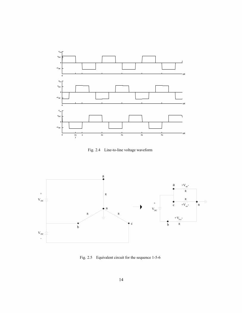
0
0
0
0
0
0
ωt
ωt
ωt
va b
vbc
vca
vDC
-vDC
vDC
-vDC
-vDC
vDC
32π π π2 π3 π4 π5
Fig. 2.4 Line-to-line voltage waveform
R
RR
a
bc
n
Rb
R
c
R
a
n
+
VDC
VDC
+
+
VDC
+Vb n-
+Vcn-
+Van-
Fig. 2.5 Equivalent circuit for the sequence 1-5-6
14

R
RR
a
bc
n
R
R
c
R
n
b
a
+
VDC
+
VDC
+Van-
+Vcn-
+Vbn -
VDC
+
Fig. 2.6 Equivalent circuit for the sequence 1-2-6
vbn = vcn = −13VDC
Sequence 1-2-3; 2π/3 ≤ ωt ≤ π
van = vbn =1
3VDC
vcn = −23VDC
The following three operating modes are obtained in a similar way, and they are the negative of those
shown previously. Fig.2.8 depicts the line-to-neutral voltages van(t), vbn(t) and vcn(t). The synchronisation
and frequency of the generated voltages depend directly on the frequency and synchronisation of the firing
control signals and not on the load type. The peak magnitude voltage depends on the DC voltage.
2.2.1 Harmonic analysis
The harmonic content of the line-to-line and line-to-neutral voltages can be obtained applying a Fourier
analysis to the waveforms shown in Fig.2.4 and Fig.2.8. Half-odd wave symmetry is obtained if vab(t)
voltage is lagged 30o, therefore the instantaneous value of vab(t) based on Fourier analysis is given by
vab(t) =∞Xn=1
Vabn sin³nωt+
π
6n´
(2.1)
15

R
RR
a
bc
n
aR
R
R
nb
c
+
VDC
+
VDC
+
VDC
+Van -
+Vb n-
+Vcn-
Fig. 2.7 Equivalent circuit for the sequence 1-2-3
0
0
0
0
0
0
ωt
ωt
ωt
3π
32π π π2 π3 π4 π5
van
vbn
vcn
DCV32
DCV32
DCV32
DCV31
DCV31
DCV31
DCV31−
DCV31−
DCV31−
DCV32−
DCV32−
DCV32−
0
0
0
0
0
0
ωt
ωt
ωt
3π
32π π π2 π3 π4 π5
van
vbn
vcn
DCV32
DCV32
DCV32
DCV31
DCV31
DCV31
DCV31−
DCV31−
DCV31−
DCV32−
DCV32−
DCV32−
Fig. 2.8 Line-to-neutral voltage waveform
16

where:
Vabn =4
T
5π/6Zπ/6
VDC sin (nωt) dωt (2.2)
T = 2π
so that
Vabn =2
nπVDC
µcos³π6n´− cos
µ5π
6n
¶¶(2.3)
From eq. (2.3) it is worth to note that only the 6r ± 1 (n = 6r ± 1) terms exist, where r is any positive
integer, that is, n = 1th, 5th, 7th, 11th, 13th, ..., therefore eq. (2.3) can be reduced to
Vabn =4
nπVDC cos
³π6n´∀n = 6r ± 1, r = 0, 1, 2, ... (2.4)
Eqns. (2.5) and (2.6) give rise to the fundamental and harmonic components of the line-to-line voltages,
Vab1 = 1.1026VDC peak; Vab1 = 0.7797VDC RMS (2.5)
Vabn =1.1026
nVDC peak; Vabn =
0.7797
nVDC RMS (2.6)
Finally, voltage vab(t) is expressed by eq. (2.7). Voltages vbc(t) and vca(t) have a similar pattern except
phase shifted by 120oand 240o, respectively, from vab(t).
vab(t) =4
πVDC
∞Xn
1
ncos³π6n´sin³nωt+
π
6n´
(2.7)
vbc(t) =4
πVDC
∞Xn
1
ncos³π6n´sin³nωt− π
2n´
(2.8)
vca(t) =4
πVDC
∞Xn
1
ncos³π6n´sin
µnωt− 7π
6n
¶(2.9)
∀ n = 6r ± 1; r = 0, 1, 2, ...
In a similar way the harmonic content of the line-to-neutral voltages van(t), vbn(t) and vcn(t) is ob-
tained; analysing van(t) a half-odd wave symmetry is found, thus
van(t) =∞Xn=1
Vann sin (nωt) (2.10)
17
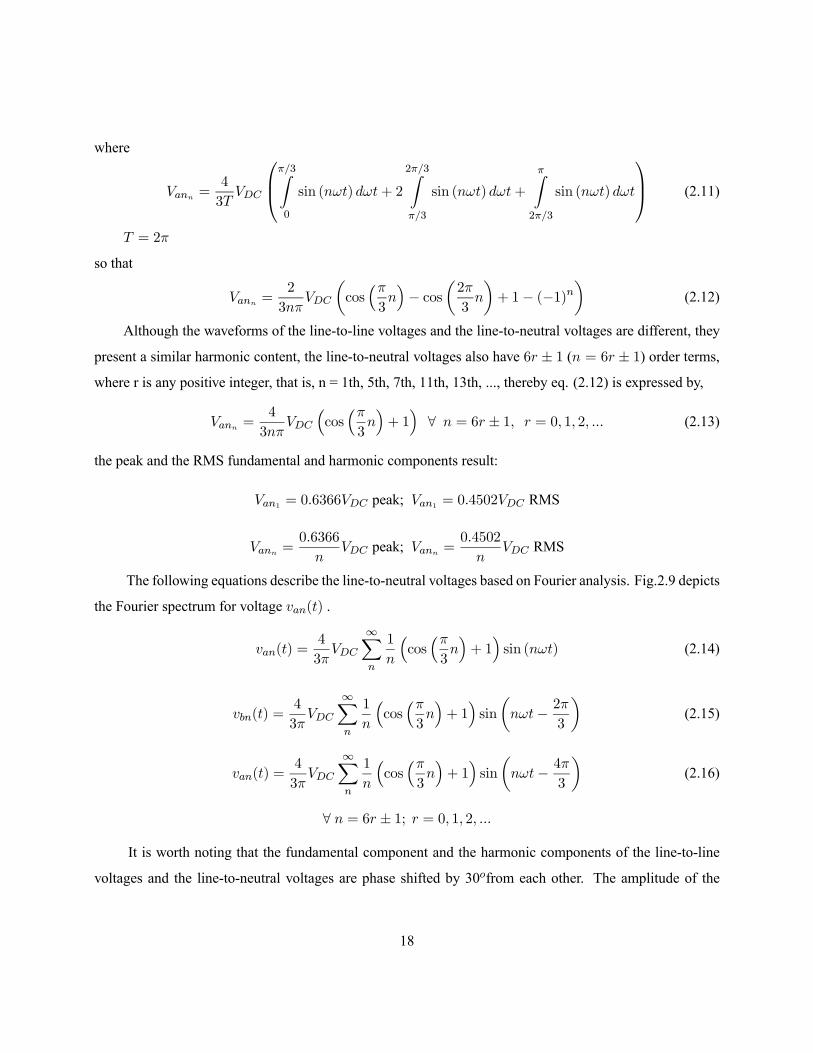
where
Vann =4
3TVDC
π/3Z0
sin (nωt) dωt+ 2
2π/3Zπ/3
sin (nωt) dωt+
πZ2π/3
sin (nωt) dωt
(2.11)
T = 2π
so that
Vann =2
3nπVDC
µcos³π3n´− cos
µ2π
3n
¶+ 1− (−1)n
¶(2.12)
Although the waveforms of the line-to-line voltages and the line-to-neutral voltages are different, they
present a similar harmonic content, the line-to-neutral voltages also have 6r ± 1 (n = 6r ± 1) order terms,
where r is any positive integer, that is, n = 1th, 5th, 7th, 11th, 13th, ..., thereby eq. (2.12) is expressed by,
Vann =4
3nπVDC
³cos³π3n´+ 1´∀ n = 6r ± 1, r = 0, 1, 2, ... (2.13)
the peak and the RMS fundamental and harmonic components result:
Van1 = 0.6366VDC peak; Van1 = 0.4502VDC RMS
Vann =0.6366
nVDC peak; Vann =
0.4502
nVDC RMS
The following equations describe the line-to-neutral voltages based on Fourier analysis. Fig.2.9 depicts
the Fourier spectrum for voltage van(t) .
van(t) =4
3πVDC
∞Xn
1
n
³cos³π3n´+ 1´sin (nωt) (2.14)
vbn(t) =4
3πVDC
∞Xn
1
n
³cos³π3n´+ 1´sin
µnωt− 2π
3
¶(2.15)
van(t) =4
3πVDC
∞Xn
1
n
³cos³π3n´+ 1´sin
µnωt− 4π
3
¶(2.16)
∀ n = 6r ± 1; r = 0, 1, 2, ...
It is worth noting that the fundamental component and the harmonic components of the line-to-line
voltages and the line-to-neutral voltages are phase shifted by 30ofrom each other. The amplitude of the
18

0 5 10 15 20 25 30 35 40 45 500
0.1
0.2
0.3
0.4
0.5
0.6
0.7
0.8
0.9
1
nth. harmonic
Mag
nitu
de (p
er u
nit f
unda
men
tal)
Fig. 2.9 vab(t) voltage Fourier spectrum
line-to-line voltages is√3 times the line-to-neutral voltage amplitude, and the harmonics components not
included in the set n = 12r ± 1 are in phase opposition. This is illustrated by the following expressions:
Vab1 =√3Van1
Vab5 = −√3Van5
Vab7 = −√3Van7
Vab11 =√3Van11
Vab13 =√3Van13
that may be reduced to the following one:
Vabn = (−1)r√3Vann (2.17)
where: n = 6r ± 1 and r = 0, 1, 2, ...
If the VSI of Fig.2.2 has a resistive load (unitary power factor) the diodes do not conduct at any
time, but if the load is inductive regardless of the power factor the conduction period of the transistors
would be between 90oand 180oand that of the diodes between 0oand 90o. The following figures illustrate
19

0 0 .0 1 0 .0 2 0 .0 3 0 .04 0 .0 5 0 .0 6 0 .0 7- 80
- 60
- 40
- 20
0
2 0
4 0
6 0
8 0
Am
p
0 0 .0 1 0 .0 2 0 .0 3 0 .04 0 .0 5 0 .0 6 0 .0 7- 10
0
1 0
2 0
3 0
4 0
5 0
6 0
7 0
Time ( s)
Am
p
iQ 1
i D 1
Ph as e a cu rre nt , i a(t)
T ra n si s tor Q 1 a n d d i od e D1 cu rren t; i Q1 ; iD 1
Fig. 2.10 0.5 inductive power factor load conduction period
the conduction period for the first transistor and diode. A wye connected load with a 0.5 inductive power
factor was considered in Fig.2.10 (R = 1 Ω , L = 4.5944 mH); in this case the transistors conduct during
120oand the diodes for 60o. In Fig.2.11 a wye connected load with a 0.8660 inductive power factor was
considered (R = 1 Ω, L = 1.5315 mH); in this case the transistors conduct during 150oand the diodes for 30o.
Finally, Fig.2.12 depicts a pure inductive load (zero power factor); it shows that for a pure reactive load the
conduction period for the transistors and diodes is equal, that is, 90o.
2.3 Static synchronous compensator (STATCOM) based on six-pulse VSI
The static compensators are devices with the ability to both generate and absorb reactive and active
power, but the most common applications are in reactive power exchange between the AC system and the
compensator.
The static synchronous compensator (STATCOM) based on six-pulse VSI, Fig.2.13, is the basic build-
ing block of high power static VAR compensator. In high power applications the six-pulse configuration
does not have an appropriate performance, because of it exhibits a high harmonic rate. Consequently, the
20

0 0 .0 1 0 .0 2 0 .0 3 0 .0 4 0 .0 5 0 .0 6 0 .0 7- 150
- 100
- 50
0
50
1 00
1 50
Am
p
0 0 .0 1 0 .0 2 0 .0 3 0 .0 4 0 .0 5 0 .0 6 0 .0 7- 20
0
20
40
60
80
1 00
1 20
Ti me ( s)
Am
p
iQ 1
iD 1
Ph ase a curre nt ; i a(t )
Transistor Q 1 and diode D 1 curr ent; iQ1 , iD1
Fig. 2.11 0.8660 inductive power factor load conduction period
0 0.01 0.02 0 .03 0.04 0.05 0.06-1
0
1
2
3
4
Tim e (s)
Am
p
i Q1i D1
0 0.01 0.02 0.03 0.04 0.05 0.06 0.07-4
-3
-2
-1
0
1
2
3
4
Am
p
Phase a current; ia(t )
Transistor Q1 and diode D1 current; iQ1, iD1
Fig. 2.12 Inductive load conduction period
21

Q1
Q4
Q3 Q5
Q6 Q2
D1 D3 D5
D1 D6 D2
a b c
g1 g3 g5
g4 g6 g2
L L L
C
ICD
vAN(t) vBN(t) vCN(t)
VCD
+
ia(t) ib(t) ic(t)
Fig. 2.13 Six-pulse VSI-STATCOM
current analysis is aimed to give us an important insight into the analysis of more complicated higher pulse
arrangements.
2.3.1 Reactive power exchange
The reactive power exchange between the AC system and the compensator is controlled by varying the
magnitude of the fundamental component of the inverter voltage above and below that of the AC system.
The compensator control is achieved by small variations in the switching angle of the semiconductor
devices, so that the fundamental component of the voltage produced by the inverter is forced to lag or
lead the AC system voltage by a few degrees. This causes active power to flow into or out of the inverter
22

modifying the value of the DC capacitor voltage, and consequently the magnitude of the inverter terminal
voltage and the resultant reactive power. If the compensator supplies only reactive power, the active power
provided by the DC capacitor is zero. Therefore, the capacitor does not change its voltage. One could say
then that the capacitor plays not any role in the reactive power generation [1].
2.3.1.1 Analysis of the AC current signals
The current flowing between the compensator and the AC system is determined by the voltage across
the tie inductor. Let the AC voltage be a pure sinusoidal function ean(t) = Vm sin (ωt), then the magnitude
of the fundamental and harmonic components are given by eqns. (2.18) and (2.19). From eq. (2.13)
van(t) = 0.6366VDC sin (ωt), then,
ia(t)1 = −Vm − 0.6366VDCωL
cos (ωt) ; (fundamental component)
ia(t)n =0.6366VDCn2ωL
cos (nωt) ; (nth harmonic component)
the fundamental current is also called fundamental reactive current Iq.
Ia1 = Iq =Vm − 0.6366VDC
ωL(2.18)
Ian = Iqn =0.6366VDCn2ωL
, n > 1 (2.19)
The fundamental current will be leading when Vm < 0.6366VDC ; that is, if the amplitude of the inverter
voltage is increased above that of the AC system (the current flows from the converter to the AC system); in
this case the compensator is seen as a capacitor by the AC system. The fundamental current will be lagging
when Vm > 0.6366VDC , that is, if the amplitude of the inverter voltage is decreased below that of the AC
system (the current flows from the AC system to the compensator); in this case the compensator is seen as a
inductor by the AC system, Fig.2.14.
From eq. (2.19) can be deduced that the harmonic currents only flow from the compensator to the
AC system. Fig.2.15 depicts the relationship between the DC voltage (VDC) and the fundamental reactive
current. The lower-order harmonic currents as a function of the fundamental reactive current are shown too.
Taking into account the voltage across the tie inductor over each 60oconduction interval, Fig.2.16, the
equation that describes the AC current ia(t), is derived. The other two-phase currents, ib(t) and ic(t), will
23

Lagging
Vm > 0.6366VDC
Leading
Vm < 0.6366VDC
VL
Ia1Ia1 Ian
Lagging
Vm > 0.6366VDC
Leading
Vm < 0.6366VDC
VL
Ia1Ia1 Ian
Fig. 2.14 Phase relationship between the inductor voltage VL and the fundamental curren Ia1
-1 .5 -1 - 0.5 0 0 .5 1 1 .50
0 .5
1
1 .5
2
Iq
DC
vol
tage
(p.u
)
-1 .5 -1 - 0.5 0 0 .5 1 1 .50
0 .0 2
0 .0 4
0 .0 6
0 .0 8
0 .1
0 .1 2
0 .1 4
Iq
I qn (n
th h
arm
onic
mag
nitu
de)
Iq 5Iq 7Iq 1 1
Leadi ng ( ca pa c iti ve re g io n) Lag g ing (i nduc t ive re g ion )
La g g ing (ind uc tiv e r eg i on ) Lea ding (ca p acit iv e r eg ion)
Fig. 2.15 Relationship between DC voltage, fundamental and harmonics current
24

0
0
ω t
3
π
3
2 π π
3
4 π
3
5 π π2
mV
mV−
D CV32
D CV
32
−
D CV31
D CV31
−
Fig. 2.16 AC system voltage and voltage compensator van(t)
be identical except phase shifted by 120oand 240o, respectively, from ia(t).
At any time vL(t) = Ld
dtia(t), where vL(t) is the instantaneous inductor voltage, which is the instan-
taneous difference across the AC system voltage, ean(t), and the compensator voltage van(t). The following
differential equations can be written for each 60oconduction interval.
• Interval: 0 ≤ ωt ≤ π/3
vL(t) = Vm sin (ωt)− 13VDC = L
d
dtia(t)
ia(t) = −VmωL
(cos (ωt)− 1)− 1
3LVDCt+ I0 (2.20)
where I0 is the initial condition at t = 0; ia(0) = I0.
• Interval: π/3 ≤ ωt ≤ 2π/3
vL(t) = Vm sin (ωt)− 23VDC = L
d
dtia(t)
ia(t) = −VmωL
(cos (ωt)− 0.5)−µ2
3Lt− 2π
9ωL
¶VDC + I1 (2.21)
where I1 = ia³ π
3ω
´• Interval: 2π/3 ≤ ωt ≤ π
25

vL(t) = Vm sin (ωt)− 13VDC = L
d
dtia(t)
ia(t) = −VmωL
(cos (ωt)− 0.5)−µ1
3Lt− 2π
9ωL
¶VDC + I2 (2.22)
where I2 = iaµ2π
3ω
¶It is known that in steady state the AC current waveform is symmetric, therefore,
ia
³ π
2ω
´= 0
taking into account the above property, the steady state initial condition I0 can be calculated as follows:
ia
³ π
2ω
´= −Vm
ωL
³cos³π2
´− 0.5
´−µ2
3L· π
2ω− 2π
9ωL
¶VDC + I1 = 0
I1 = −VmωL0.5 +
π
9ωLVDC (2.23)
I1 = ia
³ π
3ω
´= −Vm
ωL
³cos³π3
´− 1´− 1
3LVDC · π
3ω+ I0
I1 =VmωL0.5− π
9ωLVDC + I0 (2.24)
equating eqns. (2.23) and (2.24), the steady state condition is estimated:
I0 = −VmωL
+2π
9ωLVDC (2.25)
substituting eqn. (2.25) into eqn. (2.20) the steady state equations are derived,
ia(t) = −VmωL
cos (ωt)−µ1
3Lt− 2π
9ωL
¶VDC (2.26)
0 ≤ ωt ≤ π/3
ia(t) = −VmωL
cos (ωt)−µ2
3Lt− π
3ωL
¶VDC (2.27)
π/3 ≤ ωt ≤ 2π/3
ia(t) = −VmωL
cos (ωt)−µ1
3Lt− π
9ωL
¶VDC (2.28)
2π/3 ≤ ωt ≤ π
26

0 0 .0 1 0 .0 2 0 .03 0 .0 4 0 .0 5 0 .0 6- 2
- 1
0
1
2 Ph ase a : i a (t )
Am
p
0 0 .0 1 0 .0 2 0 .03 0 .0 4 0 .0 5 0 .0 6- 2
- 1
0
1
2 Ph ase b: ib( t )
Am
p
0 0 .0 1 0 .0 2 0 .03 0 .0 4 0 .0 5 0 .0 6- 2
- 1
0
1
2 Ph ase c : ic( t )
T i me ( s)
Am
p
L ea di ng Lag g ing
Fig. 2.17 AC current waveform
Over the interval π ≤ ωt < 2π the AC current waveform is the negative respect to that described in the
above equations. Fig.2.17 depicts the AC current waveform. For the leading case VDC = 6 V, Vm = 2.5 V,
and L = 3 mH were used; and VDC = 6 V, Vm = 4.5 V, and L = 3 mH for the lagging case.
2.3.1.2 Conduction period transistors and diodes
With the precedent AC current equations it is possible to predict the conduction period of each transistor
and diode. When only reactive power is generated (zero power factor) the transistors and diodes of the
inverter circuit conduct for 90o.
If the compensator is absorbing reactive power, the transistors naturally turn off at zero current. When
it is generating reactive power, the transistors turn off at the peak of the AC current waveform. The following
algorithm proposes a way to determining the conduction period of each device at any power factor based on
the AC current waveforms and the firing control signals.
• Leg 1Pulse g1 on:
– If ia(t) is positive,D1 conducts.
27

– If ia(t) is negative, Q1 conducts.
Pulse g4 on:
– If ia(t) is positive, Q4 conducts.
– If ia(t) is negative,D4 conducts.
• Leg 2Pulse g3 on:
– If ib(t) is positive,D3 conducts.
– If ib(t) is negative, Q3 conducts.
Pulse g6 on:
– If ib(t) is positive, Q6 conducts.
– If ib(t) is negative, D6 conducts.
• Leg 3Pulse g5 on:
– If ic(t) is positive, D5 conducts.
– If ic(t) is negative, Q5 conducts.
Pulse g2 on:
– If ic(t) is positive, Q2 conducts.
– If ic(t) is negative,D2 conducts.
The Q1 andD1 conduction period for leading and lagging current are presented in Fig.2.18.
2.3.1.3 Capacitor current
The capacitor current is made up of segments of the three AC phase currents and is dependent on which
semiconductor devices are conducting over each 60ointerval. The capacitor current can be deduced in the
following way:
iD1(t) + iD3
(t) + iD5(t) + iDC(t) = iQ1
(t) + iQ3(t) + iQ5
(t)
so that
iDC(t) = iQ1(t) + iQ3
(t) + iQ5(t)− (iD1
(t) + iD3(t) + iD5
(t)) (2.29)
28

0 0 .0 1 0 .0 2 0 .03 0 .04 0 .0 5 0 .0 60
0 .5
1
1 .5Q 1 cu rre nt : iQ1 ( t)
Am
p
L ea dingLagg ing
0 0 .0 1 0 .0 2 0 .03 0 .04 0 .0 5 0 .0 60
0 .5
1
1 .5
T ime ( s)
Am
p
D 1 c urre nt : iD 1 (t )
Fig. 2.18 Q1 andD1 conduction period
• Interval: 0 ≤ ωt ≤ π/3
iDC(t) = ia(t) + ic(t)
where
ic(t) = −VmωL
cos
µωt+
2π
3
¶−µ1
3Lt+
π
9ωL
¶VDC
so that
iDC(t) =VmωL
sin³ωt− π
6
´−µ2
3Lt− π
9ωL
¶VDC (2.30)
• Interval: π/3 ≤ ωt ≤ 2π/3iDC(t) = ia(t)
iDC(t) =VmωL
sin³ωt− π
2
´−µ2
3Lt− π
3ωL
¶VDC (2.31)
• Interval: 2π/3 ≤ ωt ≤ π
iDC(t) = ia(t) + ib(t)
where
ib(t) = −VmωL
cos
µωt− 2π
3
¶−µ1
3Lt− 4π
9ωL
¶VDC
29

so that
iDC(t) =VmωL
sin
µωt− 5π
6
¶−µ2
3Lt− 5π
9ωL
¶VDC (2.32)
These expressions are equivalent except phase shifted by 60oamong them; therefore the capacitor cur-
rent waveform over each of the remaining three conduction periods is identical to that described by eq.
(2.30) and yields, in a repetitive waveform, six times the corresponding AC power system frequency.
2.3.1.4 DC capacitor voltage
The previous analysis assumes a constant DC voltage; it is equivalent to consider an infinite capacitor
and consequently zero DC ripple voltage. If a finite capacitor is considerated a DC ripple voltage exist which
is dependent on the capacitor value and the capacitor current.
Assuming that the capacitor current remains significantly unchanged from that given by eqn. (2.30),
the capacitor voltage can be estimated; under this condition a minimum DC ripple voltage is obtained [ 4].
The capacitor voltage over the first 60operiod is given by:
vcap(t) =1
C
tZ0
iDC(t)dt+ V0 (2.33)
where V0 is the initial condition at t = 0; V0 = vcap(0). Substituting eqn. (2.30) into eqn. (2.33)
vcap(t) = − Vmω2LC
cos³ωt− π
6
´− 1
3LCVDCt
2 +π
9ωLCVDCt+
√3Vm
2ω2LC+ V0 (2.34)
The value of V0 is calculated from the average component of eq. (2.34) with a period T = π/3ω . At
the same time the DC voltage level VDC is determined.
VDC =1
T
π/3ωZ0
vcap(t)dt (2.35)
VDC =3ω
π
Ã− Vmω3LC
− π3
243ω3LCVDC +
π3
162ω3LC+
√3π
6ω3LCVm +
π
3ωV0
!Simplifying this expression results:
V0 = 0.0889Vm
ω2LC− 0.0609 1
ω2LCVDC + VDC (2.36)
30

0
-1
-0.5
0
0.5
1
(a)
Am
p (p
u)
0
-1
-0.5
0
0.5
1
(b)
Am
p (p
u)
ωt
ωt
0
-1
-0.5
0
0.5
1
(a)
Am
p (p
u)
0
-1
-0.5
0
0.5
1
(b)
Am
p (p
u)
ωt
ωt
Fig. 2.19 Capacitor current; a)generating reactive power; b)absorbing reactive power
The current and voltage waveforms of the capacitor obtained using the expressions (2.30) and (2.34)
are shown in Fig.2.19 and Fig.2.20. Fig.2.20 illustrates that the peak capacitor voltage Vpk, occurs when the
compensator is generating reactive power (leading current), ωt = 30o.
Vpk = vcap
³ π
6ω
´= − Vm
ω2LC− 1
3LCVDC
³ π
6ω
´2+
π
9ωLCVDC
³ π
6ω
´+
√3
2ω2LCVm
+0.0889Vm
ω2LC− 0.0609 1
ω2LCVDC + VDC
Simplifying, gives rises to:
Vpk = −0.0451 Vmω2LC
+ 0.03051
ω2LCVDC + VDC (2.37)
The above peak voltage is important because of the capacitor voltage is applied directly to the semi-
conductor devices, therefore those ones must be able to support that voltage.
Fig.2.21 shows the line-to-neutral voltage, van(t), and the line-to-line voltage, vab(t), when the com-
pensator is operated with a finite capacitor as a DC source. This figure illustrates the capacitor ripple voltage
effect. The capacitor voltage and current waveforms are presented in Fig.2.22. These results were obtained
using the PSCAD\EMTDC software with the following parameters: C = 500 µF, L = 3 mH, Vm = 2.5 V,
31
00.85
0.9
0.95
1
1.05
1.1
(a)
Vol
ts (
pu)
00.98
0.99
1
1.01
1.02
1.03
1.04
(b)
Vol
ts (
pu)
ωt
ωt
00.85
0.9
0.95
1
1.05
1.1
(a)
Vol
ts (
pu)
00.98
0.99
1
1.01
1.02
1.03
1.04
(b)
Vol
ts (
pu)
ωt
ωt
Fig. 2.20 DC capacitor voltage; a)generating reactive power; b)absorbing reactive power
and VDC = 6 V.
If the compensator only exchange reactive power the voltage capacitor does not vary, thus the capacitor
current is the one shown in Fig.2.19. Based on Fourier analysis it is given by:
iDC(t) =∞Xn=1
IDCn sin (nωt) (2.38)
where:
IDCn =2
T
TR0
iDC(t) sin (nωt) dt
T =π
3ωThereby the capacitor voltage is made up only by sinusoidal functions with fixed amplitude and a DC
offset, Fig.2.20.
2.3.2 Reactive and active power exchange
Considering a phase shift φ across the AC power system and the fundamental compensator voltage,
Fig.2.23, both reactive and active power is exchanged. To obtain the AC current equations a similar proce-
32

0 0 .00 5 0 .0 1 0 .0 1 5 0 .0 2 0 .0 25 0 .03 0 .035 0 .0 4 0 .0 4 5 0 .0 5- 5
0
5
Vol
ts
0 0 .00 5 0 .0 1 0 .0 1 5 0 .0 2 0 .0 25 0 .03 0 .035 0 .0 4 0 .0 4 5 0 .0 5- 8
- 6
- 4
- 2
0
2
4
6
8
Ti me ( s)
Vol
ts
P h a se to n eu tra l v o l tag e; v an(t )
Ph as e to p h a se v o l tag e; v ab(t )
Fig. 2.21 Voltage waveforms with a finite DC capacitor
0 0.005 0.01 0.015 0.02 0.025 0.03 0.035 0.04 0.045 0.05-0.8
-0.6
-0.4
-0.2
0
0.2
0.4
0.6
0.8
Am
p
c ur rent wavefor m
0 0.005 0.01 0.015 0.02 0.025 0.03 0.035 0.04 0.045 0.050
1
2
3
4
5
6
7
Time (s)
Vol
ts
DC c apac itor voltage
Fig. 2.22 Capacitor current and DC capacitor voltage waveform
33

0
0
D Cv32
mv
D Cv31
D Cv31−
DCv32−
mv−
3π
32π π
34 π
35 π π2
tω
Fig. 2.23 AC system voltage and compensator voltage; van(t)
dure to that presented in the section 2.3.1.1 is carried out.
• Interval: 0 ≤ ωt ≤ π/3
vL(t) = Vm sin (ωt− φ)− 13VDC = L
d
dtia(t)
ia(t) = −VmωL
(cos (ωt− φ)− cos (φ))− 1
3LVDCt+ I0 (2.39)
where I0 is the initial condition at t = 0; ia(0) = I0.
• Interval: π/3 ≤ ωt ≤ 2π/3
vL(t) = Vm sin (ωt− φ)− 23VDC = L
d
dtia(t)
ia(t) = −VmωL
³cos (ωt− φ)− cos
³π3− φ
´´−µ2
3Lt− 2π
9ωL
¶VDC + I1 (2.40)
where: I1 = ia³ π
3ω
´• Interval: 2π/3 ≤ ωt ≤ π
vL(t) = Vm sin (ωt− φ)− 13VDC = L
d
dtia(t)
ia(t) = −VmωL
µcos (ωt− φ)− cos
µ2π
3− φ
¶¶−µ1
3Lt− 2π
9ωL
¶VDC + I2 (2.41)
34

where: I2 = iaµ2π
3ω
¶Taking into account that ia(0) = −ia
³πω
´, the steady state initial condition I0 can be calculated,
I0 = −ia³πω
´=VmωL
µcos (π − φ)− cos
µ2π
3− φ
¶¶+
µ1
3L· πω− 2π
9ωL
¶VDC − I2
so that
I0 =VmωL
µcos (π − φ)− cos
µ2π
3− φ
¶¶+
π
9ωLVDC − I2 (2.42)
where:
I2 = −VmωL
µcos
µ2π
3− φ
¶− cos
³π3− φ
´¶− 2π
9ωLVDC + I1 (2.43)
I1 = ia
³ π
3ω
´= −Vm
ωL
³cos³π3− φ
´− cos (φ)
´− π
9ωLVDC + I0 (2.44)
Substituting eqns. (2.43) and (2.44) into eqn. (2.42) yields
I0 = −VmωL
cos (φ) +2π
9ωLVDC (2.45)
using eqn. (2.45) the steady state equations are:
ia(t) = −VmωL
cos (ωt− φ)−µ1
3Lt− 2π
9ωL
¶VDC (2.46)
0 ≤ ωt ≤ π/3
ia(t) = −VmωL
cos (ωt− φ)−µ2
3Lt− π
ωL
¶VDC (2.47)
π/3 ≤ ωt ≤ 2π/3
ia(t) = −VmωL
cos (ωt− φ)−µ1
3Lt− π
9ωL
¶VDC (2.48)
2π/3 ≤ ωt ≤ π
Over the interval π ≤ ωt < 2π the AC current waveform is the negative of that described in the above
equations. As the phase shift φ increases the AC current changes regarding to the one shown in Fig.2.17.
Fig.2.24 illustrates the AC current with φ = 15o.
35

0 0.005 0.01 0.015 0.02 0.0 25 0.03 0 .035 0.04 0 .045 0.05-2
-1
0
1
2
Am
p
0 0.005 0.01 0.015 0.02 0.0 25 0.03 0 .035 0.04 0 .045 0.05-2
-1
0
1
2
Am
p
0 0.005 0.01 0.015 0.02 0.0 25 0.03 0 .035 0.04 0 .045 0.05-2
-1
0
1
2
Tim e (s)
Am
p
Phase a: ia(t)
Phase b: ib(t)
Phase c: ic(t)
Fig. 2.24 AC current waveform with φ = 15o
2.3.2.1 Capacitor current
The capacitor current is obtained in a similar manner to that presented previously and has a similar
behaviour, a waveform made up by six segments where each segment can be represented by eq. (2.49) with
a phase shifted by 60ofrom each other.
iDC(t) =VmωL
sin³ωt− φ− π
6
´−µ2
3Lt− π
9ωL
¶VDC (2.49)
0 ≤ ωt ≤ π/3
It is noteworthy that if the angle φ increases the capacitor current would have a greater DC level, this
effect is illustrated in Fig.2.25 where iDC(t) is presented taking into account φ = 2o and φ = 15o.
If an angle φ exists between the AC power system voltage and the fundamental compensator voltage
the instantaneous capacitor voltage and current, based on Fourier analysis are given by:
iDC(t) = IDC0 +∞Pn=1
IDCn sin (nωt)
vcap(t) = VDC0 +∞Pn=1
VDCn cos (nωt)
36
0 0.002 0.004 0.006 0.008 0.01 0 .012 0 .014 0.0 16 0.018-0. 5
0
0.5
1
1.5
T ime (s)
Am
p
Instantan e ou s DC c urren t w ith φ = 15º
0 0.002 0.004 0.006 0.008 0.01 0 .012 0 .014 0.0 16 0.018-1
-0. 5
0
0.5
1
Am
p
Instantan eou s D C cur ren t w ith φ = 2º
Fig. 2.25 Instantaneous capacitor current
The above expressions show that a DC power or active power flows through the DC side, thus the
capacitor voltage will be increased or decreased, depending if the IDC0 is positive or negative. To reveal this
effect consider the circuit shown in Fig.2.26.
The circuit is initially at steady state with φ = 0o, at time t = 0.0333 s the angle φ was stepped from
0oto -0.5o. Fig.2.27 shows the capacitor voltage. This figure illustrates that the phase shift φ affect the
capacitor voltage, due to the DC component into iDC(t), that is, the active power exchange, and that the
mechanism of phase angle adjustment is used to control the VAR generation or absorption by increasing or
decreasing the capacitor voltage, and thereby the amplitude of the output voltage produced by the converter.
The steady state DC component of the capacitor current is given by:
IDC0 =1
T
TZ0
iDC(t)dt
where iDC(t) is given by eq. (2.49) and T = π/3ω, so that
IDC0 = −3VmπωL
sin (φ) (2.50)
37

IC(t) 500µF
Fig. 2.26 Test circuit
If the converter only supplies reactive power the AC power system voltage and the fundamental con-
verter voltage are in phase, if the converter is ideal (without losses). In practical converters, however the
semiconductor switches are not lossless, and therefore the energy stored in the DC capacitor would be used
up by the internal losses. However, these losses can be supplied from the AC system by making the output
voltages of the converter lag the AC system voltages by a small angle; this allows an active power flow from
the AC system to the converter, which compensates the converter losses and keeps the capacitor voltage at
the desired level.
The above concept is illustrated in Fig.2.28. The system is operating in steady state with a fixed DC
source at t = 0.1 s, the DC source is changed by a DC capacitor. In Fig.2.28(a) both the AC system voltage
and the compensator voltage are in phase, in this case the energy stored in the DC capacitor is used up by
the internal losses. In Fig.2.28(b) with a small angle between the AC system voltage and the compensator
voltage the losses are supplied from the AC system and the capacitor voltage is kept at the desired level.
Fig.2.28 was obtained using PSCAD/EMTDC.
2.4 12-pulse converter
The six-pulse STATCOM is the simplest arrangement used in this kind of devices; in high power ap-
plications it does not offer a good performance, due to the high harmonic content. Combining two six-pulse
converters, a better performance is obtained. This new configuration is called twelve-pulse STATCOM. The
twelve-pulse circuit is the lowest practical pulse-numbered circuit for power system application to achieve
a satisfactory harmonic behaviour [4].
38

0 0.02 0.04 0.06 0.08 0.1 0.125
5.5
6
6.5
7
7.5
8
8.5
9
9.5
Time (s)
Vol
ts
Fig. 2.27 Instantaneous capacitor voltage
0 0.05 0.1 0.15 0.2 0.25 0.3-1.5
-1
-0.5
0
0.5
1
1.5
(a)
Am
p.
0 0.05 0.1 0.15 0.2 0.25 0.3-1.5
-1
-0.5
0
0.5
1
1.5
(b)Time (s)
Am
p.
Fig. 2.28 AC instantaneous current with: a)φ = 0o;b)φ = −0.5o
39

The six-pulse converter output are the line-to-line voltages, vab(t), vbc(t), and vca(t). vab(t) is given by
eq. (2.1), expressing it by its Fourier series results:
vab(t) = Vab1 sin (ωt+ 30o) + Vab5 sin (5ωt+ 150
o) + Vab7 sin (7ωt+ 210o)
+Vab11 sin (11ωt+ 330o) + Vab13 sin (13ωt+ 30
o) + Vab17 sin (17ωt+ 150o)
+Vab19 sin (19ωt+ 210o) + Vab23 sin (23ωt+ 330
o) + ... (2.51)
If this compensator is connected to a Y −Y transformer with a 1:1 turn ratio, the line-to-neutral voltage,
van(t) is given by,
van(t) =1√3(Vab1 sin (ωt)− Vab5 sin (5ωt)− Vab7 sin (7ωt) + Vab11 sin (11ωt)
+Vab13 sin (13ωt)− Vab17 sin (17ωt)− Vab19 sin (19ωt) + Vab23 sin (23ωt) + ...) (2.52)
van(t) =1
3
∞Xn=1
Vabn(−1)r sin (nωt) (2.53)
∀ n = 6r ± 1, r = 0, 1, 2, ...
From eqns. (2.51) and (2.52) could be noted that the line-to-line voltage amplitudes are√3 times
the line-to-neutral voltage amplitudes and the harmonic components not included in the set n = 12r ± 1,where r = 0, 1, 2, ..., are in phase opposition. This feature is useful to cancel the harmonic components not
included in the set n = 12r ± 1.Suppose that a second six-pulse converter produces line-to-line voltages lagged 30owith respect to the
other converter and with the same magnitude. That is,
vab(t)2 = Vab1 sin (ωt) + Vab5 sin (5ωt) + Vab7 sin (7ωt) + Vab11 sin (11ωt)
+Vab13 sin (13ωt) + Vab17 sin (17ωt) + Vab19 sin (19ωt) + Vab23 sin (23ωt) + ... (2.54)
vab(t)2 =∞Xn=1
Vabn sin (nωt) (2.55)
If the second converter is connected to a ∆ − Y transformer with a 1 : 1/√3 turn ratio, the line-to-
neutral voltage in the Y -connected secondary would be:
vanY (t)2 =1√3(Vab1 sin (ωt) + Vab5 sin (5ωt) + Vab7 sin (7ωt) + Vab11 sin (11ωt)
40

+Vab13 sin (13ωt) + Vab17 sin (17ωt) + Vab19 sin (19ωt) + Vab23 sin (23ωt) + ...)(2.56)
vanY (t)2 =1√3
∞Xn=1
Vabn sin (nωt) (2.57)
∀ n = 6r ± 1, r = 0, 1, 2, ...
then the line-to-line voltage in the wye-side is,
vabY (t)2 = Vab1 sin (ωt+ 30o)− Vab5 sin (5ωt+ 150o)− Vab7 sin (7ωt+ 210o)
+Vab11 sin (11ωt+ 330o) + Vab13 sin (13ωt+ 30
o)− Vab17 sin (17ωt+ 150o)−Vab19 sin (19ωt+ 210o) + Vab23 sin (23ωt+ 330o) + ... (2.58)
vabY (t)2 =∞Xn=1
Vabn(−1)r sin
³nωt+
π
6n´
(2.59)
∀ n = 6r ± 1, r = 0, 1, 2, ...
that can be expressed in other form,
vabY (t)2 =√3∞Xn=1
Vann sin³nωt+
π
6n´
(2.60)
∀ n = 6r ± 1, r = 0, 1, 2, ...
The two waveforms given by eqns. (2.1) and (2.59) are added using a summing transformer to give a
third waveform vab(t)12 closer to being a sine wave; this voltage is named twelve-pulse voltage,
vab(t)12 = vab(t) + vabY (t)2 (2.61)
vab(t)12 = 2(Vab1 sin (ωt+ 30o) + Vab11 sin (11ωt+ 330
o) + Vab13 sin (13ωt+ 30o)
+Vab23 sin (23ωt+ 330o) + ...) (2.62)
thus, vab(t)12 is the line-to-line voltage of a twelve-pulse converter. These waveforms are shown in Fig.2.29.
In the arrangement of Fig.2.30, the two six-pulse converters are connected in parallel on the same DC bus,
working together as a twelve-pulse VSI-STATCOM.
41
(a)
(b)Time (s)
DCV5774.0
DCV1547.1DCV
DCV5774.0−
DCV1547.1−DCV−
6π
2π
32π π π2 π3 π4 π5
tω
6π
2π
32π π π2 π3 π4 π5
tω
0
DCV5774.0
DCV5774.0−
DCV5774.1
DCV5774.1−
DCV1547.2
DCV1547.2−
0
)t(vab
2abY )t(v
(a)
(b)Time (s)
DCV5774.0
DCV1547.1DCV
DCV5774.0−
DCV1547.1−DCV−
6π
2π
32π π π2 π3 π4 π5
tω
6π
2π
32π π π2 π3 π4 π5
tω
0
DCV5774.0
DCV5774.0−
DCV5774.1
DCV5774.1−
DCV1547.2
DCV1547.2−
0
)t(vab
2abY )t(v
Fig. 2.29 a)vab(t) and vabY (t)2; b)12-pulse voltage
six-pulse converter
six-pulse converter
vAN(t) v BN(t) vCN(t )
ia(t )
ib(t)
ic(t )
iC D12(t)
C VDC
+
Y-Y
Y- ∆
ia 1(t)
ia2(t)
Fig. 2.30 12-pulse VSI-STATCOM
42

Van(t)
Vbn(t)
Vcn(t)
DCV31
DCV31
DCV31
DCV31
−
DCV31
−
DCV31
−
DCV9107.0
DCV9107.0
DCV9107.0
DCV9107.0−
DCV9107.0−
DCV9107.0−
DCV2440.1
DCV2440.1
DCV2440.1
DCV2440.1−
DCV2440.1−
DCV2440.1−
0
0
0
2π π π2 π3 π4 π5
tω
Van(t)
Vbn(t)
Vcn(t)
DCV31
DCV31
DCV31
DCV31
−
DCV31
−
DCV31
−
DCV9107.0
DCV9107.0
DCV9107.0
DCV9107.0−
DCV9107.0−
DCV9107.0−
DCV2440.1
DCV2440.1
DCV2440.1
DCV2440.1−
DCV2440.1−
DCV2440.1−
0
0
0
2π π π2 π3 π4 π5
tω
Fig. 2.31 12-pulse STATCOM line-to-neutral voltages
The twelve-pulse voltage given by eq. (2.61) expressed as a Fourier series is given by:
vab(t)12 =∞Xn=1
Vab12n sin³nωt+
π
6n´
(2.63)
∀ n = 12r ± 1, r = 0, 1, 2, ...
where:
Vab12n = Vabn +√3Vann
Vab12n =√34
nπVDC , ∀ n = 12r ± 1, r = 0, 1, 2, ... (2.64)
The line-to-neutral voltages are shown in Fig.2.31.
From Fig.2.32 can be observed that the twelve-pulse voltage vab(t)12, holds only harmonics of order
n = 12r ± 1, where r is any positive integer, that is, n = 1th, 11th, 13th, 23th, 25th..., with amplitudes
1/11th, 1/13th, 1/23th, 1/25th..., respectively.
43

2.4.1 AC current signals
Applying a similar procedure to that presented in the previous section, the AC current analysis is
carried out. Let the AC voltage be a pure sinusoidal function, ean(t) = Vm sin (ωt) , then the magnitude
of the fundamental and harmonics components are given by eq. (2.65) and eq. (2.66), where van1(t) =
1.2732VDC sin (ωt).
ia(t)1 = −Vm − 1.2732VDCωL
cos (ωt) ; (fundamental component)
ia(t)n =1.2732VDCn2ωL
cos (nωt) , ∀ n > 1; (nth harmonic component)
so that,
Ia1 = Iq =Vm − 1.2732VDC
ωL(2.65)
Ian = Iqn =1.2732VDCn2ωL
, ∀ n > 1 (2.66)
From now on, voltages vab(t), vbc(t) and vca(t) will be referred as the twelve-pulse STATCOM line-
to-line voltages and the voltages van(t), vbn(t) and vcn(t) as the twelve-pulse STATCOM line-to-neutral
voltages.
The fundamental current will be leading when Vm < 1.2732VDC ; thus, the compensator is seen as a
capacitor by the AC system and the current flows from the compensator to the AC system; the fundamental
current will be lagging when Vm > 1.2732VDC , thus the compensator behaves as an inductor by the AC
system and the current flows from the AC system to the compensator. Fig.2.33 exhibits the phasorial diagram
across the tie inductor and the AC current.
Fig.2.34 depicts the relationship between the DC voltage (VDC) and the fundamental reactive current.
The lower-order harmonic currents as a function of the fundamental reactive current are displayed too.
To obtain the AC current equations, the procedure is carried out in a similar way as that of the six-pulse
circuit, taking into account that the width over each conduction period is 30o, Fig.2.35.
• Interval 0 ≤ ωt < π/6
44

0 5 10 15 20 25 30 35 40 45 500
0.1
0.2
0.3
0.4
0.5
0.6
0.7
0.8
0.9
1
nth. harmonic
Mag
nitu
de(p
er u
nitf
unda
men
tal)
Fig. 2.32 vab(t)12 voltage Fourier spectrum
Ia1IanIa1
VL
Lagging
Vm > 1.2732VDC
Leading
Vm < 1.2732VDC
Ia1IanIa1
VL
Lagging
Vm > 1.2732VDC
Leading
Vm < 1.2732VDC
Fig. 2.33 Phasorial diagram
45

-2 -1.5 -1 -0.5 0 0. 5 1 1. 5 20
0.5
1
1.5
2
Lagging (inductive region) Iq Leading (capacitive region)
DC v
olta
ge (p
.u)
-2 -1.5 -1 -0.5 0 0. 5 1 1. 5 20
0.005
0.01
0.015
0.02
0.025
0.03
0.035
Lagging (inductive region) Iq Leading (capacitive region)
I qn (n
th h
arm
onic
mag
nitu
de) I q11
I q13 I q23
Fig. 2.34 Relationship between the DC voltage and the fundamental and harmonics current
mV
DCV31
DCV31−
DCV9107.0
DCV9107.0−
DCV2440.1
DCV2440.1−
mV−
6π
3π
2π
32π
65π π
67π
34π
23π
35π
611π π2
tω
Fig. 2.35 AC system voltage and fundamental voltage compensator van(t)
46

vL(t) = Vm sin (ωt)− 13VDC = L
d
dtia(t)
ia(t) = −VmωL
(cos (ωt)− 1)− 1
3LVDCt+ I0 (2.67)
where I0 is the initial condition at t = 0; ia(0) = I0.
• Interval π/6 ≤ ωt < π/3
vL(t) = Vm sin (ωt)− 0.9107VDC = L ddtia(t)
ia(t) = −VmωL
Ãcos (ωt)−
√3
2
!−µ0.9107
Lt− 0.9107π
6ωL
¶VDC + I1 (2.68)
where: I1 = ia³ π
6ω
´• Interval π/3 ≤ ωt < π/2
vL(t) = Vm sin (ωt)− 1.2440VDC = L ddtia(t)
ia(t) = −VmωL
(cos (ωt)− 0.5)−µ1.2440
Lt− 1.2440π
3ωL
¶VDC + I2 (2.69)
where: I2 = ia³ π
3ω
´In steady state ia
³ π
2ω
´= 0, then the steady state initial condition I0 is computed as:
ia
³ π
2ω
´= −Vm
ωL(−0.5)−
µ1.2440
L· π
2ω− 1.2440π
3ωL
¶VDC + I2 = 0
I2 = − Vm2ωL
+1.2440π
6ωLVDC (2.70)
I2 = ia
³ π
3ω
´= −Vm
ωL
Ã1
2−√3
2
!−µ0.9107
L· π
3ω− 0.9107π
6ωL
¶VDC + I1
I1 = −√3Vm2ωL
+2.1547π
6ωLVDC (2.71)
I1 = ia
³ π
6ω
´= −Vm
ωL
Ã√3
2− 1!− 1
3L· π
6ωVDC + I0
I0 = −VmωL
+7.4641π
18ωLVDC (2.72)
47

Substituting eq. (2.72) into eqn. (2.67) the ia(t) steady state equations are,
ia(t) = −VmωL
cos (ωt)−µ1
3Lt− 7.4641π
18ωL
¶VDC (2.73)
0 ≤ ωt < π/6
ia(t) = −VmωL
cos (ωt)−µ0.9107
Lt− 3.0654π
6ωL
¶VDC (2.74)
π/6 ≤ ωt < π/3
ia(t) = −VmωL
cos (ωt)−µ1.2440
Lt− 3.7320π
6ωL
¶VDC (2.75)
π/3 ≤ ωt < 2π/3
ia(t) = −VmωL
cos (ωt)−µ0.9107
Lt− 2.3988π
6ωL
¶VDC (2.76)
2π/3 ≤ ωt < 5π/6
ia(t) = −VmωL
cos (ωt)−µ1
3Lt+
1.4641π
18ωL
¶VDC (2.77)
5π/6 ≤ ωt < π
Over the interval π ≤ ωt < 2π the AC current waveform is the negative of that described for the above
expressions. Fig.2.36 shows the ia(t) AC current waveform. For the leading case VDC = 3.0 V; Vm = 2.5
V and L = 3 mH were used; VDC = 3.0 V; Vm = 4.5 V and L = 3 mH for the lagging case.
2.4.1.1 Six-pulse AC current
The current flowing into the wye-connected secondary of both transformers (Y − Y and ∆ − Y ) is
equal to the AC line current, this is due to both secondary windings are connected in series. Using the
instantaneous power P (t) the AC current of each six-pulse VSI can be obtained.
Y − Y connection
• Interval 0 ≤ ωt < π/6
Pa(t)s = van(t)sia(t) (2.78)
where: Pa(t)s is the phase ”a” instantaneous power in the secondary winding.
48

van(t)s =1
3VDC is the line-to-neutral voltage in the secondary winding.
so that,
Pa(t)s =1
3VDC
µ−VmωL
cos (ωt)−µ1
3Lt− 7.4641π
18ωL
¶VDC
¶(2.79)
At the primary side the instantaneous power is:
Pa(t)p = van(t)pia1(t) (2.80)
where: Pa(t)p is the phase ”a” instantaneous power in the primary winding.
van(t)p =1
3VDC is the line-to-neutral voltage in the primary winding.
ia1(t) is the AC current in the primary windingthen,
Pa(t)p =1
3VDCia1(t) (2.81)
Neglecting losses, the instantaneous power in both windings is equal, then the AC current in the primary
winding is:
ia1(t) = −VmωL
cos (ωt)−µ1
3Lt− 7.4641π
18ωL
¶VDC (2.82)
therefore the wye-connected primary current is equal to the AC line current.
∆− Y connection
The instantaneous phase ’a’ power of the∆− Y transformer is given by:
Pa(t)s = van(t)sia(t) = Pab(t) = vab(t)piba(t) (2.83)
where: vab(t)p is the line-to-line voltage in the primary winding (∆).
iba(t) is the current in the primary winding.
van(t)s is the line-to-neutral voltage in the secondary winding (Y ).
Due to
vab(t)p =√3van(t)s (2.84)
then
iba(t) =1√3ia(t) (2.85)
49

0 0.005 0 .01 0.015 0 .02 0.025 0 .03 0.035 0.04 0 .045 0 .05-1 .5
-1
-0 .5
0
0 .5
1
1 .5
Time (s )
Am
p
LeadingLagging
0 0.005 0 .01 0.015 0 .02 0.025 0 .03 0.035 0.04 0 .045 0 .05-1 .5
-1
-0 .5
0
0 .5
1
1 .5
Time (s )
Am
p
LeadingLagging
Fig. 2.36 AC current waveform, ia(t)
icb(t) =1√3ib(t) (2.86)
iac(t) =1√3ic(t) (2.87)
The AC current of the second VSI ia(t)p is given by:
ia2(t) = iba(t)− iac(t) (2.88)
over the interval 0 ≤ ωt < π/6 the phase current of the second six-pulse VSI is given by eq. (2.89).
ia2(t) = −VmωL
cos³ωt− π
6
´+
µ1
3Lt+
6.4641π
18ωL
¶VDC (2.89)
From the above analysis can be concluded that the current flowing into the delta-connected primary is
phase-shifted by 30owith respect to the wye-connected primary. Fig.2.37 depicts the AC current waveform
of each six-pulse VSI and the current across the diode and transistor one, D1, Q1 of the first six-pulse VSI
is shown in Fig.2.38.
50

0 0.005 0.01 0.015 0.02 0.025 0.03 0.035 0.04 0.045 0.05-2
-1
0
1
2Phase a: ia(t)
Am
p
0 0.005 0.01 0.015 0.02 0.025 0.03 0.035 0.04 0.045 0.05-2
-1
0
1
2Phase b: i
b(t)
Am
p
0 0.005 0.01 0.015 0.02 0.025 0.03 0.035 0.04 0.045 0.05-2
-1
0
1
2Phase c: ic(t)
Time (s)Y-Y VSI ∆-Y VSI
Am
p
0 0.005 0.01 0.015 0.02 0.025 0.03 0.035 0.04 0.045 0.05-2
-1
0
1
2Phase a: ia(t)
Am
p
0 0.005 0.01 0.015 0.02 0.025 0.03 0.035 0.04 0.045 0.05-2
-1
0
1
2Phase b: i
b(t)
Am
p
0 0.005 0.01 0.015 0.02 0.025 0.03 0.035 0.04 0.045 0.05-2
-1
0
1
2Phase c: ic(t)
Time (s)Y-Y VSI ∆-Y VSI
Am
p
Fig. 2.37 AC current of each six-pulse VSI
0 0.005 0.01 0.015 0.02 0.025 0.03 0.035 0.04 0.045 0.050
0.2
0.4
0.6
0.8
1
1.2
1.4Q1 current: iQ1(t)
Am
p
LeadingLagging
0 0.005 0.01 0.015 0.02 0.025 0.03 0.035 0.04 0.045 0.050
0.2
0.4
0.6
0.8
1
1.2
1.4D1 current: iD1(t)
Am
p
0 0.005 0.01 0.015 0.02 0.025 0.03 0.035 0.04 0.045 0.050
0.2
0.4
0.6
0.8
1
1.2
1.4Q1 current: iQ1(t)
Am
p
LeadingLagging
0 0.005 0.01 0.015 0.02 0.025 0.03 0.035 0.04 0.045 0.050
0.2
0.4
0.6
0.8
1
1.2
1.4D1 current: iD1(t)
Am
p
Fig. 2.38 Q1 andD1 currents
51

2.4.2 Capacitor current
The capacitor current is made up of the DC currents contributed by each six-pulse converter; the ca-
pacitor current is given by,
iDC(t)12 = iDC(t)1 + iDC(t)2 (2.90)
where: iDC(t)12 is the twelve-pulse capacitor current.
iDC(t)1 is the first compensator capacitor current.
iDC(t)2 is the second compensator capacitor current.
To obtain the current of the DC side, the procedure is carried out in a similar way as that of the six-
pulse circuit, taking into account that the width over each conduction period is 30o. The current of the first
six-pulse compensator at the DC side iDC(t)1, during the first 60ois calculated as follows. In all time t,
iDC(t)1 is given by,
iDC(t)1 = ia1(t) + ic1(t)
Taking into account that the conduction interval is 30oyields,
iDC(t)1 = −VmωL
cos³ωt+
π
3
´− 1.2440
L
³t− π
6ω
´VDC (2.91)
0 ≤ ωt < π/3
Therefore, eq. (2.91) gives the first six-pulse compensator current at the DC side of during the first
60ointerval. The current of the second compensator iDC(t)2 presents a similar behaviour lagged 30o. Fig-
ures Fig.2.39 and Fig.2.40 exhibit these waveforms for both cases lagged and leading.
iDC(t)2 = −VmωL
cos³ωt+
π
6
´− 1.2440
L
³t− π
3ω
´VDC (2.92)
π/6 ≤ ωt < π/2
Substituting eqns. (2.91) and (2.92) into eqn. (2.90) results,
iDC(t)12 = −1.9319VmωL
cos
µωt+
5π
12
¶− 2.4880
L
³t− π
12ω
´VDC (2.93)
0 ≤ ωt < π/6
52

-1.5
-1
-0.5
0
0.5
1
1.5
(a)
Am
p(p
u)
-1.5
-1
-0.5
0
0.5
1
1.5
(b)
Am
p(p
u)
3π
32π π
34π
35π π2
tω
tω-1.5
-1
-0.5
0
0.5
1
1.5
(a)
Am
p(p
u)
-1.5
-1
-0.5
0
0.5
1
1.5
(b)
Am
p(p
u)
3π
32π π
34π
35π π2
tω
tω
Fig. 2.39 First converter capacitor current; a)generating reactive power; b)absorbing reactive power
-1.5
-1
-0.5
0
0.5
1
1.5
(b)
Am
p(p
u)
-1.5
-1
-0.5
0
0.5
1
1.5
(a)
Am
p(p
u)
3π
32π π
34π
35π π2
tω
tω
-1.5
-1
-0.5
0
0.5
1
1.5
(b)
Am
p(p
u)
-1.5
-1
-0.5
0
0.5
1
1.5
(a)
Am
p(p
u)
3π
32π π
34π
35π π2
tω
tω
Fig. 2.40 Second converter capacitor current; a)generating reactive power; b)absorbing reactive power
53

-1 .5
-1
-0 .5
0
0 .5
1
1 .5
(a)
Am
p(p
u)
-1 .5
-1
-0 .5
0
0 .5
1
1 .5
(b)
Am
p(p
u)
3π
32π π
34π
35π π2
tω
tω-1 .5
-1
-0 .5
0
0 .5
1
1 .5
(a)
Am
p(p
u)
-1 .5
-1
-0 .5
0
0 .5
1
1 .5
(b)
Am
p(p
u)
3π
32π π
34π
35π π2
tω
tω
Fig. 2.41 Capacitor current; a)generating; b)absorbing reactive power
The capacitor current waveform over the remaining 11 conduction periods is identical to that described
by eq. (2.93) and results in a repetitive waveform at twelve times the AC power system frequency. Fig.2.41
presents the twelve-pulse capacitor current.
2.4.3 DC capacitor voltage
The capacitor voltage over the first 30oconduction interval is:
vcap(t)12 = −1.9312 Vmω2LC
sin
µωt+
5
12π
¶+ 1.8681
Vmω2LC
− 1.2440LC
VDCt2
+1.2440π
6ωLCVDCt+ V0 (2.94)
where V0 is the initial condition at t = 0; V0 = vcap(0). The initial condition is calculated using the average
component VDC of eq. (2.94) with T = π/6ω; therefore,
VDC = − 6
πω2LCVm +
1.8681
ω2LCVm +
0.4147π2
72ω2LCVDC + V0 (2.95)
54

0 .9 5
1
1 .0 5
1 .1
(b)
Vol
ts(p
u)
0 .7 5
0 .8
0 .8 5
0 .9
0 .9 5
1
1 .0 5
1 .1
(a)
Vol
ts(p
u)
3π
32π π
34π
35π π2
tω
tω
0 .9 5
1
1 .0 5
1 .1
(b)
Vol
ts(p
u)
0 .7 5
0 .8
0 .8 5
0 .9
0 .9 5
1
1 .0 5
1 .1
(a)
Vol
ts(p
u)
3π
32π π
34π
35π π2
tω
tω
Fig. 2.42 DC capacitor voltage; a)generating; b)absorbing reactive power
simplifiying
V0 = 0.04181
ω2LCVm − 0.0568 1
ω2LCVDC + VDC (2.96)
Fig.2.42 depicts the twelve-pulse DC-capacitor voltage. This figure also shows that the peak capacitor
voltage occurs at ωt = 15o when the compensator is generating reactive power. Eq. (2.97) gives the peak
voltage,
Vpk = −0.0220 1
ω2LCVm + 0.0284
1
ω2LCVDC + VDC (2.97)
2.4.4 PSCAD/EMTDC Simulations
To validate the accuracy of the equations developed, digital simulations using the PSCAD/EMTDC
simulator are carried out. Fig.2.43 exhibits the line-to-line, vab(t) and the AC current ia(t), for a twelve-
pulse STATCOM when the compensator is operated with a finite capacitor as a DC source. This figure
illustrates the capacitor ripple voltage effect. The capacitor voltage and the current waveforms are presented
in Fig.2.44. The parameters employed are: C = 220 µF, L = 3 mH, Vm = 2.5 V and VDC = 3 V.
55

0 0. 005 0 .01 0.015 0. 02 0. 025 0 .03 0.035 0. 04 0.045 0 .05-1
-0.5
0
0.5
1
(a)
Am
p
0 0. 005 0 .01 0.015 0. 02 0. 025 0 .03 0.035 0. 04 0.045 0 .05-8
-6
-4
-2
0
2
4
6
8
(b)Time (s)
Vol
ts
Fig. 2.43 a)12-pulse AC current ia(t); b)12-pulse line-to-line voltage vab(t)
0 0 .002 0.004 0.006 0.008 0.01 0.012 0.014 0. 016-0.5
0
0.5
(a)
Am
p
0 0 .002 0.004 0.006 0.008 0.01 0.012 0.014 0. 0160
0.5
1
1.5
2
2.5
3
3.5
4
(b)Time (s)
Vol
ts
Fig. 2.44 Capacitor current and DC capacitor voltage waveform
56

2.5 Conclusions
This chapter presents the relevant details of the voltage source-inverter (VSI), the building block of
a STATCOM and other FACTS devices. A detailed analysis is carried out to deduce the expressions for
the AC (phase currents and output voltage) and DC signals (capacitor current and voltage) of a 6- and 12-
pulse STATCOM. The resultant expressions allow to approximate an adequate DC capacitor value. A VSI
generates an AC voltage from a DC voltage, when a VSI is used as a typical STATCOM a fixed DC capacitor
is used as a DC source. An important questions about that are answered: how the energy conversion is
achieved using a DC capacitor?, and if a DC source is not used, how the capacitor voltage is kept fixed?.
Such questions are answered establishing that, when the compensator (neglecting losses) is exchanging
reactive power only, the average power across the DC capacitor is zero, therefore the capacitor does not
change its voltage. The 12-pulse converter is the building block of higher converter (24- and 48-pulse) but
due to the high harmonic content it does not offer a good performance in high power applications, although
it could be applied in industrial applications where the harmonic distortion is not so detrimental.
57

References[1] Cigre, ”Static Synchronous Compensator”, Working Group 14.19, September 1998.
[2] Yong Hua Song, Allan T. Johns, ”Flexible AC transmission systems FACTS”, IEE Power and Energy
Series 30, 1999.
[3] Muhammad H. Rashid, ”Power Electronics Circuits, Devices, and Applications”, Prentice Hall Inc.,
1995.
[4] D. R. Trainer, S. B. Tennakoon, R. E. Morrison, ”Analysis of GTO-based static VAR compensators,”,
IEE Proc.-Elect. Power Appl., Vol. 141, No. 6, pp. 293-302, November 1994.
58

Chapter 324- and 48-pulse STATCOM operation
The 24- and 48-pulse converters are obtained combining two and four 12-pulse VSI respectively, with
an adequate phase shifted between them. For high power applications the best option is the 48-pulse con-
verter, although using filters tuned to the 23th - 25th harmonics a 24-pulse converter could be adequate. In
this chapter the general features of each converter (24- and 48-pulse) will be examined. The analysis is sim-
ilar to that presented in the previous chapter. The transformer arrangement is also treated in detail. Finally
to verify the analytical results digital simulations are carried out using the EMTDC/PSCAD.
3.1 24-pulse operation
The 24-pulse converter is obtained combining two 12-pulse VSI with its firing pulse shifted by 15 from
each other, and providing 15 phase-shift windings on the two transformers of one of both 12-pulse VSI. It
is preferred to use transformers of the same characteristics in the two 12-pulse VSI getting a symmetrical
system phase-shift of +7.5 on both transformers of one 12-pulse VSI, and -7.5 on both transformers (see
Fig.3.3) of the other one [1]. A phase-shift of -7.5 and +7.5 in the firing pulse is needed.
3.1.1 24-pulse voltage
This section explains how to get a 24-pulse voltage. To produce the 24-pulse voltage two 12-pulse
voltages must be combined with a phase-shifted between them. Both the 24-pulse voltage and 24-pulse
current exhibit low harmonic rate on AC and DC side. Its AC output voltage presents an harmonic order
content of 24r±1, ∀ r positive integer; that is, n = 1th, 23th, 25th, 47th, 49th, ..., with magnitudes of 1/23th,
1/25th, 1/47th respectively, respect to the fundamental AC voltage. Eq. (3.1) shows the AC output of a basic
12-pulse converter (see chapter 2),
vab12(t) = 2[Vab1 sin (ωt+ 30) + Vab11 sin (11ωt+ 330
) + Vab13 sin (13ωt+ 30)
+Vab23 sin (23ωt+ 330) + Vab25 sin (25ωt+ 30
) + ...] (3.1)
59

the compact expression is,
vab12(t) = 2∞Xn=1
Vabn sin (nωt+ 30n) (3.2)
∀ n = 12r ± 1, r = 0, 1, 2, ...
Assume 12-pulse converters, the AC output voltage of each converter is given by eq. (3.1), the phase
shifts needed to each 12-pulse converter are as follows.
• Lagging 7.5 the firing pulse of the first converter results in,
vab12(t)1 = 2[Vab1 sin (ωt+ 22.5) + Vab11 sin (11ωt+ 247.5
) + Vab13 sin (13ωt+ 292.5)
+Vab23 sin (23ωt+ 157.5) + Vab25 sin (25ωt+ 202.5
) + Vab35 sin (35ωt+ 67.5) (3.3)
+Vab37 sin (37ωt+ 112.5) + Vab47 sin (47ωt+ 337.5
) + Vab49 sin (49ωt+ 22.5) + ...]
• Leading 7.5 the AC output of the first converter, eq. (3.3), using a phase-shifter transformer (PST),
vab12(t)1 = 2[Vab1 sin (ωt+ 30) + Vab11 sin (11ωt+ 240
) + Vab13 sin (13ωt+ 300)
+Vab23 sin (23ωt+ 150) + Vab25 sin (25ωt+ 210
) + Vab35 sin (35ωt+ 60) (3.4)
+Vab37 sin (37ωt+ 120) + Vab47 sin (47ωt+ 330
) + Vab49 sin (49ωt+ 30) + ...]
• Leading 7.5 the firing pulse of the second converter results in,
vab12(t)2 = 2[Vab1 sin (ωt+ 37.5) + Vab11 sin (11ωt+ 52.5
) + Vab13 sin (13ωt+ 127.5)
+Vab23 sin (23ωt+ 142.5) + Vab25 sin (25ωt+ 217.5
) + Vab35 sin (35ωt+ 232.5) (3.5)
+Vab37 sin (37ωt+ 307.5) + Vab47 sin (47ωt+ 322.5
) + Vab49 sin (49ωt+ 37.5) + ...]
• Lagging 7.5 the AC output of the second compensator, eq. (3.5), using a phase-shifter transformer(PST),
vab12(t)2 = 2[Vab1 sin (ωt+ 30) + Vab11 sin (11ωt+ 60
) + Vab13 sin (13ωt+ 120)
+Vab23 sin (23ωt+ 150) + Vab25 sin (25ωt+ 210
) + Vab35 sin (35ωt+ 240) (3.6)
+Vab37 sin (37ωt+ 300) + Vab47 sin (47ωt+ 330
) + Vab49 sin (49ωt+ 30) + ...]
From eqs. (3.4) and (3.6) can be noticed that the harmonic components not included in the set n =
12r ± 1 are in phase opposition. Therefore, if the output voltage of both converters (Eqs. (3.4) and (3.6))
are added, it results in a voltage closer to be a sine wave free of 12-pulse harmonic components; that is, the
60

24-pulse voltage vab24(t). Thus, vab24(t) is the line-to-line voltage of a 24-pulse compensator,
vab24(t) = vab12(t)1 + vab12(t)2 (3.7)
vab24(t) = 4[Vab1 sin (ωt+ 30) + Vab23 sin (23ωt+ 150
) + Vab25 sin (25ωt+ 210)
+Vab47 sin (47ωt+ 330) + Vab49 sin (25ωt+ 30
) + ...] (3.8)
The general expression is given by,
vab24(t) = 4∞Xn=1
Vabn sin (nωt+ 22.5n+ 7.5i) (3.9)
∀ n = 24r ± 1, r = 0, 1, 2, ...
where: i = 1 for positive sequence harmonics, abc sequence.
i = -1 for negative sequence harmonics, cba sequence.
The line-to-neutral voltage, phase ‘a’, is given by,
van24(t) =4√3[Vab1 sin (ωt)−Vab23 sin (23ωt)−Vab25 sin (25ωt)+Vab47 sin (47ωt)+Vab49 sin (25ωt)+ ...]
(3.10)
That is,
van24(t) =4√3
∞Xn=1
Vabn sin (nωt+ 22.5n− 22.5i) (3.11)
∀ n = 24r ± 1, r = 0, 1, 2, ...
Voltages vbn24(t) and vcn24(t) are phase shifted by -120 and -240, respectively, from van24(t). Fig.3.1
depicts the line-to-line voltage vab24(t) and the line-to-neutral voltage van24(t).
From Fig.3.2 can be observed that the 24-pulse voltage vab24(t), hold only harmonics of order n =
24r± 1, r = 0, 1, 2, ..., i.e. n = 1th, 23th, 25th, 47th, 49th, ..., with amplitudes 1/23th, 1/25th, 1/47th, 1/49th,
..., respectively.
61

0 0.005 0.01 0.015 0.02 0.025 0.03 0.035-5
-4
-3
-2
-1
0
1
2
3
4
5
Time(s)
Vol
ts( ×
VD
C)
vab(t)van(t)
Fig. 3.1 24-pulse voltage
0 10 20 30 40 50 60 70 80 90 1000
0.01
0.02
0.03
0.04
0.05
0.06
0.07
0.08
0.09
0.1
nth. harmonic
Mag
nitu
de (p
er u
nit f
unda
men
tal)
Fig. 3.2 24-pulse voltage Fourier spectrum
62

3.1.2 Magnetic interface
To obtain the 24-pulse compensator two 12-pulse converters phase-shifted from each other are needed;
this relation can be obtained through shifting the firing pulse and the PST. Fig.3.3 presents the layout of a
24-pulse STATCOM. It is comprised by four 6-pulse VSI and two 12-pulse transformers with PSW (phase-
shifter windings). Fig.3.4 depicts the 12-pulse transformer with the PSW on lagging and leading configura-
tion.
The phase shifter transformer (PST) [2,3] is a power transformer that provides regulation on voltage
magnitude and/or phase-angle. The variation on the phase-angle is achieved injecting a quadrature voltage
with respect to the sending voltage; this is ilustrated in Fig.3.5, where Vx is the sending voltage (input
voltage), Vy is the quadrature voltage and the V 0x is the receiving voltage (output voltage).
From Fig.3.5 is clear that the phase-shift θ, is determined by the magnitude of the quadrature voltage
Vy. For the 24-pulse STATCOM the phase-shifter winding is fixed to provide a phase-shift of±7.5 (leading
or lagging), this can be got with a 1:tan(7.5) turn ratio.
3.1.3 AC current signals
The current flowing between the compensator and the AC system is obtained solving eq. (3.12) for
each phase,
ein(t)− vin24(t) = Ld
dtii(t) +Rii(t) (3.12)
where i = a, b, c, ein(t) is the AC system voltage, vin24(t) is the 24-pulse STATCOM output voltage, R
represents the sum of the transformer winding resistance losses and the inverter conduction losses; and L
is the leakage inductance. Fig.3.6 shows the typical 24-pulse-current waveform, it can be noticed that the
behaviour of the current is close to a sinusoidal waveform, therefore it will be considered as a pure sinusoidal
function, that is, just the fundamental component is taken into account.
Let be the AC system voltage a pure sinusoidal function ean(t) = Vm sin (ωt) , and the STATCOM AC
voltage van(t) = 2.5463VDC sin (ωt) (from eq. 2.13 and eq. 3.11 ), then the AC current for the phase ’a’
(neglecting losses, R = 0 Ω) is given by:
ia(t) = −Imax cos (ωt) (3.13)
63

CV
CC
VC
C
VC
C
VC
C
a a
aaaa b b
b b
b b
c c
c c c c
GN
D
GN
D
GN
D
GN
D
VSI
VSI
VSI
VSI
-7.5
°
-37.
5°
+7.5
°
-22.
5°
+7.5
°
-7.5
°
a’ a’b’ b’c’ c’
a Y a Yb Y b Yc Y c Ya ∆ a ∆b ∆ b ∆c ∆ c ∆
Y-Y
Y-YY-∆ Y-∆
LR
i a(t)
i b(t)
i c(t)
i a(t)
1
i a(t)
2
i a(t)
3
i a(t)
4
i DC(t
) 1
i DC(t
) 2
i DC(t
) 3
i DC(t
) 4
i DC(t
)
Fig. 3.3 24-pulse STATCOM
64

Vcb(leading)
Vbc(lagging)
Vac(leading)
Vca(lagging)
Vba(leading)
Vab(lagging)
Vcb(leading)
Vbc(lagging)
Vac(leading)
Vca(lagging)
Vba(leading)
Vab(lagging)
ain
bin
cin
Signals from
a 6-pulse VSI
a’in
b’in
c’in
aout
bout
cout
Signals from
a 6-pulse VSI
Y-Y Transformer
1:1 Turn ratio
Fig. 3.4 12-pulse grounded transformer with PST on leading and lagging configuration
Vx
Vx’
Vy
θ
Fig. 3.5 Phasor diagram of the phase-shifting mechanism
65

where:
Imax =Vm − 2.5463VDC
ωL
In general, applying phasor analysis and considering the effect of losses and a phase-shift between the
AC system voltage and the STATCOM, yields
Ia =ean − VanqR2 + (ωL)2
= Imax]θ (3.14)
The current will be leading when Vm < 2.5463VDC ; thus, the compensator is seen as a capacitor by
the AC system and the current flows from the compensator to the AC system. The current will be lagging
when Vm > 2.5463VDC ; thus the compensator behaves as an inductor and the current flows from the AC
system to the compensator, this is illustrated in Fig.3.7.
3.1.4 Capacitor current
The capacitor current is made up by the contribution of each one of the four 6-pulse VSI that comprised
the 24-pulse STATCOM,
iDC(t) = iDC(t)1 + iDC(t)2 + iDC(t)3 + iDC(t)4 (3.15)
where: iDC(t) is the 24-pulse capacitor current
iDC(t)i is the ith 6-pulse VSI capacitor current, i = 1, 2, 3, 4
To obtain the contribution of each VSI the procedure presented in Chapter 2 (see 6- and 12-pulse
analysis) will be carry out. iDC(t)1 over the interval 7.5 ≤ ωt < 67.5 is given by,
iDC(t)1 = ia(t) + ic(t)
iDC(t)1 = Imax cos (ωt+ θ + 60) (3.16)
7.5 ≤ ωt < 67.5
The current of the second VSI, iDC(t)2 is lagged by 30 with respect to the first one, thus
iDC(t)2 = Imax cos (ωt+ θ + 90) (3.17)
7.5 ≤ ωt < 37.5
66

0 0.005 0.01 0.015 0.02 0.025 0.03 0.035 0.04 0.045 0.05-0.4
-0.3
-0.2
-0.1
0
0.1
0.2
0.3
0.4
Time (s)
Am
pLeadingLagging
Fig. 3.6 AC current waveform, ia(t)
I a 1I a nI a 1
V L
L a g g in g
V m > 2 .5 4 6 3 V D C
L e a d in g
V m < 2 .5 4 6 3 V D C
I a 1I a nI a 1
V L
L a g g in g
V m > 2 .5 4 6 3 V D C
L e a d in g
V m < 2 .5 4 6 3 V D C
Fig. 3.7 Phasorial diagram
67
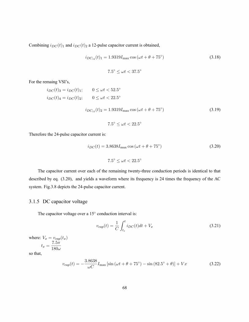
Combining iDC(t)1 and iDC(t)2 a 12-pulse capacitor current is obtained,
iDC12(t)1 = 1.9319Imax cos (ωt+ θ + 75) (3.18)
7.5 ≤ ωt < 37.5
For the remaing VSI’s,
iDC(t)3 = iDC(t)1; 0 ≤ ωt < 52.5
iDC(t)4 = iDC(t)2; 0 ≤ ωt < 22.5
iDC12(t)2 = 1.9319Imax cos (ωt+ θ + 75) (3.19)
7.5 ≤ ωt < 22.5
Therefore the 24-pulse capacitor current is:
iDC(t) = 3.8638Imax cos (ωt+ θ + 75) (3.20)
7.5 ≤ ωt < 22.5
The capacitor current over each of the remaining twenty-three conduction periods is identical to that
described by eq. (3.20), and yields a waveform where its frequency is 24 times the frequency of the AC
system. Fig.3.8 depicts the 24-pulse capacitor current.
3.1.5 DC capacitor voltage
The capacitor voltage over a 15 conduction interval is:
vcap(t) =1
C
Z t
tx
iDC(t)dt+ Vx (3.21)
where: Vx = vcap(tx)
tx =7.5π
180ωso that,
vcap(t) = −3.8638ωC
Imax [sin (ωt+ θ + 75)− sin (82.5 + θ)] + V x (3.22)
68

0 0.002 0.004 0.006 0.008 0.01 0.012 0.014 0.016-1.5
-1
-0.5
0
0.5
1
1.5
(a)
Am
p (p
u)
0 0.002 0.004 0.006 0.008 0.01 0.012 0.014 0.016-1.5
-1
-0.5
0
0.5
1
1.5
Time (s)
Am
p (p
u)
Fig. 3.8 Capacitor current; a)generating reactive power; b)absorbing reactive power
7.5 ≤ ωt < 22.5
To calculate the initial condition V0 at t = 0 s, first Vx will be calculated using the average component of eq.
(3.22).
VDC =1
T
tyZtx
vcap(t)dt (3.23)
where: T =π
12ω; ty =
22.5π
180ω
VDC = −46.3656πωC
Imax [cos (97.5 + θ)− cos (82.5 + θ)]− 3.8638
ωCImax sin (82.5
+ θ) + Vx (3.24)
Eq. (3.24) yields,
Vx = VDC +46.3656
πωCImax [cos (97.5
+ θ)− cos (82.5 + θ)] +3.8638
ωCImax sin (82.5
+ θ) (3.25)
if R = 0 then θ = 0,therefore,
Vx = VDC − 12.1039πωC
Imax +3.8307
ωCImax (3.26)
69

0 0.002 0.004 0.006 0.008 0.01 0.012 0.014 0.0160.985
0.99
0.995
1
1.005
1.01
(a)
Vol
ts (p
u)
0 0.002 0.004 0.006 0.008 0.01 0.012 0.014 0.0160.996
0.998
1
1.002
1.004
1.006
1.008
(b)Time (s)
Vol
ts (p
u)
Fig. 3.9 DC capacitor voltage; a)generating reactive power; b)absorbing reactive power
calculating V0; V0 = vcap(tz), where tz =15π
180ω
V0 =3.8638
ωCImax [sin (90
+ θ)− sin (82.5 + θ)] + Vx (3.27)
Fig.3.9 shows the 24-pulse DC-capacitor voltage.
3.2 48-pulse operation
Two 24-pulse converters, phase-shifted by 7.5 from each other, can provide a 48-pulse converter.
Using a symmetrical criterion the 7.5 are provided in the following way: phase-shift windings with -3.75
on the two transformers of one 24-pulse converter, and +3.75 on the two transformers of the other one. The
firing pulse needs a phase-shift of +3.75 and -3.75, respectively.
The 48-pulse converter is comprised by four 12-pulse converter linked by four 12-pulse transformers
with phase-shift windings (see Fig.3.4). Fig.3.10 depicts the schematic diagram of a 48-pulse STATCOM.
The transformer connexion and the necessary firing pulse logic to get the 48-pulse operation will be treated
in the next section.
70

3.2.1 48-pulse voltage
The 48-pulse converter can be used in high power applications without AC filters due to its high per-
formance and low harmonic rate on the AC side. The output voltage have harmonics n = 48r ± 1, where
r = 0, 1, 2, ...; i.e., 47th, 49th, 95th, 97th,..., with magnitudes of 1/47th, 1/49th , 1/95th, 1/97th, ..., respec-
tively, respect to the fundamental; on the DC side the lower circulating harmonic current will be the 48th.
The phase-shift pattern on each 12-pulse converter is the following:
1th 12-pulse converter
PST: +7.5 Necessary to eliminate the 24-pulse harmonics
+3.75 Necessary to eliminate the 48-pulse harmonics
Total +11.25 Winding turn rate 1:tan(11.25)
Driver: -7.5 Necessary to eliminate the 24-pulse harmonics
-3.75 Necessary to eliminate the 48-pulse harmonics
Total -11.25
The resultant output voltage generated by this 12-pulse converter is,
vab12(t)1 = 2[Vab1 sin (ωt+ 30) + Vab11 sin (11ωt+ 195
) + Vab13 sin (13ωt+ 255)
+Vab23 sin (23ωt+ 60) + Vab25 sin (25ωt+ 120
) + ...] (3.28)
2th 12-pulse converter
PST: -7.5 Necessary to eliminate the 24-pulse harmonics
+3.75 Necessary to eliminate the 48-pulse harmonics
Total -3.75 Winding turn rate 1:tan(3.75)
Driver: +7.5 Necessary to eliminate the 24-pulse harmonics
-3.75 Necessary to eliminate the 48-pulse harmonics
Total +3.75
The resultant output voltage generated by this 12-pulse converter is,
vab12(t)2 = 2[Vab1 sin (ωt+ 30) + Vab11 sin (11ωt+ 15
) + Vab13 sin (13ωt+ 75)
+Vab23 sin (23ωt+ 60) + Vab25 sin (25ωt+ 120
) + ...] (3.29)
3th 12-pulse converter
71

Fig. 3.10 48-pulse STATCOM
72

PST: +7.5 Necessary to eliminate the 24-pulse harmonics
-3.75 Necessary to eliminate the 48-pulse harmonics
Total +3.75 Winding turn rate 1:tan(3.75)
Driver: -7.5 Necessary to eliminate the 24-pulse harmonics
+3.75 Necessary to eliminate the 48-pulse harmonics
Total -3.75
The resultant output voltage generated by this 12-pulse converter is,
vab12(t)3 = 2[Vab1 sin (ωt+ 30) + Vab11 sin (11ωt+ 285
) + Vab13 sin (13ωt+ 345)
+Vab23 sin (23ωt+ 240) + Vab25 sin (25ωt+ 300
) + ...] (3.30)
4th 12-pulse converter
PST: -7.5 Necessary to eliminate the 24-pulse harmonics
-3.75 Necessary to eliminate the 48-pulse harmonics
Total -11.25 Winding turn rate 1:tan(11.25)
Driver: +7.5 Necessary to eliminate the 24-pulse harmonics
+3.75 Necessary to eliminate the 48-pulse harmonics
Total +11.25
The resultant output voltage generated by this 12-pulse converter is,
vab12(t)4 = 2[Vab1 sin (ωt+ 30) + Vab11 sin (11ωt+ 105
) + Vab13 sin (13ωt+ 165)
+Vab23 sin (23ωt+ 240) + Vab25 sin (25ωt+ 300
) + ...] (3.31)
These four 12-pulse AC output voltages, given by eqs. (3.29-3.31), are added connecting in series the
secondary windings of the transformers. The 48-pulse AC output voltage is given by:
vab48(t) = vab12(t)1 + vab12(t)2 + vab12(t)3 + vab12(t)4 (3.32)
vab48(t) = 8[Vab1 sin (ωt+ 30) + Vab47 sin (47ωt+ 150
) + Vab49 sin (49ωt+ 210)
+Vab95 sin (95ωt+ 330) + Vab97 sin (97ωt+ 30
) + ...] (3.33)
73

The general expression for the 12-pulse AC output voltage is given by:
vab12(t) = 2∞Xn=1
Vabn sin (nωt+ 30n) (3.34)
∀ n = 12r ± 1, r = 0, 1, 2, ...
Applying a 11.25 phase-shift provided by a PST to eq. (3.34),
vab12(t) = 2∞Xn=1
Vabn sin (nωt+ 30n+ 11.25i) (3.35)
∀ n = 12r ± 1, r = 0, 1, 2, ...
where: i = 1 for positive sequence harmonics, abc sequence.
i = -1 for negative sequence harmonics, cba sequence.
Now lagging the firing pulse 11.25, results,
vab12(t) = 2∞Xn=1
Vabn sin (nωt+ 18.75n+ 11.25i) (3.36)
∀ n = 12r ± 1, r = 0, 1, 2, ...
Therefore the general expression of the line-to-line voltage associated to a 48-pulse converter is given
by eq. (3.37),
vab48(t) = 8∞Xn=1
Vabn sin (nωt+ 18.75n+ 11.25i) (3.37)
∀ n = 48r ± 1, r = 0, 1, 2, ...
The line-to-neutral voltage is,
van48(t) =8√3[Vab1 sin (ωt)−Vab47 sin (47ωt)−Vab49 sin (49ωt)+Vab95 sin (95ωt)+Vab97 sin (97ωt)+ ...]
(3.38)
that can be expressed as,
van48(t) =8√3
∞Xn=1
Vabn sin (nωt+ 18.75n− 18.75i) (3.39)
74

0 0.005 0.01 0.015 0.02 0.025 0.03 0.035-10
-8
-6
-4
-2
0
2
4
6
8
10
Time (s)
Vol
ts (
×VD
C)
vab(t)van(t)
Fig. 3.11 48-pulse voltage
∀ n = 48r ± 1, r = 0, 1, 2, ...
Voltages vbn48(t) and vcn48(t) have a similar pattern except phase shifted by 120 and 240, respec-
tively, from van48(t). Fig.3.11 depicts the 48-pulse line-to-line and the line-to-neutral voltage; the harmonic
content is exhibited in Fig.3.12.
3.2.2 AC current signals
The low harmonic rate of a 48-pulse STATCOM allows to approach its AC current just by the funda-
mental signal, the typical AC current waveform is shown in Fig.3.13.
The AC current for the phase ’a’ is given by eq. (3.14), although for a 48-pulse converter Imax is given
by eq. (3.40),
Imax =Vm − 5.0927VDC
ωL(3.40)
The current will be leading when Vm < 5.0927VDC ; thus, the compensator is seen as a capacitor by
the AC system and the current flows from the compensator to the AC system; the current will be lagging
75

0 10 20 30 40 50 60 70 80 90 1000
0.01
0.02
0.03
0.04
0.05
0.06
0.07
0.08
0.09
0.1
nth. harmonic
Mag
nitu
de (p
er u
nit f
unda
men
tal)
Fig. 3.12 48-pulse voltage Fourier spectrum
when Vm > 5.0927VDC ; thus the compensator behaves as an inductor and the current flows from the AC
system to the compensator.
3.2.3 Capacitor current
The capacitor current is made up by the contribution of each one of the four 12-pulse VSI that com-
prising the 48-pulse STATCOM. The capacitor current will be calculated in similar way to that presented
for the 24-pulse. Summing the DC current of each 6-pulse VSI,
iDC(t) = iDC(t)1 + iDC(t)2 + iDC(t)3 + iDC(t)4 + iDC(t)5 + iDC(t)6 + iDC(t)7 + iDC(t)8 (3.41)
The current of each 6-pulse VSI is the following one,
iDC(t)1 = Imax cos (ωt+ θ + 60) ; 11.25 ≤ ωt < 71.25
iDC(t)2 = Imax cos (ωt+ θ + 90) ; 11.25 ≤ ωt < 41.25
iDC(t)3 = Imax cos (ωt+ θ + 60) ; 0 ≤ ωt < 56.25
iDC(t)4 = Imax cos (ωt+ θ + 90) ; 0 ≤ ωt < 26.25
iDC(t)5 = Imax cos (ωt+ θ + 60) ; 3.75 ≤ ωt < 63.75
76

iDC(t)6 = Imax cos (ωt+ θ + 90) ; 0 ≤ ωt < 33.75
iDC(t)7 = Imax cos (ωt+ θ + 60) ; 0 ≤ ωt < 48.75
iDC(t)8 = Imax cos (ωt+ θ + 90) ; 0 ≤ ωt < 18.75
The 48-pulse capacitor current shown in Fig.3.14 is given by the expression eq (3.42). Its frequency is
48 times the frequency of the AC system. The remaining 47 segments are expressed symilarly.
iDC(t) = 7.7276Imax cos (ωt+ θ + 75) (3.42)
11.25 ≤ ωt < 18.75
0 0.005 0.01 0.015 0.02 0.025 0.03 0.035 0.04 0.045 0.05-0.2
-0.15
-0.1
-0.05
0
0.05
0.1
0.15
0.2
Time (s)
Am
p
LeadingLagging
Fig. 3.13 AC current waveform, ia(t)
3.2.4 DC capacitor voltage
The capacitor voltage over a 7.5 conduction interval is given by eq. (3.43):
vcap(t) =7.7276
ωCImax [sin (ωt+ θ + 75)− sin (86.25 + θ)] + V x (3.43)
11.25 ≤ 5ωt < 18.7
77

0 0.002 0.004 0.006 0.008 0.01 0.012 0.014 0.016-1.5
-1
-0.5
0
0.5
1
1.5
(a)
Am
p (p
u)
0 0.002 0.004 0.006 0.008 0.01 0.012 0.014 0.016-1.5
-1
-0.5
0
0.5
1
1.5
(b)Time (s)
Am
p (p
u)
Fig. 3.14 Capacitor current; a)generating reactive power; b)absorbing reactive power
where: Vx = vcap(tx); tx =11.25π
180ω.
The initial condition V0 at t = 0 s given by the eq. (3.46) is calculated by the similar procedure used
previously,
VDC =1
T
Z ty
tx
vcap(t)dt (3.44)
where: T =π
24ω; tx =
11.25π
180ω; ty =
18.75π
180ω.
Vx = VDC +185.4624
πωCImax [cos (93.75
+ θ)− cos (86.25 + θ)] +7.7276
ωCImax sin (86.25
+ θ) (3.45)
V0 = vcap(tz); tz =15π
180ω
V0 =7.7276
ωCImax [sin (90
+ θ)− sin (86.25 + θ)] + Vx (3.46)
Fig.3.15 shows the capacitor voltage; the peak capacitor voltage occurs at ωt = 7.5 when the com-
pensator is generating reactive power.
78

0 0.002 0.004 0.006 0.008 0.01 0.012 0.014 0.016
0.994
0.996
0.998
1
1.002
1.004
(a)
Vol
ts (p
u)
0 0.002 0.004 0.006 0.008 0.01 0.012 0.014 0.0160.998
0.999
1
1.001
1.002
1.003
1.004
(b)Time (s)
Vol
ts (p
u)
Fig. 3.15 Capacitor voltage; a)generating reactive power; b)absorbing reactive power
3.3 Digital simulations
In this section digital simulations using the EMTDC/PSCAD are carried out in order to verify the
analytical expressions developed in previous sections. Two cases will be presented: (1) using a fixed DC
value, that is, considering a infinite capacitor, and (2) considering a finite capacitor.
The first one is shown in Fig.3.16 and Fig.3.17. (24- and 48-pulse respectively). In the second case
the capacitor ripple voltage effect is illustrated, Fig.3.18 and Fig.3.19 (24- and 48-pulse respectively). It is
worth noting that to get a good harmonic performance and small DC voltage ripple an appropriate size of
DC capacitor must be chosen. The parameters employed are:
C = 470 µF (24-pulse), 1000 µF (48-pulse).
L = 3mH
R = 0.2 Ω
Vm = 2.5 V
VDC = 1.5 V (24-pulse); 0.75 V (48-pulse).
Note that a resistor R is used as internal losses; thereby, a small phase-shift between the AC system
voltage and the STATCOM voltage should be used to supply the internal losses.
79

3.4 Conclusions
The simplest three-phase converter is the six-pulse converter however even at low rating a simple six-
pulse converter is unlikely in high power applications due to its harmonic distortion. To reduce the harmonic
distortion to an acceptable level the pulse order must be increased to 24- or 48-pulse.
To get the 24- and 48-pulse converter complex phase-shifting transformers are needed but an approx-
imate behaviour can be obtained using simple 12-pulse transformers; two 12-pulse transformers having
relative phase displacements of 15, quasi 24-pulse operation, and four 12-pulse transformers having 7.5,
quasi 48-pulse operation. The quasi 48-pulse operation allows a small circulation of 12- and 24- pulse order
harmonic due to the 12-pulse harmonics which are characteristic of each 12-pulse converter are not perfectly
cancelled, but the residual magnitude is acceptably small [4].
80
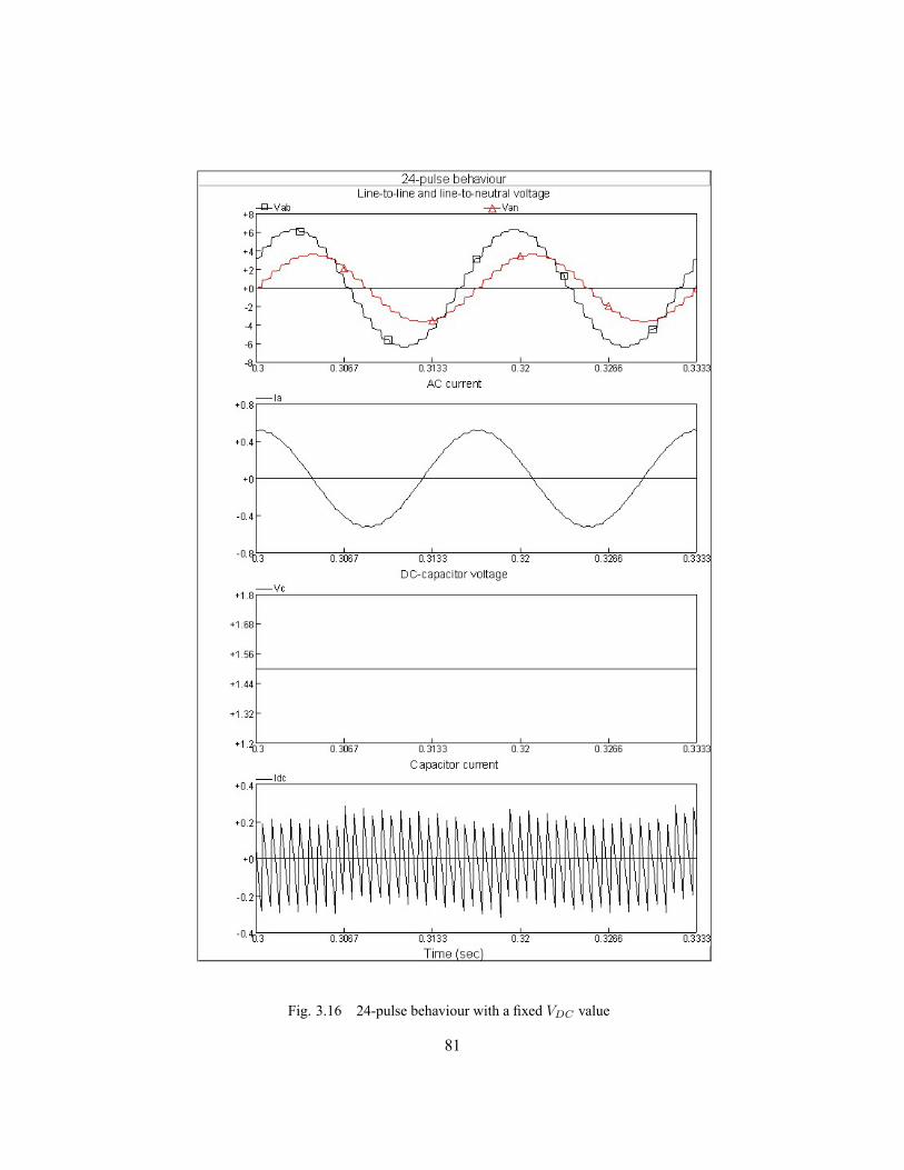
Fig. 3.16 24-pulse behaviour with a fixed VDC value
81

Fig. 3.17 24-pulse behaviour with a finite DC capacitor82

Fig. 3.18 48-pulse behaviour with fixed VDC value
83

Fig. 3.19 48-pulse behaviour with a finite DC capacitor
84

References[1] Naraing G. Hingorani, Laszlo Gyugyi, Understanding FACTS, IEEE Press 2000.
[2] M. R. Iravani, P. L. Dandeo, K. H. Nguyen, D. Zhu, d. Maratukulam, ”Applications of static phase
shifters in power systems,” IEEE Trans on Power Delivery, Vol 9, No. 3, July 1994, pp. 1600-1608.
[3] A. Krämer, J. Ruff, ”Transformers for phase angle regulation considering the selection of On-load
tap-changers,” IEEE Trans on Power Delivery, Vol. 13, No.2, April 1998, pp. 518-523.
[4] Yong Hua Song, Allan T. Johns, Flexible AC transmition systems FACTS, IEE Power and Energy
Series 30, 1999.
85

Chapter 4STATCOM Modelling
This chapter establishes a detailed procedure to model the STATCOM; a generalised model based on
switching functions [1] is developed. Based on such switching functions model, a state-space representation
in the dq-reference frame is deduced. The accuracy of the developed models are validated comparing the
analytical results and digital simulations using the EMTDC/PSCAD.
4.1 Switching functions model
The general model or switching functions model is based on the on/off transistor switching strategy,
the nonlinear characteristics of the transistors such as the turn off time and the turn on time and others are
neglected, the semiconductor devices are treated as ideal switches.
Fig.4.1 shows a three-phase bridge or six-pulse converter, this figure illustrates that each converter leg
is composed of a transistor (thyristor) and a diode to permit bi-directional current flow due to both devices
can be represented by a switch (neglecting losses). To describe the modelling procedures, the phase ‘a’
arm of the six-pulse converter is considered, where the semiconductor devices are represented by switches
Sw1 and Sw4; the resistance R in series with the inverter represents the sum of the transformer winding
resistance losses and the inverter conduction losses; the inductance L represents the leakage inductance of
the transformer, Fig.4.2.
The loop equation that described the behaviour of the STATCOM circuit can be expressed as
ean(t)− van(t) = L ddtia(t) +Ria(t) (4.1)
where van(t) is the converter output voltage determined by the gating signals and the DC voltage.
Regardless of the PWM technique the switches in one arm are complementary, that is, if the upper
switch is on the lower is off and vice-versa. fs1 is defined as the switching function of switch Sw1and fs4 of
Sw4. fs1 and fs4 are either 1 or 0 corresponding to on and off switch states respectively. Due to the switches
are complementary,
fs1 + fs4 = 1 (4.2)
86
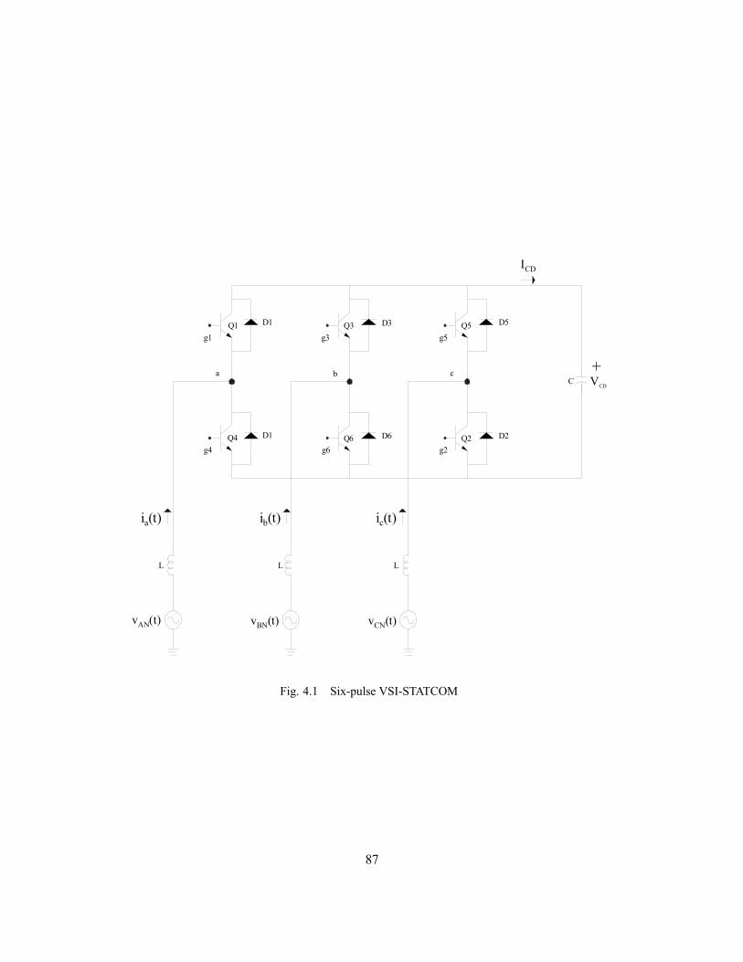
Q1
Q4
Q3 Q5
Q6 Q2
D1 D3 D5
D1 D6 D2
a b c
g1 g3 g5
g4 g6 g2
L L L
C
ICD
vAN(t) vBN(t) vCN(t)
VCD
+
ia(t) ib(t) ic(t)
Fig. 4.1 Six-pulse VSI-STATCOM
87

Q1
Q4
D1
D1
a
g1
g4
CLR
ean
iaVDC
iDC
Fig. 4.2 phase ’a’ arm
voltage van(t) is given by
van(t) = vFH(t) + vHn (4.3)
If Sw1 is on, fs1 = 1 and fs4 = 0, therefore,
vFH(t) = VDCfs1 (4.4)
on the other hand, if Sw4 is off, fs1 = 0 and fs4 = 1,then,
vFH(t) = 0 (4.5)
Therefore expressing eq. (4.3) as a function in terms of the switching function
van(t) = VDCfs1 + vHn(t) (4.6)
Substituting eq (4.6) into (4.1)
Ld
dtia(t) +Ria(t) = ean(t)− VDCfs1 − vHn(t) (4.7)
88

Similarly, for phases ‘b’ and ‘c’,
Ld
dtib(t) +Rib(t) = ebn(t)− VDCfs3 − vHn(t) (4.8)
Ld
dtic(t) +Ric(t) = ecn(t)− VDCfs5 − vHn(t) (4.9)
The vHn(t) voltage is measured from the negative VDC terminal to the neutral AC point. It is obtained
adding the equations of the three phases assuming a balanced system (ia + ib + ic = 0), so that
vHn(t) = −VDC3
Xi=1,3,5
fsi (4.10)
Substituting (4.10) into (4.7) the final expression for phase ‘a’ is deduced.
Ld
dtia(t) = −Ria(t)−
fs1 − 13 Xi=1,3,5
fsi
VDC + ean(t) (4.11)
similarly for phases ’b’ and ’c’,
Ld
dtib(t) = −Rib(t)−
fs3 − 13 Xi=1,3,5
fsi
VDC + ebn(t) (4.12)
Ld
dtic(t) = −Ric(t)−
fs5 − 13 Xi=1,3,5
fsi
VDC + ecn(t) (4.13)
The above equations show three of the four equations, three currents and the capacitor voltage-the DC
voltage-. Deducing the expression for the DC capacitor voltage, we have
iDC(t) = Cd
dtvDC(t) (4.14)
From chapter 2 we know that
iDC(t) = ia(t)fs1 + ib(t)fs3 + ic(t)fs5 (4.15)
iDC(t) =Xi=1,3,5
Xj=a,b,c
ij(t)fsi (4.16)
therefored
dtvDC(t) =
1
C(ia(t)fs1 + ib(t)fs3 + ic(t)fs5) (4.17)
89

The generalised model or switching function model for a six-pulse converter is given by equations
(4.11)-(4.17), where the adopted pulse-width modulation (PWM) scheme is taking into account on the
switching functions fsi .
The multi-pulse converters 12-, 24- and 48-pulse are comprised by the union of 6-pulse converters, the
lowest practical and building block of multi-pulse converters is the 12-pulse converter; it is comprised by
two 6-pulse converters linked by a 12-pulse transformer (see chapter 2) with a common DC capacitor. In the
next section the model developed above will be extended to a 12-pulse converter, the interaction between
the two six-pulse converter will be studied.
4.1.1 12-pulse converter
For a 12-pulse converter the contribution of the second six-pulse converter linked by the ∆-Y trans-
former must be taken into account. The line-to-neutral voltage van(t) due to a 12-pulse converter is given
by eq. (4.18).
van(t) = van(t)Y Y + van(t)∆Y (4.18)
where van(t)Y Y is the line-to-neutral voltage in the secondary winding of the Y-Y transformer, and van(t)∆Yis the line-to-neutral voltage in the secondary winding of the ∆-Y transformer. van(t)Y Y was calculated
above, eq. (4.6).
The line-to-neutral voltage in the secondary winding of the ∆-Y transformer is calculated using the
line-to-line voltage of the three phase bridge. The line-to-line voltage of the six-pulse converter linked by
the Y-Y transformer vab(t)Y is given by
vab(t)Y = van(t)Y Y − vbn(t)Y Y (4.19)
where: van(t)Y Y = vDC(t)fs1 + vHn(t)
vbn(t)Y Y = vDC(t)fs3 + vHn(t)
so that
vab(t)Y = vDC(t) (fs1 + fs3) (4.20)
in the∆-Y six-pulse converter the line-to-line voltage on the delta side is
vab(t)∆ = vDC(t) (fs12 + fs32) (4.21)
90
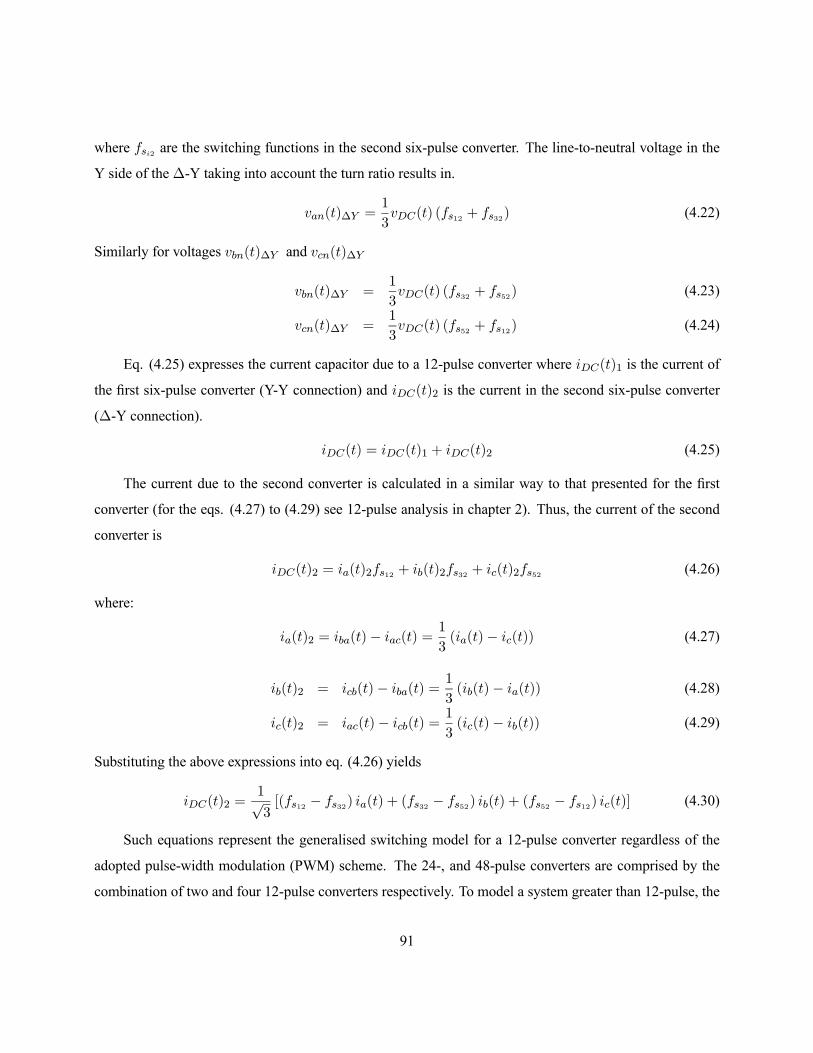
where fsi2 are the switching functions in the second six-pulse converter. The line-to-neutral voltage in the
Y side of the∆-Y taking into account the turn ratio results in.
van(t)∆Y =1
3vDC(t) (fs12 + fs32) (4.22)
Similarly for voltages vbn(t)∆Y and vcn(t)∆Y
vbn(t)∆Y =1
3vDC(t) (fs32 + fs52) (4.23)
vcn(t)∆Y =1
3vDC(t) (fs52 + fs12) (4.24)
Eq. (4.25) expresses the current capacitor due to a 12-pulse converter where iDC(t)1 is the current of
the first six-pulse converter (Y-Y connection) and iDC(t)2 is the current in the second six-pulse converter
(∆-Y connection).
iDC(t) = iDC(t)1 + iDC(t)2 (4.25)
The current due to the second converter is calculated in a similar way to that presented for the first
converter (for the eqs. (4.27) to (4.29) see 12-pulse analysis in chapter 2). Thus, the current of the second
converter is
iDC(t)2 = ia(t)2fs12 + ib(t)2fs32 + ic(t)2fs52 (4.26)
where:
ia(t)2 = iba(t)− iac(t) = 1
3(ia(t)− ic(t)) (4.27)
ib(t)2 = icb(t)− iba(t) = 1
3(ib(t)− ia(t)) (4.28)
ic(t)2 = iac(t)− icb(t) = 1
3(ic(t)− ib(t)) (4.29)
Substituting the above expressions into eq. (4.26) yields
iDC(t)2 =1√3[(fs12 − fs32) ia(t) + (fs32 − fs52) ib(t) + (fs52 − fs12) ic(t)] (4.30)
Such equations represent the generalised switching model for a 12-pulse converter regardless of the
adopted pulse-width modulation (PWM) scheme. The 24-, and 48-pulse converters are comprised by the
combination of two and four 12-pulse converters respectively. To model a system greater than 12-pulse, the
91

contribution of each 12-pulse unit must be taken into account with the appropriate phase shift in the gating
signals.
From Fig.4.3 to Fig.4.6 the behaviour of the 6-, 12-, 24-, and 48-pulse converter obtained with the
developed model is shown. The parameters used are as follows.
• Six-pulseVm = 2.5 V, VDC = 6 V, R = 0.2 Ω, L = 3mH, C = 1000 µF, α = −6o
• 12-pulseVm = 2.5 V, VDC = 3 V, R = 0.4 Ω, L = 6mH, C = 1000 µF, α = −5.5o
• 24-pulseVm = 2.5 V, VDC = 1.5 V, R = 0.8 Ω, L = 12mH, C = 1000 µF, α = −6o
• 48-pulseVm = 2.5 V, VDC = 0.75 V, R = 1.6 Ω, L = 24mH, C = 1000 µF, α = −5.85o
The results obtained in this section are comparable with the ones shown in previous sections.
4.2 STATCOM model at fundamental frequency
The main advantage of the switching model is that it is applicable to various forms of pulse-width
modulation (PWM) or to other switching strategies [1], although it is a model that is hard to work applying
classical control theory, there are a few methods and tools in the theory of nonlinear dynamics that have
proved be very useful in studying the behaviour of power electronic converters; sliding mode schemes have
also been proposed on the basis of switching models [2-4].
Due to the complexity of the switching models, the modelling is typically performed using an approx-
imate continuous time representation (average models) of the converter in the synchronous reference frame
(dq). The conventional averaging technique gives a useful representation of the system and allows simple
design procedures for operation in certain regimes; however, there are several limitations to this modelling
approach. These include the inability to [5]:
• Represent the inherent discrete time nature of the VSI switching, which limits the closed loop perfor-mance of the VSI.
• Account for the effect harmonics on the steady-state fundamental frequecy behaviour of the VSI.
• Model resonances, occurring between the AC and DC sides of the VSI, as well as those between the AC
92

0.3 0.305 0.31 0.315 0.32 0.325 0.33 0.335 0.34 0.345 0.35-2
-1
0
1
2AC current ia(t)
Am
p
0.3 0.305 0.31 0.315 0.32 0.325 0.33 0.335 0.34 0.345 0.35-10
-5
0
5
10Line-to-line and Line-to-neutral voltage
Vol
ts
vab(t)van(t)
0.3 0.305 0.31 0.315 0.32 0.325 0.33 0.335 0.34 0.345 0.35-1
-0.5
0
0.5
1Capacitor current
Am
p
0.3 0.305 0.31 0.315 0.32 0.325 0.33 0.335 0.34 0.345 0.355.6
5.8
6
6.2
6.4
Capacitor voltage
Time (s)
Vol
ts
Fig. 4.3 Six-pulse behaviour
93

0.3 0.305 0.31 0.315 0.32 0.325 0.33 0.335 0.34 0.345 0.35-1
-0.5
0
0.5
1AC current ia(t)
Am
p
0.3 0.305 0.31 0.315 0.32 0.325 0.33 0.335 0.34 0.345 0.35-10
-5
0
5
10Line-to-line and Line-to-neutral voltage
Vol
ts
vab(t)van(t)
0.3 0.305 0.31 0.315 0.32 0.325 0.33 0.335 0.34 0.345 0.35-0.4
-0.2
0
0.2
0.4Capacitor current
Am
p
0.3 0.305 0.31 0.315 0.32 0.325 0.33 0.335 0.34 0.345 0.35
2.95
3
3.05
Capacitor voltage
Time (s)
Vol
ts
Fig. 4.4 12-pulse behaviour
94

0.3 0.305 0.31 0.315 0.32 0.325 0.33 0.335 0.34 0.345 0.35-0.4
-0.2
0
0.2
0.4AC current ia(t)
Am
p
0.3 0.305 0.31 0.315 0.32 0.325 0.33 0.335 0.34 0.345 0.35-10
-5
0
5
10Line-to-line and Line-to-neutral voltage
Vol
ts
vab(t)van(t)
0.3 0.302 0.304 0.306 0.308 0.31 0.312 0.314 0.316-0.2
-0.1
0
0.1
0.2Capacitor current
Am
p
0.3 0.302 0.304 0.306 0.308 0.31 0.312 0.314 0.316 0.318 0.32
1.46
1.48
1.5
1.52
1.54
1.56Capacitor voltage
Time (s)
Vol
ts
Fig. 4.5 24-pulse behaviour
95

0.3 0.305 0.31 0.315 0.32 0.325 0.33 0.335 0.34 0.345 0.35-0.2
-0.1
0
0.1
0.2AC current ia(t)
Am
p
0.3 0.305 0.31 0.315 0.32 0.325 0.33 0.335 0.34 0.345 0.35-10
-5
0
5
10Line-to-line and Line-to-neutral voltage
Vol
ts
vab(t)van(t)
0.3 0.302 0.304 0.306 0.308 0.31 0.312 0.314 0.316-0.1
-0.05
0
0.05
0.1Capacitor current
Am
p
0.3 0.302 0.304 0.306 0.308 0.31 0.312 0.314 0.316
0.745
0.75
0.755
Capacitor voltage
Time (s)
Vol
ts
Fig. 4.6 48-pulse behaviour
96

system and the VSI controls.
• Calculate AC and DC side harmonic injections generated by the converter switching.
Models based on time averaging theory have been proposed [6, 7]. This section presents the continuous
STATCOM time model at fundamental frequency. The output voltages (line-to-line and line-to-neutral) and
the phase currents are approximated just by their fundamental components; for high pulse-numbered (24-
and 48-pulse) converters it is a good approximation. The capacitor current and voltage are approximated by
its average components.
To develop the model the only assumption is that the switching pattern is symmetrical. The functions
f0si are the average functions (fundamental frequency) of the switching functions defined previously. The
function fs1 expressed by its Fourier series is given by eq (4.31),
fs1 = a0 +∞Xn=1
(an cos (nωt) + bn sin (nωt)) (4.31)
where
a0 =1
2; an = 0,
bn =2
nπ∀ n odd
so that the fundamental component of fs1 is
f0s1 =1
2+2
πsin (ωt) (4.32)
The expressions for f0s3 and f0s5 are similar to eq. (4.32) just phase-shift by -120oand -240o, respectively,
that is,
f0s3 =1
2+2
πsin (ωt− 120o) (4.33)
f0s5 =1
2+2
πsin (ωt− 240o) (4.34)
substituting eqs. (4.32), (4.33), and (4.34) into eq. (4.6) and (4.10) the voltages van(t) and vHn(t) at
fundamental frequency, v0an(t), v0Hn(t) are obtained given by eqs. (4.35) and (4.36).
v0Hn(t) = −1
2vDC(t) (4.35)
v0an(t) =2
πvDC(t) sin (ωt) (4.36)
97
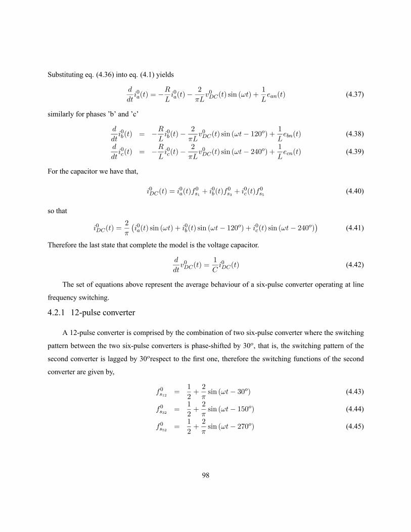
Substituting eq. (4.36) into eq. (4.1) yields
d
dti0a(t) = −
R
Li0a(t)−
2
πLv0DC(t) sin (ωt) +
1
Lean(t) (4.37)
similarly for phases ’b’ and ’c’
d
dti0b(t) = −R
Li0b(t)−
2
πLv0DC(t) sin (ωt− 120o) +
1
Lebn(t) (4.38)
d
dti0c(t) = −R
Li0c(t)−
2
πLv0DC(t) sin (ωt− 240o) +
1
Lecn(t) (4.39)
For the capacitor we have that,
i0DC(t) = i0a(t)f
0s1 + i
0b(t)f
0s3 + i
0c(t)f
0s5 (4.40)
so that
i0DC(t) =2
π
¡i0a(t) sin (ωt) + i
0b(t) sin (ωt− 120o) + i0c(t) sin (ωt− 240o)
¢(4.41)
Therefore the last state that complete the model is the voltage capacitor.
d
dtv0DC(t) =
1
Ci0DC(t) (4.42)
The set of equations above represent the average behaviour of a six-pulse converter operating at line
frequency switching.
4.2.1 12-pulse converter
A 12-pulse converter is comprised by the combination of two six-pulse converter where the switching
pattern between the two six-pulse converters is phase-shifted by 30o, that is, the switching pattern of the
second converter is lagged by 30orespect to the first one, therefore the switching functions of the second
converter are given by,
f0s12 =1
2+2
πsin (ωt− 30o) (4.43)
f0s32 =1
2+2
πsin (ωt− 150o) (4.44)
f0s52 =1
2+2
πsin (ωt− 270o) (4.45)
98

The fundamental component of the voltage in the secondary winding (Y side) of the∆− Y transformer is
v0an(t)∆Y =2
πv0DC(t) sin (ωt)
therefore the output voltages of a 12-pulse converter at fundamental frequency are
v0an(t)12 =4
πv0DC(t) sin (ωt) (4.46)
v0bn(t)12 =4
πv0DC(t) sin (ωt− 120o) (4.47)
v0cn(t)12 =4
πv0DC(t) sin (ωt− 240o) (4.48)
To calculate the contribution of the second converter in the capacitor current, the fundamental switching
functions are substituted into eq. (4.30), yielding,
i0DC(t)2 =1√3
¡¡f0s12 − f0s32
¢i0a(t) +
¡f0s32 − f0s52
¢i0b(t) +
¡f0s52 − f0s12
¢i0c(t)
¢(4.49)
so that,
i0DC(t)2 =2
π
¡i0a(t) sin (ωt) + i
0b(t) sin (ωt− 120o) + i0c(t) sin (ωt− 240o)
¢(4.50)
Therefore the average capacitor current due to a 12-pulse converter is given by eq. (4.51)
i0DC(t) =4
π
¡i0a(t) sin (ωt) + i
0b(t) sin (ωt− 120o) + i0c(t) sin (ωt− 240o)
¢(4.51)
4.2.2 24-pulse converter
The 24-pulse converter is comprised by two 12-pulse converters with a phase-shift of 15obetween them
(one of them lagged 7.5oand the other leaded 7.5o). From chapter 3 we know that the 24-pulses line-to-
neutral voltage is given by
v0an(t)24 =4√3Vab1 sin (ωt) (4.52)
where
Vab1 =2√3
πv0DC(t),
therefore the 24-pulse line-to-neutral voltages at fundamental frequency are given by the following expres-
99

sions:
v0an(t)24 =8
πv0DC(t) sin (ωt) (4.53)
v0bn(t)24 =8
πv0DC(t) sin (ωt− 120o) (4.54)
v0cn(t)24 =8
πv0DC(t) sin (ωt− 240o) (4.55)
To obtain the capacitor current we have to take into account the contribution of each 12-pulse converter.
When the firing angle of one 12-pulse converter is zero the capacitor current is given by eq. (4.51); in the
24-pulse converter one 12-pulse converter is lagged 7.5oand the other one leaded 7.5o, the DC current of
each 12-pulse converter is given by the expressions (4.56) for the lagging case and (4.57) for the leading
case.
i0DC12(t)1 =4
π
¡i0a(t) sin (ωt− 7.5o) + i0b(t) sin (ωt− 127.5o) + i0c(t) sin (ωt− 247.5o)
¢(4.56)
i0DC12(t)2 =4
π
¡i0a(t) sin (ωt+ 7.5
o) + i0b(t) sin (ωt− 112.5o) + i0c(t) sin (ωt− 232.5o)¢
(4.57)
Thus, the capacitor current in the 24-pulse converter is
i0DC(t)24 = i0DC12(t)1 + i
0DC12(t)2
so that,
i0DC(t)24 =8
π
¡i0a(t) sin (ωt) + i
0b(t) sin (ωt− 120o) + i0c(t) sin (ωt− 240o)
¢(4.58)
4.2.3 48-pulse converter
A similar procedure to the above presented is carried out to obtain the signals of a 48-pulse converter.
For a 48-pulse converter we have that,
v0an(t)48 = 2v0an(t)24 (4.59)
i0DC(t)48 = 2i0DC(t)24 (4.60)
According to the results obtained previously and including, the output voltage angle α or firing angle
as a control variable, that is, the switching pattern applied to transistors, the STATCOM state-space model
100

at fundamental frequency is given by,
·x (t) = Asx(t) +Bsu(t) (4.61)
where
x(t) =£i0a(t), i
0b(t), i
0c(t), v
0DC(t)
¤Tu(t) = [ean(t), ebn(t), ecn(t)]
T
As =
−RL
0 0 −k1 sin (ωt+ α)
0 −RL
0 −k1 sin (ωt+ α− 120o)0 0 −R
L−k1 sin (ωt+ α− 240o)
k2 sin (ωt+ α) k2 sin (ωt+ α− 120o) k2 sin (ωt+ α− 240o) 0
Bs =
1
L0 0
01
L0
0 01
L
k1 =2
πL; k2 =
2
πCFor a six-pulse converter
k1 =4
πL; k2 =
4
πCFor a 12-pulse converter
k1 =8
πL; k2 =
8
πCFor a 24-pulse converter
k1 =16
πL; k2 =
16
πCFor a 48-pulse converter
The model given by eq. (4.61) although appears to be linear, it is nonlinear. The nonlinearity of the
STATCOM is manifested by the inclusion of the control angle α on the state equation. Changes in the
control angle α will results in nonlinear responses in the STATCOM states [8].
4.3 dq0 Reference frame model
The Park’s transformation is used to develop the time-invariant form of eq. (4.61) in the rotating
reference frames (dq0). The Park’s transformation expressions used are given by the follows relationships
[9].
Xdq0 = TXabc (4.62)
101

Xabc = T−1Xdq0 (4.63)
T =
cos (ωt) cos (ωt− 120o) cos (ωt− 240o)− sin (ωt) − sin (ωt− 120o) − sin (ωt− 240o)
1
2
1
2
1
2
(4.64)
The application of the Park’s transformation to an ’abc’ system eq. (4.65) yields to its equivalent in the
dq0 reference frame eq. (4.66).·x (t)abc = Ax(t)abc +Bu(t)abc (4.65)
·xdq0= TAT
−1xdq0 + TBT−1udq0 + ωxqd0 (4.66)
Applying the Park’s transformation to the fundamental frequency model eq. (4.61) of the STATCOM
yields " ·idq0·vDC
#=
·T 00 1
¸" ·iabc·vDC
#+ ω
·iqd00
¸(4.67)
where: iqd0 = [iq,−id, 0]T , so that" ·idq0·vDC
#=
·TAs11T
−1 TAs12As21T
−1 As22
¸ ·idq0vDC
¸+
·TBsT
−1 00 0
¸ ·edq00
¸+ ω
·iqd00
¸(4.68)
where:
TAs11T−1 = diagonal
½−RL
¾; TAs12 = [−k1 sin(α), k1 cos (α) , 0]T ;
As21T−1 =
·3
2k2 sin (α) ,−3
2k2 cos (α) , 0
¸As22 = [0] ; TBsT
−1 = diagonal½1
L
¾Finally the STATCOM model in the dq0 reference frame can be represented by
·xdq0= Adq0xdq0 +Bdq0udq0 (4.69)
where:
xdq0 = [id, iq, i0, vDC ]T
udq0 = [ed, eq, e0, 0]T
102

Adq0 =
−RL
ω 0 −k1 sin (α)−ω −R
L0 k1 cos (α)
0 0 −RL
0
3
2k2 sin (α) −3
2k2 cos (α) 0 0
Bdq0 =
1
L0 0 0
01
L0 0
0 01
L0
0 0 01
C
Expressing in other form
d
dtid = −R
Lid − k1 sin (α) vDC + 1
Led + ωiq
d
dtiq = −R
Liq + k1 cos (α) vDC +
1
Leq − ωid (4.70)
d
dtvDC =
3
2k2 [id sin (α)− iq cos (α)]
The states of the model are the dq0 components of the phase current and the voltage capacitor; the
inputs are the dq0 components of AC voltage where the STATCOM is connected.
Figures Fig.4.7-Fig.4.9 show the response of each model, the fundamental frequency model and the dq0
model. Figures depict the response of a 48-pulse STATCOM using the parameters previously mentioned.
The converter is initially at steady state with α = −6o, at time t = 0.3 s the angle α was stepped from -6oto
-9o. It should be noted that the model at fundamental frequency and the dq0 model do not take into account
the switching effects; this can be seen in the capacitor voltage, Fig.4.9.
4.4 Conclusions
Independent of the application, modelling for power system analysis is typically performed using an
approximate continuous time representation of the converter in the synchronous reference frame (dq0).
The continuous time model of the VSI yields a set of three differential equations which represent the VSI
operation with reasonable accuracy under most conditions, but these models present some limitations such
103
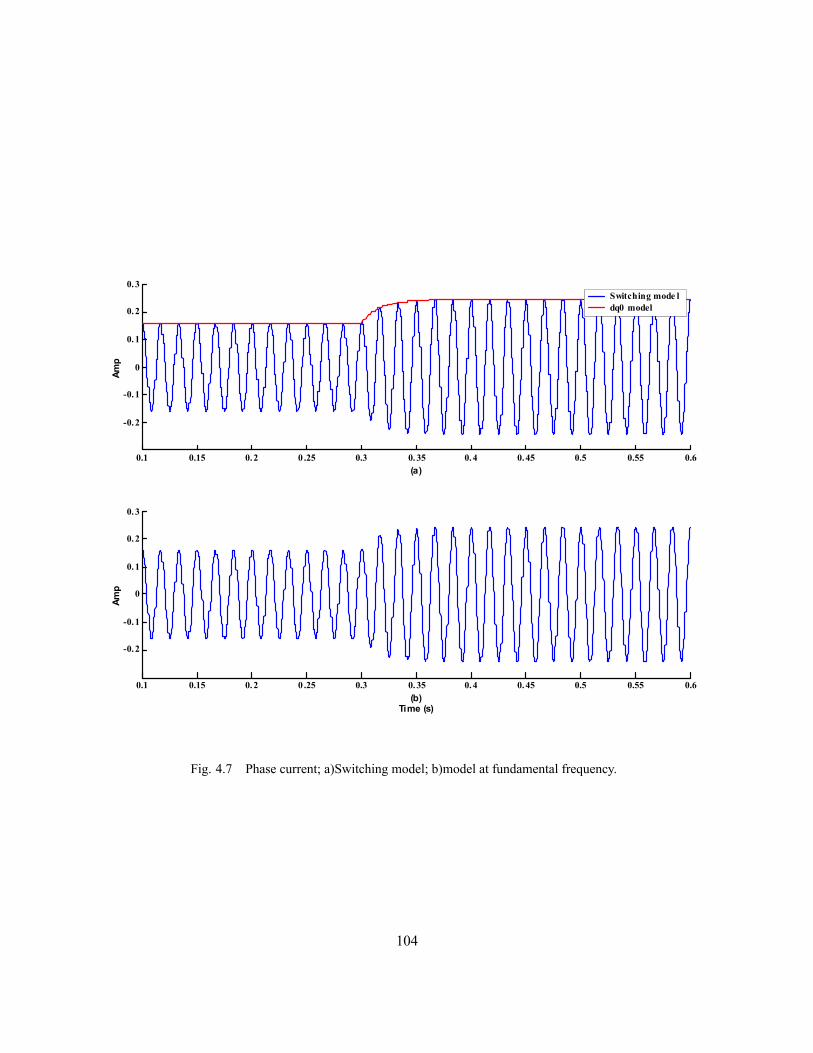
0.1 0.15 0.2 0 .25 0.3 0. 35 0.4 0.45 0.5 0.55 0.6
-0.2
-0.1
0
0.1
0.2
0.3
(a)
Amp
Switching mode ldq0 model
0.1 0.15 0.2 0 .25 0.3 0. 35 0.4 0.45 0.5 0.55 0.6
-0.2
-0.1
0
0.1
0.2
0.3
(b)Time (s)
Amp
Fig. 4.7 Phase current; a)Switching model; b)model at fundamental frequency.
104

0.1 0.15 0.2 0.25 0.3 0.35 0.4 0.45 0.5 0.55 0.60.15
0.2
0.25id component
0.1 0.15 0.2 0.25 0.3 0.35 0.4 0.45 0.5 0.55 0.6-0.04
-0.035
-0.03
-0.025
-0.02
-0.015
Time (s)
iq component
Fig. 4.8 id and iq current
105
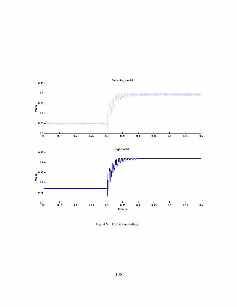
0.1 0.15 0.2 0.25 0.3 0.35 0.4 0.45 0.5 0.55 0.60.7
0.75
0.8
0.85
0.9
0.95
Time (s)
Vol
ts
dq0 model
0.1 0.15 0.2 0.25 0.3 0.35 0.4 0.45 0.5 0.55 0.60.7
0.75
0.8
0.85
0.9
0.95
Vol
ts
Switching model
Fig. 4.9 Capacitor voltage
106

as the inability to represent the switching effects.
Switching models describe very well the dynamic of the VSI taking into account the switching effects
but these kinds of models are very complicated and hard to work with linear theory, although there are a
few methods and tools in the theory of nonlinear dynamics that have proved very useful in studying the
behaviour of power electronic converters.
107

References[1] Seyed Ali Nabavi-Niaki, ”Modelling and applications of unified power flow controller (UPFC) for
power systems”, Ph. D. Thesis, University of Toronto, 1996.
[2] Banerjee, Verghese, ”Nonlinear Phenomena in power electronics”, IEEE Press, 2001.
[3] J. Kassakian, M. Schlecht, and G. Verghese, ”Principles of power electronics”, Addison-Wesley,
1991.
[4] IEEE, ”Special Issue on hybrid systems”, IEEE Trans. on Automatic Control, May 1998
[5] P. W. Lehn, ”Exact modeling of the Voltage Source Converter”, IEEE Trans. on Power Delivery, Vol.
17, No. 1, pp. 217-222, January 2002
[6] P. W. Lehn, M. R. Iravani, ”Experimental Evaluation of STATCOM Closed Loop”, IEEE Trans. on
Power Delivery, Vol. 13, No. 4, pp. 1378-1384, October 1998.
[7] K. R. Padiyar, A. M. Kulkarni, ”Design of reactive current and voltage controller of static condenser”,
Electrical Power and Energy Systems, Vol.19, No. 6, pp. 397-410, 1997.
[8] Pranesh Rao, M. L. Crow, Zhiping Yang, ”STATCOM Control for power system voltage control
applications”, IEEE Trans. on Power Delivery, Vol 15, No. 4, pp. 1311-1317, October 2000.
[9] P. Kundur, ”Power System Stability and Control”, McGraw Hill, 1994.
108

ConclusionsThe STATCOM and other FACTS devices have been widely studied by analytical models but the physi-
cal functionality is unknown for a lot of power researches. Understand the physical functionality and present
clearly the design and development of a real three-phase STATCOM prototype laboratory is the biggest mo-
tivation of this work.
Chapter 2 explains the relevant details of the voltage source-inverter (VSI), the building block of a
STATCOM and other FACTS devices. A detailed analysis is carried out to deduce the expressions for
the AC (phase currents and output voltage) and DC signals (capacitor current and voltage) of a 6- and
12-pulse STATCOM. The resulting expressions allow to approximate an adequate DC capacitor value. A
VSI generates an AC voltage from a DC voltage, when a VSI is used as a typical STATCOM a fixed
DC capacitor is used as a DC source. An important questions about that are answered: how the energy
conversion is achieved using a DC capacitor?, and if a DC source is not used, how the capacitor voltage
is kept fixed?. Such questions are answered establishing that, when the compensator (neglecting losses) is
exchanging reactive power only, the average power across the DC capacitor is zero, therefore the capacitor
does not change its voltage.
The control mechanism to regulate the capacitor voltage and therefore, the control of the active and
reactive power is demonstrated using the active power exchange to decrease/increase the capacitor voltage,
controlling the switching angle pattern of the semiconductor devices.
The simplest three-phase converter is the six-pulse converter however even at low rating a simple six-
pulse converter is unlikely in high power applications due to its harmonic distortion. To reduce the harmonic
distortion to an acceptable level the pulse order must be increased to 24- or 48-pulse. To get the 24- and
48-pulse converter complex phase-shifting transformers are needed but an approximate behaviour can be
obtained using simple 12-pulse transformers; two 12-pulse transformers having relative phase displacements
of 15, quasi 24-pulse operation, and four 12-pulse transformers having 7.5, quasi 48-pulse operation. The
quasi 48-pulse operation allows a small circulation of 12- and 24- pulse order harmonic due to the 12-pulse
harmonics which are characteristic of each 12-pulse converter are not perfectly cancelled, but the residual
magnitude is acceptably small.
In power system analysis, modelling is typically performed using an approximate continuous time rep-
resentation of the converter in the synchronous reference frame (dq0). The continuous time model of the VSI
109

yields a set of three differential equations which represent the VSI operation with reasonable accuracy under
most conditions, but these models present some limitations such as the inability to represent the switching
effects. Switching models describe very well the dynamic of the VSI taking into account the switching ef-
fects but these kinds of models are very complicated and hard to work with linear theory, although there are
a few methods and tools in the theory of nonlinear dynamics that have proved very useful in studying the
behaviour of power electronic converters.
110

Future workUsing this theoretical analysis an IGBT-12-pulse-VSI STATCOM will be developed first in digital sim-
ulations using the EMTDC/PSCAD software and then as a laboratory prototype. The prototype is comprised
by the power part (IGBT-12-pulse-VSI) and the control part (internal control and external control).
The internal control is an integral part of the converter. Its main function is to operate the converter
power switches so as to generate a fundamental output voltage waveform with the needed magnitude and
phase angle in synchronism with the AC system that forces the reactive power exchange required for com-
pensation.
The internal control is comprised by the IGBT-gate driver and by a microcontroller device that compute
the magnitude and phase angle of the required output voltage from the reactive and/or real power reference
signals, generating a set of coordinated gating pattern which determines the ”on” and ”off” periods of each
power devices. The reference signals are provided by the external control. The external control is determined
by the functional operation of the STATCOM, that is, the final application: power flow control, loop-flow
control, voltage regulation, enhancement of transient stability or damping of power oscillations.
111